JP7444875B2 - Voltage waveform generator for plasma processing equipment - Google Patents
Voltage waveform generator for plasma processing equipment Download PDFInfo
- Publication number
- JP7444875B2 JP7444875B2 JP2021524442A JP2021524442A JP7444875B2 JP 7444875 B2 JP7444875 B2 JP 7444875B2 JP 2021524442 A JP2021524442 A JP 2021524442A JP 2021524442 A JP2021524442 A JP 2021524442A JP 7444875 B2 JP7444875 B2 JP 7444875B2
- Authority
- JP
- Japan
- Prior art keywords
- plasma processing
- processing apparatus
- output
- voltage waveform
- waveform generator
- Prior art date
- Legal status (The legal status is an assumption and is not a legal conclusion. Google has not performed a legal analysis and makes no representation as to the accuracy of the status listed.)
- Active
Links
Images


Classifications
-
- H—ELECTRICITY
- H01—ELECTRIC ELEMENTS
- H01J—ELECTRIC DISCHARGE TUBES OR DISCHARGE LAMPS
- H01J37/00—Discharge tubes with provision for introducing objects or material to be exposed to the discharge, e.g. for the purpose of examination or processing thereof
- H01J37/32—Gas-filled discharge tubes
- H01J37/32009—Arrangements for generation of plasma specially adapted for examination or treatment of objects, e.g. plasma sources
- H01J37/32082—Radio frequency generated discharge
- H01J37/32137—Radio frequency generated discharge controlling of the discharge by modulation of energy
- H01J37/32146—Amplitude modulation, includes pulsing
-
- H—ELECTRICITY
- H05—ELECTRIC TECHNIQUES NOT OTHERWISE PROVIDED FOR
- H05H—PLASMA TECHNIQUE; PRODUCTION OF ACCELERATED ELECTRICALLY-CHARGED PARTICLES OR OF NEUTRONS; PRODUCTION OR ACCELERATION OF NEUTRAL MOLECULAR OR ATOMIC BEAMS
- H05H1/00—Generating plasma; Handling plasma
- H05H1/24—Generating plasma
- H05H1/46—Generating plasma using applied electromagnetic fields, e.g. high frequency or microwave energy
- H05H1/4645—Radiofrequency discharges
- H05H1/4652—Radiofrequency discharges using inductive coupling means, e.g. coils
-
- C—CHEMISTRY; METALLURGY
- C23—COATING METALLIC MATERIAL; COATING MATERIAL WITH METALLIC MATERIAL; CHEMICAL SURFACE TREATMENT; DIFFUSION TREATMENT OF METALLIC MATERIAL; COATING BY VACUUM EVAPORATION, BY SPUTTERING, BY ION IMPLANTATION OR BY CHEMICAL VAPOUR DEPOSITION, IN GENERAL; INHIBITING CORROSION OF METALLIC MATERIAL OR INCRUSTATION IN GENERAL
- C23C—COATING METALLIC MATERIAL; COATING MATERIAL WITH METALLIC MATERIAL; SURFACE TREATMENT OF METALLIC MATERIAL BY DIFFUSION INTO THE SURFACE, BY CHEMICAL CONVERSION OR SUBSTITUTION; COATING BY VACUUM EVAPORATION, BY SPUTTERING, BY ION IMPLANTATION OR BY CHEMICAL VAPOUR DEPOSITION, IN GENERAL
- C23C14/00—Coating by vacuum evaporation, by sputtering or by ion implantation of the coating forming material
- C23C14/22—Coating by vacuum evaporation, by sputtering or by ion implantation of the coating forming material characterised by the process of coating
- C23C14/34—Sputtering
- C23C14/3435—Applying energy to the substrate during sputtering
- C23C14/345—Applying energy to the substrate during sputtering using substrate bias
-
- H—ELECTRICITY
- H01—ELECTRIC ELEMENTS
- H01J—ELECTRIC DISCHARGE TUBES OR DISCHARGE LAMPS
- H01J37/00—Discharge tubes with provision for introducing objects or material to be exposed to the discharge, e.g. for the purpose of examination or processing thereof
- H01J37/32—Gas-filled discharge tubes
- H01J37/32009—Arrangements for generation of plasma specially adapted for examination or treatment of objects, e.g. plasma sources
- H01J37/32082—Radio frequency generated discharge
- H01J37/32174—Circuits specially adapted for controlling the RF discharge
- H01J37/32183—Matching circuits
-
- H—ELECTRICITY
- H01—ELECTRIC ELEMENTS
- H01J—ELECTRIC DISCHARGE TUBES OR DISCHARGE LAMPS
- H01J37/00—Discharge tubes with provision for introducing objects or material to be exposed to the discharge, e.g. for the purpose of examination or processing thereof
- H01J37/32—Gas-filled discharge tubes
- H01J37/32431—Constructional details of the reactor
- H01J37/32532—Electrodes
- H01J37/32577—Electrical connecting means
-
- H—ELECTRICITY
- H01—ELECTRIC ELEMENTS
- H01J—ELECTRIC DISCHARGE TUBES OR DISCHARGE LAMPS
- H01J37/00—Discharge tubes with provision for introducing objects or material to be exposed to the discharge, e.g. for the purpose of examination or processing thereof
- H01J37/32—Gas-filled discharge tubes
- H01J37/32431—Constructional details of the reactor
- H01J37/32715—Workpiece holder
-
- H—ELECTRICITY
- H02—GENERATION; CONVERSION OR DISTRIBUTION OF ELECTRIC POWER
- H02M—APPARATUS FOR CONVERSION BETWEEN AC AND AC, BETWEEN AC AND DC, OR BETWEEN DC AND DC, AND FOR USE WITH MAINS OR SIMILAR POWER SUPPLY SYSTEMS; CONVERSION OF DC OR AC INPUT POWER INTO SURGE OUTPUT POWER; CONTROL OR REGULATION THEREOF
- H02M3/00—Conversion of DC power input into DC power output
- H02M3/02—Conversion of DC power input into DC power output without intermediate conversion into AC
- H02M3/04—Conversion of DC power input into DC power output without intermediate conversion into AC by static converters
- H02M3/10—Conversion of DC power input into DC power output without intermediate conversion into AC by static converters using discharge tubes with control electrode or semiconductor devices with control electrode
- H02M3/145—Conversion of DC power input into DC power output without intermediate conversion into AC by static converters using discharge tubes with control electrode or semiconductor devices with control electrode using devices of a triode or transistor type requiring continuous application of a control signal
- H02M3/155—Conversion of DC power input into DC power output without intermediate conversion into AC by static converters using discharge tubes with control electrode or semiconductor devices with control electrode using devices of a triode or transistor type requiring continuous application of a control signal using semiconductor devices only
- H02M3/156—Conversion of DC power input into DC power output without intermediate conversion into AC by static converters using discharge tubes with control electrode or semiconductor devices with control electrode using devices of a triode or transistor type requiring continuous application of a control signal using semiconductor devices only with automatic control of output voltage or current, e.g. switching regulators
- H02M3/158—Conversion of DC power input into DC power output without intermediate conversion into AC by static converters using discharge tubes with control electrode or semiconductor devices with control electrode using devices of a triode or transistor type requiring continuous application of a control signal using semiconductor devices only with automatic control of output voltage or current, e.g. switching regulators including plural semiconductor devices as final control devices for a single load
- H02M3/1584—Conversion of DC power input into DC power output without intermediate conversion into AC by static converters using discharge tubes with control electrode or semiconductor devices with control electrode using devices of a triode or transistor type requiring continuous application of a control signal using semiconductor devices only with automatic control of output voltage or current, e.g. switching regulators including plural semiconductor devices as final control devices for a single load with a plurality of power processing stages connected in parallel
-
- H—ELECTRICITY
- H01—ELECTRIC ELEMENTS
- H01J—ELECTRIC DISCHARGE TUBES OR DISCHARGE LAMPS
- H01J2237/00—Discharge tubes exposing object to beam, e.g. for analysis treatment, etching, imaging
- H01J2237/32—Processing objects by plasma generation
- H01J2237/33—Processing objects by plasma generation characterised by the type of processing
- H01J2237/332—Coating
-
- H—ELECTRICITY
- H01—ELECTRIC ELEMENTS
- H01J—ELECTRIC DISCHARGE TUBES OR DISCHARGE LAMPS
- H01J2237/00—Discharge tubes exposing object to beam, e.g. for analysis treatment, etching, imaging
- H01J2237/32—Processing objects by plasma generation
- H01J2237/33—Processing objects by plasma generation characterised by the type of processing
- H01J2237/334—Etching
-
- H—ELECTRICITY
- H02—GENERATION; CONVERSION OR DISTRIBUTION OF ELECTRIC POWER
- H02M—APPARATUS FOR CONVERSION BETWEEN AC AND AC, BETWEEN AC AND DC, OR BETWEEN DC AND DC, AND FOR USE WITH MAINS OR SIMILAR POWER SUPPLY SYSTEMS; CONVERSION OF DC OR AC INPUT POWER INTO SURGE OUTPUT POWER; CONTROL OR REGULATION THEREOF
- H02M1/00—Details of apparatus for conversion
- H02M1/0048—Circuits or arrangements for reducing losses
- H02M1/0054—Transistor switching losses
-
- H—ELECTRICITY
- H02—GENERATION; CONVERSION OR DISTRIBUTION OF ELECTRIC POWER
- H02M—APPARATUS FOR CONVERSION BETWEEN AC AND AC, BETWEEN AC AND DC, OR BETWEEN DC AND DC, AND FOR USE WITH MAINS OR SIMILAR POWER SUPPLY SYSTEMS; CONVERSION OF DC OR AC INPUT POWER INTO SURGE OUTPUT POWER; CONTROL OR REGULATION THEREOF
- H02M3/00—Conversion of DC power input into DC power output
- H02M3/02—Conversion of DC power input into DC power output without intermediate conversion into AC
- H02M3/04—Conversion of DC power input into DC power output without intermediate conversion into AC by static converters
- H02M3/10—Conversion of DC power input into DC power output without intermediate conversion into AC by static converters using discharge tubes with control electrode or semiconductor devices with control electrode
- H02M3/145—Conversion of DC power input into DC power output without intermediate conversion into AC by static converters using discharge tubes with control electrode or semiconductor devices with control electrode using devices of a triode or transistor type requiring continuous application of a control signal
- H02M3/155—Conversion of DC power input into DC power output without intermediate conversion into AC by static converters using discharge tubes with control electrode or semiconductor devices with control electrode using devices of a triode or transistor type requiring continuous application of a control signal using semiconductor devices only
- H02M3/156—Conversion of DC power input into DC power output without intermediate conversion into AC by static converters using discharge tubes with control electrode or semiconductor devices with control electrode using devices of a triode or transistor type requiring continuous application of a control signal using semiconductor devices only with automatic control of output voltage or current, e.g. switching regulators
- H02M3/158—Conversion of DC power input into DC power output without intermediate conversion into AC by static converters using discharge tubes with control electrode or semiconductor devices with control electrode using devices of a triode or transistor type requiring continuous application of a control signal using semiconductor devices only with automatic control of output voltage or current, e.g. switching regulators including plural semiconductor devices as final control devices for a single load
- H02M3/1584—Conversion of DC power input into DC power output without intermediate conversion into AC by static converters using discharge tubes with control electrode or semiconductor devices with control electrode using devices of a triode or transistor type requiring continuous application of a control signal using semiconductor devices only with automatic control of output voltage or current, e.g. switching regulators including plural semiconductor devices as final control devices for a single load with a plurality of power processing stages connected in parallel
- H02M3/1586—Conversion of DC power input into DC power output without intermediate conversion into AC by static converters using discharge tubes with control electrode or semiconductor devices with control electrode using devices of a triode or transistor type requiring continuous application of a control signal using semiconductor devices only with automatic control of output voltage or current, e.g. switching regulators including plural semiconductor devices as final control devices for a single load with a plurality of power processing stages connected in parallel switched with a phase shift, i.e. interleaved
-
- Y—GENERAL TAGGING OF NEW TECHNOLOGICAL DEVELOPMENTS; GENERAL TAGGING OF CROSS-SECTIONAL TECHNOLOGIES SPANNING OVER SEVERAL SECTIONS OF THE IPC; TECHNICAL SUBJECTS COVERED BY FORMER USPC CROSS-REFERENCE ART COLLECTIONS [XRACs] AND DIGESTS
- Y02—TECHNOLOGIES OR APPLICATIONS FOR MITIGATION OR ADAPTATION AGAINST CLIMATE CHANGE
- Y02B—CLIMATE CHANGE MITIGATION TECHNOLOGIES RELATED TO BUILDINGS, e.g. HOUSING, HOUSE APPLIANCES OR RELATED END-USER APPLICATIONS
- Y02B70/00—Technologies for an efficient end-user side electric power management and consumption
- Y02B70/10—Technologies improving the efficiency by using switched-mode power supplies [SMPS], i.e. efficient power electronics conversion e.g. power factor correction or reduction of losses in power supplies or efficient standby modes
Landscapes
- Engineering & Computer Science (AREA)
- Chemical & Material Sciences (AREA)
- Physics & Mathematics (AREA)
- Plasma & Fusion (AREA)
- Analytical Chemistry (AREA)
- Power Engineering (AREA)
- Metallurgy (AREA)
- Mechanical Engineering (AREA)
- Materials Engineering (AREA)
- Organic Chemistry (AREA)
- Chemical Kinetics & Catalysis (AREA)
- Electromagnetism (AREA)
- Spectroscopy & Molecular Physics (AREA)
- Plasma Technology (AREA)
- Drying Of Semiconductors (AREA)
- Chemical Vapour Deposition (AREA)
Description
本発明は、特にプラズマ処理されるべき基板上に電圧バイアスを生成するための、電圧波形生成器を備えるプラズマ処理装置に関する。電圧バイアスは、プラズマ支援エッチングまたはプラズマ支援層堆積におけるイオンエネルギーを制御するために有利に使用される。 The present invention relates to a plasma processing apparatus comprising a voltage waveform generator, particularly for generating a voltage bias on a substrate to be plasma processed. Voltage bias is advantageously used to control ion energy in plasma assisted etching or plasma assisted layer deposition.
プラズマ支援エッチングおよびプラズマ支援層堆積において、イオンエネルギーを制御するためのバイアス電圧を生成するために無線周波数(RF)生成器が使用される。プロセス制御を改善するために、バイアス電圧および結果として生じるイオンエネルギー分布の正確な制御が重要である。このバイアス電圧を生成することは、効率が制限された(広帯域)線形増幅器を用いて、または柔軟性が制限された(狭帯域)スイッチモード増幅器もしくは専用パルス生成増幅器を用いて行われる。大部分の増幅器は、出力電圧波形を間接的にしか制御していない(例えば、出力電力を制御するか、または較正に依存している)。システムにおける非理想性とパラメータの変動とにより、この手法は、制限されたパフォーマンス(生成される波形は、所望の出力電圧波形にあまり近づかず、結果としてあまり望ましくないイオンエネルギー分布を生じる)と、制限された再現性(ウェーハ間の変動およびシステム間の変動)とを結果として生じる。 In plasma-assisted etching and plasma-assisted layer deposition, radio frequency (RF) generators are used to generate bias voltages to control ion energy. Accurate control of bias voltage and resulting ion energy distribution is important to improve process control. Generating this bias voltage is done using a linear amplifier with limited efficiency (broadband) or with a switch-mode amplifier or dedicated pulse-generating amplifier with limited flexibility (narrowband). Most amplifiers only indirectly control the output voltage waveform (eg, control the output power or rely on calibration). Due to non-ideality and parameter variations in the system, this technique suffers from limited performance (the generated waveform is not very close to the desired output voltage waveform, resulting in a less desirable ion energy distribution); This results in limited reproducibility (wafer-to-wafer and system-to-system variation).
米国特許第9208992号は、処理されるべき基板の露出面において周期的電圧関数を形成するためのスイッチモード電源を備えるプラズマ処理装置を記載している。周期的電圧関数は、基板のエッチングまたは基板上のプラズマ堆積を実行するために、所望のイオンエネルギー強度分布を実現する。スイッチモード電源は、降圧、昇圧、および/または昇降圧タイプの電源技術によって実現され得る。スイッチモード電源は、ハーフブリッジにおいて結合され、コントローラによって生成された駆動信号に基づいて制御される2つのスイッチ構成要素を備える。 US Pat. No. 9,208,992 describes a plasma processing apparatus that includes a switched mode power supply for creating a periodic voltage function at the exposed surface of a substrate to be processed. The periodic voltage function achieves the desired ion energy intensity distribution to perform substrate etching or plasma deposition on the substrate. Switched mode power supplies may be implemented by buck, boost, and/or buck-boost type power supply technologies. A switched mode power supply comprises two switch components coupled in a half-bridge and controlled based on drive signals generated by a controller.
上記のスイッチモード電源の欠点は、イオン電流を補償するために、DC電流を用いてブロック状の波形しか生成することができないことである(図14参照)。しかしながら、現在のプラズマベースの処理装置では、調整された波形によるバイアスの直接電圧制御を適用する傾向がある。したがって、おそらく高帯域幅を有する任意波形を提供するために所望の柔軟性を有する電圧波形生成器が当該技術分野において求められている。しかしながら、上記の電源を用いてそのような高帯域幅を得るためには、スイッチング構成要素に対して非常に高いスイッチング周波数を課すことになり、それは、実行不可能である。 The drawback of the above switch-mode power supply is that it can only generate block-like waveforms using DC current to compensate for the ionic current (see Figure 14). However, current plasma-based processing equipment tends to apply direct voltage control of the bias with a regulated waveform. Therefore, there is a need in the art for a voltage waveform generator that has the desired flexibility to provide arbitrary waveforms with potentially high bandwidth. However, obtaining such a high bandwidth using the above power supply would impose very high switching frequencies on the switching components, which is not feasible.
正弦波バイアス電圧波形を生成するために使用されるRF増幅器は、典型的には50オームの出力インピーダンスを有する。複素プラズマインピーダンスを実際の50オームインピーダンスに変換するために、マッチングネットワーク(業界ではマッチボックスと呼ばれ、増幅器と基板テーブルとの間に配置される)が使用される。プロセス条件に応じて、この結果、マッチングネットワークに大きい無効電流が流れ、それは、大きい損失を生じる。このことは、マッチングボックスを高価なシステム構成要素にする。 RF amplifiers used to generate sinusoidal bias voltage waveforms typically have an output impedance of 50 ohms. A matching network (referred to in the industry as a matchbox and placed between the amplifier and the substrate table) is used to convert the complex plasma impedance to an actual 50 ohm impedance. Depending on the process conditions, this results in large reactive currents flowing through the matching network, which results in large losses. This makes the matching box an expensive system component.
プラズマの助けを借りて、様々な化学プロセスが実行され、そのうちのいくつかは、高い精度を必要とし、他のものは、高電力を必要とする。現在のプラズマ処理装置は、両方の必要性に対処するのに十分な柔軟性を与えないか、または増加したコストにおいて、もしくは動作効率を犠牲にしてそのような柔軟性を提供する。 With the help of plasma, various chemical processes are performed, some of which require high precision, others high power. Current plasma processing equipment does not provide sufficient flexibility to address both needs, or provides such flexibility at increased cost or at the expense of operating efficiency.
本発明の目的は、上記の欠点を解消することである。本発明の目的は、効率損失がないか、または限定された効率損失で所望の電圧波形の大きい変動を生成することを可能にする、プラズマ処理装置などにおける電圧波形生成器を提供することである。 The aim of the invention is to overcome the above-mentioned drawbacks. It is an object of the present invention to provide a voltage waveform generator, such as in a plasma processing apparatus, that makes it possible to generate large fluctuations of a desired voltage waveform with no or limited efficiency losses. .
本発明の目的は、一方で高精度、他方で高電力の上記の必要性に対処するために様々な動作モードで使用されることを可能にするプラズマ処理装置を提供することである。 The aim of the invention is to provide a plasma processing apparatus that allows it to be used in various operating modes in order to address the above-mentioned needs of high precision on the one hand and high power on the other hand.
本発明の目的は、プラズマインピーダンスを50オームインピーダンスに変換するためのマッチングネットワークに対する必要性を排除することである。本発明の目的は、そのようなマッチングネットワークを必要とせず、したがってそのようなマッチングネットワークが存在しないプラズマ処理装置を提供することである。 The purpose of the invention is to eliminate the need for a matching network to convert plasma impedance to 50 ohm impedance. It is an object of the present invention to provide a plasma processing apparatus that does not require such a matching network and therefore does not have such a matching network.
したがって、本発明によれば、添付の特許請求の範囲に記載されているプラズマ処理装置が提供される。プラズマ支援エッチングまたはプラズマ支援層堆積用に構成され得るプラズマ処理装置は、プラズマを生成するための手段と、処理されるべき基板を支持するための処理プラットフォームと、例えば、プラットフォームにバイアス電圧を提供するための、処理プラットフォームに電気的に結合された出力を備える電圧波形生成器とを備える。電圧波形生成器は、並列に配置され、出力に結合された複数の第1の降圧変換器(本明細書では、降圧セルと呼ばれる)であって、第1の降圧変換器がアクティブにスイッチング可能な半導体スイッチを備える、複数の第1の降圧変換器と、パルス幅変調信号を介してアクティブにスイッチング可能な半導体スイッチを動作させるように構成された制御ユニットとを備える。制御ユニットは、複数の第1の降圧変換器をインターリーブ方式において動作させるように構成される。 According to the invention, therefore, there is provided a plasma processing apparatus as set forth in the appended claims. A plasma processing apparatus that may be configured for plasma-assisted etching or plasma-assisted layer deposition includes means for generating a plasma, a processing platform for supporting a substrate to be processed, and, for example, providing a bias voltage to the platform. and a voltage waveform generator having an output electrically coupled to the processing platform. The voltage waveform generator includes a plurality of first step-down converters (referred to herein as step-down cells) arranged in parallel and coupled to the output, the first step-down converter being actively switchable. and a control unit configured to operate the actively switchable semiconductor switches via a pulse width modulated signal. The control unit is configured to operate the plurality of first step-down converters in an interleaved manner.
上記の種類の電圧波形を用いて、スイッチング効率を高レベルに保ちながら、所望の電圧波形の大きい変動を生成することが可能になる。 Using voltage waveforms of the type described above, it becomes possible to generate large fluctuations in the desired voltage waveform while keeping the switching efficiency at a high level.
有利には、電圧波形生成器は、並列に配置され、出力に結合された複数の第2の降圧変換器を備え、第2の降圧変換器は、制御ユニットによって動作されるアクティブにスイッチング可能な半導体スイッチを備える。有利には、複数の第1の降圧変換器および複数の第2の降圧変換器は、並列に配置される。結果として、n個のインターリーブされた降圧変換器の複数(2つ以上)のセットの並列配置が得られ、電流を分配し、したがって、個々の降圧変換器の半導体スイッチに対する負荷を低減することを可能にする。 Advantageously, the voltage waveform generator comprises a plurality of second step-down converters arranged in parallel and coupled to the output, the second step-down converters being actively switchable operated by the control unit. Equipped with a semiconductor switch. Advantageously, the plurality of first step-down converters and the plurality of second step-down converters are arranged in parallel. As a result, a parallel arrangement of multiple (two or more) sets of n interleaved step-down converters is obtained, which distributes the current and thus reduces the load on the semiconductor switches of the individual step-down converters. enable.
降圧変換器は、電流または電圧を介して結合され得る。電圧結合の場合、電圧波形生成器は、有利には、入力フィルタとして機能するキャパシタを備える。 Step-down converters may be coupled via current or voltage. In the case of voltage coupling, the voltage waveform generator advantageously comprises a capacitor which acts as an input filter.
オプションで、降圧変換器の出力電圧を上昇させるか、または代替的には低下させるために、(RFなどの高周波)変圧器が、降圧変換器と出力との間に結合される。 Optionally, a (high frequency, such as RF) transformer is coupled between the step-down converter and the output to increase or alternatively reduce the output voltage of the step-down converter.
有利には、DC遮断キャパシタが、降圧変換器と出力との間に結合される。上記のように変圧器が設けられている場合、DC遮断キャパシタは、有利には、変圧器の二次側において結合される。DC遮断キャパシタは、有利には、約10pFと約200nFとの間、有利には約100pFと約100nFとの間の範囲の静電容量を有する。そのようなDC遮断キャパシタは、有利には、変圧器の飽和を防止し、変圧器が省略された場合でも、DCバイアス電圧が半導体上の代わりに遮断キャパシタ上に配置されるので、降圧変換器の半導体スイッチに対する電圧ストレスを低減し、より経済的な半導体スイッチの使用を可能にし、したがって、より経済的な電圧波形生成器を得る。 Advantageously, a DC blocking capacitor is coupled between the buck converter and the output. If a transformer is provided as described above, the DC blocking capacitor is advantageously coupled on the secondary side of the transformer. The DC blocking capacitor advantageously has a capacitance in the range between about 10 pF and about 200 nF, advantageously between about 100 pF and about 100 nF. Such a DC cut-off capacitor advantageously prevents saturation of the transformer and even if the transformer is omitted, the DC bias voltage is placed on the cut-off capacitor instead of on the semiconductor, so the step-down converter reduces the voltage stress on the semiconductor switch, allowing the use of more economical semiconductor switches, and thus obtaining a more economical voltage waveform generator.
有利には、電圧波形生成器は、有利には、第1の降圧変換器と並列に、出力に結合された線形電力増幅器を備える。インターリーブされた降圧変換器の各セット(例えば、第1および第2の降圧変換器)は、並列に結合された別個の線形電力増幅器を有することができる。線形電力増幅器は、有利には、制御ユニットを介して動作される。そのような線形電力増幅器は、電圧波形生成器の帯域幅を増加させること、および/または降圧変換器の半導体スイッチのスイッチング速度を低下させることを可能にする。したがって、より経済的な半導体スイッチが使用され得、および/または高周波の電圧波形が生成され得る。 Advantageously, the voltage waveform generator comprises a linear power amplifier coupled to the output, advantageously in parallel with the first step-down converter. Each set of interleaved step-down converters (eg, first and second step-down converters) can have a separate linear power amplifier coupled in parallel. The linear power amplifier is advantageously operated via a control unit. Such a linear power amplifier makes it possible to increase the bandwidth of the voltage waveform generator and/or to reduce the switching speed of the semiconductor switches of the step-down converter. Therefore, more economical semiconductor switches may be used and/or high frequency voltage waveforms may be generated.
別の態様によれば、プラズマ処理装置を制御または動作する方法について本明細書で説明されている。 According to another aspect, a method of controlling or operating a plasma processing apparatus is described herein.
ここで、本発明の態様について、添付図面を参照してより詳細に説明し、ここで、同じ参照番号は、同じ特徴を示す。 Aspects of the invention will now be described in more detail with reference to the accompanying drawings, in which like reference numbers indicate like features.
プラズマは、複雑である可能性があり、異なるレシピ(使用される化学物質およびプロセス設定)は、IEDにおいて、したがって所望のバイアス電圧波形において異なる要件を有する。本発明において、高効率のスイッチモードアーキテクチャを有する柔軟な広帯域任意電圧波形生成器(ABVG)が提案される。ABVGは、オプションで、パフォーマンスを向上させる線形増幅器で支援され得る(結果としてシステム全体のより高い帯域幅をもたらす)。 Plasmas can be complex and different recipes (chemicals used and process settings) have different requirements on the IED and therefore on the desired bias voltage waveform. In the present invention, a flexible broadband arbitrary voltage waveform generator (ABVG) with highly efficient switch-mode architecture is proposed. ABVG can optionally be supported with a linear amplifier to improve performance (resulting in higher overall system bandwidth).
図1は、誘導結合プラズマ(ICP)装置100におけるABVG10の典型的な使用法の1つを示し、ABVG10は、基板ステージ電圧を制御することによって基板101(典型的にはウェーハ)の電圧を制御している。プラズマ反応器102において、誘導コイル107によって囲まれた誘導管108内にプラズマ形成ガス104を導入することによってプラズマ103が生成される。この配置は、基板101が配置されたステージまたはプラットフォーム105にプラズマ103を向けるプラズマトーチを形成する。RF電圧が、当該技術分野において知られているように、RF電源120とマッチングネットワーク121とを介して誘導コイル107に印加される。オプションで、前駆体109が、プラズマ反応器102内に導入され得る。RF電源120およびABVG10は、システムホストコントローラ130によって制御され得る。
Figure 1 shows one typical use of an
ABVG10は、
- 容量結合プラズマ(CCP)リアクタ内、
- 電源電力生成器(RF電源)とABVGとの間の制御信号の直接相互接続(システムホストを介さない)が可能である、
のような他の構成においても使用され得る。プラズマを生成するために、別のソースが使用され得る(例えば、容量結合プラズマ、電子サイクロトロン共鳴、マグネトロン、DC電圧など)。
ABVG10 is
- Inside a capacitively coupled plasma (CCP) reactor,
- Direct interconnection of control signals between the mains power generator (RF power supply) and the ABVG is possible (without going through the system host),
It may also be used in other configurations such as. Other sources may be used to generate the plasma (eg, capacitively coupled plasma, electron cyclotron resonance, magnetron, DC voltage, etc.).
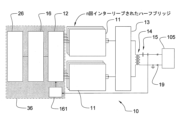
本発明による電圧波形生成器の可能なシステムアーキテクチャを図2~図6に示す。図4は、最も基本的なスキームである。 Possible system architectures of voltage waveform generators according to the invention are shown in FIGS. 2-6. Figure 4 is the most basic scheme.
図2~図6を参照すると、電圧波形生成器10の出力端子19における所望の出力電圧は、パルス幅変調(PWM)制御の降圧セル11によって生成される。1つのそのような降圧セル11の可能な実装形態は、図7に示すようにアクティブにスイッチング可能な半導体スイッチ111を備えるハーフブリッジである。PWMは、典型的には、PWM生成器12、例えば、フィールドプログラマブルゲートアレイ(FPGA)によって生成される。電流を分配するために、複数の降圧セル11が並列に配置され得る。降圧セルのPWMは、リップル電流を低減し、実効スイッチング周波数fsw_effを上昇させるために、位相がずれて適用される(すなわち、インターリーブ動作)。降圧セル出力電圧は、高調波成分を除去するためにフィルタ13によってフィルタリングされる。
Referring to FIGS. 2-6, the desired output voltage at the
降圧セル電流共有は、降圧セルのコイル電流を測定し、電流が降圧セル間で均等に分配されるように、降圧セルを制御するPWM信号を調整することによって対処され得る。 Buck cell current sharing may be addressed by measuring the buck cell coil current and adjusting the PWM signal controlling the buck cells so that the current is evenly distributed between the buck cells.
変圧器14は、フィルタリングされた降圧セル出力電圧を変圧器の巻数比によってシステムに必要なレベルに上昇させている(低下させることもできる)。基板テーブル電位のDCバイアス電圧は、変圧器14の後のDC遮断キャパシタ15上に自動的に配置される。これは、変圧器14および降圧セル11に対する電圧ストレスを低減している。DC遮断キャパシタ15はまた、(例えば、プラズマのDC電位による)二次DC電流が変圧器を飽和させることを防止している。一次側における変圧器の飽和の防止は、例えば、コントローラ16によって、電流を測定し、変圧器の一次側におけるDC電圧を防止するために、生成されたPWM信号を調整することによって行われ得る。(オプション)のEMCフィルタ17が、基準に準拠するために、ABVGで発生した高周波成分をフィルタリングするために使用される。
The
より複雑な変圧器構成により、3つ以上のインターリーブされたハーフブリッジ(降圧セル11)を並列に配置することが可能である。 With more complex transformer configurations, it is possible to place three or more interleaved half-bridges (step-down cells 11) in parallel.
降圧セル電源における適切な電圧レベル、および所望のバイアス電圧の適切な電圧レベルにより、変圧器14を省略することが可能である。可能な降圧セル電圧レベルは、利用可能な半導体スイッチ111によって制限されることに留意されたい。
With appropriate voltage levels on the step-down cell power supply and appropriate voltage levels of the desired bias voltage,
変圧器の出力側は、ユーザが変圧器の巻数比と、したがって出力電圧範囲とを選択することを可能にする複数のタブを備えることができる。代替的には、ABVGは、複数の出力電圧設定を切り替えるための(内部)リレーを備えることができる。 The output side of the transformer may be provided with a plurality of tabs that allow the user to select the transformer turns ratio and therefore the output voltage range. Alternatively, the ABVG may be equipped with an (internal) relay to switch between multiple output voltage settings.
利用可能な半導体スイッチ111のスイッチング速度には制限がある。これは、より高い帯域幅を有することができる線形増幅器18によって解消され得る。ABVG帯域幅を増加させるために、いくらかの効率損失を犠牲にして、いくらかより高い高調波(典型的にはより少ないエネルギーを含む)を発生させるために線形電力増幅器18が追加され得る。ABVG内のコントローラ16は、PWM生成器12と(オプションの)線形電力増幅器18の両方を制御することができる。コントローラ16によって供給されるデジタル出力は、線形電力増幅器18に供給される前に、D/A変換器28を介してアナログ信号に変換される。
There are limits to the switching speed of available semiconductor switches 111. This can be overcome by a
図4における変圧器のDCバイアス/飽和を防止するために、DC遮断キャパシタ15が設けられる。代替的には、変圧器の一次側は、グランドの代わりにスプリットバス(降圧セル11と共有される)に接続され得る。図4におけるEMCフィルタは、オプションである。
A
複数の降圧セルを並列に動作させるための位相シフトされたPWM信号の発生によって、実効スイッチング周波数fsw_eff(fsw_eff=n*2*1つの降圧セルのスイッチング周波数)が上昇され得る。このトポロジーにより、対応するPWM信号の発生によって任意の波形が合成され得る。繰り返し波形が、そのフーリエ成分の合計として見られ得る。経験則として、このABVGトポロジーによって生成され得る最高周波数は、fsw_eff/5である。作成され得るフーリエ成分が多いほど、所望の電圧波形がより良く再現される。このトポロジーにより、約fsw_eff/5までのフーリエ成分を有する任意の波形が生成され得る。 By generating a phase-shifted PWM signal to operate multiple buck cells in parallel, the effective switching frequency f sw_eff (f sw_eff =n*2*switching frequency of one buck cell) can be increased. With this topology, any waveform can be synthesized by generating a corresponding PWM signal. A repeating waveform can be viewed as the sum of its Fourier components. As a rule of thumb, the highest frequency that can be produced by this ABVG topology is f sw_eff /5. The more Fourier components that can be created, the better the desired voltage waveform will be reproduced. With this topology, arbitrary waveforms with Fourier components up to about f sw_eff /5 can be generated.
このトポロジーにより、降圧セルは、最先端の最高クラスの半導体スイッチ(これを書いている時点でGaN HEMTデバイス)を用いて実装され得る。これらのスイッチは、非常に高速に切り替わることができ、結果として、低いターンオンおよびターンオフ損失と、したがって高効率とをもたらす。効率をさらに高めるために、変換器は、ゼロ電圧スイッチング(ZVS)において動作され得る。これは、降圧セルインダクタ112のインダクタンス値を減少させることによって行われ得る。
This topology allows buck cells to be implemented using state-of-the-art, best-in-class semiconductor switches (GaN HEMT devices at the time of this writing). These switches can switch very quickly, resulting in low turn-on and turn-off losses and therefore high efficiency. To further increase efficiency, the converter can be operated in zero voltage switching (ZVS). This may be done by decreasing the inductance value of step-down
内部センサとオプションの外部センサとを有する閉ループ電圧制御システムを実装することは、電圧波形の生成と再現性とをさらに改善することができる。バイアス電圧の直接制御、したがってイオン速度の直接制御は、最新技術によって示されるものと比較して、システムレベルにおいてはるかにより低い(おそらく、最大で一桁低い)電力消費を結果としてもたらすことができる。 Implementing a closed loop voltage control system with internal sensors and optional external sensors can further improve voltage waveform generation and repeatability. Direct control of bias voltage, and thus of ion velocity, can result in much lower (perhaps up to an order of magnitude lower) power consumption at the system level compared to that exhibited by the state of the art.
プラズマチャンバ102内のプロセスに応じて、高精度(例えば、原子層エッチング)または高電力(例えば、スパッタリング)が必要とされる。スパッタリングのような高電力プロセスでは、より低い精度が許容される可能性がある。結果として、ABVGコントローラ16は、そのような動作モードにおいて、より少ない帯域幅を必要とし、より低い実効スイッチング周波数を可能にする。一態様によれば、コントローラ16は、ABVGの異なる動作モードを選択することを可能にするように構成された制御プログラムまたは方法を用いて実装される。例として、図8のフローチャートは、可能な選択を示す。有利には、少なくとも2つの、有利には少なくとも3つの動作モードが、異なる電力レベルおよび/またはスイッチング周波数の異なるレベルに対応して、コントローラ16において実装され、低電力、高電力、および場合によっては中電力が、それぞれ低スイッチング周波数、高スイッチング周波数、または中スイッチング周波数に対応する。動作モードは、少なくとも2つの電圧レベルおよび/または少なくとも2つの電流レベル間の選択に基づいて選択され得る。
Depending on the process within
低電圧を選択することは、より低いバス電圧(降圧セルの電源電圧)をもたらす。低電流を選択することは、ABVG保護回路のより低い電流レベルをもたらす。この保護回路は、2つの方法において動作するように構成され得る。第1の場合、図9を参照すると、保護回路161は、(変圧器14の二次側における)出力電流を測定するように構成された過電流検出回路として構成され、電流が高すぎると、保護回路161は、ABVG電力段を無効にするために無効信号を発し、エラーが発生される。第2の場合、図10を参照すると、保護回路162は、(例えば、変圧器14の二次側における)出力電流を測定するように構成された電流制限回路として構成され、電流が高すぎると、保護回路162は、出力電流を低減/制限する出力電圧を低下させる(典型的な実験室電源のような挙動)。
Selecting a lower voltage results in a lower bus voltage (power supply voltage of the buck cell). Selecting a low current results in a lower current level for the ABVG protection circuit. This protection circuit can be configured to operate in two ways. In the first case, referring to FIG. 9, the
図9および図10を参照すると、コントローラ16、PWM生成器12、波形生成器26、D/Aコンバータ(例えば、線形増幅器用)、制御(フィードバック)ループ、および保護回路161、162は、1つまたは複数のフィールドプログラマブルゲートアレイ(FPGA)36に統合され得ることに留意することが便利である。波形生成器26は、オプションでプレディストーションを用いて、出力電圧設定値を提供するように構成され得る。コントローラ16は、フィードバックを伴う制御ループを備えることができる。
9 and 10, the
狭いイオンエネルギー分布(IED)では、基板電圧は、有利には、図11に示すように、tONの間、平坦であるべきである。これを達成するために、基板(およびホルダ)の容量性充電は、有利には、tONの間、ABVG出力電圧dVOUT/dtを調整することによって補償される。tON中の平坦な基板電圧は、tON中の連続的なイオン電流と、したがって、連続的なABVG出力電流とをもたらす。これは、ABVG出力電圧を測定するように構成され、tONの間にdVOUT/dtを調整するように構成されたコントローラに結合された電流測定ユニットを設けることによって、ABVGによって取得され得る。これは、ABVG出力電圧を調整するために使用される間接的に測定されたプロセスパラメータの一例である。これは、プロセスパフォーマンスを改善し、この場合、IEDのより良好な制御をもたらす。図12を参照すると、基板電圧、結果として生じるABVG出力電流、および準最適な場合に目標基板電圧を達成するために必要なABVG出力電圧が示されている。 In a narrow ion energy distribution (IED), the substrate voltage should advantageously be flat during t ON , as shown in FIG. To achieve this, capacitive charging of the substrate (and holder) is advantageously compensated for by adjusting the ABVG output voltage dV OUT /dt during t ON . A flat substrate voltage during t ON results in continuous ion current during t ON and therefore continuous ABVG output current. This can be obtained by the ABVG by providing a current measurement unit coupled to a controller configured to measure the ABVG output voltage and configured to adjust dV OUT /dt during t ON . This is an example of an indirectly measured process parameter used to adjust the ABVG output voltage. This improves process performance and in this case results in better control of the IED. Referring to FIG. 12, the substrate voltage, the resulting ABVG output current, and the ABVG output voltage required to achieve the target substrate voltage in the suboptimal case are shown.
他の例において、ABVGは、イオンフラックスまたはIEDを測定し、ABVG出力電圧(設定値)の制御のためにこの情報を使用するように構成される。 In other examples, the ABVG is configured to measure ion flux or IED and use this information for control of the ABVG output voltage (setpoint).
一態様において、ABVGおよび/またはプラズマ処理装置を動作させる方法は、複数の動作モードを含む制御プログラムの実装を含む。第1の動作モードは、高電力モードに対応することができる。第2の動作モードは、高精度モードに対応することができる。複数の動作モードは、異なるスイッチング周波数、異なる出力電圧、異なる出力電流のうちの1つまたは組合せによって区別することができる。 In one aspect, a method of operating an ABVG and/or plasma processing apparatus includes implementing a control program that includes multiple modes of operation. The first mode of operation may correspond to a high power mode. The second mode of operation may correspond to a high precision mode. Multiple operating modes can be distinguished by one or a combination of different switching frequencies, different output voltages, different output currents.
高電力モードに対応する第1の動作モードは、有利には、スイッチング周波数が低く、出力電圧および電流が高い、例えば、それらが最大レベルにあるモードに対応する。低いスイッチング周波数は、有利には、低いスイッチング損失をもたらし、次に、より高い伝導損失が許容され得、したがって、出力電流レベルが増加され得る。スイッチング損失を制限するために高い出力電圧を使用する場合、低いスイッチング周波数が有利である。 The first operating mode, corresponding to a high power mode, advantageously corresponds to a mode in which the switching frequency is low and the output voltage and current are high, eg, they are at their maximum level. Lower switching frequencies advantageously result in lower switching losses, which in turn may allow higher conduction losses and thus increase output current levels. Low switching frequencies are advantageous when using high output voltages to limit switching losses.
高精度モードに対応する第2の動作モードは、様々な方法において取得され得る。あるいは、これらの方法の各々は、異なる動作モードであり得る。第1のオプションにおいて、出力電流は、制限され得、より低い伝導損失をもたらす。より低い伝導損失は、第1のモードに対してスイッチング周波数を上昇させることを可能にし得る。このオプションにおいて、スイッチング周波数および出力電圧は、高レベルに維持され得る。高いスイッチング周波数は、高い帯域幅と、したがってより高い精度とをもたらす。 The second mode of operation, corresponding to the high precision mode, can be obtained in various ways. Alternatively, each of these methods may be a different mode of operation. In the first option, the output current can be limited, resulting in lower conduction losses. Lower conduction losses may allow increasing the switching frequency for the first mode. In this option, the switching frequency and output voltage can be maintained at high levels. Higher switching frequencies result in higher bandwidth and therefore higher accuracy.
第2のモードに関する第2のオプションにおいて、出力電圧が制限される。第1のモードに対して出力電圧を低下させることは、スイッチング損失を低減し、それは、第1のモードに対してスイッチング周波数を上昇させることを可能にし得る。したがって、より高い精度が得られ得る。 In a second option for the second mode, the output voltage is limited. Reducing the output voltage for the first mode reduces switching losses, which may allow increasing the switching frequency for the first mode. Therefore, higher accuracy may be obtained.
第2のモードに関する第3のオプションにおいて、出力電圧と出力電流の両方が、第1のモード(高電力モード)に対して制限される。これは、(より低い電流による)伝導損失と(より低い出力電圧による)スイッチング損失の両方を低減し、したがって、スイッチング周波数を最大レベルまで上昇させることを可能にする。このオプションは、最高精度の動作モードをもたらし得る。 In a third option for the second mode, both the output voltage and the output current are limited relative to the first mode (high power mode). This reduces both conduction losses (due to lower current) and switching losses (due to lower output voltage), thus making it possible to increase the switching frequency to maximum levels. This option may provide the highest precision mode of operation.
第3のオプションにおいて、出力電力は、最低であり得る。第1および/または第2のオプションにおいて、出力電力は、第1のモードにおいて得られる出力電力と第3のオプションにおいて得られる出力電力との間の中間であり得る。 In the third option, the output power may be the lowest. In the first and/or second option, the output power may be intermediate between the output power obtained in the first mode and the output power obtained in the third option.
装置は、オペレータが異なる動作モード間で選択することを可能にするユーザインターフェースを備え得る。第1から第3のオプションのいずれかが、ABVGの明確な動作モードとして制御ユニット内に実装され得る。 The device may include a user interface that allows an operator to select between different modes of operation. Any of the first to third options may be implemented within the control unit as a distinct mode of operation of the ABVG.
フィードバックが装置内に実装され得る。フィードバックは、電流および/または電圧フィードバックに基づき得る。有利には、フィードバック制御ループは、イオンエネルギー密度および/または基板を通るイオン電流などの測定されたプロセスパラメータに基づき得る。 Feedback may be implemented within the device. Feedback may be based on current and/or voltage feedback. Advantageously, the feedback control loop may be based on measured process parameters such as ion energy density and/or ion current through the substrate.
10 ABVG、電圧波形生成器
11 降圧セル
12 PWM生成器
13 フィルタ
14 変圧器
15 DC遮断キャパシタ
16 コントローラ、ABVGコントローラ
17 EMCフィルタ
18 線形増幅器、線形電力増幅器
19 出力端子
26 波形生成器
28 D/A変換器
36 フィールドプログラマブルゲートアレイ(FPGA)
100 誘導結合プラズマ(ICP)装置
101 基板
102 プラズマ反応器、プラズマチャンバ
103 プラズマ
104 プラズマ形成ガス
105 ステージまたはプラットフォーム
107 誘導コイル
108 誘導管
109 前駆体
111 半導体スイッチ
112 降圧セルインダクタ
120 RF電源
121 マッチングネットワーク
130 システムホストコントローラ
161 保護回路
162 保護回路
10 ABVG, voltage waveform generator
11 Step-down cell
12 PWM generator
13 Filter
14 Transformer
15 DC cut-off capacitor
16 Controller, ABVG Controller
17 EMC filter
18 Linear amplifier, linear power amplifier
19 Output terminal
26 Waveform Generator
28 D/A converter
36 Field Programmable Gate Array (FPGA)
100 Inductively coupled plasma (ICP) equipment
101 Board
102 Plasma reactor, plasma chamber
103 Plasma
104 Plasma forming gas
105 stage or platform
107 Induction coil
108 Guidance tube
109 Precursor
111 Semiconductor switch
112 Buck Cell Inductor
120 RF power supply
121 Matching Network
130 System host controller
161 Protection circuit
162 Protection circuit
Claims (23)
処理されるべき基板(101)を支持するための処理プラットフォーム(105)と、
前記処理プラットフォーム(105)に電気的に結合された出力(19)を備える電圧波形生成器(10)と
を備えるプラズマ処理装置(100)であって、
前記電圧波形生成器(10)が、
並列に配置され、前記出力(19)に結合された複数の第1の降圧変換器(11)であって、前記第1の降圧変換器(11)がアクティブにスイッチング可能な半導体スイッチ(111)を備える、複数の第1の降圧変換器(11)と、
パルス幅変調信号を介して前記アクティブにスイッチング可能な半導体スイッチ(111)を動作させるように構成された制御ユニット(16)と
を備え、
前記制御ユニット(16)が、前記複数の第1の降圧変換器(11)をインターリーブ方式において動作させるように構成される、
ことを特徴とする、プラズマ処理装置(100)。 means for generating plasma;
a processing platform (105) for supporting a substrate (101) to be processed;
a voltage waveform generator (10) having an output (19) electrically coupled to the processing platform (105), the plasma processing apparatus (100) comprising:
The voltage waveform generator (10)
a plurality of first step-down converters (11) arranged in parallel and coupled to said output (19), said first step-down converters (11) comprising an actively switchable semiconductor switch (111); a plurality of first step-down converters (11);
a control unit (16) configured to operate the actively switchable semiconductor switch (111) via a pulse width modulated signal;
the control unit (16) is configured to operate the plurality of first step-down converters (11) in an interleaved manner;
A plasma processing apparatus (100) characterized by:
前記制御ユニットが、パルス幅変調信号を介して前記第2の降圧変換器の前記アクティブにスイッチング可能な半導体スイッチを動作するように構成され、前記複数の第2の降圧変換器をインターリーブ方式において動作させるように構成され、
前記複数の第1の降圧変換器および前記複数の第2の降圧変換器が並列に配置された、
請求項1または2に記載のプラズマ処理装置。 the voltage waveform generator comprising a plurality of second step-down converters arranged in parallel and coupled to the output, the second step-down converters comprising an actively switchable semiconductor switch;
The control unit is configured to operate the actively switchable semiconductor switches of the second step-down converters via a pulse width modulated signal, and operates the plurality of second step-down converters in an interleaved manner. configured to
the plurality of first step-down converters and the plurality of second step-down converters are arranged in parallel;
3. The plasma processing apparatus according to claim 1 or 2.
Applications Claiming Priority (5)
| Application Number | Priority Date | Filing Date | Title |
|---|---|---|---|
| EP18205472 | 2018-11-09 | ||
| EP18205472.6 | 2018-11-09 | ||
| NL2022222 | 2018-12-17 | ||
| NL2022222A NL2022222B1 (en) | 2018-12-17 | 2018-12-17 | Voltage waveform generator for plasma processing apparatuses |
| PCT/EP2019/080405 WO2020094723A1 (en) | 2018-11-09 | 2019-11-06 | Voltage waveform generator for plasma processing apparatuses |
Publications (2)
| Publication Number | Publication Date |
|---|---|
| JP2022506833A JP2022506833A (en) | 2022-01-17 |
| JP7444875B2 true JP7444875B2 (en) | 2024-03-06 |
Family
ID=68424911
Family Applications (1)
| Application Number | Title | Priority Date | Filing Date |
|---|---|---|---|
| JP2021524442A Active JP7444875B2 (en) | 2018-11-09 | 2019-11-06 | Voltage waveform generator for plasma processing equipment |
Country Status (7)
| Country | Link |
|---|---|
| US (1) | US11968771B2 (en) |
| EP (1) | EP3878002B1 (en) |
| JP (1) | JP7444875B2 (en) |
| KR (1) | KR102815626B1 (en) |
| CN (1) | CN113169019A (en) |
| TW (1) | TWI863939B (en) |
| WO (1) | WO2020094723A1 (en) |
Families Citing this family (5)
| Publication number | Priority date | Publication date | Assignee | Title |
|---|---|---|---|---|
| US11545943B2 (en) | 2020-12-04 | 2023-01-03 | Mks Instruments, Inc. | Switched capacitor modulator |
| JP2024536715A (en) * | 2021-09-08 | 2024-10-08 | ラム リサーチ コーポレーション | Hybrid Frequency Plasma Source |
| US12505982B2 (en) | 2021-09-09 | 2025-12-23 | Applied Materials, Inc. | Method and apparatus for digital control of ion energy distribution in a plasma |
| US12567572B2 (en) | 2023-07-11 | 2026-03-03 | Advanced Energy Industries, Inc. | Plasma behaviors predicted by current measurements during asymmetric bias waveform application |
| KR102850760B1 (en) * | 2024-05-09 | 2025-08-28 | 엠케이에스코리아 유한회사 | Asymmetric Multi-Level Control of Pulse Generator |
Citations (4)
| Publication number | Priority date | Publication date | Assignee | Title |
|---|---|---|---|---|
| JP2012050296A (en) | 2010-08-30 | 2012-03-08 | Daihen Corp | High frequency power supply device |
| US20130009479A1 (en) | 2007-02-28 | 2013-01-10 | Netlogic Microsystems, Inc. | Multi-Phase Power System with Redundancy |
| JP2017079127A (en) | 2015-10-20 | 2017-04-27 | 国立研究開発法人産業技術総合研究所 | Inductively coupled plasma generating apparatus, self bias applying apparatus, plasma processing apparatus, plasma generating method, and self bias applying method |
| US20170291245A1 (en) | 2016-04-12 | 2017-10-12 | Hypertherm, Inc. | Systems and methods for providing power for plasma arc cutting |
Family Cites Families (5)
| Publication number | Priority date | Publication date | Assignee | Title |
|---|---|---|---|---|
| KR100314358B1 (en) * | 1993-11-30 | 2001-12-28 | 리챠드 에이.뉴베리 | Switch-Mode Power Supplies for Bridged Linear Amplifiers |
| US6031746A (en) * | 1998-09-04 | 2000-02-29 | General Electric Company | Switching amplifier for generating continuous arbitrary waveforms for magnetic resonance imaging coils |
| US6979980B1 (en) | 2004-08-24 | 2005-12-27 | Advanced Energy Industries, Inc. | Soft switching interleaved power converter |
| US9287086B2 (en) | 2010-04-26 | 2016-03-15 | Advanced Energy Industries, Inc. | System, method and apparatus for controlling ion energy distribution |
| US20110315916A1 (en) | 2010-06-29 | 2011-12-29 | Dow Global Technologies Inc. | Curable composition |
-
2019
- 2019-11-06 US US17/291,976 patent/US11968771B2/en active Active
- 2019-11-06 EP EP19797298.7A patent/EP3878002B1/en active Active
- 2019-11-06 KR KR1020217017577A patent/KR102815626B1/en active Active
- 2019-11-06 WO PCT/EP2019/080405 patent/WO2020094723A1/en not_active Ceased
- 2019-11-06 JP JP2021524442A patent/JP7444875B2/en active Active
- 2019-11-06 CN CN201980071810.7A patent/CN113169019A/en active Pending
- 2019-11-07 TW TW108140420A patent/TWI863939B/en active
Patent Citations (4)
| Publication number | Priority date | Publication date | Assignee | Title |
|---|---|---|---|---|
| US20130009479A1 (en) | 2007-02-28 | 2013-01-10 | Netlogic Microsystems, Inc. | Multi-Phase Power System with Redundancy |
| JP2012050296A (en) | 2010-08-30 | 2012-03-08 | Daihen Corp | High frequency power supply device |
| JP2017079127A (en) | 2015-10-20 | 2017-04-27 | 国立研究開発法人産業技術総合研究所 | Inductively coupled plasma generating apparatus, self bias applying apparatus, plasma processing apparatus, plasma generating method, and self bias applying method |
| US20170291245A1 (en) | 2016-04-12 | 2017-10-12 | Hypertherm, Inc. | Systems and methods for providing power for plasma arc cutting |
Also Published As
| Publication number | Publication date |
|---|---|
| EP3878002A1 (en) | 2021-09-15 |
| KR20210090228A (en) | 2021-07-19 |
| WO2020094723A1 (en) | 2020-05-14 |
| US11968771B2 (en) | 2024-04-23 |
| TWI863939B (en) | 2024-12-01 |
| EP3878002C0 (en) | 2023-06-07 |
| JP2022506833A (en) | 2022-01-17 |
| EP3878002B1 (en) | 2023-06-07 |
| TW202035747A (en) | 2020-10-01 |
| CN113169019A (en) | 2021-07-23 |
| US20220013330A1 (en) | 2022-01-13 |
| KR102815626B1 (en) | 2025-06-02 |
Similar Documents
| Publication | Publication Date | Title |
|---|---|---|
| JP7444875B2 (en) | Voltage waveform generator for plasma processing equipment | |
| US11875972B2 (en) | Voltage waveform generator for plasma processing apparatuses | |
| TWI775843B (en) | Piecewise rf power systems and methods for supplying pre-distorted rf bias voltage signals to an electrode in a processing chamber | |
| TWI551026B (en) | Dielectric barrier discharge power system and method of generating dielectric barrier discharge | |
| US6642661B2 (en) | Method to affect spatial distribution of harmonic generation in a capacitive discharge reactor | |
| US20110259851A1 (en) | System, method and apparatus for controlling ion energy distribution | |
| US20120262064A1 (en) | Radio Frequency Power Delivery System | |
| KR20230036115A (en) | Voltage Waveform Generator for Plasma Auxiliary Processing Devices | |
| KR20240136438A (en) | Bias supply control and data processing | |
| SG182969A1 (en) | Distributed power arrangements for localizing power delivery | |
| JP2026504050A (en) | Capacitance as a control of the power applied by the bias power supply | |
| KR20230036116A (en) | Voltage Waveform Generator for Plasma Auxiliary Processing Devices | |
| JP4773165B2 (en) | High frequency power supply | |
| JP5284971B2 (en) | RF plasma generator and method for distributing constant power to a plasma load | |
| NL2022222B1 (en) | Voltage waveform generator for plasma processing apparatuses | |
| KR102756076B1 (en) | Radio frequency pulse power apparatus and its operating mehtod | |
| Estrin et al. | Soft-switched pulsed bias plasma supply system | |
| US12586761B2 (en) | Fast tuning radio frequency (RF) matching network | |
| KR100970376B1 (en) | The voltage output circuit of modulator | |
| WO2024249397A1 (en) | System and associated methods for controlling radiofrequency power delivery to plasma processing chamber | |
| WO2025168530A1 (en) | Radio frequency drive generator for plasma sources | |
| WO2006133132A2 (en) | Combinations of plasma production devices and method and rf driver circuits with adjustable duty cycle | |
| KR20250107831A (en) | Voltage waveform generator for ion energy control in plasma processing | |
| HK1081334A1 (en) | Power factor correction circuit and method of varying switching frequency | |
| HK1081334B (en) | Power factor correction circuit and method of varying switching frequency |
Legal Events
| Date | Code | Title | Description |
|---|---|---|---|
| A711 | Notification of change in applicant |
Free format text: JAPANESE INTERMEDIATE CODE: A711 Effective date: 20211020 |
|
| A621 | Written request for application examination |
Free format text: JAPANESE INTERMEDIATE CODE: A621 Effective date: 20221021 |
|
| A977 | Report on retrieval |
Free format text: JAPANESE INTERMEDIATE CODE: A971007 Effective date: 20230816 |
|
| A131 | Notification of reasons for refusal |
Free format text: JAPANESE INTERMEDIATE CODE: A131 Effective date: 20230828 |
|
| A521 | Request for written amendment filed |
Free format text: JAPANESE INTERMEDIATE CODE: A523 Effective date: 20231128 |
|
| TRDD | Decision of grant or rejection written | ||
| A01 | Written decision to grant a patent or to grant a registration (utility model) |
Free format text: JAPANESE INTERMEDIATE CODE: A01 Effective date: 20240129 |
|
| A61 | First payment of annual fees (during grant procedure) |
Free format text: JAPANESE INTERMEDIATE CODE: A61 Effective date: 20240222 |
|
| R150 | Certificate of patent or registration of utility model |
Ref document number: 7444875 Country of ref document: JP Free format text: JAPANESE INTERMEDIATE CODE: R150 |