JP7429797B2 - Coating equipment and its coating method - Google Patents
Coating equipment and its coating method Download PDFInfo
- Publication number
- JP7429797B2 JP7429797B2 JP2022548224A JP2022548224A JP7429797B2 JP 7429797 B2 JP7429797 B2 JP 7429797B2 JP 2022548224 A JP2022548224 A JP 2022548224A JP 2022548224 A JP2022548224 A JP 2022548224A JP 7429797 B2 JP7429797 B2 JP 7429797B2
- Authority
- JP
- Japan
- Prior art keywords
- coating
- monomer
- electrode
- plasma
- source
- Prior art date
- Legal status (The legal status is an assumption and is not a legal conclusion. Google has not performed a legal analysis and makes no representation as to the accuracy of the status listed.)
- Active
Links
- 238000000576 coating method Methods 0.000 title claims description 286
- 239000011248 coating agent Substances 0.000 title claims description 248
- 239000000178 monomer Substances 0.000 claims description 290
- 230000005284 excitation Effects 0.000 claims description 276
- 239000000758 substrate Substances 0.000 claims description 230
- 239000000463 material Substances 0.000 claims description 199
- 239000010408 film Substances 0.000 claims description 175
- 238000006243 chemical reaction Methods 0.000 claims description 161
- 239000007789 gas Substances 0.000 claims description 96
- 230000033001 locomotion Effects 0.000 claims description 52
- 229920006254 polymer film Polymers 0.000 claims description 46
- 230000008093 supporting effect Effects 0.000 claims description 44
- 239000010409 thin film Substances 0.000 claims description 43
- -1 methyl (perfluorocyclohexyl)acrylate Chemical group 0.000 claims description 17
- URLKBWYHVLBVBO-UHFFFAOYSA-N Para-Xylene Chemical group CC1=CC=C(C)C=C1 URLKBWYHVLBVBO-UHFFFAOYSA-N 0.000 claims description 8
- 238000007599 discharging Methods 0.000 claims description 8
- 150000002894 organic compounds Chemical class 0.000 claims description 8
- MYRTYDVEIRVNKP-UHFFFAOYSA-N 1,2-Divinylbenzene Chemical compound C=CC1=CC=CC=C1C=C MYRTYDVEIRVNKP-UHFFFAOYSA-N 0.000 claims description 6
- KUDUQBURMYMBIJ-UHFFFAOYSA-N 2-prop-2-enoyloxyethyl prop-2-enoate Chemical compound C=CC(=O)OCCOC(=O)C=C KUDUQBURMYMBIJ-UHFFFAOYSA-N 0.000 claims description 6
- 150000001875 compounds Chemical class 0.000 claims description 6
- 239000001257 hydrogen Substances 0.000 claims description 6
- 229910052739 hydrogen Inorganic materials 0.000 claims description 6
- 125000004432 carbon atom Chemical group C* 0.000 claims description 5
- 229910052736 halogen Inorganic materials 0.000 claims description 5
- 150000002367 halogens Chemical class 0.000 claims description 5
- 125000005842 heteroatom Chemical group 0.000 claims description 5
- ZDQNWDNMNKSMHI-UHFFFAOYSA-N 1-[2-(2-prop-2-enoyloxypropoxy)propoxy]propan-2-yl prop-2-enoate Chemical compound C=CC(=O)OC(C)COC(C)COCC(C)OC(=O)C=C ZDQNWDNMNKSMHI-UHFFFAOYSA-N 0.000 claims description 4
- NIXOWILDQLNWCW-UHFFFAOYSA-M Acrylate Chemical compound [O-]C(=O)C=C NIXOWILDQLNWCW-UHFFFAOYSA-M 0.000 claims description 4
- 150000001336 alkenes Chemical class 0.000 claims description 4
- 150000001345 alkine derivatives Chemical class 0.000 claims description 4
- 238000004891 communication Methods 0.000 claims description 4
- 239000011521 glass Substances 0.000 claims description 4
- YDKNBNOOCSNPNS-UHFFFAOYSA-N methyl 1,3-benzoxazole-2-carboxylate Chemical compound C1=CC=C2OC(C(=O)OC)=NC2=C1 YDKNBNOOCSNPNS-UHFFFAOYSA-N 0.000 claims description 4
- 229920001223 polyethylene glycol Polymers 0.000 claims description 4
- 229920002635 polyurethane Polymers 0.000 claims description 4
- 239000004814 polyurethane Substances 0.000 claims description 4
- 230000001105 regulatory effect Effects 0.000 claims description 4
- 229920006395 saturated elastomer Polymers 0.000 claims description 4
- SAMJGBVVQUEMGC-UHFFFAOYSA-N 1-ethenoxy-2-(2-ethenoxyethoxy)ethane Chemical compound C=COCCOCCOC=C SAMJGBVVQUEMGC-UHFFFAOYSA-N 0.000 claims description 3
- SMZOUWXMTYCWNB-UHFFFAOYSA-N 2-(2-methoxy-5-methylphenyl)ethanamine Chemical compound COC1=CC=C(C)C=C1CCN SMZOUWXMTYCWNB-UHFFFAOYSA-N 0.000 claims description 3
- NIXOWILDQLNWCW-UHFFFAOYSA-N 2-Propenoic acid Natural products OC(=O)C=C NIXOWILDQLNWCW-UHFFFAOYSA-N 0.000 claims description 3
- PRDFNJUWGIQQBW-UHFFFAOYSA-N 3,3,3-trifluoroprop-1-yne Chemical group FC(F)(F)C#C PRDFNJUWGIQQBW-UHFFFAOYSA-N 0.000 claims description 3
- SWTZSHBOMGAQKX-UHFFFAOYSA-N 3,3,4,4,5,5,6,6,7,7,8,8,9,9,10,10,11,11,12,12,13,13,14,14,14-pentacosafluorotetradecyl prop-2-enoate Chemical compound FC(F)(F)C(F)(F)C(F)(F)C(F)(F)C(F)(F)C(F)(F)C(F)(F)C(F)(F)C(F)(F)C(F)(F)C(F)(F)C(F)(F)CCOC(=O)C=C SWTZSHBOMGAQKX-UHFFFAOYSA-N 0.000 claims description 3
- FIHBHSQYSYVZQE-UHFFFAOYSA-N 6-prop-2-enoyloxyhexyl prop-2-enoate Chemical compound C=CC(=O)OCCCCCCOC(=O)C=C FIHBHSQYSYVZQE-UHFFFAOYSA-N 0.000 claims description 3
- 239000004593 Epoxy Substances 0.000 claims description 3
- 230000003213 activating effect Effects 0.000 claims description 3
- 230000005540 biological transmission Effects 0.000 claims description 3
- 239000000919 ceramic Substances 0.000 claims description 3
- 150000002431 hydrogen Chemical class 0.000 claims description 3
- 150000002678 macrocyclic compounds Chemical class 0.000 claims description 3
- 239000002184 metal Substances 0.000 claims description 3
- 229910052751 metal Inorganic materials 0.000 claims description 3
- 239000004065 semiconductor Substances 0.000 claims description 3
- 125000000547 substituted alkyl group Chemical group 0.000 claims description 3
- GTELLNMUWNJXMQ-UHFFFAOYSA-N 2-ethyl-2-(hydroxymethyl)propane-1,3-diol;prop-2-enoic acid Chemical class OC(=O)C=C.OC(=O)C=C.OC(=O)C=C.CCC(CO)(CO)CO GTELLNMUWNJXMQ-UHFFFAOYSA-N 0.000 claims description 2
- VPKQPPJQTZJZDB-UHFFFAOYSA-N 3,3,4,4,5,5,6,6,7,7,8,8,8-tridecafluorooctyl prop-2-enoate Chemical compound FC(F)(F)C(F)(F)C(F)(F)C(F)(F)C(F)(F)C(F)(F)CCOC(=O)C=C VPKQPPJQTZJZDB-UHFFFAOYSA-N 0.000 claims description 2
- ZLQGITSKRNWIOT-UHFFFAOYSA-N 5-(dimethylamino)furan-2-carbaldehyde Chemical compound CN(C)C1=CC=C(C=O)O1 ZLQGITSKRNWIOT-UHFFFAOYSA-N 0.000 claims description 2
- UFHFLCQGNIYNRP-UHFFFAOYSA-N Hydrogen Chemical compound [H][H] UFHFLCQGNIYNRP-UHFFFAOYSA-N 0.000 claims description 2
- 125000000217 alkyl group Chemical group 0.000 claims description 2
- 125000001188 haloalkyl group Chemical group 0.000 claims description 2
- 125000001165 hydrophobic group Chemical group 0.000 claims description 2
- 239000004753 textile Substances 0.000 claims description 2
- XTKBMZQCDBHHKY-UHFFFAOYSA-N 1-ethynyl-4-(trifluoromethyl)benzene Chemical compound FC(F)(F)C1=CC=C(C#C)C=C1 XTKBMZQCDBHHKY-UHFFFAOYSA-N 0.000 claims 1
- RPDBRTLKDYJCCE-UHFFFAOYSA-N [4,4,5,5,6,6,7,7,8,9,9,9-dodecafluoro-2-hydroxy-8-(trifluoromethyl)nonyl] 2-methylprop-2-enoate Chemical compound CC(=C)C(=O)OCC(O)CC(F)(F)C(F)(F)C(F)(F)C(F)(F)C(F)(C(F)(F)F)C(F)(F)F RPDBRTLKDYJCCE-UHFFFAOYSA-N 0.000 claims 1
- 125000001495 ethyl group Chemical group [H]C([H])([H])C([H])([H])* 0.000 claims 1
- JRZJOMJEPLMPRA-UHFFFAOYSA-N olefin Natural products CCCCCCCC=C JRZJOMJEPLMPRA-UHFFFAOYSA-N 0.000 claims 1
- 239000004033 plastic Substances 0.000 claims 1
- 229920003023 plastic Polymers 0.000 claims 1
- 239000010410 layer Substances 0.000 description 221
- 238000010586 diagram Methods 0.000 description 33
- 238000000034 method Methods 0.000 description 30
- 239000002994 raw material Substances 0.000 description 29
- 239000002243 precursor Substances 0.000 description 24
- 230000008901 benefit Effects 0.000 description 20
- 239000011247 coating layer Substances 0.000 description 16
- 238000006116 polymerization reaction Methods 0.000 description 12
- 238000004519 manufacturing process Methods 0.000 description 11
- 230000008569 process Effects 0.000 description 11
- 238000000354 decomposition reaction Methods 0.000 description 10
- 239000002120 nanofilm Substances 0.000 description 9
- 238000003860 storage Methods 0.000 description 9
- 238000004132 cross linking Methods 0.000 description 8
- 238000000151 deposition Methods 0.000 description 8
- 239000007788 liquid Substances 0.000 description 8
- 230000002209 hydrophobic effect Effects 0.000 description 7
- 239000000203 mixture Substances 0.000 description 7
- IJGRMHOSHXDMSA-UHFFFAOYSA-N Atomic nitrogen Chemical compound N#N IJGRMHOSHXDMSA-UHFFFAOYSA-N 0.000 description 6
- 230000009471 action Effects 0.000 description 6
- 230000008878 coupling Effects 0.000 description 6
- 238000010168 coupling process Methods 0.000 description 6
- 238000005859 coupling reaction Methods 0.000 description 6
- 238000010438 heat treatment Methods 0.000 description 6
- 239000000126 substance Substances 0.000 description 6
- 229930195735 unsaturated hydrocarbon Natural products 0.000 description 6
- 239000006200 vaporizer Substances 0.000 description 6
- 238000005229 chemical vapour deposition Methods 0.000 description 5
- 239000001307 helium Substances 0.000 description 5
- 229910052734 helium Inorganic materials 0.000 description 5
- SWQJXJOGLNCZEY-UHFFFAOYSA-N helium atom Chemical compound [He] SWQJXJOGLNCZEY-UHFFFAOYSA-N 0.000 description 5
- 229920000642 polymer Polymers 0.000 description 5
- 229920001296 polysiloxane Polymers 0.000 description 5
- 230000001681 protective effect Effects 0.000 description 5
- GETTZEONDQJALK-UHFFFAOYSA-N (trifluoromethyl)benzene Chemical compound FC(F)(F)C1=CC=CC=C1 GETTZEONDQJALK-UHFFFAOYSA-N 0.000 description 4
- OKTJSMMVPCPJKN-UHFFFAOYSA-N Carbon Chemical compound [C] OKTJSMMVPCPJKN-UHFFFAOYSA-N 0.000 description 4
- 238000013459 approach Methods 0.000 description 4
- 229910052799 carbon Inorganic materials 0.000 description 4
- 230000008021 deposition Effects 0.000 description 4
- 230000005684 electric field Effects 0.000 description 4
- 230000001976 improved effect Effects 0.000 description 4
- 238000011068 loading method Methods 0.000 description 4
- 229910052757 nitrogen Inorganic materials 0.000 description 4
- 230000002093 peripheral effect Effects 0.000 description 4
- 238000009832 plasma treatment Methods 0.000 description 4
- 238000000623 plasma-assisted chemical vapour deposition Methods 0.000 description 4
- 239000005871 repellent Substances 0.000 description 4
- 230000002459 sustained effect Effects 0.000 description 4
- RYGMFSIKBFXOCR-UHFFFAOYSA-N Copper Chemical compound [Cu] RYGMFSIKBFXOCR-UHFFFAOYSA-N 0.000 description 3
- 239000012159 carrier gas Substances 0.000 description 3
- 230000001276 controlling effect Effects 0.000 description 3
- 229910052802 copper Inorganic materials 0.000 description 3
- 239000010949 copper Substances 0.000 description 3
- 230000006378 damage Effects 0.000 description 3
- 125000004386 diacrylate group Chemical group 0.000 description 3
- 238000010892 electric spark Methods 0.000 description 3
- 238000000605 extraction Methods 0.000 description 3
- 230000006870 function Effects 0.000 description 3
- 229930195733 hydrocarbon Natural products 0.000 description 3
- 150000002430 hydrocarbons Chemical class 0.000 description 3
- 230000001939 inductive effect Effects 0.000 description 3
- 239000011261 inert gas Substances 0.000 description 3
- 230000003287 optical effect Effects 0.000 description 3
- 239000000843 powder Substances 0.000 description 3
- XLYOFNOQVPJJNP-UHFFFAOYSA-N water Substances O XLYOFNOQVPJJNP-UHFFFAOYSA-N 0.000 description 3
- GYUPEJSTJSFVRR-UHFFFAOYSA-N 3,3,4,4,5,5,6,6,6-nonafluorohexyl prop-2-enoate Chemical compound FC(F)(F)C(F)(F)C(F)(F)C(F)(F)CCOC(=O)C=C GYUPEJSTJSFVRR-UHFFFAOYSA-N 0.000 description 2
- GRJRKPMIRMSBNK-UHFFFAOYSA-N 3,3,4,4,5,5,6,6,7,7,8,8,8-tridecafluorooctan-1-ol Chemical compound OCCC(F)(F)C(F)(F)C(F)(F)C(F)(F)C(F)(F)C(F)(F)F GRJRKPMIRMSBNK-UHFFFAOYSA-N 0.000 description 2
- XKRFYHLGVUSROY-UHFFFAOYSA-N Argon Chemical compound [Ar] XKRFYHLGVUSROY-UHFFFAOYSA-N 0.000 description 2
- 239000004215 Carbon black (E152) Substances 0.000 description 2
- LYCAIKOWRPUZTN-UHFFFAOYSA-N Ethylene glycol Chemical compound OCCO LYCAIKOWRPUZTN-UHFFFAOYSA-N 0.000 description 2
- BAPJBEWLBFYGME-UHFFFAOYSA-N Methyl acrylate Chemical compound COC(=O)C=C BAPJBEWLBFYGME-UHFFFAOYSA-N 0.000 description 2
- 239000002202 Polyethylene glycol Substances 0.000 description 2
- 210000000746 body region Anatomy 0.000 description 2
- 239000004020 conductor Substances 0.000 description 2
- 238000010276 construction Methods 0.000 description 2
- 230000007797 corrosion Effects 0.000 description 2
- 238000005260 corrosion Methods 0.000 description 2
- 238000006073 displacement reaction Methods 0.000 description 2
- 230000000694 effects Effects 0.000 description 2
- 239000003822 epoxy resin Substances 0.000 description 2
- 239000000835 fiber Substances 0.000 description 2
- 125000001153 fluoro group Chemical group F* 0.000 description 2
- 238000009413 insulation Methods 0.000 description 2
- JEIPFZHSYJVQDO-UHFFFAOYSA-N iron(III) oxide Inorganic materials O=[Fe]O[Fe]=O JEIPFZHSYJVQDO-UHFFFAOYSA-N 0.000 description 2
- 229920000052 poly(p-xylylene) Polymers 0.000 description 2
- 229920000647 polyepoxide Polymers 0.000 description 2
- 230000002940 repellent Effects 0.000 description 2
- 230000033764 rhythmic process Effects 0.000 description 2
- 238000012360 testing method Methods 0.000 description 2
- 230000008016 vaporization Effects 0.000 description 2
- VRBFTYUMFJWSJY-UHFFFAOYSA-N 28804-46-8 Chemical compound ClC1CC(C=C2)=CC=C2C(Cl)CC2=CC=C1C=C2 VRBFTYUMFJWSJY-UHFFFAOYSA-N 0.000 description 1
- FQHLOOOXLDQLPF-UHFFFAOYSA-N 3,3,4,4,5,5,6,6,7,7,8,8,9,9,10,10,11,11,12,12,12-henicosafluorododecyl 2-methylprop-2-enoate Chemical compound CC(=C)C(=O)OCCC(F)(F)C(F)(F)C(F)(F)C(F)(F)C(F)(F)C(F)(F)C(F)(F)C(F)(F)C(F)(F)C(F)(F)F FQHLOOOXLDQLPF-UHFFFAOYSA-N 0.000 description 1
- UYNXMRWOFAEXOW-UHFFFAOYSA-N 4,4,5,5,5-pentafluoropentyl prop-2-enoate Chemical compound FC(F)(F)C(F)(F)CCCOC(=O)C=C UYNXMRWOFAEXOW-UHFFFAOYSA-N 0.000 description 1
- FAIDUPDWTLBHFO-UHFFFAOYSA-N 4,4,5,5,6,6,7,7,8,8,9,9,10,10,11,11,12,12,13,13,13-henicosafluorotridecyl prop-2-enoate Chemical compound [H]C([H])=C([H])C(=O)OC([H])([H])C([H])([H])C([H])([H])C(F)(F)C(F)(F)C(F)(F)C(F)(F)C(F)(F)C(F)(F)C(F)(F)C(F)(F)C(F)(F)C(F)(F)F FAIDUPDWTLBHFO-UHFFFAOYSA-N 0.000 description 1
- HRPVXLWXLXDGHG-UHFFFAOYSA-N Acrylamide Chemical compound NC(=O)C=C HRPVXLWXLXDGHG-UHFFFAOYSA-N 0.000 description 1
- 239000004642 Polyimide Substances 0.000 description 1
- 229910008072 Si-N-Si Inorganic materials 0.000 description 1
- 229910002808 Si–O–Si Inorganic materials 0.000 description 1
- 230000004913 activation Effects 0.000 description 1
- 239000000853 adhesive Substances 0.000 description 1
- 230000001070 adhesive effect Effects 0.000 description 1
- 230000032683 aging Effects 0.000 description 1
- 238000013019 agitation Methods 0.000 description 1
- 150000001335 aliphatic alkanes Chemical class 0.000 description 1
- 229910052786 argon Inorganic materials 0.000 description 1
- 239000000969 carrier Substances 0.000 description 1
- 230000015556 catabolic process Effects 0.000 description 1
- 230000008859 change Effects 0.000 description 1
- 239000002131 composite material Substances 0.000 description 1
- 229920001577 copolymer Polymers 0.000 description 1
- 125000004122 cyclic group Chemical group 0.000 description 1
- 230000007423 decrease Effects 0.000 description 1
- 230000003247 decreasing effect Effects 0.000 description 1
- 238000009792 diffusion process Methods 0.000 description 1
- 150000002148 esters Chemical class 0.000 description 1
- 238000002474 experimental method Methods 0.000 description 1
- 239000004744 fabric Substances 0.000 description 1
- NBVXSUQYWXRMNV-UHFFFAOYSA-N fluoromethane Chemical class FC NBVXSUQYWXRMNV-UHFFFAOYSA-N 0.000 description 1
- 238000013467 fragmentation Methods 0.000 description 1
- 238000006062 fragmentation reaction Methods 0.000 description 1
- 125000000524 functional group Chemical group 0.000 description 1
- 125000005843 halogen group Chemical group 0.000 description 1
- 125000004435 hydrogen atom Chemical group [H]* 0.000 description 1
- 229920001600 hydrophobic polymer Polymers 0.000 description 1
- 230000005661 hydrophobic surface Effects 0.000 description 1
- WGCNASOHLSPBMP-UHFFFAOYSA-N hydroxyacetaldehyde Natural products OCC=O WGCNASOHLSPBMP-UHFFFAOYSA-N 0.000 description 1
- 230000006872 improvement Effects 0.000 description 1
- 238000002347 injection Methods 0.000 description 1
- 239000007924 injection Substances 0.000 description 1
- 229910010272 inorganic material Inorganic materials 0.000 description 1
- 239000011147 inorganic material Substances 0.000 description 1
- 239000011810 insulating material Substances 0.000 description 1
- 150000002739 metals Chemical class 0.000 description 1
- 238000002156 mixing Methods 0.000 description 1
- 238000012986 modification Methods 0.000 description 1
- 230000004048 modification Effects 0.000 description 1
- 239000011368 organic material Substances 0.000 description 1
- 229920001721 polyimide Polymers 0.000 description 1
- 230000000379 polymerizing effect Effects 0.000 description 1
- 230000002265 prevention Effects 0.000 description 1
- 230000009467 reduction Effects 0.000 description 1
- 239000002356 single layer Substances 0.000 description 1
- 239000002002 slurry Substances 0.000 description 1
- 239000007787 solid Substances 0.000 description 1
- 239000000243 solution Substances 0.000 description 1
- 239000007921 spray Substances 0.000 description 1
- 230000003068 static effect Effects 0.000 description 1
- 239000002345 surface coating layer Substances 0.000 description 1
- TXEYQDLBPFQVAA-UHFFFAOYSA-N tetrafluoromethane Chemical compound FC(F)(F)F TXEYQDLBPFQVAA-UHFFFAOYSA-N 0.000 description 1
- 238000012546 transfer Methods 0.000 description 1
- 238000009834 vaporization Methods 0.000 description 1
- 239000002699 waste material Substances 0.000 description 1
- 238000004078 waterproofing Methods 0.000 description 1
Images


Classifications
-
- C—CHEMISTRY; METALLURGY
- C23—COATING METALLIC MATERIAL; COATING MATERIAL WITH METALLIC MATERIAL; CHEMICAL SURFACE TREATMENT; DIFFUSION TREATMENT OF METALLIC MATERIAL; COATING BY VACUUM EVAPORATION, BY SPUTTERING, BY ION IMPLANTATION OR BY CHEMICAL VAPOUR DEPOSITION, IN GENERAL; INHIBITING CORROSION OF METALLIC MATERIAL OR INCRUSTATION IN GENERAL
- C23C—COATING METALLIC MATERIAL; COATING MATERIAL WITH METALLIC MATERIAL; SURFACE TREATMENT OF METALLIC MATERIAL BY DIFFUSION INTO THE SURFACE, BY CHEMICAL CONVERSION OR SUBSTITUTION; COATING BY VACUUM EVAPORATION, BY SPUTTERING, BY ION IMPLANTATION OR BY CHEMICAL VAPOUR DEPOSITION, IN GENERAL
- C23C16/00—Chemical coating by decomposition of gaseous compounds, without leaving reaction products of surface material in the coating, i.e. chemical vapour deposition [CVD] processes
- C23C16/44—Chemical coating by decomposition of gaseous compounds, without leaving reaction products of surface material in the coating, i.e. chemical vapour deposition [CVD] processes characterised by the method of coating
- C23C16/50—Chemical coating by decomposition of gaseous compounds, without leaving reaction products of surface material in the coating, i.e. chemical vapour deposition [CVD] processes characterised by the method of coating using electric discharges
- C23C16/513—Chemical coating by decomposition of gaseous compounds, without leaving reaction products of surface material in the coating, i.e. chemical vapour deposition [CVD] processes characterised by the method of coating using electric discharges using plasma jets
-
- C—CHEMISTRY; METALLURGY
- C23—COATING METALLIC MATERIAL; COATING MATERIAL WITH METALLIC MATERIAL; CHEMICAL SURFACE TREATMENT; DIFFUSION TREATMENT OF METALLIC MATERIAL; COATING BY VACUUM EVAPORATION, BY SPUTTERING, BY ION IMPLANTATION OR BY CHEMICAL VAPOUR DEPOSITION, IN GENERAL; INHIBITING CORROSION OF METALLIC MATERIAL OR INCRUSTATION IN GENERAL
- C23C—COATING METALLIC MATERIAL; COATING MATERIAL WITH METALLIC MATERIAL; SURFACE TREATMENT OF METALLIC MATERIAL BY DIFFUSION INTO THE SURFACE, BY CHEMICAL CONVERSION OR SUBSTITUTION; COATING BY VACUUM EVAPORATION, BY SPUTTERING, BY ION IMPLANTATION OR BY CHEMICAL VAPOUR DEPOSITION, IN GENERAL
- C23C16/00—Chemical coating by decomposition of gaseous compounds, without leaving reaction products of surface material in the coating, i.e. chemical vapour deposition [CVD] processes
- C23C16/44—Chemical coating by decomposition of gaseous compounds, without leaving reaction products of surface material in the coating, i.e. chemical vapour deposition [CVD] processes characterised by the method of coating
- C23C16/50—Chemical coating by decomposition of gaseous compounds, without leaving reaction products of surface material in the coating, i.e. chemical vapour deposition [CVD] processes characterised by the method of coating using electric discharges
- C23C16/515—Chemical coating by decomposition of gaseous compounds, without leaving reaction products of surface material in the coating, i.e. chemical vapour deposition [CVD] processes characterised by the method of coating using electric discharges using pulsed discharges
-
- C—CHEMISTRY; METALLURGY
- C23—COATING METALLIC MATERIAL; COATING MATERIAL WITH METALLIC MATERIAL; CHEMICAL SURFACE TREATMENT; DIFFUSION TREATMENT OF METALLIC MATERIAL; COATING BY VACUUM EVAPORATION, BY SPUTTERING, BY ION IMPLANTATION OR BY CHEMICAL VAPOUR DEPOSITION, IN GENERAL; INHIBITING CORROSION OF METALLIC MATERIAL OR INCRUSTATION IN GENERAL
- C23C—COATING METALLIC MATERIAL; COATING MATERIAL WITH METALLIC MATERIAL; SURFACE TREATMENT OF METALLIC MATERIAL BY DIFFUSION INTO THE SURFACE, BY CHEMICAL CONVERSION OR SUBSTITUTION; COATING BY VACUUM EVAPORATION, BY SPUTTERING, BY ION IMPLANTATION OR BY CHEMICAL VAPOUR DEPOSITION, IN GENERAL
- C23C16/00—Chemical coating by decomposition of gaseous compounds, without leaving reaction products of surface material in the coating, i.e. chemical vapour deposition [CVD] processes
- C23C16/44—Chemical coating by decomposition of gaseous compounds, without leaving reaction products of surface material in the coating, i.e. chemical vapour deposition [CVD] processes characterised by the method of coating
- C23C16/455—Chemical coating by decomposition of gaseous compounds, without leaving reaction products of surface material in the coating, i.e. chemical vapour deposition [CVD] processes characterised by the method of coating characterised by the method used for introducing gases into reaction chamber or for modifying gas flows in reaction chamber
- C23C16/45502—Flow conditions in reaction chamber
- C23C16/45508—Radial flow
-
- C—CHEMISTRY; METALLURGY
- C23—COATING METALLIC MATERIAL; COATING MATERIAL WITH METALLIC MATERIAL; CHEMICAL SURFACE TREATMENT; DIFFUSION TREATMENT OF METALLIC MATERIAL; COATING BY VACUUM EVAPORATION, BY SPUTTERING, BY ION IMPLANTATION OR BY CHEMICAL VAPOUR DEPOSITION, IN GENERAL; INHIBITING CORROSION OF METALLIC MATERIAL OR INCRUSTATION IN GENERAL
- C23C—COATING METALLIC MATERIAL; COATING MATERIAL WITH METALLIC MATERIAL; SURFACE TREATMENT OF METALLIC MATERIAL BY DIFFUSION INTO THE SURFACE, BY CHEMICAL CONVERSION OR SUBSTITUTION; COATING BY VACUUM EVAPORATION, BY SPUTTERING, BY ION IMPLANTATION OR BY CHEMICAL VAPOUR DEPOSITION, IN GENERAL
- C23C16/00—Chemical coating by decomposition of gaseous compounds, without leaving reaction products of surface material in the coating, i.e. chemical vapour deposition [CVD] processes
- C23C16/44—Chemical coating by decomposition of gaseous compounds, without leaving reaction products of surface material in the coating, i.e. chemical vapour deposition [CVD] processes characterised by the method of coating
- C23C16/458—Chemical coating by decomposition of gaseous compounds, without leaving reaction products of surface material in the coating, i.e. chemical vapour deposition [CVD] processes characterised by the method of coating characterised by the method used for supporting substrates in the reaction chamber
- C23C16/4582—Rigid and flat substrates, e.g. plates or discs
- C23C16/4583—Rigid and flat substrates, e.g. plates or discs the substrate being supported substantially horizontally
- C23C16/4584—Rigid and flat substrates, e.g. plates or discs the substrate being supported substantially horizontally the substrate being rotated
-
- C—CHEMISTRY; METALLURGY
- C23—COATING METALLIC MATERIAL; COATING MATERIAL WITH METALLIC MATERIAL; CHEMICAL SURFACE TREATMENT; DIFFUSION TREATMENT OF METALLIC MATERIAL; COATING BY VACUUM EVAPORATION, BY SPUTTERING, BY ION IMPLANTATION OR BY CHEMICAL VAPOUR DEPOSITION, IN GENERAL; INHIBITING CORROSION OF METALLIC MATERIAL OR INCRUSTATION IN GENERAL
- C23C—COATING METALLIC MATERIAL; COATING MATERIAL WITH METALLIC MATERIAL; SURFACE TREATMENT OF METALLIC MATERIAL BY DIFFUSION INTO THE SURFACE, BY CHEMICAL CONVERSION OR SUBSTITUTION; COATING BY VACUUM EVAPORATION, BY SPUTTERING, BY ION IMPLANTATION OR BY CHEMICAL VAPOUR DEPOSITION, IN GENERAL
- C23C16/00—Chemical coating by decomposition of gaseous compounds, without leaving reaction products of surface material in the coating, i.e. chemical vapour deposition [CVD] processes
- C23C16/44—Chemical coating by decomposition of gaseous compounds, without leaving reaction products of surface material in the coating, i.e. chemical vapour deposition [CVD] processes characterised by the method of coating
- C23C16/50—Chemical coating by decomposition of gaseous compounds, without leaving reaction products of surface material in the coating, i.e. chemical vapour deposition [CVD] processes characterised by the method of coating using electric discharges
- C23C16/505—Chemical coating by decomposition of gaseous compounds, without leaving reaction products of surface material in the coating, i.e. chemical vapour deposition [CVD] processes characterised by the method of coating using electric discharges using radio frequency discharges
- C23C16/509—Chemical coating by decomposition of gaseous compounds, without leaving reaction products of surface material in the coating, i.e. chemical vapour deposition [CVD] processes characterised by the method of coating using electric discharges using radio frequency discharges using internal electrodes
- C23C16/5093—Coaxial electrodes
-
- H—ELECTRICITY
- H01—ELECTRIC ELEMENTS
- H01J—ELECTRIC DISCHARGE TUBES OR DISCHARGE LAMPS
- H01J37/00—Discharge tubes with provision for introducing objects or material to be exposed to the discharge, e.g. for the purpose of examination or processing thereof
- H01J37/32—Gas-filled discharge tubes
- H01J37/32009—Arrangements for generation of plasma specially adapted for examination or treatment of objects, e.g. plasma sources
- H01J37/32357—Generation remote from the workpiece, e.g. down-stream
-
- H—ELECTRICITY
- H01—ELECTRIC ELEMENTS
- H01J—ELECTRIC DISCHARGE TUBES OR DISCHARGE LAMPS
- H01J37/00—Discharge tubes with provision for introducing objects or material to be exposed to the discharge, e.g. for the purpose of examination or processing thereof
- H01J37/32—Gas-filled discharge tubes
- H01J37/32431—Constructional details of the reactor
- H01J37/3244—Gas supply means
- H01J37/32449—Gas control, e.g. control of the gas flow
-
- H—ELECTRICITY
- H01—ELECTRIC ELEMENTS
- H01J—ELECTRIC DISCHARGE TUBES OR DISCHARGE LAMPS
- H01J37/00—Discharge tubes with provision for introducing objects or material to be exposed to the discharge, e.g. for the purpose of examination or processing thereof
- H01J37/32—Gas-filled discharge tubes
- H01J37/32431—Constructional details of the reactor
- H01J37/32532—Electrodes
- H01J37/32568—Relative arrangement or disposition of electrodes; moving means
-
- H—ELECTRICITY
- H01—ELECTRIC ELEMENTS
- H01J—ELECTRIC DISCHARGE TUBES OR DISCHARGE LAMPS
- H01J37/00—Discharge tubes with provision for introducing objects or material to be exposed to the discharge, e.g. for the purpose of examination or processing thereof
- H01J37/32—Gas-filled discharge tubes
- H01J37/32431—Constructional details of the reactor
- H01J37/32733—Means for moving the material to be treated
- H01J37/32752—Means for moving the material to be treated for moving the material across the discharge
- H01J37/32761—Continuous moving
- H01J37/32779—Continuous moving of batches of workpieces
-
- B—PERFORMING OPERATIONS; TRANSPORTING
- B05—SPRAYING OR ATOMISING IN GENERAL; APPLYING FLUENT MATERIALS TO SURFACES, IN GENERAL
- B05D—PROCESSES FOR APPLYING FLUENT MATERIALS TO SURFACES, IN GENERAL
- B05D1/00—Processes for applying liquids or other fluent materials
- B05D1/60—Deposition of organic layers from vapour phase
-
- B—PERFORMING OPERATIONS; TRANSPORTING
- B05—SPRAYING OR ATOMISING IN GENERAL; APPLYING FLUENT MATERIALS TO SURFACES, IN GENERAL
- B05D—PROCESSES FOR APPLYING FLUENT MATERIALS TO SURFACES, IN GENERAL
- B05D1/00—Processes for applying liquids or other fluent materials
- B05D1/62—Plasma-deposition of organic layers
-
- B—PERFORMING OPERATIONS; TRANSPORTING
- B05—SPRAYING OR ATOMISING IN GENERAL; APPLYING FLUENT MATERIALS TO SURFACES, IN GENERAL
- B05D—PROCESSES FOR APPLYING FLUENT MATERIALS TO SURFACES, IN GENERAL
- B05D2401/00—Form of the coating product, e.g. solution, water dispersion, powders or the like
- B05D2401/30—Form of the coating product, e.g. solution, water dispersion, powders or the like the coating being applied in other forms than involving eliminable solvent, diluent or dispersant
- B05D2401/33—Form of the coating product, e.g. solution, water dispersion, powders or the like the coating being applied in other forms than involving eliminable solvent, diluent or dispersant applied as vapours polymerising in situ
-
- B—PERFORMING OPERATIONS; TRANSPORTING
- B05—SPRAYING OR ATOMISING IN GENERAL; APPLYING FLUENT MATERIALS TO SURFACES, IN GENERAL
- B05D—PROCESSES FOR APPLYING FLUENT MATERIALS TO SURFACES, IN GENERAL
- B05D2502/00—Acrylic polymers
Description
本発明は堆積式コーティングに関して、特に、コーティング機器及びコーティング方法に関し、前記方法はフィルム層を基材に付与し形成し、前記基材はフィルム層形成材料の放出ソースとプラズマ励起ソースとの間に設けられることで、フィルム層成形工程において前記フィルム層形成材料の過度分解を防止する。 FIELD OF THE INVENTION The present invention relates to depositional coatings, and more particularly to coating equipment and methods for applying and forming a film layer on a substrate, the substrate being between an emission source of film layer-forming material and a plasma excitation source. By providing this, excessive decomposition of the film layer forming material is prevented in the film layer forming process.
コーティング機器は、基材の表面にポリマーコート層又は薄膜を形成するように配置され、前記基材の製造材料は、金属、ガラス、セラミック、ポリマー、繊維、粉末及び半導体を含むが、これらに限定されず、前記基材の多種の性能、例えば、疎水性、親水性、疎油性、防錆、防カビ、防湿、電気/熱伝導率、生物医学、光学、摩擦性能を向上させる。 The coating equipment is arranged to form a polymer coat layer or thin film on the surface of the substrate, and the materials of manufacture of the substrate include, but are not limited to, metals, glasses, ceramics, polymers, fibers, powders, and semiconductors. It improves various properties of the substrate, such as hydrophobicity, hydrophilicity, oleophobicity, rust prevention, mold resistance, moisture resistance, electrical/thermal conductivity, biomedical, optical, and frictional performance.
典型的なコーティング機器はプラズマ体化学気相成長法PECVD (Plasma Enhanced Chemical Vapor Deposition)を利用し、ガスフィルム層形成材料を真空室に導入するように製造され、前記真空室には1つ又は複数の前記基材が配置され、これによって、前記基材の表面にポリマーコート層を形成する。より具体的に、前記ガスフィルム層形成材料は有機材料、有機シリコーン材料、無機材料、及び以上の組み合わせを含むが、これらに限定されず、電気エネルギーをモノマーに放出することで、多種の活性前駆体を生成し、前記基材をプラズマ化するように活性化されるモノマーガス又はモノマー蒸気である。そして、活性前駆体と前記モノマーとの間は反応が生じ、又は活性前駆体自体は反応が生じて、その後、ポリマー薄膜は前記基材の表面に堆積形成される。 Typical coating equipment utilizes plasma enhanced chemical vapor deposition (PECVD) and is manufactured to introduce the gas film layer-forming material into a vacuum chamber that includes one or more vacuum chambers. of the substrate is disposed, thereby forming a polymer coat layer on the surface of the substrate. More specifically, the gas film layer forming material includes, but is not limited to, organic materials, organic silicone materials, inorganic materials, and combinations of the above, and by releasing electrical energy into the monomer, various active precursors can be formed. The monomer gas or vapor is activated to produce a plasma and turn the substrate into a plasma. A reaction then occurs between the active precursor and the monomer, or the active precursor itself, and a thin polymer film is then deposited on the surface of the substrate.
モノマーは活性前駆体を生成するように励起されるべきであるが、モノマーはプラズマ励起媒体において過度に曝されると、モノマーの過度分解を招致し、堆積速度及びポリマーフィルム層の均一性に悪影響を及ぼす。 Although the monomer should be excited to produce active precursors, overexposure of the monomer in the plasma excitation medium can lead to excessive decomposition of the monomer and negatively affect the deposition rate and uniformity of the polymer film layer. effect.
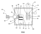
図1Aに示すように、従来のコーティング機器はチャンバ体1と、フィルム層形成材料をチャンバ体1に導入するためのフィルム層形成材料の放出ソース2と、フィルム層形成材料に電気エネルギーを印加し、前記フィルム層形成材料を励起するためのプラズマ励起ソース3と、を含む。図面に示すように、1つ又は複数の基材4は前記プラズマ励起ソース3の相対する電極の間に設けられる。前記フィルム層形成材料は前記プラズマ励起ソース3の相対する電極の間の空間に分散し、励起過程を通過することで、活性前駆体を生成する。フィルム層形成材料は前記プラズマ励起ソース3の作用で励起され、前記プラズマ励起ソース3に配置される前記基材4に堆積すべきであるため、フィルム層形成材料には過度分解が発生する恐れがある。また、前記基材4の、前記プラズマ励起ソース3の電極の間での曝露も、前記基材4に対する損傷を招致する恐れがある。
As shown in FIG. 1A, the conventional coating equipment includes a
図1Bに示すように、別の従来のコーティング機器はチャンバ体1、フィルム層形成材料の放出ソース2と、フィルム層形成材料の前記放出ソース2とコーティング対象である基材4との間に設けられるプラズマ励起ソース3とを含む。コーティング方法期間で、前記基材4に達する前、活性前駆体を生成するための励起過程を実行するように、フィルム層形成材料は前記プラズマ励起ソース3の相対する電極の間の空間を通過する必要がある。
As shown in FIG. 1B, another conventional coating device is provided with a
名称が「前駆体を、遠位基材を塗装するための励起媒体に気化する」である米国特許番号US7,968,154B2、及び名称が「フィルム層形成材料を少なくとも1つの基材に付与する」である米国特許番号US8,029,872B2は、気化モノマーソース及びプラズマ励起媒体を含むコーティング機器を開示している。前記基材及び気化されたモノマーソースはそれぞれプラズマ励起媒体の対向する両側に位置し、気化モノマーソースはプラズマ励起媒体を通過してから、プラズマ励起媒体の対向側の基材の表面に堆積し、ポリマーフィルム層を形成する。従って、気化されたモノマーはプラズマ励起媒体を通過した場合のみ、基材の表面に堆積できる。プラズマ励起媒体は大部分の気化モノマーを比較的長い時間内で分解させ、気化モノマーを過度に分解させる恐れがあるため、形成したフィルム層は、気化されたフィルム層形成材料の化学性質を保持し難い。 US Pat. US Pat. No. 8,029,872B2, published in 1999, discloses a coating equipment that includes a vaporized monomer source and a plasma excitation medium. the substrate and the vaporized monomer source are each located on opposite sides of the plasma excitation medium, the vaporized monomer source passing through the plasma excitation medium before being deposited on the surface of the substrate on the opposite side of the plasma excitation medium; Form a polymer film layer. Therefore, the vaporized monomer can only be deposited on the surface of the substrate if it passes through the plasma excitation medium. Because the plasma excitation medium decomposes most of the vaporized monomer within a relatively long time and may cause excessive decomposition of the vaporized monomer, the formed film layer retains the chemical properties of the vaporized film layer-forming material. hard.
名称が「マルチソース低電力低温プラズマ体重合コーティング装置及び方法」である米国特許出願番号US16/095179は、コーティング装置を開示し、前記コーティング装置は、単一の大面積、大電力高周波放電源の代わりとして、複数の小面積、低電力の光源高周波放電を組み合わせる。ところが、前記方法は依然として、ある程度でモノマーの化学モノマー構成を過度に破壊し、形成されたポリマーフィルム層の品質が不十分であり、装置の構成が複雑で、且つ組立が困難である。 United States Patent Application No. US 16/095179, entitled "Multi-Source Low Power Low Temperature Plasma Polymerization Coating Apparatus and Method," discloses a coating apparatus which includes a single large area, high power radio frequency discharge source. As an alternative, multiple small-area, low-power light sources combine high-frequency discharges. However, the method still causes excessive destruction of the chemical monomer composition of the monomers to some extent, the quality of the formed polymer film layer is insufficient, the equipment configuration is complicated, and the assembly is difficult.
本発明の主な利点はコーティング機器及びコーティング方法を提供することにあり、プラズマ体重合コーティング方法期間で、フィルム層形成材料を過度に破壊することないように、基材の表面にはフィルム層が形成される。 The main advantage of the present invention is to provide a coating equipment and a coating method in which a film layer is formed on the surface of the substrate so as not to excessively destroy the film layer forming material during the plasma polymerization coating method. It is formed.
本発明の別の利点はコーティング機器及びコーティング方法を提供することにあり、コーティング対象である前記基材は、フィルム層形成材料をチャンバ体に導入するためのモノマー放出ソースと、フィルム層形成材料を励起するためのプラズマ励起ソースとの間に配置されることで、ガスモノマー又は気化モノマーであるフィルム層形成材料は、基材に達する前、前記プラズマ励起ソースを通過する必要がなくなるため、フィルム層形成材料の過度分解を低減させる。 Another advantage of the present invention is to provide coating equipment and methods, wherein the substrate to be coated includes a monomer release source for introducing the film layer forming material into the chamber body; By being placed between the plasma excitation source for excitation, the film layer forming material, which is a gaseous or vaporized monomer, does not need to pass through the plasma excitation source before reaching the substrate. Reduces excessive decomposition of forming materials.
本発明の別の利点はコーティング機器及びコーティング方法を提供することにあり、少なくとも一部のフィルム層形成材料がプラズマ励起ソースに達する前、基材を位置決める領域に達するように、コーティング対象である基材は、前記プラズマ励起ソースより、前記モノマー放出ソースまでの距離が小さい位置に配置され、これによって、基材に達する前に、全てのフィルム層形成材料がいずれもプラズマ励起ソースを通過する必要がなくなる。 Another advantage of the present invention is to provide a coating apparatus and a coating method in which at least some of the film layer-forming material reaches an area for positioning a substrate before reaching a plasma excitation source. The substrate is positioned at a smaller distance from the plasma excitation source to the monomer emission source such that all film layer forming material must pass through the plasma excitation source before reaching the substrate. disappears.
本発明の別の利点はコーティング機器及びコーティング方法を提供することにあり、前記モノマー放出ソースと、前記基材を支持するための支持フレームとを含み、前記プラズマ励起ソースの構造は所望の活性前駆体の間の反応レベルを保持でき、これは、所定割合のモノマーが前記プラズマ励起ソースに達することによって発生したものであり、別の部分のモノマーはまだ活性前駆体に分解していなく、基材の表面に形成されたポリマーフィルム層の品質を向上させる。 Another advantage of the present invention is to provide coating equipment and methods including the monomer emitting source and a support frame for supporting the substrate, wherein the structure of the plasma excitation source is configured to provide a desired active precursor. The reaction level between the substrate and the substrate can be maintained because a certain proportion of the monomer reaches the plasma excitation source and another portion of the monomer has not yet decomposed into active precursors. improve the quality of the polymer film layer formed on the surface of the
本発明の別の利点はコーティング機器及びコーティング方法を提供することにあり、いくつかの実施形態によれば、コーティング対象である基材は前記支持フレームに支持され、前記支持フレームはモノマー放出ソースとプラズマ励起ソースとの間を移動し、前記基材と前記プラズマ励起ソースとの間の距離を調節し、基材の表面に堆積形成されるポリマー材料の構成成分を制御して調節する。 Another advantage of the present invention is to provide coating equipment and methods, in which, according to some embodiments, the substrate to be coated is supported on the support frame, and the support frame is connected to a monomer release source. and a plasma excitation source to adjust the distance between the substrate and the plasma excitation source to control and adjust the composition of the polymeric material deposited on the surface of the substrate.
本発明の別の利点はコーティング機器及びコーティング方法を提供することにあり、いくつかの実施形態によれば、前記プラズマ励起ソースは前記チャンバ体の反応チャンバの略中央位置に設けられ、また、複数の前記基材は前記プラズマ励起ソースの周囲に配置され、前記フィルム層形成材料は、前記チャンバ体の内壁に隣接する位置での前記モノマー放出ソースに放出され、径方向で反応チャンバに分散され、プラズマ励起ソースに達する前、基材を配置する領域を通過する必要がある。 Another advantage of the present invention is to provide a coating apparatus and method, in which, according to some embodiments, the plasma excitation source is provided at a substantially central position of the reaction chamber of the chamber body, and a plurality of the substrate of is disposed around the plasma excitation source, the film layer-forming material being ejected into the monomer emitting source at a location adjacent to an inner wall of the chamber body and distributed radially into the reaction chamber; Before reaching the plasma excitation source, it is necessary to pass through an area where the substrate is to be placed.
本発明の別の利点はコーティング機器及びコーティング方法を提供することにあり、いくつかの実施形態によれば、前記基材を支持するための前記支持フレームは、前記反応チャンバにおいて前記プラズマ励起ソースに対して回転する回転台を含むように実施され、前記基材と前記プラズマ励起ソースとの間の相対位置を変更することで、前記反応チャンバに分散された気化フィルム層形成材料に対する撹拌の役割を果たし、前記基材の表面に形成されるポリマーフィルム層の均一性を向上させる。 Another advantage of the present invention is to provide a coating apparatus and method, in which, according to some embodiments, the support frame for supporting the substrate is connected to the plasma excitation source in the reaction chamber. and a rotating table that rotates against the substrate and changes the relative position between the substrate and the plasma excitation source to provide agitation for the vaporized film layer-forming material dispersed in the reaction chamber. As a result, the uniformity of the polymer film layer formed on the surface of the substrate is improved.
本発明の別の利点はコーティング機器及びコーティング方法を提供することにあり、いくつかの実施形態によれば、前記基材とフィルム層形成材料の前記モノマー放出ソースとの間の相対運動は制御可能であるため、前記プラズマ励起ソースの励起によって影響されずに、前記フィルム層形成材料の、前記基材に達する量を調節し、活性前駆体とモノマーとは十分に反応でき、高品質のポリマーフィルム層は前記基材の表面に堆積する。 Another advantage of the present invention is to provide coating equipment and methods in which, according to some embodiments, relative movement between the substrate and the monomer release source of the film layering material is controllable. Therefore, the amount of the film layer-forming material reaching the substrate can be adjusted without being influenced by the excitation of the plasma excitation source, and the active precursor and monomer can fully react, producing a high quality polymer film. A layer is deposited on the surface of the substrate.
本発明の別の利点はコーティング機器及びコーティング方法を提供することにあり、いくつかの実施形態によれば、前記基材と前記プラズマ励起ソースとの間の相対運動は制御可能であるため、前記表面に達する活性前駆体の量を制御し、基材の表面にポリマーフィルム層を形成する前、活性前駆体とモノマーとを十分に反応させる。 Another advantage of the present invention is to provide coating equipment and methods, in which, according to some embodiments, the relative motion between the substrate and the plasma excitation source is controllable, so that the The amount of active precursor reaching the surface is controlled and the active precursor and monomer are thoroughly reacted before forming a polymer film layer on the surface of the substrate.
本発明の別の利点はコーティング機器及びコーティング方法を提供することにあり、いくつかの実施例によれば、前記基材は、その中心軸周りに回転するとともに、回転台に沿って回転する支持フレームに支持されることで、前記基材と前記プラズマ励起ソースとの間の相対位置を調節し、前記基材に達する活性前駆体及びモノマーの量を調節し、前記基材の表面にポリマーフィルム層を形成する。 Another advantage of the present invention is to provide a coating apparatus and method, in which the substrate rotates about its central axis and a support rotates along a rotation table. supported by a frame to adjust the relative position between the substrate and the plasma excitation source, adjust the amount of active precursor and monomer reaching the substrate, and apply a polymeric film to the surface of the substrate. form a layer.
本発明の別の利点はコーティング機器及びコーティング方法を提供することにあり、コーティング対象である基材は前記プラズマ励起ソースの外側に配置されることで、コーティングプロセスで、前記プラズマ励起ソースの、前記基材に対する損壊を避ける。 Another advantage of the present invention is to provide a coating apparatus and a coating method, wherein the substrate to be coated is placed outside the plasma excitation source, so that during the coating process, the substrate to be coated is placed outside the plasma excitation source. Avoid damage to the substrate.
本発明の別の利点はコーティング機器及びコーティング方法を提供することにあり、前記フィルム層は均一に前記基材の表面に形成され、堆積速度を高める。 Another advantage of the present invention is to provide a coating equipment and method in which the film layer is uniformly formed on the surface of the substrate, increasing the deposition rate.
本発明の別の利点はコーティング機器及びコーティング方法を提供することにあり、ポリマーフィルム層を形成するフィルム層形成材料の使用量を高めるため、浪費を避け、コストを低減させる。 Another advantage of the present invention is to provide coating equipment and methods that increase the amount of film layer forming material used to form the polymer film layer, thereby avoiding waste and reducing costs.
本発明の別の利点はコーティング機器及びコーティング方法を提供することにあり、ポリマーフィルム層の分子構成におけるグラフト成長及び架橋を強化させ、ポリマーフィルム層の分子構成の完全性を実現し、ポリマーフィルム層の優れた性能を確保する。 Another advantage of the present invention is to provide coating equipment and coating methods that enhance graft growth and crosslinking in the molecular structure of a polymer film layer, achieve integrity of the molecular structure of a polymer film layer, and ensure superior performance.
本発明の別の利点はコーティング機器及びコーティング方法を提供することにあり、前記機器の構成は簡単であり、操作及びメンテナンスは容易である。 Another advantage of the present invention is to provide a coating equipment and coating method that is simple in construction and easy to operate and maintain.
本発明の他の利点及び特点は、以下の詳しい説明によって十分に体現され、添付の請求項が特別に指摘した手段及び装置の組み合わせを利用して実現される。 Other advantages and features of the invention will be fully realized by the following detailed description and may be realized by means of the instrumental and device combinations particularly pointed out in the appended claims.
本発明の態様によれば、上記目的、他の目的及び利点を実現できる本発明の、基材の表面にフィルム層を形成するためのコーティング機器であって、前記コーティング機器はチャンバ体と、モノマー放出ソースと、プラズマ励起ソースとを含む。前記チャンバ体は反応チャンバ、及び前記基材を位置決めるための基材位置決め領域を有する。前記モノマー放出ソースは、フィルム層形成材料を前記チャンバ体の前記反応チャンバに導入するための放出入口を有する。前記プラズマ励起ソースは前記チャンバ体の反応チャンバに設けられ、前記フィルム層形成材料を励起し、前記基材が前記モノマー放出ソースと前記プラズマ励起ソースとの間に配置されるように、前記基材位置決め領域は前記モノマー放出ソースと前記プラズマ励起ソースとの間に位置する。 According to an aspect of the present invention, there is provided a coating device for forming a film layer on the surface of a substrate according to the present invention, which can realize the above objects and other objects and advantages, the coating device comprising a chamber body and a monomer. It includes an emission source and a plasma excitation source. The chamber body has a reaction chamber and a substrate positioning area for positioning the substrate. The monomer release source has a release inlet for introducing film layer forming material into the reaction chamber of the chamber body. The plasma excitation source is provided in the reaction chamber of the chamber body to excite the film layer forming material, and the plasma excitation source is arranged in the substrate such that the substrate is disposed between the monomer emission source and the plasma excitation source. A positioning region is located between the monomer emission source and the plasma excitation source.
本発明の別の態様によれば、本発明は基材の表面にフィルム層を形成するためのコーティング機器を提供し、前記コーティング機器は、反応チャンバを有するチャンバ体と、支持フレームと、モノマー放出ソースと、プラズマ励起ソースとを含む。前記支持フレームは、前記チャンバ体の前記反応チャンバ内で前記基材を支持するための支持領域を有する。前記モノマー放出ソースは、フィルム層形成材料を前記チャンバ体の前記反応チャンバに導入するための放出入口を有する。前記プラズマ励起ソースは前記チャンバ体の前記反応チャンバに設けられ、前記フィルム層形成材料を励起し、前記基材は前記モノマー放出ソースと前記プラズマ励起ソースとの間に配置されるように、前記支持フレームの前記支持領域は前記モノマー放出ソースと前記プラズマ励起ソースとの間に位置する。 According to another aspect of the invention, the invention provides a coating device for forming a film layer on the surface of a substrate, the coating device comprising: a chamber body having a reaction chamber; a support frame; source and a plasma excitation source. The support frame has a support area for supporting the substrate within the reaction chamber of the chamber body. The monomer release source has a release inlet for introducing film layer forming material into the reaction chamber of the chamber body. The plasma excitation source is provided in the reaction chamber of the chamber body to excite the film layer forming material, and the substrate is disposed between the monomer emission source and the plasma excitation source. The support region of the frame is located between the monomer emission source and the plasma excitation source.
本発明の別の態様によれば、本発明は基材の表面にフィルム層を形成するためのコーティング方法を提供し、前記コーティング方法は、
(a)チャンバ体の反応チャンバにおけるモノマー放出ソースとプラズマ励起ソースとの間に前記基材を配置するステップと、
(b)前記プラズマ励起ソースの作用で前記基材の表面にポリマーフィルム層を形成するように、前記モノマー放出ソースによって、フィルム層形成材料を前記反応チャンバに導入するステップと、を含む。
According to another aspect of the invention, the invention provides a coating method for forming a film layer on the surface of a substrate, the coating method comprising:
(a) positioning the substrate between a monomer emission source and a plasma excitation source in a reaction chamber of the chamber body;
(b) introducing a film layer forming material into the reaction chamber by the monomer emitting source such that a polymer film layer is formed on the surface of the substrate under the action of the plasma excitation source.
後続の記載及び図面に対する理解によって、本発明のさらなる目的及び利点は十分に体現される。 Further objects and advantages of the present invention will be fully realized by reading the following description and drawings.
以下の詳しい説明、図面及び請求項によって、本発明の以上及び他の目的、特徴並びに利点は十分に表現される。 These and other objects, features, and advantages of the invention are fully expressed in the following detailed description, drawings, and claims.
以下の記載は、当業者が本発明を実現できるように本発明を開示するためである。以下の記載中の好ましい実施例は例示とするだけであり、当業者は、他の自明な変形を想到できる。以下の記載中に定められる本発明の基本原理は他の実施案、変形案、改善案、均等案、及び本発明の精神、範囲を逸脱しない他の技術案に適用されることができる。 The following description is provided to disclose the invention to enable any person skilled in the art to make the invention. The preferred embodiments described below are by way of example only, and other obvious variations will occur to those skilled in the art. The basic principles of the present invention defined in the following description may be applied to other embodiments, variations, improvements, equivalents, and other technical solutions without departing from the spirit and scope of the present invention.
当業者が理解すべきなのは、本発明の開示において、用語である「縦方向」、「横方向」、「上」、「下」、「前」、「後」、「左」、「右」、「垂直」、「水平」、「頂」、「底」、「内」、「外」等が指示する方位または位置関係は、添付図面に示す方位または位置関係に基づくものであり、示す装置または素子が必ず特定の方位を有し、特定の方位で構造し操作されることを指示または暗示することがなく、本発明の記載を便利にさせて記載を簡単化するためだけであり、よって、上記用語は、本発明への制限と理解できない。 Those skilled in the art should understand that in the disclosure of the present invention, the terms "vertical", "lateral", "upper", "lower", "front", "rear", "left", "right" , "vertical", "horizontal", "top", "bottom", "inside", "outside", etc. indicate directions or positional relationships based on the directions or positional relationships shown in the attached drawings, and are based on the directions or positional relationships shown in the attached drawings. or that the elements necessarily have a particular orientation, are constructed or operated in a particular orientation, and are only for convenience and to simplify the description of the invention, and therefore , the above terminology cannot be understood as a limitation to the invention.
理解するように、用語である「一」は、「少なくとも」または「1つまたは複数」と理解すべきであり、即ち、1つの実施例において、1つの素子の数量は1つであってもよく、他の実施例において、該素子の数量は複数であってもよく、用語である「一」は、数量への制限と理解できない。 As will be understood, the term "one" should be understood as "at least" or "one or more," i.e., in one embodiment, the quantity of one element may be one. Often, in other embodiments, the number of elements may be plural, and the term "one" should not be construed as a limitation on quantity.
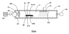
図2A及び図2Bに示すように、コーティング機器は、新規のプラズマ体重合コーティング方法を実行するように配置され、基材90の表面91にポリマーフィルム層92を形成し、本発明による第1好適な実施例に記載されるものである。より具体的に、前記コーティング機器は、反応チャンバ11を規定したチャンバ体10と、前記反応チャンバ11に連通しており、ガスモノマー又はモノマー蒸気であるフィルム層形成材料201を前記チャンバ体10の前記反応チャンバ11に導入するためのモノマー放出ソース20と、前記反応チャンバ11の内部において誘導電界を生成し、プラズマ体を形成するように操作されるプラズマ励起ソース30とを含み、前記プラズマ励起ソース30が前記フィルム層形成材料201に電気エネルギーを印加し、前記フィルム層形成材料201を励起するように、前記フィルム層形成材料201を分解させ、活性前駆体を形成し、これによって、前記フィルム層形成材料201は、プラズマ体状態に活性化され、活性前駆体とモノマーとの間の反応、及び前記チャンバ体10の前記反応チャンバ11における活性前駆体の間の反応を誘発し、前記基材90の前記表面91に前記ポリマーフィルム層92を堆積して形成する。
As shown in FIGS. 2A and 2B, coating equipment is arranged to carry out the novel plasma polymerization coating method to form a
本発明の当該好適な実施例によれば、図2Bに示すように、前記プラズマ励起ソース30は、前記チャンバ体10の前記反応チャンバ11において前記モノマー放出ソース20から離れた位置に配置される。前記チャンバ体10は前記モノマー放出ソース20とプラズマ励起ソース30との間に配置される基材位置決め領域12を有し、これによって、少なくとも1つの前記基材90は前記モノマー放出ソース20と前記プラズマ励起ソース30との間の前記反応チャンバ11に配置され、本発明のプラズマ体重合コーティング方法で、前記基材90の前記表面91の前記ポリマーフィルム層92を形成するために用いられる。
According to the preferred embodiment of the present invention, the
相応的に、前記基材90のプラズマ体重合コーティング方法で、1つ又は複数の前記基材90は、前記モノマー放出ソース20が前記チャンバ体10の前記基材位置決め領域12の第1側に配置され、前記プラズマ励起ソース30が前記基材90の相対する第2側に位置するように、基材主体11の前記基材位置決め領域12に設けられることで、前記フィルム層形成材料201が前記チャンバ体10の前記反応チャンバ11に放出される場合、前記フィルム層形成材料201は前記基材90に達する前、前記プラズマ励起ソース30を通過する必要がなくなり、前記フィルム層形成材料201の過度分解を避ける。
Correspondingly, in the plasma polymerization coating method of the
具体的に、前記モノマー放出ソース20が前記フィルム層形成材料201を放出するように操作される場合、前記フィルム層形成材料201は前記チャンバ体10の前記反応チャンバ11に分散し、まず、チャンバ体10の前記基材位置決め領域12に達し、一部の前記フィルム層形成材料201のみが前記プラズマ励起ソース30により励起され、前記フィルム層形成材料201を分解して重合させ、基材の前記表面91に堆積させ、前記ポリマーフィルム層92を形成する。
Specifically, when the
本発明のプラズマ体重合コーティング方法で、前記基材90は、前記モノマー放出ソース20から前記プラズマ励起ソース30へ流れる前記フィルム層形成材料201の流動経路に配置され、前記基材90と前記モノマー放出ソース20との距離は、前記基材90と前記プラズマ励起ソース30との間の距離より小さく、全ての前記フィルム層形成材料201はいずれも前記プラズマ励起ソース30により励起されていないため、前記フィルム層形成材料201の過度分解を避ける。
In the plasma polymerization coating method of the present invention, the
前記基材90は直接的に前記チャンバ体10の前記基材位置決め領域12に配置されてもよい。又は、図2Bに示すように、複数の前記基材90は前記支持フレーム40に配置され、複数の前記基材90が積載された前記支持フレーム40は、前記チャンバ体10の前記基材位置決め領域12に配置されるとともに、前記チャンバ体10の前記反応チャンバ11に収容される。又は、前記支持フレーム40は前記チャンバ体10の前記基材位置決め領域12に配置されるとともに、前記チャンバ体10の前記反応チャンバ11に収容され、複数の前記基材90は前記支持フレーム40に配置される。別の実施可能な形態において、前記支持フレーム40は前記チャンバ体10に装着されるとともに、前記反応チャンバ11に配置され、コーティングプロセスで、複数の前記基材90は前記支持フレーム40に配置される。
The
前記支持フレーム40は、多層の前記基材90を支持するための複数の支持プラットフォームを有する担持スタンド41を含む。前記担持スタンド41は前記基材90を配置して支持するための支持領域411を有し、前記支持領域411は前記モノマー放出ソース20と前記プラズマ励起ソース30との間に配置される。実施可能な形態において、前記支持フレーム40全体は前記モノマー放出ソース20と前記プラズマ励起ソース30との間に配置されるわけではなく、前記基材90を支持するための前記支持フレーム40の前記支持領域411は、前記モノマー放出ソース20と前記プラズマ励起ソース30との間に配置され、前記支持フレームの前記支持領域411に配置される前記基材90は、前記モノマー放出ソース20と前記プラズマ励起ソース30との間に配置されてもよい。
The
当業者が理解すべきなのは、前記チャンバ体10の前記基材位置決め領域12は1つ又は複数の前記基材90を直接的に支持するための領域、或いは1つ又は複数の前記基材90が積載される前記支持フレーム40を支持して収容するための領域である。
Those skilled in the art should understand that the
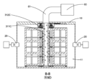
本発明のチャンバ体10は前記反応チャンバ11を限定するハウジングである。前記チャンバ体10の前記反応チャンバ11の横断面は、円、楕円形、多角形、例えば矩形、五角形、六角形、七角形、八角形、九角形、及び十角形であってもよいが、これらに限定されていない。当該好適な実施例の1つの実施例として、前記チャンバ体10は、矩形の反応チャンバ11を有するように構造される。前記モノマー放出ソース20は矩形の前記反応チャンバ11の第1側に配置され、前記プラズマ励起ソース30は矩形の前記反応チャンバ11の相対する第2側に配置される。図面に示すように、前記プラズマ励起ソース30が前記モノマー放出ソース20から離間すると同時に、前記モノマー放出ソース20は前記チャンバ体10の前記第1側壁101に隣接するように配置され、前記プラズマ励起ソース30は前記チャンバ体10の前記第2側壁102に配置され、前記第2側壁102と前記チャンバ体10の前記第1側壁101とは対向する。
The
前記モノマー放出ソース20は、前記フィルム層形成材料201を前記チャンバ体10の前記反応チャンバ11に導入するための少なくとも1つの放出入口21を有する。前記放出入口21は前記チャンバ体10の壁に形成され、前記チャンバ体10の壁層を突き通す。任意に選べることとして、前記放出入口21は供給ノズルに形成され、前記チャンバ体10に嵌め込まれる。任意に選べることとして、前記放出入口21は供給ノズルに形成され、1つの原料供給ヘッドは原料供給管の遠位に位置し、前記チャンバ体10の前記反応チャンバ11に延在する。
The
本発明の当該好適な実施例によれば、前記コーティング装置は、前記フィルム層形成材料201を前記モノマー放出ソース20に供給するためのモノマー供給ユニット50をさらに含む。より具体的に、当該好適な実施例の前記モノマー供給ユニット50は、前記フィルム層形成材料201の原材料202を貯蔵するための材料貯蔵器51と、原材料202を気化するための気化器52と、前記原材料202を前記材料貯蔵器51から前記モノマー放出ソース20に搬送するための搬送管システム53と、を含む。相応的に、前記モノマー放出ソース20によって放出される前記フィルム層形成材料201は、気化されたモノマー材料である。前記フィルム層形成材料201の前記原料202は単一又は混合された液体、或いは液体/固体スラリーであってもよく、前記気化器52は、霧化装置、加熱装置、及び超音波ノズル又は噴霧器を含んでもよい。例えば、前記気化器52は、前記原料202を前記搬送管システム53に加熱し、気化モノマー材料を生成するように提供される加熱装置を含む。前記加熱装置は前記搬送管システム53の任意位置で提供されてもよい。具体的に、前記加熱装置は、液体前記原料202が前記モノマー放出ソース20に搬送された場合、前記原料202が前記加熱装置により加熱され、前記反応チャンバ11に放出される気化モノマー材料を生成するように、前記モノマー放出ソース20に対応する位置に提供される。
According to the preferred embodiment of the present invention, the coating apparatus further includes a
前記フィルム層形成材料201の前記原料202は粉末であってもよく、前記気化器52はフラットスプレ一ガス噴射気化器であってもよい。また、前記フィルム層形成材料201とともに、キャリアガスを供給してもよい。前記材料貯蔵器51、前記気化器52、前記搬送管システム53及び前記モノマー放出ソース20の数は限定されず、いくつかの実施例において、1つ又は複数の前記材料貯蔵器51、前記気化器52、前記搬送管システム53及び前記モノマー放出ソース20を採用してもよい。
The
前記プラズマ励起ソース30の放電方式は、直流放電、交流放電、オーディオ放電、容量結合又は誘導結合による無線周波放電、共振キャビティマイクロ波放電、表面波結合或いは電子サイクロトロン共鳴、中間周波放電、ペニング放電、火花放電及びパルス放電を含むが、これらに限定されていない。また、前記プラズマ励起ソース30は連続的又はパルス方式で放電するように操作される。
The discharge method of the
図2A及び図2Bに示すように、前記プラズマ励起ソース30は、前記チャンバ体10の前記反応チャンバ11にプラズマ体を生成するように、前記反応チャンバ11に電界を生成するための電極装置31を含む。当該好適な実施例において、前記電極装置31は第1電極311と第2電極312とを含み、第1電極311と第2電極312との間には放出場313が画成される。例示として、当該好適な実施例の1対の電極311、312は正負電極として、前記チャンバ体10の前記反応チャンバ11において前記モノマー放出ソース20から離れた位置に設けられるとともに、チャンバの外側に配置される、例えばRF発生器のようなエネルギー源に接続される。任意に選べることとして、前記第1電極311は前記エネルギー源に電気接続され、前記第2電極312は接地できる。好ましくは、各前記第1電極311及び第2電極312は、前記反応チャンバ11内の前記放出場313に連通する複数の孔を有する多孔質電極として実施されてもよい。
As shown in FIGS. 2A and 2B, the
前記フィルム層形成材料201自体は、プラズマ体ソースガスとして機能してもよい。また、前記コーティング機器はプラズマ体ソースガス供給ユニットをさらに含み、不活性ガス及び窒素を含むが、これらに限定されていないプラズマ体ソースガスを、前記チャンバ体10の前記反応チャンバ11に供給する。前記モノマー放出ソース20は前記フィルム層形成材料201を前記反応チャンバ11に供給する前、前記プラズマ励起ソース30の作用で、プラズマ体ソースガスを前記反応チャンバ11に注入し、プラズマ体を生成することで、プラズマ体環境を提供する。また、キャリアガスをプラズマ体ソースガスとし、前記フィルム層形成材料201を前記反応チャンバ11に供給する前、キャリアガスを前記反応チャンバ11に導入し、プラズマ体を生成する。
The film
特筆に値するのは、当業者が理解できるように、フィルム層形成材料201を放出するための1つ又は複数の別途の放出ソースは、前記プラズマ励起ソース30が前記基材90と前記フィルム層形成材料201を放出するための付加的な放出ソースとの間に位置するように、チャンバ体10に配置される。これらの実施例において、一部の前記フィルム層形成材料201は、前記チャンバ体の基材位置決め領域12に隣り合う位置で、前記モノマー放出ソース20から放出される。他の一部の前記フィルム層形成材料201は付加的な放出ソースから放出され、前記基材90に達する前、前記プラズマ励起ソース30を通過し、これによって、全ての前記フィルム層形成材料201がいずれも前記プラズマ励起ソース30により励起されるわけではなく、全ての前記フィルム層形成材料201を小さい物質に分解することを防止する。
Notably, as one skilled in the art will appreciate, one or more separate emitting sources for emitting film
また、前記コーティング機器は他の部材、例えば、前記プラズマ励起ソース30に隣接するとともに、前記モノマー放出ソース20から離れており、前記チャンバ体10の前記反応チャンバ11内の圧力を調節するための圧力調節ユニット60と、前記コーティング機器の操作を制御するための制御ユニットと、排気ガスを収集するための排気ガス管と、を含んでもよい。本発明のプラズマ体重合コーティング方法で、前記フィルム層形成材料201を前記反応チャンバ11に供給する前、圧力調節ユニット60の作用で、前記反応チャンバ11は真空室になる。用語「真空室」は、チャンバがチャンバの外部より、低い空気圧を有することを指し、前記用語は必ずしも、チャンバが真空状態に排気されることを意味するとは限らない。
The coating equipment also includes other components, for example, adjacent to the
本発明の前記基材90は金属、ガラス、セラミック、ポリマー、織物、繊維、粉末、及び半導体を含み、電子素子又は電子機器、機械部材或いは機械機器、編み物であってもよいが、これらに限定されず、例えば、電子部材又は電子機器は、携帯電話、ポケットベル、ラジオ、スピーカー、マイク、リンガー、ブザー、補聴器、オーディオプレイヤー、テレビ、ノートブック、ノートブック、タブレット、キーボード、PCB基板、ディスプレイ又はセンサーであってもよいが、これらに限定されていない。前記ポリマーフィルム層92は疎水性コート層、親水性コート層、疎油性コート層、防錆コート層、防カビコート層、防湿コート層、電気/熱伝導性コート層、生物医学コート層、光学コート層及び摩擦コート層であってもよいが、これらに限定されていない。前記ポリマーフィルム層92は前記基材90の前記表面91に堆積し、前記基材90の表面全体、又は前記基材90の表面全体の一部の領域であってもよい。
The
前記ポリマーフィルム層92はアクリル酸コート層、エポキシコート層、有機シリコーンコート層、ポリウレタンコート層又はパラキシレンコート層であってもよく、典型的な前記ポリマーフィルム層92は疎水性ポリマーコート層であり、前記フィルム層形成材料201はCF3ベースの過フッ素化化合物、パーフルオロオレフィン、水素含有不飽和化合物、任意選択で置換されたアルキン、ポリエーテル置換オレフィン、2つの二重結合を含む有機化合物、少なくとも5つの炭素原子の任意選択で置換されたアルキル鎖(任意に選べることとして、ヘテロ原子が挿入された)を有する飽和有機化合物、少なくとも1つのヘテロ原子を含む大環状化合物を含む。
The
前記フィルム層形成材料201は単一分子のモノマー、オリゴマー又はその組成物などであってもよく、例えば、オリゴマーはダブルポリマー、例えば、Parylene C、Parylene Nなどである。前記フィルム層形成材料201の実施例として、モノマーは一種又は複数種の単官能性不飽和フルオロ化合物と一種又は複数種の多官能性不飽和炭化水素誘導体との混合物である。フルオロ化合物はメタクリル3-(パーフルオロ-5-メチルヘキシル)-2-ヒドロキシプロピルエステル、メタクリル2-(パーフルオロデシル)エチルエステル、メタクリル2-(パーフルオロヘキシル)エチルエステル、1,1,2,2-アクリル酸テトラヒドロパーフルオロテトラデシルエステル、アクリル酸1H、1H、2H、2H-ヘプタデカフルオロデシル、アクリル酸1H、1H、2H、2H-パーフルオロオクチル、アクリル酸2-(パーフルオロブチル)エチル、(2H-パーフルオロプロピル)-2-アクリレート、(パーフルオロシクロヘキシル)アクリル酸メチル、3、3、3-トリフルオロ-1-プロピン、1-エチニル基-3、5-ジフルオロベンゼン及び4-エチニル基-トリフルオロトルエンを含むが、これらに限定されていない。前記多官能性不飽和炭化水素誘導体は、エトキシル化トリメチロールプロパントリアクリレート、トリプロピレングリコールジアクリレート、ジビニルベンゼン、ポリ(エチレングリコール)アクリレート、1、6-ヘキシレングリコールジアクリレート、エチレングリコールジアクリレート、ジエチレングリコールジビニルエーテル及びネオペンチルグリコールジアクリラートを含むが、これらに限定されていない。
The film
別の例示として、前記表面91を化学腐食から保護し、疎水性能を強めるために、前記ポリマーフィルム層92は前記基材90の前記表面91に形成される。より具体的に、モノマーは以下の式で示される構成を有する。
As another example, the
ただし、R1、R2及びR3は疎水基であり、個別に水素、アルキル、ハロゲン、又はハロアルキルから選択され、mは0~8の整数であり、nは1~15の整数であり、XはH又はハロゲン、さらに、ハロゲンFである。 However, R1, R2 and R3 are hydrophobic groups and are individually selected from hydrogen, alkyl, halogen, or haloalkyl, m is an integer of 0 to 8, n is an integer of 1 to 15, and X is H or halogen, furthermore halogen F.
図2Cに示すように、上記第1好適な実施例による前記コーティング機器の実施可能な形態を記載する。前記支持フレーム40は前記室体10の前記反応チャンバ11に移動可能に設けられる。具体的な実施例において、前記支持フレーム40はその中心軸周りに回転するように操作されることで、前記基材90の、前記反応チャンバ11での位置を調節でき、これによって、前記基材90と前記プラズマ励起ソース30との間の距離を調節し、さらに、前記基材90と前記モノマー放出ソース20との間の距離を調節し、前記基材90の前記表面91に堆積形成されるポリマー材料の構成を制御及び調節する。
As shown in FIG. 2C, a possible embodiment of the coating device according to the first preferred embodiment is described. The
上記第1好適な実施例によれば、図2Dに示すように、前記コーティング装置の別の実施可能な形態である。前記実施形態において、前記モノマー供給ユニット50は気化器を必要せず、前記フィルム層形成材料201のガス原料を貯蔵するための材料貯蔵装置51を含む。言い換えると、前記フィルム層形成材料201は前記材料貯蔵装置51に貯蔵され、前記搬送管システム53によって直接的に前記モノマー放出ソース20に送られる。
According to the first preferred embodiment, another possible embodiment of the coating apparatus is shown in FIG. 2D. In the embodiment, the
例えば、当該好適な実施例の前記コーティング機器は、前記基材90の前記表面91にDLC(ダイヤモンドライクカーボン)膜を形成する。主にガス状炭化水素からなる前記フィルム層形成材料201を直接的に前記コーティング機器の前記反応チャンバ11に導入することで、PECVDプロセスを実施する。
For example, the coating device of the preferred embodiment forms a DLC (diamond-like carbon) film on the
相応的に、本発明は、前記コーティング装置が前記基材90でコーティングを行うためのコーティング方法を提供し、前記コーティング方法は、
(a)前記基材90を、前記チャンバ体10の前記反応チャンバ11における前記モノマー放出ソース20と前記プラズマ励起ソース30との間の位置に配置するステップと、
(b)前記モノマー放出ソース20によって、前記フィルム層形成材料201を前記反応チャンバ11に導入し、PECVDプロセスを実施することで、前記プラズマ励起ソース30の作用で、前記基材90の前記表面91に前記ポリマーフィルム層92を形成するステップと、を含む。
Correspondingly, the present invention provides a coating method for the coating device to perform coating on the
(a) arranging the
(b) introducing the film
ステップ(a)は、1つ又は複数の前記基材90をチャンバ体の前記基材位置決め領域12に配置するステップを含み、前記モノマー放出ソース20及び前記プラズマ励起ソース30がそれぞれ1つ又は複数の前記基材90の両側に設けられる。
Step (a) includes positioning one or more of the
好ましくは、ステップ(a)は、1つ又は複数の前記基材90を前記支持フレーム40に配置し、前記支持フレーム40及び前記基材90をともに、チャンバ体の前記基材位置決め領域12に配置するステップを含み、前記モノマー放出ソース20及び前記プラズマ励起ソース30がそれぞれ前記支持フレーム40の両側に設けられる。
Preferably, step (a) includes arranging one or more of the
任意に選べることとして、ステップ(a)は、前記反応チャンバ11における前記チャンバ体10の前記基材位置決め領域12に前記支持フレーム40を構成し、前記支持フレーム40に1つ又は複数の前記基材90を積載するステップを含み、前記支持フレーム40は前記チャンバ体10に装着又は固定され、或いは単に前記反応チャンバ11に配置される。
Optionally, step (a) comprises configuring the
特筆に値するのは、1つ又は複数の前記基材90は水平、傾斜又は垂直に前記チャンバ体10の前記反応チャンバ11に配置される。
Notably, one or more of the
ステップ(a)において、前記コーティング方法は、間隔をあけて前記反応チャンバ11に前記モノマー放出ソース20及び前記プラズマ励起ソース30を配置し、前記チャンバ体10の前記反応チャンバ11の2つの対向側では、前記フィルム層形成材料201が前記モノマー放出ソース20からプラズマ励起ソース30へ流れる流動経路に、少なくとも一部の前記フィルム層形成材料201が、前記プラズマ励起ソース30に達する前、基材を配置した前記基材位置決め領域12を通過する必要があるように、1つ又は複数の前記基材90を配置するステップを含む。
In step (a), the coating method includes arranging the
ステップ(b)は、前記原料202を気化することで、気化モノマーとしての前記フィルム層形成材料201を形成し、前記フィルム層形成材料201を前記モノマー放出ソース20に搬送し、これによって、前記フィルム層形成材料201を前記チャンバ体10の前記反応チャンバ11に供給するステップを含む。相応的に、前記フィルム層形成材料201はポンプによって、前記反応チャンバ11に注入され、又は前記反応チャンバ11の圧力の低下のため、前記反応チャンバ11に吸入される。
In step (b), the
ステップ(b)は、ガスモノマーとしての前記フィルム層形成材料201を前記モノマー放出ソース20に供給することで、前記フィルム層形成材料201を前記チャンバ体10の前記反応チャンバ11に供給するステップを含む。
Step (b) comprises supplying the film
当該好適な実施例によれば、ステップ(b)において、図2Bに示すように、前記フィルム層形成材料201は前記モノマー放出ソース20によって、前記プラズマ励起ソース30に向いて前記チャンバ体10に散布する。例えば、前記プラズマ励起ソース30に向いて、前記フィルム層形成材料201を水平に前記チャンバ体10に注入するが、前記支持フレーム40は前記モノマー放出ソース20と前記プラズマ励起ソース30との間に配置され、前記フィルム層形成材料201は、前記基材90に対してプラズマ体処理を行うための前記基材90に達する前、前記プラズマ励起ソース30を通過する必要がなくなるため、全ての前記フィルム層形成材料201はいずれも前記プラズマ励起ソース30により活性化されて励起されるわけではない。
According to the preferred embodiment, in step (b), the film
図3A~図3Cに示すように、本発明の第2好適な実施例による前記コーティング機器を記載する。当該好適な実施例の前記コーティング機器は、反応チャンバ11を有するチャンバ体10と、ガスフィルム層形成材料201を前記チャンバ体10の前記反応チャンバ11に放出するためのモノマー放出ソース20と、前記反応チャンバ11から離れたプラズマ励起ソース30とを含む。前記プラズマ励起ソース30は、前記フィルム層形成材料201を活性化して励起し、且つ支持領域411Aに基材90の支持フレーム40Aを支持及び担持するように操作されることで、前記プラズマ励起ソース30は操作され、前記フィルム層形成材料201は前記反応チャンバ11に注入された場合、前記ポリマーフィルム層92が前記基材90の前記表面91に堆積して形成されることを許可するように、前記基材90は前記プラズマ励起ソース30から生成したプラズマ体に曝される。
As shown in FIGS. 3A to 3C, the coating equipment according to a second preferred embodiment of the present invention is described. The coating equipment of the preferred embodiment comprises a
当該好適な実施例において、前記支持フレーム40Aは、前記チャンバ体10の前記反応チャンバ11内で移動可能な支持部材として実施される。特に、前記支持フレーム40Aは前記モノマー放出ソース20と前記プラズマ励起ソース30との間を移動できる。前記支持フレーム40の運動方式は、線形運動、曲線運動、摺動運動又は回転運動であってもよいが、これらに限定されず、これによって、前記反応チャンバ11内の前記基材90の位置を調整し、前記基材90に堆積されるモノマー、及び分解される前駆体の量を調節し、前記基材90の前記表面91に形成される前記ポリマーフィルム層92の品質を向上させる。いくつかの実施例において、前記支持フレーム40Aの移動は、基本的に同様なプラズマ体重合環境を複数の前記基材90に提供し、前記基材90に形成される前記ポリマーフィルム層92の均一性を向上させる。
In the preferred embodiment, the
前記支持フレーム40Aの移動は、前記基材90と前記モノマー放出ソース20との間に相対変位を発生させ、又は前記基材90と前記プラズマ励起ソース30との間に相対変位を発生させ、或いは上記2つの等価状態を発生させるように構造され、前記基材90に達した、前記プラズマ励起ソース30により励起されていないモノマーの量、或いはモノマーを分解させることによって、生成した活性前駆体の量を調節でき、前駆体と活性前駆体との十分な反応を確保する。
Movement of the
特筆に値するのは、前記支持フレーム40Aの運動は制御ユニットにより制御され、前記制御ユニットは移動、移動時間間隔又は移動速度を調整するようにプログラムされ、これによって、前記基材90に所望のプラズマ体重合環境を提供し、前記ポリマーフィルム層92の分子構成から、必要な分岐及び架橋を取得し、高品質を有するポリマーフィルム層92を形成する。
Notably, the movement of the
当該好適な実施例によれば、図3A~図3Cに示すように、前記支持フレーム40Aは移動可能な支持部材として実現され、移動可能な前記支持部材は前記モノマー放出ソース20と前記プラズマ励起ソース30との間で繰り返し移動できることで、前記基材90と前記モノマー放出ソース20との間の距離、及び前記基材90と前記プラズマ励起ソース30との間の距離を調節する。
According to the preferred embodiment, as shown in FIGS. 3A to 3C, the
具体的な実施例において、前記チャンバ体10は矩形の前記反応チャンバ11を有し、前記モノマー放出ソース20と前記プラズマ励起ソース30とは前記チャンバ体10の同一側壁に配置され、間隔をあけて互いに離間される。例えば、前記モノマー放出ソース20と前記プラズマ励起ソース30とは前記チャンバ体10の頂側壁103に配置される。プラズマ体重合コーティング方法で、前記モノマー放出ソース20は前記フィルム層形成材料201を放出し、モノマー領域は前記モノマー放出ソース20の前面に規定され、運転過程で、前記プラズマ励起ソース30はその周囲にプラズマ体発生領域を形成し、前記支持フレーム40Aはモノマー領域とプラズマ体領域との間で往復移動する。
In a specific embodiment, the
図面に示すように、当該好適な実施例において、前記フィルム層形成材料201は前記モノマー放出ソース20によって前記プラズマ励起ソース30に向いて、前記反応チャンバ11に分散していなく、横方向に前記反応チャンバ11に導入されてから、縦方向に沿って前記基材90及び前記プラズマ励起ソース30に分散し、これによって、前記モノマー放出ソース20から放出した前記フィルム層形成材料201の気流は、直接的に前記プラズマ励起ソース30の周囲に生成したプラズマ体に吹き付けることなく、モノマーから分解された反応前駆体物質及びモノマーは理想な混合性能を具備する。
As shown in the drawings, in the preferred embodiment, the film layer-forming
当業者が理解すべきなのは、前記支持フレーム40Aは、前記モノマー放出ソース20と前記プラズマ励起ソース30との間を移動するように操作され、電動モータ、空気圧駆動システム、又は油圧駆動システムを利用してもよい。前記チャンバ体10には、前記支持フレーム40Aを適切な位置に保持し、且つ前記支持フレーム40Aの運動を案内して限定するためのガイドレール又は案内溝が設けられる。
Those skilled in the art should understand that the
図面に示すように、当該好適な実施例の前記プラズマ励起ソース30の前記電極装置31は、前記反応チャンバ11に延在する平面電極、又は電界を発生させる他の電極装置として構造されてもよい。
As shown in the drawings, the
相応的に、本発明の当該好適な実施例は、前記ポリマーフィルム層92を前記基材90の前記表面91に堆積させるためのコーティング方法を提供し、前記コーティング方法は、
(A)前記プラズマ励起ソース30から離れた前記モノマー放出ソース20によって、前記フィルム層形成材料201を前記チャンバ体10の前記反応チャンバ11に供給するステップと、
(B)前記モノマー放出ソース20と前記プラズマ励起ソース30との間で前記基材90を移動させるステップと、
(C)前記プラズマ励起ソース30を活性化し、前記基材90に対してプラズマ体処理を行うことで、前記基材90の前記表面91に前記ポリマーフィルム層92を形成するステップと、を含む。
Correspondingly, the preferred embodiment of the invention provides a coating method for depositing the
(A) supplying the film
(B) moving the
(C) forming the
ここで、上記ステップ(A)、(B)及び(C)のステップの順序は限定されていない。ステップ(B)において、前記ステップは、前記基材90を前記支持フレーム40Aに担持し、前記支持フレーム40Aを前記モノマー放出ソース20と前記プラズマ励起ソース30との間を繰り返して往復移動させるように駆動するステップを含む。好適な例示として、前記支持フレーム40Aを移動させるように駆動することで、前記基材90と前記モノマー放出ソース20との間の距離、及び前記基材90と前記プラズマ励起ソース30との間の距離を調節する。
Here, the order of steps (A), (B), and (C) above is not limited. In step (B), the step includes supporting the
図4Aに示すように、別の実施可能な形態において、前記モノマー放出ソース20及び前記プラズマ励起ソース30は、前記チャンバ体10の2つの対向する側壁に隣り合うように配置される。例えば、前記モノマー放出ソース20は頂側壁103に隣接するように配置され、前記プラズマ励起ソース30は前記チャンバ体10の底側壁104に装着される。図4Bに示すように、別の実施可能な形態として、前記基材90に前記フィルム層形成材料201を放出するように、前記モノマー放出ソース20は前記チャンバ体10の端側壁101に隣り合うように配置され、前記プラズマ励起ソース30は前記チャンバ体10の底壁104に配置される。言い換えると、前記モノマー放出ソース20及び前記プラズマ励起ソース30は前記チャンバ体10の隣接側壁101、104に配置される。
As shown in FIG. 4A, in another possible embodiment, the
図5A及び図5Bに示すように、上記好適な実施例において、前記プラズマ励起ソース30は前記支持フレーム40Aの側面に装着され、別の実施可能な形態として、前記モノマー放出ソース20に対向する。前記支持フレーム40Aは移動不可であり、又は好ましくは、前記支持フレーム40Aは移動可能に配置されることで、前記支持フレーム40Aと前記モノマー放出ソース20との間の距離、及び前記モノマー放出ソース20と前記プラズマ励起ソース30との間の距離を調節する。当該好適な実施例によれば、前記基材90と前記プラズマ励起ソース30との間の相対位置を固定できるが、前記プラズマ励起ソース30は前記支持フレーム40Aとともに移動でき、プラズマ体の、前記チャンバ体10の前記反応チャンバ11内でのプラズマ体生成環境を変更する。
As shown in FIGS. 5A and 5B, in the preferred embodiment, the
図6A及び図6Bに示すように、前記コーティング装置の別の実施可能な形態を示す。前記実施例において、当業者が理解すべきなのは、前記支持フレーム40Aは、前記プラズマ励起ソース30が前記モノマー放出ソース20と前記基材90との間に位置するように、ある位置に移動してもよい。ところが、前記支持フレーム40Aが前記モノマー放出ソース20と前記プラズマ励起ソース30との間を移動する過程で、全てのフィルム層形成材料201が前記基材90に達する前、前記プラズマ励起ソース30を通過するわけではないように、前記フィルム層形成材料201は前記プラズマ励起ソース30に達する前、前記支持フレーム40Aを通過する必要がある。
As shown in FIGS. 6A and 6B, another possible embodiment of the coating apparatus is shown. In the embodiment, those skilled in the art should understand that the
言い換えると、当該好適な実施例は、前記ポリマーフィルム層92を前記基材90の前記表面91に堆積させるためのコーティング方法を提供し、当該方法は以下のステップを含む。
In other words, the preferred embodiment provides a coating method for depositing the
前記チャンバ体10の前記反応チャンバ11で前記基材90を移動させる。これによって、前記基材90の移動経路を限定し、少なくとも一部の移動経路期間において、前記基材90は前記モノマー放出ソース20と前記プラズマ励起ソース30との間に位置する。
The
前記フィルム層形成材料201を前記チャンバ体10の反応チャンバに放出する。これによって、前記プラズマ励起ソース30の操作期間において、前記基材90に対するプラズマ体処理を活性化する。
The film
相応的に、前記基材90の移動経路を第1部分及び第2部分に区画し、第1部分において前記モノマー放出ソース20及び前記プラズマ励起ソース30はそれぞれ前記基材90の両側にあり、第2部分において前記モノマー放出ソース20及び前記基材90はそれぞれ前記プラズマ励起ソース30の両側にあり、前記支持フレーム40Aにより担持される前記基材90の移動経路の第1部分は明らかに第2部分より大きい。
Correspondingly, the movement path of the
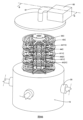
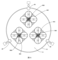
図7は本発明の第3好適な実施例によるコーティング装置を示す。より具体的に、当該好適な実施例の前記コーティング機器は、反応チャンバ11を有するチャンバ体10と、ガスフィルム層形成材料201を前記チャンバ体10の前記反応チャンバ11に放出するための1つ又は複数のモノマー放出ソース20と、前記フィルム層形成材料201を励起するためのプラズマ励起ソース30と、前記基材90を支持して搬送するための支持フレーム40Bであって、前記プラズマ励起ソース30Bが操作され、且つ前記フィルム層形成材料201が1つ又は複数の前記モノマー放出ソース20によって前記反応チャンバ11に送られた場合、前記基材90の前記表面91に前記ポリマーフィルム層92を堆積して形成する支持フレーム40Bと、を含む。
FIG. 7 shows a coating apparatus according to a third preferred embodiment of the invention. More specifically, the coating equipment of the preferred embodiment comprises a
当該好適な実施例によれば、前記プラズマ励起ソース30Bは前記支持フレーム40Bの略中央領域に配置される。好ましくは、前記プラズマ励起ソース30Bは前記チャンバ体10の前記反応チャンバ11の中心に配置されてもよく、前記ポリマーフィルム層92が堆積される複数の前記基材90は、前記プラズマ励起ソース30Bの周囲に配置される。前記基材90は前記プラズマ励起ソース30Bを取り囲むことで、前記プラズマ励起ソース30Bと前記モノマー放出ソース20との間に配置される。
According to the preferred embodiment, the
具体的に、複数、例えば、4つの前記モノマー放出ソース20は、前記チャンバ体10の内壁に隣り合う位置に配置され、前記フィルム層形成材料201は前記チャンバ体10の内部周辺の隣接位置に放出され、前記チャンバ体10の中心位置にある前記プラズマ励起ソース30Bに流れる。複数の前記モノマー放出ソース20及び前記プラズマ励起ソース30Bは前記基材90の2つの対向する側に設けられるため、前記フィルム層形成材料201の過度分解を防止する。
Specifically, a plurality of, for example, four,
本発明の当該好適な実施例の前記プラズマ励起ソース30Bは、電力を前記チャンバ体10内に放出された前記フィルム層形成材料201に印加するための電極装置31Bを含む。より具体的に、1つの実施例として、前記電極装置31Bは少なくとも1対の電極を含み、好ましくは、複数対の第1電極311B及び第2電極312Bは前記反応チャンバ11の中央に設けられる。図7に示すように、各前記第1電極311B及び前記第2電極312Bはそれぞれ前記チャンバ体10の前記反応チャンバ11に垂直に配置される細長い電極板として実施される。前記例示的な実施例において、4つの前記第1電極311B及び4つの前記第2電極312Bは円周方向に沿って交互に配置される。
The
前記第1電極311B、前記第2電極311Bは正電極及び負電極であり、それぞれ前記チャンバ体10の外側にある、RF発生器のようなエネルギー源の2つの接続端に電気接続される。任意に選べることとして、前記第1電極311Bはエネルギー源に電気接続され、第2電極312Bは接地できる。
The
本実施形態の前記支持フレーム40Bは、1つ又は複数の前記基材90を搬送するための1つ又は複数の担持スタンド41Bを含む。各前記担持スタンド41Bは前記基材90を位置決めるための支持領域411Bを有し、前記基材90は水平方向、傾斜、及び垂直で、支持領域411Bに配置されてもよい。本実施例において、前記基材90は前記支持領域411Bに水平配置されるとともに、前記支持領域411Bに保持され支持される。
The
当該好適な実施例において、1つ又は複数の担持スタンド41Bの複数の前記支持領域411Bは前記プラズマ励起ソース30Bと前記モノマー放出ソース20との間に設けられることで、1つ又は複数の前記基材90が相応する前記支持領域411Bに配置される場合、前記モノマー放出ソース20及び前記プラズマ励起ソース30Bはそれぞれ対応する前記基材90の2つの対向側に配置される。
In the preferred embodiment, the plurality of
また、当該好適な実施例の前記支持フレーム40Bの各前記担持スタンド41Bは複数の前記基材90を搬送し、前記反応チャンバ11を移動でき、各前記担持スタンド41Bの運動方式は線形運動、曲線運動、摺動運動及び回転運動であってもよいが、これらに限定されていない。当該好適な実施例の具体的な例示として、前記支持フレーム40Bの各前記担持スタンド41Bはその中心軸線Y周りに回転するように操作される。
In addition, each of the supporting stands 41B of the supporting
本実施形態の前記支持フレーム40Bは、1つ又は複数の担持スタンド41Bを支持するための可動スタンド42Bをさらに含む。前記可動スタンド42Bの移動も線形運動、曲線運動、摺動運動及び回転運動であってもよいが、これらに限定されていない。
The
当該好適な実施例によれば、前記可動スタンド42Bは回転台として、円形室の反応チャンバにおいて中心軸線X周りに回転するように実施され、担持スタンド41Bは可動スタンド42Bに支持されるため、各前記担持スタンドは可動スタンド42Bに連れて移動するとともに、その中心軸線Yに対して自転し、このように、前記担持スタンド41Bの2つの移動は、各前記基材90と前記プラズマ励起ソース30との間の相対位置を変更する。
According to the preferred embodiment, the
図8A~図8Eに示すように、本発明の上記第3好適な実施例の可能な形態として、前記コーティング機器はプラズマ励起ソース30Cと、電極装置31Cとを含む。当該好適な実施例の前記電極装置31Cは第1電極311Cと第2電極312Cとを含み、各電極はいずれも円柱状電極として実施され、前記第1電極311Cは前記第2電極312Cの周囲に外嵌されることで、前記第1電極311Cと前記第2電極312Cとの間に円形放出場313Cを規定する。前記第1電極311Cは、例えばRF発生器のようなエネルギー源に電気接続され、前記第2電極312Cは接地できる。
As shown in FIGS. 8A-8E, as a possible form of the third preferred embodiment of the present invention, the coating equipment includes a
また、前記第1電極311Cは、前記反応チャンバ11内の前記放出場313Cに連通する複数の孔を有する多孔質電極として実施される。前記第2電極312Cは前記反応チャンバ11に連通する連通孔を有する細長い管として形成されることで、前記第2電極312Cは前記チャンバ体の前記反応チャンバ11の外側に連通する抽気管として、前記チャンバ体10の前記反応チャンバ11からガス混合物を抽出し、前記反応チャンバ11内の圧力を調節し、前記反応チャンバ11における排気ガスを除去する。
Further, the
図8B~図8Eに示すように、当該好適な実施例の前記コーティング機器は、反応チャンバ11を有するチャンバ体10と、ガスフィルム層形成材料201を前記チャンバ体10の前記反応チャンバ11に放出するための1つ又は複数のモノマー放出ソース20と、前記フィルム層形成材料201を励起するためのプラズマ励起ソース30Cと、前記基材90を支持して担持するための支持フレーム40Cと、を含み、これによって、前記プラズマ励起ソース30Cが操作中にあり、前記フィルム層形成材料201が1つ又は複数の前記モノマー放出ソース20によって前記反応チャンバ11に送られた場合、前記基材90の前記表面91に前記ポリマーフィルム層92を堆積して形成する。
As shown in FIGS. 8B to 8E, the coating equipment of the preferred embodiment includes a
当該好適な実施例において、前記支持フレーム40Cは前記基材90を担持するための1つ又は複数の担持スタンド41Cと、前記1つ又は複数の担持スタンド41Cを支持するための可動スタンド42Cとを含む。各前記担持スタンド41Cは、互いに平行するとともに、間隔をあける複数の積載台410Cを含み、各積載台は前記基材90を配置するための支持領域411Cを有する。
In the preferred embodiment, the
当該好適な実施例において、各前記担持スタンド41Cの複数の積載台410Cは前記プラズマ励起ソース30Cと前記モノマー放出ソース20との間に位置することで、前記基材90が対応する積載台410Cに支持された場合、前記プラズマ励起ソース30C及び前記モノマー放出ソース20は対応する基材90の反対する両側にそれぞれ位置する。
In the preferred embodiment, the plurality of
さらに、前記支持フレーム40Cの各前記担持スタンド41Cは複数の前記基材90を担持するとともに、前記反応チャンバ11において移動可能である。好ましくは、前記支持フレーム40Cの各前記担持スタンド41Cは操作可能に中心Y軸周りに回転する。また、前記支持フレーム40Cは中心X軸周りに回転する。
Furthermore, each of the support stands 41C of the
当該好適な実施例の前記支持フレーム40Cは、前記可動スタンド42Cに装着・固定される第1ギア素子431Cと、対応する各前記担持スタンド41Cにそれぞれ装着される複数の第2ギア素子432Cとを含む運動伝達装置43Cをさらに有する。相応的に、当該可動スタンド42Cが、中心X軸周りに回転するようにモータによって駆動される場合、前記第1ギア素子431Cと噛合する複数の第2ギア素子432Cは各前記担持スタンド41Cを中心Y軸周りに回転させるように駆動する。
The
図8B及び8Cに示すように、各前記担持スタンド41Cは、トップアーム4131Cと、前記側アーム4131Cに延在する2つの平行する側脚4132Cとを含む支持枠413Cを有する。各前記第2ギア素子432Cは前記トップアーム4131Cに装着され、複数の前記担持台410Cは2つの平行する側脚4132Cの間に装着される。
As shown in FIGS. 8B and 8C, each carrier stand 41C has a
図8B~図8Eに示すように、前記電極装置31Cの前記第1電極311C及び前記第2電極312Cはそれぞれ柱形筒状電極として実施され、前記第1電極311Cは前記第2電極312Cの外部に外嵌される。前記第1電極311Cはエネルギー源、例えば無線周波電源に電気接続され、前記第2電極312Cは接地できる。又は、前記第1電極311Cは前記支持フレーム40Cに電気接続され、前記支持フレーム40Cは接地し、前記第2電極312Cはエネルギー源に電気接続される。
As shown in FIGS. 8B to 8E, the
前記第1電極311C及び前記第2電極312Cには絶縁材料が設けられることで、前記第1電極311C及び前記第2電極312Cを離隔させる。前記第2電極312Cは前記支持フレーム40Cに電気接続され、前記支持フレーム40Cは接地し、前記第1電極311Cは電気接続部材によって前記エネルギー源に接続され、前記電気接続部材は前記第1電極311Cに当接されており、前記第1電極311Cの回動を許可し、これによって、前記第1電極311C及び前記第2電極312Cは前記支持フレーム40Cとともに、回動できる。
The
図8Dに示すように、前記第1電極311Cは前記放出場313Cと前記反応チャンバ11とを連通させる複数の第1孔3111Cを有し、フィルム層形成材料201はこれらの孔3111Cによって、前記放出場313Cに入って、又は前記放出場313Cから離れる。前記第2電極312Cは、前記反応チャンバ11に連通する複数の第2孔3121Cを有することで、前記第2電極312Cを抽気管としてもよい。
As shown in FIG. 8D, the
前記コーティング機器は、前記プラズマ励起ソース30Cに隣り合うとともに、前記モノマー放出ソース20と離間することで、前記チャンバ体10の前記反応チャンバ11内の空気圧を調節する圧力調節ユニット60をさらに含む。相応的に、前記圧力調節ユニット60は、抽気管としての前記第2電極312Cに接合される抽気素子61を含む。図8B及び8Eに示すように、前記抽気素子61は前記プラズマ励起ソース30Cの上方に位置する。
The coating device further includes a
図9A~図9Dに示すように、上記本発明の好適な実施例の別の実施可能な形態によれば、前記フィルム層機器は前記プラズマ励起ソース30Cと支持フレーム40Cとを含む。当該好適な実施例において、前記支持フレーム40Cはその中心軸線X周りに回転する回転台として機能し、前記担持スタンド41Bを必要せず、複数の前記基材90は直接的に前記支持フレーム40Cに配置されることができる。前記支持フレーム40Cの回転は複数の前記基材90の移動を起こす。
As shown in FIGS. 9A-9D, according to another possible implementation of the preferred embodiment of the invention described above, the film layer apparatus includes the
図9B~図9Dに示すように、前記支持フレーム40Cは、径方向に延在する複数の装着枠441Cと、複数の支持台442Cとを含む回転枠44Cを有し、各前記支持台442Cは円形を呈しており、前記装着枠441Cに接続される。各前記支持台442Cは、前記基材90を支持するための前記支持領域411Cを有する。
As shown in FIGS. 9B to 9D, the
また、各前記装着枠441Cは複数の第1開口4411Cをさらに有し、各前記支持台442Cは複数の第2開口4421Cを有しており、モノマー及び活性前駆体が前記反応チャンバ11で容易に流動でき、前記基材90に形成された前記ポリマーフィルム層92の均一性を強化させる。
Furthermore, each of the mounting
図10A~図10Cは、本発明の第3好適な実施例の第3の実施可能な形態のコーティング機器を示す。より具体的に、図中に示すように、当該好適な実施例の前記コーティング機器は、反応チャンバ11を有するチャンバ体10と、ガスフィルム層形成材料201を前記チャンバ体10の前記反応チャンバ11に放出するための1つ又は複数のモノマー放出ソース20と、前記フィルム層形成材料201を励起するためのプラズマ励起ソース30Dと、前記基材90を支持して担持するための支持フレーム40Cと、を含む。
10A-10C illustrate a third possible form of coating equipment of a third preferred embodiment of the invention. More specifically, as shown in the figure, the coating equipment of the preferred embodiment includes a
本発明の当該好適な実施例の前記プラズマ励起ソース30Dは、前記チャンバ体10内に放出されたフィルム層形成材料201に電界エネルギーを印加するための電極装置31Dを含む。より具体的に、例として、前記電極装置31Dは少なくとも1対の電極を含む。好ましくは、複数対の電極311D及び312Dは前記反応チャンバ11の中心に設けられる。
The
図10Bに示すように、前記第1電極311D及び第2電極312Dは、前記チャンバ体10の前記反応チャンバ11内に垂直配置される延長状の電極板として実施されてもよい。当該模式的な例示において、4つの第1電極311D及び4つの第2電極312Dは円周方向に沿って交互に配置される。
As shown in FIG. 10B, the
前記第1電極311Dと第2電極和312Dとは対向電極であり、エネルギー源の両端にそれぞれ電気接続される。前記エネルギー源は、前記チャンバ体10の外部に配置される無線周波パルス電源であってもよい。又は、前記第1電極311Dは前記エネルギー源に電気接続され、前記第2電極312Dは接地できる。或いは、前記第1電極311Dは接地でき、前記第2電極312Dは前記エネルギー源に電気接続される。
The
本実施例の実例として、各前記第1電極は前記エネルギー源に電気接続される弧状電極板であり、2つの前記第2電極312Dの間に位置するとともに、2つの前記第2電極312Dと間隔をあける。相応的に、4つの前記第2電極312Dは前記反応チャンバ11の中心から放射状に延びるとともに、前記支持フレーム40Cに電気接続されることで、接地される。
As an illustration of this embodiment, each of the first electrodes is an arc-shaped electrode plate electrically connected to the energy source, and is located between two of the
図10Bに示すように、各前記第1電極311Dは、前記第2電極312Dに対向する第1弧状部3112Dと、別の前記第2電極312Dに対向する第2弧状部3113Dとを有することで、放電を実現する。
As shown in FIG. 10B, each of the
複数の絶縁素子33Dは、対応して隣接する前記第1電極311Dと第2電極312Dとの間に設けられることで、前記第1電極311Dと第2電極312Dとの導通を防止し、複数の絶縁素子33Dは前記第1電極311Dを前記第2電極312Dに装着するために用いられる。
The plurality of insulating
また、前記第1電極311Dは複数の第1孔3111Dを有し、前記第2電極312Dは複数の第2孔3121Dを有することで、前記フィルム層形成材料201はこれらの孔によって、前記電極装置31Dに達し、前記電極装置31Dによって励起され、プラズマ体を生成し、生成した活性前駆体が、前記支持フレーム40Cに支持される前記基材90に流されることを許可する。
Further, the
前記コーティング機器は、前記チャンバ体10の前記反応チャンバ11内にプラズマソースガスを提供するためのプラズマソースガス材料供給ユニット80をさらに含み、前記プラズマソースガスは不活性ガス及び窒素を含むが、これらに限定されていない。相応的に、前記モノマー放出ソース20は前記フィルム層形成材料201を前記反応チャンバ11に供給する前、前記プラズマソースガスはまず、前記反応チャンバ11内に注入されることで、前記プラズマ励起ソース30D又は他の放電装置の作用で、プラズマ体を生成し、前記フィルム層形成材料201に対してプラズマ体環境を形成する。
The coating equipment further includes a plasma source gas
図11に示すように、本発明の上記第3好適な実施例による第4の実施可能な形態であり、本発明の当該好適な実施例の前記コーティング機器は、反応チャンバ11を有するチャンバ体10と、ガスフィルム層形成材料201を前記チャンバ体10の前記反応チャンバ11に放出するための1つ又は複数のモノマー放出ソース20と、前記フィルム層形成材料201を励起するための複数のプラズマ励起ソース30Dと、前記基材90を支持して担持するための複数の支持フレーム40Cとを含む。当該実施例において、各前記プラズマ励起ソース30Dは対応する前記支持フレーム40Cによって取り囲まれる。
As shown in FIG. 11, a fourth possible embodiment according to the third preferred embodiment of the present invention, the coating equipment of the preferred embodiment of the present invention comprises a
本発明の当該好適な実施例によれば、複数の前記基材90の各前記表面91に前記ポリマーフィルム層92を堆積させるためのコーティング方法は、
(α)複数の前記基材90によって前記プラズマ励起ソース30B/30C/30Dを取り囲んで、前記基材90の2つの対向側に前記モノマー放出ソース20及び前記プラズマ励起ソース30B/30C/30Dを配置するステップと、
(β)前記フィルム層形成材料201を前記チャンバ体10の前記反応チャンバ11に放出することで、前記プラズマ励起ソース30B/30C/30Dによって前記基材90に対してプラズマ体処理を行うステップと、を含む。
According to the preferred embodiment of the invention, the coating method for depositing the
(α) The
(β) performing plasma treatment on the
相応的に、ステップ(α)において、前記プラズマ励起ソース30B/30C/30Dは前記基材90の内側に配置され、前記モノマー放出ソース20は前記基材90の外側に配置される。前記プラズマ励起ソース30B/30C/30Dは前記反応チャンバ11の中央領域に配置され、前記基材90は前記プラズマ励起ソース30B/30C/30Dを取り囲む。
Correspondingly, in step (α), the
ステップ(β)において、前記プラズマ励起ソース30B/30C/30Dに達する前、少なくとも一部の前記フィルム層形成材料201は、前記基材90が携帯される前記支持フレーム40B/40Cを通過する必要がある。
In step (β), at least a portion of the film
ステップ(β)は、複数の前記モノマー放出ソース20を周方向で反応の中心領域に配置し、前記モノマー放出ソース20によって、前記プラズマ励起ソース30B/30C/30Dに向いて、前記フィルム層形成材料201を径方向で前記チャンバ体10の前記反応チャンバ11に放出するステップをさらに含む。
Step (β) includes arranging a plurality of the
前記コーティング方法は、中心軸線X周りに回転台42Bを回転させ、中心軸線Y周りに前記担持スタンド41Bを回転させるステップであって、各前記担持スタンド41Bは、前記基材90を担持しており、回転台42Bに支持され、前記回転台42Bとともに、軸線X周りに回転し、その同時、自体の軸線Y周りに回転するステップをさらに含む。
The coating method includes the steps of rotating the rotating table 42B around the central axis X and rotating the supporting stands 41B around the central axis Y, each of the supporting stands 41B supporting the
また、以下の4つの例示は、本発明のコーティング機器を利用して前記基材90にポリマーフィルム層92を形成することを記載し、前記ポリマーフィルム層92は疎水性フィルム層である。図10A~図10Cにおいて、前記コーティング機器は以下の4つの例示に適用され、コーティングを行う。
Additionally, the following four examples describe forming a
(例示1)
当該例示において、各前記基材90は前記反応チャンバ11内にある前記支持フレーム40Cの前記担持スタンド42Cに支持されるPCB板である。前記支持フレーム40Cを移動させるように駆動し、具体的に、前記移動スタンド41CはX軸周りに回転し、前記担持スタンド42Cは前記移動スタンド41CとともにX軸周りに回転するとき、さらに、Y軸周りに回転する。真空度を20ミリトールに保持するように、前記反応チャンバ11は持続的に真空引きされる。前記反応チャンバ11の容積は50Lであり、前記反応チャンバ11の温度は40℃に制御される。
(Example 1)
In this example, each
前記プラズマソースガス供給ユニット80によって前記反応チャンバ11内にプラズマ化体子ソースガスであるヘリウムガスを導入し、その流量は20sccmであり、無線周波放電を起動させ、PCB板に対して前処理を行って、前処理段階の放電電力は120Wであり、持続放電時間は100sである。
Helium gas, which is a plasma source gas, is introduced into the
そして、気化された前記フィルム層形成材料201、2-パーフルオロオクチルアクリル酸エチルを前記反応チャンバ11に導入することで、前記基材90の表面で化学気相成長を行って、前記ポリマーフィルム層92を製造する。フィルム層の製造過程で、モノマー蒸気流量は150μL/minであり、コーティング段階はパルス放電であり、放電電力は300Wであり、放電時間は3600sであり、パルス放電の周波数は1000HZであり、パルスのデューティは1:500である。
Then, by introducing the vaporized film
フィルム層製造が終了した後、前記反応チャンバ11に空気を導入することで、前記反応チャンバ11を常圧に回復させると、前記反応チャンバ11から疎水性フィルム層がメッキされたPCB板を取り出すことができる。
After the film layer production is completed, the
(例示2)
当該例示において、各前記基材90は、前記反応チャンバ11内にある前記支持フレーム40Cの前記担持スタンド42Cに支持される銅板である。そして、前記支持フレーム40Cを移動させるように駆動し、具体的に、前記移動スタンド41CはX軸周りに回転し、前記担持スタンド42Cは前記移動スタンド41CとともにX軸周りに回転するとき、さらに、Y軸周りに回転する。真空度を50ミリトールに保持するように、前記反応チャンバ11は持続的に真空引きされる。前記反応チャンバ11の容積は200Lであり、前記反応チャンバ11の温度は50℃に制御される。
(Example 2)
In this example, each
前記プラズマソースガス供給ユニット80によって前記反応チャンバ11内にプラズマ化体子ソースガスであるヘリウムガスを導入し、流量は40sccmであり、無線周波放電を起動させ、銅板に対して前処理を行って、前処理段階の放電電力は200Wであり、持続放電時間は120sである。
Helium gas, which is a plasma source gas, was introduced into the
そして、気化された前記フィルム層形成材料201、1H,1H,2H,2H-パーフルオロオクタノールアクリレートを前記反応チャンバ11に導入することで、前記基材90の表面で化学気相成長を行って、前記ポリマーフィルム層92を製造する。フィルム層の製造過程で、モノマー蒸気流量は200μL/minであり、コーティング段階はパルス放電であり、放電電力は300Wであり、放電時間は3000sであり、パルス放電の周波数は100HZであり、パルスのデューティは1:100である。
Then, by introducing the vaporized film
フィルム層製造が終了した後、前記反応チャンバ11に空気を導入することで、前記反応チャンバ11を常圧に回復させると、前記反応チャンバ11から疎水性フィルム層がメッキされた銅板を取り出すことができる。
After the production of the film layer is completed, when the
(例示3)
当該例示において、各前記基材90は前記反応チャンバ11内にある前記支持フレーム40Cの前記担持スタンド42Cに支持されるPCB板である。そして、前記支持フレーム40Cを移動させるように駆動し、具体的に、前記移動スタンド41CはX軸周りに回転し、前記担持スタンド42Cは前記移動スタンド41CとともにX軸周りに回転するとき、さらに、Y軸周りに回転する。真空度を80ミリトールに保持するように、前記反応チャンバ11は持続的に真空引きされる。前記反応チャンバ11の容積は200Lであり、前記反応チャンバ11の温度は50℃に制御される。
(Example 3)
In this example, each
前記プラズマソースガス供給ユニット80によって前記反応チャンバ11内にプラズマ化体子ソースガスであるヘリウムガスを導入し、流量は100sccmであり、無線周波放電を起動させ、PCB板に対して前処理を行って、前処理段階の放電電力は300Wであり、持続放電時間は120sである。
Helium gas, which is a plasma source gas, is introduced into the
そして、気化された前記フィルム層形成材料201、2-(パーフルオロデシル)エチルメタクリレートを前記反応チャンバ11に導入することで、前記基材90の表面で化学気相成長を行って、前記ポリマーフィルム層92を製造する。フィルム層の製造過程で、モノマー蒸気流量は180μL/minであり、放電電力は10Wであり、放電時間は3600sである。
Then, by introducing the vaporized film
フィルム層製造が終了した後、前記反応チャンバ11に空気を導入することで、前記反応チャンバ11を常圧に回復させると、前記反応チャンバ11から疎水性フィルム層がメッキされたPCB板を取り出すことができる。
After the film layer production is completed, the
(例示4)
当該例示において、各前記基材90は、前記反応チャンバ11内にある前記支持フレーム40Cの前記担持スタンド42Cに支持される電子製品である。そして、前記支持フレーム40Cを移動させるように駆動し、具体的に、前記移動スタンド41CはX軸周りに回転し、前記担持スタンド42Cは前記移動スタンド41CとともにX軸周りに回転するとき、さらに、Y軸周りに回転する。真空度を50ミリトールに保持するように、前記反応チャンバ11は持続的に真空引きされる。前記反応チャンバ11の容積は500Lであり、前記反応チャンバ11の温度は60℃に制御される。
(Example 4)
In this example, each
前記プラズマソースガス供給ユニット80によって前記反応チャンバ11内にプラズマ化体子ソースガスであるヘリウムガスを導入し、流量は60sccmであり、無線周波放電を起動させ、前記基材90に対して前処理を行って、前処理段階の放電電力は200Wであり、持続放電時間は100sである。
Helium gas, which is a plasma source gas, is introduced into the
そして、気化された前記フィルム層形成材料201、2-(パーフルオロドデシル)エチルアクリレートを前記反応チャンバ11に導入することで、前記基材90の表面で化学気相成長を行って、前記ポリマーフィルム層92を製造する。フィルム層の製造過程で、モノマー蒸気流量は350μL/minであり、放電電力は50Wであり、放電時間は3600sである。
Then, by introducing the vaporized film
フィルム層製造が終了した後、前記反応チャンバ11に空気を導入することで、前記反応チャンバ11を常圧に回復させると、前記反応チャンバ11から疎水性フィルム層がメッキされた電子製品を取り出すことができる。
After the film layer production is completed, the
上記4つの例示によって製造された前記ポリマーフィルム層92の厚さは米国Filmetrics F20-UV-薄膜厚さ測定器を利用して検出され、疎水性表面コート層の水接触角は、GB/T 30447-2013規格に基づきテストされ、そのテスト結果は図12に示される。
The thickness of the
図13及び図14は本発明の第4好適な実施例のコーティング機器7100を示し、前記コーティング機器7100はコーティングチャンバ710、少なくとも1つのモノマーソース720及びプラズマ体励起場730を含み、前記コーティングチャンバ710は、基材を配置するためのコーティング領域7101を有し、前記モノマーソース720は前記コーティングチャンバ710に連通し、前記コーティングチャンバ710にモノマーを導入し、前記プラズマ体励起場730は前記コーティングチャンバ710に設けられ、モノマーを活性化し、前記プラズマ体励起場730及び前記モノマーソース720はそれぞれ前記コーティング領域7101の両側に位置し、基材の表面に薄膜を製造する。本実施例において、前記チャンバ体は前記コーティングチャンバ710として実施され、前記モノマー放出ソースは前記モノマーソース720として実施され、前記プラズマ励起ソースは前記プラズマ体励起場730として実施される。
13 and 14 show a
コーティング過程で、前記コーティングチャンバ710にプラズマ体ソースガスを導入し、前記プラズマ体励起場730は放電し、プラズマ体を生成することで、プラズマ体環境を提供し、前記ガスモノマーは前記コーティング領域7101を介して前記プラズマ体励起場730に入って活性化されるので、ガスモノマーが直接的に前記プラズマ体励起場730に過度に活性化されることによって、分子鎖構成が断片化又は過度に分解されるなどの現象を避け、基材の表面に性能がよい薄膜又はコート層を製造する。言い換えると、前記ガスモノマーが前記コーティングチャンバ710に注入された後、前記コーティング領域7101に拡散してから、前記プラズマ体励起場730に拡散する。前記プラズマ体は前記コーティング領域7101に拡散する。前記ガスモノマーは前記プラズマ体励起場730に拡散して活性化され、活性化されたガスモノマーは前記コーティング領域7101に拡散し、活性化されていないガスモノマーとともに、前記基材の表面に堆積し、性能がよい薄膜又はコート層を形成し、また、堆積速度を高める。
In the coating process, a plasma body source gas is introduced into the
さらに、前記ガスモノマー又はモノマー蒸気が前記コーティング領域7101の径方向に沿って拡散する濃度は漸減し、同一方向で、前記プラズマ体励起場730の放電によって生成したプラズマ体が、前記コーティング領域7101の径方向に沿って拡散する濃度は漸増し、これによって、活性化されたモノマーの濃度を安定に保持し、前記基材の表面に高品質の薄膜又はコート層を製造する。
Furthermore, the concentration of the gas monomer or monomer vapor diffused along the radial direction of the
前記コーティング機器7100はプラズマ体化学気相成長法を採用し、前記基材の表面に前記薄膜又はフィルム層を製造する。即ち、前記薄膜は前記基材の表面に堆積成形され、前記基材の表面の力学、光学又は化学などの性質を高め、前記基材は、例えば所定形状構成を有しており、コーティングを必要とする製品であり、例えばPCB基板、携帯電話、電子機器、電子製品蓋板、電子製品ディスプレイ、携帯電話ガラススクリーン、コンピュータスクリーン、携帯電話リアカバー、電子機器ハウジング、キーボードカバー又は機械部材、服装などコーティングを必要とする他のタイプの製品であり、ここで、限定していない。例えば、前記コーティング機器は電子製品で前記薄膜を製造し、製品の防水、耐食性、耐摩耗性などの保護性能を効果的に向上させ、表面保護のコストが高いという問題を解決できる。
The
任意に選べることとして、前記薄膜は前記基材の表面にコーティングされる1層、又は多層膜、薄膜或いはナノフィルム層などを含む。任意に選べることとして、前記薄膜又はコート層は無機薄膜、有機薄膜、有機シリコーンナノ保護フィルム層、有機シリコーン超硬ナノ保護フィルム層、複合構造高絶縁超硬ナノ保護フィルム層、調製構造を有する高絶縁ナノ保護フィルム層、プラズマ体ポリマーフィルム層、勾配増加構造撥液フィルム層、勾配減少構造撥液フィルム層、架橋度制御可能なフィルム層、耐水性と耐電気的破壊性を有するフィルム層、低接着性/耐食性フィルム層、多層構造を有する撥液フィルム層、ポリウレタンナノフィルム層、アクリルアミドナノフィルム層、耐静電気撥液ナノフィルム層、エポキシナノフィルム層、高透明度/低色差ナノフィルム層、高接着性/耐老化性ナノフィルム層、シリコーン含有共重体ナノフィルム層又はポリイミドナノフィルム層、ダイヤモンドライクカーボン膜などであってもよく、ここで、限定していない。又は、IPCの定義によれば、前記コート層又は薄膜はAR(アクリル酸)、ER(エポキシ樹脂)、SR(有機シリコーン)、UR(ポリウレタン)及びXY(パラキシレン)などのタイプのコート層又は薄膜であってもよく、さらに、パラキシレン又はパリレンタイプのコート層は、優れた化学、電気或いは物理の保護効果を提供できる。 Optionally, the thin film includes a single layer, a multilayer film, a thin film or a nanofilm layer coated on the surface of the substrate. Optionally, the thin film or coating layer is an inorganic thin film, an organic thin film, an organic silicone nano protective film layer, an organic silicone superhard nano protective film layer, a composite structure high insulation superhard nano protective film layer, a high insulating superhard nano protective film layer with a prepared structure. Insulating nano protective film layer, plasma polymer film layer, liquid repellent film layer with increasing gradient structure, liquid repellent film layer with decreasing gradient structure, film layer with controllable degree of crosslinking, film layer with water resistance and electrical breakdown resistance, low Adhesive/corrosion-resistant film layer, liquid-repellent film layer with multilayer structure, polyurethane nanofilm layer, acrylamide nanofilm layer, static-resistant liquid-repellent nanofilm layer, epoxy nanofilm layer, high transparency/low color difference nanofilm layer, high adhesion It may also be a resistant/aging resistant nanofilm layer, a silicone-containing copolymer nanofilm layer or a polyimide nanofilm layer, a diamond-like carbon film, etc., without limitation here. Or, according to the IPC definition, the coating layer or thin film is a coating layer of types such as AR (acrylic acid), ER (epoxy resin), SR (organosilicone), UR (polyurethane), and XY (paraxylene), or In addition, a paraxylene or parylene type coating layer, which may be a thin film, can provide excellent chemical, electrical or physical protection effects.
前記モノマーソース720の原料供給口は、前記コーティングチャンバ710の、前記コーティング領域7101に近接する側に連通し、即ち、前記プラズマ体励起場730の反対側にあり、これによって、前記ガスモノマー又はモノマー蒸気の拡散経路は前記コーティング領域7101から前記プラズマ体励起場730に至ることを確保する。
The raw material supply port of the
任意に選べることとして、前記モノマー成分は少なくとも一種の単官能性不飽和フルオロカーボンと少なくとも一種の多官能性不飽和炭化水素誘導体との混合物、又は二重結合、Si-Cl、Si-O-C、Si-N-Si、Si-O-Siの構成或いは環状構成を含有する有機シリコーンモノマーであり、前記モノマーにおいて多官能性不飽和炭化水素誘導体が占有する質量割合は30~50%であり、前記単官能性不飽和フルオロカーボンは、3-(パーフルオロ-5-メチルエチル)-2-ヒドロキシプロピルアクリレート、2-(パーフルオロデシル)エチルメチルアクリレート、2-(パーフルオロエチル)エチルメチルアクリレート、2-(パーフルオロドデシル)エチルアクリレート、2-パーフルオロオクチルアクリル酸エチル、1H、1H、2H、2H-パーフルオロオクタノールアクリレート、2-(パーフルオロブチル)エチルアクリレート、(2H-パーフルオロプロピル)-2-アクリレート、(パーフルオロシクロエチル)メチルアクリレート、3,3,3-トリフルオロ-1-プロピン、1-エチニル基-3,5-ジフルオロベンゼン又は4-エチニル基トリフルオロトルエンを含む。前記多官能性不飽和炭化水素誘導体はエトキシル化トリカルボキシメチルプロパントリアクリレート、トリプロピレングリコールジアクリレート、ジビニルベンゼン、ポリエチレングリコールジアクリレート、1,6-エチレングリコールジアクリレート、ジアクリレートグリコール、ジエチレングリコールジビニルエーテル又はネオペンチルグリコールジアクリラートを含み、前記多官能性不飽和炭化水素誘導体は、ポリエチレングリコールジアクリレート、エチレンジアクリレート和ジエチレングリコールジビニルエーテルエトキシル化トリメチロールプロパントリアクリレート、トリプロピレングリコールジアクリレート、1,6-ヘキシレングリコールジアクリレート、又はネオペンチルグリコールジアクリラートを含む。 Optionally, the monomer component is a mixture of at least one monofunctional unsaturated fluorocarbon and at least one polyfunctional unsaturated hydrocarbon derivative, or double bonds, Si-Cl, Si-O-C, It is an organic silicone monomer containing a structure of Si-N-Si, Si-O-Si, or a cyclic structure, and the mass proportion occupied by the polyfunctional unsaturated hydrocarbon derivative in the monomer is 30 to 50%, and Monofunctional unsaturated fluorocarbons include 3-(perfluoro-5-methylethyl)-2-hydroxypropyl acrylate, 2-(perfluorodecyl)ethylmethyl acrylate, 2-(perfluoroethyl)ethylmethyl acrylate, 2- (Perfluorododecyl)ethyl acrylate, 2-perfluorooctyl ethyl acrylate, 1H, 1H, 2H, 2H-perfluorooctanol acrylate, 2-(perfluorobutyl)ethyl acrylate, (2H-perfluoropropyl)-2- acrylate, (perfluorocycloethyl)methyl acrylate, 3,3,3-trifluoro-1-propyne, 1-ethynyl group-3,5-difluorobenzene or 4-ethynyl group trifluorotoluene. The polyfunctional unsaturated hydrocarbon derivative is ethoxylated tricarboxymethylpropane triacrylate, tripropylene glycol diacrylate, divinylbenzene, polyethylene glycol diacrylate, 1,6-ethylene glycol diacrylate, diacrylate glycol, diethylene glycol divinyl ether, or The polyfunctional unsaturated hydrocarbon derivatives include neopentyl glycol diacrylate, polyethylene glycol diacrylate, ethylene diacrylate, diethylene glycol divinyl ether ethoxylated trimethylolpropane triacrylate, tripropylene glycol diacrylate, 1,6- Contains hexylene glycol diacrylate or neopentyl glycol diacrylate.
任意に選べることとして、前記モノマーは反応性官能基を有する炭素含有化合物を含み、さらに基本的に-CF3を主とするパーフルオロ化合物(WO 97/38801を参照)、パーフルオロオレフィン(Wangなど、Chem Mater 1996、2212-2214を参照)を含む。任意に選べることとして、前記モノマーは、ハロゲン原子を含有する水素含有不飽和化合物、又は少なくとも10つの炭素原子の完全ハロゲン化有機化合物(WO 98/58117を参照)、2つの二重結合を含有する有機化合物(WO 99/64662を参照)、任意選択で置換された少なくとも5つの炭素原子のアルキル鎖(任意に選べることとして、ヘテロ原子が挿入される)を経る飽和有機化合物(WO 00/05000を参照)、任意選択で置換されたアルキン(WO 00/20130を参照)、ポリエーテルに置換されたオレフィン(US6482531Bを参照)、又は少なくとも1つのヘテロ原子を含有する大環状化合物を含む(US6329024Bを参照)。 Optionally, said monomers include carbon-containing compounds with reactive functional groups, and further perfluoro compounds based essentially on -CF3 (see WO 97/38801), perfluoroolefins (Wang et al. , Chem Mater 1996, 2212-2214). Optionally, the monomer is a hydrogen-containing unsaturated compound containing a halogen atom, or a fully halogenated organic compound of at least 10 carbon atoms (see WO 98/58117), containing two double bonds. organic compounds (see WO 99/64662), saturated organic compounds (see WO 00/05000) via an optionally substituted alkyl chain of at least 5 carbon atoms (optionally heteroatoms are inserted); ), optionally substituted alkynes (see WO 00/20130), polyether-substituted olefins (see US 6,482,531B), or macrocycles containing at least one heteroatom (see US 6,329,024B). ).
任意に選べることとして、前記薄膜はダイヤモンドライクカーボン薄膜である(DLC薄膜)。DLC薄膜を製造するガスモノマーは、例えば水素、炭化水素ガスなどの反応ガス、又はN、Si、F、Bなどのドーピング要素の補助ガス或いは媒体材料などである。前記炭化水素ガスは、例えば1-6又はより多くの炭素原子数のアルカン、オレフィン、アルキンなどである。ここで、限定していない。任意に選べることとして、前記プラズマ体励起場730は前記コーティングチャンバ710の中間領域又は位置にあり、前記モノマーソース720の原料供給口は前記コーティングチャンバ710の周囲側面に位置する。前記原料供給口は複数であり、前記コーティングチャンバ710の周囲側面に均一に配列されてもよく、前記コーティング領域7101は前記コーティングチャンバ710の中間位置と前記周囲側面との間にある。
Optionally, the thin film is a diamond-like carbon thin film (DLC thin film). The gas monomers for producing the DLC thin film are, for example, reactive gases such as hydrogen, hydrocarbon gases, or auxiliary gases or medium materials for doping elements such as N, Si, F, B, etc. Said hydrocarbon gases are, for example, alkanes, olefins, alkynes, etc. having 1-6 or more carbon atoms. It is not limited here. Optionally, the plasma
任意に選べることとして、前記プラズマ体励起場730は前記コーティングチャンバ710の一側に位置し、前記モノマーソース720の原料供給口は前記コーティングチャンバ710の反対側に位置する。任意に選べることとして、前記ガス源720と前記プラズマ体励起場730とは並設され、相互の間には一定の距離があるが、重畳していない。任意に選べることとして、前記コーティングチャンバ710は円形、角形又は他の形状であってもよい。
Optionally, the
さらに、前記モノマーソース720は、ガスモノマー又はモノマー蒸気が前記コーティングチャンバに入る原料供給ソースであり、搬送管路によってガス状態のガスモノマーを貯蔵するためのガス貯蔵器に連通し、ガス状態のガスモノマーを前記コーティングチャンバ710に導入する。又は、前記モノマーソース720は搬送管路を介して、液体状態のモノマーを貯蔵する液体貯蔵器に連通し、液体状態のモノマーは気化装置(例えば加熱装置)によって気化された後、ガス状態のモノマー蒸気に形成され、前記モノマーソース720によって前記コーティングチャンバ710に導入される。任意に選べることとして、前記貯蔵器はモノマー原料を貯蔵する貯蔵器、貯蔵瓶又は貯蔵缶などの貯蔵装置であってもよい。
Further, the
前記プラズマ体励起場730は電極装置731を含み、前記コーティング機器は、前記コーティングチャンバ710に連通しており、前記コーティングチャンバ710にプラズマ体ソースガスを注入するためのプラズマ体ソースをさらに含み、前記電極装置731は無線周波及び/又はパルス電圧を提供し、ガスを放電させることで、プラズマ体環境を生成する。さらに、前記電極装置731と前記モノマーソース720とはそれぞれ前記コーティング領域7101の両側にあり、これによって、前記コーティング領域7101内の基材は直接的に前記プラズマ体環境の中心に位置していなく、即ち、前記コーティング領域7101内の基材は前記プラズマ体励起場730から生成したプラズマ体環境のエッジ領域又は位置にあり、前記基材の表面のガスモノマーは直接的に前記プラズマ体励起場730の中心で過度に活性化されることによって、分子鎖構成が断片化され、又は過度に分解されるなどの現象を避けるとともに、前記基材の表面に性能がよい薄膜又はコート層を製造できる。
The plasma
前記プラズマ体ソースは前記コーティングチャンバ710の、前記電極装置731に近接する側に連通し、これによって、前記電極装置731の位置に放電し、前記プラズマ体励起場730を形成し、前記プラズマ体ソースガスは、例えば窒素、四フッ化炭素又はヘリウムガス、アルゴンガスなどの不活性ガスのプラズマ体ソースガスである。任意に選べることとして、前記プラズマ体ソースはガスを搬送するための管路に連通する。任意に選べることとして、前記プラズマ体ソースはさらに、プラズマ体ソースガスを貯蔵するための貯蔵装置に連通する。
The plasma body source communicates with the side of the
任意に選べることとして、前記プラズマ体励起場730の前記電極装置731の放電方式は直流、交流、無線周波、マイクロ波、中間周波、電気火花又はパルスなどの放電方式であってもよい。例えば、前記プラズマ体励起場730が無線周波放電を採用する方式は容量結合又は誘導結合であってもよい。例えば、前記プラズマ体励起場730がマイクロ波放電を採用する方式は共振キャビティ、表面波結合及び電子サイクロトロン共鳴などであってもよい。例えば、前記プラズマ体励起場730の放電方式は連続放電、又はパルス放電であってもよい。
The discharge method of the
好ましくは、前記電極装置731は第1電極7311と第2電極7312とを含み、前記第1電極7311と前記第2電極7312との間は無線周波電圧を提供する。例えば、前記電極装置731は無線周波電圧を提供し、前記第1電極7311は無線周波電極であり、無線周波電圧を提供し、前記第2電極7312は接地電極である。つまり、前記第1電極7311と前記第2電極7312との間の領域は、電圧が強い無線周波電圧を生成し、周囲領域の無線周波電圧が低く、即ち、前記コーティング領域7101が位置するプラズマ体環境が弱く、これによって、ガスモノマー又はモノマー蒸気は過度に活性化され、又は分解されることを避ける。
Preferably, the
さらに、前記第1電極7311と前記第2電極7312とは対向し、一定の対向面積を有し、一定空間領域を有する前記プラズマ体励起場730を形成し、これによって、プラズマ体ガスソースのガスが、前記プラズマ体励起場730の前記電極の間に放電し、プラズマ体を生成する。
Further, the
さらに、前記電極装置731はパルス電源をさらに含み、前記パルス電源は前記コーティングチャンバ710に設けられ、活性化されたガスに作用するパルス電圧を提供し、堆積速度を速めにして、コーティング効率を向上させる。
Furthermore, the
任意に選べることとして、前記電極装置731は、前記プラズマ体ソースガスに作用するマイクロ波放電を生成することで、プラズマ体環境を発生させるためのマイクロ波放電電極である。任意に選べることとして、前記電極装置731は、中間周波放電によってプラズマ体環境を発生させるための中間周波放電電極である。任意に選べることとして、前記電極装置731は、電気火花放電によってプラズマ体環境を発生させる電気火花放電電極である。
Optionally, the
さらに、前記コーティング機器7100はスタンド740をさらに含み、即ち、本実施例において、上記支持フレームは前記スタンド740として実施され、前記スタンド740は前記コーティング領域7101に設けられ、前記基材を支持する。本実施例において、前記スタンド740は前記コーティング領域7101に係脱可能に固定され、即ち、前記スタンド740は前記モノマーソース720の原料供給口と前記プラズマ体励起場730の前記電極装置731との間に固定される。
Furthermore, the
さらに、前記パルス電源は正極電極と負極電極とを含み、前記負極電極は前記スタンド740に設けられ、負極パルス電圧を提供し、前記正極電極は前記コーティングチャンバ710に接続されるとともに、接地し、正極パルス電圧を提供し、これによって、前記スタンド740に配置される基材の表面に薄膜を製造する速度を速めにする。
Further, the pulse power source includes a positive electrode and a negative electrode, the negative electrode is provided on the stand 740 to provide a negative pulse voltage, and the positive electrode is connected to the
任意に選べることとして、前記スタンド740は層状構成であり、層ごとに前記基材を配置する。任意に選べることとして、前記スタンド740は環状スタンド、角形スタンド、平板状スタンド又は網状スタンドなどであってもよく、ここで、限定していない。 Optionally, the stand 740 has a layered configuration, with the substrate arranged layer by layer. Optionally, the stand 740 may be an annular stand, a square stand, a flat stand, a mesh stand, etc., but is not limited here.
さらに、前記コーティング機器7100は抽気装置をさらに含み、前記抽気装置は前記コーティングチャンバ710の抽気口に連通し、コーティング過程で、前記コーティングチャンバ710の空気圧を制御する。任意に選べることとして、前記抽気装置はドライポンプ、分子ポンプ又はルーツポンプなどである。
Further, the
さらに、本実施例は前記コーティング機器7100のコーティング方法をさらに提供し、当該コーティング方法は、
前記コーティングチャンバ710にガスモノマー又はモノマー蒸気を注入するステップであって、前記コーティングチャンバ710は基材を配置するための前記コーティング領域7101を有する、前記コーティングチャンバ710にガスモノマー又はモノマー蒸気を注入するステップと、
前記コーティングチャンバ710内に前記プラズマ体励起場730を発生させるステップと、
前記ガスモノマー又はモノマー蒸気は前記コーティング領域7101を介して前記プラズマ体励起場30に入って、活性化されることで、基材の表面に薄膜を製造するステップと、を含む。
Furthermore, this embodiment further provides a coating method for the
injecting a gas monomer or monomer vapor into the
generating the plasma
The gas monomer or monomer vapor enters the plasma
図15は本出願の第1変形実施例のコーティング機器7100Aを示し、本出願の好適な実施例との相違点は以下の通り、前記コーティング機器7100Aはコーティングチャンバ710、少なくとも1つのモノマーソース720、プラズマ体励起場730及び少なくとも1つのスタンド740Aを含み、前記スタンド740Aは前記コーティングチャンバ710に設けられ、基材を支持するための少なくとも1つの支持ユニット741Aを有し、前記モノマーソース720は前記コーティングチャンバ710に連通し、前記コーティングチャンバ710にガスモノマー又はモノマー蒸気を導入し、前記プラズマ体励起場730は前記コーティングチャンバ710に設けられ、ガスモノマー又はモノマー蒸気を活性化し、前記スタンド740Aの前記支持ユニット741Aは、前記プラズマ体励起場730と相対的に往復して近接及び離間することで、基材の表面に薄膜を製造する。
FIG. 15 shows a
本実施例において、前記スタンド740Aは前記コーティングチャンバ710に移動可能に設けられ、前記スタンド740Aの前記支持ユニット741Aは前記プラズマ体励起場730へ移動可能に近接し、又は離間する。任意に選べることとして、前記支持ユニット741Aは1つ又は複数である。
In this embodiment, the
前記モノマーソース720の原料供給口と前記プラズマ体励起場730とは一定の距離があり、互いに重畳していなく、これによって、適切な移動距離を前記スタンド740Aに提供し、前記支持ユニット741Aは前記プラズマ体励起場730に出入りすることができる。
The raw material supply port of the
言い換えると、前記コーティングチャンバ710内で、前記モノマーソース720の原料供給口付近の空間領域(第1空間領域)には大量のガスモノマー又はモノマー蒸気が充満され、前記プラズマ体励起場730の前記電極装置731付近の空間領域(第2空間領域)には大量の前記プラズマ体ソースガスが充満され、電圧の作用で放電し、大量のプラズマ体を生成し、プラズマ体環境を形成する。前記第1空間領域は前記第2空間領域に隣接し、前記第1空間領域内の分子は主にガスモノマー又はモノマー蒸気であり、前記第2空間領域内の分子は主にプラズマ体であり、前記支持ユニット741Aは前記第1空間領域と前記第2空間領域との間で往復的に運動する。理解するように、前記第1空間領域と前記第2空間領域とは交差し重畳する領域を有してもよいが、完全に重畳していない。
In other words, in the
前記スタンド740Aは可動スタンドであり、基材を前記プラズマ体励起場730に出入りさせるように移動させることができる。
The
具体的に、前記スタンド740Aは前記支持ユニット741Aと可動ユニット742Aとを含み、前記支持ユニット741Aは基材を支持し、前記可動ユニット742Aに接続され、前記可動ユニット742Aは、前記プラズマ体励起場730と近接及び離間するように、前記コーティングチャンバ内を移動する。即ち、上記実施例において、前記担持スタンドは前記支持ユニット741Aとして実施され、前記可動スタンドは前記可動ユニット742Aとして実施される。
Specifically, the
任意に選べることとして、前記可動ユニット742Aはプーリ又はスライド構成である。任意に選べることとして、前記可動ユニット742Aは伸縮可能な構成などである。
Optionally, the
任意に選べることとして、前記プラズマ体励起場730は前記コーティングチャンバ710に移動可能に設けられることで、前記スタンド740Aは相対的に前記プラズマ体励起場730と近接及び離間する。
Optionally, the plasma
さらに、前記モノマーソース720の原料供給口及び前記プラズマ体励起場730は前記スタンド740Aの移動経路の両側にある。さらに、前記スタンド740Aは往復運動を行って、前記スタンド740Aの前記支持ユニット741Aは、前記プラズマ体励起場730と前記モノマーソース720の前記原料供給口との間で往復的に移動することで、前記基材を交互可能に前記プラズマ体励起場730又は前記モノマーソース720の前記原料供給口に近接させるように、往復的に移動させる。任意に選べることとして、前記モノマーソース720の原料供給口及び前記プラズマ体励起場730は前記コーティングチャンバ710の両側にある。又は、前記プラズマ体励起場730は前記コーティングチャンバ710の中間にあり、前記モノマーソース720の原料供給口は前記コーティングチャンバ710の周囲側面に分布される。
Furthermore, the raw material supply port of the
コーティング過程で、前記モノマーソース720の原料供給口は前記コーティングチャンバ710にガスモノマー又はモノマー蒸気を持続的に注入し、前記プラズマ体励起場730はプラズマ体ソースガスを持続的に放出し、電圧を提供し放電し、プラズマ体を生成し、プラズマ体環境を形成し、前記スタンド740Aの前記支持ユニット741Aは、前記プラズマ体励起場730から形成される前記プラズマ体環境に往復的に出入りする。前記支持ユニット741Aが前記モノマーソース720に近接する場合、ガスモノマー又はモノマー蒸気は前記基材の表面に付着し、薄層を形成し、即ち、ガスモノマー又はモノマー蒸気は前記基材の表面に吸着される。前記支持ユニット741Aが前記プラズマ体励起場730に近接する場合、前記基材の表面に付着されるガスモノマー又はモノマー蒸気は、前記プラズマ体により活性化される。前記支持ユニット741Aが再び前記モノマーソース720に近接する場合、ガスモノマー又はモノマー蒸気は、前記基材の表面の活性化された分子とグラフト又は重合を行って、フィルム層は成長し、厚くなり、このように、前記基材の表面に所定厚さの薄膜又はコート層を製造するまで、継続的に繰り返す。
During the coating process, the raw material supply port of the
本発明と従来技術との相違点は以下の通り、従来技術において、プラズマ体を利用して、空間のガスモノマー又はモノマー蒸気に作用しており、ガスモノマー又はモノマー蒸気分子は完全にプラズマ体に曝され、空間に分解を発生させ、各種の重合製品を生成し、基材の表面に堆積し、薄膜又はコート層を製造するため、薄膜又はコート層における分子完全性が低く、薄膜又はコート層の性能が悪く、これに対して、本発明において、前記プラズマ体励起場730から生成したプラズマ体は、基材の表面に吸着されるガスモノマー又はモノマー蒸気分子のみに作用し、プラズマ体により作用されていないガスモノマー又はモノマー蒸気分子とグラフト又は重合成長を行って、薄膜又はコート層を製造し、分子完全性が高いため、薄膜又はコート層の性能がよりよくなる。
The difference between the present invention and the prior art is as follows: In the prior art, a plasma body is used to act on the gas monomer or monomer vapor in the space, and the gas monomer or monomer vapor molecules are completely absorbed by the plasma body. exposed, decomposition occurs in space, produces various polymerized products, deposits on the surface of the substrate, and produces a thin film or coated layer, so the molecular integrity in the thin film or coated layer is low, and the thin film or coated layer On the other hand, in the present invention, the plasma body generated from the plasma
また、一部のモノマー蒸気はプラズマ体領域に拡散し、プラズマ体領域空間に分解重合し、基材が移動した場合、その表面に堆積し、コート層の一部を構成する。当該部分の重合製品は、高い程度の分岐及び架橋構成を具備する。コート層にはある程度の分岐及び架橋が存在すると、重合効率及びコート層の安定性を向上させる。本発明は、基材の、モノマーソースとプラズマ体ソースとの間の移動速度及び滞留時間を調節することで、コート層における分岐及び架橋比例を便利に制御し、最適なコート層特性を取得する。 In addition, some of the monomer vapor diffuses into the plasma body region, decomposes and polymerizes in the plasma body region space, and when the substrate moves, it is deposited on the surface and forms part of the coating layer. The polymerized product of this part has a high degree of branching and crosslinking configuration. The presence of some degree of branching and crosslinking in the coating layer improves polymerization efficiency and stability of the coating layer. The present invention conveniently controls branching and crosslinking proportions in the coating layer to obtain optimal coating layer properties by adjusting the transfer speed and residence time of the substrate between the monomer source and the plasma source. .
特筆に値するのは、前記支持ユニット741Aの移動経路、移動速度、リズム、滞留時間、循環時間及び移動時間はいずれも予め設定されることができ、これによって、製造されたコート層における分子の間の分岐及び架橋の比例を制御し、性能を保証し、必要な薄膜又はコート層などを製造する。
It is worth noting that the moving path, moving speed, rhythm, residence time, circulation time and moving time of the
本実施例において、前記モノマーソース720及び前記プラズマ体励起場730の構成原理は、当該好適な実施例と一致するため、ここで、贅言していない。
In this embodiment, the construction principles of the
実験から分かるように、本出願の前記コーティング機器により製造された薄膜の均一性及び速度は、従来のコーティング機器に対していずれも向上する。例えば、前記ガスモノマー又はモノマー蒸気の原料供給速度が300uL/min、時間3000sであるという条件で、本出願に記載のコーティング機器が製造した三種(例1、例2、例3)の前記薄膜の上層、中層、下層の厚さ(以下の表1)と、従来の前記コーティング機器が製造した三種(例1、例2、例3)の前記薄膜の上層、中層、下層の厚さ(以下の表2)とのいくつかの比較は以下の表に示される。表1は、本出願のコーティング機器が製造した薄膜を示し、表2は、従来のコーティング機器が製造した薄膜を示している。 As can be seen from experiments, the uniformity and speed of thin films produced by the coating equipment of the present application are both improved compared to conventional coating equipment. For example, the three types of thin films (Example 1, Example 2, Example 3) produced by the coating equipment described in the present application were The thicknesses of the upper, middle, and lower layers (Table 1 below) and the thicknesses of the upper, middle, and lower layers of the three types (Example 1, Example 2, and Example 3) of the thin films produced by the conventional coating equipment (Table 1 below) Some comparisons with Table 2) are shown in the table below. Table 1 shows the thin films produced by the coating equipment of the present application, and Table 2 shows the films produced by the conventional coating equipment.
以上から分かるように、本出願に記載のコーティング機器が製造した薄膜の厚さ及び速度は、従来のコーティング機器より、1.5~2倍向上し、前記薄膜の上層、中層及び下層の間の厚さの偏差が低く、均一性が高い。 As can be seen from the above, the thickness and speed of the thin film produced by the coating equipment described in the present application are improved by 1.5 to 2 times than the conventional coating equipment, and the thickness and speed of the thin film produced by the coating equipment described in the present application are improved by 1.5 to 2 times, and the Low thickness deviation and high uniformity.
図16は本出願の第2変形実施例のコーティング機器7100Bであり、上記実施例との相違点は以下の通り、即ち、当該第2変形実施例の前記コーティング機器7100Bはコーティングチャンバ710、少なくとも1つのモノマーソース720、プラズマ体励起場730及び少なくとも1つのスタンド740Bを含み、前記スタンド740Bは前記コーティングチャンバ710に設けられ、基材を支持するための少なくとも1つの支持ユニット741Bを有し、前記モノマーソース720は前記コーティングチャンバ710に連通し、前記コーティングチャンバ710にガスモノマー又はモノマー蒸気を導入し、前記プラズマ体励起場730は前記コーティングチャンバ710に設けられ、ガスモノマー又はモノマー蒸気を活性化し、前記スタンド740Bの前記支持ユニット741Bは、前記プラズマ体励起場730と相対的に往復して近接及び離間し、基材の表面に薄膜を製造する。
FIG. 16 shows a
さらに、前記スタンド740Bは前記コーティングチャンバ710に回転可能に設けられ、前記スタンド740Bの回転に連れて、前記支持ユニット741Bは往復的に前記プラズマ体励起場730に近接するか、又は前記プラズマ体励起場730から離間する。つまり、前記スタンド740Bは回転可能な構成である。
Further, the stand 740B is rotatably installed in the
具体的に、前記スタンド740Bは前記支持ユニット741Bと回転可能ユニット742Bとを含み、前記支持ユニット741Bは前記回転可能ユニット742Bに接続され、前記回転可能ユニット742Bは前記コーティングチャンバ710に回転可能に装着され、前記回転可能ユニット742Bの回転に連れて、前記支持ユニット41Bは往復的に前記プラズマ体励起場730に近接するか、又は前記プラズマ体励起場730から離間する。
Specifically, the stand 740B includes the
さらに、前記支持ユニット741Bは複数であり、各前記支持ユニット741Bは前記回転可能ユニット742Bに環状配列され、前記スタンド740Bの前記回転可能ユニット742Bは前記プラズマ体励起場730と前記モノマーソース720の原料供給口との間にあり、前記スタンド740Bの前記回転可能ユニット742Bの回転に連れて、各前記支持ユニット741Bは、前記モノマーソース720の原料供給口付近の空間領域(第1空間領域)と前記プラズマ体励起場730付近の空間領域(第2空間領域)との間で順次且つ交互的に往復運動する。
Further, the
理解するように、前記回転可能ユニット742Bの回転軸は前記コーティングチャンバ710の中間位置にあり、前記プラズマ体励起場730は前記コーティングチャンバ710の一側にあり、前記モノマーソース720は前記コーティングチャンバ710の他側にあるとともに、前記プラズマ体励起場730と重なっていない。
As can be seen, the rotation axis of the
コーティング過程で、前記支持ユニット741Bが前記モノマーソース720の原料供給口に近接し、即ち、前記第1空間領域に入った場合、ガスモノマー又はモノマー蒸気は前記基材の表面に付着し、薄層を形成し、即ち、ガスモノマー又はモノマー蒸気は前記基材の表面に吸着される。前記支持ユニット741Bが前記プラズマ体励起場730に近接し、即ち、前記第2空間領域に入った場合、前記基材の表面に付着されたガスモノマー又はモノマー蒸気は、前記プラズマ体により活性化される。前記支持ユニット741Bは再び前記モノマーソース720に近接し、即ち、前記第1空間領域に入った場合、ガスモノマー又はモノマー蒸気は、前記基材の表面の活性化された分子とグラフト又は重合を行って、フィルム層は成長し、厚くなり、このように、前記基材の表面に所定厚さの薄膜又はコート層を製造するまで、継続的に繰り返す。
During the coating process, when the
つまり、前記スタンド740Bは円周運動又は楕円周運動を行って、各前記基材は前記スタンド740Bの円周位置にあり、前記スタンド740Bに連れて円周運動又は楕円周運動を往復的に行って、円周運動又は楕円周運動を行うように、交互に前記プラズマ体励起場730に出入りする。
That is, the stand 740B performs a circumferential motion or an elliptical circumferential motion, and each of the base materials is located at a circumferential position of the stand 740B, and reciprocatingly performs a circumferential motion or an elliptical circumferential motion along with the stand 740B. The plasma
特筆に値するのは、前記回転可能ユニット742Bの回転速度、リズム、循環時間及び前記支持ユニット741Bの回転半径、並びに第1空間領域と前記第2空間領域のそれぞれでの滞留時間は何れも予め設定されることができ、これによって、製造されたコート層における分子の間の分岐及び架橋の比例を制御して調整し、性能を保証し、性能がよい必要な薄膜又はコート層などを製造する。
It is noteworthy that the rotation speed, rhythm, circulation time of the
図17及び図18は本出願の第2変形実施例の変形実施形態であり、前記プラズマ体励起場730は前記コーティングチャンバ710の中間位置にあり、複数の前記モノマーソース720はそれぞれ前記コーティングチャンバ710の周囲側面にあり、複数の前記スタンド740Bはそれぞれ対応するように、前記モノマーソース720と前記プラズマ体励起場730との間にあり、各前記スタンド740Bは互いに干渉しない。つまり、前記コーティングチャンバ710の中間領域は前記第2空間領域であり、大量のプラズマが充填され、前記コーティングチャンバ710の周囲領域は前記第1空間領域であり、大量のガスモノマー又はモノマー蒸気分子が充填され、各前記スタンド740Bは前記コーティングチャンバ710内に環状配列され、各前記スタンド740Bの前記支持ユニット741Bは何れも、前記第1空間領域と前記第2空間領域との間で交互に移動することで、ロットのコーティングを実現する。
17 and 18 are modified embodiments of the second modified embodiment of the present application, in which the plasma
さらに、前記プラズマ体励起場730の前記電極装置731は前記コーティングチャンバ710の中間位置に設けられ、前記電極装置731は柱状構成であり、前記電極装置731は各前記スタンド740Bの中間にあり、各前記スタンド740Bの前記支持ユニット741Bは前記電極装置731の軸周りに回転する。前記電極装置731の第1電極7311と第2電極7312とは並設され、前記第1電極7311は無線周波電極であり、前記第2電極7312は接地される。さらに、前記第1電極7311は、環状配列される複数の横断面が直角状である柱状構成であり、又は他の形状の構成であり、ここで、限定していない。前記コーティングチャンバ710の抽気口は前記電極装置731の上方又は下方にあり、コーティング過程で、前記コーティングチャンバ710内のガスを排出する。
Further, the
任意に選べることとして、前記プラズマ体励起場730の前記電極装置731は前記コーティングチャンバ710の中間位置に設けられ、前記コーティングチャンバ710の中間位置には抽気柱が設けられ、前記抽気柱の側壁は外部に連通する排気孔を有し、前記抽気柱は前記抽気装置に接続され、前記コーティングチャンバ710内のガスを抽気し、空気圧を制御する。前記電極装置731の前記第2電極7311は前記抽気柱に電気接続されるとともに、接地され、前記第1電極7312は無線周波電極として前記抽気柱の外側に設けられる。
Optionally, the
任意に選べることとして、前記抽気柱は前記電極装置731の前記第2電極7312として接地され、前記第1電極7311は前記抽気柱の外側に設けられ、前記抽気柱の外側に外嵌されるために、前記第1電極7311は円筒形の柱状構成である。前記第1電極7311の側壁は複数の通孔を有することで、前記コーティングチャンバ710内のガスが前記抽気柱から排出される速度を保証する。
Optionally, the bleed column is grounded as the
任意に選べることとして、前記電極装置731の前記第1電極7311は前記スタンド740Bに設けられ、前記第2電極7312は前記抽気柱に電気接続されるとともに、接地することで、前記抽気柱を前記第2電極とする。例えば、前記スタンド740Bは導電材料から製造される電極素子を含み、前記電極素子は前記第1電極7311に電気接続され、又は、前記スタンド740Bは導電材料から製造され、前記第1電極7311に電気接続される。
As an option, the
さらに、前記コーティングチャンバ710は円筒形構成である。
Furthermore, the
図18に示すように、さらに、前記コーティング機器7100Bは公転フレーム750Bをさらに含み、前記公転フレーム750Bは前記コーティングチャンバ710に回転可能に設けられ、前記コーティングチャンバ710の中心を軸とし、各前記スタンド70Bの前記回転可能ユニット742Bは前記公転フレーム750Bに環状配列されるように装着され、前記公転フレーム750Bの回転に連れて回転し、即ち、前記スタンド740Bは前記コーティングチャンバ710の中心を軸として公転する。
As shown in FIG. 18, the
任意に選べることとして、前記回転可能ユニット742Bの回転軸は前記コーティングチャンバ710の半径の二分の一の位置にあり、各前記スタンド740Bは自体の軸線周りに自転する。自転過程で、各前記支持ユニット741Bに支持される基材はそれぞれ前記第1空間領域と前記第2空間領域との間で交互に移動して、コーティングを実現する。
Optionally, the axis of rotation of the
つまり、前記スタンド740B及び前記公転フレーム750Bは各前記基材に遊星運動又は略遊星運動を行わせており、前記プラズマ体励起場730は前記基材が通過した経路に設けられることで、各前記基材は前記プラズマ体励起場730に交互に出入りする。
In other words, the stand 740B and the revolving frame 750B cause each of the base materials to perform planetary motion or approximately planetary motion, and the plasma
特筆に値するのは、前記公転フレーム750Bの公転速度は予め設定されることができ、前記スタンド740Bの公転半径は予め設定されることができる。さらに、前記公転フレーム750Bと前記スタンド740Bとの間の公転と自転との速度比、公転と自転との回転数比はいずれも予め設定されることができることで、前記基材の、前記第1空間領域又は前記第2空間領域内での滞留時間又は移動速度などを調節し、コーティングを制御する。 It is noteworthy that the revolution speed of the revolution frame 750B can be set in advance, and the revolution radius of the stand 740B can be set in advance. Further, the speed ratio between revolution and rotation between the revolution frame 750B and the stand 740B and the rotation speed ratio between revolution and revolution can be set in advance, so that the first Coating is controlled by adjusting the residence time or movement speed in the spatial region or the second spatial region.
任意に選べることとして、前記基材を支持し且つ移動させるための前記スタンド、或いは構成は、球面運動を行うことができる構成として実施され、各前記基材が前記コーティングチャンバ710内で球面運動するように支持されて駆動され、前記プラズマ体励起場730は前記球面の局所領域に設けられることで、前記基材が通過した経路に位置し、これによって、前記基材は前記プラズマ体励起場730に交互に出入りする。
Optionally, the stand or arrangement for supporting and moving the substrates is implemented as an arrangement capable of spherical motion, such that each substrate moves spherically within the
任意に選べることとして、前記基材を支持し且つ移動させるための前記スタンド、或いは構成は往復揺動可能な構成として実施され、各前記基材が前記コーティングチャンバ710内で往復揺動するように支持されて駆動され、前記プラズマ体励起場730は前記揺動経路に設けられ、これによって、前記基材は揺動するように前記プラズマ体励起場730に往復に出入りする。
Optionally, the stand or arrangement for supporting and moving the substrates is implemented as a reciprocating arrangement, such that each of the substrates reciprocates within the
当業者であれば理解するように、前記基材を支持するためのスタンド又は構成は、前記コーティングチャンバに固定されてもよく、前記プラズマ体励起場は移動可能に実施され、前記プラズマ体励起場の電極装置は移動可能な構成によって前記コーティングチャンバ710内を移動することで、前記基材は相対的に前記プラズマ体励起場に出入りし、当該可動構成は往復移動構成、往復揺動構成、円周運動構成、球面運動構成、遊星運動構成などであってもよく、ここで、限定していない。
As will be appreciated by those skilled in the art, a stand or arrangement for supporting the substrate may be fixed to the coating chamber and the plasma body excitation field may be movably implemented and the plasma body excitation field The electrode device is moved within the
さらに、本出願は前記コーティング機器のコーティング方法を提供し、当該コーティング方法は、
前記コーティングチャンバにガスモノマー又はモノマー蒸気を注入するステップと、
前記コーティングチャンバ内に前記プラズマ体励起場を形成するステップと、
前記プラズマ体励起場に近接又は離間するように、前記スタンドを相対的に移動又は回転させるステップであって、前記スタンドは基材を支持し、基材の表面に薄膜を製造するためのものである、前記プラズマ体励起場に近接又は離間するように、前記スタンドを相対的に移動又は回転させるステップと、を含む。
Furthermore, the present application provides a coating method for the coating equipment, the coating method comprising:
injecting gaseous monomer or monomer vapor into the coating chamber;
forming the plasma body excitation field within the coating chamber;
relatively moving or rotating the stand so as to be close to or away from the plasma body excitation field, the stand being for supporting a substrate and producing a thin film on the surface of the substrate; the step of relatively moving or rotating the stand so as to be close to or away from the plasma body excitation field.
当業者が理解すべきなのは、前記の記載および添付図面に示す本発明の実施例は、あくまでも例示であって、本発明を限定するものではない。本発明の利点は、完全に効果的に達成される。本発明の機能および構成原理は、実施例に示されて説明したが、本発明の実施形態は、前記原理を逸脱しない範囲において、様々な変形または修正を行なうことができる。 Those skilled in the art should understand that the embodiments of the invention shown in the foregoing description and accompanying drawings are intended to be illustrative only and not limiting. The advantages of the invention are fully and effectively achieved. Although the functions and configuration principles of the present invention have been described and shown in the examples, the embodiments of the present invention can be subjected to various changes or modifications without departing from the principles described above.
Claims (23)
反応チャンバを有するチャンバ体と、
当該基材を前記チャンバ体の前記反応チャンバに支持するための支持領域を有する支持フレームと、
当該フィルム層形成材料を前記チャンバ体の前記反応チャンバに導入するための放出入口を有するモノマー放出ソースと、
前記チャンバ体の前記反応チャンバに配置され、当該フィルム層形成材料を励起するためのプラズマ励起ソースであって、当該基材が前記モノマー放出ソースと前記プラズマ励起ソースとの間に適切に配置され、前記支持フレームの前記支持領域が、前記基材に達する前に、全ての前記フィルム層形成材料が前記プラズマ励起ソースを通過する必要がないように、前記モノマー放出ソースと前記プラズマ励起ソースとの間に位置する、前記プラズマ励起ソースと、
を含む、
コーティング機器。 A coating device for forming a film layer on the surface of a base material using a film layer forming material,
a chamber body having a reaction chamber;
a support frame having a support area for supporting the substrate in the reaction chamber of the chamber body;
a monomer release source having a release inlet for introducing the film layer forming material into the reaction chamber of the chamber body;
a plasma excitation source disposed in the reaction chamber of the chamber body for exciting the film layer forming material, the substrate being suitably disposed between the monomer emitting source and the plasma excitation source; , the support area of the support frame connects the monomer emitting source and the plasma excitation source such that all of the film layer forming material does not need to pass through the plasma excitation source before reaching the substrate. the plasma excitation source located between;
including,
coating equipment.
前記コーティングチャンバに連通し、前記コーティングチャンバにガスモノマー又はモノマー蒸気を導入するための少なくとも1つのモノマーソースと、
前記コーティングチャンバに設けられており、ガスモノマー又はモノマー蒸気を活性化するためのプラズマ体励起場と、
を含み、
基材の表面に薄膜を製造するように、前記基材に達する前に、全ての前記ガスモノマー又はモノマー蒸気が前記プラズマ体励起場を通過する必要がないように、前記プラズマ体励起場と前記モノマーソースとはそれぞれ前記コーティング領域の両側に位置する、
コーティング機器。 a coating chamber having a coating region for disposing a substrate;
at least one monomer source in communication with the coating chamber for introducing gaseous monomer or monomer vapor into the coating chamber;
a plasma body excitation field provided in the coating chamber for activating the gas monomer or monomer vapor;
including;
the plasma body excitation field and the plasma body excitation field such that not all the gaseous monomer or monomer vapor needs to pass through the plasma body excitation field before reaching the substrate so as to produce a thin film on the surface of the substrate. monomer sources located on each side of the coating area,
coating equipment.
前記コーティングチャンバに設けられており、基材を支持するための少なくとも1つの支持ユニットを有する少なくとも1つのスタンドと、
前記コーティングチャンバに連通し、前記コーティングチャンバにガスモノマー又はモノマー蒸気を導入するための少なくとも1つのモノマーソースと、
前記コーティングチャンバに設けられており、ガスモノマー又はモノマー蒸気を活性化するためのプラズマ体励起場と、
を含み、
前記スタンドは、前記基材に達する前に、全ての前記ガスモノマー又はモノマー蒸気が前記プラズマ体励起場を通過する必要がないように、前記モノマーソースと前記プラズマ体励起場との間に配置され、
前記スタンドの前記支持ユニットは、基材の表面に薄膜を製造するように、前記プラズマ体励起場と相対的に往復して近接及び離間する、
コーティング機器。 a coating chamber;
at least one stand provided in the coating chamber and having at least one support unit for supporting a substrate;
at least one monomer source in communication with the coating chamber for introducing gaseous monomer or monomer vapor into the coating chamber;
a plasma body excitation field provided in the coating chamber for activating the gas monomer or monomer vapor;
including;
The stand is positioned between the monomer source and the plasma body excitation field such that not all the gaseous monomer or monomer vapor needs to pass through the plasma body excitation field before reaching the substrate. ,
The support unit of the stand reciprocates relatively to and from the plasma body excitation field to produce a thin film on the surface of the substrate.
coating equipment.
Applications Claiming Priority (3)
| Application Number | Priority Date | Filing Date | Title |
|---|---|---|---|
| CN202010517199.0 | 2020-06-09 | ||
| CN202010517199.0A CN113774363A (en) | 2020-06-09 | 2020-06-09 | Film coating equipment and film coating method thereof |
| PCT/CN2020/137120 WO2021248865A1 (en) | 2020-06-09 | 2021-02-26 | Coating device and coating method thereof |
Publications (2)
| Publication Number | Publication Date |
|---|---|
| JP2023513555A JP2023513555A (en) | 2023-03-31 |
| JP7429797B2 true JP7429797B2 (en) | 2024-02-08 |
Family
ID=78834371
Family Applications (1)
| Application Number | Title | Priority Date | Filing Date |
|---|---|---|---|
| JP2022548224A Active JP7429797B2 (en) | 2020-06-09 | 2021-02-26 | Coating equipment and its coating method |
Country Status (6)
| Country | Link |
|---|---|
| EP (1) | EP4163418A4 (en) |
| JP (1) | JP7429797B2 (en) |
| KR (1) | KR20220133962A (en) |
| CN (1) | CN113774363A (en) |
| TW (1) | TW202206630A (en) |
| WO (1) | WO2021248865A1 (en) |
Citations (8)
| Publication number | Priority date | Publication date | Assignee | Title |
|---|---|---|---|---|
| JP2010527411A (en) | 2007-05-17 | 2010-08-12 | エクスアテック、エル.エル.シー. | Apparatus and method for depositing multiple coating materials on a common plasma coating zone |
| JP2013245396A (en) | 2012-05-29 | 2013-12-09 | Shimadzu Corp | Surface wave excited plasma cvd apparatus and film deposition method by surface wave excited plasma cvd |
| JP2015527486A (en) | 2012-07-13 | 2015-09-17 | ガリウム エンタープライジズ ピーティーワイ リミテッド | Film forming apparatus and method |
| CN106622892A (en) | 2016-11-30 | 2017-05-10 | 无锡荣坚五金工具有限公司 | Electric spark plasma-induced polymerization surface coating device and method |
| CN206304930U (en) | 2016-11-30 | 2017-07-07 | 无锡荣坚五金工具有限公司 | A kind of magnetic field microwave discharge plasma polymeric surface plater |
| CN206304996U (en) | 2016-11-30 | 2017-07-07 | 无锡荣坚五金工具有限公司 | A kind of electric spark plasma-initiated polymerization face coat device |
| CN109837530A (en) | 2019-03-18 | 2019-06-04 | 上海离原环境科技有限公司 | A kind of hollow cathode discharge plasma titanium-nitride thin-film technique system and device |
| CN110158018A (en) | 2019-07-02 | 2019-08-23 | 广东省新材料研究所 | A kind of Al/AlN composite coating and preparation method thereof |
Family Cites Families (20)
| Publication number | Priority date | Publication date | Assignee | Title |
|---|---|---|---|---|
| US6482531B1 (en) | 1996-04-16 | 2002-11-19 | Board Of Regents, The University Of Texas System | Non-fouling, wettable coated devices |
| US5876753A (en) | 1996-04-16 | 1999-03-02 | Board Of Regents, The University Of Texas System | Molecular tailoring of surfaces |
| US6329024B1 (en) | 1996-04-16 | 2001-12-11 | Board Of Regents, The University Of Texas System | Method for depositing a coating comprising pulsed plasma polymerization of a macrocycle |
| NZ501791A (en) | 1997-06-14 | 2001-09-28 | Secr Defence | Method for coating fabric, paper or other surface using pulsed plasma polymerisation |
| JP3336975B2 (en) * | 1998-03-27 | 2002-10-21 | 日本電気株式会社 | Substrate processing method |
| GB9812457D0 (en) | 1998-06-10 | 1998-08-05 | Secr Defence | Surface coatings |
| GB9816077D0 (en) | 1998-07-24 | 1998-09-23 | Secr Defence | Surface coatings |
| GB9821267D0 (en) | 1998-10-01 | 1998-11-25 | Secr Defence | Surface coatings |
| JP2001214277A (en) * | 2000-01-31 | 2001-08-07 | Canon Inc | Deposited film deposition system and deposited film deposition method |
| GB0211354D0 (en) | 2002-05-17 | 2002-06-26 | Surface Innovations Ltd | Atomisation of a precursor into an excitation medium for coating a remote substrate |
| GB0212848D0 (en) | 2002-06-01 | 2002-07-17 | Surface Innovations Ltd | Introduction of liquid/solid slurry into an exciting medium |
| US20060257558A1 (en) * | 2003-10-31 | 2006-11-16 | Hiroshi Nomura | Plasma polymerization of atomically modified surfaces |
| JP5055845B2 (en) * | 2006-06-07 | 2012-10-24 | 富士ゼロックス株式会社 | Thin film forming method and thin film forming apparatus |
| US9157191B2 (en) * | 2006-11-02 | 2015-10-13 | Apjet, Inc. | Treatment of fibrous materials using atmospheric pressure plasma polymerization |
| CN102206815B (en) * | 2010-03-30 | 2014-01-22 | 鸿富锦精密工业(深圳)有限公司 | Plasma film coating device |
| CN107201511B (en) * | 2017-05-21 | 2018-07-13 | 江苏菲沃泰纳米科技有限公司 | A kind of method that cycle period alternating discharge prepares multi-functional nano protecting coating |
| US11270871B2 (en) * | 2017-05-21 | 2022-03-08 | Jiangsu Favored Nanotechnology Co., LTD | Multi-layer protective coating |
| CN107587120B (en) * | 2017-08-23 | 2018-12-18 | 江苏菲沃泰纳米科技有限公司 | A kind of preparation method of the high insulating nano protective coating with modulated structure |
| CN110904430B (en) * | 2019-12-04 | 2023-03-14 | 江苏菲沃泰纳米科技股份有限公司 | Coating equipment and electrode device and application thereof |
| US11898248B2 (en) * | 2019-12-18 | 2024-02-13 | Jiangsu Favored Nanotechnology Co., Ltd. | Coating apparatus and coating method |
-
2020
- 2020-06-09 CN CN202010517199.0A patent/CN113774363A/en active Pending
-
2021
- 2021-02-26 JP JP2022548224A patent/JP7429797B2/en active Active
- 2021-02-26 EP EP20939768.6A patent/EP4163418A4/en active Pending
- 2021-02-26 KR KR1020227029679A patent/KR20220133962A/en unknown
- 2021-02-26 WO PCT/CN2020/137120 patent/WO2021248865A1/en unknown
- 2021-04-14 TW TW110113420A patent/TW202206630A/en unknown
Patent Citations (8)
| Publication number | Priority date | Publication date | Assignee | Title |
|---|---|---|---|---|
| JP2010527411A (en) | 2007-05-17 | 2010-08-12 | エクスアテック、エル.エル.シー. | Apparatus and method for depositing multiple coating materials on a common plasma coating zone |
| JP2013245396A (en) | 2012-05-29 | 2013-12-09 | Shimadzu Corp | Surface wave excited plasma cvd apparatus and film deposition method by surface wave excited plasma cvd |
| JP2015527486A (en) | 2012-07-13 | 2015-09-17 | ガリウム エンタープライジズ ピーティーワイ リミテッド | Film forming apparatus and method |
| CN106622892A (en) | 2016-11-30 | 2017-05-10 | 无锡荣坚五金工具有限公司 | Electric spark plasma-induced polymerization surface coating device and method |
| CN206304930U (en) | 2016-11-30 | 2017-07-07 | 无锡荣坚五金工具有限公司 | A kind of magnetic field microwave discharge plasma polymeric surface plater |
| CN206304996U (en) | 2016-11-30 | 2017-07-07 | 无锡荣坚五金工具有限公司 | A kind of electric spark plasma-initiated polymerization face coat device |
| CN109837530A (en) | 2019-03-18 | 2019-06-04 | 上海离原环境科技有限公司 | A kind of hollow cathode discharge plasma titanium-nitride thin-film technique system and device |
| CN110158018A (en) | 2019-07-02 | 2019-08-23 | 广东省新材料研究所 | A kind of Al/AlN composite coating and preparation method thereof |
Also Published As
| Publication number | Publication date |
|---|---|
| JP2023513555A (en) | 2023-03-31 |
| TW202206630A (en) | 2022-02-16 |
| EP4163418A1 (en) | 2023-04-12 |
| KR20220133962A (en) | 2022-10-05 |
| WO2021248865A1 (en) | 2021-12-16 |
| CN113774363A (en) | 2021-12-10 |
| EP4163418A4 (en) | 2023-11-22 |
Similar Documents
| Publication | Publication Date | Title |
|---|---|---|
| JP7403657B2 (en) | Coating equipment and its coating method | |
| KR101481933B1 (en) | Method for atomizing material for coating processes | |
| US20060240648A1 (en) | Atmospheric glow discharge with concurrent coating deposition | |
| US7067405B2 (en) | Atmospheric glow discharge with concurrent coating deposition | |
| US7557019B2 (en) | Electromagnetic treatment in atmospheric-plasma coating process | |
| JP7429797B2 (en) | Coating equipment and its coating method | |
| US11646182B2 (en) | Coating apparatus and coating method | |
| WO2021248303A1 (en) | Coating equipment and application | |
| US20210193441A1 (en) | Coating Apparatus and Coating Method | |
| CN114438477A (en) | Cyclic coating method, coating and product |
Legal Events
| Date | Code | Title | Description |
|---|---|---|---|
| A621 | Written request for application examination |
Free format text: JAPANESE INTERMEDIATE CODE: A621 Effective date: 20220808 |
|
| A131 | Notification of reasons for refusal |
Free format text: JAPANESE INTERMEDIATE CODE: A131 Effective date: 20230725 |
|
| A521 | Request for written amendment filed |
Free format text: JAPANESE INTERMEDIATE CODE: A523 Effective date: 20231020 |
|
| TRDD | Decision of grant or rejection written | ||
| A01 | Written decision to grant a patent or to grant a registration (utility model) |
Free format text: JAPANESE INTERMEDIATE CODE: A01 Effective date: 20240109 |
|
| A61 | First payment of annual fees (during grant procedure) |
Free format text: JAPANESE INTERMEDIATE CODE: A61 Effective date: 20240129 |
|
| R150 | Certificate of patent or registration of utility model |
Ref document number: 7429797 Country of ref document: JP Free format text: JAPANESE INTERMEDIATE CODE: R150 |