JP7425685B2 - electronic control unit - Google Patents
electronic control unit Download PDFInfo
- Publication number
- JP7425685B2 JP7425685B2 JP2020117161A JP2020117161A JP7425685B2 JP 7425685 B2 JP7425685 B2 JP 7425685B2 JP 2020117161 A JP2020117161 A JP 2020117161A JP 2020117161 A JP2020117161 A JP 2020117161A JP 7425685 B2 JP7425685 B2 JP 7425685B2
- Authority
- JP
- Japan
- Prior art keywords
- memory area
- processing
- electronic control
- control device
- memory
- Prior art date
- Legal status (The legal status is an assumption and is not a legal conclusion. Google has not performed a legal analysis and makes no representation as to the accuracy of the status listed.)
- Active
Links
- 238000000034 method Methods 0.000 claims description 330
- 230000008569 process Effects 0.000 claims description 277
- 238000012545 processing Methods 0.000 claims description 133
- 238000004364 calculation method Methods 0.000 claims description 57
- 238000013461 design Methods 0.000 claims description 40
- 230000003111 delayed effect Effects 0.000 claims 1
- 238000007726 management method Methods 0.000 description 31
- 238000010586 diagram Methods 0.000 description 23
- 230000006399 behavior Effects 0.000 description 12
- 238000011161 development Methods 0.000 description 10
- 238000012546 transfer Methods 0.000 description 8
- 239000000872 buffer Substances 0.000 description 6
- 238000012795 verification Methods 0.000 description 6
- 230000008859 change Effects 0.000 description 5
- 230000006870 function Effects 0.000 description 5
- 238000004891 communication Methods 0.000 description 4
- 238000013523 data management Methods 0.000 description 3
- 238000010521 absorption reaction Methods 0.000 description 2
- 230000001419 dependent effect Effects 0.000 description 2
- 238000005516 engineering process Methods 0.000 description 2
- 230000007246 mechanism Effects 0.000 description 2
- 230000004044 response Effects 0.000 description 2
- 230000009471 action Effects 0.000 description 1
- 230000003213 activating effect Effects 0.000 description 1
- 230000033228 biological regulation Effects 0.000 description 1
- 239000012141 concentrate Substances 0.000 description 1
- 230000007423 decrease Effects 0.000 description 1
- 230000007850 degeneration Effects 0.000 description 1
- 238000002716 delivery method Methods 0.000 description 1
- 230000006866 deterioration Effects 0.000 description 1
- 230000000694 effects Effects 0.000 description 1
- 238000013507 mapping Methods 0.000 description 1
- 238000012986 modification Methods 0.000 description 1
- 230000004048 modification Effects 0.000 description 1
- 230000002093 peripheral effect Effects 0.000 description 1
- 230000002250 progressing effect Effects 0.000 description 1
- 230000009467 reduction Effects 0.000 description 1
- 230000000717 retained effect Effects 0.000 description 1
- 239000007787 solid Substances 0.000 description 1
- 230000001360 synchronised effect Effects 0.000 description 1
- 238000011144 upstream manufacturing Methods 0.000 description 1
Images


Classifications
-
- G—PHYSICS
- G06—COMPUTING; CALCULATING OR COUNTING
- G06F—ELECTRIC DIGITAL DATA PROCESSING
- G06F12/00—Accessing, addressing or allocating within memory systems or architectures
- G06F12/02—Addressing or allocation; Relocation
-
- G—PHYSICS
- G06—COMPUTING; CALCULATING OR COUNTING
- G06F—ELECTRIC DIGITAL DATA PROCESSING
- G06F15/00—Digital computers in general; Data processing equipment in general
- G06F15/16—Combinations of two or more digital computers each having at least an arithmetic unit, a program unit and a register, e.g. for a simultaneous processing of several programs
- G06F15/163—Interprocessor communication
- G06F15/167—Interprocessor communication using a common memory, e.g. mailbox
-
- G—PHYSICS
- G06—COMPUTING; CALCULATING OR COUNTING
- G06F—ELECTRIC DIGITAL DATA PROCESSING
- G06F9/00—Arrangements for program control, e.g. control units
- G06F9/06—Arrangements for program control, e.g. control units using stored programs, i.e. using an internal store of processing equipment to receive or retain programs
- G06F9/46—Multiprogramming arrangements
- G06F9/52—Program synchronisation; Mutual exclusion, e.g. by means of semaphores
-
- G—PHYSICS
- G06—COMPUTING; CALCULATING OR COUNTING
- G06F—ELECTRIC DIGITAL DATA PROCESSING
- G06F9/00—Arrangements for program control, e.g. control units
- G06F9/06—Arrangements for program control, e.g. control units using stored programs, i.e. using an internal store of processing equipment to receive or retain programs
- G06F9/46—Multiprogramming arrangements
- G06F9/54—Interprogram communication
Description
本発明は、電子制御装置に関する。 The present invention relates to an electronic control device.
近年、産業用電子制御装置(ECU: Electronic Control Unit)を支える組込みシステムの開発においては、制御性能の向上、厳格化する規制への対応、装置の自律化に伴う制御演算処理増大等による、搭載アプリケーションの複雑化・高負荷化が進んでいる。これに対応する形で、ECUに搭載されるプロセッサにおいてもマルチコア/メニーコア化によるハードウェアの高性能化が進んでいる。 In recent years, in the development of embedded systems that support industrial electronic control units (ECUs), improvements in control performance, compliance with increasingly stringent regulations, and increased control processing as equipment becomes more autonomous have led to improvements in installed systems. Applications are becoming more complex and have higher loads. In response to this trend, the performance of the hardware in the processors installed in ECUs is increasing through multi-core/many-core technology.
一方で、これら高性能化したハードウェア上に搭載されるソフトウェア開発においては、前述のマルチコア化、メニーコア化に対応したソフトウェア開発が求められ、設計、開発、検証の複雑さが増大する。この原因としてはマルチコアプロセッサの開発において複数のコアが同時に共有資源であるバスやメモリ、キャッシュにアクセスすることから、シングルコアプロセッサ開発と異なりソフトウェア挙動が実行時のプロセッサ状態に応じて容易に変化し得ることが挙げられる。 On the other hand, when developing software to be installed on these high-performance hardware, software development that is compatible with the aforementioned multi-core and many-core technology is required, increasing the complexity of design, development, and verification. The reason for this is that in the development of multi-core processors, multiple cores access shared resources such as the bus, memory, and cache at the same time, so unlike in single-core processor development, software behavior easily changes depending on the processor state at runtime. One example is obtaining.
また、このような課題を解決して製品化を完了した後も、プロセッサ毎に共有資源に関するパラメタ(バス幅、メモリサイズ、キャッシュサイズ)が異なることから、あるプロセッサ上での開発結果を別プロセッサへと移植することも単純ではなく、同様に設計、開発、検証の工数が増大してしまう。 In addition, even after solving these issues and completing commercialization, because the parameters related to shared resources (bus width, memory size, cache size) differ for each processor, it is necessary to transfer the development results on one processor to another processor. It is also not simple to port the software to , and similarly increases the number of man-hours for design, development, and verification.
このようなプロセッサ構成の複雑化とそれに伴う工数増に対する方策として、車載ソフトウェアアーキテクチャに関する標準規格であるAUTOSARにおいてタイミング設計に関して時刻同期型のタイミング設計方式であるLET(Logical Execution Time)パラダイムが定義されている。同方式は上流工程でメモリアクセスタイミングの決定を中心とするタイミング設計を行い、このタイミングを各処理が実行時に守ることを特徴としており、これにより各処理の開始/終了時刻におけるメモリ状態が一定となることから、プロセッサ状態の組合せによる開発、検証パターン増を防ぐことができ、工数低減に寄与することができる。 As a measure to deal with the increasing complexity of processor configurations and the associated increase in man-hours, AUTOSAR, a standard for in-vehicle software architecture, defined the LET (Logical Execution Time) paradigm, which is a time-synchronized timing design method, for timing design. There is. This method performs timing design centered on determining memory access timing in the upstream process, and each process adheres to this timing during execution. This ensures that the memory state at the start/end time of each process is constant. Therefore, it is possible to prevent an increase in development and verification patterns due to combinations of processor states, and contribute to a reduction in man-hours.
また、異なるプロセッサ間での移植においても、あるプロセッサに対するタイミング設計結果は、別のプロセッサにおいても性能上タイミングを満たすことができる限りにおいて、そのまま移植することが可能となる。 Furthermore, when porting between different processors, the timing design result for one processor can be ported as is to another processor as long as the timing can be satisfied in terms of performance.
一方で、同パラダイムの構成を実現するためには、データコピーが多発する。これは、同パラダイムが複数タスク間でのデータ共有を行う共有メモリ領域と、各処理が実行時に占有するローカルメモリ領域との間において、処理の開始/終了時にデータコピーを行うような構成を取ることによる。このため大規模なデータを処理間でやり取りするような処理においては、従来設計方式に対しデータコピーのための時間オーバヘッドが大となることから、アプリケーション処理の効率低下が発生する要因となる。 On the other hand, in order to realize the configuration of the same paradigm, data copying is required frequently. This paradigm uses a configuration in which data is copied between the shared memory area where data is shared between multiple tasks and the local memory area occupied by each process during execution at the start/end of the process. It depends. For this reason, in processing where large scale data is exchanged between processes, the time overhead for data copying is large compared to the conventional design method, which is a factor in reducing the efficiency of application processing.
先行特許文献1では、このようなマルチコアプロセッサにおけるコア間通信オーバヘッドを低減する方式として、バッファを用いた解決法が示されている。
一方で、同方式においては、通信機器を前提とした固定的なパケットサイズを単位とする個数管理に対する実装方式が定義されているが、産業用制御装置においては処理間でのデータ通信毎に、その通信量が異なることが特徴である。このように異なるメモリサイズでの処理に対しても、高速なデータ受渡方式が必要である。また、産業用電子制御装置においては、一定の制御周期に沿って動作するアクチュエータを駆動する観点から、各処理、もしくは一連の複数処理が複数の異なる周期で動作することが想定されため、同データ受渡し方式においてはデータ入出力関係のある複数の処理が異なる周期で動作するケースへの対応が求められる。 On the other hand, this method defines an implementation method for number management based on a fixed packet size based on communication equipment, but in industrial control equipment, for each data communication between processes, They are characterized by different amounts of communication. A high-speed data transfer method is also required for processing with such different memory sizes. In addition, in industrial electronic control equipment, from the perspective of driving actuators that operate according to a fixed control cycle, it is assumed that each process or a series of multiple processes operates in multiple different cycles, so the same data The delivery method is required to handle cases where multiple processes related to data input/output operate at different cycles.
本発明の目的は、時刻同期型設計におけるアプリケーション間におけるデータ受渡の効率を高めることが可能な電子制御装置を提供することにある。 An object of the present invention is to provide an electronic control device that can improve the efficiency of data transfer between applications in a time-synchronized design.
上記目的を達成するために、本発明は、異なる周期で動作する複数の処理を実行する複数のコアを含むプロセッサと、前記複数の処理を実行する前記複数のコアごとにそれぞれアクセス可能な複数のメモリ領域を含むメモリと、を備え、データ書込みを行う先行処理とデータ読出しを行う後続処理とがそれぞれアクセス可能な前記メモリ領域を前記処理の進捗に応じて変更する電子制御装置であって、前記プロセッサは、最新の前記処理の結果が書き込まれておらず、かつ読出し中でない書込み可能な前記メモリ領域を探索し、書込み可能な前記メモリ領域が存在しない場合、新たな前記メモリ領域を確保し、新たな前記メモリ領域を前記処理の結果の書き込み先とすることで、前記先行処理から前記後続処理へ前記処理の結果を受け渡す。 In order to achieve the above object, the present invention provides a processor including a plurality of cores that execute a plurality of processes that operate at different cycles, and a plurality of processors each of which is accessible to each of the plurality of cores that execute the plurality of processes. and a memory including a memory area, the electronic control device changing the memory area accessible by a preceding process for writing data and a subsequent process for reading data according to the progress of the process, the electronic control device comprising: a memory including a memory area; The processor searches for the writable memory area in which the latest result of the processing has not been written and is not being read, and if the writable memory area does not exist, secures a new memory area, By setting the new memory area as a write destination for the result of the process, the result of the process is passed from the preceding process to the succeeding process.
本発明によれば、時刻同期型設計におけるアプリケーション間におけるデータ受渡の効率を高めることができる。上記した以外の課題、構成及び効果は、以下の実施形態の説明により明らかにされる。 According to the present invention, it is possible to improve the efficiency of data transfer between applications in a time-synchronized design. Problems, configurations, and effects other than those described above will be made clear by the following description of the embodiments.
(実施例1)
以下、本発明に係る第1の実施例について図面を用いて説明する。
(Example 1)
A first embodiment of the present invention will be described below with reference to the drawings.
図1に、本発明が対象とする、車両制御向け電子制御装置に搭載されるマルチコアプロセッサ1、および周辺機器の構成を示す。このマルチコアプロセッサ1は複数のCPUコア2を有するマルチコアプロセッサである。このようなマルチコアプロセッサ1においては、各CPUコア2がそれぞれ有するレベル1キャッシュ(L1キャッシュ)21と、複数コアにより共有されるレベル2キャッシュ(L2キャッシュ)22を有する多段キャッシュ構成が主に用いられ、各コア上での命令実行効率を高める工夫が為されている。各CPUコアは内部バス3を通じてプロセッサ外部にある外部メモリ4や、電子制御装置内外の各種センサ5に接続される。なお、簡単のためマルチコアプロセッサ1内部の詳細構成(各種機構や、詳細なバス構造)は省略する。
FIG. 1 shows the configuration of a
このようなマルチコアプロセッサ1上において、複数のコア上で同時にアプリケーション処理を行う場合、複数のCPUコア2が共有する外部メモリ4上のデータに対するアクセス競合、内部バス3にかかる負荷や複数プロセスからのメモリ利用に伴うL2キャッシュ22のキャッシュヒット率変化により、各アプリケーションの処理効率が変化する。
When application processing is performed simultaneously on multiple cores on such a
ここでの処理効率は、アプリケーション処理完了までに要する時間により測定される性能指標である。このため、事前に規定された各アプリケーションの実行順序だけでなく、各アプリケーションの動作に応じて動的に変化するプロセッサの内部状態変化(L2キャッシュ22状況、内部バス3負荷状況)に応じる形で、アプリケーション処理の状況や順序、メモリアクセスタイミングが変化する。
The processing efficiency here is a performance index measured by the time required to complete application processing. Therefore, in addition to the predefined execution order of each application, the process is executed in a manner that responds to changes in the internal state of the processor (
さらに、割込み処理など、動作タイミングを設計時に確定させることが難しいアプリケーションも存在することから、マルチコアプロセッサ上におけるアプリケーション設計、開発、デバッグ、および検証は、取り得るプロセッサ状態を鑑みてそれぞれ為される必要があり、これら各作業の複雑化と工数増大が懸念される。 Furthermore, since there are some applications such as interrupt processing whose operating timing is difficult to determine at the time of design, application design, development, debugging, and verification on multi-core processors must be done in consideration of the possible processor states. There are concerns that each of these tasks will become more complex and the number of man-hours will increase.
また、あるマルチコアプロセッサ1上にて設計・検証されたアプリケーションを、別のマルチコアプロセッサに移植する場合は、CPUコア2の動作速度や数量、バス3の動作速度およびバス幅、キャッシュの構成(L1キャッシュ21、L2キャッシュ22、場合によっては更に下位のL3キャッシュなどのキャッシュ階層構造)やそのサイズといったマルチコアプロセッサ1の構成要素変化が発生するため、アプリケーション処理効率やそれに伴う実行順序、メモリアクセスタイミングが変化する。
In addition, when porting an application designed and verified on one
そのため、あるプロセッサ1を対象とした設計結果を他のプロセッサ上に移植した際には、必ずしも同等の挙動を示すとは限らず、同様に設計、開発、デバッグ、検証の工程が必要となってしまう。
Therefore, when a design result for one
このようなマルチコアプロセッサ1の利用、および他マルチコアプロセッサへの移植を意識した設計方式として、各アプリケーションの処理開始および完了タイミングを規定する時刻同期型の設計方式が知られている。同設計方式について、図2を用いて説明する。
As a design method that takes into consideration the use of the
同設計方式においては、各アプリケーション毎に定められた周期の最初に、全ての処理からアクセス可能な共有メモリ領域から、自身のみがアクセス可能なローカルメモリ領域に演算に必要となる値を読み込み(図中Copy-inと記載した部分)、処理区間の最後に共有メモリに演算結果を書き出す(図中Copy-out)ように構成され、演算はこの読み込みから書き出しまでの間の任意のタイミングで実行される。 In this design method, at the beginning of a cycle determined for each application, values necessary for calculation are read from a shared memory area that can be accessed by all processes into a local memory area that only the application itself can access (Fig. It is configured to write the calculation result to the shared memory at the end of the processing period (Copy-out in the figure), and the calculation can be executed at any timing between reading and writing. Ru.
同設計方式では、このようにローカルメモリ空間上でアプリケーション処理を実行することにより他アプリケーション処理とのメモリ競合を避けると同時に、処理区間の最後における共有メモリへの書き出し順序を設計時に定義することで、CPUコアやバスの動作速度、キャッシュサイズ、コア数変更に伴うアプリケーション実行コア変化などの挙動変化要因に対しても、設計時に定められた処理時間内に処理が完了する限りにおいて、プロセッサ状態に依らずに共有メモリ状態を一致させられることが期待される。 In this design method, by executing application processing in the local memory space, memory contention with other application processing is avoided, and at the same time, the writing order to the shared memory at the end of the processing section is defined at the time of design. , even in response to behavior change factors such as changes in application execution cores due to changes in CPU core and bus operating speed, cache size, and number of cores, the processor state remains unchanged as long as processing is completed within the processing time specified at the time of design. It is expected that the shared memory state can be made consistent without depending on the system.
これにより、プロセッサ状態に起因するアプリケーション処理の挙動変化を抑制すると同時に、また異なるプロセッサ間における高い移植性を得ることができる方式となる。 This makes it possible to suppress changes in the behavior of application processing due to processor status, and at the same time, to achieve high portability between different processors.
このような方式を実現する方法の1つとして、前述のようなデータコピーを用いた共有メモリ、ローカルメモリ構成が知られているが、同データコピー方式では特にアプリケーション処理が利用するメモリサイズが大となる場合において、データコピーに要する時間オーバヘッドが大きくなる課題がある。 One of the known ways to implement such a method is to use a shared memory or local memory configuration using data copy as described above, but with this data copy method, the memory size used especially by application processing is large. In this case, there is a problem that the time overhead required for data copy becomes large.
そこで、図3に示すような2つのバッファを用いた時刻同期型タイミング設計実現手法が知られている。なお、同図における処理区間と周期は、それぞれ時刻同期型タイミング設計方式における処理開始(共有メモリ領域からローカルメモリ領域へデータを読出し)から処理完了(演算完了時にデータを逆方向に書込み)までの時間の幅、およびこのような処理区間を繰り返す際の単位を示すものである。 Therefore, a time-synchronized timing design implementation method using two buffers as shown in FIG. 3 is known. Note that the processing interval and period in the same figure are from the start of processing (reading data from the shared memory area to the local memory area) to the completion of processing (writing data in the opposite direction when the calculation is completed) in the time-synchronized timing design method. This shows the time width and the unit in which such a processing section is repeated.
また図面記載の都合からSwap処理の後に処理Aおよび処理Bがアクセスするメモリ領域が指し示されるまでに時間を要す記載となっているが、実際にはSwap処理の終了時点において各処理がアクセスするメモリ領域は決定されている。 Also, due to the drawing, it is written that it takes time to point to the memory area accessed by Process A and Process B after the Swap process, but in reality, each process accesses the area at the end of the Swap process. The memory area to be used has been determined.
同手法においては、データ依存関係を有する2つの処理A、B(A、Bが互いに前周期の相手の演算結果を用いて、次周期に演算を行う)に対し、共有メモリ上に処理Aが書込みアクセスを行うメモリ領域と処理Bが読出しアクセスを行うメモリ領域との2つのメモリ領域から構成される。ここで、Ai、Biはそれぞれ処理A、 Bのi周期めの処理の処理を表す記号とする。また、上記のように記載される各処理中においては、A、 B以外の図示しない処理によりプリエンプトされ、再開していてもよい。 In this method, for two processes A and B that have a data dependency relationship (A and B perform calculations in the next cycle using the calculation results of the other in the previous cycle), process A is stored in the shared memory. It consists of two memory areas: a memory area to which write access is performed and a memory area to which process B performs read access. Here, A i and B i are symbols representing the i-th period of processing A and B, respectively. Furthermore, during each process described above, the process may be preempted and restarted by a process other than A or B (not shown).
このような構成をとると、i番目の処理区間の開始時に、処理AiおよびBiはそれぞれ自身が直前に用いたバッファ領域と反対側のバッファ領域を指すことで、処理AiはBi-1の結果であるRes(Bi-1)を用いて自身の計算を行い、処理Aiの演算結果であるRes(Ai-1)を同領域に書込む動作を行うことができる。Bも同様に、処理Aの前周期における処理結果Res(Ai-1)を読み込み、自身の演算結果Res(Bi)を書込むことで、演算処理が進んでいく。なお、本図おいて初回に実行される処理A1およびB1は、データの入力なしで演算を開始するものとする。 If such a configuration is adopted, at the start of the i-th processing period, processes A i and B i each point to the buffer area opposite to the buffer area used immediately before, and process A i becomes B i It is possible to perform its own calculation using Res(B i-1 ), which is the result of -1 , and write Res(A i-1 ), which is the calculation result of process A i , in the same area. Similarly, B also reads the processing result Res(A i-1 ) in the previous cycle of processing A and writes its own calculation result Res(B i ), thereby progressing the calculation process. It is assumed that the processes A 1 and B 1 that are executed for the first time in this figure start calculations without inputting data.
ここで、本動作における各メモリ領域の状態に着目すると、i番めの周期に処理Aにより書込まれた演算結果を、次のi+1番めの周期にBが、i番めの周期に処理Bにより書込まれた演算結果を、次のi+1番めの周期にAが、それぞれ参照して演算を継続するため、データをコピーすることなく演算を継続することが可能となる。 Here, if we focus on the state of each memory area in this operation, the operation result written by process A in the i-th cycle is transferred to B in the next i+1-th cycle, and In the next i+1th period, A refers to the calculation results written by process B and continues the calculation, so it is possible to continue the calculation without copying the data. .
また、このメモリ領域は、データ依存かつ順序依存関係を有する2つの処理A、Bの間でのみ保有され、かつ常に互いに異なるバッファ領域を有することから、処理A、Bの処理区間中はそれぞれの処理のみがアクセス可能なローカルメモリ領域と見做すことができる。 In addition, this memory area is held only between two processes A and B that have a data-dependent and order-dependent relationship, and since they always have different buffer areas, during the processing period of processes A and B, each It can be regarded as a local memory area that can only be accessed by processes.
以上から本構成を用いることで、時刻同期型タイミング設計方式における演算構造を実現しつつ、データコピーに要する時間オーバヘッドを削減することが可能となる。 As described above, by using this configuration, it is possible to reduce the time overhead required for data copying while realizing the calculation structure in the time-synchronized timing design method.
一方で、処理Aと処理Bの周期は必ずしも同一であるとは限らない。例えば自動運転処理を想定すると、自車周辺状況をマッピングする処理が存在するが、同処理の入力は例えば50ms毎に動作するレーザレンジセンサや数ms毎に動作する自車速度センサに連動して処理が行われ、マッピング結果が更新される。 On the other hand, the cycles of processing A and processing B are not necessarily the same. For example, assuming automatic driving processing, there is a process that maps the surrounding situation of the own vehicle, but the input of this process is linked to, for example, a laser range sensor that operates every 50 ms or a vehicle speed sensor that operates every few ms. Processing is performed and the mapping results are updated.
また、パワートレイン分野に目を向けると、例えばエンジン処理のようなケースにおいてはエンジン回転数に同期した処理が発生するため、動作中に制御周期が変化するケースもある。このように異なる周期で動作する処理間でデータ授受が発生する場合は、前述のようにメモリ領域を固定し、同時に更新するような形での方式実現は困難となる。 Furthermore, in the field of powertrains, in cases such as engine processing, for example, processing occurs that is synchronized with the engine speed, so there are cases where the control cycle changes during operation. When data is exchanged between processes that operate at different cycles as described above, it becomes difficult to implement a method in which a memory area is fixed and updated simultaneously as described above.
特に制御周期変化に対応するためには、制御装置の状態に合わせた動的なメモリ領域の管理が必要となる。図4に、処理Aと処理Bの周期が異なる場合の、本動作の例を示す。なお、図面記載の簡単のため、本例では処理区間と周期とが一致する場合について、スワップタイミング記載を省略して説明するが、両者が一致しない場合においても同様の方式により演算処理が実現される。また処理A、Bの周期によっても、メモリアクセスのタイミングや必要となるバッファ領域数が異なる点に注意が必要である。 In particular, in order to respond to changes in the control cycle, it is necessary to dynamically manage the memory area in accordance with the state of the control device. FIG. 4 shows an example of this operation when the cycles of processing A and processing B are different. In order to simplify the description in the drawings, in this example, the description of the swap timing will be omitted for the case where the processing interval and the period match, but even when the two do not match, the calculation processing can be realized using the same method. Ru. It should also be noted that the timing of memory access and the number of buffer areas required differ depending on the cycle of processes A and B.
同図においては、破線で示したAの周期(本例では処理区間に等しい)と、一点鎖線で示したBの周期とが異なっている例を示しており、A、 Bは互いに極力相手の最新処理結果を用いて処理を進める例を示す。すなわち、処理A、 Bが互いに、自身の周期が開始される以前に終了している相手の処理を検出し、当該メモリ領域を読み出す構成を取る。 The figure shows an example in which the cycle of A (equal to the processing interval in this example) indicated by a broken line is different from the cycle of B indicated by a dashed-dotted line, and A and B are trying to avoid each other as much as possible. An example of proceeding with processing using the latest processing results is shown below. That is, processes A and B each detect the other's process that has finished before the start of their own cycle, and read out the memory area.
本例では、処理Aの周期が処理Bよりも長い例を示しているが、これにより、処理AおよびBの開始タイミングによっては、ある処理Aiの結果Res(Ai)が、2つ以上の複数の処理Res(Bj)、Res(Bk)、…の演算過程において読み出されるケースが発生する。同図においては、処理Aの周期は処理Bの周期の2倍以下となっていることから、ある処理Aiの結果Res(Ai)は、最大2つの処理Bの演算に用いられることとなる。 In this example, the cycle of process A is longer than process B, but depending on the start timing of processes A and B, the result Res(A i ) of a certain process A i may be more than one. A case may occur where the data is read out during the calculation process of multiple processes Res(B j ), Res(B k ), . . . . In the figure, since the cycle of process A is less than twice the cycle of process B, the result Res(A i ) of a certain process A i can be used for the calculations of at most two processes B. Become.
上記の例では、ある処理Aiの結果Res(Ai)が書き込まれたメモリ領域は、処理Bjが演算結果Res(Bj)を演算する過程で破壊されてしまうことから、処理Bkが演算結果Res(Bj)を演算するメモリ領域を別途生成する必要があるため、本実施例では処理Aiの演算終了後に、新たに別のメモリ領域に演算結果をコピーする必要がある。演算結果をコピーする箇所数は、処理Aと処理Bの周期により定まる。 In the above example, the memory area where the result Res(A i ) of a certain process A i is written will be destroyed during the process of process B j calculating the operation result Res(B j ), so the process B k Since it is necessary to separately generate a memory area in which the calculation result Res(B j ) is calculated, in this embodiment, it is necessary to newly copy the calculation result to another memory area after the calculation of process A i is completed. The number of locations to which the calculation results are copied is determined by the cycle of processing A and processing B.
この領域数は、
(処理Aの周期)/(処理Bの周期)
の小数点以下を切り上げた数を最小値とする値が取られることとなる。
This number of areas is
(Period of Processing A)/(Period of Processing B)
The value obtained by rounding up the decimal point will be taken as the minimum value.
図4に示したコピー処理Cp(Res(Ai))を行うことで、例えば図中処理A2の結果Res(A2)は、処理B4および処理B5に用いることが可能となる。なお、本図では処理A2の演算結果を自身の保有するメモリ領域2に書込む際、同時に別メモリ領域4へ同時に書込む例を想定した。このため、Res(A2)の領域2への書込みが開始される処理A2の後半部分からコピー処理Cp(Res(A2))が動作開始する例を示しているが、例えばメモリ領域2を処理A2が確保すると同時に、コピー先のメモリ領域4も確保する構成を取っても構わない。
By performing the copy process Cp(Res(A i )) shown in FIG. 4, for example, the result Res(A 2 ) of process A 2 in the figure can be used for process B 4 and process B 5 . Note that this figure assumes an example in which when writing the calculation result of process A 2 to its
このようなメモリ管理構成をとることで、先述の同じ周期の処理A、B間において2つのメモリ領域を用いたデータ授受を行った場合と同様、処理Aと処理B間でのデータコピーオーバヘッドは削減される。これは、またデータコピー処理Cp(Res(Ai))も処理Ai実行中に行われることから、例えば処理A2の後続処理B5の開始時には、既にデータがメモリ領域上に備わっているためである。 By adopting such a memory management configuration, the data copy overhead between processing A and processing B is reduced, similar to the case where data is exchanged between processing A and processing B in the same cycle using two memory areas. reduced. This is because the data copy process Cp(Res(A i )) is also performed while process A i is being executed, so for example, at the start of process A 2 's subsequent process B 5 , data is already available in the memory area. It's for a reason.
以上のメモリ管理構成を実現する手段として、専用のミドルウェアを定義する方法が考えられる。ミドルウェアを定義することで、アプリケーション開発者は細かなメモリ管理を意識せずアプリケーションの挙動に集中することができ、また産業用制御装置におけるOSやハードウェアといった変化要素からもアプリケーションを解放することができ、時刻同期型タイミング設計の目的であった異なるハードウェア(プロセッサ)間での移植性向上と最も整合する。 A possible method for realizing the above memory management configuration is to define dedicated middleware. By defining middleware, application developers can concentrate on application behavior without having to worry about detailed memory management, and applications can also be freed from changing elements such as the OS and hardware in industrial control equipment. This is most consistent with improving portability between different hardware (processors), which was the purpose of time-synchronized timing design.
同方式をミドルウェアを用いて実現する場合の実装方法の例としては、ミドルウェアが当該メモリ領域を管理し、アプリケーション側にはメモリ領域を示すポインタとして渡す方法などが想定される。本実施例においては、この方式に基づき説明する。 An example of an implementation method when implementing the same method using middleware is a method in which the middleware manages the memory area and passes it to the application side as a pointer indicating the memory area. This embodiment will be explained based on this method.
上記のミドルウェアには、各処理における処理区間毎に更新される共有メモリ上のデータを管理し各処理の起動時に適切なメモリ領域を通知すること、および各処理間でデータ授受に使うメモリ領域が不足した際に共有メモリ上に新たなメモリ領域を作成することでデータ授受を維持すること、の2つの機能が求められる。それぞれについて、以下説明する。 The above middleware is responsible for managing the data on the shared memory that is updated for each processing period in each process, notifying the appropriate memory area at the start of each process, and managing the memory area used for data exchange between each process. Two functions are required: to maintain data exchange by creating a new memory area on the shared memory when there is a shortage. Each will be explained below.
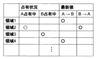
まず、共有メモリ上のデータ管理方法の例を、図5に示す。 First, an example of a data management method on a shared memory is shown in FIG.
本方式における必要事項は、ある処理が演算中のメモリ領域に、他の処理がアクセスすることを防ぐこと、および各処理が開始される際に適切な入力情報が書込まれているメモリ領域を渡すこと、の2点である。ここでの適切な入力情報とは、当該処理の開始時刻までに完了している、最新の相手処理の演算結果である。 The requirements for this method are to prevent other processes from accessing the memory area where a certain process is calculating, and to ensure that the memory area in which appropriate input information is written when each process starts. There are two points: passing it on. The appropriate input information here is the calculation result of the latest partner process that has been completed by the start time of the process.
前者は例えばメモリ上のデータ管理にはメモリ領域の占有状況として、後者はメモリ領域に格納された最新演算結果の位置として、それぞれ管理される。本例では、複数の処理が相互にデータを授受する構成であるため、最新演算結果は双方向に定義される。 For example, the former is managed as the occupancy status of the memory area for data management on the memory, and the latter is managed as the location of the latest calculation result stored in the memory area. In this example, since the configuration is such that a plurality of processes exchange data with each other, the latest calculation results are defined bidirectionally.
図6および図7を用いて、本実施例における処理A2開始時(時刻T1)におけるミドルウェア挙動を説明する。時刻T1においては、メモリ領域3が処理B2により占有されている。また、処理A1および処理B1が、当該時刻の開始時刻までに完了した最新の処理となるため、処理A1に関してはメモリ領域1および4が、処理B1に関してはメモリ領域2が、それぞれ最新処理結果であることが示される。本例では前述のように、処理Aの周期が処理Bより長いことから、処理Aは複数個所に演算結果を保存している。
Middleware behavior at the start of process A 2 (time T 1 ) in this embodiment will be explained using FIGS. 6 and 7. At time T1 ,
時刻T1にて起動される処理A2に対し、ミドルウェアは図7の管理テーブルにおける最新処理結果の列のうち、処理Bから処理Aの項目を検索する。結果、領域2に最新処理結果(処理B1の演算結果)が記載されていることから、当該領域が処理A2の利用すべき領域と分かる。そこで、管理テーブルにおける処理Aによる占有状況欄のメモリ領域2部分にチェック(図7の点線の丸)を入れ、当該メモリ領域のアドレスを処理Aに渡すことで処理A2を起動する。
For process A 2 started at time T 1 , the middleware searches for items from process B to process A in the latest process result column in the management table of FIG. 7 . As a result, since the latest processing result (calculation result of process B1 ) is written in
次に、時刻T2にて処理B2が終了した際の挙動を図8および図9を用いて説明する。図8に示すように、同時刻において処理A2は継続していること、および当該時刻での最新演算結果が処理B2の結果となることから、処理B2が占有していたメモリ領域3が最新の演算結果を保持している領域と分かる。
Next, the behavior when processing B 2 ends at time T 2 will be described using FIGS. 8 and 9. As shown in FIG. 8, since process A 2 continues at the same time and the latest calculation result at that time is the result of process B 2 , the
そこで、処理Bによる占有状況テーブルからメモリ領域3のチェックを外し、代わりに処理B→処理Aへの最新値テーブルの領域3の箇所にチェックを入れる。これにより、メモリ管理テーブルが図9のように更新される。このように管理テーブルが更新されることで、時刻T2直後に別の処理Aが起動された場合には、メモリ領域3を用いることで処理Bの最新処理結果を用いた演算を行うことが可能となる。
Therefore,
次に、各処理間でデータ授受に使うメモリ領域が不足した際に共有メモリ上に新たなメモリ領域を作成することでデータ授受を維持する方法について、図10および図11を用いて説明する。 Next, a method for maintaining data exchange by creating a new memory area on the shared memory when the memory area used for data exchange between each process runs out will be explained using FIGS. 10 and 11.
図10に示した時刻T0は、処理Aにおいて演算結果の書込みが開始されたタイミングである。前述のように、処理Aは処理Bに対して長い周期と定義されており、処理Aから処理Bへのデータ授受については複数のメモリ領域を備える必要がある。そこで、処理Aは複数のメモリ領域を確保する必要があるが、同タイミングにおいて確保されているメモリ領域は領域1のみであるため、ミドルウェアを通じて新たな書込み先を確保する必要がある。
Time T 0 shown in FIG. 10 is the timing at which writing of the calculation results in process A is started. As mentioned above, process A is defined to have a longer cycle than process B, and for data exchange from process A to process B, it is necessary to provide multiple memory areas. Therefore, process A needs to secure multiple memory areas, but since
そこで、ミドルウェアは図11の管理テーブルを参照するが、確保されているメモリ領域1およびメモリ領域3は処理A1、処理B2にそれぞれ占有されており、またメモリ領域2には処理Bの最新処理結果が格納されていることから、処理A1が新たに確保することができるメモリ領域が存在しない。そこで、新たに共有メモリの一部(処理A1の書込みサイズに相当)を処理A-処理B間のデータ授受用メモリ領域として確保および管理テーブル上の占有状態をAと更新し、メモリ領域4を作成する。このメモリ領域4を処理Aに渡すことで、処理A1の終了時には処理Aの最新値が両メモリ領域に書込まれた状態となる。
Therefore, the middleware refers to the management table in Figure 11, but the reserved
以上の構成によりミドルウェアを用いた上述のメモリ管理方式が提供され、先述の同じ周期の処理A、B間において2つのメモリ領域を用いたデータ授受を行った場合と同様、処理Aと処理B間でのデータコピーオーバヘッドは削減される。 With the above configuration, the above-mentioned memory management method using middleware is provided, and in the same way as when data is exchanged between processes A and B in the same cycle using two memory areas, data copy overhead is reduced.
また、産業用電子制御装置においては、一定の制御周期に沿って動作するアクチュエータを駆動する観点から、各処理、もしくは一連の複数処理に対する実行時間制約(リアルタイム制約)が存在する。これに違反した場合、アクチュエータ制御指令値が出力されない、もしくはセンサ入力値に対して適切でない指令値が出力される可能性があるため、アクチュエータに対応した未完了時処理が必要となる。例えば、冗長系構成を用いた別系統を利用した制御継続方式や、縮退制御方式などが挙げられる。 In addition, in industrial electronic control devices, there are execution time constraints (real-time constraints) for each process or a series of multiple processes from the viewpoint of driving actuators that operate according to a fixed control cycle. If this is violated, an actuator control command value may not be output, or a command value that is inappropriate for the sensor input value may be output, so incomplete processing corresponding to the actuator is required. Examples include a control continuation method using a separate system with a redundant system configuration, and a degeneration control method.
本構成においては、アプリケーション処理の終了予定時刻が設計時に規定されていることから、このタイミングまでに処理が完了しないケースに対して前述の未完了処理が実行される。未完了処理実施の要否をミドルウェアが判別するためには、例えばミドルウェアが処理を起動する際にフラグをセットし、処理の完了時にこのフラグを解除することで、処理終了時刻においてミドルウェアがチェックするような実装が考えられる。 In this configuration, since the scheduled end time of the application process is specified at the time of design, the above-mentioned incomplete process is executed in the case where the process is not completed by this timing. In order for the middleware to determine whether it is necessary to perform an unfinished process, for example, the middleware sets a flag when starting the process, releases this flag when the process is completed, and the middleware checks the flag at the process end time. An implementation like this is possible.
以上の構成を実現するミドルウェア挙動について、図12のフローチャートを用いて説明する。ミドルウェアは前述のように各処理の起動時刻に合わせる形で動作するため、例えば処理開始時刻のタイマ割込みにより起動される。換言すれば、複数の処理のそれぞれの開始時刻においてタイマ割込みが入る。その後、管理テーブルから最新処理結果格納先を探索し(S100)、当該領域を確保するため管理テーブルの占有状況箇所を更新する(S101)。 The middleware behavior that implements the above configuration will be explained using the flowchart in FIG. 12. Since the middleware operates in accordance with the start time of each process as described above, it is started, for example, by a timer interrupt at the process start time. In other words, a timer interrupt is generated at the start time of each of the plurality of processes. Thereafter, the latest processing result storage location is searched from the management table (S100), and the occupancy status location in the management table is updated to secure the area (S101).
そして、当該メモリ領域を処理に渡して処理を起動することで、アプリケーション処理が開始される(S102)。ここで、アプリケーション処理の周期の長短により、複数のメモリ領域へデータを書込む必要があり、かつそのような書込み先領域が確保されていない場合には新たなメモリ領域を確保し(S103)、管理表にアドレスを追加(S104)、当該書込み先の状態を占有中に変更した上で(S105)、処理に渡す(S106)。 Then, the application process is started by passing the memory area to the process and activating the process (S102). Here, if it is necessary to write data to multiple memory areas depending on the length of the application processing cycle, and such a write destination area is not secured, a new memory area is secured (S103), The address is added to the management table (S104), the state of the write destination is changed to occupied (S105), and the address is passed to processing (S106).
書込み先領域がミドルウェアにより既に確保され管理テーブルに記載されている場合は、S103およびS104をスキップし、S105が実施される。そして、アプリケーション処理終了時刻には開始時と同様にタイマ割込みが入る。換言すれば、複数の処理のそれぞれの終了時刻においてタイマ割込みが入る。アプリケーション処理終了時においては、メモリ管理テーブルの最新値状態を更新し(S107)、メモリ占有状態を解除する(S108)。以上により、1つのアプリケーション処理に対するミドルウェア処理が完結する。 If the write destination area has already been secured by the middleware and is listed in the management table, S103 and S104 are skipped and S105 is executed. Then, at the end time of the application process, a timer interrupt is generated in the same way as at the start time. In other words, a timer interrupt is generated at the end time of each of the plurality of processes. At the end of application processing, the latest value state of the memory management table is updated (S107), and the memory occupied state is released (S108). With the above, middleware processing for one application process is completed.
換言すれば、本実施例の電子制御装置は、異なる周期で動作する複数の処理を実行する複数のコア(CPUコア2)を含むプロセッサ(マルチコアプロセッサ1)と、複数の処理を実行する前記複数のコア(CPUコア2)ごとにそれぞれアクセス可能な複数のメモリ領域を含むメモリ(共有メモリ)と、を備え、データ書込みを行う先行処理とデータ読出しを行う後続処理とがそれぞれアクセス可能な前記メモリ領域を処理の進捗に応じて変更する。プロセッサ(マルチコアプロセッサ1)は、最新の処理の結果が書き込まれておらず、かつ読出し中でない書込み可能なメモリ領域を探索し、書込み可能なメモリ領域が存在しない場合、新たなメモリ領域を確保し、新たなメモリ領域を処理の結果の書き込み先とすることで、先行処理から後続処理へ処理の結果を受け渡す。 In other words, the electronic control device of this embodiment includes a processor (multi-core processor 1) including a plurality of cores (CPU core 2) that execute a plurality of processes that operate at different cycles, and a a memory (shared memory) including a plurality of memory areas that can be accessed by each core (CPU core 2), and the memory can be accessed by a preceding process for writing data and a subsequent process for reading data. Change the area according to the progress of processing. The processor (multi-core processor 1) searches for a writable memory area in which the result of the latest processing has not been written and is not being read, and if a writable memory area does not exist, allocates a new memory area. , by setting a new memory area as the writing destination of the processing results, the processing results are passed from the preceding processing to the succeeding processing.
図5に示すように、電子制御装置は、メモリ領域ごとの占有状況と処理の結果の最新値の有無を格納するテーブルを備える。プロセッサは、このテーブルのすべてのメモリ領域について、占有状況が専有を示し、または最新値の有無が最新値を格納していることを示す場合、書込み可能な前記メモリ領域が存在しないと判定する。 As shown in FIG. 5, the electronic control device includes a table that stores the occupancy status of each memory area and the presence or absence of the latest value of the processing result. The processor determines that the writable memory area does not exist when the occupancy status of all the memory areas in this table indicates exclusive use, or the presence or absence of the latest value indicates that the latest value is stored.
以上の構成により、マルチコアCPUにおける設計、開発、検証工数を低減する時刻同期型タイミング設計方式を低時間オーバヘッドに実現し、かつ異なるハードウェア(プロセッサ)間での移植性向上を実現する方式が提供される。 The above configuration provides a time-synchronized timing design method that reduces design, development, and verification man-hours for multi-core CPUs with low time overhead, and provides a method that improves portability between different hardware (processors). be done.
(実施例2)
以下、本発明に係る第2の実施例について図面を用いて説明する。想定するCPU構成(図1)や適用する時刻同期型タイミング設計方式(図2)は実施例1に準拠するが、本実施例では複数の処理Aおよび処理Bの間に一方向のデータ依存関係があるケース、すなわち処理Aの実行結果を利用して処理Bが実行されるが、逆は存在しないケースにおける本発明の適用事例を、主に実施例1との差分に着目して説明する。
(Example 2)
A second embodiment of the present invention will be described below with reference to the drawings. The assumed CPU configuration (Figure 1) and the applied time-synchronized timing design method (Figure 2) are based on Example 1, but in this example, there is a unidirectional data dependency relationship between multiple processes A and B. An application example of the present invention in a certain case, that is, a case in which process B is executed using the execution result of process A, but the reverse does not exist, will be described, focusing mainly on the differences from Example 1.
本実施例においては、処理B実行に必要な処理Aの演算結果のみを共有メモリ上に展開することで、例えば処理Aへの入力データといった処理B実行に不要なデータを共有メモリ上に複数保持する必要がなく、処理間のメモリ利用効率の向上および、これに伴う制御装置内におけるメモリ利用効率向上、最終的には制御装置に搭載するメモリサイズ低減による低コスト化が期待される。 In this example, by deploying only the calculation results of process A necessary for executing process B onto the shared memory, multiple pieces of data that are unnecessary for executing process B, such as input data to process A, are retained on the shared memory. There is no need to do this, and it is expected to improve memory usage efficiency between processes, improve memory usage efficiency within the control device, and ultimately reduce costs by reducing the memory size installed in the control device.
図13に、本発明が例題とする処理構成を示す。本実施例では、メモリ領域は3つの異なるメモリ領域(領域1~3)から構成される。前述のように、本実施例においては、処理Aの演算結果を処理Bが読込む構成となっていることから、図中の共有メモリ領域記載においては、処理Aは自身の演算結果の書込みのみ、処理Bは処理Aの演算結果の読込みのみ、をそれぞれ記載している。
FIG. 13 shows a processing configuration taken as an example of the present invention. In this embodiment, the memory area is composed of three different memory areas (
処理Aが自身の演算に用いる読込データや、処理Bが自身の演算結果を書込む領域については、図中の共有メモリ領域に書込む構成をとることも、それ以外のデータ依存関係を有する処理との間で同様の共有メモリ構成をとることも、可能である。 The area where process A writes the read data used for its own calculations and the area where process B writes its own calculation results can be configured to write to the shared memory area shown in the figure, or other processes with data dependencies It is also possible to have a similar shared memory configuration between
このような共有メモリの利用方式においては、処理A、Bの2つの処理間でデータ共有する場合については、処理Aの書込み先が2箇所(処理Aの周期が処理Bの周期より短い場合)と、処理Bの読出し先が1ヶ所の合計3箇所以上あれば、実施例1に記載のデータ受渡し(1つの処理が書込みもしくは読出しのいずれかのみを担当する)が可能となる。 In this shared memory usage method, when data is shared between two processes, Process A and B, Process A writes to two locations (if Process A's cycle is shorter than Process B's cycle). If the number of read destinations of process B is three or more in total, the data transfer described in the first embodiment (one process is responsible for either writing or reading only) becomes possible.
なお、本実施例のような構成については、図14に示したように、処理Aの周期が処理Bの周期に対して更に小さくなる場合についても、同様のメモリ構成をとることが可能である。このように、処理Bの周期が、処理Aの周期の2倍以上となったケースについては、実施例1に示したメモリ管理表において、最新値ではないメモリ領域に処理結果が上書きされることで、共有メモリ領域の更なる追加が不要となる。 Note that, regarding the configuration of this embodiment, as shown in FIG. 14, it is possible to use a similar memory configuration even when the cycle of process A becomes smaller than the cycle of process B. . In this way, in the case where the cycle of process B is twice or more than the cycle of process A, the process result will be overwritten in the memory area that does not have the latest value in the memory management table shown in Example 1. Therefore, there is no need to further add a shared memory area.
例えば、処理A1の演算結果Res(A1)が処理Bにより読出される前に処理A2が演算完了するため、処理B2には処理A2の演算結果Res(A2 )が読出されればよい。そのため、同図に示したように、処理A3の演算結果Res(A3)は、メモリ領域2にある処理A1の演算結果Res(A1)を上書きすることが許容される。
For example, since processing A 2 completes its calculation before processing A 1 's calculation result Res(A 1 ) is read by process B, processing A 2 's calculation result Res(A 2 ) is not read into process B 2 . That's fine. Therefore, as shown in the figure, the calculation result Res(A 3 ) of process A 3 is allowed to overwrite the calculation result Res(A 1 ) of process A 1 in
逆に、処理Aの周期が処理Bの周期より長いケースにおいても、処理Bが自身が読出すメモリ領域に自身の演算結果を上書きしない限りにおいて、図15に示すように同様の構成をとることが可能となる。 Conversely, even in the case where the cycle of process A is longer than the cycle of process B, the same configuration as shown in FIG. 15 can be adopted as long as process B does not overwrite its own calculation results in the memory area that it reads. becomes possible.
以上の構成、すなわちデータ受け渡しが発生する2つの処理間において、1つの処理が書込みのみ、もう1つの処理は読出しのみ、を担当する場合については、本実施例のように3つの共有メモリ領域のみを用いることで、実施例1の事例に比べ、必要メモリ量の削減およびミドルウェア(もしくは、実装形態によりOS、各アプリケーション)におけるメモリ領域の追加判定処理が不要となり、実装の効率化が図られる。 In the above configuration, where one process is responsible for only writing and the other process is only for reading between two processes where data is exchanged, only three shared memory areas are required as in this example. By using this, compared to the case of Example 1, the required memory amount is reduced and the process of determining the addition of a memory area in the middleware (or the OS or each application depending on the implementation form) becomes unnecessary, and the implementation becomes more efficient.
(実施例3)
以下、本発明に係る第3の実施例について図面を用いて説明する。
(Example 3)
A third embodiment of the present invention will be described below with reference to the drawings.
図16に、本発明が例題とする処理構成を示す。本例においては、実施例2と同様に処理Aは書込みのみを、処理Bは読出しのみを行う構成ではあるが、Aの処理区間とAの周期とが不一致な場合を例として説明する。時刻同期型のタイミング設計方式においては、前述のように必ずしも処理区間と周期とが一致する必要はないため、このような構成をとることが可能となる。 FIG. 16 shows a processing configuration taken as an example of the present invention. In this example, as in the second embodiment, processing A is configured to perform only writing, and processing B is configured to perform only reading, but a case will be described as an example in which the processing section of A and the cycle of A do not match. In the time-synchronized timing design method, such a configuration is possible because the processing interval and the cycle do not necessarily have to match as described above.
このようなケースにおいては、同図に示したように、処理A3の演算結果Res(A3 )が読みだされる前に処理A4が完了し、処理B4には処理A4の演算結果Res(A4 )を用いて演算を開始することができる。この場合、実施例1および2とは異なり、共有メモリ領域の利用率が低下し、メモリ効率の悪化が発生する。 In such a case, as shown in the figure, process A 4 is completed before the calculation result Res(A 3 ) of process A 3 is read, and process B 4 includes the calculation result of process A 4 . The result Res(A 4 ) can be used to start the operation. In this case, unlike the first and second embodiments, the usage rate of the shared memory area decreases, resulting in deterioration of memory efficiency.
そこで、共有メモリ上には(同一周期の場合と同様に)最低限必要な2つのメモリ領域を構成し、3つめのメモリ領域は必要に応じて共有メモリから動的に確保し、不要と判別された場合には解放することで、制御装置全体の処理構成の間で予備領域を融通し、メモリ効率を更に向上することが可能となる。 Therefore, the minimum required two memory areas are configured on the shared memory (as in the case of the same cycle), the third memory area is dynamically allocated from the shared memory as needed, and the third memory area is determined to be unnecessary. By releasing the reserved area when the reserved area is released, the spare area can be used among the processing components of the entire control device, and memory efficiency can be further improved.
換言すれば、本実施例では、メモリ領域は2つの異なるメモリ領域から構成され、プロセッサ(マルチコアプロセッサ1)は、書込み可能なメモリ領域が存在しない場合、新たなメモリ領域を確保する。その後、例えば、メモリ領域として3つ以上のメモリアドレスを有している条件において、プロセッサ(マルチコアプロセッサ1)は、1つのメモリアドレスが最新の処理の結果の書込み先ではなく、かつ読出し中でもない場合において、前記1つのメモリアドレスを解放する。 In other words, in this embodiment, the memory area is composed of two different memory areas, and if a writable memory area does not exist, the processor (multi-core processor 1) secures a new memory area. After that, for example, in a condition where the memory area has three or more memory addresses, the processor (multi-core processor 1) determines if one memory address is not the writing destination for the latest processing result and is not currently being read. In this step, the one memory address is released.
以上の構成を、ミドルウェアによりメモリ管理により実現する方式を示す。本実施例では、メモリ領域の管理処理は、プロセッサ(マルチコアプロセッサ1)が専用のミドルウェアを実行することにより実現される。なお、実施例1と同様、本実施例で説明するミドルウェア処理はOSや各処理内部にて実施されても良い。 A method for realizing the above configuration through memory management using middleware is shown below. In this embodiment, the memory area management process is realized by the processor (multi-core processor 1) executing dedicated middleware. Note that, similar to the first embodiment, the middleware processing described in this embodiment may be implemented within the OS or each process.
予備領域の確保については、実施例1に説明した構成と同様のもので実現可能であるため、本実施例においては予備領域の解放処理について説明する。 Since securing of the spare area can be realized using a configuration similar to that described in the first embodiment, in this embodiment, the process of releasing the spare area will be described.
前述のように、予備領域が不要となるケースについて図17から図19を用いて説明する。図17における時刻T3直前(処理A4の処理区間終了直前)においては、図18のようにメモリ領域1は処理A4がメモリ領域2を占有、また処理A3の結果が最新値となっている。
As mentioned above, the case where the spare area is unnecessary will be explained using FIGS. 17 to 19. Immediately before time T 3 in FIG. 17 (immediately before the end of the processing section of process A 4 ), in
時刻T3直後のメモリ状態は図19のようになっており、メモリ領域2がB占有中かつ最新処理結果が書き込まれており、予備領域は空欄となる。このように処理A4の完了に伴い、予備領域が占有されておらず、かつ最新値が書き込まれていないケースにおいて、予備領域の解放が可能となる。処理Aの周期が処理Bより長い場合においては、最新値が書き込まれておらず、かつ処理Aが予備領域を占有する必要がない場合に、同領域が解放可能となる。
The memory state immediately after time T3 is as shown in FIG. 19, in which
以上のことから、ミドルウェア処理では、処理の開始時にメモリ解放可能かを判別する構成をとることで、全てのケースに対して適用が可能となる(処理Aの周期が処理Bより短い場合は、次の処理A起動時まではオーバヘッドが継続する)。 From the above, middleware processing can be applied to all cases by having a configuration that determines whether memory can be released at the start of the process (if the cycle of process A is shorter than process B, (The overhead continues until the next process A is started.)
図20に、このようなミドルウェア挙動フローを示す。基本的な構成は実施例1にと同様だが、処理Aおよび処理Bは書込みもしくは読出し処理のいずれかを行うため、この判別機構によりフローが少々異なっている。そのため、処理起動時に、読出し処理か書込み処理化の条件分岐が入る。以降は実施例1のミドルウェア処理を踏襲する。本例において追加となるのは、書込み処理側において書込み可能領域が存在した場合である。この際に、管理メモリ領域数が3つ以上であり、かつ、予備領域が最新値を保持しておらず読出し中でもない場合に、解放可能となり、メモリ領域を管理表から削除する(S109)。 FIG. 20 shows such a middleware behavior flow. The basic configuration is the same as in the first embodiment, but since Process A and Process B perform either write or read processing, the flow is slightly different depending on this discrimination mechanism. Therefore, at the time of processing start-up, a conditional branch for either read processing or write processing is entered. From now on, the middleware processing of the first embodiment is followed. In this example, the addition occurs when a writable area exists on the write processing side. At this time, if the number of managed memory areas is three or more and the spare area does not hold the latest value and is not being read, the memory area can be released and the memory area is deleted from the management table (S109).
なお、本例では処理間でのデータ受渡し用に用いる固定的な2つのメモリ領域と、必要に応じて動的に確保/解放する1つの予備領域を用いる例について説明したが、2つのメモリ領域が常に確保されるのであれば、前述の固定的なメモリ領域としての形態は不要である。 Note that in this example, we have explained an example using two fixed memory areas used for passing data between processes and one reserve area that is dynamically allocated/released as needed. If it is always secured, the above-mentioned form as a fixed memory area is unnecessary.
すなわち、常に管理テーブル上に確保される2つのメモリ領域と、さらに必要に応じて動的に確保/解放される1つのメモリ領域、の構成でも、本実施例は実現可能である。この場合には、管理メモリ領域の解放条件は、管理アドレスが3つ以上であり、かつ、最新値を保持せず読出し中でもない、場合において、管理表からアドレス削除を行うことが可能となる。この場合には、S109処理が、当該メモリ領域を探索し削除、と変化する。 That is, the present embodiment can be realized even with a configuration of two memory areas that are always reserved on the management table and one memory area that is dynamically reserved/released as needed. In this case, the conditions for releasing the management memory area are that there are three or more management addresses, and the latest value is not held or being read, and addresses can be deleted from the management table. In this case, the process in S109 changes to search for and delete the memory area.
(実施例4)
以下、本発明に係る第4の実施例について図面を用いて説明する。
(Example 4)
A fourth embodiment of the present invention will be described below with reference to the drawings.
産業系電子制御装置はセンサ情報の入力に基づき制御指令値を演算しアクチュエータを制御する構成が取られる。このような構成においては、周期的に動作するアクチュエータを正しく制御するため、一般的にセンサ入力から制御指令値出力までの間に実行時間制約が存在する。 Industrial electronic control devices are configured to calculate control command values based on sensor information input and control actuators. In such a configuration, in order to properly control the actuator that operates periodically, there is generally an execution time constraint between the sensor input and the control command value output.
一方で、マルチコア/メニーコアCPUにおける設計においては、前述の複数コア間におけるソフトウェア挙動は実行時のプロセッサ状態に応じて容易に変化し得ることから、例えば実行時間の変動が発生する。このような実行時間変動に対して、設計時におけるマージン設計などによる対処が取られるが、実行時間制約の厳しさや各種資源の競合により必ずしも処理完了が保証されるとは限らない。そのため、ミドルウェアに処理完了の確認と、未完了時の対処が必要となる。 On the other hand, in designing a multi-core/many-core CPU, the software behavior among the multiple cores described above can easily change depending on the processor state at the time of execution, resulting in variations in execution time, for example. Measures are taken to deal with such fluctuations in execution time, such as margin design during design, but processing completion is not always guaranteed due to the severity of execution time constraints and competition for various resources. Therefore, the middleware needs to confirm that the process is completed and take action if it is not completed.
図21に、処理Aの図中2回目の実行である処理A2が、実行時間変動の影響により規定の処理区間内に処理を完了できなかった例を示す。 FIG. 21 shows an example in which process A2 , which is the second execution of process A in the diagram, could not be completed within a specified process interval due to the influence of execution time fluctuation.
本時刻同期型タイミング設計方式における、処理未完了時の対処としては以下の2つの方式が想定される。1つは、処理A2を強制的に中断もしくは実行終了させるケースである。対処法としては上位システムへ通知を行い、判断を仰ぐケースや、設計時にこのような違反発生ケースに対する処理が規定され、そちらに移行するケースも考えられるが、制御目的や実行時間制約違反時の影響範囲が小さいケースにおいては処理を継続するケースも想定される。 In this time-synchronized timing design method, the following two methods are assumed to be used when processing is not completed. One is a case where processing A2 is forcibly interrupted or terminated. As a countermeasure, there are cases in which a notification is sent to the upper system and a decision is made, and there are also cases in which a process for such violation cases is specified at the design stage and the process is moved to that direction, but for control purposes or when execution time constraints are violated. In cases where the scope of influence is small, it is assumed that processing will continue.
このような場合、ミドルウェアでは処理A2を中止し、かつメモリ管理テーブルを更新しないことで、処理A2の演算結果Res(A2)を用いるはずであった処理B4および処理B5が、演算未完了な値を用いないように制御する。これら処理は、処理A1の演算結果Res(A1)を用いて制御を継続する。 In such a case, the middleware cancels process A 2 and does not update the memory management table, so that process B 4 and process B 5 , which were supposed to use the calculation result Res(A 2 ) of process A 2 , Control so that uncompleted values are not used. These processes continue to be controlled using the calculation result Res(A 1 ) of process A 1 .
換言すれば、ミドルウェアを実行するプロセッサ(マルチコアプロセッサ1)は、複数の処理のそれぞれの終了時刻において、処理未完了を検出した場合に強制的に当該処理を停止させる未完了処理を行う。 In other words, when the processor (multi-core processor 1) that executes the middleware detects that a process is incomplete at the end time of each of a plurality of processes, it performs an incomplete process that forcibly stops the process.
もう1つの方式は、このようなケースにおいて、処理Aに対する処理Bのような、先行処理の結果を用いて処理を行う後続処理の設計時マージンを用いて処理Aの実行時間を延長することで、後続処理Bに最新の処理結果を渡す方式である。 Another method is to extend the execution time of process A in such cases by using the design time margin of a subsequent process that uses the results of a preceding process, such as process B for process A. , the latest processing result is passed to subsequent processing B.
換言すれば、ミドルウェアを実行するプロセッサ(マルチコアプロセッサ1)は、複数の処理のそれぞれの終了時刻において、処理未完了を検出した場合において、当該処理の演算結果を用いて演算を行う後続処理の開始時刻を、設計時に規定される猶予時間分だけ遅らせることにより、後続処理において最新の演算処理結果を用いて演算を継続する。 In other words, when the processor (multi-core processor 1) that executes the middleware detects that a process is incomplete at the end time of each of a plurality of processes, it starts a subsequent process that performs a calculation using the calculation result of the process. By delaying the time by a grace period specified at the time of design, calculations are continued using the latest calculation results in subsequent processing.
図21において、処理A2の後続処理である処理B4、およびコア数によっては処理A2の遅れの影響が自身の処理時間削減に繋がる処理A3の両者は、共にマージン時間、すなわち処理区間と各処理の実行時間との差分が存在する。この時間は通常、前述のようなマルチコア上における実行時間変動を吸収するために用いられるものであるが、設計時における最悪実行時間が常に発生するわけではないことから、同マージン時間を利用することは可能である。 In FIG. 21, both process B 4 , which is the subsequent process of process A 2 , and process A 3 , where the influence of the delay of process A 2 can reduce its own processing time depending on the number of cores, both have a margin time, that is, a processing interval. There is a difference between the execution time of each process and the execution time of each process. This time is usually used to absorb the variation in execution time on multi-cores as described above, but since the worst execution time does not always occur at design time, the same margin time can be used. is possible.
本実施例においては、例えばマージン時間を最悪実行時間+20%と設計し、そのうち10%をこのような先行処理の遅れに対し適用可能であるとする。このような時間を、遅延吸収時間(図22)と呼ぶと、このような条件において、処理A2に遅延が発生した場合、影響を受ける処理(処理B4、および例えば2コアで本処理を行う場合には処理A3も含む)のうち、直近の遅延吸収時間終了時刻(同図における時刻T4)を、ミドルウェアがタスク情報などから取得し、同時刻まで処理A2を継続する。同時刻において処理A2が完了した場合には実施例3に記載のメモリ管理と同様の終了処理を実施し、同時刻においても処理A2が完了しない場合には、前述の1つめの方式と同様の強制終了処理を取る。 In this embodiment, it is assumed that the margin time is designed to be, for example, the worst execution time +20%, and 10% of the margin time can be applied to such a delay in advance processing. This time is called delay absorption time (Figure 22). Under these conditions, if a delay occurs in process A 2 , the affected process (process B 4 and, for example, this process with 2 cores) If processing A 3 is also included), the middleware acquires the most recent delay absorption time end time (time T 4 in the figure) from task information, etc., and continues processing A 2 until the same time. If process A 2 is completed at the same time, the same termination process as the memory management described in Example 3 is performed, and if process A 2 is not completed at the same time, the first method described above is used. Perform the same forced termination process.
図23に、本実施例におけるミドルウェア挙動に関するフロー図を示す。上述の未完了時処理(S110)を追加することで、産業用制御装置に求められる実行時間制約に関し、特に制約違反の検出および対処方式が提供され、より幅広い産業用制御装置への本方式適用が実現される。 FIG. 23 shows a flow diagram regarding middleware behavior in this embodiment. By adding the above-mentioned incomplete processing (S110), a method for detecting and dealing with violation of constraints is provided, especially regarding the execution time constraints required for industrial control equipment, and this method can be applied to a wider range of industrial control equipment. is realized.
以上の構成により、産業用制御装置に求められる実時間制約に対し、本発明が準拠することが出来る。また上記に示した2つめの対処法においては、実時間制約に違反した場合においても、処理実行上のマージン時間を用いて対処可能となる場合において処理継続もしくは最新の処理結果を用いた処理継続を可能とすることで、産業用制御装置による制御演算継続およびその精度向上が実現される。 With the above configuration, the present invention can comply with real-time constraints required of industrial control devices. In addition, in the second solution shown above, even if the real time constraint is violated, processing can be continued if it is possible to deal with it using the processing execution margin time, or processing can be continued using the latest processing results. By making this possible, it is possible to continue control calculations by the industrial control device and improve its accuracy.
以上説明したように、第1~第4の実施例によれば、時刻同期型設計におけるアプリケーション間におけるデータ受渡の効率を高めることができる。 As described above, according to the first to fourth embodiments, it is possible to improve the efficiency of data transfer between applications in a time-synchronized design.
なお、本発明は上記した実施例に限定されるものではなく、様々な変形例が含まれる。例えば、上述した実施例は本発明を分かりやすく説明するために詳細に説明したものであり、必ずしも説明した全ての構成を備えるものに限定されるものではない。また、ある実施例の構成の一部を他の実施例の構成に置き換えることが可能であり、また、ある実施例の構成に他の実施例の構成を加えることも可能である。また、各実施例の構成の一部について、他の構成の追加・削除・置換をすることが可能である。 Note that the present invention is not limited to the above-described embodiments, and includes various modifications. For example, the embodiments described above are described in detail to explain the present invention in an easy-to-understand manner, and the present invention is not necessarily limited to having all the configurations described. Furthermore, it is possible to replace a part of the configuration of one embodiment with the configuration of another embodiment, and it is also possible to add the configuration of another embodiment to the configuration of one embodiment. Further, it is possible to add, delete, or replace a part of the configuration of each embodiment with other configurations.
また、上記の各構成、機能等は、それらの一部又は全部を、例えば集積回路で設計する等によりハードウェアで実現してもよい。また、上記の各構成、機能等は、プロセッサがそれぞれの機能を実現するプログラムを解釈し、実行することによりソフトウェアで実現してもよい。各機能を実現するプログラム、テーブル、ファイル等の情報は、メモリや、ハードディスク、SSD(Solid State Drive)等の記録装置、または、ICカード、SDカード、DVD等の記録媒体に置くことができる。 Further, each of the configurations, functions, etc. described above may be partially or entirely realized by hardware, for example, by designing an integrated circuit. Furthermore, each of the above configurations, functions, etc. may be realized by software by a processor interpreting and executing a program for realizing each function. Information such as programs, tables, files, etc. that realize each function can be stored in a memory, a recording device such as a hard disk, an SSD (Solid State Drive), or a recording medium such as an IC card, an SD card, or a DVD.
なお、本発明の実施例は、以下の態様であってもよい。 In addition, the following aspects may be sufficient as the Example of this invention.
複数のコアを含むプロセッサを有する電子制御装置であって、前記プロセッサは、異なる周期で動作する複数の処理を実行し、前記複数の処理を実行する前記複数のコアごとにそれぞれアクセス可能な複数のメモリ領域を備え、データ書込みを行う先行処理と、データ読出しを行う後続処理とがそれぞれアクセス可能な前記メモリ領域を、前記処理の進捗に応じて変更する電子制御装置において、最新の前記処理の結果が書き込まれておらず、かつ読出し中でない書込み可能な前記メモリ領域を探索し、書込み可能な前記メモリ領域が存在しない場合、新たな前記メモリ領域を確保し、新たな前記メモリ領域を前記処理の結果の書き込み先とすることで、前記先行処理から前記後続処理へ前記処理の結果を受け渡すこと、を特徴とする電子制御装置。 An electronic control device having a processor including a plurality of cores, wherein the processor executes a plurality of processes that operate at different cycles, and has a plurality of processors each of which is accessible to each of the plurality of cores that execute the plurality of processes. In an electronic control device that includes a memory area and changes the memory area that can be accessed by a preceding process for writing data and a subsequent process for reading data, depending on the progress of the process, the latest result of the process. The writable memory area that has not been written to and is not being read is searched, and if the writable memory area does not exist, a new memory area is secured, and the new memory area is used for the process. An electronic control device characterized in that the results of the processing are passed from the preceding processing to the subsequent processing by being set as a write destination of the results.
これにより、産業用制御装置に求められる時刻同期型設計におけるアプリケーション間におけるデータ受渡の効率を高めることが可能である。 This makes it possible to improve the efficiency of data transfer between applications in the time-synchronized design required for industrial control devices.
1:マルチコアプロセッサ
2:CPUコア
21:L1キャッシュ
22:L2キャッシュ
3:内部バス
4:外部メモリ
5:センサ
1: Multi-core processor 2: CPU core 21: L1 cache 22: L2 cache 3: Internal bus 4: External memory 5: Sensor
Claims (9)
前記複数の処理を実行する前記複数のコアごとにそれぞれアクセス可能な複数のメモリ領域を含むメモリと、を備え、
データ書込みを行う先行処理とデータ読出しを行う後続処理とがそれぞれアクセス可能な前記メモリ領域を前記処理の進捗に応じて変更する電子制御装置であって、
前記プロセッサは、
最新の前記処理の結果が書き込まれておらず、かつ読出し中でない書込み可能な前記メモリ領域を探索し、書込み可能な前記メモリ領域が存在しない場合、新たな前記メモリ領域を確保し、新たな前記メモリ領域を前記処理の結果の書き込み先とすることで、前記先行処理から前記後続処理へ前記処理の結果を受け渡すこと、を特徴とする電子制御装置。 A processor that includes multiple cores that execute multiple processes that operate at different cycles;
a memory including a plurality of memory areas that can be accessed by each of the plurality of cores that execute the plurality of processes,
An electronic control device that changes the memory area that can be accessed by a preceding process for writing data and a subsequent process for reading data according to the progress of the process,
The processor includes:
The writable memory area in which the latest result of the process has not been written and is not being read is searched, and if the writable memory area does not exist, a new memory area is secured and the new memory area is searched. An electronic control device characterized in that the results of the processing are passed from the preceding processing to the subsequent processing by setting a memory area as a writing destination of the results of the processing.
前記複数の処理のそれぞれの開始時刻および終了時刻においてタイマ割込みが入ること、を特徴とする電子制御装置。 The electronic control device according to claim 1,
An electronic control device characterized in that a timer interrupt is generated at the start time and end time of each of the plurality of processes.
前記メモリ領域は3つの異なるメモリ領域から構成されること、を特徴とする電子制御装置。 The electronic control device according to claim 2,
An electronic control device characterized in that the memory area is composed of three different memory areas.
前記メモリ領域は2つの異なるメモリ領域から構成され、
前記プロセッサは、
書込み可能な前記メモリ領域が存在しない場合、新たな前記メモリ領域を確保すること、を特徴とする電子制御装置。 The electronic control device according to claim 2,
The memory area is composed of two different memory areas,
The processor includes:
An electronic control device characterized in that, if the writable memory area does not exist, a new memory area is secured.
前記メモリ領域として3つ以上のメモリアドレスを有している条件において、
前記プロセッサは、
1つのメモリアドレスが最新の前記処理の結果の書込み先ではなく、かつ読出し中でもない場合において、前記1つのメモリアドレスを解放すること、を特徴とする電子制御装置。 The electronic control device according to claim 4,
Under the condition that the memory area has three or more memory addresses,
The processor includes:
An electronic control device characterized in that the one memory address is released when the one memory address is not a writing destination of the latest result of the processing and is not being read.
前記メモリ領域の管理処理は、
前記プロセッサが専用のミドルウェアを実行することにより実現されること、を特徴とする電子制御装置。 The electronic control device according to claim 1,
The memory area management process includes:
An electronic control device characterized in that the processor executes dedicated middleware.
前記ミドルウェアを実行する前記プロセッサは、
前記複数の処理のそれぞれの終了時刻において、処理未完了を検出した場合に強制的に当該処理を停止させる未完了処理を行うこと、を特徴とする電子制御装置。 The electronic control device according to claim 6,
The processor that executes the middleware includes:
An electronic control device characterized in that, at the end time of each of the plurality of processes, when an incomplete process is detected, an incomplete process is performed to forcibly stop the process.
前記ミドルウェアを実行する前記プロセッサは、
前記複数の処理のそれぞれの終了時刻において、処理未完了を検出した場合において、当該処理の演算結果を用いて演算を行う後続処理の開始時刻を、設計時に規定される猶予時間分だけ遅らせることにより、後続処理において最新の演算処理結果を用いて演算を継続すること、を特徴とする電子制御装置。 The electronic control device according to claim 6,
The processor that executes the middleware includes:
When it is detected that a process is incomplete at the end time of each of the plurality of processes, the start time of a subsequent process that performs a calculation using the calculation result of the process is delayed by a grace period specified at the time of design. An electronic control device characterized in that, in subsequent processing, calculation is continued using the latest calculation processing result.
前記メモリ領域ごとの占有状況と前記処理の結果の最新値の有無を格納するテーブルを備え、
前記プロセッサは、
前記テーブルのすべての前記メモリ領域について、前記占有状況が専有を示し、または前記最新値の有無が最新値を格納していることを示す場合、書込み可能な前記メモリ領域が存在しないと判定すること、を特徴とする電子制御装置。 The electronic control device according to claim 1,
comprising a table storing the occupancy status of each memory area and the presence or absence of the latest value of the result of the processing,
The processor includes:
For all the memory areas of the table, if the occupancy status indicates exclusive, or the presence or absence of the latest value indicates that the latest value is stored, determining that the writable memory area does not exist. An electronic control device characterized by.
Priority Applications (2)
| Application Number | Priority Date | Filing Date | Title |
|---|---|---|---|
| JP2020117161A JP7425685B2 (en) | 2020-07-07 | 2020-07-07 | electronic control unit |
| PCT/JP2021/024626 WO2022009741A1 (en) | 2020-07-07 | 2021-06-29 | Electronic control device |
Applications Claiming Priority (1)
| Application Number | Priority Date | Filing Date | Title |
|---|---|---|---|
| JP2020117161A JP7425685B2 (en) | 2020-07-07 | 2020-07-07 | electronic control unit |
Publications (3)
| Publication Number | Publication Date |
|---|---|
| JP2022014679A JP2022014679A (en) | 2022-01-20 |
| JP2022014679A5 JP2022014679A5 (en) | 2023-02-06 |
| JP7425685B2 true JP7425685B2 (en) | 2024-01-31 |
Family
ID=79553102
Family Applications (1)
| Application Number | Title | Priority Date | Filing Date |
|---|---|---|---|
| JP2020117161A Active JP7425685B2 (en) | 2020-07-07 | 2020-07-07 | electronic control unit |
Country Status (2)
| Country | Link |
|---|---|
| JP (1) | JP7425685B2 (en) |
| WO (1) | WO2022009741A1 (en) |
Families Citing this family (2)
| Publication number | Priority date | Publication date | Assignee | Title |
|---|---|---|---|---|
| JP2023161698A (en) * | 2022-04-26 | 2023-11-08 | 日立Astemo株式会社 | Electronic control device |
| CN115878549A (en) * | 2023-03-03 | 2023-03-31 | 上海聪链信息科技有限公司 | Inter-core communication system |
Citations (2)
| Publication number | Priority date | Publication date | Assignee | Title |
|---|---|---|---|---|
| WO2010119932A1 (en) | 2009-04-17 | 2010-10-21 | 日本電気株式会社 | Multi-processor system, and memory management method and communication program in multi-processor system |
| JP2010244096A (en) | 2009-04-01 | 2010-10-28 | Seiko Epson Corp | Data processing apparatus, printing system, and program |
-
2020
- 2020-07-07 JP JP2020117161A patent/JP7425685B2/en active Active
-
2021
- 2021-06-29 WO PCT/JP2021/024626 patent/WO2022009741A1/en active Application Filing
Patent Citations (2)
| Publication number | Priority date | Publication date | Assignee | Title |
|---|---|---|---|---|
| JP2010244096A (en) | 2009-04-01 | 2010-10-28 | Seiko Epson Corp | Data processing apparatus, printing system, and program |
| WO2010119932A1 (en) | 2009-04-17 | 2010-10-21 | 日本電気株式会社 | Multi-processor system, and memory management method and communication program in multi-processor system |
Also Published As
| Publication number | Publication date |
|---|---|
| WO2022009741A1 (en) | 2022-01-13 |
| JP2022014679A (en) | 2022-01-20 |
Similar Documents
| Publication | Publication Date | Title |
|---|---|---|
| CN109997112B (en) | Data processing | |
| EP3531292B1 (en) | Methods and apparatus for supporting persistent memory | |
| US8473950B2 (en) | Parallel nested transactions | |
| US7543295B2 (en) | Method for enhancing efficiency in mutual exclusion | |
| US7805582B2 (en) | Method of managing memory in multiprocessor system on chip | |
| US11132294B2 (en) | Real-time replicating garbage collection | |
| US5825649A (en) | Kernel substitution method in multi-processor system and multi-processor system having kernel substitution function | |
| JP7425685B2 (en) | electronic control unit | |
| CN111857993B (en) | Method for calling user mode function in kernel mode | |
| WO2005048010A2 (en) | Method and system for minimizing thread switching overheads and memory usage in multithreaded processing using floating threads | |
| CN111666210A (en) | Chip verification method and device | |
| US8954969B2 (en) | File system object node management | |
| CN103329102A (en) | Multiprocessor system | |
| US20200272512A1 (en) | Hardware for supporting os driven observation and anticipation based on more granular, variable sized observation units | |
| JPWO2010097925A1 (en) | Information processing device | |
| CN114780248A (en) | Resource access method, device, computer equipment and storage medium | |
| JP5999216B2 (en) | Data processing device | |
| JP2000029691A (en) | Data processor | |
| JP2005521937A (en) | Context switching method and apparatus in computer operating system | |
| JP7204443B2 (en) | VEHICLE CONTROL DEVICE AND PROGRAM EXECUTION METHOD | |
| CN111831327A (en) | Electronic device capable of executing instructions and instruction execution method | |
| EP2176761A1 (en) | Object model for transactional memory | |
| JP7078380B2 (en) | Instruction control device, instruction control method and program | |
| JP4755232B2 (en) | compiler | |
| US20050251795A1 (en) | Method, system, and program for optimizing code |
Legal Events
| Date | Code | Title | Description |
|---|---|---|---|
| A521 | Request for written amendment filed |
Free format text: JAPANESE INTERMEDIATE CODE: A523 Effective date: 20230127 |
|
| A621 | Written request for application examination |
Free format text: JAPANESE INTERMEDIATE CODE: A621 Effective date: 20230127 |
|
| TRDD | Decision of grant or rejection written | ||
| A01 | Written decision to grant a patent or to grant a registration (utility model) |
Free format text: JAPANESE INTERMEDIATE CODE: A01 Effective date: 20240116 |
|
| A61 | First payment of annual fees (during grant procedure) |
Free format text: JAPANESE INTERMEDIATE CODE: A61 Effective date: 20240119 |
|
| R150 | Certificate of patent or registration of utility model |
Ref document number: 7425685 Country of ref document: JP Free format text: JAPANESE INTERMEDIATE CODE: R150 |