JP7417455B2 - Electronic devices and their control methods and programs - Google Patents

Electronic devices and their control methods and programs Download PDF

Info

Publication number
JP7417455B2
JP7417455B2 JP2020058306A JP2020058306A JP7417455B2 JP 7417455 B2 JP7417455 B2 JP 7417455B2 JP 2020058306 A JP2020058306 A JP 2020058306A JP 2020058306 A JP2020058306 A JP 2020058306A JP 7417455 B2 JP7417455 B2 JP 7417455B2
Authority
JP
Japan
Prior art keywords
data
reading
electronic device
commands
command group
Prior art date
Legal status (The legal status is an assumption and is not a legal conclusion. Google has not performed a legal analysis and makes no representation as to the accuracy of the status listed.)
Active
Application number
JP2020058306A
Other languages
Japanese (ja)
Other versions
JP2021157599A (en
Inventor
達也 渡邉
Current Assignee (The listed assignees may be inaccurate. Google has not performed a legal analysis and makes no representation or warranty as to the accuracy of the list.)
Canon Inc
Original Assignee
Canon Inc
Priority date (The priority date is an assumption and is not a legal conclusion. Google has not performed a legal analysis and makes no representation as to the accuracy of the date listed.)
Filing date
Publication date
Application filed by Canon Inc filed Critical Canon Inc
Priority to JP2020058306A priority Critical patent/JP7417455B2/en
Priority to US17/211,620 priority patent/US12086081B2/en
Publication of JP2021157599A publication Critical patent/JP2021157599A/en
Application granted granted Critical
Publication of JP7417455B2 publication Critical patent/JP7417455B2/en
Active legal-status Critical Current
Anticipated expiration legal-status Critical

Links

Images

Classifications

    • GPHYSICS
    • G06COMPUTING; CALCULATING OR COUNTING
    • G06FELECTRIC DIGITAL DATA PROCESSING
    • G06F13/00Interconnection of, or transfer of information or other signals between, memories, input/output devices or central processing units
    • G06F13/14Handling requests for interconnection or transfer
    • G06F13/16Handling requests for interconnection or transfer for access to memory bus
    • G06F13/1668Details of memory controller
    • GPHYSICS
    • G06COMPUTING; CALCULATING OR COUNTING
    • G06FELECTRIC DIGITAL DATA PROCESSING
    • G06F13/00Interconnection of, or transfer of information or other signals between, memories, input/output devices or central processing units
    • G06F13/10Program control for peripheral devices
    • G06F13/12Program control for peripheral devices using hardware independent of the central processor, e.g. channel or peripheral processor
    • G06F13/124Program control for peripheral devices using hardware independent of the central processor, e.g. channel or peripheral processor where hardware is a sequential transfer control unit, e.g. microprocessor, peripheral processor or state-machine
    • GPHYSICS
    • G06COMPUTING; CALCULATING OR COUNTING
    • G06FELECTRIC DIGITAL DATA PROCESSING
    • G06F3/00Input arrangements for transferring data to be processed into a form capable of being handled by the computer; Output arrangements for transferring data from processing unit to output unit, e.g. interface arrangements
    • G06F3/06Digital input from, or digital output to, record carriers, e.g. RAID, emulated record carriers or networked record carriers
    • G06F3/0601Interfaces specially adapted for storage systems
    • G06F3/0602Interfaces specially adapted for storage systems specifically adapted to achieve a particular effect
    • G06F3/0604Improving or facilitating administration, e.g. storage management
    • GPHYSICS
    • G06COMPUTING; CALCULATING OR COUNTING
    • G06TIMAGE DATA PROCESSING OR GENERATION, IN GENERAL
    • G06T1/00General purpose image data processing
    • G06T1/60Memory management
    • GPHYSICS
    • G06COMPUTING; CALCULATING OR COUNTING
    • G06FELECTRIC DIGITAL DATA PROCESSING
    • G06F3/00Input arrangements for transferring data to be processed into a form capable of being handled by the computer; Output arrangements for transferring data from processing unit to output unit, e.g. interface arrangements
    • G06F3/06Digital input from, or digital output to, record carriers, e.g. RAID, emulated record carriers or networked record carriers
    • G06F3/0601Interfaces specially adapted for storage systems
    • G06F3/0628Interfaces specially adapted for storage systems making use of a particular technique
    • G06F3/0655Vertical data movement, i.e. input-output transfer; data movement between one or more hosts and one or more storage devices
    • G06F3/0659Command handling arrangements, e.g. command buffers, queues, command scheduling
    • GPHYSICS
    • G06COMPUTING; CALCULATING OR COUNTING
    • G06FELECTRIC DIGITAL DATA PROCESSING
    • G06F3/00Input arrangements for transferring data to be processed into a form capable of being handled by the computer; Output arrangements for transferring data from processing unit to output unit, e.g. interface arrangements
    • G06F3/06Digital input from, or digital output to, record carriers, e.g. RAID, emulated record carriers or networked record carriers
    • G06F3/0601Interfaces specially adapted for storage systems
    • G06F3/0668Interfaces specially adapted for storage systems adopting a particular infrastructure
    • G06F3/0671In-line storage system
    • G06F3/0673Single storage device

Landscapes

  • Engineering & Computer Science (AREA)
  • Theoretical Computer Science (AREA)
  • Physics & Mathematics (AREA)
  • General Physics & Mathematics (AREA)
  • General Engineering & Computer Science (AREA)
  • Human Computer Interaction (AREA)
  • Computer Hardware Design (AREA)
  • Microelectronics & Electronic Packaging (AREA)
  • Studio Devices (AREA)

Description

本発明は、着脱可能デバイスと接続可能な電子機器及びその制御方法、プログラムに関する。 The present invention relates to an electronic device connectable to a removable device, a control method thereof, and a program.

近年、監視カメラにより撮像された画像を用いて物体の検出や追尾、属性の推定等を行う画像解析、そのような画像解析の結果を用いた物体数の推定が様々なシーンで行われている。これまでは監視カメラの映像をPCやサーバ等の高性能な演算装置に転送して画像解析が行われてきたが、モバイル用演算装置の処理能力の向上に伴い、画像解析をカメラ側で直接行う事例も増えてきている。実装形態としてはカメラ本体に演算装置を配置する他に、USB等の着脱可能デバイスに演算装置を配置する形態も提案されている。カメラ本体に演算装置を配置した形態では、演算装置を配置した着脱可能デバイスを装着することで、カメラ側でより高度な解析処理を行うことができる。 In recent years, image analysis that uses images captured by surveillance cameras to detect and track objects, estimate attributes, etc., and estimation of the number of objects using the results of such image analysis has been performed in a variety of situations. . Up until now, image analysis has been performed by transmitting images from surveillance cameras to high-performance computing devices such as PCs and servers, but as the processing power of mobile computing devices has improved, image analysis has been performed directly on the camera side. The number of cases in which this is done is increasing. In addition to arranging the arithmetic device in the camera body, other implementations have also been proposed in which the arithmetic device is placed in a removable device such as a USB. In a configuration in which a computing device is disposed in the camera body, more advanced analysis processing can be performed on the camera side by attaching a removable device in which the computing device is disposed.

しかし、汎用的なI/Fを用いてカメラと着脱可能デバイスを接続した場合、通信に用いられるプロトコルは公知である。そのため、データを容易に解析されてしまう可能性がある。特許文献1では、通信を確立する際に暗号化を用いて通信設定のための情報を交換する通信設定方式が開示されている。また、特許文献2では複数のI/F(複数の通信経路)で機器間を接続し、通信経路の数で暗号化した情報を復元する方法が開示されている。 However, when a camera and a removable device are connected using a general-purpose I/F, the protocol used for communication is well known. Therefore, the data may be easily analyzed. Patent Document 1 discloses a communication setting method that uses encryption to exchange information for communication settings when establishing communication. Further, Patent Document 2 discloses a method of connecting devices through multiple I/Fs (multiple communication paths) and restoring information encrypted using the number of communication paths.

特開2015-046927号公報Japanese Patent Application Publication No. 2015-046927 特開2013-144037号公報Japanese Patent Application Publication No. 2013-144037

しかしながら、上述の特許文献1に開示された従来技術では、通信方法を確立するための認証方法に関しては記載があるが、通信確立後のデータの送受信方式に関しては言及されていない。また、上述の特許文献2に開示された従来技術では、データを暗号化するための方法に関しては記載があるが、機器間のI/Fのプロトコル自体が解析されることに関しては言及されていない。 However, in the prior art disclosed in Patent Document 1 mentioned above, although there is a description of an authentication method for establishing a communication method, there is no mention of a data transmission/reception method after communication is established. Further, the conventional technology disclosed in Patent Document 2 mentioned above describes a method for encrypting data, but does not mention that the I/F protocol itself between devices is analyzed. .

本発明は、既知の通信プロトコルを用いて接続された電子機器とデバイスの間の通信内容が第三者により把握されてしまう可能性を低減する技術を提供する。 The present invention provides a technique for reducing the possibility that a third party will understand the contents of communication between an electronic device and a device connected using a known communication protocol.

本発明の一態様による電子機器は以下の構成を備える。すなわち、
演算処理部を備えたデバイスを着脱可能な電子機器であって、
前記演算処理部の処理対象であるデータを分割して複数の分割データを得る分割手段と、
前記複数の分割データの各々を前記デバイスへ送信するための、複数種類のコマンドの組み合わせである第1のコマンド群を決定する決定手段と、
前記決定手段により決定された前記第1のコマンド群を用いて分割データを送信する送信手段と、を備え、
前記決定手段は、前記複数の分割データの内のある分割データを送信する場合と、他の分割データを送信する場合とで、前記第1のコマンド群を構成するコマンドの組み合わせを変更する。
An electronic device according to one embodiment of the present invention has the following configuration. That is,
An electronic device to which a device equipped with an arithmetic processing unit can be attached and detached,
dividing means for dividing the data to be processed by the arithmetic processing unit to obtain a plurality of divided data;
determining means for determining a first command group that is a combination of multiple types of commands for transmitting each of the plurality of divided data to the device;
transmitting means for transmitting divided data using the first command group determined by the determining means,
The determining means changes the combination of commands constituting the first command group depending on when transmitting one of the plurality of divided data and when transmitting another divided data.

本発明によれば、既知の通信プロトコルを用いて接続された電子機器とデバイスの間の通信内容が第三者により把握されてしまう可能性を低減することができる。 According to the present invention, it is possible to reduce the possibility that a third party will understand the contents of communication between an electronic device and a device that are connected using a known communication protocol.

実施形態によるシステム構成の一例を示す図。FIG. 1 is a diagram showing an example of a system configuration according to an embodiment. 撮像装置のハードウェア構成例を示すブロック図。FIG. 2 is a block diagram showing an example of the hardware configuration of an imaging device. 撮像装置の機能構成例を示すブロック図。FIG. 2 is a block diagram showing an example of a functional configuration of an imaging device. 着脱可能デバイスのハードウェア構成例を示すブロック図。FIG. 2 is a block diagram showing an example of a hardware configuration of a removable device. 着脱可能デバイスの機能構成例を示すブロック図。FIG. 2 is a block diagram showing an example of a functional configuration of a removable device. システムで実行される処理の例を示すフローチャート。Flowchart showing an example of processing performed by the system. コマンドとレスポンスの構造を示す図。A diagram showing the structure of commands and responses. 第1実施形態による分割画像データの生成例を示した図。FIG. 3 is a diagram showing an example of generation of divided image data according to the first embodiment. 第1実施形態による画像送信処理を示すフローチャート。5 is a flowchart showing image transmission processing according to the first embodiment. 第1実施形態による演算結果の受信処理を示すフローチャート。5 is a flowchart illustrating processing for receiving calculation results according to the first embodiment. 第2実施形態による、複数フレームの送受信処理を示したフローチャート。7 is a flowchart showing a process for transmitting and receiving multiple frames according to the second embodiment. 理機能の情報を格納しているアドレス内のデータを概略的に示す図。FIG. 3 is a diagram schematically showing data within an address that stores information about a physical function. 撮像装置が取得する情報の例を示す図。FIG. 3 is a diagram illustrating an example of information acquired by an imaging device.

以下、添付図面を参照して実施形態を詳しく説明する。なお、以下の実施形態は特許請求の範囲に係る発明を限定するものではない。実施形態には複数の特徴が記載されているが、これらの複数の特徴の全てが発明に必須のものとは限らず、また、複数の特徴は任意に組み合わせられてもよい。さらに、添付図面においては、同一若しくは同様の構成に同一の参照番号を付し、重複した説明は省略する。 Hereinafter, embodiments will be described in detail with reference to the accompanying drawings. Note that the following embodiments do not limit the claimed invention. Although a plurality of features are described in the embodiments, not all of these features are essential to the invention, and the plurality of features may be arbitrarily combined. Furthermore, in the accompanying drawings, the same or similar components are designated by the same reference numerals, and redundant description will be omitted.

[第1実施形態]
以下、着脱可能なデバイスを装着する電子機器として撮像装置を用いた例を説明する。
<システム構成>
図1に、本実施形態の画像解析システムの構成例を示す。以下では、一例として、このシステムが特定人物追跡システムである場合について説明する。ただし、これに限られず、画像を解析して所定の情報出力を行う任意のシステムに、以下の議論を適用することができる。本システムは、撮像装置110a~110dと、ネットワーク120と、入出力装置130とを含んで構成される。なお、撮像装置110a~110dは、それぞれ、例えば撮像した画像を記録可能なデバイスを着脱可能なスロットを有し、そのスロットに着脱可能デバイス100a~100dが挿入されることにより、着脱可能デバイス100a~100dと接続される。なお、以下では、着脱可能デバイス100a~100dを「着脱可能デバイス100」と表記し、撮像装置110a~110dを「撮像装置110」と表記する。なお、以下では、画像という用語は、映像、動画、静止画を総称するものとする。
[First embodiment]
Hereinafter, an example will be described in which an imaging device is used as an electronic device to which a removable device is attached.
<System configuration>
FIG. 1 shows an example of the configuration of an image analysis system according to this embodiment. Below, as an example, a case where this system is a specific person tracking system will be described. However, the present invention is not limited to this, and the following discussion can be applied to any system that analyzes images and outputs predetermined information. This system includes imaging devices 110a to 110d, a network 120, and an input/output device 130. Note that each of the imaging devices 110a to 110d has a slot into which a device capable of recording a captured image can be attached and detached, and by inserting the detachable device 100a to 100d into the slot, the detachable device 100a to 100d can be inserted into the slot. Connected to 100d. Note that, hereinafter, the removable devices 100a to 100d will be referred to as "removable devices 100," and the imaging devices 110a to 110d will be referred to as "imaging devices 110." Note that in the following, the term "image" shall collectively refer to video, moving images, and still images.

着脱可能デバイス100は、撮像装置110に対して着脱可能な演算デバイスである。着脱可能デバイス100は、一例として、SDカードに所定の処理回路を搭載したメモリデバイスである。着脱可能デバイス100は、例えば、SDカードの態様によって、撮像装置110にその全体が挿入可能に構成され、これにより、撮像装置110から突出する部分がない状態で撮像装置110と接続可能に構成することができる。また、着脱可能デバイス100は、例えば、撮像装置110にその半分以上の部分が挿入可能に構成され、これにより、撮像装置110から突出する部分が少ない状態で撮像装置110と接続可能に構成されてもよい。これにより、着脱可能デバイス100が配線等の障害物と干渉することを防ぐことができ、デバイスの利用時の利便性を高めることができる。また、多くの既存のネットワークカメラなどの撮像装置110には、SDカードスロットが用意されているため、既存の撮像装置110に対して、着脱可能デバイス100により拡張機能を提供することができる。なお、着脱可能デバイス100は、SDカードの態様以外に、少なくともその撮像装置110で撮影された画像を記憶可能な記憶装置が装着される際に使用される任意のインタフェースで、撮像装置110に装着されるように構成されてもよい。例えば、着脱可能デバイス100は、USB(ユニバーサリシリアルバス)インタフェースを有し、撮像装置110のUSBソケットに装着されるように構成されてもよい。また、所定の処理回路は、例えば、所定の処理を実行するようにプログラムされたFPGA(フィールドプログラマブルゲートアレイ)によって実装されるが、それ以外の形式で実装されてもよい。 The removable device 100 is a computing device that is removable from the imaging device 110. The removable device 100 is, for example, a memory device in which a predetermined processing circuit is mounted on an SD card. The removable device 100 is configured such that it can be inserted in its entirety into the imaging device 110 in the form of an SD card, for example, so that it can be connected to the imaging device 110 without any portion protruding from the imaging device 110. be able to. Further, the removable device 100 is configured such that half or more of the portion thereof can be inserted into the imaging device 110, for example, so that it can be connected to the imaging device 110 with a small portion protruding from the imaging device 110. Good too. This can prevent the removable device 100 from interfering with obstacles such as wiring, and can improve the convenience of using the device. Further, since many existing imaging devices 110 such as network cameras are provided with an SD card slot, the removable device 100 can provide extended functionality to the existing imaging device 110. Note that the removable device 100 can be attached to the imaging device 110 using any interface used when a storage device capable of storing at least images captured by the imaging device 110 is attached, other than an SD card. It may be configured so that For example, the removable device 100 may have a USB (Universal Serial Bus) interface and be configured to be attached to a USB socket of the imaging device 110. Further, the predetermined processing circuit is implemented, for example, by an FPGA (field programmable gate array) programmed to execute a predetermined process, but may be implemented in other formats.

撮像装置110は、ネットワークカメラ等の撮像装置である。本実施形態では、撮像装置110は、画像を処理することのできる演算装置を内蔵するものとするが、これに限られない。例えば、撮像装置110に接続されたPC(パーソナルコンピュータ)等の外部コンピュータが存在してもよく、これらの組み合わせを、撮像装置110として扱ってもよい。また、本実施形態では、全ての撮像装置110に、着脱可能デバイス100が装着されているものとする。なお、図1では、4つの撮像装置110と、それぞれに装着された着脱可能デバイスとが示されているが、これらの装置の組み合わせの数は3つ以下であってもよいし、5つ以上であってもよい。撮像装置110に、画像解析処理機能を有する着脱可能デバイス100が装着されることにより、撮像装置110が画像解析処理機能を有しなくても、撮像装置110側で画像処理を実行することが可能となる。また、本実施形態のように撮像装置110に画像処理用の演算装置が配置された形態では、演算装置が配置された着脱可能デバイス100が撮像装置110に装着されることにより、撮像装置110側で実行可能な画像処理を多様化・高度化することができる。 The imaging device 110 is an imaging device such as a network camera. In this embodiment, it is assumed that the imaging device 110 includes a built-in arithmetic device that can process images, but the present invention is not limited to this. For example, there may be an external computer such as a PC (personal computer) connected to the imaging device 110, and a combination of these may be treated as the imaging device 110. Further, in this embodiment, it is assumed that the removable device 100 is attached to all the imaging devices 110. Note that although FIG. 1 shows four imaging devices 110 and removable devices attached to each, the number of combinations of these devices may be three or less, or five or more. It may be. By attaching the removable device 100 having an image analysis processing function to the imaging device 110, it is possible to perform image processing on the imaging device 110 side even if the imaging device 110 does not have an image analysis processing function. becomes. Furthermore, in a configuration in which a computing device for image processing is arranged in the imaging device 110 as in the present embodiment, the removable device 100 in which the computing device is arranged is attached to the imaging device 110, so that the imaging device 110 side The image processing that can be performed can be diversified and sophisticated.

入出力装置130は、ユーザからの入力の受け付けや、ユーザへの情報の出力(例えば情報の表示)を行う装置である。本実施形態では、例えば入出力装置130は、PC等のコンピュータであり、そのコンピュータにインストールされたブラウザやネイティブアプリケーションによって、情報の入出力が行われる。 The input/output device 130 is a device that receives input from a user and outputs information to the user (for example, displays information). In this embodiment, for example, the input/output device 130 is a computer such as a PC, and information is input/output using a browser or native application installed on the computer.

撮像装置110と入出力装置130は、ネットワーク120を介して通信可能に接続される。ネットワーク120は、例えばEthernet(登録商標)等の通信規格を満たす複数のルータ、スイッチ、ケーブル等を含んで構成される。本実施形態では、ネットワーク120は、撮像装置110と入出力装置130との間の通信を可能とする任意のネットワークであってよく、任意の規模や構成、準拠する通信規格によって構築されうる。例えば、ネットワーク120は、インターネットや有線LAN(Local Area Network)、無線LAN、WAN(Wide Area Network)等でありうる。また、ネットワーク120は、例えば、ONVIF(Open Network Video Interface Forum)規格に準拠した通信プロトコルでの通信が可能なように構成されうる。ただし、これに限られず、ネットワーク120は、例えば、独自の通信プロトコル等の他の通信プロトコルでの通信が可能なように構成されてもよい。 The imaging device 110 and the input/output device 130 are communicably connected via the network 120. The network 120 includes a plurality of routers, switches, cables, etc. that meet communication standards such as, for example, Ethernet (registered trademark). In the present embodiment, the network 120 may be any network that enables communication between the imaging device 110 and the input/output device 130, and may be constructed in any size and configuration, and according to a compliant communication standard. For example, the network 120 may be the Internet, a wired LAN (Local Area Network), a wireless LAN, a WAN (Wide Area Network), or the like. Further, the network 120 may be configured to enable communication using a communication protocol that conforms to the ONVIF (Open Network Video Interface Forum) standard, for example. However, the present invention is not limited thereto, and the network 120 may be configured to enable communication using other communication protocols, such as a proprietary communication protocol.

<装置構成>
(撮像装置の構成)
続いて、撮像装置110の構成について説明する。図2は、撮像装置110のハードウェア構成例を示す図である。撮像装置110は、そのハードウェア構成として、例えば、撮像部201、画像処理部202、演算処理部203、配信部204、SD I/F部205を含む。なお、I/Fは、インタフェースの略語である。
<Device configuration>
(Configuration of imaging device)
Next, the configuration of the imaging device 110 will be described. FIG. 2 is a diagram showing an example of the hardware configuration of the imaging device 110. The imaging device 110 includes, as its hardware configuration, an imaging section 201, an image processing section 202, an arithmetic processing section 203, a distribution section 204, and an SD I/F section 205, for example. Note that I/F is an abbreviation for interface.

撮像部201は、光を結像するためのレンズ部と、結像された光に応じたアナログ信号変換する撮像素子とを含んで構成される。レンズ部は、画角を調整するズーム機能や、光量の調整を行う絞り機能などを有する。撮像素子は、光をアナログ信号に変換する際の感度調整を行うゲイン機能を有する。これらの機能は、画像処理部202から通知された設定値に基づいて調整される。撮像部201によって取得されたアナログ信号は、アナログ-デジタル変換回路によってデジタル信号に変換され、画像信号として画像処理部202へ転送される。 The imaging unit 201 includes a lens unit for forming an image of light, and an image sensor that converts an analog signal according to the imaged light. The lens section has a zoom function that adjusts the angle of view, an aperture function that adjusts the amount of light, and the like. The image sensor has a gain function that adjusts sensitivity when converting light into an analog signal. These functions are adjusted based on the setting values notified from the image processing unit 202. The analog signal acquired by the imaging unit 201 is converted into a digital signal by an analog-to-digital conversion circuit and transferred to the image processing unit 202 as an image signal.

画像処理部202は、画像処理エンジンと、その周辺デバイス等を含んで構成される。周辺デバイスは、例えば、RAM(Random Access Memory)や、各I/Fのドライバ等を含む。画像処理部202では、撮像部201から取得した画像信号に対して、例えば、現像処理、フィルタ処理、センサ補正、ノイズ除去等の、画像処理を施して画像データを生成する。また、画像処理部202は、レンズ部や撮像素子へ設定値を送信し、適切露出画像を取得できるように、露出調整を実行しうる。画像処理部202において生成された画像データは、演算処理部203へ転送される。 The image processing unit 202 includes an image processing engine, its peripheral devices, and the like. Peripheral devices include, for example, RAM (Random Access Memory), drivers for each I/F, and the like. The image processing unit 202 performs image processing such as development processing, filter processing, sensor correction, and noise removal on the image signal acquired from the imaging unit 201 to generate image data. Further, the image processing unit 202 can transmit setting values to the lens unit and the image sensor, and perform exposure adjustment so that an appropriately exposed image can be obtained. Image data generated in the image processing section 202 is transferred to the arithmetic processing section 203.

演算処理部203は、CPUやMPU等の1つ以上のプロセッサ、RAMやROM等のメモリ、各I/Fのドライバなどから構成される。なお、CPUはCentral Processing Unitの、MPUはMicro Processing Unitの、RAMはRandom Access Memoryの、ROMはRead Only Memoryの、頭字語である。演算処理部203では、一例において、上述のシステムにおいて実行されるべき処理の各部分を撮像装置110と着脱可能デバイス100とのいずれが実行するかの分担を決定し、その決定した分担に対応する処理を実行しうる。また、演算処理部203は、着脱可能デバイス100とのSD規格(SD Associationにより策定)に則ったSD通信のプロトコル制御も行う。SD通信のプロトコル制御機能の詳細に関しては後述する。画像処理部202から受け取った画像は、配信部204、又は、SD I/F部205へ転送される。また、処理結果のデータも配信部204へ転送される。 The arithmetic processing unit 203 includes one or more processors such as a CPU or MPU, memory such as a RAM or ROM, drivers for each I/F, and the like. Note that CPU is an acronym for Central Processing Unit, MPU is for Micro Processing Unit, RAM is for Random Access Memory, and ROM is for Read Only Memory. In one example, the arithmetic processing unit 203 determines which of the imaging device 110 and the removable device 100 will perform each part of the processing to be executed in the above-described system, and performs processing corresponding to the determined division. Processing can be executed. The arithmetic processing unit 203 also performs protocol control for SD communication with the removable device 100 in accordance with the SD standard (defined by the SD Association). Details of the SD communication protocol control function will be described later. The image received from the image processing unit 202 is transferred to the distribution unit 204 or the SD I/F unit 205. Further, data of the processing result is also transferred to the distribution unit 204.

配信部204は、ネットワーク配信エンジンと、例えば、RAMやETH PHYモジュールなどの周辺デバイス等を含んで構成される。ETH PHYモジュールは、Ethernetの物理(PHY)レイヤの処理を実行するモジュールである。配信部204は、演算処理部203から取得した画像データや処理結果のデータを、ネットワーク120へ配信可能な形式に変換して、変換後のデータをネットワーク120へ出力する。SD I/F部205は、着脱可能デバイス100と接続するためのインタフェース部分で、例えば、電源と、着脱可能デバイス100を着脱するための、着脱ソケット等の装着機構を含んで構成される。ここでは、SD I/F部205が、SD Associationにより策定されたSD規格に従って構成されるものとする。演算処理部203から取得された画像の着脱可能デバイス100への転送や、着脱可能デバイス100からのデータの取得等の、着脱可能デバイス100と撮像装置110との間での通信は、SD I/F部205を通じて行われる。 The distribution unit 204 includes a network distribution engine and peripheral devices such as a RAM and an ETH PHY module. The ETH PHY module is a module that executes Ethernet physical (PHY) layer processing. The distribution unit 204 converts the image data and processing result data acquired from the arithmetic processing unit 203 into a format that can be distributed to the network 120, and outputs the converted data to the network 120. The SD I/F section 205 is an interface section for connecting with the removable device 100, and includes, for example, a power source and a mounting mechanism such as a detachable socket for attaching and detaching the detachable device 100. Here, it is assumed that the SD I/F section 205 is configured in accordance with the SD standard established by the SD Association. Communication between the removable device 100 and the imaging device 110, such as transferring images acquired from the arithmetic processing unit 203 to the removable device 100 and acquiring data from the removable device 100, is performed using the SD I/ This is done through the F unit 205.

図3に、撮像装置110の機能構成例を示す。撮像装置110は、その機能として、例えば、撮像制御部301、信号処理部302、記憶部303、制御部304、解析部305、デバイス通信部306、及び、ネットワーク通信部307を含む。 FIG. 3 shows an example of the functional configuration of the imaging device 110. The imaging device 110 includes, as its functions, an imaging control section 301, a signal processing section 302, a storage section 303, a control section 304, an analysis section 305, a device communication section 306, and a network communication section 307, for example.

撮像制御部301は、撮像部201を介して周囲の環境を撮影するようにする制御を実行する。信号処理部302は、撮像制御部301によって撮影された画像に対して所定の処理を施して、撮影画像のデータを生成する。以下では、この撮影画像のデータを単に「撮影画像」と呼ぶ。信号処理部302は、例えば、撮像制御部301によって撮影された画像を符号化する。信号処理部302は、静止画像に対して、例えば、JPEG(Joint Photographic Experts Group)等の符号化方式を用いて符号化を行う。また、信号処理部302は、動画像に対して、H.264/MPEG-4 AVC(以下では「H.264」と呼ぶ。)、HEVC(High Efficiency Video Coding)等の符号化方式を用いて符号化を行う。また、信号処理部302は、予め設定された複数の符号化方式の中から、例えば撮像装置110の不図示の操作部を介して、ユーザにより選択された符号化方式を用いて、画像を符号化してもよい。 The imaging control unit 301 executes control to photograph the surrounding environment via the imaging unit 201. The signal processing unit 302 performs predetermined processing on the image photographed by the imaging control unit 301 to generate data of the photographed image. Hereinafter, the data of this photographed image will simply be referred to as a "photographed image." The signal processing unit 302 encodes, for example, an image photographed by the imaging control unit 301. The signal processing unit 302 encodes the still image using, for example, an encoding method such as JPEG (Joint Photographic Experts Group). The signal processing unit 302 also processes H. Encoding is performed using an encoding method such as H.264/MPEG-4 AVC (hereinafter referred to as "H.264") or HEVC (High Efficiency Video Coding). Further, the signal processing unit 302 encodes the image using an encoding method selected by the user from among a plurality of preset encoding methods, for example, via an operation unit (not shown) of the imaging device 110. may be converted into

記憶部303は、後述する解析処理の結果を記憶する。なお、本実施形態では、実行される処理が解析処理であるが、任意の処理が実行されてもよい。制御部304は、信号処理部302、記憶部303、解析部305、デバイス通信部306、ネットワーク通信部307を、それぞれが所定の処理を実行するように、制御する。 The storage unit 303 stores the results of analysis processing, which will be described later. Note that in this embodiment, the process executed is an analysis process, but any process may be executed. The control unit 304 controls the signal processing unit 302, the storage unit 303, the analysis unit 305, the device communication unit 306, and the network communication unit 307 so that each of them executes a predetermined process.

解析部305は、撮影画像に対して、解析前処理、解析処理、解析後処理の少なくともいずれかを選択的に実行する。解析前処理は、後述の解析処理を実行する前に、撮影画像に対して実行する処理である。本実施形態の解析前処理では、一例として、撮影画像を分割して分割画像を作成する処理が実行されるものとする。解析処理は、入力された画像を解析して得られる情報を出力する処理である。本実施形態の解析処理では、一例として、解析前処理によって得られた分割画像を入力として、人体検出処理、顔検出処理、車両検出処理の少なくともいずれかを実行し、解析処理結果を出力する処理が実行されるものとする。解析処理は、例えば非特許文献1の技術によって、画像に含まれるオブジェクトを検出できるように学習が行われた機械学習モデルを用いて、分割画像中のオブジェクトの位置を出力するように構成された処理でありうる。解析後処理は、解析処理が実行された後に実行される処理である。本実施形態の解析後処理では、一例として、各分割画像に対する解析処理結果に基づいて、各分割画像において検出されたオブジェクトの数を合計した値を処理結果として出力する処理が実行されるものとする。なお、解析処理は、パターンマッチングを行って画像中のオブジェクトを検出し、その位置を出力する処理であってもよい。 The analysis unit 305 selectively performs at least one of pre-analysis processing, analysis processing, and post-analysis processing on the captured image. The pre-analysis process is a process that is performed on a photographed image before performing an analysis process that will be described later. In the analysis pre-processing of this embodiment, as an example, it is assumed that a process of dividing a captured image to create divided images is executed. The analysis process is a process of outputting information obtained by analyzing an input image. In the analysis processing of this embodiment, for example, the divided images obtained by the analysis preprocessing are input, and at least one of human body detection processing, face detection processing, and vehicle detection processing is executed, and the analysis processing results are output. shall be executed. The analysis process is configured to output the position of the object in the divided image using a machine learning model that has been trained to detect objects included in the image, for example, using the technology of Non-Patent Document 1. It can be a process. The post-analysis process is a process that is executed after the analysis process is executed. In the post-analysis processing of this embodiment, as an example, processing is executed to output the sum of the number of objects detected in each divided image as a processing result based on the analysis processing result for each divided image. do. Note that the analysis process may be a process of detecting an object in an image by performing pattern matching and outputting its position.

デバイス通信部306は、着脱可能デバイス100との通信を行う。デバイス通信部306は、入力されたデータを着脱可能デバイス100が処理可能な形式に変換し、その変換によって得られたデータを着脱可能デバイス100に送信する。また、デバイス通信部306は、着脱可能デバイス100からデータを受信し、受信したデータを撮像装置110が処理可能な形式に変換する。本実施形態では、デバイス通信部306は、変換処理として、小数を浮動小数点形式と固定小数点形式との間で変換する処理を実行するものとするが、これに限られず、他の処理がデバイス通信部306によって実行されてもよい。また、本実施形態では、デバイス通信部306は、着脱可能デバイス100に対してSD規格の範囲内で事前に定められたコマンドシーケンスを送信し、着脱可能デバイス100からの応答を受信することで、着脱可能デバイス100との通信を行うものとする。ネットワーク通信部307は、ネットワーク120を介して、入出力装置130との通信を行う。 The device communication unit 306 communicates with the detachable device 100. The device communication unit 306 converts the input data into a format that can be processed by the removable device 100 and transmits the data obtained by the conversion to the removable device 100. Further, the device communication unit 306 receives data from the removable device 100 and converts the received data into a format that can be processed by the imaging device 110. In this embodiment, it is assumed that the device communication unit 306 executes a process of converting a decimal number between a floating point format and a fixed point format as a conversion process, but the device communication unit 306 is not limited to this, and other processes may be performed for device communication. 306. Furthermore, in the present embodiment, the device communication unit 306 transmits a predetermined command sequence within the scope of the SD standard to the removable device 100, and receives a response from the removable device 100. It is assumed that communication with the removable device 100 is performed. The network communication unit 307 communicates with the input/output device 130 via the network 120.

(着脱可能デバイスの構成)
図4に、着脱可能デバイス100のハードウェア構成例を示す。着脱可能デバイス100は、一例として、I/F部401、FPGA402、SDコントローラ403、及び、記憶部404を含んで構成される。着脱可能デバイス100は、撮像装置110が有するSD I/F部205の着脱ソケットに挿抜できる形状で、すなわちSD規格に則った形状で成形されるものとする。
(Configuration of removable device)
FIG. 4 shows an example of the hardware configuration of the removable device 100. The detachable device 100 includes, for example, an I/F section 401, an FPGA 402, an SD controller 403, and a storage section 404. It is assumed that the removable device 100 is molded in a shape that can be inserted into and removed from a removable socket of the SD I/F section 205 of the imaging device 110, that is, in a shape that complies with the SD standard.

I/F部401は、撮像装置110等の装置と着脱可能デバイス100とを接続するためのインタフェース部分である。I/F部401は、例えば、撮像装置110から電源の供給を受け、着脱可能デバイス100内で使用する電源を生成し分配する、電気的な接点端子等を含んで構成される。I/F部401は、撮像装置110のSD I/F部205と同様に、SD規格内で定義(準拠)されている項目に関しては、それに従うものとする。撮像装置110からの画像や設定データの受け取り、FPGA402から撮像装置110へのデータの送信は、I/F部401を介して実行される。 The I/F section 401 is an interface section for connecting a device such as the imaging device 110 and the removable device 100. The I/F unit 401 is configured to include, for example, electrical contact terminals that receive power from the imaging device 110, generate and distribute power to be used within the detachable device 100. Like the SD I/F unit 205 of the imaging device 110, the I/F unit 401 complies with the items defined (conforms) within the SD standard. Reception of images and setting data from the imaging device 110 and transmission of data from the FPGA 402 to the imaging device 110 are performed via the I/F unit 401.

FPGA402は、入出力制御部410、処理切替部411、及び演算処理部412を含んで構成される。FPGA402は、内部の論理回路構造を繰り返し再構成できる半導体デバイスの一種である。FPGA402が実現する処理により、着脱可能デバイス100が装着された装置に、処理機能を追加(提供)することができる。また、FPGA402の再構成機能により、後から論理回路構造を変更することができるため、例えば技術の進歩の早い分野の装置に着脱可能デバイス100を装着することにより、その装置において適時に適切な処理を実行することが可能となる。なお、本実施形態では、FPGAが用いられる例について説明するが、後述する処理を実現可能である限りにおいて、例えば、汎用のASICや専用のLSIが用いられてもよい。FPGA402は、生成される論理回路構造の情報を含んだ設定データが専用のI/Fから書き込まれることにより、又は、その設定データがその専用のI/Fから読み出されることによって、起動される。本実施形態では、この設定データが記憶部404に保持されているものとする。FPGA402は、電源が投入されると、記憶部404から設定データを読み出し、論理回路を生成して起動する。ただし、これに限られず、例えば、着脱可能デバイス内に専用の回路を実装することにより、I/F部401を介して、撮像装置110がFPGA402に設定データを書き込んでもよい。 The FPGA 402 includes an input/output control section 410, a processing switching section 411, and an arithmetic processing section 412. The FPGA 402 is a type of semiconductor device whose internal logic circuit structure can be repeatedly reconfigured. Through the processing realized by the FPGA 402, processing functions can be added (provided) to the apparatus to which the removable device 100 is attached. In addition, the reconfiguration function of the FPGA 402 allows the logic circuit structure to be changed later, so for example, by attaching the removable device 100 to equipment in a field where technology is rapidly advancing, the equipment can perform appropriate processing in a timely manner. It becomes possible to execute. In this embodiment, an example in which an FPGA is used will be described, but a general-purpose ASIC or a dedicated LSI may also be used, for example, as long as the processing described below can be realized. The FPGA 402 is activated by writing setting data including information on the generated logic circuit structure from a dedicated I/F, or by reading the setting data from the dedicated I/F. In this embodiment, it is assumed that this setting data is held in the storage unit 404. When the FPGA 402 is powered on, it reads setting data from the storage unit 404, generates a logic circuit, and starts up. However, the present invention is not limited to this. For example, the imaging apparatus 110 may write the setting data to the FPGA 402 via the I/F unit 401 by implementing a dedicated circuit in the removable device.

入出力制御部410は、撮像装置110との間で画像を送受信するための回路、撮像装置110から受信したコマンドを解析する回路、解析した結果に基づいて制御を行う回路、等を含んで構成される。ここでのコマンドは、SD規格に定義されているものであり、入出力制御部410は、それらのうちのいくつかを検出することができる。機能の詳細に関しては後述する。入出力制御部410は、記憶処理の場合はSDコントローラ403へ画像を送信し、画像解析処理の場合は演算処理部412へ画像を送信するように制御を行う。また、入出力制御部410は、処理の切り替えの設定データを受け取った場合は、処理切替部411へ設定データを送信する。処理切替部411は、撮像装置110から受け取った設定データに基づいて、記憶部404から画像解析処理機能の情報を取得し、演算処理部412に書き込むための回路を含んで構成される。画像解析処理機能の情報は、例えば、演算処理部412内で処理される演算の順序や種類、演算の係数などを示す設定パラメータである。 The input/output control unit 410 includes a circuit for transmitting and receiving images to and from the imaging device 110, a circuit for analyzing commands received from the imaging device 110, a circuit for performing control based on the analyzed results, and the like. be done. The commands here are defined in the SD standard, and the input/output control unit 410 can detect some of them. The details of the function will be described later. The input/output control unit 410 performs control to transmit an image to the SD controller 403 in the case of storage processing, and to transmit the image to the arithmetic processing unit 412 in the case of image analysis processing. Furthermore, when receiving setting data for switching processes, the input/output control unit 410 transmits the setting data to the processing switching unit 411 . The processing switching unit 411 is configured to include a circuit for acquiring information on the image analysis processing function from the storage unit 404 based on the setting data received from the imaging device 110 and writing it to the arithmetic processing unit 412. The information on the image analysis processing function is, for example, setting parameters indicating the order and type of calculations processed within the calculation processing unit 412, coefficients of the calculations, and the like.

演算処理部412は、画像解析処理機能を実行するために必要な複数の演算回路を含んで構成される。演算処理部412は、処理切替部411から受け取った画像解析処理機能の情報に基づいて、各演算処理を実行して、その処理結果を撮像装置110へ送信し、及び/又は、その処理結果を記憶部404に記録する。このように、FPGA402は、事前に保持された複数の処理機能に対応する設定データに含まれる、実行対象の処理機能の設定データを抽出して、その抽出した設定データに基づいて演算処理部412によって実行される処理内容を書き換える。これにより、着脱可能デバイス100が、その複数の処理機能のうちの少なくともいずれかを選択的に実行することができる。また、新規に追加する処理の設定データを随時追加することにより、撮像装置110側で最新の処理を実行させることができる。なお、以下では、複数の処理機能のそれぞれに対応する複数の設定データを有していることを、複数の処理機能を有すると表現する。すなわち、着脱可能デバイス100のFPGA402が1つの処理機能を実行するように構成されている状態であっても、他の処理機能のための設定データにより演算処理部412の処理内容を変更することができる場合、複数の処理機能を有する、と表現する。 The arithmetic processing unit 412 is configured to include a plurality of arithmetic circuits necessary to execute image analysis processing functions. The arithmetic processing unit 412 executes each arithmetic process based on the information on the image analysis processing function received from the process switching unit 411, transmits the process result to the imaging device 110, and/or transmits the process result to the imaging device 110. The information is recorded in the storage unit 404. In this way, the FPGA 402 extracts the setting data of the processing function to be executed, which is included in the setting data corresponding to a plurality of processing functions stored in advance, and uses the arithmetic processing unit 412 based on the extracted setting data. Rewrite the processing content executed by. This allows the removable device 100 to selectively perform at least one of its plurality of processing functions. Furthermore, by adding setting data for newly added processing as needed, the latest processing can be executed on the imaging device 110 side. Note that, hereinafter, having a plurality of setting data corresponding to each of a plurality of processing functions will be expressed as having a plurality of processing functions. That is, even if the FPGA 402 of the removable device 100 is configured to execute one processing function, the processing content of the arithmetic processing unit 412 cannot be changed by setting data for another processing function. If possible, it is said to have multiple processing functions.

SDコントローラ403は、SD規格に定義されているような公知のコントロールIC(集積回路)であり、SDプロトコルのスレーブ動作の制御と、記憶部404に対するデータの読み書きの制御とを実行する。記憶部404は、例えばNAND型フラッシュメモリによって構成され、例えば、撮像装置110から書き込まれた記憶データ、演算処理部412に書き込まれる画像解析処理機能の情報、FPGA402の設定データ等の各種情報を記憶する。なお、記憶部404に対するデータの書き込みおよび読み出しはブロック(例えば、512BYTEのサイズを有する)を単位として行われる。 The SD controller 403 is a known control IC (integrated circuit) as defined in the SD standard, and controls slave operation of the SD protocol and controls reading and writing of data to and from the storage unit 404. The storage unit 404 is configured by, for example, a NAND flash memory, and stores various information such as storage data written from the imaging device 110, information on the image analysis processing function written to the arithmetic processing unit 412, and setting data for the FPGA 402. do. Note that data is written to and read from the storage unit 404 in units of blocks (for example, having a size of 512 BYTE).

図5に、着脱可能デバイス100の機能構成例を示す。着脱可能デバイス100は、その機能構成として、例えば、解析部501及び通信部502を含む。解析部501は、画像に対する解析処理を実行する。解析部501は、例えば、解析処理設定要求を入力された場合に、入力された解析処理を実行可能な状態にするための設定を実行する。また、解析部501は、画像が入力された場合、その入力された画像に対して、実行可能な状態に設定された解析処理を実行する。本実施形態では、実行可能な解析処理は、人体検出処理と顔検出処理であるものとするが、これらに限られない。例えば、事前に記憶された人物が画像に含まれるか否かを判定する処理(後述する顔認証処理)であってもよい。例えば、事前に記憶された人物の画像特徴量と、入力された画像から検出された人物の画像特徴量との一致度合いが算出され、一致度合いが閾値以上の場合に事前に記憶された人物であると判定される。また、プライバシー保護を目的として。入力された画像から検出された人物に対して、所定のマスク画像を重畳したり、モザイク処理を施したりする処理であってもよい。また、人物の特定の行動を機械学習によって学習した学習モデルを用いて、画像中の人物が特定の行動を行っているかを検出する処理であってもよい。さらには、画像中の領域がどのような領域なのかを判定する処理であってもよい。例えば、建物や道路、人物、空等を機械学習によって学習した学習モデルを用いて、画像中の領域がどのような領域なのかを判定する処理であってもよい。以上のように、実行可能な解析処理は、機械学習を用いた画像解析処理にも、機械学習を用いない画像解析処理にも応用可能である。また、上記の各解析処理は、着脱可能デバイス100が単独で行うのではなく、撮像装置110と協働して実行してもよい。通信部502は、I/F部401を介して、撮像装置110との通信を行う。 FIG. 5 shows an example of the functional configuration of the detachable device 100. The removable device 100 includes, for example, an analysis section 501 and a communication section 502 as its functional configuration. The analysis unit 501 performs analysis processing on images. For example, when an analysis process setting request is input, the analysis unit 501 executes settings to make the input analysis process executable. Further, when an image is input, the analysis unit 501 executes an analysis process set to be executable on the input image. In this embodiment, executable analysis processing is assumed to be human body detection processing and face detection processing, but is not limited to these. For example, the process may be a process of determining whether or not a person stored in advance is included in the image (face authentication process to be described later). For example, the degree of matching between the image feature amount of a person stored in advance and the image feature amount of a person detected from the input image is calculated, and if the degree of matching is greater than or equal to a threshold value, the person stored in advance is recognized. It is determined that there is. Also, for the purpose of privacy protection. The process may include superimposing a predetermined mask image on a person detected from an input image or performing mosaic processing on the person detected from the input image. Alternatively, the process may be a process of detecting whether a person in an image is performing a specific action using a learning model that has learned a specific action of the person through machine learning. Furthermore, it may be a process of determining what kind of region is in the image. For example, it may be a process of determining what kind of region is in an image using a learning model that has learned buildings, roads, people, the sky, etc. through machine learning. As described above, executable analysis processing can be applied to both image analysis processing using machine learning and image analysis processing not using machine learning. Furthermore, each of the above analysis processes may not be performed by the removable device 100 alone, but may be performed in cooperation with the imaging device 110. The communication unit 502 communicates with the imaging device 110 via the I/F unit 401.

入出力装置130は、一般的なPC等のコンピュータとして構成され、例えば、プロセッサが、メモリや記憶装置に格納されたプログラムを実行することにより、各種機能を実行することができる。 The input/output device 130 is configured as a computer such as a general PC, and can perform various functions by, for example, having a processor execute a program stored in a memory or a storage device.

<処理の流れ>
続いて、システム内で実行される処理の流れの例について説明する。なお、以下の各処理のうち撮像装置110が実行する処理は、例えば、演算処理部203内のプロセッサがメモリ等に記憶されたプログラムを実行することによって実現される。ただし、これは一例に過ぎず、後述の処理の一部又は全部が、専用のハードウェアによって実現されてもよい。また、着脱可能デバイス100や入出力装置130が実行する処理についても、各装置におけるプロセッサがメモリ等に記憶されたプログラムを実行することによって実現されてもよいし、処理の一部又は全部を、専用のハードウェアによって実現してもよい。
<Processing flow>
Next, an example of the flow of processing executed within the system will be described. Note that among the following processes, the processes executed by the
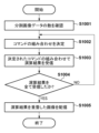
 imaging device 110 are realized, for example, by a processor in the arithmetic processing unit 203 executing a program stored in a memory or the like. However, this is just an example, and part or all of the processing described below may be realized by dedicated hardware. Further, the processing executed by the removable device 100 and the input/output device 130 may also be realized by a processor in each device executing a program stored in a memory or the like, or part or all of the processing may be performed by It may also be realized by dedicated hardware.

(全体の流れ)
図6に、システムで実行される画像解析処理の一連の流れを概略的に示す。本処理では、まず、ユーザによって、撮像装置110に着脱可能デバイス100が装着される(S601)。撮像装置110は、着脱可能デバイス100の初期化シーケンスを実行する(S602)。この初期化シーケンスでは、撮像装置110と着脱可能デバイス100との間で所定のコマンドが送受信されることにより、撮像装置110が、着脱可能デバイス100を使用可能な状態となる。その後、撮像装置110は、着脱可能デバイス100が実行可能な処理を把握し、ローカルで実行可能な(撮像装置110単体で又は撮像装置110と着脱可能デバイス100の組み合わせで実行可能な)処理を把握する(S603)。なお、着脱可能デバイス100は、任意の処理を実行可能なように構成されうるが、撮像装置110側で実行されるべき処理と無関係な処理については考慮されなくてもよい。一例において、撮像装置110は、例えば入出力装置130から事前に取得した実行されうる処理のリストを保持しておいてもよい。この場合、撮像装置110は、着脱可能デバイス100が実行可能な処理を示す情報を着脱可能デバイス100から取得した際に、その処理がリストに含まれているか否かによって、実行されうる処理のみを把握することができる。
(Overall flow)
FIG. 6 schematically shows a series of image analysis processes executed by the system. In this process, first, the user attaches the removable device 100 to the imaging apparatus 110 (S601). The imaging device 110 executes an initialization sequence for the removable device 100 (S602). In this initialization sequence, predetermined commands are exchanged between the imaging apparatus 110 and the removable device 100, so that the imaging apparatus 110 becomes ready to use the removable device 100. After that, the imaging device 110 grasps the processing that can be executed by the removable device 100, and grasps the processing that can be executed locally (that can be executed by the imaging device 110 alone or by a combination of the imaging device 110 and the removable device 100). (S603). Note that although the removable device 100 may be configured to be able to execute arbitrary processing, it is not necessary to consider processing that is unrelated to the processing that should be executed on the imaging device 110 side. In one example, the imaging device 110 may maintain a list of executable processes obtained in advance from the input/output device 130, for example. In this case, when the imaging device 110 acquires information indicating executable processing from the removable device 100, the imaging device 110 selects only the processing that can be executed depending on whether the processing is included in the list. can be grasped.

続いて、撮像装置110は、実行する処理を決定し、必要に応じて着脱可能デバイス100の設定を実行する(S604)。すなわち、実行対象として決定された処理の少なくとも一部が着脱可能デバイス100によって実行される場合に、その処理のための着脱可能デバイス100の設定が実行される。この設定においては、例えば、実行対象の処理に対応する設定データを用いたFPGA402の再構成が行われうる。そして、撮像装置110または着脱可能デバイス100が、解析処理を実行する(S605)。その後、撮像装置110は、後処理を実行する(S606)。なお、S605とS606の処理は繰り返し実行される。図6の処理は、例えば、着脱可能デバイス100が装着された際に実行されるが、例えば着脱可能デバイス100が取り外された際にも、S603の処理が再度実行されるようにするなど、図6の処理の少なくとも一部が繰り返し実行されてもよい。 Subsequently, the imaging apparatus 110 determines the process to be executed, and executes settings of the removable device 100 as necessary (S604). That is, when at least part of the process determined to be executed is to be executed by the removable device 100, the settings of the removable device 100 for the process are executed. In this setting, for example, the FPGA 402 may be reconfigured using setting data corresponding to the process to be executed. Then, the imaging apparatus 110 or the removable device 100 executes analysis processing (S605). After that, the imaging device 110 executes post-processing (S606). Note that the processes of S605 and S606 are repeatedly executed. The process in FIG. 6 is executed, for example, when the removable device 100 is attached, but the process in S603 is executed again when the detachable device 100 is removed, for example. At least a part of the process No. 6 may be repeatedly executed.

S603~S606についてさらに説明する。S603で、撮像装置110の制御部304は、記憶部303に記憶されている、撮像装置110自身の解析部305において実行可能な処理のリストである第1処理リストを読み出す。続いて、制御部304は、デバイス通信部306を制御して、装着された着脱可能デバイス100の特定のアドレスへの読み出し要求(リードコマンド)を発行する。以下では、この特定のアドレスを「アドレスA」と呼ぶ場合がある。なお、アドレスAに格納されているデータの詳細については後述する。制御部304は、アドレスAから読み出したデータに基づいて、着脱可能デバイス100が有する処理機能のリスト(第2処理リスト)を生成する。 S603 to S606 will be further explained. In step S<b>603 , the control unit 304 of the imaging device 110 reads a first processing list, which is a list of processes executable by the analysis unit 305 of the imaging device 110 itself, which is stored in the storage unit 303 . Subsequently, the control unit 304 controls the device communication unit 306 to issue a read request (read command) to a specific address of the attached removable device 100. Below, this specific address may be referred to as "address A." Note that details of the data stored at address A will be described later. Based on the data read from the address A, the control unit 304 generates a list of processing functions that the removable device 100 has (second processing list).

入出力装置130では、撮像装置110から第1処理リストと第2処理リストを、ネットワークを介して取得し、画面表示等によってユーザに提示する。ユーザは、操作部を介して、表示されたリストから実行すべき解析処理(以下では、「実行対象処理」と呼ぶ。)を選択する。入出力装置130は、実行対象処理の選択結果を、撮像装置110へ通知する。 The input/output device 130 acquires the first processing list and the second processing list from the imaging device 110 via the network, and presents them to the user through screen display or the like. The user selects an analysis process to be executed (hereinafter referred to as "execution target process") from the displayed list via the operation unit. The input/output device 130 notifies the imaging device 110 of the selection result of the process to be executed.

S604で、制御部304は、実行対象処理が第2処理リストに含まれる場合、デバイス通信部306を制御して、実行対象処理の設定要求を着脱可能デバイス100に送信する。着脱可能デバイス100の通信部502は、実行対象処理の設定要求を撮像装置110から受信する。通信部502は、撮像装置110から受信した実行対象処理の設定要求を、解析部501に出力する。解析部501は、通信部502から入力された実行対象処理の設定要求に基づいて、着脱可能デバイス100が実行対象処理を実行可能な状態となるようにするための設定を実行する。例えば、処理切替部411が、設定要求に応じて演算処理部412の実行対象処理を切り替える。通信部502は、例えば設定処理が完了した後に、設定完了通知を撮像装置110へ送信する。 In step S<b>604 , if the execution target process is included in the second process list, the control unit 304 controls the device communication unit 306 to transmit a setting request for the execution target process to the removable device 100 . The communication unit 502 of the removable device 100 receives a request for setting a process to be executed from the imaging device 110. The communication unit 502 outputs the execution target process setting request received from the imaging device 110 to the analysis unit 501. The analysis unit 501 performs settings to enable the removable device 100 to execute the execution target process based on the execution target process setting request input from the communication unit 502. For example, the process switching unit 411 switches the execution target process of the arithmetic processing unit 412 in response to a setting request. For example, after the setting process is completed, the communication unit 502 transmits a setting completion notification to the imaging device 110.

S605では、制御部304は、実行対象処理が第2処理リストに含まれている場合、デバイス通信部306を制御して、解析処理対象の画像を着脱可能デバイス100に送信する。例えば、制御部304は、解析処理対象の画像の書き込み要求(ライトコマンド)を発行することにより、着脱可能デバイス100へ解析処理対象の画像を送信する。着脱可能デバイス100の通信部502は、解析処理対象の画像を撮像装置110から受信し、撮像装置110から受信した画像を解析部501に出力する。解析部501は、通信部502から入力された画像に対して、S604で設定された実行対象処理を実行し、記憶部404に格納する。 In S<b>605 , if the execution target process is included in the second process list, the control unit 304 controls the device communication unit 306 to transmit the image to be analyzed to the removable device 100 . For example, the control unit 304 transmits the image to be analyzed to the removable device 100 by issuing a write request (write command) for the image to be analyzed. The communication unit 502 of the detachable device 100 receives an image to be analyzed from the imaging device 110 and outputs the image received from the imaging device 110 to the analysis unit 501. The analysis unit 501 executes the execution target process set in S<b>604 on the image input from the communication unit 502 and stores it in the storage unit 404 .

その後、S606において、通信部502は、撮像装置110からの解析処理結果の読み出し要求(リードコマンド)に応じて、解析部501による処理によって得られた解析処理結果を記憶部404から読み出して、撮像装置110へ送信する。撮像装置110の制御部304は、デバイス通信部306を制御して、着脱可能デバイス100から解析処理結果を受信する。その後、制御部304は、解析部305を制御して、解析処理結果に対して解析後処理を実行する。 After that, in step S606, the communication unit 502 reads the analysis processing result obtained by the processing by the analysis unit 501 from the storage unit 404 in response to a read request (read command) for the analysis processing result from the imaging device 110, and Send to device 110. The control unit 304 of the imaging device 110 controls the device communication unit 306 to receive analysis processing results from the detachable device 100. Thereafter, the control unit 304 controls the analysis unit 305 to perform post-analysis processing on the analysis processing results.

(撮像装置110と着脱可能デバイス100との間の通信)
・着脱可能デバイスのインタフェース構成
ここで、撮像装置110と着脱可能デバイス100との通信について説明する。撮像装置110の演算処理部203と着脱可能デバイス100のSDコントローラ403は、撮像装置110のSD I/F部205のデバイス挿入用ソケットを介し、電源ライン、GNDライン、クロックライン、コマンドライン、データラインで接続される。なお、クロックライン、コマンドライン、及び、データラインは、FPGA402を経由する形で接続されるものとする。クロックラインでは、演算処理部203から出力される同期用のクロックが通信される。コマンドラインでは、演算処理部203からSDコントローラ403への動作要求用に発行するコマンド、コマンドに対するSDコントローラ403から演算処理部203へのレスポンスが通信される。データラインでは、演算処理部203からの書き込みデータ、着脱可能デバイス100からの読み出しデータが通信される。また、演算処理部203は、SD I/F部205のデバイス挿入用ソケットのデバイスディテクト信号のHighとLowを判別することにより、着脱可能デバイス100が挿入されているか否かを認識することができる。
(Communication between imaging device 110 and removable device 100)
- Interface Configuration of Detachable Device Here, communication between the imaging device 110 and the detachable device 100 will be described. The arithmetic processing unit 203 of the imaging device 110 and the SD controller 403 of the removable device 100 connect the power line, GND line, clock line, command line, and data via the device insertion socket of the SD I/F unit 205 of the imaging device 110. connected by a line. Note that the clock line, command line, and data line are connected via the FPGA 402. A synchronization clock output from the arithmetic processing unit 203 is communicated on the clock line. On the command line, a command issued from the arithmetic processing unit 203 to the SD controller 403 to request an operation, and a response from the SD controller 403 to the arithmetic processing unit 203 in response to the command are communicated. Write data from the arithmetic processing unit 203 and read data from the removable device 100 are communicated on the data line. Further, the arithmetic processing unit 203 can recognize whether or not the removable device 100 is inserted by determining whether the device detect signal of the device insertion socket of the SD I/F unit 205 is High or Low. .

・着脱可能デバイスの初期設定
演算処理部203は、SDコントローラ403に対して電源供給後にコマンドライン上でコマンドを発行する。そして、演算処理部203は、SDコントローラ403からのレスポンスと、SDカードとしてのデバイス情報を示す出力データを受信したことに応じて、データの通信用の電圧、通信速度(クロック周波数)等の設定を行う。
- Initial setting of removable device The arithmetic processing unit 203 issues a command on the command line after power is supplied to the SD controller 403. Then, in response to receiving the response from the SD controller 403 and output data indicating device information as an SD card, the arithmetic processing unit 203 sets the voltage for data communication, communication speed (clock frequency), etc. I do.

・コマンドとレスポンスの構成
図7に、コマンドライン上で通信されるコマンドとレスポンスの構成例を示す。これらのコマンドとレスポンスはSD規格に従う構成を有する。演算処理部203からSDコントローラ403に対して発行されるコマンド701は、コマンドナンバー部704と、コマンド引数部705と、誤り訂正用データ部706とを含んで構成される。コマンドナンバー部704には、コマンドの種別を示す値が記述される。例えば、コマンドナンバー部704に値「23」が格納されている場合、そのコマンドがデータブロック数を指定するブロック数指定コマンドであることが示される。また、コマンドナンバー部704に値「25」が格納されている場合、そのコマンドがマルチライトコマンドであることが示され、コマンドナンバー部704に値「12」が格納されている場合、そのコマンドがデータ転送停止コマンドであることが示される。コマンド引数部705では、コマンドの種別に応じて転送データブロック数、メモリの書き込み・読み出しアドレス等の情報が指定される。また、コマンドの最初のビットには、コマンドの開始位置を示すコマンドスタートビット702が付加され、コマンドの最後のビットにはコマンドの終了を示すコマンドエンドビット707が付加される。また、コマンドスタートビット702の後ろに、撮像装置110から着脱可能デバイス100に対して出力された信号であることを示すディレクションビット703も付加される。
- Composition of commands and responses FIG. 7 shows an example of the composition of commands and responses communicated on the command line. These commands and responses have a configuration that complies with the SD standard. The command 701 issued from the arithmetic processing unit 203 to the SD controller 403 includes a command number section 704, a command argument section 705, and an error correction data section 706. A value indicating the type of command is written in the command number section 704. For example, when the value "23" is stored in the command number field 704, it is shown that the command is a block number designation command that designates the number of data blocks. Further, when the value “25” is stored in the command number field 704, it indicates that the command is a multi-write command, and when the value “12” is stored in the command number field 704, the command is This indicates that it is a data transfer stop command. In the command argument section 705, information such as the number of transfer data blocks, memory write/read addresses, etc. is specified depending on the type of command. Further, a command start bit 702 indicating the start position of the command is added to the first bit of the command, and a command end bit 707 indicating the end of the command is added to the last bit of the command. Further, a direction bit 703 indicating that the signal is output from the imaging apparatus 110 to the removable device 100 is added after the command start bit 702 .

演算処理部203からのコマンドに対してSDコントローラ403から返されるレスポンス711は、どのコマンドに対するレスポンスかを示すレスポンスナンバー部714と、レスポンス引数部715と、誤り訂正用データ部716とを含む。また、レスポンスの最初のビットにはレスポンスの開始位置を示すレスポンススタートビット712が付加され、レスポンスの最後のビットにはレスポンスの終了位置を示すレスポンスエンドビット717が付加される。また、レスポンススタートビット712の後ろに着脱可能デバイス100から撮像装置110に対して出力された信号であることを示すディレクションビット713も付加される。レスポンス引数部715には、コマンド種別に応じてSDカードのステータス等の情報が格納される。 A response 711 returned from the SD controller 403 in response to a command from the arithmetic processing unit 203 includes a response number section 714 indicating which command the response is for, a response argument section 715, and an error correction data section 716. Further, a response start bit 712 indicating the start position of the response is added to the first bit of the response, and a response end bit 717 indicating the end position of the response is added to the last bit of the response. Furthermore, a direction bit 713 indicating that the signal is output from the removable device 100 to the imaging device 110 is added after the response start bit 712 . The response argument section 715 stores information such as the status of the SD card depending on the command type.

・データの転送
次に、演算処理部203と着脱可能デバイス100とのデータの送受信の方法を説明する。上述したように、SD I/F部205では、データの書き込み及び読み出し共にブロック単位でデータの転送が行われる。ブロックは、例えば、記憶部404におけるデータの書き込みおよび読みだしの単位であり、例えば512BYTEのサイズを有する。
- Data Transfer Next, a method of transmitting and receiving data between the arithmetic processing unit 203 and the detachable device 100 will be described. As described above, in the SD I/F unit 205, data is transferred in blocks for both data writing and reading. A block is, for example, a unit for writing and reading data in the storage unit 404, and has a size of, for example, 512 BYTE.

演算処理部203が着脱可能デバイス100に対して複数ブロックのデータを転送する方法には以下の3つの方法がある。1つ目の方法は、1ブロック分のデータだけを送信するライトコマンド(以下、シングルライトコマンド)を用いた方法である。シングルライトコマンドは、演算処理部203がブロック指定コマンド、転送停止コマンドを発行せずに、1ブロック分のデータを転送し、書き込みを行うコマンドである。コマンド引数部705には、アクセスする記憶部404のアドレスが設定される。 There are three methods for the arithmetic processing unit 203 to transfer a plurality of blocks of data to the removable device 100 as follows. The first method is a method using a write command (hereinafter referred to as a single write command) that transmits only one block of data. The single write command is a command in which the arithmetic processing unit 203 transfers and writes data for one block without issuing a block designation command or a transfer stop command. The command argument section 705 is set with the address of the storage section 404 to be accessed.

残り2つの方法は、1回のコマンドによって複数ブロック分のデータの転送、書き込みを指示するマルチライトコマンドを用いた方法である。1つ目の方法は、転送データのブロック数指定コマンドによってブロック数が指定された後に、マルチライトコマンドにより、指定されたブロック数だけデータが転送される。ブロック数指定コマンドでは、コマンド引数部705において書き込みデータのブロック数が指定され、マルチライトコマンドでは、コマンド引数部705においてデータが書き込まれるべき記憶部404のアドレスが指定される。2つ目の方法では、ブロック数指定コマンドが発行されることなくマルチライトコマンドが発行されることにより、データ転送が開始され、データ転送が終わった時点で転送停止コマンドが発行されることによって処理が終了する。このとき、マルチライトコマンドのコマンド引数部705において、データが書き込まれるべき記憶部404のアドレスのみが指定される。尚、どちらのマルチライトコマンドによる書き込みにおいても、SDコントローラ403はコマンドで指定されたアドレスから書き込みを開始する。そして、SDコントローラ403は、1ブロック分のデータを入力するごとに書き込みアドレスをインクリメントして記憶部404へのデータの書き込みを行う。演算処理部203は3つの書き込み方法を任意に切り替えることが可能である。 The remaining two methods use a multi-write command that instructs the transfer and writing of multiple blocks of data with a single command. In the first method, the number of blocks is specified by a transfer data block number designation command, and then data is transferred by the specified number of blocks by a multi-write command. In the block number specification command, the number of blocks of write data is specified in the command argument section 705, and in the multi-write command, the address of the storage section 404 to which data is to be written is specified in the command argument section 705. In the second method, data transfer is started by issuing a multi-write command without issuing a block number specification command, and processing is stopped by issuing a transfer stop command when the data transfer is finished. ends. At this time, only the address of the storage unit 404 to which data is to be written is specified in the command argument section 705 of the multi-write command. Note that in writing using either multi-write command, the SD controller 403 starts writing from the address specified by the command. Then, the SD controller 403 increments the write address every time one block of data is input, and writes the data to the storage unit 404. The arithmetic processing unit 203 can arbitrarily switch between three writing methods.

なお、記憶処理が行われる場合、FPGA402は、演算処理部203から送られるコマンドとデータをそのままSDコントローラ403に入力し、SDコントローラ403は、受信したデータをコマンドで指定された記憶部404のアドレスに格納する。画像解析処理が行われる場合には、FPGA402は、演算処理部203から送られるデータに対して解析処理を実行し、その処理結果のデータと、記憶部404の所定のアドレスを指定する情報を、SDコントローラ403に出力する。SDコントローラ403は、指定された記憶部のアドレスに処理結果を格納する。 Note that when storage processing is performed, the FPGA 402 inputs the command and data sent from the arithmetic processing unit 203 as they are to the SD controller 403, and the SD controller 403 stores the received data at the address of the storage unit 404 specified by the command. Store in. When image analysis processing is performed, the FPGA 402 executes analysis processing on data sent from the arithmetic processing unit 203, and stores the processing result data and information specifying a predetermined address in the storage unit 404. Output to SD controller 403. The SD controller 403 stores the processing result at the specified storage unit address.

演算処理部203が着脱可能デバイス100から複数ブロックのデータを読み出す方法は以下の3つの方法がある。1つ目の方法は、1ブロック分のデータだけを読み出し、受信するリードコマンド(以下、シングルリードコマンド)を用いた方法である。シングルリードコマンドは、演算処理部203がブロック指定コマンド、転送停止コマンドを発行せずに、1ブロック分のデータを読み出すコマンドである。コマンド引数部705には、アクセスする記憶部404のアドレスが設定される。 There are three methods for the arithmetic processing unit 203 to read multiple blocks of data from the removable device 100 as follows. The first method uses a read command (hereinafter referred to as a single read command) that reads and receives only one block of data. The single read command is a command in which the arithmetic processing unit 203 reads one block of data without issuing a block designation command or a transfer stop command. The command argument section 705 is set with the address of the storage section 404 to be accessed.

残りの2つの方法は、1回のコマンドで複数ブロックのデータの読み出しを指示する方法である。1つ目の方法では、ブロック数指定コマンドでブロック数が指定されてからマルチリードコマンドを発行することにより、指定されたブロック数のデータが読み出される。ブロック数指定コマンドでは、コマンド引数部705において読み出しデータのブロック数が指定され、マルチリードコマンドのコマンド引数部705においてデータの読み出し元のメモリのアドレスが指定される。2つ目の方法では、ブロック数指定コマンドが発行されることなくマルチリードコマンドが発行されることにより、データの読み出しが開始され、転送停止コマンドが発行されることによって処理が終了する。尚、どちらのマルチリードコマンドによる読み出しにおいても、SDコントローラ403はコマンドで指定されたアドレスから読み出しを開始する。そして、SDコントローラ403は、1ブロック分のデータを出力するごとに読み出しアドレスをインクリメントして記憶部404に格納されているデータを読み出す。演算処理部203は3つの読み出し方法を任意に切り替えることが可能である。 The remaining two methods are methods of instructing reading of multiple blocks of data with a single command. In the first method, the number of blocks is specified with a block number designation command, and then a multi-read command is issued, thereby reading the data of the specified number of blocks. In the block number specification command, the number of blocks of read data is specified in the command argument section 705, and the address of the memory from which the data is read is specified in the command argument section 705 of the multi-read command. In the second method, reading of data is started by issuing a multi-read command without issuing a block number designation command, and processing is ended by issuing a transfer stop command. Note that in reading by either multi-read command, the SD controller 403 starts reading from the address specified by the command. Then, the SD controller 403 increments the read address and reads the data stored in the storage unit 404 every time one block of data is output. The arithmetic processing unit 203 can arbitrarily switch between three reading methods.

なお、書き込みデータ、読み出しデータが1ブロックの場合には、シングルライトコマンド、シングルリードコマンドが発行されることにより、ブロック数指定コマンド、転送停止コマンドが発行されることなく、データの書き込み、読み出しが実行されうる。シングルライトコマンド、シングルリードコマンドにおいても、上述の説明と同様に、コマンド引数部705において、アクセス対象の記憶部404のアドレスが指定される。 Note that if the write data or read data is one block, by issuing a single write command or a single read command, data writing or reading can be performed without issuing a block number designation command or transfer stop command. It can be executed. Also in the single write command and the single read command, the address of the storage unit 404 to be accessed is specified in the command argument section 705, similarly to the above explanation.

演算処理部203は、着脱可能デバイス100に対して書き込みを行うことにより、記憶処理または画像解析処理の対象となるデータを着脱可能デバイス100へ送信することができる。また、演算処理部203は、着脱可能デバイス100に対して読み出しを行うことにより、記憶部404に記憶された画像データ、画像解析処理の処理結果、着脱可能デバイス100が保有する画像解析の処理機能の情報を取得することができる。 By writing to the removable device 100, the arithmetic processing unit 203 can transmit data to be subjected to storage processing or image analysis processing to the removable device 100. In addition, the arithmetic processing unit 203 reads the image data stored in the storage unit 404 from the removable device 100, the processing results of the image analysis process, and the image analysis processing functions possessed by the removable device 100. information can be obtained.

・画像解析処理機能の情報確認
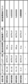
本実施形態の着脱可能デバイス100は、記憶部404の特定のアドレスAに、自装置が有する処理機能の情報を格納する。撮像装置110の演算処理部203は、このアドレスAに対してマルチリードコマンド又はシングルリードコマンドを発行することにより、着脱可能デバイス100が有する処理機能の情報を確認することができる。ここでの処理機能の情報は、処理機能を保有しているか否か、処理が実行された場合に完了するまでの所要時間、処理結果のデータサイズ、処理結果が格納されるアドレス情報を含む。図12に、この処理機能の情報の一例を示す。処理機能保有フラグ1201は、着脱可能デバイス100が画像解析処理機能を有していることを示している。撮像装置110は、処理機能保有フラグ1201を確認することにより、着脱可能デバイス100が画像解析処理機能を有しているか否かを判定する。処理機能分類1202は、着脱可能デバイス100が有している解析処理を示す。入力データサイズ1203及び処理データ数1204は、各々の処理機能のデータの入力仕様に関する情報を示す。また、推定処理時間1205は、データ入力から処理結果出力までに掛かる時間を示し、処理結果データ数1206は処理結果のデータ数を示す。また、処理結果格納アドレス1207は、記憶部404のどこに処理結果が格納されるかを示す。演算処理部203は、図12に示すような記憶部404のアドレスAのデータを読み出すことにより、図13に示すような処理機能テーブルを取得することができる。なお、本明細書においてデータ数とは、データの量(データのサイズ)に対応するブロック数である。
- Confirmation of information on image analysis processing function The removable device 100 of this embodiment stores information on its own processing function at a specific address A in the storage unit 404. By issuing a multi-read command or a single-read command to this address A, the arithmetic processing unit 203 of the imaging device 110 can check information on the processing function that the detachable device 100 has. The processing function information here includes whether the processing function is possessed or not, the time required to complete the process when executed, the data size of the process result, and address information where the process result is stored. FIG. 12 shows an example of information on this processing function. The processing function possession flag 1201 indicates that the removable device 100 has an image analysis processing function. The imaging apparatus 110 determines whether the removable device 100 has an image analysis processing function by checking the processing function possession flag 1201. The processing function classification 1202 indicates the analysis processing that the removable device 100 has. The input data size 1203 and the number of processed data 1204 indicate information regarding the data input specifications of each processing function. Further, the estimated processing time 1205 indicates the time required from data input to processing result output, and the processing result data number 1206 indicates the number of processing result data. Further, the processing result storage address 1207 indicates where in the storage unit 404 the processing result is stored. The arithmetic processing unit 203 can obtain a processing function table as shown in FIG. 13 by reading the data at address A of the storage unit 404 as shown in FIG. Note that in this specification, the number of data refers to the number of blocks corresponding to the amount of data (size of data).

また、着脱可能デバイス100は、演算処理部203からアドレスAに対するリードコマンドが発行されない場合には、自装置が装着された機器が画像解析処理機能を使用しない機器であると判断する。この場合、着脱可能デバイス100は、転送されるデータに関しては記憶部404に対する記憶処理のみを実行するようにしうる。これにより、着脱可能デバイス100は、画像解析処理機能を必要としない機器に対しては、メモリデバイスとしてのみ機能することが可能となる。ここでは、記憶部404の特定のアドレスAに処理機能の情報を格納しておく方法を示したが、これに限定されない。例えば、着脱可能デバイス100の初期設定時に使用されるコマンドに対するレスポンスにおける、レスポンス引数部715に、処理機能の情報を付加するようにしてもよい。 Further, if the read command for address A is not issued from the arithmetic processing unit 203, the removable device 100 determines that the device to which it is attached is a device that does not use the image analysis processing function. In this case, the removable device 100 may perform only storage processing on the storage unit 404 regarding the data to be transferred. This allows the removable device 100 to function only as a memory device for equipment that does not require an image analysis processing function. Although a method of storing processing function information at a specific address A of the storage unit 404 has been described here, the present invention is not limited to this. For example, information about the processing function may be added to the response argument section 715 in a response to a command used when initializing the removable device 100.

なお、撮像装置110は、例えば、着脱可能デバイス100の初期化設定終了後に、記憶部404のアドレスAの読み出しを実行する。また、撮像装置110は、ソケットにおいてデバイスのディテクトがされなくなった場合に、読み込んだ情報を破棄する。撮像装置110は、情報の破棄の後にデバイスがソケットに挿入された場合、初期化設定終了後に再度アドレスAの値を読み出す。これにより、撮像装置110は、異なる着脱可能デバイスが挿入された場合に、その着脱可能デバイスの保有機能の情報を読み出し、設定することができる。 Note that, for example, the imaging apparatus 110 executes reading of the address A of the storage unit 404 after completing the initialization settings of the removable device 100. Further, the imaging device 110 discards the read information when a device is no longer detected in the socket. When the device is inserted into the socket after the information is discarded, the imaging device 110 reads the value of address A again after completing the initialization settings. Thereby, when a different removable device is inserted, the imaging apparatus 110 can read and set information on the functions possessed by the removable device.

<画像データの生成方法>
図8を用いて、顔認証システムの場合を例に、本実施形態の撮像装置110が、画像を分割して画像データを生成する方法を説明する。したがって、以下の例では、着脱可能デバイス100の演算処理部412が、入力された画像から顔認証を行うための推論演算処理を行う。
<How to generate image data>
Using FIG. 8 as an example of a face authentication system, a method in which the imaging device 110 of this embodiment divides an image to generate image data will be described. Therefore, in the following example, the calculation processing unit 412 of the removable device 100 performs inference calculation processing for performing face authentication from the input image.

画像800は、演算処理部203が画像処理部202から受け取った画像である。学習画像803は、演算処理部412で行われる推論演算処理の学習に用いられた画像であり、ある一定の画像サイズを有し、その画像内で顔が一定の割合を占めるように調整されている。そのため、演算処理部412で行われる推論演算処理には、学習画像803の画像サイズと画像内に占める顔の大きさの割合にできるだけ近い画像データが入力されることが望ましい。 The image 800 is an image that the arithmetic processing unit 203 receives from the image processing unit 202. The learning image 803 is an image used for learning the inference calculation process performed by the calculation processing unit 412, has a certain image size, and is adjusted so that the face occupies a certain proportion in the image. There is. Therefore, it is desirable that image data that is as close as possible to the ratio between the image size of the learning image 803 and the size of the face in the image be input to the inference calculation process performed by the calculation processing unit 412.

そこで、演算処理部203は、被写体距離の違いによって被写体801と被写体802が画像800のように撮影された場合、被写体801と被写体802の画像上の位置に従って、学習画像803の比率に近くなるように画像を分割する。図6の画像800において示されている破線は、画像800の分割の一例を示している。加えて、演算処理部203は学習画像803の画像サイズに合うように伸縮処理を行い、着脱可能デバイス100への送信対象となる複数の分割画像データを生成する。結果、複数の分割画像データの大きさはすべて等しい。なお、演算処理部203が分割位置を画像800から判断して設定するようにしたが、入出力装置130からユーザが直接設定するようにしてもよい。 Therefore, when the subject 801 and the subject 802 are photographed as in the image 800 due to the difference in subject distance, the arithmetic processing unit 203 adjusts the ratio so that the ratio approaches the learning image 803 according to the positions of the subject 801 and the subject 802 on the image. Split the image into. The broken lines shown in the image 800 in FIG. 6 indicate an example of division of the image 800. In addition, the arithmetic processing unit 203 performs expansion/contraction processing to match the image size of the learning image 803, and generates a plurality of divided image data to be transmitted to the detachable device 100. As a result, the sizes of the plurality of divided image data are all equal. Note that although the arithmetic processing unit 203 determines and sets the division position from the image 800, the user may directly set the division position from the input/output device 130.

<画像データの送信処理>
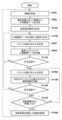
図9を用いて、撮像装置(演算処理部203)が、撮像部201により撮像された画像を分割して送信する処理を説明する。なお、図9に示される処理は、図6のS604からS605の間に、演算処理部203により行われる処理である。
<Image data transmission processing>
A process in which the imaging device (arithmetic processing unit 203) divides and transmits an image captured by the imaging unit 201 will be described using FIG. 9 . Note that the processing shown in FIG. 9 is processing performed by the arithmetic processing unit 203 between S604 and S605 in FIG.

S901において、撮像装置110の撮像部201が画像を取得すると、画像処理部202がその取得された画像に対して画像処理を行う。演算処理部203は、画像処理部202により画像処理が施された画像を取得する。S902において、演算処理部203は、S204で設定された解析処理に応じて、図8の参照により上述した方法で、複数の分割画像データを生成する。 In S901, when the imaging unit 201 of the imaging device 110 acquires an image, the image processing unit 202 performs image processing on the acquired image. The arithmetic processing unit 203 acquires the image that has been subjected to image processing by the image processing unit 202. In S902, the arithmetic processing unit 203 generates a plurality of divided image data according to the analysis processing set in S204 using the method described above with reference to FIG.

S903において、演算処理部203は、1つの分割画像データについてどのようなコマンドの組み合わせでその分割画像データを送信するかを決定する。以下、決定されたコマンドの組み合わせをコマンド群という。着脱可能デバイス100上で実行される推論演算処理に必要な時間は、入力される画像データのサイズや、演算処理部412の動作周波数、つまり、着脱可能デバイス100との通信速度に比例して大きくなる。一方で、画像解析処理全体として必要となる処理速度に応じて、演算処理部412の演算時間として割り当てられる時間の上限がある。そのため、この上限時間を満たす範囲で、コマンドの組み合わせが選択され、分割画像データの送信に用いられるコマンド群が決定される。例えば、分割画像データのデータ量とコマンドの通信に要する時間に基づいて、要求された時間内に分割画像データの送信を終えるようにコマンド群を構成するコマンドの組み合わせが決定される。ただし、データ転送の方法が変わる際には、シングルライトコマンド、もしくは、マルチライトコマンドを発行する必要があるので、このようなコマンドの送信にかかる時間も加味する必要がある。例えば、シングルライトコマンドは、1ブロックごとにコマンドの通信が発生するので送信に時間を要する。従って、マルチライトコマンドとデータ転送停止コマンドを用いたデータ送信は、シングルライトコマンドに比べて高速である。 In S903, the arithmetic processing unit 203 determines what combination of commands should be used to transmit one piece of divided image data. Hereinafter, the determined combination of commands will be referred to as a command group. The time required for the inference calculation process executed on the removable device 100 increases in proportion to the size of input image data and the operating frequency of the calculation processing unit 412, that is, the communication speed with the removable device 100. Become. On the other hand, there is an upper limit to the time that can be allocated as the calculation time of the calculation processing unit 412, depending on the processing speed required for the entire image analysis process. Therefore, a combination of commands is selected within a range that satisfies this upper limit time, and a group of commands to be used for transmitting the divided image data is determined. For example, a combination of commands forming a command group is determined based on the data amount of the divided image data and the time required for communicating the commands so that the transmission of the divided image data is completed within the requested time. However, when changing the data transfer method, it is necessary to issue a single write command or a multi-write command, so the time required to send such a command must also be taken into account. For example, a single write command requires time to transmit because command communication occurs for each block. Therefore, data transmission using a multi-write command and a data transfer stop command is faster than a single write command.

S904では、演算処理部203が、S903で決定されたコマンド群(コマンドの組み合わせ)に従って、着脱可能デバイス100に対して、ライトコマンドまたはマルチライトコマンドを用いて分割画像データの送信を複数回実行する。S905において、演算処理部203は、取得された画像から生成された複数の分割画像データの全てを送信し終えたたかどうかを判定する。全ての分割画像データを送信済みと判定された場合は、本処理を終了する。未送信の分割画像データが存在する場合は、演算処理部203は、次の分割画像データを選択し、処理をS903へ戻す。ただし、演算処理部203は、送信に用いたコマンドの組み合わせを記憶しておき、次のS903では記憶しておいたコマンドの組み合わせと一致しないようにコマンドの組み合わせを選択または決定する。こうして、複数の分割画像データが送信される間に、送信に用いられるコマンド群を構成するコマンドの組み合わせが変更される。 In S904, the arithmetic processing unit 203 transmits divided image data multiple times using a write command or a multi-write command to the removable device 100 according to the command group (combination of commands) determined in S903. . In S905, the arithmetic processing unit 203 determines whether all of the plurality of divided image data generated from the acquired image has been transmitted. If it is determined that all the divided image data has been transmitted, this process ends. If there is unsent divided image data, the arithmetic processing unit 203 selects the next divided image data and returns the process to S903. However, the arithmetic processing unit 203 stores the combination of commands used for transmission, and in the next step S903 selects or determines a combination of commands so that it does not match the stored combination of commands. In this way, while a plurality of pieces of divided image data are being transmitted, the combination of commands forming the command group used for transmission is changed.

なお、上述した上限時間を満足する複数のコマンド群(複数種類のコマンドの組み合わせ)をリストとして登録しておき、順番に選択するようにしてもよい。なお、リストに登録されているすべての組み合わせについて選択を終えた後、選択の順番を変更するようにしてもよい。また、図8で説明したように、各々の分割画像データのサイズは所定サイズに揃えられるので、着脱可能デバイス100の演算処理部412は、送信されたデータのサイズが所定サイズに到達したことにより、1つの分割画像データが送信されたことを把握できる。なお、分割画像データごとに、その開始および/または終了を示す所定コードが送信され、演算処理部412がその所定コードを検出することで分割画像データの送信を把握するようにしてもよい。この場合、複数の分割画像データのサイズはそれぞれ異なっていてもよい。 Note that a plurality of command groups (combinations of a plurality of types of commands) that satisfy the above-mentioned upper limit time may be registered as a list and selected in order. Note that the selection order may be changed after all combinations registered in the list have been selected. Further, as explained in FIG. 8, the size of each divided image data is adjusted to a predetermined size, so that when the size of the transmitted data reaches the predetermined size, the arithmetic processing unit 412 of the removable device 100 , it can be recognized that one piece of divided image data has been transmitted. Note that a predetermined code indicating the start and/or end of each piece of divided image data may be transmitted, and the arithmetic processing unit 412 may detect the predetermined code to detect the transmission of the divided image data. In this case, the sizes of the plurality of divided image data may be different from each other.

<演算結果の受信処理>
次に、撮像装置110が着脱可能デバイス100から演算結果を受信する場合の処理を説明する。演算処理部203は、シングルリードコマンド、マルチリードコマンドを用いて、着脱可能デバイス100からFPGA402(演算処理部412)による演算結果を受信する。シングルリードコマンド、マルチリードコマンドは上述の通りである。
<Receiving processing of calculation results>
Next, a process when the imaging device 110 receives a calculation result from the detachable device 100 will be described. The arithmetic processing unit 203 receives a calculation result by the FPGA 402 (arithmetic processing unit 412) from the removable device 100 using a single read command and a multi-read command. The single read command and multi-read command are as described above.

図10は、演算処理部203が着脱可能デバイス100で推論処理された演算結果を受信する処理を示すフローチャートである。図10のフローチャートに示される処理の開始時には、図9により上述した処理が終了し、着脱可能デバイス100において全ての分割画像データに対して演算処理部412による推論処理が行われ、記憶部404に演算結果が格納されている。 FIG. 10 is a flowchart showing a process in which the arithmetic processing unit 203 receives the arithmetic result subjected to inference processing by the detachable device 100. At the start of the process shown in the flowchart of FIG. 10, the process described above in FIG. The calculation results are stored.

S1001において、演算処理部203は、S902で生成された分割画像データの数を確認する。演算処理部203は、取得した分割画像データの数を、読み出すべき演算結果の数としてセットする。S1002~S1004では、演算結果を所定量ずつ読み出す読出処理が繰り返される。本例では、所定量の演算結果とは、1つの分割画像データに対する演算結果である。S1002において、演算処理部203は、どのようなコマンドの組み合わせで演算結果を受信するかを決定する。以下、このようなコマンドの組み合わせを、図9の説明と同様に、コマンド群とも称する。コマンドの組み合わせの決め方は、S903と同様の考え方となるが、受信処理におけるコマンド群はリードコマンド、および/または、マルチリードコマンドにより構成される。こうして、演算結果を所定量ずつ受信するにおいて、その所定量とコマンドの通信に要する時間に基づいて、要求された時間内に所定量のデータの受信を終えるようにコマンド群が構成される。 In S1001, the arithmetic processing unit 203 checks the number of divided image data generated in S902. The calculation processing unit 203 sets the number of acquired divided image data as the number of calculation results to be read out. In S1002 to S1004, a read process of reading out a predetermined amount of calculation results is repeated. In this example, the predetermined amount of calculation results is the calculation result for one piece of divided image data. In S1002, the calculation processing unit 203 determines what combination of commands should be used to receive the calculation results. Hereinafter, such a combination of commands will also be referred to as a command group, similar to the description of FIG. The method of determining the combination of commands is similar to that in S903, but the command group in the reception process is composed of read commands and/or multi-read commands. In this way, when receiving a predetermined amount of calculation results, a command group is configured based on the predetermined amount and the time required for communication of the command so that the reception of the predetermined amount of data is completed within the requested time.

S1003では、演算処理部203が、S1002で決定されたコマンド群(コマンドの組み合わせ)を用いて、着脱可能デバイス100から演算結果の読み出しを複数回実行し、それらを受信する。S1004では、演算処理部203が、S1001でセットされた演算結果の数と読み出した演算結果の合計数を比較する。両者が一致した場合は演算結果が全て読み出されたと判断され、処理は画像の後処理を行うためにS1005へ移行する。不一致の場合には未受信の演算結果があると判断され、残りの演算結果を読み出すために、処理はS1002へ移行する。なお、演算処理部203は受信に使用したコマンドの組み合わせを記憶しておき、次のS1002では記憶しておいたコマンドの組み合わせと一致しないようにコマンドの組み合わせを選択する。こうして、演算結果が送信される間に、送信に用いられるコマンド群を構成するコマンドの組み合わせが変更される。 In S1003, the calculation processing unit 203 uses the command group (combination of commands) determined in S1002 to execute reading of calculation results from the removable device 100 multiple times, and receives them. In S1004, the calculation processing unit 203 compares the number of calculation results set in S1001 with the total number of read calculation results. If the two match, it is determined that all the calculation results have been read out, and the process moves to S1005 to perform post-processing of the image. If they do not match, it is determined that there are unreceived calculation results, and the process moves to S1002 to read the remaining calculation results. Note that the arithmetic processing unit 203 stores the combination of commands used for reception, and in the next step S1002 selects a combination of commands so that it does not match the stored combination of commands. In this way, while the calculation results are being transmitted, the combination of commands that make up the command group used for transmission is changed.

撮像装置110は、分割画像データの送信順を把握しており、S1003で受信された演算結果がどの分割画像データに対応するものであるかを判定することができる。したがって、S1005では、演算処理部203が、上述のS1001~S1004の処理で取得した演算結果を元の画像に重畳し、配信部204からネットワーク120へ配信する。 The imaging device 110 knows the transmission order of the divided image data, and can determine which divided image data the calculation result received in S1003 corresponds to. Therefore, in S1005, the calculation processing unit 203 superimposes the calculation results obtained in the processes of S1001 to S1004 described above on the original image, and distributes the superimposed image to the network 120 from the distribution unit 204.

以上のように第1実施形態では、撮像装置110は、画像データを分割することで得られた複数の分割画像データを着脱可能デバイス100に送信し、着脱可能デバイス100の演算処理部412に演算処理を行わせる。このとき、複数の分割画像データを送信するために複数種類のライトコマンドの組み合わせを用いるとともに、分割画像データごとにその組み合わせを異ならせている。したがって、分割画像データの区切りを示すための所定のコード、演算処理の対象となる分割画像データのサイズなどを知らない第3者には、撮像装置110により着脱可能デバイス100へ書き込まれた画像を判別することが困難である。また、本実施形態では、演算結果を取得する際にも、演算結果ごとに異なるリードコマンドの組み合わせが用いられる。したがって、演算結果のデータサイズなどが分かりにくくなり、第3者が撮像装置110により読み出された演算結果の内容を特定されてしまう可能性を低減することができる。 As described above, in the first embodiment, the imaging device 110 transmits a plurality of divided image data obtained by dividing image data to the removable device 100, and causes the arithmetic processing unit 412 of the removable device 100 to perform calculations. Let the process take place. At this time, combinations of multiple types of write commands are used to transmit the plurality of divided image data, and the combinations are different for each divided image data. Therefore, a third party who does not know the predetermined code indicating the division of divided image data, the size of the divided image data to be subjected to arithmetic processing, etc., cannot read the image written to the removable device 100 by the imaging device 110. Difficult to distinguish. Furthermore, in the present embodiment, when acquiring calculation results, a different combination of read commands is used for each calculation result. Therefore, it becomes difficult to understand the data size of the calculation result, and it is possible to reduce the possibility that a third party will identify the contents of the calculation result read by the imaging device 110.

<第2実施形態>
第2実施形態では、複数のフレームに渡って、第1実施形態に示す分割画像データの送信処理、演算結果の受信処理と、を組み合わせた場合の、撮像装置110と着脱可能デバイス100の送受信フローとその効果を説明する。尚、第1実施形態で示した構成と、画像の送信、演算結果の受信単体の制御方法、フローは、第2実施形態においても同様である。
<Second embodiment>
In the second embodiment, the transmission and reception flow between the imaging apparatus 110 and the removable device 100 is described when the processing for transmitting divided image data and the processing for receiving calculation results shown in the first embodiment are combined over a plurality of frames. and its effects. The configuration shown in the first embodiment, and the control method and flow for transmitting images and receiving calculation results are the same in the second embodiment.

<フレーム間の送受信処理>
図11は、第2実施形態による撮像装置110の送受信動作を説明するフローチャートである。以下、図11のフローチャートを用いて、撮像装置110と着脱可能デバイス100の複数フレームに渡る送受信処理を説明する。尚、第1実施形態と同じ符号で示す処理については、同様の処理を行うものとする。図11に示すフローチャートは、図6に示すS604からS606の間に行われる処理である。なお、図11に示される処理では、演算処理の対象である画像(分割画像データ)を送信する処理から開始される。
<Transmission/reception processing between frames>
FIG. 11 is a flowchart illustrating the transmission and reception operations of the imaging device 110 according to the second embodiment. The transmission and reception processing of multiple frames between the imaging apparatus 110 and the removable device 100 will be described below using the flowchart of FIG. Note that processes indicated by the same reference numerals as in the first embodiment are performed in the same manner. The flowchart shown in FIG. 11 is the process performed between S604 and S606 shown in FIG. 6. Note that the process shown in FIG. 11 starts with a process of transmitting an image (divided image data) that is a target of arithmetic processing.

S1101において、演算処理部203は、送信と受信の順序を決める。着脱可能デバイス100は、演算結果のデータをFPGA402内部、もしくは、記憶部404に保存することができる。そのため、必ずしも分割画像データの送信と、演算結果の受信をセットで行う必要はない。なお、送信と受信の順序の決定においては、それまでの送信処理により送信された分割画像データに関して未受信の演算結果が記憶部404に存在している状態で受信処理が実行されるように考慮される。 In S1101, the arithmetic processing unit 203 determines the order of transmission and reception. The removable device 100 can store the data of the calculation results inside the FPGA 402 or in the storage unit 404. Therefore, it is not necessarily necessary to transmit the divided image data and receive the calculation results as a set. Note that in determining the order of transmission and reception, consideration is given so that the reception process is executed in a state where unreceived calculation results exist in the storage unit 404 regarding the divided image data transmitted in the previous transmission process. be done.

S1102において、演算処理部203は、画像を分割して得られた複数の分割画像データをどのような順序で送信するかを決定し、決定された順序に基づいて次に送信される分割画像データを特定する。なお、演算処理部203は、S1102で決定された送信の順序の情報をS1005まで保持しておく。そして、演算処理部203は、分割画像データを送信するためのコマンド群を決定し(S903)、決定されたコマンド群を用いてS1102で送信対象に決定された分割画像データを送信する(S904)。S1103において、演算処理部203は、S1101で決定された送受信の順序を確認し、次の処理が送信処理であるか受信処理であるかを判断する。次の処理が送信処理の場合、処理はS1102へ移行する。一方、次の処理が受信処理の場合、処理はS1002へ移行する。 In S1102, the arithmetic processing unit 203 determines the order in which to transmit the plurality of divided image data obtained by dividing the image, and selects the divided image data to be transmitted next based on the determined order. Identify. Note that the arithmetic processing unit 203 retains information on the transmission order determined in S1102 until S1005. The arithmetic processing unit 203 then determines a command group for transmitting the divided image data (S903), and uses the determined command group to transmit the divided image data determined to be the transmission target in S1102 (S904). . In S1103, the arithmetic processing unit 203 checks the order of transmission and reception determined in S1101, and determines whether the next process is a transmission process or a reception process. If the next process is a transmission process, the process moves to S1102. On the other hand, if the next process is a reception process, the process moves to S1002.

演算処理部203は、S1002においてコマンド群を構成するリードコマンドの組み合わせを決定する。S1104において、演算処理部203は、S1002で決定したコマンド群(リードコマンドの組み合わせ)を用いて、着脱可能デバイス100から演算結果を受信する。演算結果は、S1102で決定された順序(分割画像データの送信順序)で受信されることになる。演算処理部203は、S1102で決定された、分割画像データの送信の順序の情報を保持しており、この情報から、順次に受信される演算結果がどの分割画像データに対する演算結果であるかを判断できる。 The arithmetic processing unit 203 determines a combination of read commands forming a command group in S1002. In S1104, the calculation processing unit 203 receives the calculation result from the removable device 100 using the command group (combination of read commands) determined in S1002. The calculation results are received in the order determined in S1102 (the order in which the divided image data is transmitted). The calculation processing unit 203 holds information on the transmission order of the divided image data determined in S1102, and uses this information to determine which divided image data the calculation results that are sequentially received correspond to. I can judge.

S1105において、演算処理部203は、S1101で決めた送受信の順序を確認し、次の処理が送信処理であるか受信処理であるかを判断する。次の処理が送信処理の場合は、処理はS1102へ移行する。一方、次のコマンドが受信処理の場合は、処理はS1004へ移行する。S1004において、演算処理部203は、全ての演算結果を受信し終えたか否か(例えば、S902で生成した分割画像データの数と一致する演算結果を受信したか否か)を判断する。演算結果を受信し終えていなければ処理はS1002に戻り、演算処理部203は、次の演算結果の読み出しを行う。 In S1105, the arithmetic processing unit 203 checks the order of transmission and reception determined in S1101, and determines whether the next process is a transmission process or a reception process. If the next process is a transmission process, the process moves to S1102. On the other hand, if the next command is reception processing, the process moves to S1004. In S1004, the calculation processing unit 203 determines whether all calculation results have been received (for example, whether calculation results that match the number of divided image data generated in S902 have been received). If the calculation results have not been received yet, the process returns to S1002, and the calculation processing unit 203 reads the next calculation result.

S1004において、全ての演算結果の受信を終えたと判断された場合、処理はS1005へ進む。S1005において、演算処理部203は、S1102で決定された分割画像データの送信の順序を参照して、読み出された演算結果を複数の分割画像データの各々に対応付ける。こうして、演算処理部203は、S901で取得された画像に演算結果を適切に重畳して配信することができる。S1005で演算結果を重畳した画像が配信された後、処理は、S901へ戻り、次のフレームの画像に対して同様の処理が行われる。ただし、演算処理部203は、前回のフレームにおいて決定された送受信の順序と分割画像データの送信の順序を記憶しておく。そして、新たなフレームの画像について処理を行う場合には、S1101とS1102において、演算処理部203は、記憶しておいた順序と一致しないように、送受信の順序と分割画像データの送信の順序を決定する。 If it is determined in S1004 that all calculation results have been received, the process advances to S1005. In S1005, the calculation processing unit 203 refers to the transmission order of the divided image data determined in S1102 and associates the read calculation result with each of the plurality of divided image data. In this way, the calculation processing unit 203 can appropriately superimpose the calculation result on the image acquired in S901 and distribute it. After the image on which the calculation results are superimposed is distributed in S1005, the process returns to S901, and the same process is performed on the image of the next frame. However, the arithmetic processing unit 203 stores the transmission/reception order and the transmission order of divided image data determined in the previous frame. When processing a new frame image, in S1101 and S1102, the arithmetic processing unit 203 changes the order of transmission and reception and the order of transmission of divided image data so that the order does not match the stored order. decide.

以上のように、第2実施形態によれば、ライトコマンドの組み合わせ、リードコマンドの組み合わせ、画像データの送信動作と演算結果の読み出し動作の順番、着脱可能デバイス100へ送信される分割画像データの位置の順序が変更される。従って、これらを把握していない第3者は、たとえ通信プロトコルが既知であっても、撮像装置110と着脱可能デバイス100の間のデータの送受信に関して、その内容を把握することが困難である。 As described above, according to the second embodiment, the combination of write commands, the combination of read commands, the order of image data transmission operation and operation result readout operation, and the position of divided image data transmitted to removable device 100 The order of is changed. Therefore, even if the communication protocol is known, it is difficult for a third party who does not know these things to understand the contents of data transmission and reception between the imaging device 110 and the detachable device 100.

なお、第2実施形態では、コマンドの組み合わせと分割画像データの送信の順序を変更したが、分割画像データの送信の順序を変更するだけでも、送信内容についての第3者による解析されてしまう可能性を低減することができる。また、第1実施形態、第2実施形態では、着脱可能デバイス100を装着する電子機器として撮像装置を例示したが、これに限られるものではない。また、上記実施形態では、画像データを分割して得られた複数の分割画像データを着脱可能デバイス100へ送信される分割データとして説明したが、これに限られるものではない。すなわち、演算処理の対象となるデータから演算処理の処理単位に対応した複数の分割データを取得し、これを送信する構成であればよく、データの内容は何等限定されるものではない。 In addition, in the second embodiment, the combination of commands and the order of sending divided image data are changed, but even if the order of sending divided image data is simply changed, the transmitted content may be analyzed by a third party. It is possible to reduce the Further, in the first embodiment and the second embodiment, an imaging device is illustrated as an electronic device to which the detachable device 100 is attached, but the present invention is not limited to this. Further, in the above embodiment, a plurality of divided image data obtained by dividing image data is described as divided data to be transmitted to the removable device 100, but the present invention is not limited to this. In other words, the configuration may be such that a plurality of divided data corresponding to the processing unit of the arithmetic processing are obtained from the data to be subjected to the arithmetic processing and transmitted, and the content of the data is not limited in any way.

(その他の実施形態)
本発明は、上述の実施形態の1以上の機能を実現するプログラムを、ネットワーク又は記憶媒体を介してシステム又は装置に供給し、そのシステム又は装置のコンピュータにおける1つ以上のプロセッサーがプログラムを読出し実行する処理でも実現可能である。また、1以上の機能を実現する回路(例えば、ASIC)によっても実現可能である。
(Other embodiments)
The present invention provides a system or device with a program that implements one or more of the functions of the embodiments described above via a network or a storage medium, and one or more processors in the computer of the system or device reads and executes the program. This can also be achieved by processing. It can also be realized by a circuit (for example, ASIC) that realizes one or more functions.

本発明は上記実施の形態に制限されるものではなく、本発明の精神及び範囲から離脱することなく、様々な変更及び変形が可能である。従って、本発明の範囲を公にするために、以下の請求項を添付する。 The present invention is not limited to the above-described embodiments, and various changes and modifications can be made without departing from the spirit and scope of the present invention. Therefore, to set out the scope of the invention, the following claims are hereby appended.

100a~100d:着脱可能デバイス、110a~110d:撮像装置、120:ネットワーク、130:入出力装置、201:撮像部、202:画像処理部、203:演算処理部、204:配信部、205:SD I/F部、301:撮像制御部、302:信号処理部、303:記憶部、304:制御部、305:解析部、306:デバイス通信部、307:ネットワーク通信部、401:I/F部、402:FPGA、403:SDコントローラ、404:記憶部、501:解析部、502:通信部 100a to 100d: detachable device, 110a to 110d: imaging device, 120: network, 130: input/output device, 201: imaging section, 202: image processing section, 203: arithmetic processing section, 204: distribution section, 205: SD I/F section, 301: Imaging control section, 302: Signal processing section, 303: Storage section, 304: Control section, 305: Analysis section, 306: Device communication section, 307: Network communication section, 401: I/F section , 402: FPGA, 403: SD controller, 404: Storage section, 501: Analysis section, 502: Communication section

Claims (19)

演算処理部を備えたデバイスを着脱可能な電子機器であって、
前記演算処理部の処理対象であるデータを分割して複数の分割データを得る分割手段と、
前記複数の分割データの各々を前記デバイスへ送信するための、複数種類のコマンドの組み合わせである第1のコマンド群を決定する決定手段と、
前記決定手段により決定された前記第1のコマンド群を用いて分割データを送信する送信手段と、を備え、
前記決定手段は、前記複数の分割データの内のある分割データを送信する場合と、他の分割データを送信する場合とで、前記第1のコマンド群を構成するコマンドの組み合わせを変更することを特徴とする電子機器。
An electronic device to which a device equipped with an arithmetic processing unit can be attached and detached,
dividing means for dividing the data to be processed by the arithmetic processing unit to obtain a plurality of divided data;
determining means for determining a first command group that is a combination of multiple types of commands for transmitting each of the plurality of divided data to the device;
transmitting means for transmitting divided data using the first command group determined by the determining means,
The determining means may change the combination of commands forming the first command group depending on when transmitting a certain divided data among the plurality of divided data and when transmitting other divided data. Featured electronic equipment.
前記分割データは、前記演算処理部の処理単位に対応していることを特徴とする請求項1に記載の電子機器。 The electronic device according to claim 1, wherein the divided data corresponds to a processing unit of the arithmetic processing unit. 前記複数の分割データのサイズが同じであることを特徴とする請求項2に記載の電子機器。 The electronic device according to claim 2, wherein the plurality of divided data have the same size. 前記データは画像データであり、
前記分割手段は、
前記画像データにおける被写体の大きさと位置に基づいて前記画像データを複数種類の大きさの画像へ分割して複数の分割画像を生成し、
前記複数の分割画像の大きさを所定の大きさに揃えることにより得られる複数の分割画像データを、前記複数の分割データとして得ることを特徴とする請求項3に記載の電子機器。
The data is image data,
The dividing means is
dividing the image data into images of a plurality of types of sizes based on the size and position of the subject in the image data to generate a plurality of divided images;
4. The electronic device according to claim 3, wherein a plurality of divided image data obtained by aligning the sizes of the plurality of divided images to predetermined sizes is obtained as the plurality of divided data.
前記分割手段は、前記複数の分割データの各々に、データの開始または終了を示す情報を付加することを特徴とする請求項2に記載の電子機器。 3. The electronic device according to claim 2, wherein the dividing means adds information indicating the start or end of data to each of the plurality of divided data. 前記決定手段は、所定の通信規格に準拠した複数種類のコマンドを組み合わせることにより前記第1のコマンド群を決定することを特徴とする請求項1乃至5のいずれか1項に記載の電子機器。 6. The electronic device according to claim 1, wherein the determining means determines the first command group by combining a plurality of types of commands compliant with a predetermined communication standard. 前記決定手段は、前記分割データのデータ量とコマンドの通信に要する時間に基づいて、要求された時間内に前記分割データの送信を終えるように前記第1のコマンド群を構成するコマンドの組み合わせを決定することを特徴とする請求項1乃至6のいずれか1項に記載の電子機器。 The determining means selects a combination of commands constituting the first command group based on the data amount of the divided data and the time required for communication of the commands so that the transmission of the divided data is completed within a requested time. The electronic device according to any one of claims 1 to 6, characterized in that the electronic device determines. 前記処理対象として複数のデータを送信する場合に、データごとに、前記送信手段による前記複数の分割データの送信の順序を変更する変更手段を更に備えることを特徴とする請求項1乃至7のいずれか1項に記載の電子機器。 8. Any one of claims 1 to 7, further comprising a changing unit that changes the order of transmission of the plurality of divided data by the transmitting unit for each data when transmitting a plurality of data as the processing target. The electronic device according to item 1. 前記変更手段により変更された送信の順序を保持する保持手段をさらに備えることを特徴とする請求項8に記載の電子機器。 The electronic device according to claim 8, further comprising a holding unit that holds the transmission order changed by the changing unit. 前記演算処理部による演算結果を前記デバイスから読み出す読出手段をさらに備えることを特徴とする請求項1乃至7のいずれか1項に記載の電子機器。 The electronic device according to any one of claims 1 to 7, further comprising reading means for reading out a calculation result by the calculation processing section from the device. 前記処理対象として複数のデータを送信する場合に、データごとに、前記送信手段による前記複数の分割データの送信の順序を変更する変更手段と、
前記変更手段により変更された送信の順序を保持する保持手段と、を備え、
前記読出手段により読み出された演算結果が、前記保持手段に保持されている送信の順序に基づいて前記複数の分割データの各々に対応付けられることを特徴とする請求項10に記載の電子機器。
changing means for changing the order of transmission of the plurality of divided data by the transmitting means for each data when transmitting a plurality of data as the processing target;
holding means for holding the transmission order changed by the changing means,
11. The electronic device according to claim 10, wherein the calculation result read by the reading means is associated with each of the plurality of divided data based on a transmission order held in the holding means. .
前記読出手段は、
所定量のデータを読み出すための複数種類のコマンドの組み合わせである第2のコマンド群を決定し、
前記第2のコマンド群を用いて前記演算結果を前記所定量ずつ前記デバイスから読み出し、
前記所定量の演算結果を読み出す間に、前記第2のコマンド群を構成するコマンドの組み合わせを変更することを特徴とする請求項10または11に記載の電子機器。
The reading means includes:
determining a second command group that is a combination of multiple types of commands for reading a predetermined amount of data;
reading the calculation results by the predetermined amount from the device using the second command group;
12. The electronic device according to claim 10, wherein a combination of commands constituting the second command group is changed while reading out the predetermined amount of calculation results.
前記所定量のデータは、前記演算処理部が1つの前記分割データを処理することにより得られる演算結果であることを特徴とする請求項12に記載の電子機器。 13. The electronic device according to claim 12, wherein the predetermined amount of data is a calculation result obtained by the calculation processing unit processing one piece of the divided data. 前記第1のコマンド群を用いた送信により前記複数の分割データを送信する間に、前記第2のコマンド群を用いた前記所定量ずつの演算結果の受信が行われることを特徴とする請求項12または13に記載の電子機器。 2. A method of claim 1, wherein while the plurality of divided data is being transmitted using the first command group, the calculation results of the predetermined amount using the second command group are received. The electronic device according to item 12 or 13. 記憶部を備えたデバイスを着脱可能な電子機器であって、
前記記憶部からデータを読み出すための複数種類のコマンドの組み合わせであるコマンド群を決定する決定手段と、
前記コマンド群のコマンドにより前記デバイスからデータを読み出す読出処理を複数回実行することにより、読み出し対象のデータを前記記憶部から読み出す読出手段と、を備え、
前記決定手段は、前記読み出し対象のデータの内のあるデータを読み出す前記読出処理と、他のデータを読み出す前記読出処理とで、前記コマンド群を構成する複数種類のコマンドの組み合わせを変更することを特徴とする電子機器。
An electronic device to which a device including a storage unit can be attached and detached,
determining means for determining a command group that is a combination of multiple types of commands for reading data from the storage unit;
reading means for reading data to be read from the storage unit by executing a reading process for reading data from the device multiple times according to commands of the command group;
The determining means changes a combination of a plurality of types of commands constituting the command group in the read processing for reading out certain data out of the data to be read and the read processing for reading out other data. Featured electronic equipment.
前記読出処理は前記デバイスから所定量のデータを読み出す処理であり、
前記決定手段は、前記所定量のデータとコマンドの通信に要する時間に基づいて、要求された時間内に前記所定量のデータの受信を終えるように、前記コマンド群を構成するコマンドの組み合わせを決定することを特徴とする請求項15に記載の電子機器。
The reading process is a process of reading a predetermined amount of data from the device,
The determining means determines a combination of commands constituting the command group based on the time required for communication of the predetermined amount of data and the command so that reception of the predetermined amount of data is completed within a requested time. 16. The electronic device according to claim 15.
演算処理部を備えたデバイスを着脱可能な電子機器の制御方法であって、
前記演算処理部の処理対象であるデータを分割して複数の分割データを得る分割工程と、
前記複数の分割データの各々を前記デバイスへ送信するための、複数種類のコマンドの組み合わせである第1のコマンド群を決定する決定工程と、
前記決定工程により決定された前記第1のコマンド群を用いて分割データを送信する送信工程と、を備え、
前記決定工程では、前記複数の分割データの内のある分割データを送信する場合と、他の分割データを送信する場合とで、前記第1のコマンド群を構成するコマンドの組み合わせを変更することを特徴とする電子機器の制御方法。
A method for controlling an electronic device in which a device equipped with an arithmetic processing unit can be attached and detached, the method comprising:
a dividing step of dividing the data to be processed by the arithmetic processing unit to obtain a plurality of divided data;
a determining step of determining a first command group that is a combination of multiple types of commands for transmitting each of the plurality of divided data to the device;
a transmitting step of transmitting divided data using the first command group determined in the determining step,
In the determining step, the combination of commands constituting the first command group is changed between when transmitting a certain divided data among the plurality of divided data and when transmitting other divided data. Characteristic control method for electronic equipment.
記憶部を備えたデバイスを着脱可能な電子機器の制御方法であって、
前記記憶部に記憶されているデータを読み出すための複数種類のコマンドの組み合わせであるコマンド群を決定する決定工程と、
前記コマンド群を用いて前記デバイスからデータを読み出す読出処理を複数回実行することにより、読み出し対象のデータを読み出す読出工程と、を備え、
前記決定工程では、前記読み出し対象のデータの内のあるデータを読み出す前記読出処理と、他のデータを読み出す前記読出処理とで、前記コマンド群を構成する複数種類のコマンドの組み合わせを変更することを特徴とする電子機器の制御方法。
A method for controlling an electronic device to which a device including a storage unit can be attached and detached, the method comprising:
a determining step of determining a command group that is a combination of multiple types of commands for reading data stored in the storage unit;
a reading step of reading data to be read by executing a reading process of reading data from the device multiple times using the command group;
In the determination step, the combination of the plurality of types of commands forming the command group is changed between the read process of reading out certain data out of the read target data and the read process of reading out other data. Characteristic control method for electronic equipment.
請求項1乃至16のいずれか1項に記載された電子機器の各手段としてコンピュータを機能させるためのプログラム。 A program for causing a computer to function as each means of the electronic device according to any one of claims 1 to 16.
JP2020058306A 2020-03-27 2020-03-27 Electronic devices and their control methods and programs Active JP7417455B2 (en)

Priority Applications (2)

Application Number Priority Date Filing Date Title
JP2020058306A JP7417455B2 (en) 2020-03-27 2020-03-27 Electronic devices and their control methods and programs
US17/211,620 US12086081B2 (en) 2020-03-27 2021-03-24 Electronic device connectable to a detachable device, control method thereof, and non-transitory computer-readable storage medium

Applications Claiming Priority (1)

Application Number Priority Date Filing Date Title
JP2020058306A JP7417455B2 (en) 2020-03-27 2020-03-27 Electronic devices and their control methods and programs

Publications (2)

Publication Number Publication Date
JP2021157599A JP2021157599A (en) 2021-10-07
JP7417455B2 true JP7417455B2 (en) 2024-01-18

Family

ID=77856053

Family Applications (1)

Application Number Title Priority Date Filing Date
JP2020058306A Active JP7417455B2 (en) 2020-03-27 2020-03-27 Electronic devices and their control methods and programs

Country Status (2)

Country Link
US (1) US12086081B2 (en)
JP (1) JP7417455B2 (en)

Citations (5)

* Cited by examiner, † Cited by third party
Publication number Priority date Publication date Assignee Title
JP2006019932A (en) 2004-06-30 2006-01-19 Canon Inc Processing device and imaging device
WO2010122895A1 (en) 2009-04-23 2010-10-28 株式会社メガチップス Memory control device, semiconductor memory device, memory system, and memory control method
JP2012089010A (en) 2010-10-21 2012-05-10 Toshiba Corp Memory control apparatus, storage apparatus and memory control method
JP2014116864A (en) 2012-12-11 2014-06-26 Dainippon Printing Co Ltd Image protection system, photographing apparatus and regeneration apparatus
US20190079702A1 (en) 2017-09-08 2019-03-14 Samsung Electronics Co., Ltd. Storage device including nonvolatile memory device and controller, controller and operating method of nonvolatile memory device

Family Cites Families (8)

* Cited by examiner, † Cited by third party
Publication number Priority date Publication date Assignee Title
JP4204509B2 (en) * 2004-04-27 2009-01-07 株式会社東芝 Data division recording method for electronic camera and electronic camera
JP5390322B2 (en) * 2009-09-28 2014-01-15 株式会社東芝 Image processing apparatus and image processing method
TW201111986A (en) * 2009-09-29 2011-04-01 Silicon Motion Inc Memory apparatus and data access method for memories
WO2011075076A1 (en) * 2009-12-16 2011-06-23 T-Data Systems (S) Pte Ltd Method of converting digital data
JP2013144037A (en) 2012-01-16 2013-07-25 Sammy Corp Information transmission system, and game machine and game system having information transmission system
JP5880660B2 (en) 2014-10-23 2016-03-09 株式会社バッファロー Communication setting method and wireless connection device
JP2018005555A (en) * 2016-07-01 2018-01-11 ソニー株式会社 Image processing device, information processing device and method, as well as program
WO2020039927A1 (en) * 2018-08-21 2020-02-27 ソニー株式会社 Non-volatile storage device, host device, and data storage system

Patent Citations (5)

* Cited by examiner, † Cited by third party
Publication number Priority date Publication date Assignee Title
JP2006019932A (en) 2004-06-30 2006-01-19 Canon Inc Processing device and imaging device
WO2010122895A1 (en) 2009-04-23 2010-10-28 株式会社メガチップス Memory control device, semiconductor memory device, memory system, and memory control method
JP2012089010A (en) 2010-10-21 2012-05-10 Toshiba Corp Memory control apparatus, storage apparatus and memory control method
JP2014116864A (en) 2012-12-11 2014-06-26 Dainippon Printing Co Ltd Image protection system, photographing apparatus and regeneration apparatus
US20190079702A1 (en) 2017-09-08 2019-03-14 Samsung Electronics Co., Ltd. Storage device including nonvolatile memory device and controller, controller and operating method of nonvolatile memory device

Also Published As

Publication number Publication date
US12086081B2 (en) 2024-09-10
JP2021157599A (en) 2021-10-07
US20210303485A1 (en) 2021-09-30

Similar Documents

Publication Publication Date Title
JP2024107134A (en) Device, control method, and program
JP7518632B2 (en) Device, control method, and program
US11765469B2 (en) Image capturing apparatus, device, control method, and computer-readable storage medium
US11825194B2 (en) Image capturing apparatus and method for controlling the same, and non-transitory computer-readable storage medium
US11729515B2 (en) Imaging apparatus, information processing method, and recording medium for determining whether an image analysis of a predetermined image is complete
JP7417455B2 (en) Electronic devices and their control methods and programs
EP4027218B1 (en) Detachable electrical device and control method thereof
JP2023077926A (en) Information processing device, processing system, control method, and program
JP7500246B2 (en) Imaging device, control method, and program
US11363160B2 (en) Detachable device, control method thereof, and storage medium
US11843847B2 (en) Device, information processing apparatus, control method therefor, and computer-readable storage medium
EP4221244A1 (en) Image capturing apparatus, control method of image capturing apparatus, and computer program
JP2022167153A (en) Information processing device and control method thereof
JP7425569B2 (en) Imaging apparatus, device, control method and program
EP4221245A1 (en) Image capturing apparatus, attachable device, control method thereof, and computer program
JP2022039941A (en) Information processing device, control method, and program
JP2022072874A (en) Imaging apparatus, control method thereof, and program
JP2022164050A (en) Information processing device and control method for the same
JP2021136663A (en) Device, communication apparatus, method and program

Legal Events

Date Code Title Description
RD01 Notification of change of attorney

Free format text: JAPANESE INTERMEDIATE CODE: A7421

Effective date: 20210103

A521 Request for written amendment filed

Free format text: JAPANESE INTERMEDIATE CODE: A523

Effective date: 20210113

A621 Written request for application examination

Free format text: JAPANESE INTERMEDIATE CODE: A621

Effective date: 20230308

A977 Report on retrieval

Free format text: JAPANESE INTERMEDIATE CODE: A971007

Effective date: 20231124

TRDD Decision of grant or rejection written
A01 Written decision to grant a patent or to grant a registration (utility model)

Free format text: JAPANESE INTERMEDIATE CODE: A01

Effective date: 20231208

A61 First payment of annual fees (during grant procedure)

Free format text: JAPANESE INTERMEDIATE CODE: A61

Effective date: 20240105

R151 Written notification of patent or utility model registration

Ref document number: 7417455

Country of ref document: JP

Free format text: JAPANESE INTERMEDIATE CODE: R151