JP7414080B2 - Acoustic wave device and ladder type filter equipped with it - Google Patents
Acoustic wave device and ladder type filter equipped with it Download PDFInfo
- Publication number
- JP7414080B2 JP7414080B2 JP2021574152A JP2021574152A JP7414080B2 JP 7414080 B2 JP7414080 B2 JP 7414080B2 JP 2021574152 A JP2021574152 A JP 2021574152A JP 2021574152 A JP2021574152 A JP 2021574152A JP 7414080 B2 JP7414080 B2 JP 7414080B2
- Authority
- JP
- Japan
- Prior art keywords
- resonator
- value
- electrode
- electrode fingers
- reflector
- Prior art date
- Legal status (The legal status is an assumption and is not a legal conclusion. Google has not performed a legal analysis and makes no representation as to the accuracy of the status listed.)
- Active
Links
- 239000000758 substrate Substances 0.000 claims description 31
- 230000007423 decrease Effects 0.000 claims description 17
- 239000000463 material Substances 0.000 claims description 16
- 239000011295 pitch Substances 0.000 description 107
- 238000010897 surface acoustic wave method Methods 0.000 description 24
- 230000035945 sensitivity Effects 0.000 description 21
- 230000000052 comparative effect Effects 0.000 description 19
- 238000010586 diagram Methods 0.000 description 18
- VYPSYNLAJGMNEJ-UHFFFAOYSA-N Silicium dioxide Chemical compound O=[Si]=O VYPSYNLAJGMNEJ-UHFFFAOYSA-N 0.000 description 12
- 230000001902 propagating effect Effects 0.000 description 9
- 230000000644 propagated effect Effects 0.000 description 7
- XUIMIQQOPSSXEZ-UHFFFAOYSA-N Silicon Chemical compound [Si] XUIMIQQOPSSXEZ-UHFFFAOYSA-N 0.000 description 6
- 230000000694 effects Effects 0.000 description 6
- 229910052710 silicon Inorganic materials 0.000 description 6
- 239000010703 silicon Substances 0.000 description 6
- 235000012239 silicon dioxide Nutrition 0.000 description 6
- 239000000377 silicon dioxide Substances 0.000 description 6
- 229910052581 Si3N4 Inorganic materials 0.000 description 5
- 230000005540 biological transmission Effects 0.000 description 5
- HQVNEWCFYHHQES-UHFFFAOYSA-N silicon nitride Chemical compound N12[Si]34N5[Si]62N3[Si]51N64 HQVNEWCFYHHQES-UHFFFAOYSA-N 0.000 description 5
- WSMQKESQZFQMFW-UHFFFAOYSA-N 5-methyl-pyrazole-3-carboxylic acid Chemical compound CC1=CC(C(O)=O)=NN1 WSMQKESQZFQMFW-UHFFFAOYSA-N 0.000 description 4
- OKTJSMMVPCPJKN-UHFFFAOYSA-N Carbon Chemical compound [C] OKTJSMMVPCPJKN-UHFFFAOYSA-N 0.000 description 4
- 238000013459 approach Methods 0.000 description 4
- 229910052799 carbon Inorganic materials 0.000 description 4
- 239000011521 glass Substances 0.000 description 4
- 238000012986 modification Methods 0.000 description 4
- 230000004048 modification Effects 0.000 description 4
- PNEYBMLMFCGWSK-UHFFFAOYSA-N aluminium oxide Inorganic materials [O-2].[O-2].[O-2].[Al+3].[Al+3] PNEYBMLMFCGWSK-UHFFFAOYSA-N 0.000 description 3
- PMHQVHHXPFUNSP-UHFFFAOYSA-M copper(1+);methylsulfanylmethane;bromide Chemical compound Br[Cu].CSC PMHQVHHXPFUNSP-UHFFFAOYSA-M 0.000 description 3
- 229910003460 diamond Inorganic materials 0.000 description 3
- 239000010432 diamond Substances 0.000 description 3
- BPUBBGLMJRNUCC-UHFFFAOYSA-N oxygen(2-);tantalum(5+) Chemical compound [O-2].[O-2].[O-2].[O-2].[O-2].[Ta+5].[Ta+5] BPUBBGLMJRNUCC-UHFFFAOYSA-N 0.000 description 3
- HBMJWWWQQXIZIP-UHFFFAOYSA-N silicon carbide Chemical compound [Si+]#[C-] HBMJWWWQQXIZIP-UHFFFAOYSA-N 0.000 description 3
- 229910010271 silicon carbide Inorganic materials 0.000 description 3
- 229910001936 tantalum oxide Inorganic materials 0.000 description 3
- -1 (DLC Inorganic materials 0.000 description 2
- ZOXJGFHDIHLPTG-UHFFFAOYSA-N Boron Chemical compound [B] ZOXJGFHDIHLPTG-UHFFFAOYSA-N 0.000 description 2
- PXGOKWXKJXAPGV-UHFFFAOYSA-N Fluorine Chemical compound FF PXGOKWXKJXAPGV-UHFFFAOYSA-N 0.000 description 2
- 229910013641 LiNbO 3 Inorganic materials 0.000 description 2
- PXHVJJICTQNCMI-UHFFFAOYSA-N Nickel Chemical compound [Ni] PXHVJJICTQNCMI-UHFFFAOYSA-N 0.000 description 2
- 229910052796 boron Inorganic materials 0.000 description 2
- 238000006243 chemical reaction Methods 0.000 description 2
- 150000001875 compounds Chemical class 0.000 description 2
- 230000003247 decreasing effect Effects 0.000 description 2
- 238000013461 design Methods 0.000 description 2
- 230000006866 deterioration Effects 0.000 description 2
- 239000003989 dielectric material Substances 0.000 description 2
- 229910052731 fluorine Inorganic materials 0.000 description 2
- 239000011737 fluorine Substances 0.000 description 2
- TWNQGVIAIRXVLR-UHFFFAOYSA-N oxo(oxoalumanyloxy)alumane Chemical compound O=[Al]O[Al]=O TWNQGVIAIRXVLR-UHFFFAOYSA-N 0.000 description 2
- BASFCYQUMIYNBI-UHFFFAOYSA-N platinum Chemical compound [Pt] BASFCYQUMIYNBI-UHFFFAOYSA-N 0.000 description 2
- PIGFYZPCRLYGLF-UHFFFAOYSA-N Aluminum nitride Chemical compound [Al]#N PIGFYZPCRLYGLF-UHFFFAOYSA-N 0.000 description 1
- 101100219315 Arabidopsis thaliana CYP83A1 gene Proteins 0.000 description 1
- VYZAMTAEIAYCRO-UHFFFAOYSA-N Chromium Chemical compound [Cr] VYZAMTAEIAYCRO-UHFFFAOYSA-N 0.000 description 1
- RYGMFSIKBFXOCR-UHFFFAOYSA-N Copper Chemical compound [Cu] RYGMFSIKBFXOCR-UHFFFAOYSA-N 0.000 description 1
- 101000806846 Homo sapiens DNA-(apurinic or apyrimidinic site) endonuclease Proteins 0.000 description 1
- 101000835083 Homo sapiens Tissue factor pathway inhibitor 2 Proteins 0.000 description 1
- ZOKXTWBITQBERF-UHFFFAOYSA-N Molybdenum Chemical compound [Mo] ZOKXTWBITQBERF-UHFFFAOYSA-N 0.000 description 1
- 101100269674 Mus musculus Alyref2 gene Proteins 0.000 description 1
- 101100140580 Saccharomyces cerevisiae (strain ATCC 204508 / S288c) REF2 gene Proteins 0.000 description 1
- 229910004298 SiO 2 Inorganic materials 0.000 description 1
- BQCADISMDOOEFD-UHFFFAOYSA-N Silver Chemical compound [Ag] BQCADISMDOOEFD-UHFFFAOYSA-N 0.000 description 1
- 102100026134 Tissue factor pathway inhibitor 2 Human genes 0.000 description 1
- RTAQQCXQSZGOHL-UHFFFAOYSA-N Titanium Chemical compound [Ti] RTAQQCXQSZGOHL-UHFFFAOYSA-N 0.000 description 1
- 239000000956 alloy Substances 0.000 description 1
- 229910045601 alloy Inorganic materials 0.000 description 1
- 229910052782 aluminium Inorganic materials 0.000 description 1
- XAGFODPZIPBFFR-UHFFFAOYSA-N aluminium Chemical compound [Al] XAGFODPZIPBFFR-UHFFFAOYSA-N 0.000 description 1
- 230000000903 blocking effect Effects 0.000 description 1
- 229910052804 chromium Inorganic materials 0.000 description 1
- 239000011651 chromium Substances 0.000 description 1
- 238000004891 communication Methods 0.000 description 1
- 229910052802 copper Inorganic materials 0.000 description 1
- 239000010949 copper Substances 0.000 description 1
- 239000013078 crystal Substances 0.000 description 1
- PCHJSUWPFVWCPO-UHFFFAOYSA-N gold Chemical compound [Au] PCHJSUWPFVWCPO-UHFFFAOYSA-N 0.000 description 1
- 229910052737 gold Inorganic materials 0.000 description 1
- 239000010931 gold Substances 0.000 description 1
- 239000002648 laminated material Substances 0.000 description 1
- GQYHUHYESMUTHG-UHFFFAOYSA-N lithium niobate Chemical compound [Li+].[O-][Nb](=O)=O GQYHUHYESMUTHG-UHFFFAOYSA-N 0.000 description 1
- 229910052751 metal Inorganic materials 0.000 description 1
- 239000002184 metal Substances 0.000 description 1
- 238000000034 method Methods 0.000 description 1
- 229910052750 molybdenum Inorganic materials 0.000 description 1
- 239000011733 molybdenum Substances 0.000 description 1
- 229910052759 nickel Inorganic materials 0.000 description 1
- 229910000484 niobium oxide Inorganic materials 0.000 description 1
- URLJKFSTXLNXLG-UHFFFAOYSA-N niobium(5+);oxygen(2-) Chemical compound [O-2].[O-2].[O-2].[O-2].[O-2].[Nb+5].[Nb+5] URLJKFSTXLNXLG-UHFFFAOYSA-N 0.000 description 1
- 229910052697 platinum Inorganic materials 0.000 description 1
- 230000001681 protective effect Effects 0.000 description 1
- 239000004065 semiconductor Substances 0.000 description 1
- 229910052709 silver Inorganic materials 0.000 description 1
- 239000004332 silver Substances 0.000 description 1
- 229910052714 tellurium Inorganic materials 0.000 description 1
- PORWMNRCUJJQNO-UHFFFAOYSA-N tellurium atom Chemical compound [Te] PORWMNRCUJJQNO-UHFFFAOYSA-N 0.000 description 1
- 239000010936 titanium Substances 0.000 description 1
- 229910052719 titanium Inorganic materials 0.000 description 1
- WFKWXMTUELFFGS-UHFFFAOYSA-N tungsten Chemical compound [W] WFKWXMTUELFFGS-UHFFFAOYSA-N 0.000 description 1
- 229910052721 tungsten Inorganic materials 0.000 description 1
- 239000010937 tungsten Substances 0.000 description 1
Images


Classifications
-
- H—ELECTRICITY
- H03—ELECTRONIC CIRCUITRY
- H03H—IMPEDANCE NETWORKS, e.g. RESONANT CIRCUITS; RESONATORS
- H03H9/00—Networks comprising electromechanical or electro-acoustic devices; Electromechanical resonators
- H03H9/46—Filters
- H03H9/64—Filters using surface acoustic waves
- H03H9/6423—Means for obtaining a particular transfer characteristic
- H03H9/6433—Coupled resonator filters
- H03H9/6483—Ladder SAW filters
-
- H—ELECTRICITY
- H03—ELECTRONIC CIRCUITRY
- H03H—IMPEDANCE NETWORKS, e.g. RESONANT CIRCUITS; RESONATORS
- H03H9/00—Networks comprising electromechanical or electro-acoustic devices; Electromechanical resonators
- H03H9/02—Details
- H03H9/125—Driving means, e.g. electrodes, coils
- H03H9/145—Driving means, e.g. electrodes, coils for networks using surface acoustic waves
- H03H9/14538—Formation
- H03H9/14541—Multilayer finger or busbar electrode
-
- H—ELECTRICITY
- H03—ELECTRONIC CIRCUITRY
- H03H—IMPEDANCE NETWORKS, e.g. RESONANT CIRCUITS; RESONATORS
- H03H9/00—Networks comprising electromechanical or electro-acoustic devices; Electromechanical resonators
- H03H9/02—Details
- H03H9/02535—Details of surface acoustic wave devices
- H03H9/02543—Characteristics of substrate, e.g. cutting angles
- H03H9/02574—Characteristics of substrate, e.g. cutting angles of combined substrates, multilayered substrates, piezoelectrical layers on not-piezoelectrical substrate
-
- H—ELECTRICITY
- H03—ELECTRONIC CIRCUITRY
- H03H—IMPEDANCE NETWORKS, e.g. RESONANT CIRCUITS; RESONATORS
- H03H9/00—Networks comprising electromechanical or electro-acoustic devices; Electromechanical resonators
- H03H9/02—Details
- H03H9/02535—Details of surface acoustic wave devices
- H03H9/02637—Details concerning reflective or coupling arrays
-
- H—ELECTRICITY
- H03—ELECTRONIC CIRCUITRY
- H03H—IMPEDANCE NETWORKS, e.g. RESONANT CIRCUITS; RESONATORS
- H03H9/00—Networks comprising electromechanical or electro-acoustic devices; Electromechanical resonators
- H03H9/02—Details
- H03H9/02535—Details of surface acoustic wave devices
- H03H9/02818—Means for compensation or elimination of undesirable effects
- H03H9/02842—Means for compensation or elimination of undesirable effects of reflections
-
- H—ELECTRICITY
- H03—ELECTRONIC CIRCUITRY
- H03H—IMPEDANCE NETWORKS, e.g. RESONANT CIRCUITS; RESONATORS
- H03H9/00—Networks comprising electromechanical or electro-acoustic devices; Electromechanical resonators
- H03H9/02—Details
- H03H9/125—Driving means, e.g. electrodes, coils
- H03H9/145—Driving means, e.g. electrodes, coils for networks using surface acoustic waves
- H03H9/14544—Transducers of particular shape or position
- H03H9/14547—Fan shaped; Tilted; Shifted; Slanted; Tapered; Arched; Stepped finger transducers
-
- H—ELECTRICITY
- H03—ELECTRONIC CIRCUITRY
- H03H—IMPEDANCE NETWORKS, e.g. RESONANT CIRCUITS; RESONATORS
- H03H9/00—Networks comprising electromechanical or electro-acoustic devices; Electromechanical resonators
- H03H9/02—Details
- H03H9/125—Driving means, e.g. electrodes, coils
- H03H9/145—Driving means, e.g. electrodes, coils for networks using surface acoustic waves
- H03H9/14544—Transducers of particular shape or position
- H03H9/14594—Plan-rotated or plan-tilted transducers
-
- H—ELECTRICITY
- H03—ELECTRONIC CIRCUITRY
- H03H—IMPEDANCE NETWORKS, e.g. RESONANT CIRCUITS; RESONATORS
- H03H9/00—Networks comprising electromechanical or electro-acoustic devices; Electromechanical resonators
- H03H9/25—Constructional features of resonators using surface acoustic waves
-
- H—ELECTRICITY
- H03—ELECTRONIC CIRCUITRY
- H03H—IMPEDANCE NETWORKS, e.g. RESONANT CIRCUITS; RESONATORS
- H03H9/00—Networks comprising electromechanical or electro-acoustic devices; Electromechanical resonators
- H03H9/02—Details
- H03H9/02535—Details of surface acoustic wave devices
- H03H9/02637—Details concerning reflective or coupling arrays
- H03H9/02685—Grating lines having particular arrangements
- H03H9/02771—Reflector banks
Description
本開示は、弾性波デバイスおよびそれを備えたラダー型フィルタに関し、より特定的には、弾性波デバイスを小型化するための技術に関する。 The present disclosure relates to an acoustic wave device and a ladder type filter including the same, and more particularly, to a technique for downsizing an acoustic wave device.
特開平10-303691号公報(特許文献1)には、複数の弾性表面波(Surface Acoustic Wave:SAW)共振子により構成されたフィルタ装置が開示されている。一般的に、このようなフィルタ装置においては、弾性表面波共振子において伝搬される信号が共振子から漏れ出すことを抑制するために、弾性表面波共振子を形成するIDT(Interdigital Transducer)電極の両側に反射器が配置される。 JP-A-10-303691 (Patent Document 1) discloses a filter device configured with a plurality of surface acoustic wave (SAW) resonators. Generally, in such a filter device, in order to suppress leakage of a signal propagated in the surface acoustic wave resonator from the resonator, the IDT (Interdigital Transducer) electrode that forms the surface acoustic wave resonator is Reflectors are placed on both sides .
上記のような弾性表面波共振子を用いたフィルタ装置は、たとえば、携帯電話あるいはスマートフォンに代表される携帯端末に用いられる場合がある。携帯端末においては、小型化および薄型化のニーズが依然として高く、それに伴って、フィルタ装置のような、当該携帯端末を構成する機器についてもさらなる小型化および低背化が求められている。 A filter device using a surface acoustic wave resonator as described above may be used, for example, in a mobile terminal such as a mobile phone or a smartphone. There is still a strong need for mobile terminals to be smaller and thinner, and along with this, there is also a demand for further miniaturization and lower height of devices such as filter devices that constitute the mobile terminals.
このような課題に対して、たとえば特開2002-176335号公報(特許文献2)においては、隣接する弾性表面波共振子についてIDT電極間に配置される反射器を共用することにより、弾性波デバイス全体の小型化を図る構成が提案されている。 To solve this problem, for example, in Japanese Patent Application Laid-open No. 2002-176335 (Patent Document 2), by sharing a reflector arranged between IDT electrodes for adjacent surface acoustic wave resonators, an acoustic wave device A configuration has been proposed to reduce the overall size.
一方で、弾性波デバイスにおいては、通過対象とする周波数帯域(通過帯域に寄与する振動モードをメインモードとする)とは異なる周波数の高次モードのスプリアスが生じる場合がある。この高次モードのスプリアスは、反射器によって除去できない場合があり、そのような場合には隣接する弾性波共振子に対して、当該高次モードの信号による影響が生じ得る。 On the other hand, in elastic wave devices, spurious signals may occur in higher-order modes of frequencies different from the frequency band to be passed (the main mode is the vibration mode contributing to the pass band). This higher-order mode spurious may not be removed by the reflector, and in such a case, the adjacent elastic wave resonator may be affected by the higher-order mode signal.
本発明は、上記の課題を解決するためになされたものであり、その目的は、複数の共振子により形成される弾性波デバイスにおいて、デバイスの高次モードのスプリアスの影響を低減しつつ小型化を実現することである。 The present invention has been made to solve the above-mentioned problems, and its purpose is to miniaturize an acoustic wave device formed by a plurality of resonators while reducing the influence of spurious higher-order modes of the device. The goal is to realize the following.
本開示の第1の局面に係る弾性波デバイスは、圧電層を有する基板と、上記基板上に配置された第1共振子および第2共振子と、共用反射器とを備える。第2共振子は、上記基板上において第1共振子に隣接して配置されており、第1共振子と周波数特性が異なっている。共用反射器は、上記基板上において第1共振子と第2共振子との間に配置される。第1共振子は、電極指が第1ピッチで形成された第1IDT電極を含む。第2共振子は、電極指が第2ピッチで形成された第2IDT電極を含む。共用反射器の阻止域の下限周波数は、第1共振子の阻止域の下限周波数と第2共振子の阻止域の下限周波数と同じ、もしくは、第1共振子の阻止域の下限周波数と第2共振子の阻止域の下限周波数との間にある。共用反射器の阻止域の上限周波数は、第1共振子の阻止域の上限周波数と第2共振子の阻止域の上限周波数と同じ、もしくは、第1共振子の阻止域の上限周波数と第2共振子の阻止域の上限周波数との間にある。第1共振子の高次モード周波数は、第2共振子の高次モード周波数と一致している。共用反射器の電極指の数が偶数の場合、第1IDT電極において共用反射器に対向する電極指は、第2IDT電極において共用反射器に対向する電極指と同じ極性である。共用反射器の電極指の数が奇数の場合、第1IDT電極において共用反射器に対向する電極指は、第2IDT電極において共用反射器に対向する電極指と逆の極性である。 An acoustic wave device according to a first aspect of the present disclosure includes a substrate having a piezoelectric layer, a first resonator and a second resonator arranged on the substrate, and a shared reflector. The second resonator is arranged adjacent to the first resonator on the substrate, and has different frequency characteristics from the first resonator. A shared reflector is disposed on the substrate between the first resonator and the second resonator. The first resonator includes a first IDT electrode in which electrode fingers are formed at a first pitch. The second resonator includes a second IDT electrode in which electrode fingers are formed at a second pitch. The lower limit frequency of the stop band of the shared reflector is the same as the lower limit frequency of the stop band of the first resonator and the lower limit frequency of the stop band of the second resonator, or the lower limit frequency of the stop band of the first resonator and the lower limit frequency of the stop band of the first resonator It is between the lower limit frequency of the resonator's stopband. The upper limit frequency of the stopband of the shared reflector is the same as the upper limit frequency of the stopband of the first resonator and the upper limit frequency of the second resonator, or the upper limit frequency of the stopband of the first resonator and the second resonator. It is between the upper limit frequency of the resonator's stopband. The higher-order mode frequency of the first resonator matches the higher-order mode frequency of the second resonator. When the number of electrode fingers of the shared reflector is an even number, the electrode fingers facing the shared reflector in the first IDT electrode have the same polarity as the electrode fingers facing the shared reflector in the second IDT electrode. When the number of electrode fingers of the shared reflector is odd, the electrode fingers facing the shared reflector in the first IDT electrode have opposite polarity to the electrode fingers facing the shared reflector in the second IDT electrode.
本開示の第2の局面に係る弾性波デバイスは、圧電層を有する基板と、上記基板上に配置された第1共振子および第2共振子と、共用反射器とを備える。第2共振子は、上記基板上において第1共振子に隣接して配置されており、第1共振子と周波数特性が異なっている。共用反射器は、上記基板上において第1共振子と第2共振子との間に配置される。第1共振子は、電極指が第1ピッチで形成された第1IDT電極を含む。第2共振子は、電極指が第2ピッチで形成された第2IDT電極を含む。第1共振子および第2共振子のメインモードは、圧電層の厚さの増加に対して共振周波数が増加する振動モードである。共用反射器、第1共振子および第2共振子について、電極指のピッチ、電極指のデューティ、電極指の厚み、および、圧電層の厚みの逆数を掛け合わせた値を、それぞれ第1値、第2値および第3値とした場合、第1値は、第2値と第3値と同じ、もしくは、第2値と第3値との間にある。第1共振子の高次モード周波数は、第2共振子の高次モード周波数と一致している。共用反射器の電極指の数が偶数の場合、第1IDT電極において共用反射器に対向する電極指は、第2IDT電極において共用反射器に対向する電極指と同じ極性である。共用反射器の電極指の数が奇数の場合、第1IDT電極において共用反射器に対向する電極指は、第2IDT電極において共用反射器に対向する電極指と逆の極性である。 An acoustic wave device according to a second aspect of the present disclosure includes a substrate having a piezoelectric layer, a first resonator and a second resonator arranged on the substrate, and a shared reflector. The second resonator is arranged adjacent to the first resonator on the substrate, and has different frequency characteristics from the first resonator. A shared reflector is disposed on the substrate between the first resonator and the second resonator. The first resonator includes a first IDT electrode in which electrode fingers are formed at a first pitch. The second resonator includes a second IDT electrode in which electrode fingers are formed at a second pitch. The main mode of the first resonator and the second resonator is a vibration mode in which the resonant frequency increases as the thickness of the piezoelectric layer increases. For the shared reflector, the first resonator, and the second resonator, the first value is the value obtained by multiplying the pitch of the electrode fingers, the duty of the electrode fingers, the thickness of the electrode fingers, and the reciprocal of the thickness of the piezoelectric layer, respectively. When the second value and the third value are used, the first value is the same as the second value and the third value, or is between the second value and the third value. The higher-order mode frequency of the first resonator matches the higher-order mode frequency of the second resonator. When the number of electrode fingers of the shared reflector is an even number, the electrode fingers facing the shared reflector in the first IDT electrode have the same polarity as the electrode fingers facing the shared reflector in the second IDT electrode. When the number of electrode fingers of the shared reflector is odd, the electrode fingers facing the shared reflector in the first IDT electrode have opposite polarity to the electrode fingers facing the shared reflector in the second IDT electrode.
本開示の第3の局面に係る弾性波デバイスは、圧電層を有する基板と、上記基板上に配置された第1共振子および第2共振子と、共用反射器とを備える。第2共振子は、上記基板上において第1共振子に隣接して配置されており、第1共振子と周波数特性が異なっている。共用反射器は、上記基板上において第1共振子と第2共振子との間に配置される。第1共振子は、電極指が第1ピッチで形成された第1IDT電極を含む。第2共振子は、電極指が第2ピッチで形成された第2IDT電極を含む。第1共振子および第2共振子のメインモードは、圧電層の厚さの増加に対して共振周波数が減少する振動モードである。共用反射器、第1共振子および第2共振子について、電極指のピッチ、電極指のデューティ、電極指の厚み、および、圧電層の厚みを掛け合わせた値を、それぞれ第4値、第5値および第6値とした場合、第4値は、第5値と第6値と同じ、もしくは、第5値と第6値との間にある。第1共振子の高次モード周波数は、第2共振子の高次モード周波数と一致している。共用反射器の電極指の数が偶数の場合、第1IDT電極において共用反射器に対向する電極指は、第2IDT電極において共用反射器に対向する電極指と同じ極性である。共用反射器の電極指の数が奇数の場合、第1IDT電極において共用反射器に対向する電極指は、第2IDT電極において共用反射器に対向する電極指と逆の極性である。 An acoustic wave device according to a third aspect of the present disclosure includes a substrate having a piezoelectric layer, a first resonator and a second resonator arranged on the substrate, and a shared reflector. The second resonator is arranged adjacent to the first resonator on the substrate, and has different frequency characteristics from the first resonator. A shared reflector is disposed on the substrate between the first resonator and the second resonator. The first resonator includes a first IDT electrode in which electrode fingers are formed at a first pitch. The second resonator includes a second IDT electrode in which electrode fingers are formed at a second pitch. The main mode of the first resonator and the second resonator is a vibration mode in which the resonant frequency decreases as the thickness of the piezoelectric layer increases. For the shared reflector, the first resonator, and the second resonator, the values obtained by multiplying the pitch of the electrode fingers, the duty of the electrode fingers, the thickness of the electrode fingers, and the thickness of the piezoelectric layer are calculated as the fourth value and the fifth value, respectively. In the case of a value and a sixth value, the fourth value is the same as the fifth value and the sixth value, or is between the fifth value and the sixth value. The higher-order mode frequency of the first resonator matches the higher-order mode frequency of the second resonator. When the number of electrode fingers of the shared reflector is an even number, the electrode fingers facing the shared reflector in the first IDT electrode have the same polarity as the electrode fingers facing the shared reflector in the second IDT electrode. When the number of electrode fingers of the shared reflector is odd, the electrode fingers facing the shared reflector in the first IDT electrode have opposite polarity to the electrode fingers facing the shared reflector in the second IDT electrode.
本開示による弾性波デバイスによれば、各々がIDT電極を含む2つの弾性波共振子(第1共振子,第2共振子)の間に、双方の反射器として機能する共用反射器が配置される。そして、当該共用反射器は、第1共振子の周波数特性と第2共振子の周波数特性の間の周波数特性を有している。そして、共用反射器の電極指の数が偶数の場合には、2つの共振子の共用反射器に対向する電極指が互いに同じ極性となるように配置され、共用反射器の電極指の数が奇数の場合には、2つの共振子の共用反射器に対向する電極指が互いに逆の極性となるように配置される。このような構成とすることによって、各共振子で生じる高次モードのスプリアス同士が打ち消しあうため、弾性波デバイスにおいて、高次モードのスプリアスの影響を低減しつつ小型化を実現することができる。 According to the elastic wave device according to the present disclosure, a common reflector that functions as a reflector for both is arranged between two elastic wave resonators (first resonator, second resonator) each including an IDT electrode. Ru. The shared reflector has a frequency characteristic between the frequency characteristic of the first resonator and the frequency characteristic of the second resonator. When the number of electrode fingers of the shared reflector is an even number, the electrode fingers of the two resonators facing the shared reflector are arranged so as to have the same polarity, and the number of electrode fingers of the shared reflector is In the case of an odd number, the electrode fingers facing the common reflector of the two resonators are arranged so as to have opposite polarities. With such a configuration, higher-order mode spurious waves generated in each resonator cancel each other out, so that it is possible to reduce the size of the acoustic wave device while reducing the influence of higher-order mode spurious waves.
以下、本開示の実施の形態について、図面を参照しながら詳細に説明する。なお、図中同一または相当部分には同一符号を付してその説明は繰り返さない。 Embodiments of the present disclosure will be described in detail below with reference to the drawings. In addition, the same reference numerals are attached to the same or corresponding parts in the drawings, and the description thereof will not be repeated.
[実施の形態1]
(フィルタ装置の構成)
図1は、実施の形態1に従う弾性波デバイスにより形成されるフィルタ装置10の回路構成を示す図である。フィルタ装置10は、たとえば、通信装置の送信側回路に用いられるフィルタ装置であり、送信用端子TXとアンテナ端子ANTとの間に接続されたラダー型フィルタである。フィルタ装置10は、送信用端子TXで受けた信号をフィルタリングしてアンテナ端子ANTから出力する。[Embodiment 1]
(Configuration of filter device)
FIG. 1 is a diagram showing a circuit configuration of a
フィルタ装置10は、送信用端子TXとアンテナ端子ANTとの間に直列接続された直列腕共振部S1~S5と、並列腕共振部P1~P4とを含む。直列腕共振部S1~S5および並列腕共振部P1~P4の各共振部は、少なくとも1つの弾性波共振子を含んで構成される。図1の例においては、直列腕共振部S1,S5および並列腕共振部P1~P4の各共振部は1つの弾性波共振子で構成され、直列腕共振部S2~S4の各共振部は2つの弾性波共振子で構成される。直列腕共振部S2は、直列接続された弾性波共振子S21,S22を含んで構成される。直列腕共振部S3は、直列接続された弾性波共振子S31,S32を含んで構成される。直列腕共振部S4は、直列接続された弾性波共振子S41,S42を含んで構成される。なお、各共振部に含まれる弾性波共振子の数はこれに限定されず、フィルタ装置の特性に合わせて適宜選択される。弾性波共振子としては、弾性表面波(SAW)共振子を用いることができる。
並列腕共振部P1の一方端は、直列腕共振部S1と直列腕共振部S2との間の接続点と接続されており、他方端は接地電位GNDに接続されている。並列腕共振部P2の一方端は、直列腕共振部S2と直列腕共振部S3との間の接続点と接続されており、他方端は接地電位GNDに接続されている。並列腕共振部P3の一方端は、直列腕共振部S3と直列腕共振部S4との間の接続点と接続されており、他方端は接地電位GNDに接続されている。並列腕共振部P4の一方端は、直列腕共振部S4と直列腕共振部S5との間の接続点と接続されており、他方端は接地電位GNDに接続されている。 One end of the parallel arm resonant section P1 is connected to a connection point between the series arm resonant section S1 and the series arm resonant section S2, and the other end is connected to the ground potential GND. One end of the parallel arm resonant section P2 is connected to a connection point between the series arm resonant section S2 and the series arm resonant section S3, and the other end is connected to the ground potential GND. One end of the parallel arm resonant section P3 is connected to a connection point between the series arm resonant section S3 and the series arm resonant section S4, and the other end is connected to the ground potential GND. One end of the parallel arm resonant section P4 is connected to a connection point between the series arm resonant section S4 and the series arm resonant section S5, and the other end is connected to the ground potential GND.
(弾性波デバイスの構成)
次に、図2および図3を用いて、本実施の形態1に係る弾性波デバイス100の基本構成について説明する。図2は、弾性波デバイス100において、隣接共振子間に共用反射器が形成される部分の上面図である。また、図3は、隣接共振子間の部分の断面図である。(Configuration of elastic wave device)
Next, the basic configuration of the
図2および図3を参照して、弾性波デバイス100は、隣接した2つの弾性波共振子101(第1共振子)および弾性波共振子102(第2共振子)と、共用反射器REF12とを含む。弾性波デバイス100に含まれる弾性波共振子101,102は、図1で説明したフィルタ装置10における、直列腕共振部S1~S5および並列腕共振部P1~P4のいずれかに含まれる共振子に対応する。
Referring to FIGS. 2 and 3,
弾性波共振子101,102は、IDT電極を含んで構成されるSAW共振子である。具体的には、弾性波共振子101は、IDT電極IDT1と、IDT電極IDT1の両側に配置された反射器REF1-1,REF1-2とを含む。弾性波共振子102は、IDT電極IDT2と、IDT電極IDT2の両側に配置された反射器REF2-1,REF2-2とを含む。
The
IDT電極は、電極指が所定間隔でバスバーに接続された2つの櫛歯状電極を対向させた構成を有している。弾性波共振子101のIDT電極IDT1は、バスバー210(第1バスバー)およびバスバー211(第2バスバー)を含んでおり、弾性波共振子102のIDT電極IDT2は、バスバー220(第3バスバー)およびバスバー221(第4バスバー)を含んでいる。
The IDT electrode has a configuration in which two comb-like electrodes, each having electrode fingers connected to a bus bar at a predetermined interval, are opposed to each other. The IDT electrode IDT1 of the
IDT電極においては、対向する電極指の延在方向に直交する方向に弾性表面波が伝搬する。反射器は、IDT電極の端部から漏れ出た弾性表面波を反射してIDT電極内に閉じ込めるために用いられる。これによって、弾性波共振子のQ値を高めることができる。 In the IDT electrode, surface acoustic waves propagate in a direction perpendicular to the extending direction of opposing electrode fingers. The reflector is used to reflect the surface acoustic waves leaking from the end of the IDT electrode and confine it within the IDT electrode. Thereby, the Q value of the elastic wave resonator can be increased.
図3に示されるように、各弾性波共振子の構成するIDT電極および反射器は、圧電層110を有する基板105上に形成されている。基板105は、圧電層110に加えて、低音速層121、高音速層122および支持層130を含む。
As shown in FIG. 3, the IDT electrode and reflector constituting each acoustic wave resonator are formed on a
支持層130は、たとえばシリコン(Si)で形成された半導体基板である。支持層130上には、図3のZ軸の正方向に向かって、高音速層122、低音速層121および圧電層110が順に積層されている。
The
圧電層110は、たとえば、タンタル酸リチウム(LiTaO3)またはニオブ酸リチウム(LiNbO3)のような圧電単結晶材料、あるいは、窒化アルミニウム(AlN)、LiTaO3またはLiNbO3からなる圧電積層材料により形成される。圧電層110の上面(Z軸の正方向の面)には、機能素子であるIDT電極および反射器が形成されている。なお、図3の例においては、圧電層110として、タンタル酸リチウム(LT)が用いられている。The
IDT電極および反射器は、たとえばアルミニウム、銅、銀、金、チタン、タングステン、白金、クロム、ニッケル、モリブデンの少なくとも一種からなる単体金属、またはこれらを主成分とする合金などの材料で形成されている。 The IDT electrode and reflector are made of a material such as a single metal consisting of at least one of aluminum, copper, silver, gold, titanium, tungsten, platinum, chromium, nickel, and molybdenum, or an alloy containing these as main components. There is.
低音速層121は、当該低音速層121を伝搬するバルク波音速が、圧電層110を伝搬するバルク波音速よりも低速となる材料で形成されている。図3の例においては、低音速層121は二酸化ケイ素(SiO2)で形成されている。しかしながら、低音速層121は二酸化ケイ素に限らず、たとえば、ガラス、酸窒化シリコン、酸化タンタルなどの他の誘電体、あるいは二酸化ケイ素にフッ素、炭素、ホウ素などを加えた化合物などで形成されてもよい。The low
また、高音速層122は、当該高音速層122を伝搬するバルク波音速が、圧電層110を伝搬する弾性波音速よりも高速となる材料で形成されている。図3の例においては、高音速層122は窒化ケイ素(SiN)で形成されている。しかしながら、高音速層122は窒化ケイ素に限らず、窒化アルミニウム、酸化アルミニウム(アルミナ)、酸窒化ケイ素、炭化ケイ素、ダイヤモンドライクカーボン(DLC)、ダイヤモンドなどの材料で形成されてもよい。
Further, the high-
圧電層110の下方に、低音速層121および高音速層122を積層する構成とすることによって、低音速層121および高音速層122は反射層(ミラー層)120として機能する。すなわち、圧電層110から支持層130の方向に漏洩した弾性表面波は、伝搬する音速の差によって高音速層122で反射され、低音速層121内に閉じ込められる。このように、反射層120により伝搬される弾性表面波の音響エネルギの損失が抑制されるため、効率よく弾性表面波を伝搬することができる。なお、図3においては、反射層120として、低音速層121および高音速層122がそれぞれ1層形成される例について説明したが、反射層120は複数の低音速層121および高音速層122が交互に配置された構成であってもよい。
By configuring a structure in which a low
再び図2を参照して、弾性波共振子101の反射器REF1-1は、IDT電極IDT1における弾性波共振子102側の端部に面して配置されている。反射器REF1-2は、IDT電極IDT1に対して、反射器REF1-1と反対側の端部に面して配置されている。反射器REF1-1,REF1-2の電極指は、IDT電極IDT1の電極指と同じピッチで形成されている。
Referring again to FIG. 2, the reflector REF1-1 of the
また、弾性波共振子102の反射器REF2-1は、IDT電極IDT2における弾性波共振子101側の端部に面して配置されている。反射器REF2-2は、IDT電極IDT2に対して、反射器REF2-1と反対側の端部に面して配置されている。反射器REF2-1,REF2-2の電極指は、IDT電極IDT2の電極指と同じピッチで形成されている。
Further, the reflector REF2-1 of the
共用反射器REF12は、弾性波共振子101の反射器REF1-1および弾性波共振子102の反射器REF2-1の間に配置される。反射器REF1-1の電極指の数と共用反射器REF12の電極指の数との和は、反射器REF1-2の電極指の数と同じ数に設定される。同様に、反射器REF2-1の電極指の数と共用反射器REF12の電極指の数との和は、反射器REF2-2の電極指の数と同じ数に設定される。共用反射器REF12の電極指の長さは、弾性波共振子101および弾性波共振子102に含まれるIDT電極における電極指の交叉幅以上の長さとなっている。
The shared reflector REF12 is arranged between the reflector REF1-1 of the
共用反射器REF12の周波数特性は、弾性波共振子101の周波数特性および弾性波共振子102の周波数特性の間の中間的な周波数特性を有している。このような構成とすることによって、共用反射器REF12は、弾性波共振子101および弾性波共振子102の双方の反射器として機能する。
The frequency characteristics of the shared reflector REF12 are intermediate between the frequency characteristics of the
実施の形態1においては、共用反射器REF12の電極指の少なくとも一部を、弾性波共振子101におけるIDT電極IDT1および反射器REF1-1,REF1-2の電極指のピッチ(第1ピッチ:PT1)と、弾性波共振子102におけるIDT電極IDT2および反射器REF2-1,REF2-2の電極指のピッチ(第2ピッチ:PT2)との間のピッチで形成することによって中間的な周波数特性を実現している。ここで、電極指のピッチとは、隣接する電極指の中心間距離である。
In the first embodiment, at least a part of the electrode fingers of the shared reflector REF12 are arranged at a pitch (first pitch: PT1) of the electrode fingers of the IDT electrode IDT1 and the reflectors REF1-1, REF1-2 in the acoustic wave resonator 101. ) and the pitch (second pitch: PT2) of the electrode fingers of the IDT electrode IDT2 and reflectors REF2-1, REF2-2 in the
なお、周波数特性は、各共振子および反射器に接続される配線を極力含まない状態で、ネットワークアナライザに接続されたコンタクトピンを接触させることによって測定することができる。 Note that the frequency characteristics can be measured by bringing contact pins connected to the network analyzer into contact with each resonator and reflector in a state that does not include wiring connected to each resonator and reflector as much as possible.
なお、共用反射器REF12においては、電極指の全体が中間的なピッチで形成されていてもよいし、弾性波共振子101から弾性波共振子102に向かって徐々にピッチが変更される構成であってもよい。また、弾性波共振子101から弾性波共振子102に向かって段階的にピッチが変更される構成であってもよい。
In the shared reflector REF12, the entire electrode fingers may be formed with an intermediate pitch, or the pitch may be gradually changed from the
弾性波共振子101における反射器REF1-1および弾性波共振子102における反射器REF2-1は必ずしも必須ではなく、弾性波共振子101のIDT電極IDT1と、弾性波共振子102のIDT電極IDT2との間に、共用反射器REF12のみが配置される構成であってもよい。この場合、共用反射器REF12の電極指の数は、反射器REF1-2および反射器REF2-2の電極指の数と同じとすることが好ましい。
The reflector REF1-1 in the
図4は、比較例の弾性波デバイス100#における隣接共振子の上面図である。弾性波デバイス100#は、隣接した2つの弾性波共振子101#,102#を含む。弾性波デバイス100#においては、各弾性波共振子においては、IDT電極の両側に同一形状の反射器(REF1-2,REF2-2)が配置されている。すなわち、各弾性波共振子において、両側に配置される反射器の電極指の数は同じである。したがって、たとえば、反射器REF1-2,REF2-2の各々の電極指の数が20本である場合、2つのIDT電極間に配置される反射器の電極指の総数は40本となる。
FIG. 4 is a top view of adjacent resonators in
一方、実施の形態1の弾性波デバイス100においては、たとえば、各反射器REF1-1,REF2-1の電極指の数を8本とし、共用反射器REF12の電極指の数を12本とすると、反射器REF1-1および共用反射器REF12の電極指の総数、ならびに、反射器REF2-1および共用反射器REF12の電極指の総数はそれぞれ20本となり、反射器REF1-2,REF2-2の電極指の数と同数となる。しかしながら、2つのIDT電極間に配置される反射器の電極指の総数は28本(8+12+8)と少なくなる。したがって、各弾性波共振子に対して反射器として機能する電極指の数を維持して反射率の低下を抑制しつつ、2つのIDT電極間の間隔を狭くすることができる。これにより、比較例の弾性波デバイス100#と比較して、弾性波デバイス100を小型化することができる。
On the other hand, in the
弾性波デバイスにおいては、通過対象とする周波数帯域(メインモード)よりも高周波数の高次モードのスプリアスが生じる場合がある。弾性波デバイスにおいては、一般的に、メインモードの周波数帯域の信号に対する反射係数が大きくなるように反射器が設計される。しかしながら、高次モードの周波数帯域に対する反射係数については必ずしも大きくできるとは限らず、そのため、高次モードのスプリアスは、反射器によって十分に除去できない場合が生じ得る。そうすると、隣接する弾性波共振子に対して当該高次モードのスプリアスによる影響が生じ、フィルタ特性にリプルが生じる可能性がある。 In elastic wave devices, spurious signals in higher-order modes having a higher frequency than the frequency band (main mode) to be passed may occur. In acoustic wave devices, reflectors are generally designed to have a large reflection coefficient for signals in the main mode frequency band. However, it is not always possible to increase the reflection coefficient for the frequency band of the higher-order mode, and therefore, the spurious of the higher-order mode may not be sufficiently removed by the reflector. In this case, the adjacent elastic wave resonators may be affected by spurious effects of the higher-order mode, and ripples may occur in the filter characteristics.
そこで、本実施の形態1に係る弾性波デバイスにおいては、共用反射器を介して隣接する弾性波共振子の高次モードの周波数帯域を略一致させるとともに、各弾性波共振子から発生する高次モードの信号の位相を互いに反転させる構成を採用する。一般に、複数の高次モードが発生するが、ここでは当該複数の高次モードのうちの少なくとも1つの高次モードの周波数帯域を一致させている。このような構成にすることによって、反射器から漏れ出す高次モードのスプリアス同士が打ち消し合うため、高次モードのスプリアスによる影響を低減することができる。 Therefore, in the elastic wave device according to the first embodiment, the frequency bands of the higher-order modes of adjacent elastic wave resonators are made to substantially match each other via the shared reflector, and the higher-order modes generated from each elastic wave resonator are A configuration is adopted in which the phases of mode signals are mutually inverted. Generally, a plurality of higher-order modes occur, but here, the frequency band of at least one of the plurality of higher-order modes is made to match. With this configuration, the higher-order mode spurious components leaking from the reflector cancel each other out, so that the influence of the higher-order mode spurious components can be reduced.
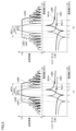
図5を用いて、隣接する弾性波共振子において共用反射器を用いる場合の反射特性について説明する。図5(a),(b)の各々においては、上段に反射器の反射係数の周波数特性が示され、下段に共振子のインピーダンスの周波数特性が示されている。図5において、実線LN50および実線LN60は直列腕共振子を示しており、破線LN51および破線LN61は並列腕共振子を示している。 Reflection characteristics when a common reflector is used in adjacent elastic wave resonators will be explained using FIG. 5. In each of FIGS. 5A and 5B, the frequency characteristics of the reflection coefficient of the reflector are shown in the upper row, and the frequency characteristics of the impedance of the resonator are shown in the lower row. In FIG. 5, a solid line LN50 and a solid line LN60 indicate a series arm resonator, and a broken line LN51 and a broken line LN61 indicate a parallel arm resonator.
図5を参照して、図1に示したようなラダー型フィルタにおいては、一般的に、直列腕共振子の共振周波数と並列腕共振子の反共振周波数とが略一致するように設計される。すなわち、直列腕共振子の反射器において反射係数が1に漸近する阻止域は、周波数f2~f4の間(図5(a)の領域AR10)となる。一方、並列腕共振子の反射器において反射係数が1に漸近する阻止域は、周波数f1~f3の間(図5(b)の領域AR11)となる。 Referring to FIG. 5, a ladder filter as shown in FIG. 1 is generally designed so that the resonant frequency of the series arm resonator and the anti-resonant frequency of the parallel arm resonator substantially match. . That is, the stopband where the reflection coefficient asymptotically approaches 1 in the reflector of the series arm resonator is between frequencies f2 and f4 (region AR10 in FIG. 5(a)). On the other hand, the stopband where the reflection coefficient asymptotically approaches 1 in the reflector of the parallel arm resonator is between frequencies f1 and f3 (area AR11 in FIG. 5(b)).
そのため、直列腕共振子と並列腕共振子の反射器を共用し、反射器の電極指のピッチを、どちらか一方の共振子のIDT電極の電極指ピッチに設定した場合には、周波数f2~f4の範囲(領域AR15)については反射率が確保できるものの、周波数f1~f2の範囲あるいは周波数f3~f4の範囲については反射率が大きく低下し得る。そうすると、この反射率が低下する領域において、一方の共振子からの弾性表面波が反射されずに他方の共振子に漏れ出してしまうため、フィルタ特性の劣化が生じ得る。 Therefore, if the series arm resonator and the parallel arm resonator share a reflector, and the pitch of the electrode fingers of the reflector is set to the pitch of the electrode fingers of the IDT electrode of either resonator, the frequency f2 ~ Although the reflectance can be ensured in the range of f4 (area AR15), the reflectance can be significantly reduced in the range of frequencies f1 to f2 or the range of frequencies f3 to f4. Then, in the region where the reflectance decreases, the surface acoustic wave from one resonator is not reflected and leaks to the other resonator, which may cause deterioration of filter characteristics.
一方で、本実施の形態1のように、共用反射器の電極指ピッチの少なくとも一部を2つの共振子の電極指ピッチの中間のピッチに設定した場合、共用反射器の反射係数は、たとえば図5における一点鎖線LN52のようになる。そうすると、図5(a)に示されるように、直列腕共振子についての阻止域は、周波数f2~f31の範囲(領域AR16)に拡大される。同様に、並列腕共振子についての阻止域は、図5(b)に示されるように、周波数f11~f3の範囲(領域AR17)に拡大される。すなわち、共用反射器の阻止域の下限周波数は、第1共振子の阻止域の下限周波数と第2共振子の阻止域の下限周波数との間になり、共用反射器の阻止域の上限周波数は、第1共振子の阻止域の上限周波数と第2共振子の阻止域の上限周波数との間になる。したがって、共用反射器の電極指ピッチをどちらか一方の共振子の電極指ピッチに統一した場合に比べて、フィルタ装置における阻止範囲を拡大することができ、結果としてフィルタ特性の劣化を抑制することができる。 On the other hand, when at least part of the electrode finger pitch of the shared reflector is set to an intermediate pitch between the electrode finger pitches of the two resonators as in the first embodiment, the reflection coefficient of the shared reflector is, for example, It becomes like the one-dot chain line LN52 in FIG. Then, as shown in FIG. 5(a), the stopband for the series arm resonator is expanded to the range of frequencies f2 to f31 (region AR16). Similarly, the stopband for the parallel arm resonator is expanded to the range of frequencies f11 to f3 (area AR17), as shown in FIG. 5(b). That is, the lower limit frequency of the stopband of the shared reflector is between the lower limit frequency of the stopband of the first resonator and the lower limit frequency of the stopband of the second resonator, and the upper limit frequency of the stopband of the shared reflector is , between the upper limit frequency of the stopband of the first resonator and the upper limit frequency of the stopband of the second resonator. Therefore, compared to the case where the electrode finger pitch of the shared reflector is unified to the electrode finger pitch of either resonator, the blocking range of the filter device can be expanded, and as a result, deterioration of filter characteristics can be suppressed. Can be done.
なお、実施の形態1において「阻止域」とは、反射係数のピーク値の70%の値よりも高い反射係数を有する周波数範囲を示す。実施の形態1において、阻止域の下限周波数は、各共振子の共振周波数に対応する。また、阻止域の上限周波数は、各共振子のインピーダンス特性において、ストップバンドリプル(図5における領域RG10,RG11)が出現し始める周波数に対応する。 Note that in the first embodiment, the "stopband" refers to a frequency range having a reflection coefficient higher than 70% of the peak value of the reflection coefficient. In the first embodiment, the lower limit frequency of the stopband corresponds to the resonant frequency of each resonator. Furthermore, the upper limit frequency of the stopband corresponds to the frequency at which stopband ripples (regions RG10 and RG11 in FIG. 5) begin to appear in the impedance characteristics of each resonator.
次に、図6~図9を用いて、高次モードのスプリアスの影響を低減するための構成についてより詳細に説明する。 Next, a configuration for reducing the influence of higher-order mode spurious will be described in more detail with reference to FIGS. 6 to 9.
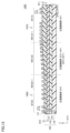
図6および図7は、実施の形態1に係る弾性波デバイスの上面図であり、図6は共用反射器の電極指の数が奇数の場合の弾性波デバイス100Aの上面図を示しており、図7は共用反射器の電極指の数が偶数の場合の弾性波デバイス100Bの上面図を示している。なお、図6および図7において、隣接する2つの弾性波共振子は、直列腕共振子同士でもよいし、並列腕共振子同士でもよい。あるいは、2つの弾性波共振子は、一方が直列腕共振子で他方が並列腕共振子であってもよい。
6 and 7 are top views of the acoustic wave device according to the first embodiment, and FIG. 6 is a top view of the
図6を参照して、弾性波デバイス100Aは、弾性波共振子101A,102Aと、弾性波共振子101A,102Aの間に配置された共用反射器REF12Aとを含む。弾性波デバイス100Aにおいては、弾性波共振子101AにおけるIDT電極IDT1Aのバスバー211と、弾性波共振子102AおけるIDT電極IDT2Aのバスバー221とが配線パターン200で接続されている。すなわち、バスバー211およびバスバー221は同電位である。
Referring to FIG. 6,
弾性波デバイス100Aにおいては、弾性波共振子101A,102Aおよび共用反射器REF12Aにおける電極指のピッチ、デューティおよび電極膜厚はいずれも同じとされている。したがって、弾性波共振子101Aおよび弾性波共振子102Aのメインモードおよび高次モードの信号の周波数帯域は一致している。
In the
共用反射器REF12Aは、弾性波共振子101Aの反射器REF1A-1と、弾性波共振子102Aの反射器REF2A-1との間に配置されている。反射器REF1A-1の電極指の数と共用反射器REF12Aの電極指の数の和は、反射器REF1A-2の電極指の数と同じである。また、反射器REF2A-1の電極指の数と共用反射器REF12Aの電極指の数の和は、反射器REF2A-2の電極指の数と同じである。上述のように、共用反射器REF12Aの有する電極指の数は奇数である。なお、弾性波共振子101Aの反射器REF1A-1の電極指の数と、弾性波共振子102Aの反射器REF2A-1ので電極指の数は同じに設定されている。
The shared reflector REF12A is arranged between the reflector REF1A-1 of the
弾性波共振子101AにおけるIDT電極IDT1Aにおいては、弾性波共振子102Aに最も近い電極指(領域RG1A内の電極指)、すなわち反射器REF1A-1に対向する電極指はバスバー210に接続されている。一方、弾性波共振子102AにおけるIDT電極IDT2Aにおいては、弾性波共振子101Aに最も近い電極指(領域RG2A内の電極指)、すなわち反射器REF2A-1に対向する電極指はバスバー221に接続されている。言い換えれば、共用反射器の有する電極指の数が奇数である場合には、IDT電極において相手側の弾性波共振子に最も近い電極指は、互いに逆の電位(逆極性)となるように配置される。
In the IDT electrode IDT1A in the
一方、図7の弾性波デバイス100Bにおいては、2つの弾性波共振子101B,102Bの間に配置される共用反射器REF12Bの電極指の数は偶数である。弾性波共振子101BにおけるIDT電極IDT1Bにおいては、弾性波共振子102Bに最も近い電極指(領域RG1B内の電極指)、すなわち反射器REF1B-1に対向する電極指はバスバー211に接続されている。そして、弾性波共振子102BにおけるIDT電極IDT2Bにおいては、弾性波共振子101Bに最も近い電極指(領域RG2B内の電極指)、すなわち反射器REF2B-1に対向する電極指はバスバー221に接続されている。言い換えれば、共用反射器の有する電極指の数が偶数である場合には、IDT電極において相手側の弾性波共振子に最も近い電極指は、同じ電位(同極性)となるように配置される。
On the other hand, in the
上記のようなIDT電極の電極指配置によって高次モードのスプリアスが低減される原理を、図8を用いて説明する。図8においては、共用反射器の電極指の数が奇数である弾性波デバイス100Bを例として説明する。なお、説明を容易にするために、反射器REF1A-1,2A-1については省略している。
The principle of reducing higher-order mode spurious by the electrode finger arrangement of the IDT electrode as described above will be explained using FIG. 8. In FIG. 8, an
図8を参照して、弾性波共振子101AのIDT電極IDT1Aにおいて、バスバー210に接続された電極指を電極指230とし、バスバー211に接続された電極指を電極指231とする。また、弾性波共振子102AのIDT電極IDT2Aにおいて、バスバー220に接続された電極指を電極指240とし、バスバー221に接続された電極指を電極指241とする。
Referring to FIG. 8, in IDT electrode IDT1A of
弾性波デバイス100Aにおいて、バスバー210,220の電位を高電位側のプラス電極とし、バスバー211,221の電位を低電位側のマイナス電極と仮定する。上述のように、バスバー211およびバスバー221は、配線パターン200で接続されているため同電位である。
In the
IDT電極においては、隣接する電極指のピッチは伝搬する弾性表面波の半波長(λ/2)となる。すなわち、各IDT電極を伝搬する弾性表面波は、プラス電極で高電位となり、マイナス電極で低電位となる。 In the IDT electrode, the pitch between adjacent electrode fingers is half the wavelength (λ/2) of the propagating surface acoustic wave. That is, the surface acoustic waves propagating through each IDT electrode have a high potential at the positive electrode and a low potential at the negative electrode.
メインモードの信号については、IDT電極IDT1Aからは、矢印AR1の方向に線LN1のような信号が伝搬する。また、IDT電極IDT2Aからは、矢印AR2の方向に線LN2のような信号が伝搬する。しかしながら、メインモードの信号は、2つのIDT電極間に配置された反射器によって反射されるため、相手側のIDT電極には到達しない。 Regarding the main mode signal, a signal like a line LN1 propagates from the IDT electrode IDT1A in the direction of the arrow AR1. Further, a signal as indicated by line LN2 is propagated from IDT electrode IDT2A in the direction of arrow AR2. However, the main mode signal does not reach the other IDT electrode because it is reflected by the reflector placed between the two IDT electrodes.
一方、高次モードの信号については、反射器では十分に反射されず、少なくとも一部が相手側のIDT電極へと通過する。図8においては、IDT電極IDT2Aからは、矢印AR3の方向に線LN3のような信号が伝搬する。共用反射器REF12Aの電極指の数が奇数(すなわち、共振子間の電極指の数が奇数)であるため、IDT電極IDT1Aにおいては、プラス電極(電極指230)においてIDT電極IDT2Aからの低電位の信号が受信され、マイナス電極(電極指231)においてIDT電極IDT2Aからの高電位の信号が受信される。逆に、IDT電極IDT1Aで発生して伝搬する高次モードの信号は、プラス電極(電極指230)において高電位となり、マイナス電極(電極指231)において低電位となる。すなわち、各電極指においては、一方の共振子からの高電位の信号と他方の共振子からの低電位の信号が受信されるため、各電極指において高次モードの信号が互いに打ち消し合うことになる。 On the other hand, high-order mode signals are not sufficiently reflected by the reflector, and at least a portion of them passes to the opposite IDT electrode. In FIG. 8, a signal as indicated by line LN3 propagates from IDT electrode IDT2A in the direction of arrow AR3. Since the number of electrode fingers of the shared reflector REF12A is an odd number (that is, the number of electrode fingers between resonators is an odd number), in the IDT electrode IDT1A, the low potential from the IDT electrode IDT2A is applied to the positive electrode (electrode finger 230). A signal of high potential from the IDT electrode IDT2A is received at the negative electrode (electrode finger 231). Conversely, a higher-order mode signal generated and propagated in the IDT electrode IDT1A has a high potential at the positive electrode (electrode finger 230) and a low potential at the negative electrode (electrode finger 231). In other words, each electrode finger receives a high-potential signal from one resonator and a low-potential signal from the other resonator, so the higher-order mode signals cancel each other out at each electrode finger. Become.
IDT電極間の反射器における電極指の数が奇数である場合、たとえばIDT電極IDT1Aで発生した高次モード信号は、反射器を通過した時点で位相が反転した状態となる。そのため、IDT電極IDT2Aにおいて反射器に対向する電極指については、IDT電極IDT1Aにおいて反射器に対向する電極指と逆の電位(逆極性)とすることによって、高次モード信号の影響を除去することができる。 If the number of electrode fingers in the reflector between the IDT electrodes is odd, the phase of the higher-order mode signal generated in the IDT electrode IDT1A, for example, will be inverted when it passes through the reflector. Therefore, the influence of higher-order mode signals can be removed by setting the electrode finger facing the reflector in the IDT electrode IDT2A to a potential (reverse polarity) opposite to that of the electrode finger facing the reflector in the IDT electrode IDT1A. Can be done.
なお、IDT電極間の反射器における電極指の数が偶数である場合には、反射器を通過した時点の高次モード信号の位相は、IDT電極から出力された信号と同位相となる。そのため、弾性波デバイス100Bにおいては、IDT電極IDT2Bにおいて反射器に対向する電極指を、IDT電極IDT1Bにおいて反射器に対向する電極指と同電位(同極性)とすることによって、高次モード信号の影響を除去することができる。
Note that when the number of electrode fingers in the reflector between the IDT electrodes is an even number, the phase of the higher-order mode signal at the time of passing through the reflector becomes the same phase as the signal output from the IDT electrode. Therefore, in the
本実施の形態1においては、上述のように、IDT電極と共用反射器との間に配置される反射器については、電極指が同じ数となるように設計されているため、IDT電極間の反射器における電極指の数が偶数であるか奇数であるかは、共用反射器の電極指によって定まる。 In the first embodiment, as described above, the reflectors arranged between the IDT electrode and the shared reflector are designed to have the same number of electrode fingers, so the number of electrode fingers between the IDT electrodes is Whether the number of electrode fingers in the reflector is even or odd is determined by the electrode fingers of the shared reflector.
なお、上述の例では、2つの弾性波共振子におけるメインモードの周波数が一致(すなわち、高次モードの周波数も一致)している場合を前提として説明したが、実際の設計においては、隣接する弾性波共振子の高次モードの周波数が完全に一致するとは限らない。以下に、高次モードのスプリアスの影響を除去可能な、弾性波共振子の周波数差について説明する。 In addition, in the above example, explanation was given on the assumption that the frequencies of the main modes in the two elastic wave resonators are the same (that is, the frequencies of the higher-order modes are also the same), but in actual design, The frequencies of higher-order modes of elastic wave resonators do not necessarily match completely. Below, a description will be given of the frequency difference of the elastic wave resonator that can eliminate the influence of spurious higher-order modes.
上述のように、高次モードの影響を除去するためには、一方の弾性波共振子から伝搬された高次モードの信号が、他方の弾性波共振子における高次モードの信号と逆位相となることが必要となる。音速v、周波数fおよび波長λの関係(v=fλ)から、音速が一定である場合には、周波数差は波長の差として表わすことができる。IDT電極を有するSAW共振子の場合、電極指のピッチは伝搬する弾性表面波の半波長(λ/2)に設定される。そのため、2つの弾性波共振子の電極指にピッチ差(すなわち、周波数差)があると、共用反射器における伝搬距離が長くなり、伝搬する電極指数が多くなるほど、相手方のIDT電極に到達したときの2つの信号の位相差が拡大する。この位相差がλ/4以下であれば、高次モードの影響を除去することが期待できる。 As mentioned above, in order to eliminate the influence of higher-order modes, the higher-order mode signal propagated from one elastic wave resonator must be in opposite phase to the higher-order mode signal in the other elastic wave resonator. It is necessary to become. From the relationship between sound speed v, frequency f, and wavelength λ (v=fλ), when the sound speed is constant, the frequency difference can be expressed as a wavelength difference. In the case of a SAW resonator having IDT electrodes, the pitch of the electrode fingers is set to a half wavelength (λ/2) of the propagating surface acoustic wave. Therefore, if there is a pitch difference (that is, a frequency difference) between the electrode fingers of two acoustic wave resonators, the propagation distance in the shared reflector becomes longer, and the more electrode fingers are propagated, the more when the electrode fingers of the other side are reached. The phase difference between the two signals increases. If this phase difference is λ/4 or less, it can be expected that the effects of higher-order modes can be eliminated.
図9は、信号の有効伝搬距離と2つの弾性波共振子の許容周波数差との関係を示した図である。ここで「有効伝搬距離」とは、2つの弾性波共振子を伝搬する信号の位相差をλ/4以下とすることができる限界の距離であり、波長(λ)であらわされている。図9の線LN10を参照すると、たとえば、有効伝搬距離が10λ(すなわち、共用反射器における電極指が20本)である場合には、2つの弾性波共振子の周波数差が2.5%以下であれば高次モードの影響を除去することが可能であることがわかる。上述のように、共用反射器における弾性表面波の伝搬距離が長くなるほど(すなわち、電極指数が多いほど)電極指のピッチ差が積算されるため、相手方のIDT電極に到達したときの2つの信号の位相差が拡大する。そのため、共用反射器による伝搬距離が長くなるほど許容周波数差は小さくなり、2つの弾性波共振子の周波数の一致度を高めることが必要となる。 FIG. 9 is a diagram showing the relationship between the effective propagation distance of a signal and the allowable frequency difference between two elastic wave resonators. Here, the "effective propagation distance" is the limit distance at which the phase difference between signals propagating through two elastic wave resonators can be λ/4 or less, and is expressed in wavelength (λ). Referring to line LN10 in FIG. 9, for example, when the effective propagation distance is 10λ (i.e., 20 electrode fingers in the shared reflector), the frequency difference between the two elastic wave resonators is 2.5% or less. It can be seen that it is possible to eliminate the influence of higher-order modes. As mentioned above, the longer the propagation distance of the surface acoustic wave in the shared reflector (that is, the larger the electrode index), the more the pitch difference between the electrode fingers is integrated, so the two signals when reaching the other IDT electrode The phase difference between increases. Therefore, the longer the propagation distance by the shared reflector, the smaller the allowable frequency difference becomes, and it becomes necessary to increase the degree of coincidence between the frequencies of the two elastic wave resonators.
波長を単位とした長さを「波長換算長さ(N)」とした場合、許容周波数差は以下の式(1)のように表すことができ、これが図9の線LN10に対応する。 When the length in units of wavelength is defined as "wavelength conversion length (N)," the allowable frequency difference can be expressed as in the following equation (1), which corresponds to line LN10 in FIG. 9.
許容周波数差[%]=25/N …(1)
ここで、共用反射器の電極指の数をnとすると、波長換算長さNと電極指数nとの関係はn=2Nとなるので、当該関係と式(1)とから式(2)が得られる。Allowable frequency difference [%] = 25/N…(1)
Here, if the number of electrode fingers of the shared reflector is n, the relationship between the wavelength conversion length N and the electrode index n is n = 2N, so from this relationship and equation (1), equation (2) can be obtained. can get.
許容周波数差[%]=50/n …(2)
本開示において「高次モード周波数が一致する」とは、許容周波数差が0%から(50/n)%の範囲内であることを意味する。Allowable frequency difference [%] = 50/n...(2)
In the present disclosure, "higher mode frequencies match" means that the allowable frequency difference is within the range of 0% to (50/n)%.
小型化の観点からは、共用する電極指の数を多くすることが好ましいが、共用する電極指の数が多くなると、共振子間の周波数の一致度を高くすることが必要となる。したがって、共用反射器のサイズについては、2つの共振子の周波数差および弾性波デバイス全体のサイズに応じて適宜選択される。 From the viewpoint of miniaturization, it is preferable to increase the number of shared electrode fingers, but as the number of shared electrode fingers increases, it is necessary to increase the frequency matching between resonators. Therefore, the size of the shared reflector is appropriately selected depending on the frequency difference between the two resonators and the overall size of the acoustic wave device.
(変形例)
実施の形態1の弾性波デバイスにおいては、IDT電極および反射器における電極指が、電極指に接続されたバスバーに対して直交する方向に延在する構成について説明した。変形例の弾性波デバイスにおいては、IDT電極および反射器の電極指が、バスバーに対して傾斜配置された構成について説明する。(Modified example)
In the acoustic wave device of
図10は、変形例に係る弾性波デバイス100Cの上面図である。弾性波デバイス100Cにおいては、弾性波共振子101C,102Cと、弾性波共振子101C,102Cの間に配置された共用反射器REF12Cとを含む。
FIG. 10 is a top view of an
弾性波共振子101Cは、IDT電極IDT1Cと、IDT電極IDT1Cの両側に配置された反射器REF1C-1,REF1C-2とを含む。弾性波共振子102Cは、IDT電極IDT2Cと、IDT電極IDT2Cの両側に配置された反射器REF2C-1,REF2C-2とを含む。
The
共用反射器REF12Cは、反射器REF1C-1と反射器REF2C-1との間に配置されている。反射器REF1C-1の電極指の数と共用反射器REF12Cの電極指の数の和は、反射器REF1C-2の電極指の数と同じである。また、反射器REF2C-1の電極指の数と共用反射器REF12Cの電極指の数の和は、反射器REF2C-2の電極指の数と同じである。弾性波デバイス100Cにおいて、弾性波共振子101C,102Cおよび共用反射器REF12Cの電極指は、バスバーに対して斜めに接続されている。電極指とバスバーとのなす角は、0°より大きく90°より小さい。
The shared reflector REF12C is arranged between the reflector REF1C-1 and the reflector REF2C-1. The sum of the number of electrode fingers of the reflector REF1C-1 and the number of electrode fingers of the shared reflector REF12C is the same as the number of electrode fingers of the reflector REF1C-2. Further, the sum of the number of electrode fingers of the reflector REF2C-1 and the number of electrode fingers of the shared reflector REF12C is the same as the number of electrode fingers of the reflector REF2C-2. In the
弾性波共振子においては、電極指に直交する方向に弾性表面波が伝搬する。たとえば、弾性波デバイス100Cにおいては、弾性波共振子101Cからの信号は図10の矢印AR11の方向に伝搬し、弾性波共振子102Cからの信号は図10の矢印AR12の方向に伝搬する。変形例の弾性波デバイス100Cのように、隣接する弾性波共振子についてバスバーに対して電極指を傾斜配置することによって、一方の弾性波共振子における弾性表面波の伝搬方向を、他方の弾性波共振子のIDT電極における電極指の交叉幅領域外とすることができる。したがって、共用反射器から弾性表面波がリークした場合における他方の弾性波共振子への影響をさらに低減することができる。
In an elastic wave resonator, surface acoustic waves propagate in a direction perpendicular to the electrode fingers. For example, in the
なお、図10の弾性波デバイス100Cは、共用反射器の電極指数が奇数である図6の弾性波デバイス100Aの電極指を傾斜配置させた構成に対応しているが、共用反射器の電極指数が偶数である図7の弾性波デバイス100Bについても、電極指を傾斜配置させてもよい。
Note that the
[実施の形態2]
実施の形態1においては、隣接する2つの弾性波共振子におけるメインモードの周波数が一致している場合について説明した。しかしながら、実際の設計においては、隣接する弾性波共振子のメインモードの周波数が異なる場合がある。そうすると、共用反射器を用いる場合に、共用反射器における電極指の数に応じてIDT電極の電極指の極性を調整するだけでは、高次モードのスプリアスを除去できない場合が生じ得る。[Embodiment 2]
In the first embodiment, a case has been described in which the main mode frequencies of two adjacent elastic wave resonators are the same. However, in actual design, the frequencies of the main modes of adjacent elastic wave resonators may differ. In this case, when a shared reflector is used, it may not be possible to remove higher-order mode spurious noise simply by adjusting the polarity of the electrode fingers of the IDT electrode according to the number of electrode fingers in the shared reflector.
実施の形態2においては、隣接する弾性波共振子のメインモードの周波数が異なる場合において、メインモードの周波数を維持しつつ、高次モードのスプリアスの周波数を調整することによって、当該スプリアスの影響を低減する構成について説明する。 In the second embodiment, when the frequencies of the main modes of adjacent elastic wave resonators are different, the influence of the spurious is reduced by adjusting the frequency of the spurious of the higher-order mode while maintaining the frequency of the main mode. A configuration for reducing this will be explained.
一般的に、共振子において、波長、圧電層膜厚、電極膜厚、あるいはデューティのような共振子の構造パラメータに対する周波数依存性は、メインモードと高次モードとで異なる。そのため、このような特性を利用することよって、メインモードの周波数を維持しながら、高次モードの周波数をシフトさせる。 Generally, in a resonator, the frequency dependence on structural parameters of the resonator, such as wavelength, piezoelectric layer thickness, electrode thickness, or duty, differs between the main mode and the higher-order modes. Therefore, by utilizing such characteristics, the frequency of the higher-order mode is shifted while maintaining the frequency of the main mode.
図11は、共振子の各構造パラメータ(波長,圧電層膜厚,電極膜厚、デューティ)に対する高次モードの周波数感度比を示す図である。周波数感度比とは、メインモードの共振周波数の変化率を1.00としたときの、高次モードの周波数の変化率を示したものである。周波数感度比の符号は、共振子の各構造パラメータの増加に対して、メインモードの共振周波数および/または高次モードの周波数が増加する場合は正、メインモードの共振周波数および/または高次モードの周波数が減少する場合は負、として表わされる。周波数感度比の絶対値が1.00より大きい場合、当該構造パラメータを変化させた場合の高次モードの周波数の変化率が、メインモードの周波数の変化率よりも大きいことを示す。 FIG. 11 is a diagram showing the frequency sensitivity ratio of higher-order modes with respect to each structural parameter (wavelength, piezoelectric layer thickness, electrode thickness, duty) of the resonator. The frequency sensitivity ratio indicates the rate of change in the frequency of higher-order modes when the rate of change in the resonance frequency of the main mode is 1.00. The sign of the frequency sensitivity ratio is positive if the resonant frequency of the main mode and/or the frequency of higher-order modes increases with respect to the increase in each structural parameter of the resonator; It is expressed as negative if the frequency of decreases. If the absolute value of the frequency sensitivity ratio is greater than 1.00, it indicates that the rate of change in the frequency of the higher-order mode is greater than the rate of change in the frequency of the main mode when the structural parameter is changed.
なお、圧電層の膜厚においては、圧電層の材料および厚さにより、メインモード共振周波数と高次モード周波数について、共振子の各構造パラメータに対する依存傾向が変化する。圧電層がLTもしくはLNであり、その厚みが電極指ピッチで定まる波長λに対して2λ以下である場合は、周波数感度比は次のようになる。すなわち、メインモードがたとえばA0モード(0次反対称モード)あるいはSH0モード(0次剪断水平モード)である場合には、周波数感度比の符号は正となる。一方、メインモードがたとえばS0モード(対称モード)、SH1モード(1次剪断水平モードで)、A1モード(1次反対称モード)、およびこれ以上の高次の振動モードである場合には、周波数感度比の符号は負となる。また、高次モードがたとえばA0モードあるいはSH0モードである場合には周波数感度比の符号は正となり、高次モードがたとえばS0モード、SH1モード、A1モード、およびこれ以上の高次の振動モードである場合には周波数感度比の符号は負となる。高次モードにおいては、振動モードによって周波数感度比の絶対値も変化する。一方、圧電層の厚みが2λ~5λの範囲の場合、上記のような依存傾向は無くなる。 Note that the dependence of the main mode resonance frequency and higher-order mode frequency on each structural parameter of the resonator changes depending on the material and thickness of the piezoelectric layer. When the piezoelectric layer is LT or LN and its thickness is 2λ or less with respect to the wavelength λ determined by the electrode finger pitch, the frequency sensitivity ratio is as follows. That is, when the main mode is, for example, A0 mode (zero-order antisymmetric mode) or SH0 mode (zero-order shear horizontal mode), the sign of the frequency sensitivity ratio is positive. On the other hand, if the main modes are, for example, S0 mode (symmetric mode), SH1 mode (first-order shear horizontal mode), A1 mode (first-order antisymmetric mode), and higher-order vibration modes, the frequency The sign of the sensitivity ratio is negative. Furthermore, when the higher-order mode is, for example, A0 mode or SH0 mode, the sign of the frequency sensitivity ratio is positive, and when the higher-order mode is, for example, S0 mode, SH1 mode, A1 mode, and higher-order vibration modes, the sign of the frequency sensitivity ratio is positive. In some cases, the sign of the frequency sensitivity ratio is negative. In higher-order modes, the absolute value of the frequency sensitivity ratio also changes depending on the vibration mode. On the other hand, when the thickness of the piezoelectric layer is in the range of 2λ to 5λ, the above dependency tendency disappears.
図11は、メインモードにSH0モード、高次モードにS0モードを用いた場合の周波数感度比を示す。なお、後述する第1例~第4例においても、これらのモードを用いた場合について示している。 FIG. 11 shows the frequency sensitivity ratio when the S0 mode is used as the main mode and the S0 mode is used as the higher-order mode. Note that the first to fourth examples described later also show cases in which these modes are used.
図11を参照して、たとえば波長(すなわち、電極指ピッチ)を変化させた場合には、メインモードの共振周波数の変化率-1.00に対して、高次モードの周波数の変化率は-0.67となる。すなわち、波長を変化させた場合、メインモードよりも高次モードの方が周波数変化が小さくなる。 Referring to FIG. 11, for example, when the wavelength (i.e., electrode finger pitch) is changed, the rate of change in the frequency of the higher-order mode is -1.00 for the rate of change in the resonance frequency of the main mode. It becomes 0.67. That is, when changing the wavelength, the frequency change is smaller in the higher-order mode than in the main mode.
圧電層膜厚を変化させた場合の高次モードの周波数感度比は-2.40である。この場合、メインモードの共振周波数が高くなると、高次モードの周波数は、メインモードよりも大きな度合いで低くなる。同様に、電極指のデューティを変化させた場合の高次モードの周波数感度比は0.55であり、電極指の膜厚を変化させた場合の高次モードの周波数感度比は0.70である。すなわち、電極指のデューティおよび膜厚を変化させた場合、メインモードよりも高次モードの方が周波数変化率が小さくなる。 The frequency sensitivity ratio of higher-order modes when the piezoelectric layer thickness is changed is -2.40. In this case, as the resonant frequency of the main mode increases, the frequency of the higher-order modes decreases to a greater extent than the main mode. Similarly, the frequency sensitivity ratio of higher-order modes when changing the duty of the electrode fingers is 0.55, and the frequency sensitivity ratio of higher-order modes when changing the film thickness of the electrode fingers is 0.70. be. That is, when the duty and film thickness of the electrode fingers are changed, the frequency change rate is smaller in the higher-order mode than in the main mode.
図11に示されるように、高次モードの周波数感度比は、構造パラメータによって特性が異なっている。そのため、メインモードの共振周波数を波長(電極指ピッチ)以外の構造パラメータで変化させ、その後、波長を調整してメインモードの共振周波数を元に戻すと、メインモードの共振周波数を同じ状態としたままで、高次モードの周波数を異なる周波数にすることができる。 As shown in FIG. 11, the frequency sensitivity ratio of the higher-order mode has different characteristics depending on the structural parameters. Therefore, if the main mode resonance frequency is changed by a structural parameter other than the wavelength (electrode finger pitch) and then the wavelength is adjusted to return the main mode resonance frequency to its original state, the main mode resonance frequency remains the same. The frequency of the higher-order mode can be set to a different frequency.
以下、圧電層膜厚を変化させた例を第1例に示し、電極指のデューティを変化させた例を第2例に示し、電極指の膜厚を変化させた例を第3例に示す。 Below, the first example shows an example in which the piezoelectric layer thickness is changed, the second example shows an example in which the duty of the electrode fingers is changed, and the third example shows an example in which the electrode finger thickness is changed. .
(第1例)
第1例においては、隣接する2つの弾性波共振子における圧電層の膜厚を変更することによって、高次モードのスプリアスの周波数を調整する場合について説明する。(1st example)
In the first example, a case will be described in which the frequency of spurious in a higher order mode is adjusted by changing the thickness of the piezoelectric layer in two adjacent acoustic wave resonators.
図12は、実施の形態2の第1例に係る弾性波デバイス100Dの断面図である。図12を参照して、弾性波デバイス100Dは、弾性波共振子101D,102Dと、弾性波共振子101D,102Dの間に配置された共用反射器REF12Dとを含む。
FIG. 12 is a cross-sectional view of an
第1例においては、弾性波共振子101Dのメインモードの周波数は、弾性波共振子102Dのメインモードの周波数よりも高く設定されている。すなわち、弾性波共振子101DにおけるIDT電極IDT1Dおよび反射器REF1Dの電極指ピッチ(PT1)は、弾性波共振子102DにおけるIDT電極IDT2Dおよび反射器REF2Dの電極指ピッチ(PT2)よりも狭い。そして、共用反射器REF12Dの電極指の少なくとも一部は、電極指ピッチPT1と電極指ピッチPT2の間のピッチで形成されている。
In the first example, the main mode frequency of the
基板105において、弾性波共振子101Dが配置された領域の圧電層110の膜厚はBT1に設定されており、弾性波共振子102Dが配置された領域の圧電層110の膜厚はBT2(BT1>BT2)に設定されている。そして、共用反射器REF12Dが配置された領域の少なくとも一部の圧電層110は、弾性波共振子101Dが配置された領域の圧電層110の膜厚BT1よりも薄く、かつ、弾性波共振子102Dが配置された領域の圧電層110の膜厚BT2よりも厚く設定されている。図12においては、共用反射器REF12Dにおける電極指の膜厚は、弾性波共振子101Dから弾性波共振子102Dに向かって徐々に薄くなっている。
In the
図13は、メインモードおよび高次モードにおける、圧電層膜厚と板波音速との関係を示す図である。図13においては、横軸には波長によって規格化された圧電層110の膜厚(h/λ)が示されており、縦軸には板波音速が示されている。図13において、実線LN20はメインモードの場合を示しており、破線LN21は高次モードの一例の場合を示している。
FIG. 13 is a diagram showing the relationship between the piezoelectric layer thickness and the plate wave sound velocity in the main mode and higher-order mode. In FIG. 13, the horizontal axis shows the film thickness (h/λ) of the
図13を参照して、メインモードについては、圧電層の膜厚が薄くなると板波音速が低くなり、圧電層の膜厚が所定よりも厚くなると音速はほぼ一定となる傾向を有している。v=fλの関係から、波長λ(すなわち電極指ピッチ)が一定の場合でも、音速vが変化すると周波数fが変化する。すなわち、圧電層膜厚が厚くなると周波数が高くなり、圧電層膜厚が薄くなると周波数が低くなる。一方で、高次モードについては、メインモードとは異なり、圧電層の膜厚が薄くなるほど音速(周波数)が高くなり、圧電層の膜厚が厚くなるほど音速(周波数)が低下する傾向を有している。 Referring to FIG. 13, regarding the main mode, as the film thickness of the piezoelectric layer becomes thinner, the plate wave sound speed decreases, and when the film thickness of the piezoelectric layer becomes thicker than a predetermined value, the sound speed tends to be almost constant. . From the relationship v=fλ, even if the wavelength λ (that is, the electrode finger pitch) is constant, the frequency f changes when the sound speed v changes. That is, as the thickness of the piezoelectric layer increases, the frequency increases, and as the thickness of the piezoelectric layer decreases, the frequency decreases. On the other hand, for higher-order modes, unlike the main mode, the thinner the piezoelectric layer is, the higher the sound speed (frequency) is, and the thicker the piezoelectric layer is, the faster the sound speed (frequency) is. ing.
図11および図13に示されるように、圧電層の膜厚に対する周波数の変化度合い(周波数感度比の絶対値)は、メインモードよりも高次モードの方が大きく、変化方向(周波数感度比の符号)が逆になる。そのため、圧電層の膜厚を薄くしてメインモードの共振周波数を低くし、その後、電極指ピッチを調整してメインモードの共振周波数を元に戻した場合、メインモードの周波数を維持した状態で、高次モードの周波数を高くすることができる。 As shown in FIGS. 11 and 13, the degree of change in frequency (absolute value of frequency sensitivity ratio) with respect to the film thickness of the piezoelectric layer is larger in higher-order modes than in the main mode, and the direction of change (absolute value of frequency sensitivity ratio) is larger in higher-order modes than in the main mode. sign) is reversed. Therefore, if the thickness of the piezoelectric layer is made thinner to lower the main mode resonance frequency, and then the electrode finger pitch is adjusted to return the main mode resonance frequency to its original value, the main mode frequency remains the same. , the frequency of higher-order modes can be increased.
図12の弾性波デバイス100Dの場合には、弾性波共振子101Dが配置される圧電層110の膜厚を弾性波共振子102Dが配置される圧電層110の膜厚に比べて厚くすることによって、弾性波共振子101Dにおける高次モードの周波数を低下させ、弾性波共振子102Dの高次モードの周波数に近づけている。あるいは、逆に、弾性波共振子102Dが配置される圧電層110の膜厚を弾性波共振子101Dが配置される圧電層110の膜厚に比べて薄くすることによって、弾性波共振子102Dにおける高次モードの周波数を高くして、弾性波共振子101Dの高次モードの周波数に近づけている。なお、圧電層110の膜厚を変更することによって、メインモードの周波数が多少変化する場合があるが、そのような場合には、対象となる弾性波共振子のピッチを修正することにより所望の周波数に調整することができる。
In the case of the
このように、弾性波デバイスにおいて、共用反射器を介して隣接配置された2つの弾性波共振子のメインモードの周波数が異なる場合に、各弾性波共振子が配置される圧電層の膜厚と電極指ピッチを調整することによって、高次モードの信号の周波数を一致させることができる。そして、共用反射器の電極指の数が奇数であるか偶数であるかに応じて、IDT電極において最も共用反射器側に配置された電極指の極性を変更することによって、メインモードの周波数が異なる場合であっても高次モードのスプリアスの影響を低減することができる。 In this way, in an acoustic wave device, when the main mode frequencies of two acoustic wave resonators placed adjacent to each other via a shared reflector are different, the film thickness of the piezoelectric layer on which each elastic wave resonator is placed is By adjusting the electrode finger pitch, the frequencies of higher-order mode signals can be matched. Then, depending on whether the number of electrode fingers of the shared reflector is odd or even, the frequency of the main mode can be adjusted by changing the polarity of the electrode finger located closest to the shared reflector in the IDT electrode. Even in different cases, the influence of higher-order mode spurious can be reduced.
なお、共用反射器REF12Dにおいては、電極指の全体が中間的なピッチで形成されていてもよいし、弾性波共振子101Dから弾性波共振子102Dに向かって徐々にピッチが変更される構成であってもよい。また、弾性波共振子101Dから弾性波共振子102Dに向かって段階的にピッチが変更される構成であってもよい。
In the shared reflector REF12D, the entire electrode fingers may be formed with an intermediate pitch, or the pitch may be gradually changed from the
また、共用反射器REF12Dが配置された領域の圧電層110の膜厚は、全体が中間的な膜厚であってもよいし、図12のように弾性波共振子101Dから弾性波共振子102Dに向かって徐々に圧電層110の膜厚が変更される構成であってもよい。また、弾性波共振子101Dから弾性波共振子102Dに向かって段階的に圧電層110の膜厚が変更される構成であってもよい。ただし、電極指のピッチと圧電層110の膜厚については、図13で説明したように、波長により規格化した圧電層膜厚(h/λ)が略一定となるように設定することが好ましい。
Further, the thickness of the
図14は、第1例についての実施例とその比較例の具体的な仕様を示した図である。図14の上段(図14(a))には比較例が示されており、下段(図14(b))に実施例が示されている。なお、図14の例においては、比較例および実施例のいずれにおいても電極指のデューティは0.5である。 FIG. 14 is a diagram showing specific specifications of an example of the first example and a comparative example thereof. A comparative example is shown in the upper part of FIG. 14 (FIG. 14(a)), and an example is shown in the lower part (FIG. 14(b)). In the example of FIG. 14, the duty of the electrode finger is 0.5 in both the comparative example and the example.
比較例においては、共振子1および共振子2の圧電層膜厚は、いずれも600nmに設定されている。比較例では、共振子1のメインモードの周波数は2464.282MHzであり、高次モードの周波数は3106.941MHzである。また、共振子2のメインモードの周波数は2361.513MHzであり、高次モードの周波数は3019.257MHzである。
In the comparative example, the thicknesses of the piezoelectric layers of
一方、実施例においては、共振子2の圧電層膜厚が500nmに変更され、さらに波長が1.607μmに調整されている。すなわち、共振子2の圧電層膜厚を薄くしてメインモードの共振周波数を低くし、波長を短く調整することでメインモードの共振周波数を元に戻している。これによって、当該実施例においては、共振子2のメインモードの周波数が2361.312MHzとなり、共振子2の高次モードの周波数が3017.580MHzと高くなっている。したがって、共振子2については、メインモードの周波数を維持しながら、高次モードの周波数を共振子1の場合に一致させることができている。このように、メインモードの周波数が異なる場合でも、圧電層膜厚を調整することによって、高次モードのスプリアスによる影響を除去することが可能となる。
On the other hand, in the example, the thickness of the piezoelectric layer of the
(第2例)
第2例においては、隣接する2つの弾性波共振子における電極指のデューティを変更することによって、高次モードのスプリアスの周波数を調整する場合について説明する。(2nd example)
In a second example, a case will be described in which the frequency of spurious higher-order modes is adjusted by changing the duty of electrode fingers in two adjacent acoustic wave resonators.
図15は、実施の形態2の第2例に係る弾性波デバイス100Eの断面図である。図15を参照して、弾性波デバイス100Eは、弾性波共振子101E,102Eと、弾性波共振子101E,102Eの間に配置された共用反射器REF12Eとを含む。
FIG. 15 is a cross-sectional view of an
第2例においては、弾性波共振子101Eのメインモードの周波数は、弾性波共振子102Eのメインモードの周波数よりも低く設定されている。すなわち、弾性波共振子101EにおけるIDT電極IDT1Eおよび反射器REF1Eの電極指ピッチ(PT1)は、弾性波共振子102EにおけるIDT電極IDT2Eおよび反射器REF2Eの電極指ピッチ(PT2)よりも広い。そして、共用反射器REF12Eの電極指の少なくとも一部は、電極指ピッチPT1と電極指ピッチPT2の間のピッチで形成されている。
In the second example, the main mode frequency of the
なお、共用反射器REF12Eにおいては、電極指の全体が中間的なピッチで形成されていてもよいし、弾性波共振子101Eから弾性波共振子102Eに向かって徐々にピッチが変更される構成であってもよい。また、弾性波共振子101Eから弾性波共振子102Eに向かって段階的にピッチが変更される構成であってもよい。
In the shared reflector REF12E, the entire electrode fingers may be formed with an intermediate pitch, or the pitch may be gradually changed from the
弾性波デバイス100Eにおいては、弾性波共振子101Eにおける電極指のデューティ(第1デューティ)はDT1に設定されており、弾性波共振子102Eにおける電極指のデューティ(第2デューティ)はDT2(DT1>DT2)に設定されている。そして、共用反射器REF12Eにおける電極指の少なくとも一部は、上記の第1デューティDT1および第2デューティDT2の間の中間的なデューティで形成されている。言い換えれば、共用反射器REF12Eにおける電極指の少なくとも一部は、第1デューティDT1よりも小さく、かつ、第2デューティDT2よりも大きく形成されている。たとえば、好ましくは、共用反射器REF12Eの電極指のデューティは、弾性波共振子101Eから弾性波共振子102Eに向かって徐々に、あるいは段階的に小さくなるように設定される。
In the
図16は、高次モード周波数とIDT電極のデューティとの関係を説明するための図である。図16においては、横軸にはメインモードの波長が示されており、縦軸に高次モード周波数が示されている。図16において、線LN30はIDT電極のデューティが0.4の場合を示しており、線LN31はIDT電極のデューティが0.5の場合を示しており、線LN32はIDT電極のデューティが0.6の場合を示している。これらより、メインモードの周波数が同じ場合であっても、デューティが大きくなるほど高次モードの周波数は低下する傾向にあることがわかる。 FIG. 16 is a diagram for explaining the relationship between the higher-order mode frequency and the duty of the IDT electrode. In FIG. 16, the horizontal axis shows the wavelength of the main mode, and the vertical axis shows the higher-order mode frequency. In FIG. 16, line LN30 shows the case where the duty of the IDT electrode is 0.4, line LN31 shows the case where the duty of the IDT electrode is 0.5, and line LN32 shows the case where the duty of the IDT electrode is 0.4. 6 is shown. From these results, it can be seen that even when the main mode frequency is the same, the higher the duty becomes, the higher-order mode frequency tends to decrease.
メインモードの共振周波数は、基本的には電極指のピッチにより定まる。しかしながら、電極指ピッチが同じであっても、電極指の質量が増減すると、質量付加効果によってメインモードの共振周波数が変化し得る。具体的には、電極指の質量が増加すると共振周波数は低くなり、電極指の質量が減少すると共振周波数は高くなる。そのため、デューティを変化させると電極指の電極幅が変化して質量が増減し、メインモードの共振周波数が変化する。そして、図11に示したように、デューティに対する周波数感度は、メインモードよりも高次モードの方が小さい。したがって、電極指のデューティを小さくしてメインモードの共振周波数を高くし、その後、電極指ピッチを調整してメインモードの共振周波数を元に戻した場合、メインモードの周波数を維持した状態で、高次モードの周波数を低くすることができる。 The resonance frequency of the main mode is basically determined by the pitch of the electrode fingers. However, even if the electrode finger pitch is the same, if the mass of the electrode fingers increases or decreases, the resonance frequency of the main mode may change due to the mass addition effect. Specifically, as the mass of the electrode finger increases, the resonant frequency decreases, and as the mass of the electrode finger decreases, the resonant frequency increases. Therefore, when the duty is changed, the electrode width of the electrode finger changes, the mass increases or decreases, and the resonance frequency of the main mode changes. As shown in FIG. 11, the frequency sensitivity to duty is smaller in the higher-order mode than in the main mode. Therefore, if you increase the main mode resonance frequency by decreasing the duty of the electrode fingers and then return the main mode resonance frequency to its original value by adjusting the electrode finger pitch, while maintaining the main mode frequency, The frequency of higher-order modes can be lowered.
このように、隣接する弾性波共振子において、デューティと電極指ピッチを調整することによって、メインモードの周波数を変化させることなく、高次モードの周波数を調整して一致させることができる。したがって、弾性波共振子のメインモードの周波数が異なる場合であっても、高次モードのスプリアスを除去することが可能となる。 In this manner, by adjusting the duty and the electrode finger pitch in adjacent elastic wave resonators, it is possible to adjust and match the frequencies of higher-order modes without changing the frequency of the main mode. Therefore, even if the frequencies of the main modes of the elastic wave resonators are different, it is possible to remove spurious signals in higher-order modes.
図17は、第2例についての実施例とその比較例の具体的な仕様を示した図である。図17の上段(図17(a))には比較例が示されており、下段(図17(b))に実施例が示されている。 FIG. 17 is a diagram showing specific specifications of an example of the second example and a comparative example thereof. A comparative example is shown in the upper part of FIG. 17 (FIG. 17(a)), and an example is shown in the lower part (FIG. 17(b)).
比較例においては、共振子1および共振子2のデューティは、いずれも0.5に設定されている。比較例では、共振子1のメインモードの周波数は2464.282MHzであり、高次モードの周波数は3106.941MHzである。また、共振子2のメインモードの周波数は2469.837MHzであり、高次モードの周波数は3111.626MHzである。
In the comparative example, the duties of
一方、実施例においては、共振子2のデューティが0.4に設定され、さらに波長が1.559226μmに設定されている。共用反射器においては、共振子1から共振子2に向かって、電極指のデューティが0.5から0.4に徐々に変化している。すなわち、共振子2のデューティを小さくしてメインモードの共振周波数を高くし、波長を長く調整することでメインモードの共振周波数を元に戻している。これによって、当該実施例においては、共振子2のメインモードの周波数が2469.837MHzとなり、共振子2の高次モードの周波数が3106.941MHzと低くなっている。したがって、共振子2については、メインモードの周波数を維持しながら、高次モードの周波数を共振子1の場合に一致させることができている。このように、メインモードの周波数が異なる場合でも、弾性波共振子の電極指のデューティを調整することによって、高次モードのスプリアスによる影響を除去することが可能となる。
On the other hand, in the example, the duty of the
(第3例)
第3例においては、隣接する2つの弾性波共振子における電極指の膜厚を変更することによって、高次モードのスプリアスの周波数を調整する場合について説明する。(3rd example)
In a third example, a case will be described in which the frequency of spurious signals in higher-order modes is adjusted by changing the film thickness of electrode fingers in two adjacent acoustic wave resonators.
図18は、実施の形態2の第3例に係る弾性波デバイス100Fの断面図である。図18を参照して、弾性波デバイス100Fは、弾性波共振子101F,102Fと、弾性波共振子101F,102Fの間に配置された共用反射器REF12Fとを含む。
FIG. 18 is a cross-sectional view of an
第3例においては、弾性波共振子101Fのメインモードの周波数は、弾性波共振子102Fのメインモードの周波数よりも低く設定されている。すなわち、弾性波共振子101FにおけるIDT電極IDT1Fおよび反射器REF1Fの電極指ピッチ(PT1)は、弾性波共振子102FにおけるIDT電極IDT2Fおよび反射器REF2Fの電極指ピッチ(PT2)よりも広い。そして、共用反射器REF12Fの電極指の少なくとも一部は、電極指ピッチPT1と電極指ピッチPT2の間のピッチで形成されている。
In the third example, the main mode frequency of the
なお、共用反射器REF12Fにおいては、電極指の全体が中間的なピッチで形成されていてもよいし、弾性波共振子101Fから弾性波共振子102Fに向かって徐々にピッチが変更される構成であってもよい。また、弾性波共振子101Fから弾性波共振子102Fに向かって段階的にピッチが変更される構成であってもよい。
In the shared reflector REF12F, the entire electrode fingers may be formed with an intermediate pitch, or the pitch may be gradually changed from the
弾性波デバイス100Fにおいては、弾性波共振子101Fにおける電極指の膜厚はET1に設定されており、弾性波共振子102Fにおける電極指の膜厚はET2(ET1<ET2)に設定されている。そして、共用反射器REF12Fにおける電極指の少なくとも一部は、上記の膜厚ET1および膜厚ET2の間の中間的な膜厚で形成されている。言い換えれば、共用反射器REF12Fにおける電極指の少なくとも一部は、弾性波共振子101Fにおける電極指の膜厚ET1よりも厚く、かつ、弾性波共振子102Fにおける電極指の膜厚ET2よりも薄い。好ましくは、共用反射器REF12Fの電極指の膜厚は、弾性波共振子101Fから弾性波共振子102Fに向かって徐々に、あるいは段階的に厚くなるように設定される。
In the
図19は、高次モード周波数とIDT電極の膜厚との関係を説明するための図である。図19においては、横軸にはメインモードの波長が示されており、縦軸に高次モード周波数が示されている。図19において、線LN40はIDT電極の膜厚が111nmの場合を示しており、線LN41はIDT電極の膜厚が121nmの場合を示しており、線LN42はIDT電極の膜厚が131nmの場合を示している。これらより、メインモードの周波数が同じ場合であっても、IDT電極の膜厚が厚くなるほど高次モードの周波数は低下する傾向にあることがわかる。 FIG. 19 is a diagram for explaining the relationship between the higher-order mode frequency and the film thickness of the IDT electrode. In FIG. 19, the horizontal axis shows the wavelength of the main mode, and the vertical axis shows the higher-order mode frequency. In FIG. 19, line LN40 shows the case where the film thickness of the IDT electrode is 111 nm, line LN41 shows the case where the film thickness of the IDT electrode is 121 nm, and line LN42 shows the case where the film thickness of the IDT electrode is 131 nm. It shows. From these results, it can be seen that even when the frequency of the main mode is the same, the frequency of the higher-order mode tends to decrease as the film thickness of the IDT electrode becomes thicker.
第2例のデューティを変化させた場合と同様に、IDT電極の膜厚を厚くすると電極の質量が増えるため、質量付加効果によってメインモードの共振周波数が低下する。そして、図11に示したように、IDT電極の膜厚に対する周波数感度は、メインモードよりも高次モードの方が小さい。したがって、IDT電極の膜厚を厚くしてメインモードの共振周波数を低くし、その後、電極指ピッチを調整してメインモードの共振周波数を元に戻した場合、メインモードの周波数を維持した状態で、高次モードの周波数を低くすることができる。 As in the case of changing the duty in the second example, increasing the film thickness of the IDT electrode increases the mass of the electrode, so the resonance frequency of the main mode decreases due to the mass addition effect. As shown in FIG. 11, the frequency sensitivity to the film thickness of the IDT electrode is smaller in the higher-order mode than in the main mode. Therefore, if the film thickness of the IDT electrode is increased to lower the main mode resonance frequency, and then the electrode finger pitch is adjusted to return the main mode resonance frequency to its original value, the main mode frequency remains the same. , the frequency of higher-order modes can be lowered.
このように、隣接する弾性波共振子において、IDT電極の膜厚と電極指ピッチを調整することによって、メインモードの周波数を変化させることなく、高次モードの周波数を調整して一致させることができる。したがって、弾性波共振子のメインモードの周波数が異なる場合であっても、高次モードのスプリアスを除去することが可能となる。 In this way, by adjusting the film thickness and electrode finger pitch of the IDT electrodes in adjacent elastic wave resonators, it is possible to adjust and match the frequencies of higher-order modes without changing the main mode frequency. can. Therefore, even if the frequencies of the main modes of the elastic wave resonators are different, it is possible to remove spurious signals in higher-order modes.
図20は、第3例についての実施例とその比較例の具体的な仕様を示した図である。図20の上段(図20(a))には比較例が示されており、下段(図20(b))に実施例が示されている。 FIG. 20 is a diagram showing specific specifications of the third example and its comparative example. A comparative example is shown in the upper part of FIG. 20 (FIG. 20(a)), and an example is shown in the lower part (FIG. 20(b)).
比較例においては、共振子1および共振子2の電極膜厚は、いずれも121nmに設定されている。比較例では、共振子1のメインモードの周波数は2464.282MHzであり、高次モードの周波数は3106.941MHzである。また、共振子2のメインモードの周波数は2468.655MHzであり、高次モードの周波数は3110.626MHzである。
In the comparative example, the electrode film thicknesses of
一方、実施例においては、共振子2の電極膜厚が191nmに設定され、さらに波長が1.48439μmに設定されている。共用反射器においては、共振子1から共振子2に向かって、電極膜厚が121nmから191nmに徐々に変化している。すなわち、共振子2の電極膜厚を厚くしてメインモードの共振周波数を低くし、波長を短く調整することでメインモードの共振周波数を元に戻している。これによって、当該実施例においては、共振子2のメインモードの周波数が2468.227MHzとなり、共振子2の高次モードの周波数が3107.036MHzと低くなっている。したがって、共振子2については、メインモードの周波数を維持しながら、高次モードの周波数を共振子1の場合に一致させることができている。このように、メインモードの周波数が異なる場合でも、弾性波共振子の電極指のデューティを調整することによって、高次モードのスプリアスによる影響を除去することが可能となる。
On the other hand, in the example, the electrode film thickness of the
(第4例)
なお、IDT電極に保護膜として誘電体層が配置される場合には、当該誘電体層の厚みによっても高次モードの周波数を調整することができる。(4th example)
Note that when a dielectric layer is disposed as a protective film on the IDT electrode, the frequency of the higher-order mode can also be adjusted by the thickness of the dielectric layer.
図21は実施の形態2の第4例に係る弾性波デバイス100Gの断面図である。図21を参照して、弾性波デバイス100Gは、弾性波共振子101G,102Gと、弾性波共振子101G,102Gの間に配置された共用反射器REF12Gと、各共振子のIDT電極および反射器を覆う誘電体層140とを含む。
FIG. 21 is a cross-sectional view of an
誘電体層140は、たとえば二酸化ケイ素、ガラス、酸窒化シリコン、酸化タンタル、窒化ケイ素、窒化アルミニウム、酸化アルミニウム(アルミナ)、酸窒化ケイ素、炭化ケイ素、ダイヤモンドライクカーボン(DLC)、ダイヤモンドなどの材料であり、二酸化ケイ素にフッ素、炭素、ホウ素などを加えた化合物などで形成されてもよい。誘電体層140は、基板105の圧電層110上に配置された機能素子(IDT電極,反射器)を覆うように配置されている。
The
第4例においては、弾性波共振子101Gのメインモードの周波数は、弾性波共振子102Gのメインモードの周波数よりも高く設定されている。すなわち、弾性波共振子101GにおけるIDT電極IDT1Gおよび反射器REF1Gの電極指ピッチ(PT1)は、弾性波共振子102GにおけるIDT電極IDT2Gおよび反射器REF2Gの電極指ピッチ(PT2)よりも狭い。そして、共用反射器REF12Gの電極指の少なくとも一部は、電極指ピッチPT1と電極指ピッチPT2の間のピッチで形成されている。
In the fourth example, the main mode frequency of the
なお、共用反射器REF12Gにおいては、電極指の全体が中間的なピッチで形成されていてもよいし、弾性波共振子101Gから弾性波共振子102Gに向かって徐々にピッチが変更される構成であってもよい。また、弾性波共振子101Gから弾性波共振子102Gに向かって段階的にピッチが変更される構成であってもよい。
In the shared reflector REF12G, the entire electrode fingers may be formed with an intermediate pitch, or the pitch may be gradually changed from the
弾性波デバイス100Gにおいては、弾性波共振子101Gにおける誘電体層140の膜厚はFT1、弾性波共振子102Gにおける誘電体層140の膜厚はFT2(FT1<FT2)に設定されている。そして、共用反射器REF12Gにおける誘電体層の少なくとも一部は、上記の膜厚FT1および膜厚FT2の間の中間的な膜厚で形成されている。言い換えれば、共用反射器REF12Gにおける誘電体層の少なくとも一部は、弾性波共振子101Gにおける誘電体層の膜厚FT1よりも厚く、かつ、弾性波共振子102Gにおける誘電体層の膜厚FT2よりも薄い。好ましくは、共用反射器REF12Gの誘電体層の膜厚は、弾性波共振子101Gから弾性波共振子102Gに向かって徐々に、あるいは段階的に厚くなるように設定される。
In the
誘電体層140を弾性波共振子101Gあるいは弾性波共振子102Gの共振周波数の音速よりも遅いバルク波音速を有する材料(二酸化ケイ素、ガラス、酸化タンタル、酸化ニオブ、酸化テルルなど)で形成した場合には、電極指上に配置された誘電体層140が厚くなるほど、電極指が振動する際の質量が大きくなるため、質量付加効果によって共振器の共振周波数および高次モードの周波数は低くなる。したがって、第2例および第3例の場合と同様に、誘電体層140の膜厚および電極指のピッチを調整することによって、メインモードの共振周波数を維持しながら、高次モードの周波数を低くすることができる。
When the
一方、誘電体層140を弾性波共振子101Gあるいは弾性波共振子102Gの共振周波数の音速よりも速いバルク波音速を有する材料(ガラス、窒化ケイ素、窒化アルミニウム、アルミナ、酸窒化ケイ素、炭化ケイ素、DLC、ダイヤモンドなど)で形成した場合は、誘電体層が厚くなるほど、共振器の共振周波数は高くなる。この場合でも、誘電体層140の膜厚および電極指のピッチを調整することによって、メインモードの共振周波数を維持しながら、高次モードの周波数を調整することができる。
On the other hand, the
このように、弾性波共振子のメインモードの周波数が異なる場合であっても、高次モードのスプリアスを除去することが可能となる。 In this way, even if the frequencies of the main modes of the elastic wave resonators are different, it is possible to remove spurious signals in higher-order modes.
なお、図21に示した弾性波デバイス100Gにおいては、誘電体層140の膜厚FT1,FT2は、IDT電極および反射器の電極指の上面から誘電体層140の表面までの距離として定義される。また、誘電体層140は、図22に示されるように、電極指のある部分における誘電体の上面の位置と、電極指のない部分における誘電体の上面の位置とが異なっていてもよい。
In the
(第5例)
一般に、共振子の共振周波数、阻止域の周波数(上限周波数,下限周波数)、および反射器の周波数(上限周波数,下限周波数)は、電極指のピッチ、電極指のデューティ、電極指の厚み、圧電層の厚み、および誘電体層の厚みの各パラメータに対して同様の依存傾向を示す。上述のように、電極指のピッチ、電極指のデューティ、および電極指厚みの各パラメータについては、パラメータの値が大きくなるほど各共振子の共振周波数および高次モードの周波数は低くなる傾向にある。一方で、圧電層の厚みについては、メインモードがA0モードあるいはSH0モードのような振動モードである場合は、パラメータの値が大きくなるほど各共振子の共振周波数は大きくなる。そのため、共用反射器REF12および2つの弾性波共振子101,102について、電極指のピッチ、電極指のデューティ、電極指の厚み、および、圧電層の厚みの逆数を掛け合わせた値(=電極指ピッチ×電極指デューティ×電極指膜厚/圧電層膜厚)を、それぞれ第1値、第2値および第3値とすると、共用反射器REF12の第1値が、弾性波共振子101の第2値と弾性波共振子102の第3値との間になるように設定することによって、弾性波共振子のメインモードの周波数が異なる場合であっても、高次モードのスプリアスを除去することができる。(5th example)
In general, the resonance frequency of the resonator, the frequency of the stopband (upper limit frequency, lower limit frequency), and the frequency of the reflector (upper limit frequency, lower limit frequency) are determined by the pitch of the electrode fingers, the duty of the electrode fingers, the thickness of the electrode fingers, and the piezoelectric Similar dependence trends are shown for each parameter of layer thickness and dielectric layer thickness. As described above, with respect to the parameters of the electrode finger pitch, electrode finger duty, and electrode finger thickness, the larger the value of the parameter, the lower the resonance frequency and higher-order mode frequency of each resonator tend to be. On the other hand, regarding the thickness of the piezoelectric layer, when the main mode is a vibration mode such as A0 mode or SH0 mode, the larger the value of the parameter, the larger the resonant frequency of each resonator. Therefore, for the shared reflector REF12 and the two
また、メインモードがS0モード、SH1モード、A1モード、および、これら以上の高次の振動モードのような振動モードである場合は、パラメータの値が大きくなるほど各共振子の共振周波数は小さくなる。そのため、共用反射器REF12および2つの弾性波共振子101,102について、電極指のピッチ、電極指のデューティ、電極指の厚み、および、圧電層の厚みを掛け合わせた値(=電極指ピッチ×電極指デューティ×電極指膜厚×圧電層膜厚)を、それぞれ第4値、第5値および第6値とすると、共用反射器REF12の第4値が、弾性波共振子101の第5値と弾性波共振子102の第6値との間になるように設定することによって、弾性波共振子のメインモードの周波数が異なる場合であっても、高次モードのスプリアスを除去することができる。なお、メインモードは、上記に記載した振動モードに限るものではなく、他の振動モードを用いることも可能である。
Further, when the main mode is a vibration mode such as S0 mode, SH1 mode, A1 mode, or a higher-order vibration mode than these, the resonance frequency of each resonator becomes smaller as the value of the parameter becomes larger. Therefore, for the shared reflector REF12 and the two
さらに、弾性波共振子101、弾性波共振子102および共用反射器REF12を覆い、弾性波共振子の共振周波数の音速よりも遅いバルク波音速を有する材料で形成された誘電体層を備えるときは、この誘電体層の厚みが大きいほど、各共振子の共振周波数は低くなる傾向にある。そのため、共用反射器REF12および弾性波共振子101,102について、第1値、第2値、および第3値の各々に誘電体層の厚みを掛け合わせた値(=電極指ピッチ×電極指デューティ×電極指膜厚/圧電層膜厚×誘電体層膜厚)を、それぞれ第1a値、第2a値および第3a値とすると、共用反射器REF12の第1a値は、弾性波共振子101の第2a値と弾性波共振子102の第3a値との間になるように設定される。また、共用反射器REF12および弾性波共振子101,102について、第4値、第5値、および第6値の各々に誘電体層の厚みを掛け合わせた値(=電極指ピッチ×電極指デューティ×電極指膜厚×圧電層膜厚×誘電体層膜厚)を、それぞれ第4a値、第5a値および第6a値とすると、共用反射器REF12の第4a値は、弾性波共振子101の第5a値と弾性波共振子102の第6a値との間になるように設定される。
Furthermore, when a dielectric layer is provided which covers the
もしくは、弾性波共振子101、弾性波共振子102および共用反射器REF12を覆い、弾性波共振子の共振周波数の音速よりも速いバルク波音速を有する材料で形成された誘電体層を備えるときは、この誘電体層の厚みが大きいほど、各共振子の共振周波数は高くなる傾向にある。そのため、共用反射器REF12および弾性波共振子101,102について、第1値、第2値、および第3値の各々に誘電体層の厚みの逆数を掛け合わせた値(=電極指ピッチ×電極指デューティ×電極指膜厚/圧電層膜厚/誘電体層膜厚)を、それぞれ第1b値、第2b値および第3b値とすると、共用反射器REF12の第1b値は、弾性波共振子101の第2b値と弾性波共振子102の第3b値との間になるように設定される。また、共用反射器REF12および弾性波共振子101,102について、第4値、第5値、および第6値の各々に誘電体層の厚みの逆数を掛け合わせた値(=電極指ピッチ×電極指デューティ×電極指膜厚×圧電層膜厚/誘電体層膜厚)を、それぞれ第4b値、第5b値および第6b値とすると、共用反射器REF12の第4b値は、弾性波共振子101の第5b値と弾性波共振子102の第6b値との間になるように設定される。
Alternatively, when a dielectric layer is provided that covers the
なお、第1値~第6値、第1a値~第6a値、および第1b値~第6b値の関係が成立するためには、各パラメータがほぼ線形的に変化する領域を用いることが必要であるため、誘電体層140が弾性波共振子の共振周波数の音速よりも遅いバルク音速を有する材料で形成されること、および、各弾性波共振子のデューティが0.65以下であることの条件が必要となる。
Note that in order to establish the relationships between the first value to the sixth value, the first a value to the sixth a value, and the first b value to the sixth b value, it is necessary to use a region in which each parameter changes approximately linearly. Therefore, the
今回開示された実施の形態は、すべての点で例示であって制限的なものではないと考えられるべきである。本開示の範囲は、上記した実施の形態の説明ではなくて請求の範囲によって示され、請求の範囲と均等の意味および範囲内でのすべての変更が含まれることが意図される。 The embodiments disclosed this time should be considered to be illustrative in all respects and not restrictive. The scope of the present disclosure is indicated by the claims rather than the description of the embodiments described above, and it is intended that all changes within the meaning and range equivalent to the claims are included.
10 フィルタ装置、100,100A~100G 弾性波デバイス、101,101A~101G,102,102A~102G,S21,S22,S31,S32,S41,S42 弾性波共振子、105 基板、110 圧電層、120 反射層、121 低音速層、122 高音速層、130 支持層、140 誘電体層、200 配線パターン、210,211,220,221 バスバー、230,231,240,241 電極指、ANT アンテナ端子、GND 接地電位、IDT1,IDT1A~IDT1G,IDT2,IDT2A~IDT2G IDT電極、P1~P4 並列腕共振部、REF1,REF1A~REF1G,REF2,REF2A~REF2G 反射器、REF12,REF12A~REF12G 共用反射器、S1~S5 直列腕共振部、TX 送信用端子。 10 Filter device, 100, 100A to 100G Acoustic wave device, 101, 101A to 101G, 102, 102A to 102G, S21, S22, S31, S32, S41, S42 Acoustic wave resonator, 105 Substrate, 110 Piezoelectric layer, 120 Reflection layer, 121 low sound speed layer, 122 high sound speed layer, 130 support layer, 140 dielectric layer, 200 wiring pattern, 210, 211, 220, 221 bus bar, 230, 231, 240, 241 electrode finger, ANT antenna terminal, GND ground Potential, IDT1, IDT1A to IDT1G, IDT2, IDT2A to IDT2G IDT electrode, P1 to P4 Parallel arm resonator, REF1, REF1A to REF1G, REF2, REF2A to REF2G Reflector, REF12, REF12A to REF12G Shared reflector, S1 to S5 Series arm resonator, TX transmission terminal.
Claims (21)
前記基板上に配置された第1共振子と、
前記基板上に配置され、前記第1共振子と周波数特性が異なる第2共振子と、
前記基板上において前記第1共振子と前記第2共振子との間に配置される共用反射器とを備え、
前記第1共振子は、電極指が第1ピッチで形成された第1IDT(Interdigital Transducer)電極を含み、
前記第2共振子は、電極指が第2ピッチで形成された第2IDT電極を含み、
前記共用反射器の阻止域の下限周波数は、前記第1共振子の阻止域の下限周波数と前記第2共振子の阻止域の下限周波数と同じ、もしくは、前記第1共振子の阻止域の下限周波数と前記第2共振子の阻止域の下限周波数との間にあり、
前記共用反射器の阻止域の上限周波数は、前記第1共振子の阻止域の上限周波数と前記第2共振子の阻止域の上限周波数と同じ、もしくは、前記第1共振子の阻止域の上限周波数と前記第2共振子の阻止域の上限周波数との間にあり、
前記第1共振子の高次モード周波数は、前記第2共振子の高次モード周波数と一致しており、
前記共用反射器の電極指の数が偶数の場合、前記第1IDT電極において前記共用反射器に対向する電極指は、前記第2IDT電極において前記共用反射器に対向する電極指と同じ極性であり、
前記共用反射器の電極指の数が奇数の場合、前記第1IDT電極において前記共用反射器に対向する電極指は、前記第2IDT電極において前記共用反射器に対向する電極指と逆の極性である、弾性波デバイス。 a substrate having a piezoelectric layer;
a first resonator disposed on the substrate;
a second resonator disposed on the substrate and having different frequency characteristics from the first resonator;
a shared reflector disposed between the first resonator and the second resonator on the substrate,
The first resonator includes a first IDT (Interdigital Transducer) electrode in which electrode fingers are formed at a first pitch,
The second resonator includes a second IDT electrode in which electrode fingers are formed at a second pitch,
The lower limit frequency of the stopband of the shared reflector is the same as the lower limit frequency of the stopband of the first resonator and the lower limit frequency of the second resonator, or the lower limit of the stopband of the first resonator. between the frequency and the lower limit frequency of the stopband of the second resonator,
The upper limit frequency of the stopband of the shared reflector is the same as the upper limit frequency of the stopband of the first resonator and the upper limit frequency of the second resonator, or the upper limit of the stopband of the first resonator. between the frequency and the upper limit frequency of the stopband of the second resonator,
The higher-order mode frequency of the first resonator matches the higher-order mode frequency of the second resonator,
When the number of electrode fingers of the shared reflector is an even number, the electrode fingers facing the shared reflector in the first IDT electrode have the same polarity as the electrode fingers facing the shared reflector in the second IDT electrode,
When the number of electrode fingers of the shared reflector is an odd number, the electrode fingers facing the shared reflector in the first IDT electrode have opposite polarity to the electrode fingers facing the shared reflector in the second IDT electrode. , an elastic wave device.
前記第2IDT電極の電極指は、第3バスバーあるいは第4バスバーに接続され、
前記第2バスバーと前記第4バスバーとが接続されており、
前記共用反射器の電極指の数が偶数の場合、
前記第1IDT電極において、前記共用反射器に対向する電極指は前記第2バスバーに接続され、
前記第2IDT電極において、前記共用反射器に対向する電極指は前記第4バスバーに接続され、
前記共用反射器の電極指の数が奇数の場合、
前記第1IDT電極において、前記共用反射器に対向する電極指は前記第1バスバーに接続され、
前記第2IDT電極において、前記共用反射器に対向する電極指は前記第4バスバーに接続される、請求項1に記載の弾性波デバイス。 The electrode finger of the first IDT electrode is connected to a first bus bar or a second bus bar,
The electrode finger of the second IDT electrode is connected to a third bus bar or a fourth bus bar,
the second bus bar and the fourth bus bar are connected,
When the number of electrode fingers of the shared reflector is an even number,
In the first IDT electrode, an electrode finger facing the shared reflector is connected to the second bus bar,
In the second IDT electrode, an electrode finger facing the shared reflector is connected to the fourth bus bar,
When the number of electrode fingers of the shared reflector is an odd number,
In the first IDT electrode, an electrode finger facing the shared reflector is connected to the first bus bar,
The acoustic wave device according to claim 1, wherein in the second IDT electrode, an electrode finger facing the shared reflector is connected to the fourth bus bar.
前記第1共振子が配置された領域の前記圧電層の膜厚は、前記第2共振子が配置された領域の前記圧電層の膜厚よりも厚く、
前記共用反射器が配置された領域の前記圧電層の少なくとも一部は、前記第1共振子が配置された領域の前記圧電層の膜厚よりも薄く、かつ、前記第2共振子が配置された領域の前記圧電層の膜厚よりも厚い、請求項1または2に記載の弾性波デバイス。 The frequency of the main mode of the first resonator is higher than the frequency of the main mode of the second resonator,
The thickness of the piezoelectric layer in the region where the first resonator is arranged is thicker than the thickness of the piezoelectric layer in the region where the second resonator is arranged,
At least a portion of the piezoelectric layer in the region where the shared reflector is arranged is thinner than the piezoelectric layer in the region where the first resonator is arranged, and where the second resonator is arranged. The acoustic wave device according to claim 1 or 2, wherein the acoustic wave device is thicker than the film thickness of the piezoelectric layer in the region.
前記第1共振子の電極指の膜厚は、前記第2共振子の電極指の膜厚よりも薄く、
前記共用反射器の少なくとも一部の電極指の膜厚は、前記第1共振子の電極指の膜厚より厚く、かつ、前記第2共振子の電極指の膜厚よりも薄い、請求項1または2に記載の弾性波デバイス。 The frequency of the main mode of the first resonator is lower than the frequency of the main mode of the second resonator,
The film thickness of the electrode fingers of the first resonator is thinner than the film thickness of the electrode fingers of the second resonator,
1 . The thickness of at least some of the electrode fingers of the shared reflector is thicker than the thickness of the electrode fingers of the first resonator and thinner than the thickness of the electrode fingers of the second resonator. or the elastic wave device according to 2.
前記共用反射器の電極指の少なくとも一部は、前記第1ピッチおよび前記第2ピッチの間のピッチで形成される、請求項3または4に記載の弾性波デバイス。 the first pitch is narrower than the second pitch,
The acoustic wave device according to claim 3 or 4, wherein at least some of the electrode fingers of the shared reflector are formed with a pitch between the first pitch and the second pitch.
前記第1共振子における電極指のデューティは第1デューティであり、前記第2共振子における電極指のデューティは前記第1デューティよりも小さい第2デューティであり、
前記共用反射器の電極指の少なくとも一部は、前記第1デューティおよび前記第2デューティの間のデューティで形成される、請求項1または2に記載の弾性波デバイス。 The frequency of the main mode of the first resonator is lower than the frequency of the main mode of the second resonator,
The duty of the electrode fingers in the first resonator is a first duty, and the duty of the electrode fingers in the second resonator is a second duty smaller than the first duty,
The acoustic wave device according to claim 1 or 2, wherein at least some of the electrode fingers of the shared reflector are formed with a duty between the first duty and the second duty.
前記共用反射器の電極指の少なくとも一部は、前記第1ピッチおよび前記第2ピッチの間のピッチで形成される、請求項8に記載の弾性波デバイス。 the first pitch is wider than the second pitch,
The acoustic wave device according to claim 8, wherein at least some of the electrode fingers of the shared reflector are formed with a pitch between the first pitch and the second pitch.
当該共振子に含まれるIDT電極と前記共用反射器との間に配置された第1反射器と、
当該IDT電極に対して、前記第1反射器と反対の端部に配置された第2反射器とを含み、
前記第1共振子の第1反射器の電極指は、前記第1ピッチで形成され、
前記第2共振子の第1反射器の電極指は、前記第2ピッチで形成される、請求項1~11のいずれか1項に記載の弾性波デバイス。 Each of the first resonator and the second resonator is
a first reflector disposed between an IDT electrode included in the resonator and the shared reflector;
a second reflector disposed at an end opposite to the first reflector with respect to the IDT electrode;
electrode fingers of the first reflector of the first resonator are formed at the first pitch;
The acoustic wave device according to claim 1, wherein electrode fingers of the first reflector of the second resonator are formed at the second pitch.
各IDT電極および各反射器において、電極指とバスバーとのなす角は0°より大きく90°より小さい、請求項1~12のいずれか1項に記載の弾性波デバイス。 Each IDT electrode and each reflector includes a busbar to which electrode fingers are connected;
13. The acoustic wave device according to claim 1, wherein in each IDT electrode and each reflector, an angle between the electrode finger and the bus bar is greater than 0° and smaller than 90°.
前記基板上に配置された第1共振子と、
前記基板上に配置され、前記第1共振子と周波数特性が異なる第2共振子と、
前記基板上において前記第1共振子と前記第2共振子との間に配置される共用反射器とを備え、
前記第1共振子は、電極指が第1ピッチで形成された第1IDT電極を含み、
前記第2共振子は、電極指が第2ピッチで形成された第2IDT電極を含み、
前記第1共振子および前記第2共振子のメインモードは、前記圧電層の厚さの増加に対して共振周波数が増加する振動モードであり、
前記共用反射器、前記第1共振子および前記第2共振子について、電極指のピッチ、電極指のデューティ、電極指の厚み、および、前記圧電層の厚みの逆数を掛け合わせた値を、それぞれ第1値、第2値および第3値とした場合、前記第1値は、前記第2値と前記第3値と同じ、もしくは、前記第2値と前記第3値との間にあり、
前記第1共振子の高次モード周波数は、前記第2共振子の高次モード周波数と一致しており、
前記共用反射器の電極指の数が偶数の場合、前記第1IDT電極において前記共用反射器に対向する電極指は、前記第2IDT電極において前記共用反射器に対向する電極指と同じ極性であり、
前記共用反射器の電極指の数が奇数の場合、前記第1IDT電極において前記共用反射器に対向する電極指は、前記第2IDT電極において前記共用反射器に対向する電極指と逆の極性である、弾性波デバイス。 a substrate having a piezoelectric layer;
a first resonator disposed on the substrate;
a second resonator disposed on the substrate and having different frequency characteristics from the first resonator;
a shared reflector disposed between the first resonator and the second resonator on the substrate,
The first resonator includes a first IDT electrode in which electrode fingers are formed at a first pitch,
The second resonator includes a second IDT electrode in which electrode fingers are formed at a second pitch,
The main mode of the first resonator and the second resonator is a vibration mode in which the resonant frequency increases as the thickness of the piezoelectric layer increases,
For the shared reflector, the first resonator, and the second resonator, the value obtained by multiplying the pitch of the electrode fingers, the duty of the electrode fingers, the thickness of the electrode fingers, and the reciprocal of the thickness of the piezoelectric layer, respectively. In the case of a first value, a second value, and a third value, the first value is the same as the second value and the third value, or is between the second value and the third value,
The higher-order mode frequency of the first resonator matches the higher-order mode frequency of the second resonator,
When the number of electrode fingers of the shared reflector is an even number, the electrode fingers facing the shared reflector in the first IDT electrode have the same polarity as the electrode fingers facing the shared reflector in the second IDT electrode,
When the number of electrode fingers of the shared reflector is an odd number, the electrode fingers facing the shared reflector in the first IDT electrode have opposite polarity to the electrode fingers facing the shared reflector in the second IDT electrode. , an elastic wave device.
前記基板上に配置された第1共振子と、
前記基板上に配置され、前記第1共振子と周波数特性が異なる第2共振子と、
前記基板上において前記第1共振子と前記第2共振子との間に配置される共用反射器とを備え、
前記第1共振子は、電極指が第1ピッチで形成された第1IDT電極を含み、
前記第2共振子は、電極指が第2ピッチで形成された第2IDT電極を含み、
前記第1共振子および前記第2共振子のメインモードは、前記圧電層の厚さの増加に対して共振周波数が減少する振動モードであり、
前記共用反射器、前記第1共振子および前記第2共振子について、電極指のピッチ、電極指のデューティ、電極指の厚み、および、前記圧電層の厚みを掛け合わせた値を、それぞれ第4値、第5値および第6値とした場合、前記第4値は、前記第5値と前記第6値と同じ、もしくは、前記第5値と前記第6値との間にあり、
前記第1共振子の高次モード周波数は、前記第2共振子の高次モード周波数と一致しており、
前記共用反射器の電極指の数が偶数の場合、前記第1IDT電極において前記共用反射器に対向する電極指は、前記第2IDT電極において前記共用反射器に対向する電極指と同じ極性であり、
前記共用反射器の電極指の数が奇数の場合、前記第1IDT電極において前記共用反射器に対向する電極指は、前記第2IDT電極において前記共用反射器に対向する電極指と逆の極性である、弾性波デバイス。 a substrate having a piezoelectric layer;
a first resonator disposed on the substrate;
a second resonator disposed on the substrate and having different frequency characteristics from the first resonator;
a shared reflector disposed between the first resonator and the second resonator on the substrate,
The first resonator includes a first IDT electrode in which electrode fingers are formed at a first pitch,
The second resonator includes a second IDT electrode in which electrode fingers are formed at a second pitch,
The main mode of the first resonator and the second resonator is a vibration mode in which the resonant frequency decreases as the thickness of the piezoelectric layer increases,
For the shared reflector, the first resonator, and the second resonator, a value obtained by multiplying the pitch of the electrode fingers, the duty of the electrode fingers, the thickness of the electrode fingers, and the thickness of the piezoelectric layer is calculated as a fourth resonator, respectively. value, a fifth value, and a sixth value, the fourth value is the same as the fifth value and the sixth value, or is between the fifth value and the sixth value,
The higher-order mode frequency of the first resonator matches the higher-order mode frequency of the second resonator,
When the number of electrode fingers of the shared reflector is an even number, the electrode fingers facing the shared reflector in the first IDT electrode have the same polarity as the electrode fingers facing the shared reflector in the second IDT electrode,
When the number of electrode fingers of the shared reflector is an odd number, the electrode fingers facing the shared reflector in the first IDT electrode have opposite polarity to the electrode fingers facing the shared reflector in the second IDT electrode. , an elastic wave device.
前記誘電体層は、前記第1共振子および前記第2共振子の共振周波数の音速よりも遅いバルク波音速を有する材料により形成されており、
前記共用反射器、前記第1共振子および前記第2共振子について、前記第1値から前記第3値の各々に前記誘電体層の厚みを掛け合わせた値をそれぞれ第1a値から第3a値とした場合、
前記第1a値は、前記第2a値と前記第3a値と同じもしくは前記第2a値と前記第3a値との間にある、請求項15に記載の弾性波デバイス。 further comprising a dielectric layer disposed to cover the first resonator, the second resonator, and the shared reflector,
The dielectric layer is formed of a material having a bulk wave sound speed slower than the sound speed at the resonance frequencies of the first resonator and the second resonator,
For the shared reflector, the first resonator, and the second resonator, the values obtained by multiplying each of the first value to the third value by the thickness of the dielectric layer are respectively set from the 1a value to the 3rd a value. When set as a value,
The acoustic wave device according to claim 15, wherein the 1a value is the same as the 2nd a value and the 3rd a value or is between the 2nd a value and the 3rd a value.
前記誘電体層は、前記第1共振子および前記第2共振子の共振周波数の音速よりも速いバルク波音速を有する材料により形成されており、
前記共用反射器、前記第1共振子および前記第2共振子について、前記第1値から前記第3値の各々に前記誘電体層の厚みの逆数を掛け合わせた値をそれぞれ第1b値から第3b値とした場合、
前記第1b値は、前記第2b値と前記第3b値と同じもしくは前記第2b値と前記第3b値との間にある、請求項15に記載の弾性波デバイス。 further comprising a dielectric layer disposed to cover the first resonator, the second resonator, and the shared reflector,
The dielectric layer is formed of a material having a bulk wave sound speed faster than the sound speed at the resonance frequencies of the first resonator and the second resonator,
For the shared reflector, the first resonator, and the second resonator, the first value to the third value are multiplied by the reciprocal of the thickness of the dielectric layer, respectively. 3 In the case of b value,
The acoustic wave device according to claim 15, wherein the first b value is the same as the second b value and the third b value or between the second b value and the third b value.
前記誘電体層は、前記第1共振子および前記第2共振子の共振周波数の音速よりも遅いバルク波音速を有する材料により形成されており、The dielectric layer is formed of a material having a bulk wave sound speed slower than the sound speed at the resonance frequencies of the first resonator and the second resonator,
前記共用反射器、前記第1共振子および前記第2共振子について、前記第4値から前記第6値の各々に前記誘電体層の厚みを掛け合わせた値をそれぞれ第4a値から第6a値とした場合、For the shared reflector, the first resonator, and the second resonator, the values obtained by multiplying each of the fourth value to the sixth value by the thickness of the dielectric layer are the fourth a value to the sixth a value, respectively. If
前記第4a値は、前記第5a値と前記第6a値と同じもしくは前記5a値と前記6a値との間にある、請求項16に記載の弾性波デバイス。17. The acoustic wave device according to claim 16, wherein the fourth a value is the same as the fifth a value and the sixth a value or between the five a value and the six a value.
前記誘電体層は、前記第1共振子および前記第2共振子の共振周波数の音速よりも速いバルク波音速を有する材料により形成されており、
前記共用反射器、前記第1共振子および前記第2共振子について、前記第4値から前記第6値の各々に前記誘電体層の厚みの逆数を掛け合わせた値をそれぞれ第4b値から第6b値とした場合、
前記第4b値は、前記第5b値と前記第6b値と同じもしくは前記5b値と前記6b値との間にある、請求項16に記載の弾性波デバイス。 further comprising a dielectric layer disposed to cover the first resonator, the second resonator, and the shared reflector,
The dielectric layer is formed of a material having a bulk wave sound speed faster than the sound speed at the resonance frequencies of the first resonator and the second resonator,
For the shared reflector, the first resonator, and the second resonator, the fourth value to the sixth value are multiplied by the reciprocal of the thickness of the dielectric layer, respectively. When using 6b value,
The acoustic wave device according to claim 16, wherein the fourth b value is the same as the fifth b value and the sixth b value or between the 5b value and the 6b value.
Applications Claiming Priority (3)
| Application Number | Priority Date | Filing Date | Title |
|---|---|---|---|
| JP2020015068 | 2020-01-31 | ||
| JP2020015068 | 2020-01-31 | ||
| PCT/JP2021/003249 WO2021153734A1 (en) | 2020-01-31 | 2021-01-29 | Elastic wave device and ladder filter having same |
Publications (3)
| Publication Number | Publication Date |
|---|---|
| JPWO2021153734A1 JPWO2021153734A1 (en) | 2021-08-05 |
| JPWO2021153734A5 JPWO2021153734A5 (en) | 2022-09-06 |
| JP7414080B2 true JP7414080B2 (en) | 2024-01-16 |
Family
ID=77078230
Family Applications (1)
| Application Number | Title | Priority Date | Filing Date |
|---|---|---|---|
| JP2021574152A Active JP7414080B2 (en) | 2020-01-31 | 2021-01-29 | Acoustic wave device and ladder type filter equipped with it |
Country Status (5)
| Country | Link |
|---|---|
| US (1) | US20220352874A1 (en) |
| JP (1) | JP7414080B2 (en) |
| KR (1) | KR20220112806A (en) |
| CN (1) | CN115004547A (en) |
| WO (1) | WO2021153734A1 (en) |
Families Citing this family (1)
| Publication number | Priority date | Publication date | Assignee | Title |
|---|---|---|---|---|
| WO2023190654A1 (en) * | 2022-03-29 | 2023-10-05 | 株式会社村田製作所 | Elastic wave device |
Citations (6)
| Publication number | Priority date | Publication date | Assignee | Title |
|---|---|---|---|---|
| JP2000224003A (en) | 1999-02-03 | 2000-08-11 | Toyo Commun Equip Co Ltd | Cascade connection dual-mode saw filter |
| JP2007060331A (en) | 2005-08-25 | 2007-03-08 | Seiko Epson Corp | Surface acoustic wave resonator |
| JP2009273120A (en) | 2008-04-11 | 2009-11-19 | Nippon Dempa Kogyo Co Ltd | Duplexer |
| JP2010193135A (en) | 2009-02-18 | 2010-09-02 | Epson Toyocom Corp | Saw device |
| JP2010263296A (en) | 2009-04-30 | 2010-11-18 | Murata Mfg Co Ltd | Elastic boundary wave device |
| WO2014199683A1 (en) | 2013-06-13 | 2014-12-18 | 株式会社村田製作所 | Surface-acoustic-wave filter, surface-acoustic-wave filter device, and duplexer |
Family Cites Families (3)
| Publication number | Priority date | Publication date | Assignee | Title |
|---|---|---|---|---|
| JPH03283710A (en) * | 1990-03-30 | 1991-12-13 | Toshiba Corp | Surface acoustic wave resonator |
| JPH10303691A (en) | 1997-04-25 | 1998-11-13 | Kyocera Corp | Surface acoustic wave device |
| JP2002176335A (en) | 2000-09-29 | 2002-06-21 | Kyocera Corp | Surface acoustic wave device |
-
2021
- 2021-01-29 KR KR1020227022834A patent/KR20220112806A/en not_active Application Discontinuation
- 2021-01-29 WO PCT/JP2021/003249 patent/WO2021153734A1/en active Application Filing
- 2021-01-29 CN CN202180010904.0A patent/CN115004547A/en active Pending
- 2021-01-29 JP JP2021574152A patent/JP7414080B2/en active Active
-
2022
- 2022-07-21 US US17/869,808 patent/US20220352874A1/en active Pending
Patent Citations (6)
| Publication number | Priority date | Publication date | Assignee | Title |
|---|---|---|---|---|
| JP2000224003A (en) | 1999-02-03 | 2000-08-11 | Toyo Commun Equip Co Ltd | Cascade connection dual-mode saw filter |
| JP2007060331A (en) | 2005-08-25 | 2007-03-08 | Seiko Epson Corp | Surface acoustic wave resonator |
| JP2009273120A (en) | 2008-04-11 | 2009-11-19 | Nippon Dempa Kogyo Co Ltd | Duplexer |
| JP2010193135A (en) | 2009-02-18 | 2010-09-02 | Epson Toyocom Corp | Saw device |
| JP2010263296A (en) | 2009-04-30 | 2010-11-18 | Murata Mfg Co Ltd | Elastic boundary wave device |
| WO2014199683A1 (en) | 2013-06-13 | 2014-12-18 | 株式会社村田製作所 | Surface-acoustic-wave filter, surface-acoustic-wave filter device, and duplexer |
Also Published As
| Publication number | Publication date |
|---|---|
| WO2021153734A1 (en) | 2021-08-05 |
| JPWO2021153734A1 (en) | 2021-08-05 |
| US20220352874A1 (en) | 2022-11-03 |
| KR20220112806A (en) | 2022-08-11 |
| CN115004547A (en) | 2022-09-02 |
Similar Documents
| Publication | Publication Date | Title |
|---|---|---|
| CN109600125B (en) | Filter | |
| WO2018168836A1 (en) | Acoustic wave element, acoustic wave filter device, and multiplexer | |
| JP2020123819A (en) | Elastic wave filter | |
| US11863159B2 (en) | Acoustic wave filter | |
| US20220239280A1 (en) | Acoustic wave filter | |
| US11855605B2 (en) | Acoustic wave filter device and multiplexer | |
| JP7414080B2 (en) | Acoustic wave device and ladder type filter equipped with it | |
| JP2018182460A (en) | Acoustic wave resonator, filter, and multiplexer | |
| JP2014160888A (en) | Acoustic wave resonator, acoustic wave filter using the same and antenna duplexer | |
| JP7472918B2 (en) | Acoustic wave device and ladder type filter including same | |
| JP2019121873A (en) | Elastic wave device, filter, and multiplexer | |
| WO2022158470A1 (en) | Elastic wave filter and multiplexer | |
| JPH10261935A (en) | Surface acoustic wave element | |
| WO2023074373A1 (en) | Elastic wave resonator, elastic wave filter device, and multiplexer | |
| WO2023054301A1 (en) | Elastic wave filter device and multiplexer | |
| WO2023282328A1 (en) | Acoustic wave element, acoustic wave filter device, and multiplexer | |
| US11863161B2 (en) | Acoustic wave filter | |
| WO2023090238A1 (en) | Multiplexer | |
| WO2022181578A1 (en) | Elastic wave filter | |
| WO2022091582A1 (en) | Elastic wave filter | |
| JP7344662B2 (en) | multiplexer | |
| WO2023282330A1 (en) | Elastic wave element, elastic wave filter device, and multiplexer | |
| JP2023004724A (en) | Ladder type filter and multiplexer | |
| CN117981222A (en) | Elastic wave filter device and multiplexer | |
| JP2023044392A (en) | Acoustic wave element, acoustic wave filter device, and multiplexer |
Legal Events
| Date | Code | Title | Description |
|---|---|---|---|
| A521 | Request for written amendment filed |
Free format text: JAPANESE INTERMEDIATE CODE: A523 Effective date: 20220707 |
|
| A621 | Written request for application examination |
Free format text: JAPANESE INTERMEDIATE CODE: A621 Effective date: 20220707 |
|
| A131 | Notification of reasons for refusal |
Free format text: JAPANESE INTERMEDIATE CODE: A131 Effective date: 20230926 |
|
| A521 | Request for written amendment filed |
Free format text: JAPANESE INTERMEDIATE CODE: A523 Effective date: 20231002 |
|
| TRDD | Decision of grant or rejection written | ||
| A01 | Written decision to grant a patent or to grant a registration (utility model) |
Free format text: JAPANESE INTERMEDIATE CODE: A01 Effective date: 20231128 |
|
| A61 | First payment of annual fees (during grant procedure) |
Free format text: JAPANESE INTERMEDIATE CODE: A61 Effective date: 20231211 |
|
| R150 | Certificate of patent or registration of utility model |
Ref document number: 7414080 Country of ref document: JP Free format text: JAPANESE INTERMEDIATE CODE: R150 |