JP7378210B2 - Ceramic component manufacturing method - Google Patents
Ceramic component manufacturing method Download PDFInfo
- Publication number
- JP7378210B2 JP7378210B2 JP2019006355A JP2019006355A JP7378210B2 JP 7378210 B2 JP7378210 B2 JP 7378210B2 JP 2019006355 A JP2019006355 A JP 2019006355A JP 2019006355 A JP2019006355 A JP 2019006355A JP 7378210 B2 JP7378210 B2 JP 7378210B2
- Authority
- JP
- Japan
- Prior art keywords
- green sheet
- ceramic
- sintered body
- aluminum
- manufacturing
- Prior art date
- Legal status (The legal status is an assumption and is not a legal conclusion. Google has not performed a legal analysis and makes no representation as to the accuracy of the status listed.)
- Active
Links
- 239000000919 ceramic Substances 0.000 title claims description 70
- 238000004519 manufacturing process Methods 0.000 title claims description 31
- 229910052782 aluminium Inorganic materials 0.000 claims description 33
- XAGFODPZIPBFFR-UHFFFAOYSA-N aluminium Chemical compound [Al] XAGFODPZIPBFFR-UHFFFAOYSA-N 0.000 claims description 33
- 229910052751 metal Inorganic materials 0.000 claims description 29
- 239000002184 metal Substances 0.000 claims description 29
- 238000010304 firing Methods 0.000 claims description 26
- 238000000034 method Methods 0.000 claims description 26
- 229910000838 Al alloy Inorganic materials 0.000 claims description 23
- TWNQGVIAIRXVLR-UHFFFAOYSA-N oxo(oxoalumanyloxy)alumane Chemical group O=[Al]O[Al]=O TWNQGVIAIRXVLR-UHFFFAOYSA-N 0.000 claims description 14
- 230000008018 melting Effects 0.000 claims description 8
- 238000002844 melting Methods 0.000 claims description 8
- 239000011800 void material Substances 0.000 claims description 6
- 230000001590 oxidative effect Effects 0.000 claims description 3
- 239000004020 conductor Substances 0.000 description 12
- 229910052721 tungsten Inorganic materials 0.000 description 10
- 239000010937 tungsten Substances 0.000 description 10
- ZOKXTWBITQBERF-UHFFFAOYSA-N Molybdenum Chemical compound [Mo] ZOKXTWBITQBERF-UHFFFAOYSA-N 0.000 description 9
- 238000002474 experimental method Methods 0.000 description 8
- 239000000463 material Substances 0.000 description 7
- HHIQWSQEUZDONT-UHFFFAOYSA-N tungsten Chemical compound [W].[W].[W] HHIQWSQEUZDONT-UHFFFAOYSA-N 0.000 description 7
- 238000005238 degreasing Methods 0.000 description 6
- 239000011888 foil Substances 0.000 description 6
- 238000006243 chemical reaction Methods 0.000 description 5
- 238000005520 cutting process Methods 0.000 description 4
- RYGMFSIKBFXOCR-UHFFFAOYSA-N Copper Chemical compound [Cu] RYGMFSIKBFXOCR-UHFFFAOYSA-N 0.000 description 3
- XEKOWRVHYACXOJ-UHFFFAOYSA-N Ethyl acetate Chemical compound CCOC(C)=O XEKOWRVHYACXOJ-UHFFFAOYSA-N 0.000 description 3
- KFZMGEQAYNKOFK-UHFFFAOYSA-N Isopropanol Chemical compound CC(C)O KFZMGEQAYNKOFK-UHFFFAOYSA-N 0.000 description 3
- 239000002131 composite material Substances 0.000 description 3
- 229910052802 copper Inorganic materials 0.000 description 3
- 239000010949 copper Substances 0.000 description 3
- 239000000395 magnesium oxide Substances 0.000 description 3
- CPLXHLVBOLITMK-UHFFFAOYSA-N magnesium oxide Inorganic materials [Mg]=O CPLXHLVBOLITMK-UHFFFAOYSA-N 0.000 description 3
- AXZKOIWUVFPNLO-UHFFFAOYSA-N magnesium;oxygen(2-) Chemical compound [O-2].[Mg+2] AXZKOIWUVFPNLO-UHFFFAOYSA-N 0.000 description 3
- 239000011148 porous material Substances 0.000 description 3
- 239000000843 powder Substances 0.000 description 3
- WFKWXMTUELFFGS-UHFFFAOYSA-N tungsten Chemical compound [W] WFKWXMTUELFFGS-UHFFFAOYSA-N 0.000 description 3
- 238000009834 vaporization Methods 0.000 description 3
- 230000008016 vaporization Effects 0.000 description 3
- QGZKDVFQNNGYKY-UHFFFAOYSA-N Ammonia Chemical compound N QGZKDVFQNNGYKY-UHFFFAOYSA-N 0.000 description 2
- IJGRMHOSHXDMSA-UHFFFAOYSA-N Atomic nitrogen Chemical compound N#N IJGRMHOSHXDMSA-UHFFFAOYSA-N 0.000 description 2
- ODINCKMPIJJUCX-UHFFFAOYSA-N Calcium oxide Chemical compound [Ca]=O ODINCKMPIJJUCX-UHFFFAOYSA-N 0.000 description 2
- VYPSYNLAJGMNEJ-UHFFFAOYSA-N Silicium dioxide Chemical compound O=[Si]=O VYPSYNLAJGMNEJ-UHFFFAOYSA-N 0.000 description 2
- 238000007796 conventional method Methods 0.000 description 2
- DOIRQSBPFJWKBE-UHFFFAOYSA-N dibutyl phthalate Chemical compound CCCCOC(=O)C1=CC=CC=C1C(=O)OCCCC DOIRQSBPFJWKBE-UHFFFAOYSA-N 0.000 description 2
- 230000008020 evaporation Effects 0.000 description 2
- 238000001704 evaporation Methods 0.000 description 2
- 239000007789 gas Substances 0.000 description 2
- 238000010438 heat treatment Methods 0.000 description 2
- 229910052750 molybdenum Inorganic materials 0.000 description 2
- 239000011733 molybdenum Substances 0.000 description 2
- 230000003647 oxidation Effects 0.000 description 2
- 238000007254 oxidation reaction Methods 0.000 description 2
- 230000035515 penetration Effects 0.000 description 2
- 239000004065 semiconductor Substances 0.000 description 2
- 229910052814 silicon oxide Inorganic materials 0.000 description 2
- 229910018072 Al 2 O 3 Inorganic materials 0.000 description 1
- OKTJSMMVPCPJKN-UHFFFAOYSA-N Carbon Chemical compound [C] OKTJSMMVPCPJKN-UHFFFAOYSA-N 0.000 description 1
- 229910004298 SiO 2 Inorganic materials 0.000 description 1
- PNEYBMLMFCGWSK-UHFFFAOYSA-N aluminium oxide Inorganic materials [O-2].[O-2].[O-2].[Al+3].[Al+3] PNEYBMLMFCGWSK-UHFFFAOYSA-N 0.000 description 1
- 229910021529 ammonia Inorganic materials 0.000 description 1
- BRPQOXSCLDDYGP-UHFFFAOYSA-N calcium oxide Chemical compound [O-2].[Ca+2] BRPQOXSCLDDYGP-UHFFFAOYSA-N 0.000 description 1
- 239000000292 calcium oxide Substances 0.000 description 1
- 229910052799 carbon Inorganic materials 0.000 description 1
- 229910010293 ceramic material Inorganic materials 0.000 description 1
- 238000004891 communication Methods 0.000 description 1
- 230000008602 contraction Effects 0.000 description 1
- 230000006378 damage Effects 0.000 description 1
- 238000000354 decomposition reaction Methods 0.000 description 1
- 238000010586 diagram Methods 0.000 description 1
- 238000007606 doctor blade method Methods 0.000 description 1
- 238000005516 engineering process Methods 0.000 description 1
- 238000000227 grinding Methods 0.000 description 1
- 239000001257 hydrogen Substances 0.000 description 1
- 229910052739 hydrogen Inorganic materials 0.000 description 1
- 125000004435 hydrogen atom Chemical class [H]* 0.000 description 1
- 230000007774 longterm Effects 0.000 description 1
- 239000000155 melt Substances 0.000 description 1
- 238000012986 modification Methods 0.000 description 1
- 230000004048 modification Effects 0.000 description 1
- 229910052757 nitrogen Inorganic materials 0.000 description 1
- 239000002245 particle Substances 0.000 description 1
- 238000005498 polishing Methods 0.000 description 1
- 229920002037 poly(vinyl butyral) polymer Polymers 0.000 description 1
- 238000012545 processing Methods 0.000 description 1
- 239000002002 slurry Substances 0.000 description 1
- 239000007787 solid Substances 0.000 description 1
- 238000006467 substitution reaction Methods 0.000 description 1
- 238000011282 treatment Methods 0.000 description 1
Images


Classifications
-
- H—ELECTRICITY
- H01—ELECTRIC ELEMENTS
- H01L—SEMICONDUCTOR DEVICES NOT COVERED BY CLASS H10
- H01L21/00—Processes or apparatus adapted for the manufacture or treatment of semiconductor or solid state devices or of parts thereof
- H01L21/67—Apparatus specially adapted for handling semiconductor or electric solid state devices during manufacture or treatment thereof; Apparatus specially adapted for handling wafers during manufacture or treatment of semiconductor or electric solid state devices or components ; Apparatus not specifically provided for elsewhere
- H01L21/683—Apparatus specially adapted for handling semiconductor or electric solid state devices during manufacture or treatment thereof; Apparatus specially adapted for handling wafers during manufacture or treatment of semiconductor or electric solid state devices or components ; Apparatus not specifically provided for elsewhere for supporting or gripping
- H01L21/6831—Apparatus specially adapted for handling semiconductor or electric solid state devices during manufacture or treatment thereof; Apparatus specially adapted for handling wafers during manufacture or treatment of semiconductor or electric solid state devices or components ; Apparatus not specifically provided for elsewhere for supporting or gripping using electrostatic chucks
- H01L21/6833—Details of electrostatic chucks
-
- C—CHEMISTRY; METALLURGY
- C04—CEMENTS; CONCRETE; ARTIFICIAL STONE; CERAMICS; REFRACTORIES
- C04B—LIME, MAGNESIA; SLAG; CEMENTS; COMPOSITIONS THEREOF, e.g. MORTARS, CONCRETE OR LIKE BUILDING MATERIALS; ARTIFICIAL STONE; CERAMICS; REFRACTORIES; TREATMENT OF NATURAL STONE
- C04B37/00—Joining burned ceramic articles with other burned ceramic articles or other articles by heating
- C04B37/02—Joining burned ceramic articles with other burned ceramic articles or other articles by heating with metallic articles
- C04B37/021—Joining burned ceramic articles with other burned ceramic articles or other articles by heating with metallic articles in a direct manner, e.g. direct copper bonding [DCB]
-
- C—CHEMISTRY; METALLURGY
- C04—CEMENTS; CONCRETE; ARTIFICIAL STONE; CERAMICS; REFRACTORIES
- C04B—LIME, MAGNESIA; SLAG; CEMENTS; COMPOSITIONS THEREOF, e.g. MORTARS, CONCRETE OR LIKE BUILDING MATERIALS; ARTIFICIAL STONE; CERAMICS; REFRACTORIES; TREATMENT OF NATURAL STONE
- C04B35/00—Shaped ceramic products characterised by their composition; Ceramics compositions; Processing powders of inorganic compounds preparatory to the manufacturing of ceramic products
- C04B35/01—Shaped ceramic products characterised by their composition; Ceramics compositions; Processing powders of inorganic compounds preparatory to the manufacturing of ceramic products based on oxide ceramics
- C04B35/10—Shaped ceramic products characterised by their composition; Ceramics compositions; Processing powders of inorganic compounds preparatory to the manufacturing of ceramic products based on oxide ceramics based on aluminium oxide
-
- B—PERFORMING OPERATIONS; TRANSPORTING
- B32—LAYERED PRODUCTS
- B32B—LAYERED PRODUCTS, i.e. PRODUCTS BUILT-UP OF STRATA OF FLAT OR NON-FLAT, e.g. CELLULAR OR HONEYCOMB, FORM
- B32B18/00—Layered products essentially comprising ceramics, e.g. refractory products
-
- C—CHEMISTRY; METALLURGY
- C04—CEMENTS; CONCRETE; ARTIFICIAL STONE; CERAMICS; REFRACTORIES
- C04B—LIME, MAGNESIA; SLAG; CEMENTS; COMPOSITIONS THEREOF, e.g. MORTARS, CONCRETE OR LIKE BUILDING MATERIALS; ARTIFICIAL STONE; CERAMICS; REFRACTORIES; TREATMENT OF NATURAL STONE
- C04B35/00—Shaped ceramic products characterised by their composition; Ceramics compositions; Processing powders of inorganic compounds preparatory to the manufacturing of ceramic products
- C04B35/622—Forming processes; Processing powders of inorganic compounds preparatory to the manufacturing of ceramic products
- C04B35/64—Burning or sintering processes
-
- C—CHEMISTRY; METALLURGY
- C04—CEMENTS; CONCRETE; ARTIFICIAL STONE; CERAMICS; REFRACTORIES
- C04B—LIME, MAGNESIA; SLAG; CEMENTS; COMPOSITIONS THEREOF, e.g. MORTARS, CONCRETE OR LIKE BUILDING MATERIALS; ARTIFICIAL STONE; CERAMICS; REFRACTORIES; TREATMENT OF NATURAL STONE
- C04B2235/00—Aspects relating to ceramic starting mixtures or sintered ceramic products
- C04B2235/02—Composition of constituents of the starting material or of secondary phases of the final product
- C04B2235/30—Constituents and secondary phases not being of a fibrous nature
- C04B2235/32—Metal oxides, mixed metal oxides, or oxide-forming salts thereof, e.g. carbonates, nitrates, (oxy)hydroxides, chlorides
- C04B2235/3205—Alkaline earth oxides or oxide forming salts thereof, e.g. beryllium oxide
- C04B2235/3206—Magnesium oxides or oxide-forming salts thereof
-
- C—CHEMISTRY; METALLURGY
- C04—CEMENTS; CONCRETE; ARTIFICIAL STONE; CERAMICS; REFRACTORIES
- C04B—LIME, MAGNESIA; SLAG; CEMENTS; COMPOSITIONS THEREOF, e.g. MORTARS, CONCRETE OR LIKE BUILDING MATERIALS; ARTIFICIAL STONE; CERAMICS; REFRACTORIES; TREATMENT OF NATURAL STONE
- C04B2235/00—Aspects relating to ceramic starting mixtures or sintered ceramic products
- C04B2235/02—Composition of constituents of the starting material or of secondary phases of the final product
- C04B2235/30—Constituents and secondary phases not being of a fibrous nature
- C04B2235/32—Metal oxides, mixed metal oxides, or oxide-forming salts thereof, e.g. carbonates, nitrates, (oxy)hydroxides, chlorides
- C04B2235/3205—Alkaline earth oxides or oxide forming salts thereof, e.g. beryllium oxide
- C04B2235/3208—Calcium oxide or oxide-forming salts thereof, e.g. lime
-
- C—CHEMISTRY; METALLURGY
- C04—CEMENTS; CONCRETE; ARTIFICIAL STONE; CERAMICS; REFRACTORIES
- C04B—LIME, MAGNESIA; SLAG; CEMENTS; COMPOSITIONS THEREOF, e.g. MORTARS, CONCRETE OR LIKE BUILDING MATERIALS; ARTIFICIAL STONE; CERAMICS; REFRACTORIES; TREATMENT OF NATURAL STONE
- C04B2235/00—Aspects relating to ceramic starting mixtures or sintered ceramic products
- C04B2235/02—Composition of constituents of the starting material or of secondary phases of the final product
- C04B2235/30—Constituents and secondary phases not being of a fibrous nature
- C04B2235/32—Metal oxides, mixed metal oxides, or oxide-forming salts thereof, e.g. carbonates, nitrates, (oxy)hydroxides, chlorides
- C04B2235/3217—Aluminum oxide or oxide forming salts thereof, e.g. bauxite, alpha-alumina
-
- C—CHEMISTRY; METALLURGY
- C04—CEMENTS; CONCRETE; ARTIFICIAL STONE; CERAMICS; REFRACTORIES
- C04B—LIME, MAGNESIA; SLAG; CEMENTS; COMPOSITIONS THEREOF, e.g. MORTARS, CONCRETE OR LIKE BUILDING MATERIALS; ARTIFICIAL STONE; CERAMICS; REFRACTORIES; TREATMENT OF NATURAL STONE
- C04B2235/00—Aspects relating to ceramic starting mixtures or sintered ceramic products
- C04B2235/02—Composition of constituents of the starting material or of secondary phases of the final product
- C04B2235/30—Constituents and secondary phases not being of a fibrous nature
- C04B2235/34—Non-metal oxides, non-metal mixed oxides, or salts thereof that form the non-metal oxides upon heating, e.g. carbonates, nitrates, (oxy)hydroxides, chlorides
- C04B2235/3418—Silicon oxide, silicic acids, or oxide forming salts thereof, e.g. silica sol, fused silica, silica fume, cristobalite, quartz or flint
-
- C—CHEMISTRY; METALLURGY
- C04—CEMENTS; CONCRETE; ARTIFICIAL STONE; CERAMICS; REFRACTORIES
- C04B—LIME, MAGNESIA; SLAG; CEMENTS; COMPOSITIONS THEREOF, e.g. MORTARS, CONCRETE OR LIKE BUILDING MATERIALS; ARTIFICIAL STONE; CERAMICS; REFRACTORIES; TREATMENT OF NATURAL STONE
- C04B2235/00—Aspects relating to ceramic starting mixtures or sintered ceramic products
- C04B2235/60—Aspects relating to the preparation, properties or mechanical treatment of green bodies or pre-forms
- C04B2235/602—Making the green bodies or pre-forms by moulding
- C04B2235/6025—Tape casting, e.g. with a doctor blade
-
- C—CHEMISTRY; METALLURGY
- C04—CEMENTS; CONCRETE; ARTIFICIAL STONE; CERAMICS; REFRACTORIES
- C04B—LIME, MAGNESIA; SLAG; CEMENTS; COMPOSITIONS THEREOF, e.g. MORTARS, CONCRETE OR LIKE BUILDING MATERIALS; ARTIFICIAL STONE; CERAMICS; REFRACTORIES; TREATMENT OF NATURAL STONE
- C04B2235/00—Aspects relating to ceramic starting mixtures or sintered ceramic products
- C04B2235/65—Aspects relating to heat treatments of ceramic bodies such as green ceramics or pre-sintered ceramics, e.g. burning, sintering or melting processes
- C04B2235/656—Aspects relating to heat treatments of ceramic bodies such as green ceramics or pre-sintered ceramics, e.g. burning, sintering or melting processes characterised by specific heating conditions during heat treatment
-
- C—CHEMISTRY; METALLURGY
- C04—CEMENTS; CONCRETE; ARTIFICIAL STONE; CERAMICS; REFRACTORIES
- C04B—LIME, MAGNESIA; SLAG; CEMENTS; COMPOSITIONS THEREOF, e.g. MORTARS, CONCRETE OR LIKE BUILDING MATERIALS; ARTIFICIAL STONE; CERAMICS; REFRACTORIES; TREATMENT OF NATURAL STONE
- C04B2235/00—Aspects relating to ceramic starting mixtures or sintered ceramic products
- C04B2235/65—Aspects relating to heat treatments of ceramic bodies such as green ceramics or pre-sintered ceramics, e.g. burning, sintering or melting processes
- C04B2235/658—Atmosphere during thermal treatment
-
- C—CHEMISTRY; METALLURGY
- C04—CEMENTS; CONCRETE; ARTIFICIAL STONE; CERAMICS; REFRACTORIES
- C04B—LIME, MAGNESIA; SLAG; CEMENTS; COMPOSITIONS THEREOF, e.g. MORTARS, CONCRETE OR LIKE BUILDING MATERIALS; ARTIFICIAL STONE; CERAMICS; REFRACTORIES; TREATMENT OF NATURAL STONE
- C04B2235/00—Aspects relating to ceramic starting mixtures or sintered ceramic products
- C04B2235/70—Aspects relating to sintered or melt-casted ceramic products
- C04B2235/72—Products characterised by the absence or the low content of specific components, e.g. alkali metal free alumina ceramics
-
- C—CHEMISTRY; METALLURGY
- C04—CEMENTS; CONCRETE; ARTIFICIAL STONE; CERAMICS; REFRACTORIES
- C04B—LIME, MAGNESIA; SLAG; CEMENTS; COMPOSITIONS THEREOF, e.g. MORTARS, CONCRETE OR LIKE BUILDING MATERIALS; ARTIFICIAL STONE; CERAMICS; REFRACTORIES; TREATMENT OF NATURAL STONE
- C04B2235/00—Aspects relating to ceramic starting mixtures or sintered ceramic products
- C04B2235/70—Aspects relating to sintered or melt-casted ceramic products
- C04B2235/74—Physical characteristics
- C04B2235/77—Density
-
- C—CHEMISTRY; METALLURGY
- C04—CEMENTS; CONCRETE; ARTIFICIAL STONE; CERAMICS; REFRACTORIES
- C04B—LIME, MAGNESIA; SLAG; CEMENTS; COMPOSITIONS THEREOF, e.g. MORTARS, CONCRETE OR LIKE BUILDING MATERIALS; ARTIFICIAL STONE; CERAMICS; REFRACTORIES; TREATMENT OF NATURAL STONE
- C04B2237/00—Aspects relating to ceramic laminates or to joining of ceramic articles with other articles by heating
- C04B2237/30—Composition of layers of ceramic laminates or of ceramic or metallic articles to be joined by heating, e.g. Si substrates
- C04B2237/32—Ceramic
- C04B2237/34—Oxidic
- C04B2237/343—Alumina or aluminates
-
- C—CHEMISTRY; METALLURGY
- C04—CEMENTS; CONCRETE; ARTIFICIAL STONE; CERAMICS; REFRACTORIES
- C04B—LIME, MAGNESIA; SLAG; CEMENTS; COMPOSITIONS THEREOF, e.g. MORTARS, CONCRETE OR LIKE BUILDING MATERIALS; ARTIFICIAL STONE; CERAMICS; REFRACTORIES; TREATMENT OF NATURAL STONE
- C04B2237/00—Aspects relating to ceramic laminates or to joining of ceramic articles with other articles by heating
- C04B2237/30—Composition of layers of ceramic laminates or of ceramic or metallic articles to be joined by heating, e.g. Si substrates
- C04B2237/40—Metallic
- C04B2237/402—Aluminium
-
- C—CHEMISTRY; METALLURGY
- C04—CEMENTS; CONCRETE; ARTIFICIAL STONE; CERAMICS; REFRACTORIES
- C04B—LIME, MAGNESIA; SLAG; CEMENTS; COMPOSITIONS THEREOF, e.g. MORTARS, CONCRETE OR LIKE BUILDING MATERIALS; ARTIFICIAL STONE; CERAMICS; REFRACTORIES; TREATMENT OF NATURAL STONE
- C04B2237/00—Aspects relating to ceramic laminates or to joining of ceramic articles with other articles by heating
- C04B2237/50—Processing aspects relating to ceramic laminates or to the joining of ceramic articles with other articles by heating
- C04B2237/68—Forming laminates or joining articles wherein at least one substrate contains at least two different parts of macro-size, e.g. one ceramic substrate layer containing an embedded conductor or electrode
-
- C—CHEMISTRY; METALLURGY
- C04—CEMENTS; CONCRETE; ARTIFICIAL STONE; CERAMICS; REFRACTORIES
- C04B—LIME, MAGNESIA; SLAG; CEMENTS; COMPOSITIONS THEREOF, e.g. MORTARS, CONCRETE OR LIKE BUILDING MATERIALS; ARTIFICIAL STONE; CERAMICS; REFRACTORIES; TREATMENT OF NATURAL STONE
- C04B2237/00—Aspects relating to ceramic laminates or to joining of ceramic articles with other articles by heating
- C04B2237/50—Processing aspects relating to ceramic laminates or to the joining of ceramic articles with other articles by heating
- C04B2237/70—Forming laminates or joined articles comprising layers of a specific, unusual thickness
- C04B2237/704—Forming laminates or joined articles comprising layers of a specific, unusual thickness of one or more of the ceramic layers or articles
Description
本発明は、セラミック部材の製造方法に関する。 The present invention relates to a method of manufacturing a ceramic member .
静電チャック、配線基板及び圧電アクチュエータ等に、セラミックと導電材料との複合材料を用いることが提案されている。セラミックと導電材料との複合材料は、次のようにして製造される。先ず、セラミックを焼成する温度より高い融点を有する金属の粉末をペースト化して、セラミックのグリーンシートの表面に塗布する。このようなグリーンシートを複数準備し、これらを互いに積層し、還元雰囲気中で焼成する。このようにして、複合材料を製造することができる。金属としては、主としてタングステン又はモリブデンが用いられる。また、特許文献1には、低抵抗化を目的として、金属として銅を用いるための方法が提案されている。 It has been proposed to use a composite material of ceramic and conductive material for electrostatic chucks, wiring boards, piezoelectric actuators, and the like. A composite material of ceramic and conductive material is manufactured as follows. First, a metal powder having a melting point higher than the temperature at which the ceramic is fired is made into a paste and applied to the surface of a ceramic green sheet. A plurality of such green sheets are prepared, stacked on top of each other, and fired in a reducing atmosphere. In this way, composite materials can be manufactured. Tungsten or molybdenum is mainly used as the metal. Moreover, Patent Document 1 proposes a method of using copper as a metal for the purpose of lowering resistance.
しかしながら、銅の融点はグリーンシートの脱脂及び焼成に好適な温度よりも著しく低いため、銅を用いる場合には、脱脂及び焼成の長時間化等のコストの増加を招く処理が行われる。 However, since the melting point of copper is significantly lower than the temperature suitable for degreasing and firing the green sheet, when copper is used, processes that increase costs, such as prolonging degreasing and firing, are performed.
本発明は、コストの増加を避けながら導電材料の電気抵抗を低減することができるセラミック部材の製造方法を提供することを目的とする。 An object of the present invention is to provide a method for manufacturing a ceramic member that can reduce the electrical resistance of a conductive material while avoiding an increase in cost.
本開示の一形態によれば、アルミニウム又はアルミニウム合金の金属膜を第1のグリーンシートと第2のグリーンシートとで挟み込む工程と、前記金属膜の融点以上の温度で前記第1のグリーンシート及び前記第2のグリーンシートの焼成を行ってセラミックの焼結体を得る工程と、を有し、前記第1のグリーンシートを構成するセラミックのうち96質量%以上が酸化アルミニウムであり、前記第2のグリーンシートを構成するセラミックのうち96質量%以上が酸化アルミニウムであり、前記焼結体を構成するセラミックのうち96質量%以上が酸化アルミニウムであり、前記焼結体の相対密度が90%以上であり、前記第1のグリーンシート若しくは前記第2のグリーンシート又はこれらの両方の前記金属膜と接する面の一部に空隙が設けられており、前記焼結体を得る工程において、溶融した前記金属膜の一部が前記空隙に入り込んで凝固するセラミック部材の製造方法が提供される。 According to one aspect of the present disclosure, the step of sandwiching a metal film of aluminum or an aluminum alloy between a first green sheet and a second green sheet, and the step of sandwiching a metal film of aluminum or an aluminum alloy between a first green sheet and a second green sheet at a temperature higher than the melting point of the metal film, firing the second green sheet to obtain a sintered ceramic body, wherein 96% by mass or more of the ceramic constituting the first green sheet is aluminum oxide, and the second 96% by mass or more of the ceramic constituting the green sheet is aluminum oxide, 96% by mass or more of the ceramic constituting the sintered body is aluminum oxide, and the relative density of the sintered body is 90% or more A void is provided in a part of the surface of the first green sheet, the second green sheet, or both of them that is in contact with the metal film, and in the step of obtaining the sintered body, the molten A method of manufacturing a ceramic member is provided in which a portion of the metal film enters the void and solidifies .
開示の技術によれば、コストの増加を避けながら導電材料の電気抵抗を低減することができる。 According to the disclosed technology, it is possible to reduce the electrical resistance of a conductive material while avoiding an increase in cost.
本発明者らは、電気抵抗が低い導電材料としてアルミニウムに着目した。但し、アルミニウムの融点は約660℃と低いため、タングステン又はモリブデンの粉末のペーストを用いる従来の方法において、タングステン又はモリブデンに代えてアルミニウムを用いることはできない。そこで、本発明者らは、バルク状のアルミニウムを用いる方法について鋭意検討を行った。この結果、所定のセラミックのグリーンシートを用いることで、バルク状のアルミニウム又はアルミニウム合金を用いてセラミック部材を適切に製造できることを見出した。 The present inventors focused on aluminum as a conductive material with low electrical resistance. However, since the melting point of aluminum is as low as about 660° C., aluminum cannot be used in place of tungsten or molybdenum in the conventional method using a paste of tungsten or molybdenum powder. Therefore, the present inventors conducted extensive studies on a method using bulk aluminum. As a result, it has been found that by using a predetermined ceramic green sheet, a ceramic member can be appropriately manufactured using bulk aluminum or aluminum alloy.
以下、実施形態について添付の図面を参照しながら具体的に説明する。なお、本明細書及び図面において、実質的に同一の機能構成を有する構成要素については、同一の符号を付することにより重複した説明を省くことがある。 Hereinafter, embodiments will be specifically described with reference to the accompanying drawings. Note that, in this specification and the drawings, components having substantially the same functional configurations may be given the same reference numerals to omit redundant explanation.
(第1の実施形態)
先ず、第1の実施形態について説明する。第1の実施形態はセラミック部材に関する。図1は、第1の実施形態に係るセラミック部材を示す図である。図1(a)は平面図であり、図1(b)は図1(a)中のI-I線に沿った断面図であり、図1(c)は図1(a)中のII-II線に沿った断面図である。
(First embodiment)
First, a first embodiment will be described. A first embodiment relates to a ceramic member. FIG. 1 is a diagram showing a ceramic member according to a first embodiment. 1(a) is a plan view, FIG. 1(b) is a cross-sectional view taken along line II in FIG. 1(a), and FIG. 1(c) is a cross-sectional view taken along line II in FIG. FIG. 2 is a cross-sectional view taken along line -II.
図1(a)~図1(c)に示すように、第1の実施形態に係るセラミック部材100は、セラミックの焼結体110と、焼結体110内に設けられたアルミニウム又はアルミニウム合金の導電部材111と、を有する。焼結体110に、導電部材111に到達する孔102Aが形成されていてもよい。
As shown in FIGS. 1(a) to 1(c), the
このように構成されたセラミック部材100では、導電部材111の電気抵抗率を、タングステン又はモリブデンの粉末のペーストを用いて形成された導電部材の電気抵抗率よりも低くすることができる。また、導電部材111の熱伝導率を、タングステン又はモリブデンの粉末のペーストを用いて形成された導電部材の熱伝導率よりも高くすることができる。例えば、タングステンの電気抵抗率は52.8nΩmであり、熱伝導率は173W/(mK)であるのに対し、アルミニウムの電気抵抗率は28.2nΩmであり、熱伝導率は237W/(mK)である。
In the
更に、後述の方法によれば、セラミック部材100は長時間の脱脂及び焼成を行わずに製造することができ、コストの増加を抑制することができる。
Furthermore, according to the method described below, the
焼結体110の相対密度は、好ましくは90%以上、より好ましくは95%以上である。焼結体110の相対密度が90%未満では、連続気孔が形成される確率が高くなり、導電部材111の材料であるアルミニウム又はアルミニウム合金のペネトレーションや気化損失が生じやすくなる。
The relative density of the sintered
焼結体110はアルミニウム又はアルミニウム合金との化学的反応が進みにくい材料から構成されていることが好ましい。例えば、焼結体110は、96質量%以上の酸化アルミニウム(Al2O3)を含んでいることが好ましく、99質量%以上の酸化アルミニウムを含んでいることがより好ましい。酸化シリコン(SiO2)、酸化マグネシウム(MgO)及び酸化カルシウム(CaO)は、酸化アルミニウムよりも、アルミニウム又はアルミニウム合金と化学的反応が生じやすい。従って、酸化シリコン、酸化マグネシウム及び酸化カルシウムの総量は焼結体110の4質量%以下であることが好ましく、1質量%以下であることがより好ましい。
It is preferable that the sintered
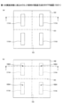
次に、第1の実施形態に係るセラミック部材100の製造方法について説明する。図2~図4は、第1の実施形態に係るセラミック部材の製造方法を示す平面図であり、図5~図6は、第1の実施形態に係るセラミック部材の製造方法を示す断面図である。図5~図6は、図2~図4中のI-I線に沿った断面図に相当する。
Next, a method for manufacturing the
先ず、図2(a)及び図5(a)に示すように、第1のグリーンシート101を準備する。第1のグリーンシート101としては、例えば、4枚のセラミック部材100が取れる大判のグリーンシートが使用される。つまり、第1のグリーンシート101は、セラミック部材100に対応する構造体が形成される4つの領域を有している。これらの領域は、後に切断線151に沿った切断により分割される。後述の第2のグリーンシート102及び第3のグリーンシート103についても同様である。次いで、第1のグリーンシート101上にアルミニウム又はアルミニウム合金のバルク状の金属膜111Aを設ける。金属膜111Aとして金属箔を用いることができる。
First, as shown in FIGS. 2(a) and 5(a), a first
その後、図2(b)及び図5(b)に示すように、金属膜111Aに到達する孔102Aが形成された第2のグリーンシート102を第1のグリーンシート101上に設ける。
Thereafter, as shown in FIGS. 2(b) and 5(b), a second
続いて、図3(a)及び図5(c)に示すように、第3のグリーンシート103を第2のグリーンシート102上に設ける。第3のグリーンシート103により孔102Aが塞がれる。本実施形態では、第2のグリーンシート102と第3のグリーンシート103との積層体が、請求項における第2のグリーンシートの一例であり、孔102Aが空隙の一例である。空隙は、第1のグリーンシート、第2のグリーンシートのどちらに形成されていてもよく、両方に形成されていてもよい。いずれの場合も、この空隙が閉塞されるように第1のグリーンシート及び第2のグリーンシートが互いに積層される。
Subsequently, as shown in FIGS. 3(a) and 5(c), a third
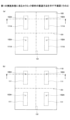
次いで、図3(b)及び図6(a)に示すように、加熱及び加圧により第1のグリーンシート101、第2のグリーンシート102及び第3のグリーンシート103を一体化する。その後、焼成を行うことにより、焼結体110を得る。この焼成の際に、金属膜111Aが溶融、凝固して導電部材111が得られる。
Next, as shown in FIGS. 3(b) and 6(a), the first
焼成によって第1のグリーンシート101、第2のグリーンシート102及び第3のグリーンシート103が略等方的に緻密化するため、焼結体110の体積は第1のグリーンシート101、第2のグリーンシート102及び第3のグリーンシート103の総体積よりも小さくなる。その一方で、導電部材111の体積はバルク状の金属膜111Aの体積と同等である。本実施形態では、第2のグリーンシート102に孔102Aが形成されており、金属膜111Aが溶融している間に、焼結体110の収縮が完了する。従って、溶融金属の一部が孔102Aに入り込んで凝固する。この結果、焼結体110の収縮に伴う内部応力の発生を避けることができる。
Because the first
焼成の後、図4(a)及び図6(b)に示すように、焼結体110の研削及び研磨を行うことで、孔102Aを露出させる。
After firing, as shown in FIGS. 4A and 6B, the
次いで、図4(b)及び図6(c)に示すように、切断線151に沿って焼結体110を切断し、個片化する。
Next, as shown in FIGS. 4(b) and 6(c), the
このようにして、第1の実施形態に係るセラミック部材100を製造することができる。
In this way, the
この製造方法によれば、一体化した第1のグリーンシート101、第2のグリーンシート102及び第3のグリーンシート103の焼成の際に、金属膜111Aから導電部材111を得ることができる。つまり、長時間の脱脂及び焼成等の、導電部材111を得るための特別な処理は必要とされない。このため、製造コストの増加を抑制することができる。また、第2のグリーンシート102に孔102Aが形成されているため、焼成に伴うセラミックの体積収縮が生じても内部応力の発生を避けることができる。
According to this manufacturing method, the
更に、従来の金属粉末のペーストを用いる方法では、導電部材に介在物が混入するが、この製造方法では、バルク状の金属膜111Aを用いることができるため、介在物の混入に伴う電気抵抗率の上昇及び熱伝導率の低減を避けることができる。
Furthermore, in the conventional method using metal powder paste, inclusions are mixed into the conductive member, but in this manufacturing method, the
第1のグリーンシート101、第2のグリーンシート102及び第3のグリーンシート103のそれぞれについて、グリーンシートを構成するセラミックのうち酸化アルミニウムの割合は、好ましくは96質量%以上であり、より好ましくは99質量%以上である。セラミックとアルミニウム又はアルミニウム合金との化学的反応を抑制するためである。
For each of the first
焼結体110を得る焼成の温度は金属膜111Aの融点以上であればよく、例えば700℃以上であることが好ましい。第1のグリーンシート101、第2のグリーンシート102及び第3のグリーンシート103の材料にもよるが、焼成温度は1300℃以上であることが好ましい。また、焼成温度が1600℃超では、溶融金属とセラミックとの間で化学的反応が生じやすくなる。このため、焼成温度は1600℃以下であることが好ましい。
The firing temperature for obtaining the
焼結体110を得る焼成の雰囲気は大気雰囲気等の酸化性雰囲気であることが好ましい。固体のアルミニウム又はアルミニウム合金の表面には不動態膜ともよばれる緻密な酸化膜が形成されている。ところが、アルミニウム又はアルミニウム合金が融点以上に加熱されると、アルミニウム又はアルミニウム合金の溶融に伴って酸化膜が破れ、真空雰囲気中又は還元性雰囲気中では、温度の上昇に伴って溶融金属の蒸発が進む。特に、1200℃以上では蒸気圧上昇が大きく、蒸発損失が大きい。これに対し、大気雰囲気等の酸化性雰囲気中では、酸化膜が破れても、速やかに新たな酸化膜が形成される。このため、アルミニウム又はアルミニウム合金の蒸発損失を抑制することができる。
The firing atmosphere for obtaining the
本実施形態では、このような酸化膜の破壊及び再形成は、主として金属膜111Aの孔102Aに露出する部分で生じ得る。酸化膜の破壊及び再形成が生じる範囲が広いほど金属の酸化損失が増加するが、本実施形態では、酸化膜の破壊及び再形成が生じる範囲が限定的であるため、アルミニウム又はアルミニウム合金の酸化損失を抑制することもできる。
In this embodiment, such destruction and reformation of the oxide film may occur mainly in the portion of the
焼成を大気雰囲気で行うことで、第1のグリーンシート101、第2のグリーンシート102及び第3のグリーンシート103に含まれる有機成分を速やかに除去することができる。有機成分の除去により、残留カーボンのセラミック特性への影響を抑制することができる。また、大気雰囲気での焼成には、水素、窒素、アンモニア分解ガス等の雰囲気制御ガスが不要である。更に、大気雰囲気には、真空雰囲気及び還元性雰囲気よりも管理が容易であり、設備コストが低いという利点もある。
By performing the firing in the air, organic components contained in the first
第1のグリーンシート101、第2のグリーンシート102及び第3のグリーンシート103の積層体から得られるセラミック部材100の数は4に限定されない。例えば、第1のグリーンシート101、第2のグリーンシート102及び第3のグリーンシート103の積層体を切断せずに、1つのセラミック部材100を製造してもよい。
The number of
最終製品のセラミック部材100において孔102Aが露出している必要はなく、セラミック部材100のユーザにて導電部材111との導通経路を形成するようにしてもよい。導電部材111との間の静電容量を用いた通信を行ってもよい。また、孔102Aが導電材料又はセラミック材料等により埋められていてもよい。
The
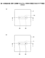
ここで、本発明者らが行った第1の実施形態に関する実験について説明する。図7~図8は、第1の実施形態に関する実験でのセラミック部材の製造方法を示す平面図である。図9~図10は、第1の実施形態に関する実験でのセラミック部材の製造方法を示す断面図である。図9~図10は、図7~図8中のI-I線に沿った断面図に相当する。 Here, an experiment related to the first embodiment conducted by the present inventors will be described. 7 and 8 are plan views showing a method for manufacturing a ceramic member in experiments related to the first embodiment. 9 to 10 are cross-sectional views showing a method for manufacturing a ceramic member in an experiment related to the first embodiment. 9 to 10 correspond to cross-sectional views taken along line II in FIGS. 7 to 8.
この実験では、先ず、図7(a)及び図9(a)に示すように、ドクターブレード法により第1のグリーンシート1を形成した。第1のグリーンシート1の形成では、平均粒径が1μm以下のアルミナ粉末と、ポリビニルブチラールと、フタル酸ジブチルと、2-プロパノールと、酢酸エチルとをボールミルにて混合したスラリーを用いた。第1のグリーンシート1の厚さは約0.5mmである。後述の第2のグリーンシート2及び第3のグリーンシート3も同様にして作製し、これらの厚さも約0.5mmである。次いで、第1のグリーンシート1上に、厚さが約0.03mmのアルミニウム箔11Aを設けた。アルミニウム箔11Aの平面形状は、30mm×10mmの矩形である。
In this experiment, first, as shown in FIGS. 7(a) and 9(a), a first green sheet 1 was formed by a doctor blade method. In forming the first green sheet 1, a slurry was used in which alumina powder having an average particle size of 1 μm or less, polyvinyl butyral, dibutyl phthalate, 2-propanol, and ethyl acetate were mixed in a ball mill. The thickness of the first green sheet 1 is approximately 0.5 mm. A second
その後、図7(b)及び図9(b)に示すように、アルミニウム箔11Aに到達する孔2Aが2箇所に形成された第2のグリーンシート2を第1のグリーンシート1上に設けた。孔の直径は3mmである。
Thereafter, as shown in FIGS. 7(b) and 9(b), a second
続いて、図8(a)及び図9(c)に示すように、第3のグリーンシート3を第2のグリーンシート2上に設け、第3のグリーンシート3により孔2Aを塞いだ。
Subsequently, as shown in FIGS. 8(a) and 9(c), a third
次いで、図10(a)に示すように、加熱及び加圧により第1のグリーンシート1、第2のグリーンシート2及び第3のグリーンシート3を一体化し、その後、大気雰囲気中で、約1500℃にて焼成を行うことにより、焼結体10を得た。この焼成の際に、アルミニウム箔11Aが溶融、凝固して導電部材11が得られた。
Next, as shown in FIG. 10(a), the first green sheet 1, the second
続いて、図8(b)及び図10(b)に示すように、焼結体10の研削及び研磨を行うことで、孔2Aを露出させた。
Subsequently, as shown in FIGS. 8(b) and 10(b), the
そして、接触抵抗を含む二端子式の簡易抵抗テスタを用いて、導電部材11の電気抵抗を測定した。導電部材11の電気抵抗は0.3mΩと十分に低かった。
Then, the electrical resistance of the
(第2の実施形態)
次に、第2の実施形態について説明する。第2の実施形態はセラミック部材を含む静電チャックに関する。図11は、第2の実施形態に係る静電チャックを示す断面図である。
(Second embodiment)
Next, a second embodiment will be described. A second embodiment relates to an electrostatic chuck that includes a ceramic member. FIG. 11 is a sectional view showing an electrostatic chuck according to the second embodiment.
図11に示すように、第2の実施形態に係る静電チャック200は、セラミックの焼結体210と、焼結体210内に設けられたアルミニウム又はアルミニウム合金の静電電極220と、焼結体210内に設けられたアルミニウム又はアルミニウム合金の静電電極230と、を有する。焼結体210の一方の面210Aに、静電電極220に到達する孔202Aと、静電電極230に到達する孔203Aと、が形成されている。孔202A内に静電電極220に接続されたビア導体221が設けられ、孔203A内に静電電極230に接続されたビア導体231が設けられている。
As shown in FIG. 11, an
このように構成された静電チャック200では、ビア導体221及び231を通じて、静電電極220又は230の一方に正の電圧が印加され、他方に負の電圧が印加される。この結果、孔202A及び203Aが形成された面210Aとは反対側の面210Bが帯電し、この面210B上に半導体ウェハ等の対象物が吸着される。
In the
静電チャック200では、静電電極220及び230の電気抵抗率を、タングステン又はモリブデンの粉末のペーストを用いて形成された静電電極の電気抵抗率よりも低くすることができる。また、静電電極220及び230の熱伝導率を、タングステン又はモリブデンの粉末のペーストを用いて形成された導電部材の熱伝導率よりも高くすることができる。
In the
更に、セラミック部材100と同様に、静電チャック200は長時間の脱脂及び焼成を行わずに製造することができ、コストの増加を抑制することができる。
Furthermore, like the
焼結体210の相対密度は、好ましくは90%以上、より好ましくは95%以上である。焼結体210の相対密度が90%未満では、連続気孔が形成される確率が高くなり、静電電極220及び230の材料であるアルミニウム又はアルミニウム合金のペネトレーションや気化損失が生じやすくなる。
The relative density of the
焼結体210はアルミニウム又はアルミニウム合金との化学的反応が進みにくい材料から構成されていることが好ましい。例えば、焼結体210は、96質量%以上の酸化アルミニウムを含んでいることが好ましく、99質量%以上の酸化アルミニウムを含んでいることがより好ましい。
It is preferable that the
静電チャック200の製造に当たっては、例えば、セラミック部材100の製造方法に倣う方法により、孔202A及び203Aを露出させる焼結体210の研削及び研磨までの処理を行い、その後に、孔202A内にビア導体221を形成し、孔203A内にビア導体231を形成することができる。
In manufacturing the
孔202A及び203Aのサイズによっては、セラミックの体積収縮で孔202A及び203Aに入り込んで凝固したアルミニウム又はアルミニウム合金をビア導体221及び231として用いることもできる。
Depending on the size of the
(第3の実施形態)
次に、第3の実施形態について説明する。第3の実施形態はセラミック部材を含むインダクタに関する。図12は、第3の実施形態に係るインダクタを示す平面図である。
(Third embodiment)
Next, a third embodiment will be described. A third embodiment relates to an inductor including a ceramic member. FIG. 12 is a plan view showing an inductor according to the third embodiment.
図12に示すように、第3の実施形態に係るインダクタ300は、セラミックの焼結体310と、焼結体310内に設けられたアルミニウム又はアルミニウム合金の導電部材311と、を有する。導電部材311の平面形状は螺旋状となっている。焼結体310の一方の面に、導電部材311の一端に到達する孔302Aと、導電部材311の他端に到達する孔302Bと、が形成されている。
As shown in FIG. 12, an
このように構成されたインダクタ300は、孔302A及び302Bを通じて外部の回路に電気的に接続することができる。
The
インダクタ300では、導電部材311の電気抵抗率を、タングステン又はモリブデンの粉末のペーストを用いて形成された静電電極の電気抵抗率よりも低くすることができる。また、導電部材311の熱伝導率を、タングステン又はモリブデンの粉末のペーストを用いて形成された導電部材の熱伝導率よりも高くすることができる。
In the
更に、セラミック部材100と同様に、インダクタ300は長時間の脱脂及び焼成を行わずに製造することができ、コストの増加を抑制することができる。
Furthermore, like the
焼結体310の相対密度は、好ましくは90%以上、より好ましくは95%以上である。焼結体310の相対密度が90%未満では、連続気孔が形成される確率が高くなり、導電部材311の材料であるアルミニウム又はアルミニウム合金のペネトレーションや気化損失が生じやすくなる。
The relative density of the
焼結体310はアルミニウム又はアルミニウム合金との化学的反応が進みにくい材料から構成されていることが好ましい。例えば、焼結体210は、96質量%以上の酸化アルミニウムを含んでいることが好ましく、99質量%以上の酸化アルミニウムを含んでいることがより好ましい。
It is preferable that the
インダクタ300の製造に当たっては、例えば、セラミック部材100の製造方法に倣う方法により、孔302A及び302Bを露出させる焼結体310の研削及び研磨までの処理を行うことができる。
In manufacturing the
以上、好ましい実施の形態等について詳説したが、上述した実施の形態等に制限されることはなく、特許請求の範囲に記載された範囲を逸脱することなく、上述した実施の形態等に種々の変形及び置換を加えることができる。 Although the preferred embodiments have been described in detail above, they are not limited to the embodiments described above, and various modifications may be made to the embodiments described above without departing from the scope of the claims. Variations and substitutions can be made.
例えば、第2の実施形態では、セラミック部材を静電チャックに応用し、第三の実施形態では、セラミック部材をインダクタに応用しているが、セラミック部材の用途は限定されない。例えば、セラミック部材をパワー半導体装置等の実装基板に用いてもよい。 For example, in the second embodiment, the ceramic member is applied to an electrostatic chuck, and in the third embodiment, the ceramic member is applied to an inductor, but the use of the ceramic member is not limited. For example, a ceramic member may be used for a mounting board for a power semiconductor device or the like.
1、101 第1のグリーンシート
2、102 第2のグリーンシート
2A、102A 孔
3、103 第3のグリーンシート
10、110 焼結体
11、111 導電部材
11A アルミニウム箔
111A 金属膜
200 静電チャック
300 インダクタ
1, 101 First
Claims (6)
前記金属膜の融点以上の温度で前記第1のグリーンシート及び前記第2のグリーンシートの焼成を行ってセラミックの焼結体を得る工程と、
を有し、
前記第1のグリーンシートを構成するセラミックのうち96質量%以上が酸化アルミニウムであり、
前記第2のグリーンシートを構成するセラミックのうち96質量%以上が酸化アルミニウムであり、
前記焼結体を構成するセラミックのうち96質量%以上が酸化アルミニウムであり、
前記焼結体の相対密度が90%以上であり、
前記第1のグリーンシート若しくは前記第2のグリーンシート又はこれらの両方の前記金属膜と接する面の一部に空隙が設けられており、
前記焼結体を得る工程において、溶融した前記金属膜の一部が前記空隙に入り込んで凝固することを特徴とするセラミック部材の製造方法。 sandwiching a metal film of aluminum or aluminum alloy between a first green sheet and a second green sheet;
firing the first green sheet and the second green sheet at a temperature equal to or higher than the melting point of the metal film to obtain a ceramic sintered body;
has
96% by mass or more of the ceramic constituting the first green sheet is aluminum oxide,
96% by mass or more of the ceramic constituting the second green sheet is aluminum oxide,
96% by mass or more of the ceramic constituting the sintered body is aluminum oxide,
The relative density of the sintered body is 90% or more,
A void is provided in a part of the surface of the first green sheet, the second green sheet, or both of them that is in contact with the metal film,
A method for manufacturing a ceramic member, characterized in that in the step of obtaining the sintered body, a part of the molten metal film enters the void and solidifies .
Priority Applications (5)
| Application Number | Priority Date | Filing Date | Title |
|---|---|---|---|
| JP2019006355A JP7378210B2 (en) | 2019-01-17 | 2019-01-17 | Ceramic component manufacturing method |
| TW108148341A TW202045456A (en) | 2019-01-17 | 2019-12-30 | Ceramic member and method for manufacturing same |
| CN202010004322.9A CN111446196A (en) | 2019-01-17 | 2020-01-03 | Ceramic member and method for manufacturing same |
| US16/735,859 US11370709B2 (en) | 2019-01-17 | 2020-01-07 | Ceramic member |
| KR1020200003044A KR20200089614A (en) | 2019-01-17 | 2020-01-09 | Ceramic member |
Applications Claiming Priority (1)
| Application Number | Priority Date | Filing Date | Title |
|---|---|---|---|
| JP2019006355A JP7378210B2 (en) | 2019-01-17 | 2019-01-17 | Ceramic component manufacturing method |
Publications (3)
| Publication Number | Publication Date |
|---|---|
| JP2020114789A JP2020114789A (en) | 2020-07-30 |
| JP2020114789A5 JP2020114789A5 (en) | 2022-01-06 |
| JP7378210B2 true JP7378210B2 (en) | 2023-11-13 |
Family
ID=71609715
Family Applications (1)
| Application Number | Title | Priority Date | Filing Date |
|---|---|---|---|
| JP2019006355A Active JP7378210B2 (en) | 2019-01-17 | 2019-01-17 | Ceramic component manufacturing method |
Country Status (5)
| Country | Link |
|---|---|
| US (1) | US11370709B2 (en) |
| JP (1) | JP7378210B2 (en) |
| KR (1) | KR20200089614A (en) |
| CN (1) | CN111446196A (en) |
| TW (1) | TW202045456A (en) |
Families Citing this family (2)
| Publication number | Priority date | Publication date | Assignee | Title |
|---|---|---|---|---|
| US11177152B2 (en) * | 2018-09-05 | 2021-11-16 | Shinko Electric Industries Co., Ltd. | Ceramic substrate containing aluminum oxide and electrostatic chuck having electrode containing tungsten with oxides |
| CN114702331B (en) * | 2022-05-06 | 2023-03-24 | 常州恒立气动科技有限公司 | Ceramic sintered part, preparation method and bottle mouth valve assembly |
Citations (10)
| Publication number | Priority date | Publication date | Assignee | Title |
|---|---|---|---|---|
| JP2000031254A (en) | 1998-07-07 | 2000-01-28 | Shin Etsu Chem Co Ltd | Ceramic electrostatic chuck and manufacture thereof |
| JP2002121078A (en) | 2000-10-10 | 2002-04-23 | Sumitomo Metal Electronics Devices Inc | Method of producing sintered compact |
| JP2002322521A (en) | 2001-04-25 | 2002-11-08 | Taiheiyo Cement Corp | Method for producing metal-ceramic composite material with embedded heater |
| JP2004238218A (en) | 2003-02-03 | 2004-08-26 | Taiheiyo Cement Corp | Ceramic joint body |
| JP2005012143A (en) | 2003-06-23 | 2005-01-13 | Kyocera Corp | Wafer holding member |
| JP2005223185A (en) | 2004-02-06 | 2005-08-18 | Toto Ltd | Electrostatic chuck and its manufacturing method |
| JP2014011251A (en) | 2012-06-28 | 2014-01-20 | Taiheiyo Cement Corp | Manufacturing method of electrostatic chuck |
| JP2017218352A (en) | 2016-06-09 | 2017-12-14 | 新光電気工業株式会社 | Sintered body, manufacturing method therefor and electrostatic chuck |
| JP2018142589A (en) | 2017-02-27 | 2018-09-13 | 新光電気工業株式会社 | Substrate fixture and substrate fixing device |
| JP2018537002A (en) | 2015-11-02 | 2018-12-13 | コンポーネント リ−エンジニアリング カンパニー インコーポレイテッド | Electrostatic chuck for clamping in high temperature semiconductor processing and method of manufacturing the same |
Family Cites Families (11)
| Publication number | Priority date | Publication date | Assignee | Title |
|---|---|---|---|---|
| JPS62260373A (en) * | 1986-05-06 | 1987-11-12 | Omron Tateisi Electronics Co | Manufacture of laminated type piezoelectric actuator |
| JPS63253656A (en) * | 1987-04-10 | 1988-10-20 | Sumitomo Electric Ind Ltd | Semiconductor device |
| JP3057932B2 (en) * | 1992-10-01 | 2000-07-04 | 三菱マテリアル株式会社 | Joining method of ceramic sintered body |
| JPH0715101A (en) * | 1993-06-25 | 1995-01-17 | Shinko Electric Ind Co Ltd | Oxide ceramic circuit board and its manufacture |
| JPH07245482A (en) * | 1994-03-03 | 1995-09-19 | Shinko Electric Ind Co Ltd | Ceramic circuit board and its manufacture |
| JP3483012B2 (en) * | 1994-07-01 | 2004-01-06 | 新光電気工業株式会社 | Sintered body for producing ceramic substrate, ceramic substrate and method for producing the same |
| JP3767719B2 (en) * | 1997-10-30 | 2006-04-19 | 信越化学工業株式会社 | Electrostatic chuck |
| JP2007254181A (en) * | 2006-03-22 | 2007-10-04 | Denki Kagaku Kogyo Kk | Ceramic sintered compact, method of manufacturing the same and exothermic element for vaporization of metal |
| WO2011090133A1 (en) * | 2010-01-20 | 2011-07-28 | 古河電気工業株式会社 | Composite electric cable and process for producing same |
| JP2013070026A (en) * | 2011-09-08 | 2013-04-18 | Rohm Co Ltd | Semiconductor device, manufacturing method of semiconductor device, mounting structure of semiconductor device, and power semiconductor device |
| CN105934803B (en) * | 2016-04-29 | 2018-02-02 | 深圳顺络电子股份有限公司 | Compound wire and preparation method thereof and a kind of preparation method of power inductance |
-
2019
- 2019-01-17 JP JP2019006355A patent/JP7378210B2/en active Active
- 2019-12-30 TW TW108148341A patent/TW202045456A/en unknown
-
2020
- 2020-01-03 CN CN202010004322.9A patent/CN111446196A/en active Pending
- 2020-01-07 US US16/735,859 patent/US11370709B2/en active Active
- 2020-01-09 KR KR1020200003044A patent/KR20200089614A/en unknown
Patent Citations (10)
| Publication number | Priority date | Publication date | Assignee | Title |
|---|---|---|---|---|
| JP2000031254A (en) | 1998-07-07 | 2000-01-28 | Shin Etsu Chem Co Ltd | Ceramic electrostatic chuck and manufacture thereof |
| JP2002121078A (en) | 2000-10-10 | 2002-04-23 | Sumitomo Metal Electronics Devices Inc | Method of producing sintered compact |
| JP2002322521A (en) | 2001-04-25 | 2002-11-08 | Taiheiyo Cement Corp | Method for producing metal-ceramic composite material with embedded heater |
| JP2004238218A (en) | 2003-02-03 | 2004-08-26 | Taiheiyo Cement Corp | Ceramic joint body |
| JP2005012143A (en) | 2003-06-23 | 2005-01-13 | Kyocera Corp | Wafer holding member |
| JP2005223185A (en) | 2004-02-06 | 2005-08-18 | Toto Ltd | Electrostatic chuck and its manufacturing method |
| JP2014011251A (en) | 2012-06-28 | 2014-01-20 | Taiheiyo Cement Corp | Manufacturing method of electrostatic chuck |
| JP2018537002A (en) | 2015-11-02 | 2018-12-13 | コンポーネント リ−エンジニアリング カンパニー インコーポレイテッド | Electrostatic chuck for clamping in high temperature semiconductor processing and method of manufacturing the same |
| JP2017218352A (en) | 2016-06-09 | 2017-12-14 | 新光電気工業株式会社 | Sintered body, manufacturing method therefor and electrostatic chuck |
| JP2018142589A (en) | 2017-02-27 | 2018-09-13 | 新光電気工業株式会社 | Substrate fixture and substrate fixing device |
Also Published As
| Publication number | Publication date |
|---|---|
| TW202045456A (en) | 2020-12-16 |
| JP2020114789A (en) | 2020-07-30 |
| KR20200089614A (en) | 2020-07-27 |
| US20200231505A1 (en) | 2020-07-23 |
| CN111446196A (en) | 2020-07-24 |
| US11370709B2 (en) | 2022-06-28 |
Similar Documents
| Publication | Publication Date | Title |
|---|---|---|
| JP5117146B2 (en) | Heating device | |
| JP5012899B2 (en) | Multilayer ceramic substrate and manufacturing method thereof | |
| JP7378210B2 (en) | Ceramic component manufacturing method | |
| JP7306915B2 (en) | Ceramic substrate, electrostatic chuck, manufacturing method of electrostatic chuck | |
| JP2010177482A (en) | Wiring board with metal member and connection method thereof | |
| JP2008004733A (en) | Manufacturing method of ceramic substrate | |
| JP7309666B2 (en) | Multilayer ceramic substrate and electronic device | |
| US6629367B2 (en) | Electrically isolated via in a multilayer ceramic package | |
| JP7366551B2 (en) | Composite green sheet, ceramic member, method for manufacturing composite green sheet, and method for manufacturing ceramic member | |
| JP3955389B2 (en) | Capacitor-embedded substrate and manufacturing method thereof | |
| JP2019523545A (en) | Multilayer device and method for manufacturing the multilayer device | |
| EP3457434B1 (en) | Method for producing a semiconductor substrate for a power semiconductor module arrangement | |
| JP5284227B2 (en) | Electrostatic chuck and method for manufacturing electrostatic chuck | |
| JP2003017552A (en) | Ceramic heater, and electrostatic chuck incorporating same | |
| JP2005093846A (en) | Method for manufacturing multilayer ceramic substrate and multilayer ceramic substrate | |
| WO2008075504A1 (en) | Method for manufacturing thin-layer capacitor, thin-layer capacitor, and method for manufacturing wiring board with built-in capacitor | |
| US10389105B2 (en) | Overvoltage protection element and method for producing an overvoltage protection element | |
| KR102039802B1 (en) | Ceramic body for electrostatic chuck | |
| JP6054696B2 (en) | Electrostatic chuck | |
| KR100497953B1 (en) | conductive ceramic electrode and including a electrostatic chuck | |
| WO2021065544A1 (en) | Structure and heating device | |
| JP6455633B2 (en) | Multilayer ceramic substrate and electronic device | |
| JP2004200614A (en) | Wiring board | |
| JP4396110B2 (en) | Manufacturing method of multilayer ceramic electronic component | |
| WO2017195414A1 (en) | Ceramic electronic component and method for manufacturing ceramic electronic component |
Legal Events
| Date | Code | Title | Description |
|---|---|---|---|
| A521 | Request for written amendment filed |
Free format text: JAPANESE INTERMEDIATE CODE: A523 Effective date: 20211129 |
|
| A621 | Written request for application examination |
Free format text: JAPANESE INTERMEDIATE CODE: A621 Effective date: 20211129 |
|
| A977 | Report on retrieval |
Free format text: JAPANESE INTERMEDIATE CODE: A971007 Effective date: 20221117 |
|
| A131 | Notification of reasons for refusal |
Free format text: JAPANESE INTERMEDIATE CODE: A131 Effective date: 20230104 |
|
| A521 | Request for written amendment filed |
Free format text: JAPANESE INTERMEDIATE CODE: A523 Effective date: 20230303 |
|
| A131 | Notification of reasons for refusal |
Free format text: JAPANESE INTERMEDIATE CODE: A131 Effective date: 20230606 |
|
| A521 | Request for written amendment filed |
Free format text: JAPANESE INTERMEDIATE CODE: A523 Effective date: 20230802 |
|
| TRDD | Decision of grant or rejection written | ||
| A01 | Written decision to grant a patent or to grant a registration (utility model) |
Free format text: JAPANESE INTERMEDIATE CODE: A01 Effective date: 20231024 |
|
| A61 | First payment of annual fees (during grant procedure) |
Free format text: JAPANESE INTERMEDIATE CODE: A61 Effective date: 20231031 |
|
| R150 | Certificate of patent or registration of utility model |
Ref document number: 7378210 Country of ref document: JP Free format text: JAPANESE INTERMEDIATE CODE: R150 |