JP7369953B2 - switching circuit - Google Patents
switching circuit Download PDFInfo
- Publication number
- JP7369953B2 JP7369953B2 JP2020502843A JP2020502843A JP7369953B2 JP 7369953 B2 JP7369953 B2 JP 7369953B2 JP 2020502843 A JP2020502843 A JP 2020502843A JP 2020502843 A JP2020502843 A JP 2020502843A JP 7369953 B2 JP7369953 B2 JP 7369953B2
- Authority
- JP
- Japan
- Prior art keywords
- terminal
- gate
- switching element
- switching
- source
- Prior art date
- Legal status (The legal status is an assumption and is not a legal conclusion. Google has not performed a legal analysis and makes no representation as to the accuracy of the status listed.)
- Active
Links
- 239000003990 capacitor Substances 0.000 claims description 80
- 239000004065 semiconductor Substances 0.000 claims description 13
- 230000005669 field effect Effects 0.000 claims description 10
- 150000004767 nitrides Chemical class 0.000 claims description 9
- 230000004048 modification Effects 0.000 description 70
- 238000012986 modification Methods 0.000 description 70
- 238000010586 diagram Methods 0.000 description 21
- 238000010304 firing Methods 0.000 description 19
- 229910002601 GaN Inorganic materials 0.000 description 11
- JMASRVWKEDWRBT-UHFFFAOYSA-N Gallium nitride Chemical compound [Ga]#N JMASRVWKEDWRBT-UHFFFAOYSA-N 0.000 description 11
- 230000007423 decrease Effects 0.000 description 11
- 238000005516 engineering process Methods 0.000 description 10
- 230000001965 increasing effect Effects 0.000 description 10
- 230000007274 generation of a signal involved in cell-cell signaling Effects 0.000 description 9
- 230000001939 inductive effect Effects 0.000 description 8
- 230000003071 parasitic effect Effects 0.000 description 8
- 230000015556 catabolic process Effects 0.000 description 5
- 238000000034 method Methods 0.000 description 5
- 238000010992 reflux Methods 0.000 description 5
- 238000007599 discharging Methods 0.000 description 4
- 239000000470 constituent Substances 0.000 description 3
- 230000000694 effects Effects 0.000 description 3
- 230000007257 malfunction Effects 0.000 description 3
- 230000010355 oscillation Effects 0.000 description 3
- 230000000630 rising effect Effects 0.000 description 3
- 150000001875 compounds Chemical class 0.000 description 2
- 230000003247 decreasing effect Effects 0.000 description 2
- 238000002347 injection Methods 0.000 description 2
- 239000007924 injection Substances 0.000 description 2
- 239000000919 ceramic Substances 0.000 description 1
- 230000006866 deterioration Effects 0.000 description 1
- 239000000463 material Substances 0.000 description 1
- 239000011347 resin Substances 0.000 description 1
- 229920005989 resin Polymers 0.000 description 1
- 239000003566 sealing material Substances 0.000 description 1
- 239000000243 solution Substances 0.000 description 1
Images


Classifications
-
- H—ELECTRICITY
- H03—ELECTRONIC CIRCUITRY
- H03K—PULSE TECHNIQUE
- H03K17/00—Electronic switching or gating, i.e. not by contact-making and –breaking
- H03K17/51—Electronic switching or gating, i.e. not by contact-making and –breaking characterised by the components used
- H03K17/56—Electronic switching or gating, i.e. not by contact-making and –breaking characterised by the components used by the use, as active elements, of semiconductor devices
- H03K17/687—Electronic switching or gating, i.e. not by contact-making and –breaking characterised by the components used by the use, as active elements, of semiconductor devices the devices being field-effect transistors
-
- H—ELECTRICITY
- H03—ELECTRONIC CIRCUITRY
- H03K—PULSE TECHNIQUE
- H03K17/00—Electronic switching or gating, i.e. not by contact-making and –breaking
- H03K17/08—Modifications for protecting switching circuit against overcurrent or overvoltage
- H03K17/081—Modifications for protecting switching circuit against overcurrent or overvoltage without feedback from the output circuit to the control circuit
- H03K17/0812—Modifications for protecting switching circuit against overcurrent or overvoltage without feedback from the output circuit to the control circuit by measures taken in the control circuit
- H03K17/08122—Modifications for protecting switching circuit against overcurrent or overvoltage without feedback from the output circuit to the control circuit by measures taken in the control circuit in field-effect transistor switches
-
- H—ELECTRICITY
- H02—GENERATION; CONVERSION OR DISTRIBUTION OF ELECTRIC POWER
- H02M—APPARATUS FOR CONVERSION BETWEEN AC AND AC, BETWEEN AC AND DC, OR BETWEEN DC AND DC, AND FOR USE WITH MAINS OR SIMILAR POWER SUPPLY SYSTEMS; CONVERSION OF DC OR AC INPUT POWER INTO SURGE OUTPUT POWER; CONTROL OR REGULATION THEREOF
- H02M1/00—Details of apparatus for conversion
- H02M1/08—Circuits specially adapted for the generation of control voltages for semiconductor devices incorporated in static converters
-
- H—ELECTRICITY
- H02—GENERATION; CONVERSION OR DISTRIBUTION OF ELECTRIC POWER
- H02M—APPARATUS FOR CONVERSION BETWEEN AC AND AC, BETWEEN AC AND DC, OR BETWEEN DC AND DC, AND FOR USE WITH MAINS OR SIMILAR POWER SUPPLY SYSTEMS; CONVERSION OF DC OR AC INPUT POWER INTO SURGE OUTPUT POWER; CONTROL OR REGULATION THEREOF
- H02M1/00—Details of apparatus for conversion
- H02M1/32—Means for protecting converters other than automatic disconnection
- H02M1/34—Snubber circuits
-
- H—ELECTRICITY
- H03—ELECTRONIC CIRCUITRY
- H03K—PULSE TECHNIQUE
- H03K17/00—Electronic switching or gating, i.e. not by contact-making and –breaking
- H03K17/04—Modifications for accelerating switching
- H03K17/041—Modifications for accelerating switching without feedback from the output circuit to the control circuit
- H03K17/0412—Modifications for accelerating switching without feedback from the output circuit to the control circuit by measures taken in the control circuit
- H03K17/04123—Modifications for accelerating switching without feedback from the output circuit to the control circuit by measures taken in the control circuit in field-effect transistor switches
-
- H—ELECTRICITY
- H03—ELECTRONIC CIRCUITRY
- H03K—PULSE TECHNIQUE
- H03K17/00—Electronic switching or gating, i.e. not by contact-making and –breaking
- H03K17/51—Electronic switching or gating, i.e. not by contact-making and –breaking characterised by the components used
- H03K17/56—Electronic switching or gating, i.e. not by contact-making and –breaking characterised by the components used by the use, as active elements, of semiconductor devices
- H03K17/687—Electronic switching or gating, i.e. not by contact-making and –breaking characterised by the components used by the use, as active elements, of semiconductor devices the devices being field-effect transistors
- H03K17/6877—Electronic switching or gating, i.e. not by contact-making and –breaking characterised by the components used by the use, as active elements, of semiconductor devices the devices being field-effect transistors the control circuit comprising active elements different from those used in the output circuit
-
- H—ELECTRICITY
- H03—ELECTRONIC CIRCUITRY
- H03K—PULSE TECHNIQUE
- H03K17/00—Electronic switching or gating, i.e. not by contact-making and –breaking
- H03K17/51—Electronic switching or gating, i.e. not by contact-making and –breaking characterised by the components used
- H03K17/74—Electronic switching or gating, i.e. not by contact-making and –breaking characterised by the components used by the use, as active elements, of diodes
-
- H—ELECTRICITY
- H02—GENERATION; CONVERSION OR DISTRIBUTION OF ELECTRIC POWER
- H02M—APPARATUS FOR CONVERSION BETWEEN AC AND AC, BETWEEN AC AND DC, OR BETWEEN DC AND DC, AND FOR USE WITH MAINS OR SIMILAR POWER SUPPLY SYSTEMS; CONVERSION OF DC OR AC INPUT POWER INTO SURGE OUTPUT POWER; CONTROL OR REGULATION THEREOF
- H02M7/00—Conversion of ac power input into dc power output; Conversion of dc power input into ac power output
- H02M7/003—Constructional details, e.g. physical layout, assembly, wiring or busbar connections
-
- H—ELECTRICITY
- H02—GENERATION; CONVERSION OR DISTRIBUTION OF ELECTRIC POWER
- H02M—APPARATUS FOR CONVERSION BETWEEN AC AND AC, BETWEEN AC AND DC, OR BETWEEN DC AND DC, AND FOR USE WITH MAINS OR SIMILAR POWER SUPPLY SYSTEMS; CONVERSION OF DC OR AC INPUT POWER INTO SURGE OUTPUT POWER; CONTROL OR REGULATION THEREOF
- H02M7/00—Conversion of ac power input into dc power output; Conversion of dc power input into ac power output
- H02M7/42—Conversion of dc power input into ac power output without possibility of reversal
- H02M7/44—Conversion of dc power input into ac power output without possibility of reversal by static converters
- H02M7/48—Conversion of dc power input into ac power output without possibility of reversal by static converters using discharge tubes with control electrode or semiconductor devices with control electrode
- H02M7/53—Conversion of dc power input into ac power output without possibility of reversal by static converters using discharge tubes with control electrode or semiconductor devices with control electrode using devices of a triode or transistor type requiring continuous application of a control signal
- H02M7/537—Conversion of dc power input into ac power output without possibility of reversal by static converters using discharge tubes with control electrode or semiconductor devices with control electrode using devices of a triode or transistor type requiring continuous application of a control signal using semiconductor devices only, e.g. single switched pulse inverters
- H02M7/538—Conversion of dc power input into ac power output without possibility of reversal by static converters using discharge tubes with control electrode or semiconductor devices with control electrode using devices of a triode or transistor type requiring continuous application of a control signal using semiconductor devices only, e.g. single switched pulse inverters in a push-pull configuration
-
- H—ELECTRICITY
- H03—ELECTRONIC CIRCUITRY
- H03K—PULSE TECHNIQUE
- H03K2217/00—Indexing scheme related to electronic switching or gating, i.e. not by contact-making or -breaking covered by H03K17/00
- H03K2217/0036—Means reducing energy consumption
-
- Y—GENERAL TAGGING OF NEW TECHNOLOGICAL DEVELOPMENTS; GENERAL TAGGING OF CROSS-SECTIONAL TECHNOLOGIES SPANNING OVER SEVERAL SECTIONS OF THE IPC; TECHNICAL SUBJECTS COVERED BY FORMER USPC CROSS-REFERENCE ART COLLECTIONS [XRACs] AND DIGESTS
- Y02—TECHNOLOGIES OR APPLICATIONS FOR MITIGATION OR ADAPTATION AGAINST CLIMATE CHANGE
- Y02B—CLIMATE CHANGE MITIGATION TECHNOLOGIES RELATED TO BUILDINGS, e.g. HOUSING, HOUSE APPLIANCES OR RELATED END-USER APPLICATIONS
- Y02B70/00—Technologies for an efficient end-user side electric power management and consumption
- Y02B70/10—Technologies improving the efficiency by using switched-mode power supplies [SMPS], i.e. efficient power electronics conversion e.g. power factor correction or reduction of losses in power supplies or efficient standby modes
Description
本発明は、スイッチング素子を駆動するスイッチング回路に関し、特に、ノーマリオフ型の接合型電界効果トランジスタをスイッチング素子として駆動する回路に関する。 The present invention relates to a switching circuit that drives a switching element, and particularly to a circuit that drives a normally-off junction field effect transistor as a switching element.
スイッチング電源やインバータ等の機器では、スイッチング素子が用いられ、スイッチング素子のスイッチング周波数を上げることで、コンデンサやトランス等の回路部品を小型化できる。近年、このような高周波用途のスイッチング素子として、GaNトランジスタに代表される、ワイドバンドギャップ型の化合物半導体を利用したノーマリオフ型の接合型電界効果トランジスタが注目されている。 Switching elements are used in devices such as switching power supplies and inverters, and by increasing the switching frequency of the switching elements, circuit components such as capacitors and transformers can be made smaller. In recent years, normally-off junction field effect transistors using wide bandgap compound semiconductors, typified by GaN transistors, have been attracting attention as switching elements for such high frequency applications.
そこで、従来、スイッチング素子としてノーマリオフ型の接合型電界効果トランジスタを駆動するスイッチング回路についての様々な技術が提案されている(例えば、特許文献1、2参照)。なお、スイッチング回路による駆動の対象となるトランジスタを、以下、単に「スイッチング素子」ともいう。
Therefore, various techniques have been proposed for switching circuits that drive normally-off type junction field effect transistors as switching elements (see, for example,
特許文献1の技術では、スイッチング素子を駆動する駆動回路として、駆動信号発生回路を構成する第1スイッチ素子及び第2スイッチ素子それぞれの出力端子とスイッチング素子のゲート端子との間に複数の抵抗器及び一つのコンデンサを接続した回路が開示されている。これにより、スイッチング素子のゲート充電電流及び放電電流を個別かつ最適に調整できるとともに、スイッチング素子のターンオン時及びターンオフ時の誤動作を防ぐことが可能になる。なお、以降では、スイッチング素子のターンオン及びターンオフを、それぞれ、単に、「ターンオン」及び「ターンオフ」ともいう。
In the technology of
また、特許文献2の技術では、スイッチング素子を駆動する駆動回路として、駆動信号発生回路とスイッチング素子のゲート端子との間にコンデンサが接続され、さらに、スイッチング素子のゲート端子とソース端子との間に、整流素子及びツェナーダイオードで構成される逆バイアス電圧生成回路が接続された回路が開示されている。これにより、ターンオフ動作が高速化される。 Furthermore, in the technology of Patent Document 2, a capacitor is connected between the drive signal generation circuit and the gate terminal of the switching element as a drive circuit that drives the switching element, and further, a capacitor is connected between the gate terminal and the source terminal of the switching element. discloses a circuit to which a reverse bias voltage generation circuit composed of a rectifying element and a Zener diode is connected. This speeds up the turn-off operation.
しかしながら、特許文献1の技術では、ターンオフ時にスイッチング素子のゲート・ソース間に過剰の負バイアスが与えられ、スイッチング素子に対するゲート耐圧不良が発生したり、還流動作時のロス(つまり、電力損失)が大きくなったりするという問題がある。ここで、還流動作とは、スイッチング素子に接続された誘導性負荷に流れる電流が遮断されたときに、スイッチング素子を介して誘導性負荷に電流を流し続けようとする動作をいう。
However, with the technology of
また、特許文献1の技術では、ターンオン時にスイッチング素子のゲート端子に充電された電荷を短時間で放電するために、第1スイッチ素子の出力端子とスイッチング素子のゲート端子との間に接続された抵抗器の抵抗値を小さくする必要があるが、これらの抵抗値を過剰に小さくするとスイッチング素子のゲート電圧が耐圧を超えたり、駆動ロスが大きくなったりするなどの課題が生じるために、その抵抗値を小さくするには限度がある。そのために、スイッチング素子に期待される高周波動作に限界があるという問題がある。
Further, in the technology of
また、特許文献2の技術では、スイッチング素子のゲート電極がオーミック接合のタイプである場合、ターンオン時に、ゲート・ソース間電圧が2.5~3Vであったとしてもゲート・ソース間に数mA~数10mA程度の電流が流れるため、ゲート・ソース間電圧が減少し、ターンオン状態を維持できないという問題がある。 In addition, in the technology of Patent Document 2, if the gate electrode of the switching element is an ohmic junction type, even if the gate-source voltage is 2.5 to 3V at turn-on, the voltage between the gate and source is several mA to Since a current of about several tens of milliamperes flows, there is a problem that the voltage between the gate and the source decreases, making it impossible to maintain the turned-on state.
また、特許文献2の技術では、スイッチング素子がターンオフ状態であるときに、誘導性負荷等に起因してソース電位を基準としてドレイン電圧が上昇した場合には、ドレイン・ゲート間の寄生容量への充電電流が、駆動信号発生回路とスイッチング素子のゲート端子との間に接続されたコンデンサにも流れるため、コンデンサが再放電され、ゲート・ソース間電位が増加し、その増加したゲート・ソース間電位がスイッチング素子の閾値を越えた場合には、誤点弧を起こす可能性がある。なお、誤点弧とは、スイッチング素子が誤ってターンオンすることをいう。 Furthermore, in the technology of Patent Document 2, when the switching element is in the turn-off state, if the drain voltage increases with respect to the source potential due to an inductive load, etc., the parasitic capacitance between the drain and gate increases. Since the charging current also flows to the capacitor connected between the drive signal generation circuit and the gate terminal of the switching element, the capacitor is discharged again and the gate-source potential increases, and the increased gate-source potential If exceeds the threshold of the switching element, false ignition may occur. Incidentally, erroneous ignition means that a switching element is erroneously turned on.
そこで、本発明は、上記問題点に鑑みてなされたものであり、スイッチング素子を駆動するスイッチング回路であって、スイッチング素子に対するゲート耐圧不良の発生を抑制し、還流動作時のロスを抑制し、スイッチング素子の高周波動作の限界を緩和し、ターンオン時の導通状態をより確実に維持し、かつ、誤点弧の発生を抑制することができるスイッチング回路を提供することを目的とする。 The present invention has been made in view of the above-mentioned problems, and is a switching circuit for driving a switching element, which suppresses the occurrence of a gate withstand voltage failure in the switching element, suppresses loss during freewheeling operation, It is an object of the present invention to provide a switching circuit that can alleviate the limitations of high-frequency operation of a switching element, more reliably maintain a conductive state when turned on, and suppress the occurrence of erroneous firing.
上記目的を達成するために、本発明の一形態に係るスイッチング回路は、ソース端子、ドレイン端子及びゲート端子を有するノーマリオフ型の接合型電界効果トランジスタと、第1の電源入力端子、前記第1の電源入力端子の電位又はハイインピーダンス状態を出力する第1の出力端子、第2の電源入力端子、前記第2の電源入力端子の電位又はハイインピーダンス状態を出力する第2の出力端子、及び、前記第1の出力端子が前記第1の電源入力端子の電位を出力し、かつ、前記第2の出力端子がハイインピーダンス状態を出力する第1の出力状態と、前記第1の出力端子がハイインピーダンス状態を出力し、かつ、前記第2の出力端子が前記第2の電源入力端子の電位を出力する第2の出力状態とを切り替えるための入力端子を有する駆動部と、前記ソース端子と前記ゲート端子との間に接続され、前記ソース端子側に陽極を有し、前記ゲート端子側に陰極を有する第1の整流素子と、前記第1の出力端子と前記ゲート端子との間に接続された第1の抵抗器と、前記第1の抵抗器と並列に接続された直列回路であって、直列に接続されたコンデンサと第2の抵抗器とを有する直列回路と、前記ゲート端子側に陽極を有し、前記第2の出力端子側に陰極を有する第2の整流素子とを備え、前記ソース端子は、前記第2の電源入力端子と接続され、前記第2の整流素子は、直列に接続された前記コンデンサ及び前記第2の抵抗器のうちの少なくとも前記コンデンサと並列に接続されており、前記コンデンサは、前記ゲート端子側に接続され、前記第2の抵抗器は、前記第1の出力端子側に接続されている。 In order to achieve the above object, a switching circuit according to one embodiment of the present invention includes a normally-off junction field effect transistor having a source terminal, a drain terminal, and a gate terminal, a first power input terminal, and the first power supply input terminal. a first output terminal that outputs the potential or high impedance state of the power input terminal, a second power input terminal, a second output terminal that outputs the potential or high impedance state of the second power input terminal, and the a first output state in which the first output terminal outputs the potential of the first power supply input terminal and the second output terminal outputs a high impedance state; a drive unit having an input terminal for outputting a state and switching between a second output state in which the second output terminal outputs a potential of the second power supply input terminal; the source terminal and the gate; a first rectifying element connected between the first output terminal and the gate terminal, the first rectifying element having an anode on the source terminal side and a cathode on the gate terminal side; a first resistor; a series circuit connected in parallel with the first resistor, the series circuit having a capacitor and a second resistor connected in series; and an anode on the gate terminal side. and a second rectifying element having a cathode on the second output terminal side, the source terminal is connected to the second power input terminal, and the second rectifying element is connected in series. Of the connected capacitor and second resistor, at least the capacitor is connected in parallel, the capacitor is connected to the gate terminal side, and the second resistor is connected to the first resistor. Connected to the output terminal side .
本発明により、スイッチング素子を駆動するスイッチング回路であって、スイッチング素子に対するゲート耐圧不良の発生を抑制し、還流動作時のロスを抑制し、スイッチング素子の高周波動作の限界を緩和し、ターンオン時の導通状態をより確実に維持し、かつ、誤点弧の発生を抑制することができるスイッチング回路が提供される。 According to the present invention, there is provided a switching circuit that drives a switching element, which suppresses the occurrence of gate withstand voltage failure in the switching element, suppresses loss during free-wheeling operation, alleviates the limit of high frequency operation of the switching element, and A switching circuit is provided that can more reliably maintain a conductive state and suppress the occurrence of erroneous firing.
(本発明の基礎となった知見)
まず、本発明に係るスイッチング回路を考案するに至った本発明者らによる知見を説明する。(Findings that formed the basis of the present invention)
First, the findings by the present inventors that led to the invention of the switching circuit according to the present invention will be explained.
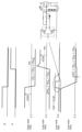
(1)特許文献1の技術について
図1は、特許文献1に開示された従来のスイッチング回路の回路図である。このスイッチング回路は、駆動回路52と、主スイッチング素子51とで構成される。駆動回路52は、コンデンサ60、インバータ70、PMOSのトランジスタ53及びNMOSのトランジスタ54で構成される駆動信号発生回路と、駆動信号発生回路と主スイッチング素子51との間に接続された抵抗器55、56、58、59及びコンデンサ57とを備える。(1) Regarding the technology of
このような構成により、主スイッチング素子51のターンオン時及びターンオフ時のゲート電流経路を分離することで、充電電流及び放電電流を個別かつ最適に調整できるとともに、ターンオン時及びターンオフ時の誤動作を防ぐことが可能となる。よって、主スイッチング素子51に対し、スイッチング速度を調整し、かつ、スイッチング回路における寄生インダクタンスを低減、又は、寄生インダクタンスの影響を抑制することにより、安定に制御されたスイッチング回路が実現される。
With this configuration, by separating the gate current paths during turn-on and turn-off of the
しかしながら、特許文献1の技術では、コンデンサ57の容量値又は電源電圧VDDが大きい場合には、ターンオフ時に主スイッチング素子51のゲート・ソース間に過剰の負バイアスが与えられ、主スイッチング素子51に対するゲート耐圧不良が発生したり、還流動作時のロスが大きくなったりするという第1の問題がある。
However, in the technique of
また、特許文献1の技術では、ターンオン時に主スイッチング素子51のゲート端子に充電された電荷を短時間で放電するためには、抵抗器55及び56の抵抗値を小さくする必要があるが、これらの抵抗値を過剰に小さくすると主スイッチング素子51のゲート電圧が耐圧を超えたり、駆動ロスが大きくなったりするなどの課題が生じるために、抵抗器55及び56の抵抗値を小さくするには限度がある。そのために、主スイッチング素子51に期待される高周波動作に限界があるという第2の問題が生じる。
In addition, in the technique of
(2)特許文献2の技術について
図2は、特許文献2に開示された従来のスイッチング回路の回路図である。このスイッチング回路は、駆動信号発生回路80、スイッチング素子Q11、並びに、駆動信号発生回路80とスイッチング素子Q11との間に接続されたコンデンサC12及び逆バイアス電圧生成回路84で構成される。(2) Regarding the technology of Patent Document 2 FIG. 2 is a circuit diagram of a conventional switching circuit disclosed in Patent Document 2. This switching circuit includes a drive
このような構成により、コンデンサC12の容量とスイッチング素子Q11の入力容量(つまり、寄生容量)とによる電圧分割が行われるので、スイッチング素子Q11の見かけ上の入力容量が小さくなる。その結果、ターンオン時のスイッチング素子Q11のゲート端子の電圧が低電圧化され、スイッチング素子Q11のターンオン動作が高速かつ効率化される。加えて、スイッチング素子Q11のゲート端子とソース端子との間に、ダイオードD11とツェナーダイオードZD11との直列回路からなる逆バイアス電圧生成回路84が接続されている。これにより、ターンオフ時において、スイッチング素子Q11のゲートに対して従来よりも強い逆バイアス電圧が印加されるので、スイッチング素子Q11のターンオフ動作が高速化される。
With this configuration, voltage division is performed by the capacitance of the capacitor C12 and the input capacitance (that is, parasitic capacitance) of the switching element Q11, so that the apparent input capacitance of the switching element Q11 becomes small. As a result, the voltage at the gate terminal of switching element Q11 during turn-on is reduced, and the turn-on operation of switching element Q11 is made faster and more efficient. In addition, a reverse bias
しかしながら、特許文献2の技術では、スイッチング素子Q11のゲート電極がオーミック接合のタイプである場合、ターンオン時に、ゲート・ソース間電圧が2.5~3Vであったとしてもゲート・ソース間に数mA~数10mA程度の電流が流れるため、ゲート・ソース間電圧が減少し、導通状態を維持できないという第3の問題がある。 However, in the technology of Patent Document 2, if the gate electrode of the switching element Q11 is an ohmic junction type, even if the gate-source voltage is 2.5 to 3V at turn-on, the voltage between the gate and source is several mA. The third problem is that since a current of about 10 mA to several tens of mA flows, the voltage between the gate and the source decreases, making it impossible to maintain a conductive state.
また、特許文献2の技術では、ターンオフ時に、誘導性負荷等に起因してソース電位を基準としてドレイン電圧が上昇した場合には、ゲート・ドレイン間の寄生容量への充電電流がコンデンサC12にも電流が流れるため、コンデンサC12が再放電され、ゲート・ソース間電位が増加し、その増加したゲート・ソース間電位がスイッチング素子Q11の閾値を越えた場合には、誤点弧を起こす可能性があるという第4の問題がある。 In addition, in the technology of Patent Document 2, when the drain voltage increases with respect to the source potential due to an inductive load etc. at turn-off, the charging current to the parasitic capacitance between the gate and drain also flows to the capacitor C12. As the current flows, the capacitor C12 is discharged again, and the gate-source potential increases. If the increased gate-source potential exceeds the threshold of the switching element Q11, there is a possibility of false firing. There is a fourth problem.
(3)解決策
そこで、上記特許文献1の技術における第1及び第2の問題、並びに、上記特許文献2の技術における第3及び第4の問題を解決するために、本発明に係るスイッチング回路は、ソース端子、ドレイン端子及びゲート端子を有するノーマリオフ型の接合型電界効果トランジスタと、第1の電源入力端子、前記第1の電源入力端子の電位又はハイインピーダンス状態を出力する第1の出力端子、第2の電源入力端子、前記第2の電源入力端子の電位又はハイインピーダンス状態を出力する第2の出力端子、及び、前記第1の出力端子が前記第1の電源入力端子の電位を出力し、かつ、前記第2の出力端子がハイインピーダンス状態を出力する第1の出力状態と、前記第1の出力端子がハイインピーダンス状態を出力し、かつ、前記第2の出力端子が前記第2の電源入力端子の電位を出力する第2の出力状態とを切り替えるための入力端子を有する駆動部と、前記ソース端子と前記ゲート端子との間に接続され、前記ソース端子側に陽極を有し、前記ゲート端子側に陰極を有する第1の整流素子と、前記第1の出力端子と前記ゲート端子との間に接続された第1の抵抗器と、前記第1の抵抗器と並列に接続された直列回路であって、直列に接続されたコンデンサと第2の抵抗器とを有する直列回路と、前記ゲート端子側に陽極を有し、前記第2の出力端子側に陰極を有する第2の整流素子とを備え、前記ソース端子は、前記第2の電源入力端子と接続され、前記第2の整流素子は、直列に接続された前記コンデンサ及び前記第2の抵抗器のうちの少なくとも前記コンデンサと並列に接続されている。(3) Solution Therefore, in order to solve the first and second problems in the technique of
(実施の形態)
以下、本発明の実施の形態について、図面を用いて詳細に説明する。なお、以下で説明する実施の形態は、いずれも本発明の一具体例を示すものである。以下の実施の形態で示される数値、形状、材料、構成要素、構成要素の配置位置及び接続形態、波形、タイミング等は、一例であり、本発明を限定する主旨ではない。また、以下の実施の形態における構成要素のうち、本発明の最上位概念を示す独立請求項に記載されていない構成要素については、任意の構成要素として説明される。また、各図は、必ずしも厳密に図示したものではない。各図において、実質的に同一の構成については同一の符号を付し、重複する説明は省略又は簡略化する場合がある。(Embodiment)
Hereinafter, embodiments of the present invention will be described in detail using the drawings. Note that all of the embodiments described below are specific examples of the present invention. The numerical values, shapes, materials, components, arrangement positions and connection forms of the components, waveforms, timing, etc. shown in the following embodiments are merely examples, and do not limit the present invention. Further, among the constituent elements in the following embodiments, constituent elements that are not described in the independent claims representing the most significant concept of the present invention will be described as arbitrary constituent elements. Further, each figure is not necessarily strictly illustrated. In each figure, substantially the same configurations are denoted by the same reference numerals, and overlapping explanations may be omitted or simplified.
図3は、実施の形態に係るハーフブリッジ回路10の回路図である。ハーフブリッジ回路10は、ハイサイドとして、スイッチング回路20、インバータ11、電源12、及び、入力端子Bを備え、ローサイドとして、スイッチング回路30、インバータ13、電源14、及び、入力端子Aを備える。また、ハーフブリッジ回路10は、誘導性負荷としてのインダクタ15、及び、負荷用の電源16も備える。
FIG. 3 is a circuit diagram of the
ハイサイド及びローサイドは、同一の回路で構成される。ここでは、ハイサイドに着目して詳細な構成を説明する。 The high side and low side are configured with the same circuit. Here, the detailed configuration will be explained focusing on the high side.
電源12は、スイッチング回路20に直流電圧VDDを供給する。
インバータ11は、入力端子Bに入力された信号を論理反転してスイッチング回路20に出力するバッファである。
The
スイッチング回路20は、スイッチング素子28、駆動部20a、抵抗器23及び24、コンデンサ25、ダイオード26及び27を備える。
The switching
スイッチング素子28は、ソース端子S21、ドレイン端子D21及びゲート端子G21を有するノーマリオフ型の接合型電界効果トランジスタであり、例えば、ワイドバンドギャップ型の化合物半導体であるGaN(窒化ガリウム)を用いてノーマリオフ動作と大電流及び低オン抵抗とを両立したトランジスタである。具体的には、スイッチング素子28は、例えば、p型窒化物半導体、及び、そのp型窒化物半導体とオーミック接触(つまり、オーミック接合)するゲート電極で構成されるゲート部を有するGaN-GIT(Gallium Nitride Gate Injection Transistor)等のGaNトランジスタである。
The switching
GaNトランジスタにおいては、ゲート部にp型窒化物半導体を用いることで、ノーマリオフ型を実現しやすくなる。さらに、ゲート電極がp型窒化物半導体とオーミック接触することで、過剰な正電圧がゲートに印加されてもゲート電流として流すことができるために信頼性が高くなる。一方、ゲート電極がp型窒化物半導体とショットキー接合しているとゲート電流が流れにくい。しかしながら、過剰な正電圧がゲートに印加された場合に、ショットキー接合としては逆バイアスとなるために、ショットキー接合がブレークダウンを起こしてゲート部が破壊しやすくなる。 In a GaN transistor, by using a p-type nitride semiconductor in the gate portion, it becomes easier to realize a normally-off type. Furthermore, since the gate electrode is in ohmic contact with the p-type nitride semiconductor, even if an excessive positive voltage is applied to the gate, the gate current can flow, thereby increasing reliability. On the other hand, if the gate electrode is in a Schottky junction with the p-type nitride semiconductor, gate current will hardly flow. However, when an excessive positive voltage is applied to the gate, the Schottky junction becomes reverse biased, so that the Schottky junction breaks down and the gate portion is likely to be destroyed.
駆動部20aは、ゲート端子G22及びG23同士が接続されたスイッチ素子21及び22で構成された駆動信号発生回路であり、第1の電源入力端子V21、第1の電源入力端子V21の電位VDD又はハイインピーダンス状態を出力する第1の出力端子OUT21、第2の電源入力端子V22、第2の電源入力端子V22の電位GND又はハイインピーダンス状態を出力する第2の出力端子OUT22、及び、第1の出力端子OUT21が第1の電源入力端子V21の電位VDDを出力し、かつ、第2の出力端子OUT22がハイインピーダンス状態を出力する第1の出力状態と、第1の出力端子OUT21がハイインピーダンス状態を出力し、かつ、第2の出力端子OUT22が第2の電源入力端子V22の電位GNDを出力する第2の出力状態とを切り替えるための入力端子IN21を有する。本実施の形態では、スイッチ素子21は、PMOSトランジスタであり、ソース端子S22が第1の電源入力端子V21に接続され、ドレイン端子D22が第1の出力端子OUT21に接続されている。また、スイッチ素子22は、NMOSトランジスタであり、ソース端子S23が第2の電源入力端子V22に接続され、ドレイン端子D23が第2の出力端子OUT22に接続されている。
The
ダイオード27は、スイッチング素子28のソース端子S21とゲート端子G21との間に接続され、ソース端子S21側に陽極(アノード)を有し、ゲート端子G21側に陰極(カソード)を有する第1の整流素子の一例である。
The
抵抗器23は、第1の出力端子OUT21とスイッチング素子28のゲート端子G21との間に接続された第1の抵抗器の一例である。
The
抵抗器24は、コンデンサ25と直列に接続された第2の抵抗器の一例である。抵抗器24とコンデンサ25とからなる直列回路は、抵抗器23と並列に接続されている。
ダイオード26は、スイッチング素子28のゲート端子G21側に陽極を有し、第2の出力端子OUT22側に陰極を有する第2の整流素子の一例である。
The
なお、スイッチング素子28のソース端子S21は、第2の電源入力端子V22と接続されている。
Note that the source terminal S21 of the switching
また、ダイオード26は、直列に接続されたコンデンサ25及び抵抗器24のうちの少なくともコンデンサ25と並列に接続されている。本実施の形態では、ダイオード26は、直列に接続されたコンデンサ25及び抵抗器24のうちのコンデンサ25だけと並列に接続されている。つまり、ダイオード26の陰極は、コンデンサ25と抵抗器24との接続点に接続されている。
Moreover, the
ローサイドのスイッチング回路30についても、ハイサイドのスイッチング回路20と同一の構成を備える。つまり、スイッチング回路30は、スイッチング素子38、駆動部30a、抵抗器33及び34、コンデンサ35、ダイオード36及び37を備える。駆動部30aは、ゲート端子G32、ソース端子S32及びドレイン端子D32を有するスイッチ素子31並びにゲート端子G33、ソース端子S33及びドレイン端子D33を有するスイッチ素子32で構成され、第1の電源入力端子V31、第1の出力端子OUT31、第2の電源入力端子V32、第2の出力端子OUT32、及び、入力端子IN31を有する。
The low-
次に、以上のように構成された実施の形態に係るハーフブリッジ回路10の動作について説明する。
Next, the operation of the
図4は、実施の形態に係るハーフブリッジ回路10におけるスイッチング素子28及び38の駆動に関連する信号の波形を示す図である。ハイサイド及びローサイドのいずれについても同じ波形であるので、ここでは、ハイサイドでの波形を示している。「ゲート・ソース間電圧」は、スイッチング素子28のゲート・ソース間電圧、「ゲート端子電流」は、スイッチング素子28のゲート端子G21に流れ込む電流、「コンデンサ25両端電圧」は、コンデンサ25の両端電圧の波形を示す。
FIG. 4 is a diagram showing waveforms of signals related to driving the
「ゲート・ソース間電圧」の波形に示されるように、入力端子Bの入力信号のHigh及びLowに応じて(図示せず)、駆動部20aが第1の出力状態及び第2の出力状態を交互にとるので、ゲート・ソース間電圧は、スイッチング素子28をターンオンさせるHighと、スイッチング素子28をターンオフさせるLowとを交互に繰り返す。ここで、第1の電源入力端子V21の電源電圧VDDが抵抗器23を介してスイッチング素子28のゲート端子G21に印加されるので、ゲート・ソース間電圧のHighは、スイッチング素子28のゲートが有するダイオード特性で定まる電位VGSF(ゲートクランプ電圧)となる。このように、駆動部20aとスイッチング素子28のゲート端子G21との間に接続された抵抗器23により、スイッチング素子28のターンオン状態が確実に維持され、特許文献2についての第3の問題が解消される。
As shown in the waveform of the "gate-source voltage", the
なお、ゲート・ソース間電圧のLowは、ダイオード27の順方向電圧VfD1で定まる負の電位VfD1となる。また、「ゲート・ソース間電圧」の波形において、立ち上がりは、コンデンサ25のスピードアップ作用により、オーバーシュートしている。コンデンサ25と直列に接続された抵抗器24は、スピードアップ作用の調整だけでなく、ゲート・ソース間電圧の振動を抑制する作用も有しており、これにより、スイッチング素子28の誤動作を抑制している。Note that the low gate-source voltage is a negative potential Vf D1 determined by the forward voltage Vf D1 of the
また、「ゲート端子電流」の波形に示されるように、ゲート端子電流は、スイッチング素子28のゲート容量により、ゲート・ソース間電圧の立ち上がり時及び立下り時において、一時的に大きな電流が流れる。スイッチング素子28がターンオンの定常状態であるときは、ゲート端子電流は、(VDD-VGSF)/R1の電流値となる。R1は、抵抗器23の抵抗値である。このように、抵抗器23は、ターンオンの定常時において駆動部20aからスイッチング素子28に流れる電流を調整している。
Further, as shown in the waveform of "gate terminal current", a large current temporarily flows as the gate terminal current due to the gate capacitance of the switching
「コンデンサ25間電圧」の波形に示されるように、コンデンサ25の両端電圧は、入力端子Bの入力信号のHigh及びLowに応じて(図示せず)、充電時の電圧と放電時の電圧とを交互に繰り返す。ここで、充電時の電圧は、(VDD-VGSF)であり、放電時の電圧は、VfD1となる。As shown in the waveform of "voltage across
図5は、実施の形態に係るハーフブリッジ回路10の第1の動作を示すタイミングチャートである。ここで、第1の動作とは、ハイサイドのスイッチング素子28がターンオン状態からターンオフ状態に変化し、逆に、ローサイドのスイッチング素子38がターンオフ状態からターンオン状態に変化する動作である。また、「B」は、ハイサイドの入力端子Bに入力される信号、「A」は、ローサイドの入力端子Aに入力される信号、「High-side VGS」は、ハイサイドのスイッチング素子28のゲート・ソース間電圧、「Low-side VGS」は、ローサイドのスイッチング素子38のゲート・ソース間電圧、「Low-side IGD」は、ローサイドのスイッチング素子38のゲート・ドレイン電流、「Low-side VDS」は、ローサイドのスイッチング素子38のドレイン・ソース間電圧、の波形を示す。
FIG. 5 is a timing chart showing the first operation of the
「B」、「A」の波形に示されるように、本図では、ハイサイドの入力端子Bの入力信号がHighからLowに変化し、ローサイドの入力端子Aの入力信号がLowからHighに変化するときのタイミングが示されている。 As shown in the waveforms "B" and "A", in this diagram, the input signal at the high-side input terminal B changes from High to Low, and the input signal at the low-side input terminal A changes from Low to High. The timing is shown.
「High-side VGS」の波形に示されるように、ハイサイドでは、入力端子Bの入力信号がHighからLowに変化することで、スイッチ素子21がオンで、かつ、スイッチ素子22がオフの第1の出力状態から、スイッチ素子21がオフで、かつ、スイッチ素子22がオンの第2の出力状態に変化し、その結果、スイッチング素子28のゲート・ソース間電圧VGSは、ターンオンさせるHigh(つまり、電位VGSF)からターンオフさせるLow(つまり、負の電位VfD1)に変化する。As shown in the "High-side VGS" waveform, on the high side, the input signal at input terminal B changes from High to Low, causing the
また、「Low-side VGS」の波形に示されるように、ローサイドでは、入力端子Aの入力信号がLowからHighに変化することで、スイッチ素子31がオフで、かつ、スイッチ素子32がオンの第2の出力状態から、スイッチ素子31がオンで、かつ、スイッチ素子32がオフの第1の出力状態に変化し、その結果、スイッチング素子38のゲート・ソース間電圧VGSは、ターンオフさせるLow(つまり、負の電位VfD1)からターンオンさせるHigh(つまり、電位VGSF)に変化する。なお、電圧VfD1は、ダイオード37の順方向電圧である。また、電位VGSFは、スイッチング素子38のゲートが有するダイオード特性で定まるゲートクランプ電圧である。また、図中の「Vth」は、スイッチング素子38の閾値電圧である。Furthermore, as shown in the "Low-side VGS" waveform, on the low side, the input signal at the input terminal A changes from Low to High, causing the
また、「Low-side IGD」の波形に示されるように、ハイサイドのスイッチング素子28がターンオン状態からターンオフ状態となったときに、ローサイドでは、スイッチング素子38はターンオフ状態ではあるが、誘導性負荷であるインダクタ15に起因して、インダクタ15に向かって流れる電流をスイッチング素子38のソースからドレインに向かって通電しようとする。そのためドレイン・ソース間電圧VDSは急速に下降し、ゲート・ドレイン間容量CGDに充電された電荷は急速に放電される。これにより、ゲート端子G31からゲート・ドレイン間容量CGDを介してドレイン端子D31に至る経路で、ゲート・ドレイン電流IGDが流れる。このゲート・ドレイン電流IGDの大きさは、ゲート・ドレイン間容量CGDと、ゲート・ドレイン間容量CGDの両端電圧vの変化率とに依存して定まる値(つまり、CGD×dv/dt)である。ここで、スイッチング素子38のゲート端子G31の電位は、ダイオード36によってクランプされるので、ゲート電位に影響がない(つまり、スイッチング素子38がターンオンすることが抑制される)。
Further, as shown in the waveform of "Low-side IGD", when the high-
また、「Low-side VDS」の波形に示されるように、ローサイドでは、スイッチング素子38の還流動作において、スイッチング素子38のドレイン・ソース間電圧VDSが下降していくが、ダイオード37により、ゲート・ソース間電圧VGSは、減少することなく一定値(つまり、-VfD1)となる。スイッチング素子38がソースからドレインに向かって還流電流を通電し、還流動作を行うためにはドレイン電圧がゲート電圧よりもソース・ドレイン電圧VSD分低い電圧となる必要がある。よって、ドレイン・ソース間電圧VDSは、下降した後、負の電位(具体的には、負の電位(ソース・ドレイン電圧VSD+VfD1))となる。これにより、ゲート端子G31への負バイアスが増大することによるスイッチング素子38のゲートの耐圧破壊や還流動作による損失の悪化が抑制される。これにより、特許文献1についての第1の問題が解消される。Further, as shown in the waveform "Low-side VDS", on the low side, the drain-source voltage VDS of the switching
図6は、実施の形態に係るハーフブリッジ回路10の第2の動作を示すタイミングチャートである。ここで、第2の動作とは、ハイサイドのスイッチング素子28がターンオフ状態からターンオン状態に変化し、逆に、ローサイドのスイッチング素子38がターンオン状態からターンオフ状態に変化する動作である。図示されている信号は、図4と同じである。
FIG. 6 is a timing chart showing the second operation of the
「B」、「A」の波形に示されるように、本図では、ハイサイドの入力端子Bの入力信号がLowからHighに変化し、ローサイドの入力端子Aの入力信号がHighからLowに変化するときのタイミングが示されている。 As shown in the waveforms "B" and "A", in this figure, the input signal at the high-side input terminal B changes from Low to High, and the input signal at the low-side input terminal A changes from High to Low. The timing is shown.
「High-side VGS」の波形に示されるように、ハイサイドでは、入力端子Bの入力信号がLowからHighに変化することで、スイッチ素子21がオフで、かつ、スイッチ素子22がオンの第2の出力状態から、スイッチ素子21がオンで、かつ、スイッチ素子22がオフの第1の出力状態に変化し、その結果、スイッチング素子28のゲート・ソース間電圧VGSは、ターンオフさせるLow(つまり、負の電位VfD1)からターンオンさせるHigh(つまり、電位VGSF)に変化する。なお、図中の「Vth」は、スイッチング素子28の閾値電圧である。As shown in the "High-side VGS" waveform, on the high side, the input signal at input terminal B changes from Low to High, causing the
また、「Low-side VGS」の波形に示されるように、ローサイドでは、入力端子Aの入力信号がHighからLowに変化することで、スイッチ素子31がオンで、かつ、スイッチ素子32がオフの第1の出力状態から、スイッチ素子31がオフで、かつ、スイッチ素子32がオンの第2の出力状態に変化し、その結果、スイッチング素子38のゲート・ソース間電圧VGSは、ターンオンさせるHighからターンオフさせるLow(つまり、負の電位VfD1)に変化する。その後、ハイサイドのスイッチング素子28がターンオンしたときに(つまり、「High-side VGS」でゲート・ソース間電圧VGSがHighになったときに)、ローサイドでは、スイッチング素子38のドレイン端子D31にスイッチング素子28のソース端子S21から出力された電圧が印加されるので、スイッチング素子38のゲート・ドレイン間容量CGDを介してドレイン端子D31からゲート端子G31に電圧が印加され、ゲート・ソース間電圧VGSは、「Low-side IGD」の波形の説明で述べる理由により、ダイオード36の順方向電圧に相当する電位VfD2まで上昇する。なお、電位VfD2は、スイッチング素子38の閾値電圧Vthよりも低い。また、図中の期間(i)及び(ii)は、それぞれ、ゲート・ソース間電圧VGSの上昇における立ち上がり期間及び立ち上がった後の期間である。Furthermore, as shown in the "Low-side VGS" waveform, on the low side, the input signal at the input terminal A changes from High to Low, causing the
また、「Low-side IGD」の波形に示されるように、ハイサイドのスイッチング素子28がターンオンしたときに(「High-side VGS」でゲート・ソース間電圧VGSがHighになったときに)、ローサイドでは、上述したように、スイッチング素子38のドレイン端子D31にスイッチング素子28のソース端子S21から出力された電圧が印加されるので、スイッチング素子38のドレイン端子D31から、ゲート・ドレイン間容量CGD、ゲート端子G31、コンデンサ35及びダイオード36の並列回路、及び、スイッチ素子32を介してGNDに向けて、ゲート・ドレイン電流IGD(つまり、負のゲート・ドレイン電流IGD)が流れる。
Furthermore, as shown in the waveform of "Low-side IGD", when the high-
より詳しくは、上記期間(i)では、スイッチング素子38のドレイン端子D31から、ゲート・ドレイン間容量CGD、ゲート端子G31、コンデンサ35、及び、スイッチ素子32を介してGNDに向けて、ゲート・ドレイン電流IGDが流れ、コンデンサ35の電圧が徐々に増大して電圧VfD2に達する。その後は(つまり、期間(ii)では)、ダイオード36によるクランプにより、スイッチング素子38のドレイン端子D31から、ゲート・ドレイン間容量CGD、ゲート端子G31、ダイオード36、及び、スイッチ素子32を介してGNDに向けて、ゲート・ドレイン電流IGDが流れる。これにより、「Low-side VGS」の波形に示されるように、ゲート・ソース間電圧VGSは、ダイオード36の順方向電圧に相当する電位VfD2まで上昇するが、スイッチング素子38の閾値電圧Vthを超えないので、スイッチング素子28及び38が同時にオンする誤点弧が抑制され、特許文献2についての第4の問題が解消される。また、ダイオード36により、抵抗器33及び34の抵抗値を小さくすることなく、スイッチング素子38のゲート端子G31に充電された電荷を短時間で放電することができるので、スイッチング素子38の高周波動作の限界が緩和され、特許文献1についての第2の問題も解消される。More specifically, in the period (i), the gate-drain is connected from the drain terminal D31 of the switching
また、「Low-side VDS」の波形に示されるように、ハイサイドのスイッチング素子28がターンオンしたときに(つまり、「High-side VGS」でゲート・ソース間電圧VGSがHighになったときに)、ローサイドでは、上述したように、スイッチング素子38のドレイン端子D31にスイッチング素子28のソース端子S21から出力された電圧が印加されるので、スイッチング素子38のドレイン・ソース間電圧VDSは上昇する。
In addition, as shown in the waveform of "Low-side VDS", when the high-
以上のように、本実施の形態に係るスイッチング回路30(及び、スイッチング回路20についても同様)は、ソース端子S31、ドレイン端子D31及びゲート端子G31を有する、ノーマリオフ型の接合型電界効果トランジスタであるスイッチング素子38と、第1の電源入力端子V31、第1の電源入力端子V31の電位VDD又はハイインピーダンス状態を出力する第1の出力端子OUT31、第2の電源入力端子V32、第2の電源入力端子V32の電位GND又はハイインピーダンス状態を出力する第2の出力端子OUT32、及び、第1の出力端子OUT31が第1の電源入力端子V31の電位VDDを出力し、かつ、第2の出力端子OUT32がハイインピーダンス状態を出力する第1の出力状態と、第1の出力端子OUT31がハイインピーダンス状態を出力し、かつ、第2の出力端子OUT32が第2の電源入力端子V32の電位GNDを出力する第2の出力状態とを切り替えるための入力端子IN3を有する駆動部30aと、スイッチング素子38のソース端子S31とゲート端子G31との間に接続され、ソース端子S31側に陽極(アノード)を有し、ゲート端子G31側に陰極(カソード)を有する第1の整流素子であるダイオード37と、第1の出力端子OUT31とスイッチング素子38のゲート端子G31との間に接続された第1の抵抗器である抵抗器33と、第1の抵抗器と並列に接続された直列回路であって、直列に接続されたコンデンサ35と抵抗器33とを有する直列回路と、スイッチング素子38のゲート端子G31側に陽極を有し、第2の出力端子OUT32側に陰極を有する第2の整流素子であるダイオード36とを備える。スイッチング素子38のソース端子S31は、第2の電源入力端子V32と接続され、ダイオード36は、直列に接続されたコンデンサ35及び抵抗器34のうちの少なくともコンデンサ35(ここでは、コンデンサ35だけ)と並列に接続されている。
As described above, the switching circuit 30 (and the same applies to the switching circuit 20) according to the present embodiment is a normally-off junction field effect transistor having a source terminal S31, a drain terminal D31, and a gate terminal G31. A switching
これにより、スイッチング素子38のゲート端子G31とソース端子S31との間にはダイオード37が接続されるので、ゲート端子G31への負バイアスが増大することによるスイッチング素子38のゲートの耐圧破壊や還流動作による損失の悪化が抑制され、特許文献1についての第1の問題が解消される。
As a result, the
また、コンデンサ35と並列にダイオード36が接続され、コンデンサ35とゲート端子G31との接続部とソース端子S31との間にダイオード37が接続されているので、抵抗器33及び34の抵抗値を小さくすることなく、駆動部30aが第1の出力状態から第2の出力状態に変化した際に、コンデンサ35に充電された一部の電荷によってゲート端子G31の電荷が放電されつつ、さらに残っているコンデンサ35に充電された電荷が短時間で放電され、スイッチング素子38の高周波動作の限界が緩和され、特許文献1についての第2の問題が解消される。
In addition, a
また、駆動部30aとスイッチング素子38のゲート端子G31との間に抵抗器33が接続されているので、スイッチング素子38のターンオン状態が確実に維持され、特許文献2についての第3の問題が解消される。
Furthermore, since the
また、コンデンサ35と並列にダイオード36が接続されているので、スイッチング素子28がターンオンしたときに、ターンオフ状態にあるスイッチング素子38のゲート・ソース間電圧VGSは、ダイオード36の順方向電圧に相当する電位VfD2までしか上昇しない。よって、スイッチング素子28及び38が同時にオンする誤点弧が抑制され、特許文献2についての第4の問題が解消される。Further, since the
よって、スイッチング素子38を駆動するスイッチング回路であって、スイッチング素子38に対するゲート耐圧不良の発生を抑制し、還流動作時のロスを抑制し、スイッチング素子38の高周波動作の限界を緩和し、ターンオン時の導通状態をより確実に維持し、かつ、誤点弧の発生を抑制することができるスイッチング回路30が実現される。
Therefore, the switching circuit that drives the switching
特に、スイッチング素子28及び38が、ゲート部がp型窒化物半導体、及び、p型窒化物半導体にオーミック接触するゲート電極で構成されるGaNトランジスタの場合において、ターンオン時に数mA~数10mAの電流を流し続けることができる。したがって、誤点弧を起こしにくく、かつ信頼性の高いスイッチング回路を実現できる。
In particular, in the case where the switching
(変形例1)
次に、上記実施の形態の変形例1に係るスイッチング回路40について説明する。(Modification 1)
Next, a switching
図7は、実施の形態の変形例1に係るスイッチング回路40の回路図である。このスイッチング回路40は、上記実施の形態に係るスイッチング回路20及び30に置き換えられ得るスイッチング回路である。
FIG. 7 is a circuit diagram of a switching
スイッチング回路40は、ダイオード36の接続形態を除いて、上記実施の形態に係るスイッチング回路20及び30と同じ構成を備える。つまり、本変形例では、スイッチング回路40は、上記実施の形態に係るスイッチング回路30において、ダイオード36が、直列に接続されたコンデンサ35及び抵抗器34と並列に接続されている。具体的には、ダイオード36の陽極は、スイッチング素子38のゲート端子G31に接続され、陰極は、駆動部30aの第1の出力端子OUT31と第2の出力端子OUT32との接続点に接続されている。
The switching
図8は、実施の形態の変形例1に係るスイッチング回路40をローサイドのスイッチング回路として適用したハーフブリッジ回路の第2の動作を示すタイミングチャートである。
FIG. 8 is a timing chart showing a second operation of a half-bridge circuit in which the
「Low-side IGD」の波形に示されるように、ハイサイドのスイッチング素子28がターンオンしたときに(「High-side VGS」でゲート・ソース間電圧VGSがHighになったときに)、ローサイドでは、スイッチング素子38のドレイン端子D31にスイッチング素子28のソース端子S21から出力された電圧が印加されるが、期間(i)では、スイッチング素子38のドレイン端子D31から、ゲート・ドレイン間容量CGD、ゲート端子G31、コンデンサ35、抵抗器34、及び、スイッチ素子32を介してGNDに向けて、ゲート・ドレイン電流IGDが流れ、コンデンサ35の電圧が徐々に増大して電圧VfD2に達する。その後は(つまり、期間(ii)では)、上記実施の形態と同様に、ダイオード36によるクランプにより、スイッチング素子38のドレイン端子D31から、ゲート・ドレイン間容量CGD、ゲート端子G31、ダイオード36、及び、スイッチ素子32を介してGNDに向けて、ゲート・ドレイン電流IGDが流れる。As shown in the waveform of "Low-side IGD", when the high-
これにより、上記実施の形態と同様に、ゲート・ソース間電圧VGSは、ダイオード36の順方向電圧に相当する電位VfD2まで上昇するが、スイッチング素子38の閾値電圧Vthを超えないので、スイッチング素子28及び38が同時にオンする誤点弧が抑制される。As a result, as in the above embodiment, the gate-source voltage VGS rises to the potential VfD2 corresponding to the forward voltage of the
また、駆動部30aの第1の出力端子OUT31及び第2の出力端子OUT32が短絡されているので、第1の出力端子OUT31及び第2の出力端子OUT32が共通の端子となった駆動部30aを用いてスイッチング回路40を構築できる。つまり、スイッチング回路30を構成する駆動部30aとして、1出力タイプの駆動デバイスを使うことで、より汎用的な駆動デバイスを利用することができ、スイッチング回路30のコストを削減できる。
Furthermore, since the first output terminal OUT31 and the second output terminal OUT32 of the
(変形例2)
次に、上記実施の形態の変形例2に係るスイッチング回路41について説明する。(Modification 2)
Next, a switching
図9は、実施の形態の変形例2に係るスイッチング回路41の回路図である。このスイッチング回路41は、上記実施の形態に係るスイッチング回路20及び30に置き換えられ得るスイッチング回路である。
FIG. 9 is a circuit diagram of a switching
スイッチング回路41は、ダイオード39が追加されている点を除いて、上記実施の形態の変形例1に係るスイッチング回路40と同じ構成を備える。つまり、本変形例では、スイッチング回路41は、上記実施の形態の変形例1に係るスイッチング回路40の構成に加えて、抵抗器34と並列に接続され、コンデンサ35側に陽極を有し、抵抗器33側に陰極を有する第3の整流素子の一例であるダイオード39を備える。
The switching
図10は、実施の形態の変形例2に係るスイッチング回路41をローサイドのスイッチング回路として適用したハーフブリッジ回路の第2の動作を示すタイミングチャートである。
FIG. 10 is a timing chart showing a second operation of a half-bridge circuit in which the
「Low-side IGD」の波形に示されるように、ハイサイドのスイッチング素子28がターンオンしたときに(「High-side VGS」でゲート・ソース間電圧VGSがHighになったときに)、ローサイドでは、スイッチング素子38のドレイン端子D31にスイッチング素子28のソース端子S21から出力された電圧が印加されるが、期間(i)では、スイッチング素子38のドレイン端子D31から、ゲート・ドレイン間容量CGD、ゲート端子G31、コンデンサ35、ダイオード39、及び、スイッチ素子32を介してGNDに向けて、ゲート・ドレイン電流IGDが流れ、コンデンサ35の電圧が徐々に増大して電圧VfD2に達する。その後は(つまり、期間(ii)では)、上記実施の形態と同様に、ダイオード36によるクランプにより、スイッチング素子38のドレイン端子D31から、ゲート・ドレイン間容量CGD、ゲート端子G31、ダイオード36、及び、スイッチ素子32を介してGNDに向けて、ゲート・ドレイン電流IGDが流れる。As shown in the waveform of "Low-side IGD", when the high-
つまり、期間(i)では、ゲート・ドレイン電流IGDは、抵抗器34に代えて、ダイオード39を流れるように、バイパスされる。
That is, in period (i), the gate-drain current IGD is bypassed so that it flows through the
これにより、上記変形例1では、スイッチング素子28のターンオフの瞬間に過大なゲート・ドレイン電流IGDが抵抗器34に流れて発生する電圧によって誤点弧を起こすリスクがあったが、本変形例では、バイパス用のダイオード39により、そのリスクが低減される。
As a result, in the
(変形例3)
次に、上記実施の形態の変形例3に係るスイッチング回路42について説明する。(Modification 3)
Next, a switching
図11は、実施の形態の変形例3に係るスイッチング回路42の回路図である。このスイッチング回路42は、上記実施の形態に係るスイッチング回路20及び30に置き換えられ得るスイッチング回路である。
FIG. 11 is a circuit diagram of a switching
スイッチング回路42は、ツェナーダイオード37aが追加されている点を除いて、上記実施の形態に係るスイッチング回路20及び30と同じ構成を備える。つまり、本変形例では、スイッチング回路42は、上記実施の形態に係るスイッチング回路20又は30(ここでは、スイッチング回路30)の構成に加えて、ソース端子S31とゲート端子G31との間で、かつ、ダイオード37と直列に接続され、ゲート端子G31側に陽極を有し、ソース端子S31側に陰極を有するツェナーダイオード37aを備える。
The switching
図12は、実施の形態の変形例3に係るスイッチング回路42をハイサイド及びローサイドのスイッチング回路として適用したハーフブリッジ回路の第1の動作を示すタイミングチャートである。
FIG. 12 is a timing chart showing a first operation of a half-bridge circuit in which the
「Low-side VGS」の波形に示されるように、ローサイドでは、入力端子Aの入力信号がLowからHighに変化することで、スイッチング素子38のゲート・ソース間電圧VGSは、ターンオフさせるLow(つまり、負の電位(VbZD1+VfD1))からターンオンさせるHigh(つまり、電位VGSF)に変化する。なお、電圧VbZD1は、ツェナーダイオード37aのツェナー電圧である。電圧VfD1は、ダイオード37の順方向電圧である。As shown in the "Low-side VGS" waveform, on the low side, as the input signal at the input terminal A changes from Low to High, the gate-source voltage VGS of the switching
また、「Low-side IGD」の波形に示されるように、ハイサイドのスイッチング素子28がターンオン状態からターンオフ状態となったときに、ローサイドでは、スイッチング素子38はターンオフ状態ではあるが、誘導性負荷であるインダクタ15に起因して、インダクタ15に向かって流れる電流をスイッチング素子38のソースからドレインに向かって通電しようとする。そのためドレイン・ソース間電圧VDSは急速に下降し、ゲート・ドレイン間容量CGDに充電された電荷は急速に放電される。これにより、ゲート端子G31からゲート・ドレイン間容量CGDを介してドレイン端子D31に至る経路で、ゲート・ドレイン電流IGDが流れる。このゲート・ドレイン電流IGDは、ゲート端子G31から第2の出力端子OUT32、及び、第2の電源入力端子V32からソース端子S31にかけての寄生インダクタンスに誘導起電力を発生させ、電圧や発振状態を起こす。これらの電圧はダイオード36によってクランプされることなくゲート・ソース間電圧VGSに重畳され、誤点弧のリスクとなり得る。これに対して、ツェナーダイオード37aを挿入することでゲート・ソース間の負バイアスを大きくし、ターンオフ時の放電量を調整することで、誘導起電力によって電圧が重畳しても誤点弧が起こらない対策をすることが可能になる。また、ツェナー電圧の違うツェナーダイオード37aを選択することで、ゲート端子G31への負バイアスの値を細かく調整できるようになるため、誤点弧リスクと負バイアスの増加による還流時の損失とのトレードオフを調整しやすくなり、高速な動作を行うスイッチング素子38の性能を極限まで引き出すことができる。
Further, as shown in the waveform of "Low-side IGD", when the high-
また、「Low-side VDS」の波形に示されるように、ローサイドでは、スイッチング素子38の還流動作において、スイッチング素子38のドレイン・ソース間電圧VDSが下降していくが、ツェナーダイオード37a及びダイオード37により、ゲート・ソース間電圧VGSは、減少することなく一定値(つまり、-VbZD1-VfD1)となる。スイッチング素子38がソースからドレインに向かって還流電流を通電し、還流動作を行うためにはドレイン電圧がゲート電圧よりもソース・ドレイン電圧VSD分低い電圧となる必要がある。よって、ドレイン・ソース間電圧VDSは、下降した後、負の電位(具体的には、負の電位(ソース・ドレイン電圧VSD+VbZD1+VfD1))となる。Further, as shown in the waveform "Low-side VDS", on the low side, the drain-source voltage VDS of the switching
図13は、実施の形態の変形例3に係るスイッチング回路42をハイサイド及びローサイドのスイッチング回路として適用したハーフブリッジ回路の第2の動作を示すタイミングチャートである。
FIG. 13 is a timing chart showing a second operation of a half-bridge circuit in which the
「Low-side VGS」の波形に示されるように、ローサイドでは、入力端子Aの入力信号がHighからLowに変化することで、スイッチ素子31がオンで、かつ、スイッチ素子32がオフの第1の出力状態から、スイッチ素子31がオフで、かつ、スイッチ素子32がオンの第2の出力状態に変化し、その結果、スイッチング素子38のゲート・ソース間電圧VGSは、ターンオンさせるHighからターンオフさせるLow(つまり、負の電位(VbZD1+VfD1))に変化する。このように、ゲート・ソース間電圧VGSのLowでは、実施の形態よりも、ツェナーダイオード37aのツェナー電圧VbZD1の分だけ負にバイアスされる。As shown in the "Low-side VGS" waveform, on the low side, the input signal at the input terminal A changes from High to Low, so that the
また、「Low-side IGD」の波形に示されるように、ハイサイドのスイッチング素子28がターンオンしたときに(「High-side VGS」でゲート・ソース間電圧VGSがHighになったときに)、ローサイドでは、スイッチング素子38のドレイン端子D31から、ゲート・ドレイン間容量CGD、ゲート端子G31、コンデンサ35及びダイオード36の並列回路、及び、スイッチ素子32を介してGNDに向けて、ゲート・ドレイン電流IGDが流れる。
Furthermore, as shown in the waveform of "Low-side IGD", when the high-
より詳しくは、上記期間(i)では、スイッチング素子38のドレイン端子D31から、ゲート・ドレイン間容量CGD、ゲート端子G31、コンデンサ35、及び、スイッチ素子32を介してGNDに向けて、ゲート・ドレイン電流IGDが流れ、コンデンサ35の電圧が徐々に増大して電圧VfD2に達する。その後は(つまり、期間(ii)では)、ダイオード36によるクランプにより、スイッチング素子38のドレイン端子D31から、ゲート・ドレイン間容量CGD、ゲート端子G31、ダイオード36、及び、スイッチ素子32を介してGNDに向けて、ゲート・ドレイン電流IGDが流れる。これにより、「Low-side VGS」の波形に示されるように、ゲート・ソース間電圧VGSは、ダイオード36の順方向電圧に相当する電位VfD2まで上昇するが、スイッチング素子38の閾値電圧Vthを超えない。つまり、本変形例では、コンデンサ35に残っている負バイアス量がツェナーダイオード37aによって増加しているため、コンデンサ35の容量値が十分に大きければ、コンデンサ35の電位変化が抑えられ、ダイオード36が導通せずにスイッチング(スイッチング素子38のターンオフ)が完了し、誤点弧のリスクが低減される。よって、スイッチング素子28及び38が同時にオンする誤点弧が抑制され、特許文献2についての第4の問題が解消される。More specifically, in the period (i), the gate-drain is connected from the drain terminal D31 of the switching
また、「Low-side VDS」の波形に示されるように、ハイサイドのスイッチング素子28がターンオンしたときに(つまり、「High-side VGS」でゲート・ソース間電圧VGSがHighになったときに)、ローサイドでは、上述したように、スイッチング素子38のドレイン端子D31にスイッチング素子28のソース端子S21から出力された電圧が印加されるので、スイッチング素子38のドレイン・ソース間電圧VDSは、Low(つまり、負の電位(ソース・ドレイン電圧VSD+VbZD1+VfD1))からHighに向けて上昇する。In addition, as shown in the waveform of "Low-side VDS", when the high-
以上のように、本変形例に係るスイッチング回路42によれば、ダイオード37と直列にツェナーダイオード37aが接続されているので、スイッチング素子38の還流動作時に、ゲート・ソース間電圧VGSの負バイアスを大きくでき、誤点弧リスクが低減される。
As described above, according to the switching
(変形例4)
次に、上記実施の形態の変形例4に係るスイッチング回路43について説明する。(Modification 4)
Next, a switching
図14は、実施の形態の変形例4に係るスイッチング回路43の回路図である。このスイッチング回路43は、上記変形例3に係るスイッチング回路42におけるツェナーダイオード37aを少なくとも1つの整流素子(本変形例では、2つのダイオード37b及び37c)に置き換えた回路に相当する。つまり、本変形例では、スイッチング回路43は、上記実施の形態に係るスイッチング回路20又は30(ここでは、スイッチング回路30)の構成に加えて、)ソース端子S31とゲート端子G31との間で、かつ、ダイオード37と直列に接続され、ゲート端子G31側に陽極を有し、ソース端子S31側に陰極を有する少なくとも1つの整流素子(ここでは、2つのダイオード37b及び37c)を備える。
FIG. 14 is a circuit diagram of a switching
図15は、実施の形態の変形例4に係るスイッチング回路43をハイサイド及びローサイドのスイッチング回路として適用したハーフブリッジ回路の第1の動作を示すタイミングチャートである。
FIG. 15 is a timing chart showing a first operation of a half-bridge circuit in which the
「Low-side VGS」の波形に示されるように、ローサイドでは、入力端子Aの入力信号がLowからHighに変化することで、スイッチング素子38のゲート・ソース間電圧VGSは、ターンオフさせるLow(つまり、負の電位(VfD1+VfD4+VfD5))からターンオンさせるHigh(つまり、電位VGSF)に変化する。なお、電圧VfD4及びVfD5は、それぞれ、ダイオード37b及び37cの順方向電圧である。As shown in the "Low-side VGS" waveform, on the low side, as the input signal at the input terminal A changes from Low to High, the gate-source voltage VGS of the switching
また、「Low-side IGD」の波形に示されるように、ハイサイドのスイッチング素子28がターンオン状態からターンオフ状態となったときに、ローサイドでは、スイッチング素子38はターンオフ状態ではあるが、誘導性負荷であるインダクタ15に起因して、インダクタ15に向かって流れる電流をスイッチング素子38のソースからドレインに向かって通電しようとする。そのためドレイン・ソース間電圧VDSは急速に下降し、ゲート・ドレイン間容量CGDに充電された電荷は急速に放電される。これにより、ゲート端子G31からゲート・ドレイン間容量CGDを介してドレイン端子D31に至る経路で、ゲート・ドレイン電流IGDが流れる。このゲート・ドレイン電流IGDは、ゲート端子G31から第2の出力端子OUT32、及び、第2の電源入力端子V32からソース端子S31にかけての寄生インダクタンスに誘導起電力を発生させ、電圧や発振状態を起こす。これらの電圧はダイオード36によってクランプされることなくゲート・ソース間電圧VGSに重畳され、誤点弧のリスクとなり得る。これに対して、ダイオード37b及び37cを挿入することでゲート・ソース間の負バイアスを大きくし、ターンオフ時の放電量を調整することで、誘導起電力によって電圧が重畳しても誤点弧が起こらない対策をすることが可能になる。また、順方向電圧の異なるダイオード37b及び37cやその個数を選択することで、ゲート端子G31への負バイアスの値を細かく調整できるようになるため、誤点弧リスクと負バイアスの増加による還流時の損失とのトレードオフを調整しやすくなり、高速な動作を行うスイッチング素子38の性能を極限まで引き出すことができる。
Further, as shown in the waveform of "Low-side IGD", when the high-
また、「Low-side VDS」の波形に示されるように、ローサイドでは、スイッチング素子38の還流動作において、スイッチング素子38のドレイン・ソース間電圧VDSが下降していくが、ダイオード37、37b及び37cにより、ゲート・ソース間電圧VGSは、減少することなく一定値(具体的には、負の電位(ソース・ドレイン電圧VSD+VfD1+VfD4+VfD5))となる。Further, as shown in the waveform "Low-side VDS", on the low side, the drain-source voltage VDS of the switching
図16は、実施の形態の変形例4に係るスイッチング回路43をハイサイド及びローサイドのスイッチング回路として適用したハーフブリッジ回路の第2の動作を示すタイミングチャートである。
FIG. 16 is a timing chart showing a second operation of a half-bridge circuit in which the
「Low-side VGS」の波形に示されるように、ローサイドでは、入力端子Aの入力信号がHighからLowに変化することで、スイッチ素子31がオンで、かつ、スイッチ素子32がオフの第1の出力状態から、スイッチ素子31がオフで、かつ、スイッチ素子32がオンの第2の出力状態に変化し、その結果、スイッチング素子38のゲート・ソース間電圧VGSは、ターンオンさせるHighからターンオフさせるLow(つまり、負の電位(VfD1+VfD4+VfD5))に変化する。このように、ゲート・ソース間電圧VGSのLowでは、実施の形態よりも、ダイオード37b及び37cの分だけ負にバイアスされる。As shown in the "Low-side VGS" waveform, on the low side, the input signal at the input terminal A changes from High to Low, so that the
また、「Low-side IGD」の波形に示されるように、ハイサイドのスイッチング素子28がターンオンしたときに(「High-side VGS」でゲート・ソース間電圧VGSがHighになったときに)、ローサイドでは、スイッチング素子38のドレイン端子D31から、ゲート・ドレイン間容量CGD、ゲート端子G31、コンデンサ35及びダイオード36の並列回路、及び、スイッチ素子32を介してGNDに向けて、ゲート・ドレイン電流IGDが流れる。
Furthermore, as shown in the waveform of "Low-side IGD", when the high-
より詳しくは、上記期間(i)では、スイッチング素子38のドレイン端子D31から、ゲート・ドレイン間容量CGD、ゲート端子G31、コンデンサ35、及び、スイッチ素子32を介してGNDに向けて、ゲート・ドレイン電流IGDが流れ、コンデンサ35の電圧が徐々に増大して電圧VfD2に達する。その後は(つまり、期間(ii)では)、ダイオード36によるクランプにより、スイッチング素子38のドレイン端子D31から、ゲート・ドレイン間容量CGD、ゲート端子G31、ダイオード36、及び、スイッチ素子32を介してGNDに向けて、ゲート・ドレイン電流IGDが流れる。これにより、「Low-side VGS」の波形に示されるように、ゲート・ソース間電圧VGSは、ダイオード36の順方向電圧に相当する電位VfD2まで上昇するが、スイッチング素子38の閾値電圧Vthを超えない。つまり、本変形例では、コンデンサ35に残っている負バイアス量がダイオード37b及び37cによって増加しているため、コンデンサ35の容量値が十分に大きければ、コンデンサ35の電位変化が抑えられ、ダイオード36が導通せずにスイッチング(スイッチング素子38のターンオフ)が完了し、誤点弧のリスクが低減される。よって、スイッチング素子28及び38が同時にオンする誤点弧が抑制され、特許文献2についての第4の問題が解消される。More specifically, in the period (i), the gate-drain is connected from the drain terminal D31 of the switching
また、「Low-side VDS」の波形に示されるように、ハイサイドのスイッチング素子28がターンオンしたときに(つまり、「High-side VGS」でゲート・ソース間電圧VGSがHighになったときに)、ローサイドでは、上述したように、スイッチング素子38のドレイン端子D31にスイッチング素子28のソース端子S21から出力された電圧が印加されるので、スイッチング素子38のドレイン・ソース間電圧VDSは、Low(つまり、負の電位(ソース・ドレイン電圧VSD+VfD1+VfD4+VfD5))からHighに向けて上昇する。In addition, as shown in the waveform of "Low-side VDS", when the high-
以上のように、本変形例に係るスイッチング回路43によれば、ダイオード37と直列に少なくとも1つのダイオード37b及び37cが接続されているので、スイッチング素子38の還流動作時に、ゲート・ソース間電圧VGSの負バイアスを大きくでき、誤点弧リスクが低減される。
As described above, according to the switching
(変形例5)
次に、上記実施の形態の変形例5に係るスイッチング回路44について説明する。(Modification 5)
Next, a switching
図17は、実施の形態の変形例5に係るスイッチング回路44の回路図である。このスイッチング回路44は、上記実施の形態に係るスイッチング回路20又は30(ここでは、スイッチング回路30)の構成に加えて、さらに、スイッチング素子38、第1の出力端子OUT31、第2の出力端子OUT32、ダイオード37、抵抗器33、抵抗器34及びコンデンサ35の直列回路、並びに、ダイオード36を収容する単一のパッケージ48を備える。パッケージ48は、封止材として、例えば、樹脂又はセラミックが用いられる。
FIG. 17 is a circuit diagram of a switching
なお、本変形例では、スイッチング素子38は、ソース端子S31として、2つのソース端子(第1のソース端子S31a及び第2のソース端子S31b)を有する。第1のソース端子S31aは、スイッチング素子38のソース電極と低抵抗の配線で接続され、スイッチング素子38の主電流(つまり、ドレイン電流)が流れる端子である。第2のソース端子S31bは、スイッチング素子38のソース電極と寄生インダクタンスを介して接続され、スイッチング素子38の駆動時の基準電位として用いられる端子である。このような構成により、スイッチング素子38のソース電極を分枝した一方(つまり、第2のソース端子S31b)が駆動部30aに接続されるという構成により、スイッチング素子38の駆動制御に対する、ドレイン・ソース間を流れる主電流の影響を除くことが可能となる。
Note that in this modification, the switching
パッケージ48は、コンデンサ35の両端のそれぞれと接続される第1の端子T1及び第2の端子T2、ダイオード37の陽極と接続される第3の端子T3、第2のソース端子S31bと接続された第4の端子T4、ドレイン端子D31と接続された第5の端子T5、第1のソース端子S31aと接続された第6の端子T6、第1の電源入力端子V31と接続された第7の端子T7、並びに、入力端子IN31と接続された第8の端子T8を有する。
The
本変形例では、パッケージ48の外部において、第1の端子T1と第2の端子T2との間に、コンデンサ35が接続され、第3の端子T3と第4の端子T4との間が短絡(つまり、短絡用の配線(短絡線)が接続)され、上記実施の形態に係るスイッチング回路20及び30と同じ回路構成が実現されている。
In this modification, a
このように、本変形例に係るスイッチング回路44によれば、抵抗器34及び35、ダイオード36及び37、駆動部30a、スイッチング素子38が1つのパッケージに収められているので、これらの部品の回路基板への実装面積が大幅に低減され、スイッチング回路44を用いた機器の小型化に貢献できる。
In this way, according to the switching
一般に、複雑なスイッチング回路をパッケージ内に収めることは、個別のアプリケーションに依存する駆動時の電圧や電流仕様に合わせたスイッチング特性の調整が不可能になる。これに対して、本変形例に係るスイッチング回路44によれば、スイッチング速度の調整を外付けのコンデンサ35で行うことができる。
In general, housing a complex switching circuit in a package makes it impossible to adjust the switching characteristics to match the drive voltage and current specifications that depend on the individual application. On the other hand, according to the switching
また、一般に、駆動部、スイッチング素子、抵抗器、ダイオードからなるスイッチング回路では、パッケージの持つ、半導体デバイスの接合のためのワイヤやリードフレームの持つインダクタンス成分や、受動部品や基板パターンによるインダクタンス成分が大きいため、ドレイン・ゲート間に流れる急峻な電流により、電圧や発振状態が発生し、誤点弧のリスクが高まる。これに対して、本変形例に係るスイッチング回路44によれば、1パッケージ化することで、受動部品やダイオード、駆動部、あるいはスイッチング素子が1つのチップの半導体上に構成できるため、それらのインダクタンス成分を低減することができる。なお、高耐圧のスイッチング素子38と低耐圧の駆動部30aのデバイスが別チップに分かれていても同様の効果がある。
Additionally, in general, in a switching circuit consisting of a drive unit, switching elements, resistors, and diodes, there are inductance components of the package, wires and lead frames for bonding semiconductor devices, and inductance components of passive components and board patterns. Because of their large size, the steep current flowing between the drain and gate causes voltage and oscillation, increasing the risk of false ignition. On the other hand, according to the switching
このように、本変形例に係るパッケージ化されたスイッチング回路44によれば、インダクタンス成分が低減され、ゲート・ドレイン間容量を伝わる電流の電流変化に対する誘導電圧が低減されるため、より高速なドレイン・ソース間電圧の変動に対しても誤点弧が起こらないスイッチング回路が実現される。
As described above, according to the packaged
なお、図18に示されるバリエーションに係るスイッチング回路45のように、パッケージの外部において、第3の端子T3と第4の端子T4との間に、短絡線に代えて、第3の端子T3側に陽極を有し、第4の端子T4側に陰極を有するツェナーダイオード37aが接続されてもよい。これにより、上記変形例3に係るスイッチング回路42に対応するパッケージが実現される。よって、外付け部品として、ツェナー電圧の違うツェナーダイオード37aを選択することで、ゲート端子G31への負バイアスの値を細かく調整できるようになるため、誤点弧のリスクと負バイアスの増加による還流時の損失とのトレードオフを調整しやすくことができ、高速な動作を行うスイッチング素子38の性能を極限まで引き出すことができる。
Note that, like the
また、図19に示される他のバリエーションに係るスイッチング回路46のように、パッケージの外部において、第3の端子T3と第4の端子T4との間に、短絡線に代えて、第3の端子T3側に陽極を有し、第4の端子T4側に陰極を有する、直列に接続された複数の整流素子(ダイオード37b及び37c)が接続されてもよい。これにより、上記変形例4に係るスイッチング回路43に対応するパッケージが実現される。よって、外付け部品として、順方向電圧の異なるダイオード37b及び37cやその個数を選択することで、ゲート端子G31への負バイアスの値を細かく調整できるようになるため、誤点弧リスクと負バイアスの増加による還流時の損失とのトレードオフを調整しやすくなり、高速な動作を行うスイッチング素子38の性能を極限まで引き出すことができる。
Further, as in the switching
以上、本発明に係るスイッチング回路について、実施の形態及び変形例に基づいて説明したが、本発明は、これらの実施の形態及び変形例に限定されるものではない。本発明の主旨を逸脱しない限り、当業者が思いつく各種変形を実施の形態及び変形例に施したものや、実施の形態及び変形例における一部の構成要素を組み合わせて構築される別の形態も、本発明の範囲内に含まれる。 Although the switching circuit according to the present invention has been described above based on the embodiments and modified examples, the present invention is not limited to these embodiments and modified examples. Unless departing from the spirit of the present invention, various modifications that can be thought of by those skilled in the art may be made to the embodiments and modifications, and other forms constructed by combining some of the components of the embodiments and modifications may also be made. , are included within the scope of the present invention.
例えば、上記実施の形態及び変形例1~4では、スイッチング素子28及び38は、1つのソース端子をもつタイプであったが、変形例5のように、2つのソース端子をもつタイプであってもよい。これにより、上記実施の形態及び変形例1~4においても、スイッチング素子の駆動制御に対する、ドレイン・ソース間を流れる主電流の影響を除くことが可能となる。
For example, in the above embodiment and
また、上記変形例3、変形例4では、上記実施の形態に係るスイッチング回路に対して、ツェナーダイオード37a、ダイオード37b及び37cが追加されたが、上記変形例1又は変形例2に係るスイッチング回路に対して、ツェナーダイオード37a、ダイオード37b及び37cが追加されてもよい。これにより、1出力タイプの駆動部を用いることで、スイッチング回路のコストを削減できる。
Furthermore, in the third and fourth modifications described above, a
また、上記変形例5では、上記実施の形態、変形例3、変形例4に係るスイッチング回路がパッケージに収容されたが、上記変形例1、変形例2に係るスイッチング回路がパッケージに収容されてもよい。これにより、1出力タイプの駆動部を用いることで、パッケージ化されたスイッチング回路のコストを削減できる。
In addition, in the
また、上記変形例4、上記変形例5の図19に示されたスイッチング回路では、外付け部品として、2つのダイオード37b及び37cが接続されたが、少なくとも1つのダイオードが接続されればよい。ダイオードの個数については、ゲート端子G31への負バイアスの値を調整する観点から決定すればよい。
Furthermore, in the switching circuits shown in FIG. 19 of the fourth and fifth modifications, two
また、一つのパッケージに収容する回路としては、一つの当該スイッチング回路に限られず、複数のスイッチング回路であってもよい。一つのスイッチング回路のドレインと、別個のスイッチング回路のソースを繋げて、ハーフブリッジ回路を構成し、パッケージに収容してもよい。一つのハーフブリッジ回路に限られず、複数のハーフブリッジ回路であってもよい。 Further, the circuit housed in one package is not limited to one switching circuit, but may be a plurality of switching circuits. The drain of one switching circuit and the source of a separate switching circuit may be connected to form a half-bridge circuit, and the half-bridge circuit may be housed in a package. It is not limited to one half-bridge circuit, but may be a plurality of half-bridge circuits.
また、上記実施の形態では、スイッチング素子28及び38は、オーミック接合のゲート電極を有するGaNトランジスタであったが、ショットキー接合のゲート電極を有するGaNトランジスタであってもよい。いずれのタイプのGaNトランジスタであって、ノーマリオフ動作と大電流及び低オン抵抗とを両立した高周波用途のスイッチング素子として用いることができる。
Further, in the above embodiment, the switching
本発明は、ノーマリオフ型のスイッチング素子を駆動するスイッチング回路として、特に、誤点弧が抑制されたハーフブリッジ回路を構成するスイッチング回路として、例えば、スイッチング電源やインバータ等の機器に用いられるスイッチング回路として、利用できる。 The present invention can be used as a switching circuit that drives a normally-off switching element, particularly as a switching circuit that configures a half-bridge circuit in which false firing is suppressed, for example, as a switching circuit used in equipment such as a switching power supply or an inverter. ,Available.
10 ハーフブリッジ回路
11、13 インバータ
12、14、16 電源
15 インダクタ
20、30、40~46 スイッチング回路
20a、30a 駆動部
21、22、31、32 スイッチ素子
23、24、33、34 抵抗器
25、35 コンデンサ
26、27、36、37、37b、37c、39 ダイオード
28、38 スイッチング素子
37a ツェナーダイオード
48 パッケージ
A、B 入力端子
V21、V31 第1の電源入力端子
V22、V32 第2の電源入力端子
IN21、IN31 入力端子
OUT21、OUT31 第1の出力端子
OUT22、OUT32 第2の出力端子
S21、S22、S23、S31、S32、S33 ソース端子
S31a 第1のソース端子
S31b 第2のソース端子
D21、D22、D23、D31、D32、D33 ドレイン端子
G21、G22、G23、G31、G32、G33 ゲート端子10
Claims (11)
第1の電源入力端子、前記第1の電源入力端子の電位又はハイインピーダンス状態を出力する第1の出力端子、第2の電源入力端子、前記第2の電源入力端子の電位又はハイインピーダンス状態を出力する第2の出力端子、及び、前記第1の出力端子が前記第1の電源入力端子の電位を出力し、かつ、前記第2の出力端子がハイインピーダンス状態を出力する第1の出力状態と、前記第1の出力端子がハイインピーダンス状態を出力し、かつ、前記第2の出力端子が前記第2の電源入力端子の電位を出力する第2の出力状態とを切り替えるための入力端子を有する駆動部と、
前記ソース端子と前記ゲート端子との間に接続され、前記ソース端子側に陽極を有し、前記ゲート端子側に陰極を有する第1の整流素子と、
前記第1の出力端子と前記ゲート端子との間に接続された第1の抵抗器と、
前記第1の抵抗器と並列に接続された直列回路であって、直列に接続されたコンデンサと第2の抵抗器とを有する直列回路と、
前記ゲート端子側に陽極を有し、前記第2の出力端子側に陰極を有する第2の整流素子とを備え、
前記ソース端子は、前記第2の電源入力端子と接続され、
前記第2の整流素子は、直列に接続された前記コンデンサ及び前記第2の抵抗器のうちの少なくとも前記コンデンサと並列に接続されており、
前記コンデンサは、前記直列回路における前記ゲート端子側に接続され、前記第2の抵抗器は、前記直列回路における前記第1の出力端子側に接続されている
スイッチング回路。 a normally-off junction field effect transistor having a source terminal, a drain terminal, and a gate terminal;
A first power input terminal, a first output terminal that outputs the potential or high impedance state of the first power input terminal, a second power input terminal, that outputs the potential or high impedance state of the second power input terminal. a second output terminal to output, and a first output state in which the first output terminal outputs the potential of the first power supply input terminal, and the second output terminal outputs a high impedance state. and a second output state in which the first output terminal outputs a high impedance state and the second output terminal outputs the potential of the second power supply input terminal. a drive unit having;
a first rectifying element connected between the source terminal and the gate terminal, having an anode on the source terminal side and a cathode on the gate terminal side;
a first resistor connected between the first output terminal and the gate terminal;
a series circuit connected in parallel with the first resistor, the series circuit having a capacitor and a second resistor connected in series;
a second rectifying element having an anode on the gate terminal side and a cathode on the second output terminal side,
the source terminal is connected to the second power input terminal,
The second rectifying element is connected in parallel with at least the capacitor of the capacitor and the second resistor connected in series ,
The capacitor is connected to the gate terminal side of the series circuit, and the second resistor is connected to the first output terminal side of the series circuit.
switching circuit.
請求項1記載のスイッチング回路。The switching circuit according to claim 1, wherein the second rectifying element is connected in parallel with only the capacitor of the capacitor and the second resistor connected in series.
請求項1記載のスイッチング回路。The switching circuit according to claim 1, wherein the second rectifying element is connected in parallel with the capacitor and the second resistor, which are connected in series.
請求項3記載のスイッチング回路。The switching circuit according to claim 3, further comprising a third rectifying element connected in parallel with the second resistor, having an anode on the capacitor side and a cathode on the first resistor side.
請求項1~4のいずれか1項に記載のスイッチング回路。Further, a Zener diode is connected between the source terminal and the gate terminal and in series with the first rectifying element, and has an anode on the gate terminal side and a cathode on the source terminal side. The switching circuit according to any one of claims 1 to 4.
請求項1~4のいずれか1項に記載のスイッチング回路。Furthermore, at least one rectifier connected in series with the first rectifying element between the source terminal and the gate terminal, having an anode on the source terminal side and a cathode on the gate terminal side. The switching circuit according to any one of claims 1 to 4, comprising an element.
前記パッケージは、前記コンデンサの両端のそれぞれと接続される第1の端子及び第2の端子、前記第1の整流素子の陽極と接続される第3の端子、並びに、前記ソース端子と接続される第4の端子を有し、
前記第1の端子は、前記第2の抵抗器と接続され、前記第2の端子は、前記ゲート端子と接続される
請求項1~4のいずれか1項に記載のスイッチング回路。 Further, it accommodates the junction field effect transistor, the driving section , the first rectifying element, the first resistor, the second resistor forming the series circuit, and the second rectifying element. Features a single package that
The package has a first terminal and a second terminal connected to both ends of the capacitor, a third terminal connected to an anode of the first rectifying element, and a source terminal. having a fourth terminal;
The switching circuit according to claim 1, wherein the first terminal is connected to the second resistor, and the second terminal is connected to the gate terminal.
請求項7記載のスイッチング回路。The switching circuit according to claim 7, further comprising a wiring that is arranged outside the package and short-circuits the third terminal and the fourth terminal.
請求項7記載のスイッチング回路。Further, the device is disposed outside the package, is connected between the third terminal and the fourth terminal, has an anode on the third terminal side, and has a cathode on the fourth terminal side. The switching circuit according to claim 7, comprising a Zener diode.
請求項7記載のスイッチング回路。Further, the device is disposed outside the package, is connected between the third terminal and the fourth terminal, has an anode on the fourth terminal side, and has a cathode on the third terminal side. 8. The switching circuit according to claim 7, comprising a plurality of rectifying elements connected in series.
請求項1~10のいずれか1項に記載のスイッチング回路。The switching device according to any one of claims 1 to 10, wherein the junction field effect transistor has a gate portion including a p-type nitride semiconductor and a gate electrode in ohmic contact with the p-type nitride semiconductor. circuit.
Priority Applications (1)
| Application Number | Priority Date | Filing Date | Title |
|---|---|---|---|
| JP2022189130A JP7457951B2 (en) | 2018-02-28 | 2022-11-28 | switching circuit |
Applications Claiming Priority (3)
| Application Number | Priority Date | Filing Date | Title |
|---|---|---|---|
| JP2018035949 | 2018-02-28 | ||
| JP2018035949 | 2018-02-28 | ||
| PCT/JP2019/000731 WO2019167446A1 (en) | 2018-02-28 | 2019-01-11 | Switching circuit |
Related Child Applications (1)
| Application Number | Title | Priority Date | Filing Date |
|---|---|---|---|
| JP2022189130A Division JP7457951B2 (en) | 2018-02-28 | 2022-11-28 | switching circuit |
Publications (2)
| Publication Number | Publication Date |
|---|---|
| JPWO2019167446A1 JPWO2019167446A1 (en) | 2021-02-25 |
| JP7369953B2 true JP7369953B2 (en) | 2023-10-27 |
Family
ID=67808838
Family Applications (2)
| Application Number | Title | Priority Date | Filing Date |
|---|---|---|---|
| JP2020502843A Active JP7369953B2 (en) | 2018-02-28 | 2019-01-11 | switching circuit |
| JP2022189130A Active JP7457951B2 (en) | 2018-02-28 | 2022-11-28 | switching circuit |
Family Applications After (1)
| Application Number | Title | Priority Date | Filing Date |
|---|---|---|---|
| JP2022189130A Active JP7457951B2 (en) | 2018-02-28 | 2022-11-28 | switching circuit |
Country Status (5)
| Country | Link |
|---|---|
| US (2) | US11031935B2 (en) |
| EP (2) | EP3955442A1 (en) |
| JP (2) | JP7369953B2 (en) |
| CN (1) | CN111771322A (en) |
| WO (1) | WO2019167446A1 (en) |
Families Citing this family (8)
| Publication number | Priority date | Publication date | Assignee | Title |
|---|---|---|---|---|
| EP3955442A1 (en) * | 2018-02-28 | 2022-02-16 | Panasonic Intellectual Property Management Co., Ltd. | Switching circuit |
| JP6981393B2 (en) * | 2018-10-26 | 2021-12-15 | オムロン株式会社 | Switching element drive circuit and switching circuit |
| CN111835321A (en) * | 2020-06-10 | 2020-10-27 | 深圳圣德京粤科技有限公司 | Pulse width limiting circuit and method |
| CN113098240B (en) * | 2021-03-31 | 2024-01-16 | 西北工业大学 | Driving circuit of Casode type GaN power device |
| DE102021208085A1 (en) * | 2021-07-27 | 2023-02-02 | Robert Bosch Gesellschaft mit beschränkter Haftung | Device and method for switching a large number of semiconductor transistors connected in parallel |
| US11936383B2 (en) * | 2021-12-01 | 2024-03-19 | Tagore Technology, Inc. | Bias-less dynamic miller clamp |
| US20230216402A1 (en) * | 2022-01-04 | 2023-07-06 | Nuvolta Technologies (Hefei) Co., Ltd. | Gate Drive Voltage Regulation Apparatus and Control Method |
| EP4333305A1 (en) * | 2022-08-31 | 2024-03-06 | Nexperia B.V. | A voltage gate driver for a semiconductor-based transistor, as well as a power switch device, and a corresponding method |
Citations (1)
| Publication number | Priority date | Publication date | Assignee | Title |
|---|---|---|---|---|
| US20160261266A1 (en) | 2015-03-02 | 2016-09-08 | Infineon Technologies Austria Ag | Electronic Circuit |
Family Cites Families (23)
| Publication number | Priority date | Publication date | Assignee | Title |
|---|---|---|---|---|
| JP2605328B2 (en) * | 1988-02-18 | 1997-04-30 | ソニー株式会社 | Resonant converter |
| JPH0487373A (en) * | 1990-07-31 | 1992-03-19 | Fujitsu Ltd | Semiconductor device |
| JPH04230116A (en) * | 1990-12-27 | 1992-08-19 | Sanyo Electric Co Ltd | Driving circuit for electric field effect transistor |
| DE19841733A1 (en) * | 1998-09-11 | 2000-03-16 | Siemens Ag | Semiconductor switch-element power supply circuit arrangement |
| JP2002208850A (en) * | 2000-11-13 | 2002-07-26 | Mitsubishi Electric Corp | Semiconductor switching device |
| JP3978312B2 (en) * | 2001-02-27 | 2007-09-19 | 三菱電機株式会社 | Gate driver for thyristor |
| JP2007215389A (en) | 2006-01-12 | 2007-08-23 | Hitachi Ltd | Power semiconductor element and semiconductor circuit using same |
| JP2013013044A (en) * | 2011-05-31 | 2013-01-17 | Sanken Electric Co Ltd | Gate drive circuit |
| US9203393B2 (en) * | 2012-08-30 | 2015-12-01 | Denso Corporation | Semiconductor apparatus |
| JP6163981B2 (en) | 2013-09-03 | 2017-07-19 | ダイキン工業株式会社 | Drive device and power conversion system |
| JP2015208111A (en) | 2014-04-21 | 2015-11-19 | ニチコン株式会社 | gate drive circuit |
| JP2016040967A (en) | 2014-08-12 | 2016-03-24 | ニチコン株式会社 | Gate drive circuit |
| JP2016096679A (en) | 2014-11-14 | 2016-05-26 | パナソニックIpマネジメント株式会社 | Gate driving circuit |
| JP6419649B2 (en) | 2015-05-28 | 2018-11-07 | ニチコン株式会社 | Gate drive circuit |
| JPWO2017081856A1 (en) | 2015-11-09 | 2018-08-30 | パナソニックIpマネジメント株式会社 | Switching circuit |
| JP6477442B2 (en) * | 2015-11-24 | 2019-03-06 | トヨタ自動車株式会社 | Switching circuit and power conversion circuit |
| US9998111B2 (en) * | 2015-12-16 | 2018-06-12 | Virginia Tech Intellectual Properties, Inc. | Power switch drivers with equalizers for paralleled switches |
| JP2018007539A (en) | 2016-06-28 | 2018-01-11 | 富士電機株式会社 | Semiconductor device |
| US10826484B2 (en) * | 2016-07-06 | 2020-11-03 | Delta Electronics, Inc. | Waveform conversion circuit for gate driver |
| US10348286B2 (en) * | 2016-07-06 | 2019-07-09 | Delta Electronics, Inc. | Waveform conversion circuit for gate driver |
| US10826479B2 (en) * | 2016-07-06 | 2020-11-03 | Delta Electronics, Inc. | Waveform conversion circuit for gate driver |
| JP6645924B2 (en) * | 2016-07-12 | 2020-02-14 | 株式会社東芝 | Semiconductor device and power converter |
| EP3955442A1 (en) * | 2018-02-28 | 2022-02-16 | Panasonic Intellectual Property Management Co., Ltd. | Switching circuit |
-
2019
- 2019-01-11 EP EP21199382.9A patent/EP3955442A1/en active Pending
- 2019-01-11 EP EP19761119.7A patent/EP3761491A4/en active Pending
- 2019-01-11 JP JP2020502843A patent/JP7369953B2/en active Active
- 2019-01-11 CN CN201980014358.0A patent/CN111771322A/en active Pending
- 2019-01-11 WO PCT/JP2019/000731 patent/WO2019167446A1/en unknown
-
2020
- 2020-08-26 US US17/003,900 patent/US11031935B2/en active Active
-
2021
- 2021-05-05 US US17/308,805 patent/US11398820B2/en active Active
-
2022
- 2022-11-28 JP JP2022189130A patent/JP7457951B2/en active Active
Patent Citations (1)
| Publication number | Priority date | Publication date | Assignee | Title |
|---|---|---|---|---|
| US20160261266A1 (en) | 2015-03-02 | 2016-09-08 | Infineon Technologies Austria Ag | Electronic Circuit |
Also Published As
| Publication number | Publication date |
|---|---|
| CN111771322A (en) | 2020-10-13 |
| US11031935B2 (en) | 2021-06-08 |
| JPWO2019167446A1 (en) | 2021-02-25 |
| EP3761491A4 (en) | 2021-04-21 |
| US11398820B2 (en) | 2022-07-26 |
| US20210258008A1 (en) | 2021-08-19 |
| EP3761491A1 (en) | 2021-01-06 |
| EP3955442A1 (en) | 2022-02-16 |
| WO2019167446A1 (en) | 2019-09-06 |
| JP7457951B2 (en) | 2024-03-29 |
| US20200395933A1 (en) | 2020-12-17 |
| JP2023016898A (en) | 2023-02-02 |
Similar Documents
| Publication | Publication Date | Title |
|---|---|---|
| JP7457951B2 (en) | switching circuit | |
| US10305472B1 (en) | Half bridge driver circuits | |
| US9741702B2 (en) | Semiconductor power modules and devices | |
| TWI687050B (en) | Half bridge power conversion circuits using gan devices | |
| US9755639B2 (en) | Device and method for an electronic circuit having a driver and rectifier | |
| US8928363B2 (en) | Semiconductor drive circuit and power conversion apparatus using same | |
| US8766711B2 (en) | Switching circuit with controlled driver circuit | |
| US10404256B2 (en) | Capacitively coupled level shifter | |
| JP2014512765A (en) | Cascade switch including normally-off device and normally-on device, and circuit including the switch | |
| WO2017081856A1 (en) | Switching circuit | |
| JP5991939B2 (en) | Semiconductor device driving circuit and semiconductor device driving apparatus | |
| CN114172123B (en) | Semiconductor device with a semiconductor device having a plurality of semiconductor chips | |
| US9871513B2 (en) | Semiconductor device | |
| JP2014193022A (en) | Switching circuit and power conversion device | |
| US8638134B2 (en) | Gate drive circuit and power semiconductor module | |
| JP6950443B2 (en) | Semiconductor switching element drive circuit and power converter | |
| CN115632539A (en) | Integrated power device with energy harvesting gate driver | |
| JP2018074669A (en) | Drive circuit of switching element | |
| CN111416602A (en) | Semiconductor device with a plurality of semiconductor chips |
Legal Events
| Date | Code | Title | Description |
|---|---|---|---|
| A621 | Written request for application examination |
Free format text: JAPANESE INTERMEDIATE CODE: A621 Effective date: 20211124 |
|
| A131 | Notification of reasons for refusal |
Free format text: JAPANESE INTERMEDIATE CODE: A131 Effective date: 20220830 |
|
| A601 | Written request for extension of time |
Free format text: JAPANESE INTERMEDIATE CODE: A601 Effective date: 20221025 |
|
| A521 | Request for written amendment filed |
Free format text: JAPANESE INTERMEDIATE CODE: A523 Effective date: 20221128 |
|
| A131 | Notification of reasons for refusal |
Free format text: JAPANESE INTERMEDIATE CODE: A131 Effective date: 20230328 |
|
| A521 | Request for written amendment filed |
Free format text: JAPANESE INTERMEDIATE CODE: A523 Effective date: 20230529 |
|
| TRDD | Decision of grant or rejection written | ||
| A01 | Written decision to grant a patent or to grant a registration (utility model) |
Free format text: JAPANESE INTERMEDIATE CODE: A01 Effective date: 20230912 |
|
| A61 | First payment of annual fees (during grant procedure) |
Free format text: JAPANESE INTERMEDIATE CODE: A61 Effective date: 20231004 |
|
| R151 | Written notification of patent or utility model registration |
Ref document number: 7369953 Country of ref document: JP Free format text: JAPANESE INTERMEDIATE CODE: R151 |