JP7364355B2 - voltage detection circuit - Google Patents
voltage detection circuit Download PDFInfo
- Publication number
- JP7364355B2 JP7364355B2 JP2019085629A JP2019085629A JP7364355B2 JP 7364355 B2 JP7364355 B2 JP 7364355B2 JP 2019085629 A JP2019085629 A JP 2019085629A JP 2019085629 A JP2019085629 A JP 2019085629A JP 7364355 B2 JP7364355 B2 JP 7364355B2
- Authority
- JP
- Japan
- Prior art keywords
- voltage
- current mirror
- circuit
- resistor
- mirror circuit
- Prior art date
- Legal status (The legal status is an assumption and is not a legal conclusion. Google has not performed a legal analysis and makes no representation as to the accuracy of the status listed.)
- Active
Links
Images


Landscapes
- Measurement Of Current Or Voltage (AREA)
- Power Sources (AREA)
- Control Of Electrical Variables (AREA)
Description
本発明は、電圧検出回路に関する。 The present invention relates to a voltage detection circuit.
半導体集積回路等を含む各種装置の回路において、電力源の電源電圧等を入力電圧とし、対象の回路が安定動作しない低電圧状態又は高電圧状態を検出する電圧検出回路が用いられている。この種の電圧検出回路として、例えば、低電圧誤動作防止回路(UVLO(Under Voltage Lock Out)回路)では、コンパレータ等を用いて入力電圧が所定電圧よりも低い低電圧状態を検出し、対象の回路の動作をオフする機能を有している。 2. Description of the Related Art Voltage detection circuits are used in circuits of various devices including semiconductor integrated circuits and the like, which use the power supply voltage of a power source as an input voltage to detect a low voltage state or a high voltage state in which the target circuit does not operate stably. An example of this type of voltage detection circuit is a UVLO (Under Voltage Lock Out) circuit, which uses a comparator or the like to detect a low voltage state where the input voltage is lower than a predetermined voltage, and It has a function to turn off the operation.
UVLO回路に用いる電圧検出回路としては、例えば特許文献1に開示されているように、バンドギャップ回路を有する電圧検出回路が知られている。特許文献1の電圧検出回路では、バンドギャップ回路を構成する接合面積が互いに異なる2つのトランジスタにおいて、入力電圧に応じてそれぞれのトランジスタを流れる電流に差異が生じることを利用している。この従来例において、電源電圧が所定電圧を超えたときにバンドギャップの出力が得られ、この出力によって出力端子の論理が反転することにより、所定電圧に対して電源電圧が上昇又は降下したことが検出される。この構成により、基準電圧を生成する安定化電源及び入力電圧を基準電圧と比較するコンパレータを設ける必要がなく、所定電圧に対する電圧検出を行うことが可能となっている。 As a voltage detection circuit used in a UVLO circuit, a voltage detection circuit having a bandgap circuit is known, for example, as disclosed in Patent Document 1. The voltage detection circuit of Patent Document 1 utilizes the fact that, in two transistors that constitute a bandgap circuit and have different junction areas, a difference occurs in the current flowing through each transistor depending on the input voltage. In this conventional example, a bandgap output is obtained when the power supply voltage exceeds a predetermined voltage, and this output inverts the logic of the output terminal, thereby indicating that the power supply voltage has increased or decreased relative to the predetermined voltage. Detected. With this configuration, it is not necessary to provide a stabilized power supply that generates the reference voltage and a comparator that compares the input voltage with the reference voltage, and it is possible to perform voltage detection with respect to a predetermined voltage.
上記特許文献1のような従来例の電圧検出回路では、電源電圧が上昇するとバンドギャップ回路を構成する2つのトランジスタのコレクタに流れる電流が増加するため、電圧上昇に伴って消費電力が増加していく。このような電圧検出回路をUVLO回路に用いた場合、通常動作時の電源電圧は低電圧状態を検出する検知電圧よりもかなり大きい電圧範囲にあるため、通常動作時に電圧検出回路による消費電力が大きくなるという課題がある。近年では、電池駆動の装置などにおいて、電圧検出回路の更なる低消費電力化が求められている。 In the conventional voltage detection circuit as disclosed in Patent Document 1, when the power supply voltage rises, the current flowing through the collectors of the two transistors forming the bandgap circuit increases, so power consumption increases as the voltage rises. go. When such a voltage detection circuit is used in a UVLO circuit, the power supply voltage during normal operation is in a much larger voltage range than the detection voltage for detecting a low voltage state, so the power consumption by the voltage detection circuit during normal operation is large. There is an issue of becoming. In recent years, there has been a demand for further reduction in power consumption of voltage detection circuits in battery-powered devices and the like.
本発明は、消費電力を低減することが可能な電圧検出回路を提供することを目的とする。 An object of the present invention is to provide a voltage detection circuit that can reduce power consumption.
本発明は、電圧入力端に印加された入力電圧を分圧する第1の抵抗及び第2の抵抗と、前記第1の抵抗と前記第2の抵抗との間に互いにベースが接続され、バンドギャップ回路を構成する第1のトランジスタ及び第2のトランジスタと、を有し、前記第1のトランジスタのコレクタに第1カレントミラー回路の入力部の一方が接続され、前記第1カレントミラー回路の入力部の他方が前記電圧入力端に接続され、前記第2のトランジスタのコレクタに第2カレントミラー回路の入力部の一方が接続され、前記第2カレントミラー回路の入力部の他方が前記電圧入力端に接続され、前記第1カレントミラー回路の出力部に第3カレントミラー回路の入力部の一方が接続され、前記第3カレントミラー回路の入力部の他方が接地され、前記第1のトランジスタのエミッタが第3の抵抗及び第4の抵抗を介して接地され、前記第2のトランジスタのエミッタが前記第3の抵抗と前記第4の抵抗の接続ノードに接続されて前記第4の抵抗を介して接地された差動入力回路部と、前記第2カレントミラー回路の第1出力部と前記第3カレントミラー回路の第1出力部とが互いに接続された接続ノードに設けられる検出出力端と、を有し、前記入力電圧の変化に伴い、前記第2カレントミラー回路及び前記第3カレントミラー回路の第1出力部の電圧が変化することによって、前記入力電圧が所定の電圧値以上、又は所定の電圧値以下になったことを検出する電圧検出回路であって、前記第2カレントミラー回路の第1出力部に並列に設けられた第2カレントミラー回路の第2出力部と、前記第3カレントミラー回路の第1出力部に並列に設けられた第3カレントミラー回路の第2出力部と、前記第1の抵抗と前記第2の抵抗との間に設けられ、前記第1の抵抗及び前記第2の抵抗に流れる電流を制限することにより、前記第1及び第2のトランジスタのベース電圧を所定値以下にクランプするクランプ回路を構成する電流制限素子と、前記第2カレントミラー回路の第2出力部と前記第3カレントミラー回路の第2出力部とが互いに接続された接続ノードにゲートが接続され、ソースが接地され、ドレインが第5の抵抗を介して前記電圧入力端に接続された第1のMOSFETを有し、前記入力電圧の変化に伴う前記第2カレントミラー回路及び前記第3カレントミラー回路の第2出力部の電圧の変化によって、前記クランプ回路の動作を制御するクランプ制御素子と、を有する、電圧検出回路を提供する。 The present invention provides a first resistor and a second resistor that divide an input voltage applied to a voltage input terminal, bases of which are connected to each other between the first resistor and the second resistor, and a bandgap a first transistor and a second transistor forming a circuit, one of the input parts of the first current mirror circuit is connected to the collector of the first transistor, and the input part of the first current mirror circuit is connected to the collector of the first transistor; is connected to the voltage input terminal, one of the input parts of the second current mirror circuit is connected to the collector of the second transistor, and the other input part of the second current mirror circuit is connected to the voltage input terminal. one of the input parts of the third current mirror circuit is connected to the output part of the first current mirror circuit, the other input part of the third current mirror circuit is grounded, and the emitter of the first transistor is connected to the output part of the first current mirror circuit. grounded via a third resistor and a fourth resistor, the emitter of the second transistor is connected to a connection node between the third resistor and the fourth resistor, and is grounded via the fourth resistor; and a detection output terminal provided at a connection node where a first output section of the second current mirror circuit and a first output section of the third current mirror circuit are connected to each other. However, as the input voltage changes, the voltages at the first output portions of the second current mirror circuit and the third current mirror circuit change, so that the input voltage becomes equal to or higher than a predetermined voltage value or a predetermined voltage. a voltage detection circuit for detecting that the voltage has fallen below a voltage, the second output section of the second current mirror circuit being provided in parallel with the first output section of the second current mirror circuit, and the third current mirror circuit; a second output section of a third current mirror circuit provided in parallel with the first output section of the circuit; and a third current mirror circuit provided between the first resistor and the second resistor; a current limiting element constituting a clamp circuit that clamps the base voltages of the first and second transistors below a predetermined value by limiting the current flowing through the second resistor; and a second output of the second current mirror circuit. A fifth current mirror circuit whose gate is connected to a connection node where the section and the second output section of the third current mirror circuit are connected to each other, whose source is grounded, and whose drain is connected to the voltage input terminal via a fifth resistor. 1 MOSFET, and controls the operation of the clamp circuit according to a change in the voltage of the second output part of the second current mirror circuit and the third current mirror circuit as the input voltage changes; Provided is a voltage detection circuit having the following.
また、本発明は、上記の電圧検出回路であって、前記電流制限素子は、前記第1の抵抗にドレインが接続され、ソースが前記第1のトランジスタ及び前記第2のトランジスタのベースと前記第2の抵抗とに接続され、ゲートが前記第1のMOSFETのドレインと前記第5の抵抗とに接続された第2のMOSFETを有し、前記第1のMOSFETは、前記入力電圧の変化に応じて前記第2のMOSFETのゲート電圧を制御し、前記第2のMOSFETは、ゲート電圧に応じてドレイン電流が変化し、前記第1の抵抗及び前記第2の抵抗に流れる電流を制限するものであり、前記検出出力端の出力電圧が反転する第1の電圧値よりも大きい第2の電圧値以上の電圧において前記クランプ回路を動作させる、電圧検出回路を提供する。 Further, the present invention provides the above voltage detection circuit , in which the current limiting element has a drain connected to the first resistor, and a source connected to the bases of the first transistor and the second transistor, and the current limiting element. a second MOSFET whose gate is connected to the drain of the first MOSFET and the fifth resistor; the first MOSFET is responsive to changes in the input voltage; The gate voltage of the second MOSFET is controlled accordingly, and the second MOSFET has a drain current that changes depending on the gate voltage and limits the current flowing through the first resistor and the second resistor. The present invention provides a voltage detection circuit that operates the clamp circuit at a voltage equal to or higher than a second voltage value that is larger than the first voltage value at which the output voltage of the detection output terminal is inverted.
また、本発明は、上記の電圧検出回路であって、前記第3カレントミラー回路の第1出力部及び第2出力部は、それぞれMOSFETにより構成され、2つのMOSFETのゲート幅の比は、1:N(N>1)である、電圧検出回路を提供する。 Further, the present invention provides the above voltage detection circuit, in which the first output section and the second output section of the third current mirror circuit are each constituted by a MOSFET, and the ratio of the gate widths of the two MOSFETs is 1. :N (N>1).
また、本発明は、上記の電圧検出回路であって、前記電圧入力端と前記第1カレントミラー回路及び前記第2カレントミラー回路の入力部の他方との間に設けられ、前記第1カレントミラー回路の入力部の他方及び前記第2カレントミラー回路の入力部の他方である電源入力部を分離する電源分離素子を、さらに有する、電圧検出回路を提供する。 The present invention also provides the above voltage detection circuit, which is provided between the voltage input terminal and the other of the input parts of the first current mirror circuit and the second current mirror circuit, and A voltage detection circuit is provided, further comprising a power supply isolation element that isolates a power supply input section that is the other input section of the circuit and the other input section of the second current mirror circuit.
また、本発明は、上記の電圧検出回路であって、前記クランプ制御素子は、前記第2カレントミラー回路の第2出力部と前記第3カレントミラー回路の第2出力部との接続ノードにゲートが接続され、ソースが接地され、ドレインが第5の抵抗を介して前記電圧入力端に接続された第1のMOSFETを有し、前記電流制限素子は、前記第1の抵抗にドレインが接続され、ソースが前記第1及び第2のトランジスタのベースと前記第2の抵抗とに接続され、ゲートが前記第1のMOSFETのドレインと前記第5の抵抗とに接続された第2のMOSFETを有し、前記電源分離素子は、前記電圧入力端にドレインが接続され、ソースが前記第1カレントミラー回路及び前記第2カレントミラー回路の入力部の他方に接続され、ゲートが前記第2のMOSFETのゲートと共に前記第1のMOSFETのドレイン及び前記第5の抵抗に接続された第3のMOSFETを有する、電圧検出回路を提供する。 Further, the present invention provides the above voltage detection circuit, wherein the clamp control element has a gate connected to a connection node between the second output section of the second current mirror circuit and the second output section of the third current mirror circuit. the current limiting element has a first MOSFET whose source is grounded and whose drain is connected to the voltage input terminal via a fifth resistor, and the current limiting element has a drain connected to the first resistor. , a second MOSFET whose source is connected to the bases of the first and second transistors and the second resistor, and whose gate is connected to the drain of the first MOSFET and the fifth resistor. The power supply separation element has a drain connected to the voltage input terminal, a source connected to the other of the input parts of the first current mirror circuit and the second current mirror circuit, and a gate connected to the second MOSFET. A voltage detection circuit is provided, comprising a third MOSFET whose gate is connected to the drain of the first MOSFET and the fifth resistor.
本発明によれば、消費電力を低減することが可能な電圧検出回路を提供できる。 According to the present invention, it is possible to provide a voltage detection circuit that can reduce power consumption.
以下、本発明に係る電圧検出回路を具体的に開示した実施形態(以下、「本実施形態」という)について、図面を参照して詳細に説明する。 EMBODIMENT OF THE INVENTION Hereinafter, an embodiment (hereinafter referred to as "this embodiment") specifically disclosing a voltage detection circuit according to the present invention will be described in detail with reference to the drawings.
(本実施形態に至る背景)
まず、電圧検出回路における消費電力の課題について説明する。
(Background leading to this embodiment)
First, the issue of power consumption in the voltage detection circuit will be explained.
ここでは、電圧検出回路の一例として、電源電圧の立ち上がり(0V付近から所定電圧以上への上昇)、又は電源電圧の低下(通常動作可能な電圧から所定電圧未満への降下)を検出するUVLO回路に適用した場合の構成を想定する。 Here, as an example of a voltage detection circuit, a UVLO circuit that detects a rise in the power supply voltage (a rise from around 0V to a predetermined voltage or higher) or a drop in the power supply voltage (a drop from a normally operable voltage to below a predetermined voltage) Assuming the configuration when applied to
UVLO回路では、電源電圧の立ち上がり時又は低下時において、温度の影響を受けずに常に一定の検知電圧を検出できることが望ましい。一方で、このようなUVLO回路は、電源電圧の立ち上がりを検出するため、基準電圧の生成回路が十分な出力電圧を出力できていない状態でも、正常に動作する必要がある。このため、他の回路から温度変動の小さい参照電圧を受けて、その参照電圧と検出する電源電圧とを比較する構成を取れないことがある。従って、UVLO回路は、バンドギャップ回路を応用したコンパレータを使用する構成が用いられることが多い。 In a UVLO circuit, it is desirable that a constant detection voltage can always be detected without being affected by temperature when the power supply voltage rises or falls. On the other hand, since such a UVLO circuit detects the rise of the power supply voltage, it needs to operate normally even when the reference voltage generation circuit is not able to output a sufficient output voltage. For this reason, it may not be possible to adopt a configuration in which a reference voltage with small temperature fluctuation is received from another circuit and the reference voltage is compared with the detected power supply voltage. Therefore, the UVLO circuit often has a configuration using a comparator using a bandgap circuit.
図4は、UVLO回路の基本的な構成を示す図である。UVLO回路は、バンドギャップ回路を構成する第1のトランジスタQ1及び第2のトランジスタQ2を有し、コンパレータの機能を持つ回路である。第1及び第2のトランジスタQ1、Q2は、NPN型のトランジスタにより構成され、互いにベースが接続されている。第1のトランジスタQ1と第2のトランジスタQ2のエミッタ面積比は、例えばM:1(M>1)となっている。第1のトランジスタQ1のコレクタには、PMOS型のトランジスタM1、M2による第1カレントミラー回路が接続され、第2のトランジスタQ2のコレクタには、PMOS型のトランジスタM3、M4による第2カレントミラー回路が接続される。 FIG. 4 is a diagram showing the basic configuration of the UVLO circuit. The UVLO circuit is a circuit that includes a first transistor Q1 and a second transistor Q2 that constitute a bandgap circuit, and has a comparator function. The first and second transistors Q1 and Q2 are composed of NPN transistors, and their bases are connected to each other. The emitter area ratio of the first transistor Q1 and the second transistor Q2 is, for example, M:1 (M>1). A first current mirror circuit including PMOS transistors M1 and M2 is connected to the collector of the first transistor Q1, and a second current mirror circuit including PMOS transistors M3 and M4 is connected to the collector of the second transistor Q2. is connected.
UVLO回路の入力端(電圧入力端)VINには、トランジスタM1、M2、M3、M4のソースが接続され、入力端VINに供給される電源電圧の入力電圧Vinが印加される。また、入力端VINには、分圧用の抵抗R1、R2が接続され、抵抗R1、R2の接続ノードに第1及び第2のトランジスタQ1、Q2のベースが接続され、入力電圧Vinに比例する電圧がトランジスタQ1、Q2のベースに印加される。 The sources of the transistors M1, M2, M3, and M4 are connected to the input terminal (voltage input terminal) VIN of the UVLO circuit, and the input voltage Vin of the power supply voltage supplied to the input terminal VIN is applied. In addition, resistors R1 and R2 for voltage division are connected to the input terminal VIN, and the bases of the first and second transistors Q1 and Q2 are connected to the connection node of the resistors R1 and R2, and a voltage proportional to the input voltage Vin is connected to the input terminal VIN. is applied to the bases of transistors Q1 and Q2.
第1のトランジスタQ1のエミッタには抵抗R3、R4が接続され、抵抗R3、R4の接続ノードに第2のトランジスタQ2のエミッタが接続され、抵抗R4の他端が接地される。さらに、抵抗R2の両端にツェナーダイオードDZ1が接続されている。 Resistors R3 and R4 are connected to the emitter of the first transistor Q1, the emitter of the second transistor Q2 is connected to a connection node between the resistors R3 and R4, and the other end of the resistor R4 is grounded. Furthermore, a Zener diode DZ1 is connected to both ends of the resistor R2.
トランジスタM1、M2による第1カレントミラー回路には、さらにNMOS型のトランジスタM6、M7による第3カレントミラー回路が接続され、トランジスタM6、M7のソースが接地される。そして、トランジスタM4のドレインとトランジスタM7のドレインとが接続され、トランジスタM4、M7の接続ノードにUVLO回路の出力端(検出出力端)OUT_UVLOが接続される。 A third current mirror circuit including NMOS transistors M6 and M7 is further connected to the first current mirror circuit including transistors M1 and M2, and the sources of transistors M6 and M7 are grounded. The drain of the transistor M4 and the drain of the transistor M7 are connected, and the output end (detection output end) OUT_UVLO of the UVLO circuit is connected to the connection node between the transistors M4 and M7.
上記構成において、第1のトランジスタQ1と第2のトランジスタQ2のコレクタ電流は、それぞれカレントミラー回路を介してトランジスタM4とトランジスタM7のドレインにおいて合わせられる。電源電圧(入力端VINの入力電圧)の変動に伴い、第1及び第2のトランジスタQ1、Q2のベース電圧が変化し、このベース電圧の変化によってトランジスタQ1、Q2のコレクタ電流の比が変化する。入力端VINの入力電圧Vinが所定電圧より低い場合、第1のトランジスタQ1のコレクタ電流の方が第2のトランジスタQ2よりも多く流れる状態となる。このとき、トランジスタM4とトランジスタM7のドレイン電流がトランジスタM7側に引き込まれ、出力端OUT_UVLOの出力電圧がLowレベルとなる。 In the above configuration, the collector currents of the first transistor Q1 and the second transistor Q2 are matched at the drains of the transistor M4 and the transistor M7 via current mirror circuits, respectively. As the power supply voltage (input voltage at the input terminal VIN) changes, the base voltages of the first and second transistors Q1 and Q2 change, and this change in base voltage changes the ratio of the collector currents of the transistors Q1 and Q2. . When the input voltage Vin at the input terminal VIN is lower than a predetermined voltage, the collector current of the first transistor Q1 flows more than the collector current of the second transistor Q2. At this time, the drain currents of the transistor M4 and the transistor M7 are drawn into the transistor M7 side, and the output voltage of the output terminal OUT_UVLO becomes Low level.
ここで、第1及び第2のトランジスタQ1、Q2のコレクタ電流が等しくなった時に、UVLO回路の出力端OUT_UVLOの出力電圧がLowレベルからHighレベルに切り替わるように設定する。このときの入力端VINの入力電圧、すなわちUVLO回路の解除電圧Vrinは、以下の(1)式で表される。 Here, settings are made such that when the collector currents of the first and second transistors Q1 and Q2 become equal, the output voltage of the output terminal OUT_UVLO of the UVLO circuit switches from Low level to High level. The input voltage of the input terminal VIN at this time, ie, the release voltage Vrin of the UVLO circuit, is expressed by the following equation (1).

上式において、Vbeq2…Q2のベース-エミッタ間電位差、VT…VT=kT/qで表され、k:ボルツマン定数、T:温度、q:電荷素量であり、温度Ta=27℃のときVT=0.026Vである。また、M…Q1とQ2のエミッタ面積比(Q1:Q2=M:1(M>1))である。 In the above equation, the base-emitter potential difference of Vbeq2...Q2 is expressed as VT...VT=kT/q, where k: Boltzmann constant, T: temperature, q: elementary charge, and when temperature Ta=27°C, VT =0.026V. Further, M is the emitter area ratio of Q1 and Q2 (Q1:Q2=M:1 (M>1)).
このとき、抵抗R3、R4の抵抗比を調整して、UVLO回路の解除電圧Vrinの温度変化量(Vrinの温度微分値)を、トランジスタQ2のベース-エミッタ間電圧Vbeq2の1次温度係数(例えば約-2mV/℃)と等しくする。これにより、UVLO回路の出力が切り替わる解除電圧(検知電圧)Vrinの温度変化を小さく抑え、ほぼ一定の温度特性として他の回路からの参照電圧の供給を不要とする。 At this time, by adjusting the resistance ratio of resistors R3 and R4, the amount of temperature change in release voltage Vrin of the UVLO circuit (temperature differential value of Vrin) can be adjusted by adjusting the primary temperature coefficient of base-emitter voltage Vbeq2 of transistor Q2 (for example approximately -2 mV/°C). As a result, the temperature change in the release voltage (detection voltage) Vrin at which the output of the UVLO circuit is switched is suppressed to a small extent, and the temperature characteristic is substantially constant, making it unnecessary to supply a reference voltage from other circuits.
図4に示した回路構成では、電源電圧が高いときに電圧検出回路の消費電力、すなわちバンドギャップ回路のトランジスタQ1、Q2等における消費電流が増加する課題がある。UVLO回路の温度特性をフラットにした場合、出力電圧が切り替わる時(解除電圧となった時)のトランジスタQ1、Q2のベース電圧は例えば約1.25V程度になる。UVLO回路の入力電圧が解除電圧より高くなり、トランジスタQ1、Q2のベース電圧が上昇すると、トランジスタQ1、Q2のコレクタ電流の合計値が大きくなる。例えばトランジスタQ1、Q2のベース電圧が3Vの場合には、コレクタ電流の合計値は、出力電圧が切り替わる時の約4倍の値になる。UVLO回路の解除電圧が低い場合、或いは通常動作時の電源電圧が高い場合など、通常動作時の入力電圧Vinと解除電圧Vrinとの差が大きい場合には、UVLO回路の消費電流はさらに増大する。 The circuit configuration shown in FIG. 4 has a problem in that the power consumption of the voltage detection circuit, that is, the current consumption of transistors Q1, Q2, etc. of the bandgap circuit increases when the power supply voltage is high. When the temperature characteristics of the UVLO circuit are made flat, the base voltage of the transistors Q1 and Q2 when the output voltage is switched (when the release voltage is reached) is, for example, about 1.25V. When the input voltage of the UVLO circuit becomes higher than the release voltage and the base voltages of transistors Q1 and Q2 rise, the total value of the collector currents of transistors Q1 and Q2 increases. For example, if the base voltage of transistors Q1 and Q2 is 3V, the total value of the collector currents will be about four times the value when the output voltages are switched. When the release voltage of the UVLO circuit is low, or when the power supply voltage during normal operation is high, or when the difference between the input voltage Vin during normal operation and the release voltage Vrin is large, the current consumption of the UVLO circuit further increases. .
図5は、図4の回路における動作特性の一例を示す特性図である。図5の例では、UVLO回路の解除電圧Vrinを2.7V、通常動作時の電源電圧(通常動作電圧)Vopを12~14Vとした場合の入力電圧Vinに対するトランジスタQ2のコレクタ電流IcQ2を示している。 FIG. 5 is a characteristic diagram showing an example of the operating characteristics of the circuit shown in FIG. The example in FIG. 5 shows the collector current IcQ2 of the transistor Q2 with respect to the input voltage Vin when the release voltage Vrin of the UVLO circuit is 2.7V and the power supply voltage during normal operation (normal operating voltage) Vop is 12 to 14V. There is.
例えば、車載機器の電源ICの場合、通常動作電圧は12~14V程度であるが、エンジンスタート時等の大電力消費時のバッテリー電圧低下を考慮して、3V程度の電源電圧で動作する必要がある。このため、UVLO回路は3V以下で電源電圧の立ち上がりを検出する必要があり、例えば解除電圧を2.7Vに設定して電圧検出を行う。この場合、解除電圧の検出時と通常動作時との電圧差が大きく、通常電圧で動作しているときのUVLO回路の消費電力を押し上げる一因となっていた。 For example, in the case of a power supply IC for in-vehicle equipment, the normal operating voltage is about 12 to 14V, but in consideration of the battery voltage drop during large power consumption such as when starting the engine, it is necessary to operate at a power supply voltage of about 3V. be. Therefore, the UVLO circuit needs to detect the rise of the power supply voltage at 3V or less, and performs voltage detection by setting the release voltage to 2.7V, for example. In this case, there is a large voltage difference between when the release voltage is detected and when the UVLO circuit is in normal operation, which is a factor that increases the power consumption of the UVLO circuit when it is operating at the normal voltage.
このような電圧検出回路の消費電力特性を改善するために、トランジスタQ1、Q2のベース電圧が必要以上に高く上がりすぎないように、クランプ回路を設ける必要がある。しかし、クランプ回路についても外部のバンドギャップ回路等が立ち上がっていなければ、温度に対して安定したクランプ電圧を得ることが難しい。図4の回路構成では、クランプ回路としてツェナーダイオードを使用しているが、このクランプ回路によるクランプ電圧Vbは5V前後となる。このため、UVLO回路の解除電圧と比較してクランプ電圧が2倍程度高くなり、消費電流の増加は避けられない状況である。 In order to improve the power consumption characteristics of such a voltage detection circuit, it is necessary to provide a clamp circuit to prevent the base voltages of the transistors Q1 and Q2 from rising too high more than necessary. However, with respect to the clamp circuit, it is difficult to obtain a stable clamp voltage with respect to temperature unless an external bandgap circuit or the like is activated. In the circuit configuration of FIG. 4, a Zener diode is used as a clamp circuit, and the clamp voltage Vb of this clamp circuit is approximately 5V. Therefore, the clamp voltage becomes about twice as high as the release voltage of the UVLO circuit, and an increase in current consumption is unavoidable.
本実施形態では、上記事情に鑑み、UVLO回路における消費電流の増加を抑制し、消費電力を低減することが可能な電圧検出回路の構成例を示す。本実施形態の構成により、UVLO回路を搭載したスイッチング電源、複合電源IC等の回路の消費電力を低減する。 In view of the above circumstances, this embodiment shows a configuration example of a voltage detection circuit that can suppress an increase in current consumption in the UVLO circuit and reduce power consumption. The configuration of this embodiment reduces power consumption of circuits such as switching power supplies and composite power supply ICs equipped with UVLO circuits.
以下の実施形態では、本発明に係る電圧検出回路として、UVLO回路に適用した電圧検出回路の構成及び動作の一例を説明する。 In the following embodiments, an example of the configuration and operation of a voltage detection circuit applied to a UVLO circuit will be described as a voltage detection circuit according to the present invention.
(第1の実施形態)
図1は、第1の実施形態の電圧検出回路の構成を示す図である。本実施形態の電圧検出回路は、UVLO回路を構成するものである。電圧検出回路は、バンドギャップ回路を構成する第1のトランジスタQ1及び第2のトランジスタQ2を有する。第1及び第2のトランジスタQ1、Q2は、NPN型のトランジスタにより構成され、互いにベースが接続されている。第1のトランジスタQ1と第2のトランジスタQ2のエミッタ面積比は、例えばM:1となっている。一例として、M=4程度に設定する。第1のトランジスタQ1のコレクタには、PMOS型のトランジスタ(MOSFET)M1、M2による第1カレントミラー回路11(第1カレントミラー回路の入力部の一方)が接続される。また、第2のトランジスタQ2のコレクタには、PMOS型のトランジスタ(MOSFET)M3、M4による第2カレントミラー回路12(第2カレントミラー回路の入力部の一方)が接続される。
(First embodiment)
FIG. 1 is a diagram showing the configuration of a voltage detection circuit according to a first embodiment. The voltage detection circuit of this embodiment constitutes a UVLO circuit. The voltage detection circuit includes a first transistor Q1 and a second transistor Q2 forming a bandgap circuit. The first and second transistors Q1 and Q2 are composed of NPN type transistors, and their bases are connected to each other. The emitter area ratio of the first transistor Q1 and the second transistor Q2 is, for example, M:1. As an example, M is set to about 4. A first current mirror circuit 11 (one of the input parts of the first current mirror circuit) including PMOS transistors (MOSFETs) M1 and M2 is connected to the collector of the first transistor Q1. Further, a second current mirror circuit 12 (one of the input parts of the second current mirror circuit) including PMOS type transistors (MOSFETs) M3 and M4 is connected to the collector of the second transistor Q2.
電圧検出回路の入力端(電圧入力端)VINには、トランジスタM1、M2、M3、M4のソース(第1、第2カレントミラー回路の入力部の他方)が接続され、入力端VINに供給される電源電圧の入力電圧Vinが印加される。また、入力端VINには、分圧用の抵抗である第1の抵抗R1が接続され、抵抗R1と第1及び第2のトランジスタQ1、Q2のベースとの間に、ベース電圧を制限するクランプ回路を構成するNMOS型のトランジスタM10(第2のMOSFET)が設けられる。トランジスタM10のドレインは抵抗R1に接続され、ソースはトランジスタQ1、Q2のベースと第2の抵抗R2とに接続され、抵抗R2の他端が接地される。トランジスタM10のゲートは、抵抗R5を介して入力端VINと接続され、抵抗R5によってプルアップされる。 The input terminal (voltage input terminal) VIN of the voltage detection circuit is connected to the sources of transistors M1, M2, M3, and M4 (the other input section of the first and second current mirror circuits), and the voltage is supplied to the input terminal VIN. An input voltage Vin of a power supply voltage is applied. Further, a first resistor R1, which is a voltage dividing resistor, is connected to the input terminal VIN, and a clamp circuit for limiting the base voltage is connected between the resistor R1 and the bases of the first and second transistors Q1 and Q2. An NMOS type transistor M10 (second MOSFET) is provided. The drain of the transistor M10 is connected to the resistor R1, the source is connected to the bases of the transistors Q1 and Q2, and the second resistor R2, and the other end of the resistor R2 is grounded. The gate of the transistor M10 is connected to the input terminal VIN via a resistor R5, and is pulled up by the resistor R5.
トランジスタM10のゲートとグランドとの間には、NMOS型のトランジスタM9(第1のMOSFET)が設けられ、トランジスタM9のドレインはトランジスタM10のゲート及び抵抗R5に接続され、トランジスタM9のソースが接地される。第1及び第2のトランジスタQ1、Q2のベースには、入力端VINから抵抗R1、トランジスタM10を介して、入力電圧Vinに応じた電圧が印加される。入力電圧Vinの上昇に伴い、トランジスタM9においてドレイン電流が流れると、トランジスタM10のゲート電圧が引き下げられ、その結果、トランジスタQ1、Q2のベース電圧も引き下げられる。 An NMOS transistor M9 (first MOSFET) is provided between the gate of the transistor M10 and the ground, the drain of the transistor M9 is connected to the gate of the transistor M10 and the resistor R5, and the source of the transistor M9 is grounded. Ru. A voltage corresponding to the input voltage Vin is applied to the bases of the first and second transistors Q1 and Q2 from the input terminal VIN via the resistor R1 and the transistor M10. When the drain current flows in the transistor M9 as the input voltage Vin increases, the gate voltage of the transistor M10 is lowered, and as a result, the base voltages of the transistors Q1 and Q2 are also lowered.
第1のトランジスタQ1のエミッタには第3の抵抗R3、第4の抵抗R4が接続され、抵抗R3、R4の接続ノードに第2のトランジスタQ2のエミッタが接続され、抵抗R4の他端が接地される。このように、第1及び第2のトランジスタQ1、Q2によるバンドギャップ回路は、上記の抵抗R3、R4の接続構成による差動入力回路部を有する。抵抗R3、R4は、UVLO回路の出力が切り替わる解除電圧Vrinがほぼ一定の温度特性となるように、抵抗比を調整して設定する。 A third resistor R3 and a fourth resistor R4 are connected to the emitter of the first transistor Q1, the emitter of the second transistor Q2 is connected to the connection node of the resistors R3 and R4, and the other end of the resistor R4 is grounded. be done. In this way, the bandgap circuit formed by the first and second transistors Q1 and Q2 has a differential input circuit section formed by the above-mentioned connection configuration of the resistors R3 and R4. The resistors R3 and R4 are set by adjusting the resistance ratio so that the release voltage Vrin at which the output of the UVLO circuit is switched has a substantially constant temperature characteristic.
トランジスタM1、M2による第1カレントミラー回路の出力部には、さらにNMOS型のトランジスタM6、M7による第3カレントミラー回路13が接続され、トランジスタM6、M7のソース(第3カレントミラー回路の入力部の他方)が接地される。そして、トランジスタM4のドレイン(第2カレントミラー回路の第1出力部)とトランジスタM7のドレイン(第3カレントミラー回路の第1出力部)とが互いに接続され、トランジスタM4、M7の接続ノードに電圧検出回路の出力端(検出出力端)OUT_UVLOが接続される。
A third
また、トランジスタM4と並列に、第2カレントミラー回路12の第2出力部として、トランジスタM4と同じPMOS型のトランジスタM5が設けられる。また、トランジスタM6と並列に、第3カレントミラー回路13の第2出力部として、トランジスタM6と同じNMOS型のトランジスタM8が設けられる。そして、トランジスタM5のドレインとトランジスタM8のドレインとが互いに接続され、この接続ノードにトランジスタM9のゲートが接続される。ここで、トランジスタM6とトランジスタM8のゲート幅の比は、例えば1:N(N>1)となっている。一例として、N=1.5~2.0程度に設定し、トランジスタM6のドレイン電流よりもトランジスタM8のドレイン電流が多くなるように、ゲート幅の比を決定しておく。
Further, in parallel with the transistor M4, a PMOS type transistor M5, which is the same as the transistor M4, is provided as a second output section of the second
上記構成により、電圧入力端VINに供給される入力電圧Vinの変化により、第2カレントミラー回路12及び第3カレントミラー回路13の第1出力部の電圧が変化することで、入力電圧Vinが所定の電圧値以上、又は所定の電圧値以下になったことを検出する。すなわち、UVLO回路の解除電圧Vrin以上への入力電圧Vinの立ち上がり、又は解除電圧Vrin以下への入力電圧Vinの低下を検出する。
With the above configuration, the voltage at the first output portions of the second
上記構成において、第1のトランジスタQ1と第2のトランジスタQ2のコレクタ電流は、それぞれカレントミラー回路を介してトランジスタM4とトランジスタM7のドレインにおいて合わせられる。電源電圧(入力端VINの入力電圧)の変動に伴い、第1及び第2のトランジスタQ1、Q2のベース電圧が変化し、このベース電圧の変化によってトランジスタQ1、Q2のコレクタ電流の比が変化する。入力端VINの入力電圧Vinが所定電圧より低い場合、第1のトランジスタQ1のコレクタ電流の方が第2のトランジスタQ2よりも多く流れる状態となる。このとき、トランジスタM4とトランジスタM7のドレイン電流がトランジスタM7側に引き込まれ、出力端OUT_UVLOの出力電圧がLowレベルとなる。 In the above configuration, the collector currents of the first transistor Q1 and the second transistor Q2 are matched at the drains of the transistor M4 and the transistor M7 via current mirror circuits, respectively. As the power supply voltage (input voltage at the input terminal VIN) changes, the base voltages of the first and second transistors Q1 and Q2 change, and this change in base voltage changes the ratio of the collector currents of the transistors Q1 and Q2. . When the input voltage Vin at the input terminal VIN is lower than a predetermined voltage, the collector current of the first transistor Q1 flows more than the collector current of the second transistor Q2. At this time, the drain currents of the transistor M4 and the transistor M7 are drawn into the transistor M7 side, and the output voltage of the output terminal OUT_UVLO becomes Low level.
そして、入力端VINの入力電圧Vinが0Vから立ち上がる場合を想定する。入力電圧Vinの上昇に比例して、トランジスタQ1、Q2のベース電圧も増加する。このベース電圧が約0.6V程度に達すると、トランジスタQ1、Q2のコレクタ電流が流れ始める。第2のトランジスタQ2に対して第1のトランジスタQ1のエミッタ面積はM倍であるため、ベース電圧が低い場合には、第1のトランジスタQ1のコレクタ電流は第2のトランジスタQ2のコレクタ電流に対して多く流れる。ここで、第1のトランジスタQ1のエミッタに抵抗R3があるため、ベース電圧の増加伴いコレクタ電流の差は減少していく。第2のトランジスタQ2のコレクタ電流が大きくなるに連れて、トランジスタM4のドレイン電流が増加する。第1のトランジスタQ1のコレクタ電流と第2のトランジスタQ2のコレクタ電流とが同じになった時に、出力端OUT_UVLOの出力電圧がLowレベルからHighレベルに切り替わり、入力端VINの入力電圧Vinの立ち上がりを検出する。このときの入力電圧VinがUVLO回路の解除電圧Vrinとなる。 Then, assume that the input voltage Vin at the input terminal VIN rises from 0V. The base voltages of transistors Q1 and Q2 also increase in proportion to the increase in input voltage Vin. When this base voltage reaches about 0.6V, the collector currents of transistors Q1 and Q2 begin to flow. Since the emitter area of the first transistor Q1 is M times that of the second transistor Q2, when the base voltage is low, the collector current of the first transistor Q1 is larger than the collector current of the second transistor Q2. It flows a lot. Here, since the resistor R3 is provided at the emitter of the first transistor Q1, the difference in collector current decreases as the base voltage increases. As the collector current of the second transistor Q2 increases, the drain current of the transistor M4 increases. When the collector current of the first transistor Q1 and the collector current of the second transistor Q2 become the same, the output voltage of the output terminal OUT_UVLO switches from low level to high level, and the rise of the input voltage Vin of the input terminal VIN is suppressed. To detect. The input voltage Vin at this time becomes the release voltage Vrin of the UVLO circuit.
この出力電圧の切り替え時点において、トランジスタM8のドレイン電流がトランジスタM6のドレイン電流よりもN倍になるように設定されている。このため、トランジスタM5のソースする電流よりもトランジスタM8のシンクする電流の方が多く、トランジスタM9のゲート電圧はLowレベルであり、トランジスタM9はOFF状態になっている。このときのトランジスタM10のゲート電圧は入力端VINの入力電圧Vinに等しい。ここで、第1のMOSFETであるトランジスタM9は、第2のMOSFETであるトランジスタM10のゲート電圧を制御し、クランプ回路の動作を切り替えるクランプ制御素子として機能する。また、第2のMOSFETであるトランジスタM10は、ゲート電圧に応じてドレイン電流が変化し、第1の抵抗R1及び第2の抵抗R2に流れる電流を制限する電流制限素子として機能する。これにより、第1及び第2のトランジスタのベース電圧を制限するクランプ回路が構成される。 At this point in time when the output voltage is switched, the drain current of the transistor M8 is set to be N times larger than the drain current of the transistor M6. Therefore, the current that the transistor M8 sinks is larger than the current that the transistor M5 sources, and the gate voltage of the transistor M9 is at a low level, so that the transistor M9 is in an OFF state. The gate voltage of the transistor M10 at this time is equal to the input voltage Vin at the input terminal VIN. Here, the transistor M9, which is the first MOSFET, functions as a clamp control element that controls the gate voltage of the transistor M10, which is the second MOSFET, and switches the operation of the clamp circuit. Further, the transistor M10, which is the second MOSFET, has a drain current that changes depending on the gate voltage, and functions as a current limiting element that limits the current flowing through the first resistor R1 and the second resistor R2. This constitutes a clamp circuit that limits the base voltages of the first and second transistors.
入力端VINの入力電圧Vinがさらに上昇すると、第1のトランジスタQ1のコレクタ電流は第2のトランジスタQ2のコレクタ電流より少なくなり、トランジスタM5のソースする電流が増加する。やがて、トランジスタM9のゲート電圧はHighレベルに切り替わり、トランジスタM9のドレイン電流が流れ始める。これにより、トランジスタM10のゲート電圧が引き下げられ、トランジスタM10のドレイン電流が減少し、第1及び第2のトランジスタQ1、Q2のベース電圧が引き下げられる。こうした一連のフィードバックの作用により、入力端VINの入力電圧Vinが所定の第2の電圧値以上になると、第1及び第2のトランジスタQ1、Q2のベース電圧は一定値に収束する。結果として、第1及び第2のトランジスタQ1、Q2のベース電圧が抑えられるため、そのコレクタ電流の増加も抑えられ、UVLO回路を含む電圧検出回路全体の消費電流も所定値以上には増加しない。 When the input voltage Vin at the input terminal VIN further increases, the collector current of the first transistor Q1 becomes smaller than the collector current of the second transistor Q2, and the current sourced by the transistor M5 increases. Eventually, the gate voltage of transistor M9 switches to High level, and the drain current of transistor M9 begins to flow. This lowers the gate voltage of the transistor M10, reduces the drain current of the transistor M10, and lowers the base voltages of the first and second transistors Q1 and Q2. Due to this series of feedback effects, when the input voltage Vin at the input terminal VIN exceeds a predetermined second voltage value, the base voltages of the first and second transistors Q1 and Q2 converge to a constant value. As a result, since the base voltages of the first and second transistors Q1 and Q2 are suppressed, an increase in their collector currents is also suppressed, and the current consumption of the entire voltage detection circuit including the UVLO circuit does not increase beyond a predetermined value.
上記のように第1及び第2のトランジスタQ1、Q2のベース電圧が一定値に収束する時、すなわちベース電圧にクランプがかかり始める時の電源電圧(入力端VINの入力電圧)をクランプ電圧Vcinとする。クランプ電圧Vcinは、トランジスタQ1、Q2のベース電流が抵抗R1、R2に流れる電流に比べて無視できるほど小さい場合、以下の(2)式で近似される。 As mentioned above, when the base voltages of the first and second transistors Q1 and Q2 converge to a constant value, that is, when the base voltage starts to be clamped, the power supply voltage (the input voltage at the input terminal VIN) is defined as the clamp voltage Vcin. do. The clamp voltage Vcin is approximated by the following equation (2) when the base currents of the transistors Q1 and Q2 are negligibly small compared to the currents flowing through the resistors R1 and R2.
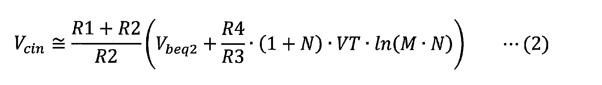
上式において、Vbeq2…Q2のベース-エミッタ間電位差、VT…VT=kT/qで表され、k:ボルツマン定数、T:温度、q:電荷素量であり、温度Ta=27℃のときVT=0.026Vである。また、M…Q1とQ2のエミッタ面積比(Q1:Q2=M:1(M>1))、N…M6とM8のゲート幅の比(M6:M8=1:N(N>1))である。トランジスタM6、M8のゲート幅の比Nは、例えばN=1.5~2.0程度であり、カレントミラー回路の特性ばらつき、温度特性等を考慮し、クランプ電圧Vcinが解除電圧Vrinよりも常に高い電圧となるように設定する。 In the above equation, the base-emitter potential difference of Vbeq2...Q2 is expressed as VT...VT=kT/q, where k: Boltzmann constant, T: temperature, q: elementary charge, and when temperature Ta=27°C, VT =0.026V. Also, M...emitter area ratio of Q1 and Q2 (Q1:Q2=M:1 (M>1)), N...ratio of gate widths of M6 and M8 (M6:M8=1:N (N>1)) It is. The ratio N of the gate widths of the transistors M6 and M8 is, for example, about N=1.5 to 2.0, and taking into consideration the characteristic variations of the current mirror circuit, temperature characteristics, etc., the clamp voltage Vcin is always higher than the release voltage Vrin. Set the voltage to be high.
図2は、図1の回路における動作特性の一例を示す特性図である。図2の例では、UVLO回路の解除電圧Vrinを2.7V、通常動作時の電源電圧(通常動作電圧)Vopを12~14Vとした場合の入力電圧Vinに対するトランジスタQ2のコレクタ電流IcQ2を示している。 FIG. 2 is a characteristic diagram showing an example of the operating characteristics of the circuit shown in FIG. The example in FIG. 2 shows the collector current IcQ2 of the transistor Q2 with respect to the input voltage Vin when the release voltage Vrin of the UVLO circuit is 2.7V and the power supply voltage during normal operation (normal operating voltage) Vop is 12 to 14V. There is.
入力電圧Vinが0Vから立ち上がり、解除電圧Vrinを超えて出力電圧がLowレベルからHighレベルに切り替わる。そして、入力電圧Vinがクランプ電圧Vcinに達すると、トランジスタQ1、Q2のベース電圧が所定値以下になるように制御されてベース電圧の上昇が抑えられ、コレクタ電流IcQ2の増加も抑制される。電源電圧の入力電圧Vinが通常動作電圧Vopの12~14Vとなる状態においても、コレクタ電流IcQ2は多く流れることなく、UVLO回路の消費電流を低減できる。 The input voltage Vin rises from 0V, exceeds the release voltage Vrin, and the output voltage switches from Low level to High level. When the input voltage Vin reaches the clamp voltage Vcin, the base voltages of the transistors Q1 and Q2 are controlled to be below a predetermined value, suppressing the increase in the base voltage and also suppressing the increase in the collector current IcQ2. Even in a state where the input voltage Vin of the power supply voltage is 12 to 14 V of the normal operating voltage Vop, the collector current IcQ2 does not flow much, and the current consumption of the UVLO circuit can be reduced.
本実施形態の構成では、UVLO回路以外からトランジスタQ1とQ2のベース電圧の上昇を抑えるクランプ回路の参照電圧を必要としないため、電源電圧が立ち上がる際の小さい電圧においても安定して回路を動作させることができる。また、クランプ回路となるトランジスタM10によるクランプ電圧Vcinを決めるための素子は、トランジスタM5、M6及びM8であり、UVLO回路の出力を反転させるトランジスタM4、M6及びM7と同種のトランジスタで構成される。これらのトランジスタは、UVLO回路の解除電圧Vrinの検出を行うNPN型トランジスタQ1、Q2のベース-エミッタ間電圧Vbeの電圧差を利用している。このとき、各トランジスタの特性ばらつきは同じ傾向を示すことになる。したがって、素子の特性のばらつきに関わらず、トランジスタQ1、Q2のベース電圧のクランプを開始するクランプ電圧Vcinを、確実にUVLO回路の解除電圧Vrin(出力端OUT_UVLOの出力電圧が切り替わる時の入力電圧)よりも高い電圧に設定できる。 The configuration of this embodiment does not require a reference voltage for the clamp circuit that suppresses the rise in the base voltage of transistors Q1 and Q2 from other than the UVLO circuit, so the circuit operates stably even at a small voltage when the power supply voltage rises. be able to. Further, the elements for determining the clamp voltage Vcin by the transistor M10 serving as the clamp circuit are transistors M5, M6, and M8, which are constructed of the same type of transistors as the transistors M4, M6, and M7 that invert the output of the UVLO circuit. These transistors utilize the voltage difference between the base-emitter voltage Vbe of the NPN transistors Q1 and Q2, which detects the release voltage Vrin of the UVLO circuit. At this time, the characteristic variations of each transistor show the same tendency. Therefore, regardless of variations in the characteristics of the elements, the clamp voltage Vcin that starts clamping the base voltages of the transistors Q1 and Q2 can be reliably set to the release voltage Vrin of the UVLO circuit (the input voltage when the output voltage of the output terminal OUT_UVLO is switched). Can be set to a higher voltage.
(第2の実施形態)
図3は、第2の実施形態の電圧検出回路の構成を示す図である。第2の実施形態は、図1に示した第1の実施形態における一部の構成を変更した例である。ここでは、第1の実施形態と異なる部分を中心に説明し、同様の構成及び動作については説明を省略する。
(Second embodiment)
FIG. 3 is a diagram showing the configuration of a voltage detection circuit according to the second embodiment. The second embodiment is an example in which a part of the configuration of the first embodiment shown in FIG. 1 is changed. Here, the description will focus on the parts that are different from the first embodiment, and the description of the similar configurations and operations will be omitted.
第2の実施形態の電圧検出回路は、カレントミラー回路を構成するトランジスタM1、M2のソース、及びトランジスタM3、M4、M5のソース、すなわちカレントミラー回路の電源入力部は、入力端VINと分離されて直接接続されない。入力端VINとトランジスタM1、M2、M3、M4、M5のソースとの間には、NMOS型のトランジスタM11(第3のMOSFET)が設けられ、トランジスタM11のドレインが入力端VINに接続され、ソースがトランジスタM1~M5のソースと接続される。トランジスタM11のゲートは、トランジスタM10のゲートと共に抵抗R5を介して入力端VINに接続される。第3のMOSFETであるトランジスタM11は、電圧入力端と第1カレントミラー回路及び第2カレントミラー回路の電源入力部とを分離する電源分離素子として機能する。その他の構成は第1の実施形態と同様である。 In the voltage detection circuit of the second embodiment, the sources of transistors M1 and M2 and the sources of transistors M3, M4, and M5 constituting the current mirror circuit, that is, the power input section of the current mirror circuit, are separated from the input terminal VIN. connection is not made directly. An NMOS transistor M11 (third MOSFET) is provided between the input terminal VIN and the sources of the transistors M1, M2, M3, M4, and M5, and the drain of the transistor M11 is connected to the input terminal VIN, and the source is connected to the sources of transistors M1 to M5. The gate of the transistor M11 and the gate of the transistor M10 are connected to the input terminal VIN via a resistor R5. The transistor M11, which is the third MOSFET, functions as a power isolation element that isolates the voltage input terminal from the power input portions of the first current mirror circuit and the second current mirror circuit. The other configurations are similar to the first embodiment.
上記構成において、入力電圧Vinの上昇に伴ってトランジスタQ1、Q2のベース電圧が上昇する際、入力電圧Vinがクランプ電圧Vcinを超えると、トランジスタQ1、Q2のベース電圧は所定値以下になるように制御される。このとき、トランジスタM1、M2、及びトランジスタM3、M4、M5のソース電圧も同様に、トランジスタM11によって所定値以下になるように制御され、ソース電圧の上昇が抑えられる。 In the above configuration, when the base voltages of transistors Q1 and Q2 increase as the input voltage Vin increases, when the input voltage Vin exceeds the clamp voltage Vcin, the base voltages of the transistors Q1 and Q2 are set to be below a predetermined value. controlled. At this time, the source voltages of the transistors M1, M2, and the transistors M3, M4, and M5 are similarly controlled by the transistor M11 to be equal to or lower than a predetermined value, thereby suppressing an increase in the source voltages.
図1に示した第1の実施形態では、入力端VINに高い電圧が印加される場合、トランジスタQ1、Q2及びトランジスタM1~M10もその高電圧に耐える高い耐圧の素子が必要となる。これに対し、第2の実施形態では、トランジスタQ1、Q2、トランジスタM1、M2、及びトランジスタM3、M4、M5の各素子に印加される電圧、すなわちUVLO回路の電源電圧は所定値以下に制御される。このため、素子レイアウトサイズが小さい低い耐圧の素子が使用可能であり、UVLO回路のレイアウト面積の縮小が可能となる。 In the first embodiment shown in FIG. 1, when a high voltage is applied to the input terminal VIN, the transistors Q1 and Q2 and the transistors M1 to M10 also need to be elements with high breakdown voltage to withstand the high voltage. In contrast, in the second embodiment, the voltages applied to each element of transistors Q1 and Q2, transistors M1 and M2, and transistors M3, M4, and M5, that is, the power supply voltage of the UVLO circuit, are controlled to be below a predetermined value. Ru. Therefore, an element with a small element layout size and low breakdown voltage can be used, and the layout area of the UVLO circuit can be reduced.
なお、電圧検出回路の入力部に他の電圧制限素子又は回路を追加して設け、入力端VINに印加される入力電圧Vinが通常動作時の電圧範囲を超えないようにクランプし、入力電圧Vinを所定値以下に制限する構成としてもよい。 Note that another voltage limiting element or circuit is additionally provided at the input section of the voltage detection circuit to clamp the input voltage Vin applied to the input terminal VIN so that it does not exceed the voltage range during normal operation. It may be configured to limit the value to a predetermined value or less.
上述したように、本実施形態の電圧検出回路は、UVLO回路におけるカレントミラー回路に第2出力部(トランジスタM5、M8)を設け、第2出力部の出力電流によってUVLO回路の入力部の分圧抵抗R1、R2に挿入された電流制限素子(トランジスタM10)の電流を制御する。これにより、UVLO回路の入力部の第1及び第2のトランジスタQ1、Q2のベース電圧が所定値以上に上がらないように制御する。 As described above, in the voltage detection circuit of this embodiment, the current mirror circuit in the UVLO circuit is provided with the second output section (transistors M5, M8), and the output current of the second output section divides the voltage at the input section of the UVLO circuit. The current of the current limiting element (transistor M10) inserted between the resistors R1 and R2 is controlled. Thereby, the base voltages of the first and second transistors Q1 and Q2 in the input section of the UVLO circuit are controlled so as not to rise above a predetermined value.
また、第2の実施形態の構成では、入力端VINに印加される電圧検出を行う部分である分圧抵抗R1、R2への入力電圧と、UVLO回路の電源電圧(カレントミラー回路の電源電圧)とを分離し、UVLO回路の電源電圧についても第2出力部の出力電流によって制御する。 In addition, in the configuration of the second embodiment, the input voltage to the voltage dividing resistors R1 and R2, which are the parts that detect the voltage applied to the input terminal VIN, and the power supply voltage of the UVLO circuit (power supply voltage of the current mirror circuit) The power supply voltage of the UVLO circuit is also controlled by the output current of the second output section.
このような構成により、通常動作時の入力電圧に対してバンドギャップ回路を構成する第1及び第2のトランジスタQ1、Q2のベース電圧を所定値以下に抑制し、UVLO回路の消費電流を抑制でき、回路全体の消費電力を低減することができる。このとき、自身の回路内における第2出力部のトランジスタM5、M8を流れる電流によって第1及び第2のトランジスタQ1、Q2のベース電圧を抑制しているため、素子の特性のばらつきの影響を受けることがない。例えば、素子の特性によってUVLO回路の解除電圧(検知電圧)Vrinが変動する場合、解除電圧Vrinに連動してクランプ電圧Vcinも変動する。このため、常に適切に解除電圧Vrinの検出と、消費電流の抑制とを実現できる。また、UVLO回路の電源電圧を所定値以下に抑制することにより、低い耐圧の素子によって電圧検出回路を構成可能となり、回路面積を縮小でき、電圧検出回路を搭載する装置の小型化を図れる。 With this configuration, the base voltage of the first and second transistors Q1 and Q2 that constitute the bandgap circuit can be suppressed to a predetermined value or less with respect to the input voltage during normal operation, and the current consumption of the UVLO circuit can be suppressed. , the power consumption of the entire circuit can be reduced. At this time, since the base voltages of the first and second transistors Q1 and Q2 are suppressed by the current flowing through the transistors M5 and M8 of the second output part in the own circuit, they are affected by variations in the characteristics of the elements. Never. For example, when the release voltage (detection voltage) Vrin of the UVLO circuit changes depending on the characteristics of the element, the clamp voltage Vcin also changes in conjunction with the release voltage Vrin. Therefore, it is possible to always appropriately detect the release voltage Vrin and suppress current consumption. Furthermore, by suppressing the power supply voltage of the UVLO circuit to a predetermined value or less, the voltage detection circuit can be constructed using elements with low breakdown voltage, the circuit area can be reduced, and the device equipped with the voltage detection circuit can be downsized.
本実施形態では、電圧検出回路において、第2カレントミラー回路12の第1出力部(トランジスタM4)に並列に設けられた第2出力部(トランジスタM5)と、第3カレントミラー回路13の第1出力部(トランジスタM7)に並列に設けられた第2出力部(トランジスタM8)とを有する。また、第1の抵抗R1と第2の抵抗R2との間に、第1の抵抗R1及び第2の抵抗R2に流れる電流を制限することにより、第1及び第2のトランジスタQ1、Q2のベース電圧を所定値以下にクランプするクランプ回路を構成する電流制限素子(トランジスタM10)を有する。また、第2カレントミラー回路12の第2出力部と第3カレントミラー回路13の第2出力部とが互いに接続された接続ノードに、入力電圧の変化に伴う第2カレントミラー回路12及び第3カレントミラー回路13の第2出力部の電圧の変化によって、クランプ回路の動作を制御するクランプ制御素子(トランジスタM9)を有する。
In the present embodiment, the voltage detection circuit includes a second output section (transistor M5) provided in parallel with the first output section (transistor M4) of the second
また、クランプ制御素子は、第2カレントミラー回路12の第2出力部と第3カレントミラー回路13の第2出力部との接続ノードにゲートが接続され、ソースが接地され、ドレインが第5の抵抗R5を介して電圧入力端VINに接続された第1のMOSFET(トランジスタM9)を有する。また、電流制限素子は、第1の抵抗R1にドレインが接続され、ソースが第1及び第2のトランジスタQ1、Q2のベースと第2の抵抗R2とに接続され、ゲートが第1のMOSFETのドレインと第5の抵抗R5とに接続された第2のMOSFET(トランジスタM10)を有する。第1のMOSFETは、入力電圧の変化に応じて第2のMOSFETのゲート電圧を制御し、第2のMOSFETは、ゲート電圧に応じてドレイン電流が変化し、第1の抵抗R1及び第2の抵抗R2に流れる電流を制限するものである。検出出力端OUT_UVLOの出力電圧が反転する第1の電圧値(UVLO回路の解除電圧Vrin)よりも大きい第2の電圧値(クランプ電圧Vcin)以上の電圧において、クランプ回路を動作させる。このとき、第3カレントミラー回路13の入力部(トランジスタM6)及び第1出力部(トランジスタM7)と、第2出力部(トランジスタM8)とのゲート幅の比は、1:N(N>1)である。
Further, the clamp control element has a gate connected to a connection node between the second output part of the second
上記構成において、電圧入力端VINの入力電圧Vinが0Vから上昇していき、解除電圧Vrinに達するとトランジスタM4のドレイン電流の方がトランジスタM7より大きくなり、検出出力端OUT_UVLOの出力電圧が反転することによって、入力電圧の立ち上がりを検出する。この時点では、トランジスタM5、M6、M7のドレイン電流よりトランジスタM8の方が大きくなっている。そして、入力電圧Vinがさらに上昇してクランプ電圧Vcinに達すると、トランジスタM5のドレイン電流の方がトランジスタM8より大きくなり、第1のMOSFET(トランジスタM9)がオンして第2のMOSFET(トランジスタM10)のドレイン電流を制限し、結果として第1及び第2のトランジスタQ1、Q2のベース電圧が所定値以下に抑制される。これにより、第1の抵抗R1及び第2の抵抗R2に流れる電流が制限され、消費電流が低減される。 In the above configuration, the input voltage Vin at the voltage input terminal VIN increases from 0V, and when it reaches the release voltage Vrin, the drain current of the transistor M4 becomes larger than that of the transistor M7, and the output voltage at the detection output terminal OUT_UVLO is inverted. By this, the rise of the input voltage is detected. At this point, the drain current of transistor M8 is larger than that of transistors M5, M6, and M7. Then, when the input voltage Vin further increases and reaches the clamp voltage Vcin, the drain current of the transistor M5 becomes larger than that of the transistor M8, the first MOSFET (transistor M9) is turned on, and the second MOSFET (transistor M10) is turned on. ), and as a result, the base voltages of the first and second transistors Q1 and Q2 are suppressed to below a predetermined value. This limits the current flowing through the first resistor R1 and the second resistor R2, reducing current consumption.
また、電圧検出回路において、電圧入力端VINと第1カレントミラー回路11及び第2カレントミラー回路12の電源入力部との間に、第1カレントミラー回路11及び第2カレントミラー回路12の電源入力部を分離する電源分離素子(トランジスタM11)をさらに有する。電源分離素子は、電圧入力端VINにドレインが接続され、ソースが第1カレントミラー回路11及び第2カレントミラー回路12の電源入力部に接続され、ゲートが第2のMOSFETのゲートと共に第1のMOSFETのドレイン及び第5の抵抗R5に接続された第3のMOSFET(トランジスタM11)を有する。これにより、電源分離素子によって電圧入力端VINと第1カレントミラー回路11及び第2カレントミラー回路12の電源入力部とを分離し、第1カレントミラー回路11及び第2カレントミラー回路12に印加される電源電圧が所定値以下に抑制される。このため、低い耐圧の素子によって電圧検出回路を構成可能となる。
In the voltage detection circuit, the power input terminal of the first
以上、図面を参照しながら各種の実施形態について説明したが、本発明はかかる例に限定されないことは言うまでもない。当業者であれば、特許請求の範囲に記載された範疇内において、各種の変更例又は修正例に想到し得ることは明らかであり、それらについても当然に本発明の技術的範囲に属するものと了解される。また、本発明の趣旨を逸脱しない範囲において、上記実施形態における各構成要素を任意に組み合わせてもよい。 Although various embodiments have been described above with reference to the drawings, it goes without saying that the present invention is not limited to such examples. It is clear that those skilled in the art can come up with various changes or modifications within the scope of the claims, and these naturally fall within the technical scope of the present invention. Understood. Further, each component in the above embodiments may be arbitrarily combined without departing from the spirit of the present invention.
本発明は、電圧検出回路における消費電力を低減することが可能となる効果を有し、例えばUVLO回路等において所定電圧を検出する電圧検出回路に有用である。 INDUSTRIAL APPLICATION This invention has the effect of being able to reduce the power consumption in a voltage detection circuit, and is useful for the voltage detection circuit which detects a predetermined voltage, for example in a UVLO circuit etc.
Q1、Q2:トランジスタ(NPN型)
M1、M2、M3、M4、M5:トランジスタ(PMOS型)
M6、M7、M8、M9、M10、M11:トランジスタ(NMOS型)
R1、R2、R3、R4、R5:抵抗
VIN:入力端(電圧入力端)
OUT_UVLO:出力端(検出出力端)
11:第1カレントミラー回路
12:第2カレントミラー回路
13:第3カレントミラー回路
Q1, Q2: Transistor (NPN type)
M1, M2, M3, M4, M5: Transistor (PMOS type)
M6, M7, M8, M9, M10, M11: Transistor (NMOS type)
R1, R2, R3, R4, R5: Resistor VIN: Input terminal (voltage input terminal)
OUT_UVLO: Output end (detection output end)
11: First current mirror circuit 12: Second current mirror circuit 13: Third current mirror circuit
Claims (5)
前記第1の抵抗と前記第2の抵抗との間に互いにベースが接続され、バンドギャップ回路を構成する第1のトランジスタ及び第2のトランジスタと、を有し、
前記第1のトランジスタのコレクタに第1カレントミラー回路の入力部の一方が接続され、前記第1カレントミラー回路の入力部の他方が前記電圧入力端に接続され、
前記第2のトランジスタのコレクタに第2カレントミラー回路の入力部の一方が接続され、前記第2カレントミラー回路の入力部の他方が前記電圧入力端に接続され、
前記第1カレントミラー回路の出力部に第3カレントミラー回路の入力部の一方が接続され、前記第3カレントミラー回路の入力部の他方が接地され、
前記第1のトランジスタのエミッタが第3の抵抗及び第4の抵抗を介して接地され、前記第2のトランジスタのエミッタが前記第3の抵抗と前記第4の抵抗の接続ノードに接続されて前記第4の抵抗を介して接地された差動入力回路部と、
前記第2カレントミラー回路の第1出力部と前記第3カレントミラー回路の第1出力部とが互いに接続された接続ノードに設けられる検出出力端と、を有し、
前記入力電圧の変化に伴い、前記第2カレントミラー回路及び前記第3カレントミラー回路の第1出力部の電圧が変化することによって、前記入力電圧が所定の電圧値以上、又は所定の電圧値以下になったことを検出する電圧検出回路であって、
前記第2カレントミラー回路の第1出力部に並列に設けられた第2カレントミラー回路の第2出力部と、
前記第3カレントミラー回路の第1出力部に並列に設けられた第3カレントミラー回路の第2出力部と、
前記第1の抵抗と前記第2の抵抗との間に設けられ、前記第1の抵抗及び前記第2の抵抗に流れる電流を制限することにより、前記第1及び第2のトランジスタのベース電圧を所定値以下にクランプするクランプ回路を構成する電流制限素子と、
前記第2カレントミラー回路の第2出力部と前記第3カレントミラー回路の第2出力部とが互いに接続された接続ノードにゲートが接続され、ソースが接地され、ドレインが第5の抵抗を介して前記電圧入力端に接続された第1のMOSFETを有し、前記入力電圧の変化に伴う前記第2カレントミラー回路及び前記第3カレントミラー回路の第2出力部の電圧の変化によって、前記クランプ回路の動作を制御するクランプ制御素子と、を有する、
電圧検出回路。 a first resistor and a second resistor that divide the input voltage applied to the voltage input terminal;
a first transistor and a second transistor whose bases are connected to each other between the first resistor and the second resistor and configure a bandgap circuit;
One of the input parts of the first current mirror circuit is connected to the collector of the first transistor, and the other input part of the first current mirror circuit is connected to the voltage input terminal,
One of the input parts of the second current mirror circuit is connected to the collector of the second transistor, and the other input part of the second current mirror circuit is connected to the voltage input terminal,
One of the input parts of the third current mirror circuit is connected to the output part of the first current mirror circuit, and the other input part of the third current mirror circuit is grounded,
The emitter of the first transistor is grounded via a third resistor and a fourth resistor, and the emitter of the second transistor is connected to a connection node between the third resistor and the fourth resistor. a differential input circuit section grounded via a fourth resistor;
a detection output terminal provided at a connection node where the first output section of the second current mirror circuit and the first output section of the third current mirror circuit are connected to each other;
As the input voltage changes, the voltages at the first output portions of the second current mirror circuit and the third current mirror circuit change, so that the input voltage is greater than or equal to a predetermined voltage value or less than or equal to a predetermined voltage value. A voltage detection circuit that detects when
a second output section of a second current mirror circuit provided in parallel with the first output section of the second current mirror circuit;
a second output section of a third current mirror circuit provided in parallel with the first output section of the third current mirror circuit;
The base voltage of the first and second transistors is reduced by providing between the first resistor and the second resistor, and limiting the current flowing through the first resistor and the second resistor. a current limiting element that constitutes a clamp circuit that clamps the current below a predetermined value;
A gate is connected to a connection node where a second output part of the second current mirror circuit and a second output part of the third current mirror circuit are connected to each other, a source is grounded, and a drain is connected to a connection node through a fifth resistor. a first MOSFET connected to the voltage input terminal, and the clamp a clamp control element that controls the operation of the circuit;
Voltage detection circuit.
前記電流制限素子は、前記第1の抵抗にドレインが接続され、ソースが前記第1のトランジスタ及び前記第2のトランジスタのベースと前記第2の抵抗とに接続され、ゲートが前記第1のMOSFETのドレインと前記第5の抵抗とに接続された第2のMOSFETを有し、
前記第1のMOSFETは、前記入力電圧の変化に応じて前記第2のMOSFETのゲート電圧を制御し、前記第2のMOSFETは、ゲート電圧に応じてドレイン電流が変化し、前記第1の抵抗及び前記第2の抵抗に流れる電流を制限するものであり、前記検出出力端の出力電圧が反転する第1の電圧値よりも大きい第2の電圧値以上の電圧において前記クランプ回路を動作させる、
電圧検出回路。 The voltage detection circuit according to claim 1,
The current limiting element has a drain connected to the first resistor, a source connected to the bases of the first transistor and the second transistor, and the second resistor, and a gate connected to the first MOSFET. a second MOSFET connected to the drain of the transistor and the fifth resistor;
The first MOSFET controls the gate voltage of the second MOSFET according to the change in the input voltage, and the drain current of the second MOSFET changes according to the gate voltage, and the first MOSFET controls the gate voltage of the second MOSFET according to the change in the input voltage. and limiting the current flowing through the second resistor, and operating the clamp circuit at a voltage equal to or higher than a second voltage value that is larger than the first voltage value at which the output voltage at the detection output terminal is inverted;
Voltage detection circuit.
前記第3カレントミラー回路の第1出力部及び第2出力部は、それぞれMOSFETにより構成され、2つのMOSFETのゲート幅の比は、1:N(N>1)である、
電圧検出回路。 The voltage detection circuit according to claim 1 or 2,
The first output section and the second output section of the third current mirror circuit are each constituted by a MOSFET, and the ratio of the gate widths of the two MOSFETs is 1:N (N>1).
Voltage detection circuit.
前記電圧入力端と前記第1カレントミラー回路及び前記第2カレントミラー回路の入力部の他方との間に設けられ、前記第1カレントミラー回路の入力部の他方及び前記第2カレントミラー回路の入力部の他方である電源入力部を分離する電源分離素子を、さらに有する、
電圧検出回路。 The voltage detection circuit according to claim 1,
provided between the voltage input terminal and the other of the input parts of the first current mirror circuit and the second current mirror circuit, the other of the input parts of the first current mirror circuit and the input of the second current mirror circuit; further comprising a power isolation element that isolates the power input section, which is the other of the sections ;
Voltage detection circuit.
前記クランプ制御素子は、前記第2カレントミラー回路の第2出力部と前記第3カレントミラー回路の第2出力部との接続ノードにゲートが接続され、ソースが接地され、ドレインが第5の抵抗を介して前記電圧入力端に接続された第1のMOSFETを有し、
前記電流制限素子は、前記第1の抵抗にドレインが接続され、ソースが前記第1及び第2のトランジスタのベースと前記第2の抵抗とに接続され、ゲートが前記第1のMOSFETのドレインと前記第5の抵抗とに接続された第2のMOSFETを有し、
前記電源分離素子は、前記電圧入力端にドレインが接続され、ソースが前記第1カレントミラー回路及び前記第2カレントミラー回路の入力部の他方に接続され、ゲートが前記第2のMOSFETのゲートと共に前記第1のMOSFETのドレイン及び前記第5の抵抗に接続された第3のMOSFETを有する、
電圧検出回路。 The voltage detection circuit according to claim 4,
The clamp control element has a gate connected to a connection node between the second output part of the second current mirror circuit and the second output part of the third current mirror circuit, a source connected to the ground, and a drain connected to the fifth resistor. a first MOSFET connected to the voltage input terminal via
The current limiting element has a drain connected to the first resistor, a source connected to the bases of the first and second transistors and the second resistor, and a gate connected to the drain of the first MOSFET. a second MOSFET connected to the fifth resistor;
The power supply separation element has a drain connected to the voltage input terminal, a source connected to the other of the input parts of the first current mirror circuit and the second current mirror circuit, and a gate connected to the gate of the second MOSFET. a third MOSFET connected to the drain of the first MOSFET and the fifth resistor;
Voltage detection circuit.
Priority Applications (1)
| Application Number | Priority Date | Filing Date | Title |
|---|---|---|---|
| JP2019085629A JP7364355B2 (en) | 2019-04-26 | 2019-04-26 | voltage detection circuit |
Applications Claiming Priority (1)
| Application Number | Priority Date | Filing Date | Title |
|---|---|---|---|
| JP2019085629A JP7364355B2 (en) | 2019-04-26 | 2019-04-26 | voltage detection circuit |
Publications (2)
| Publication Number | Publication Date |
|---|---|
| JP2020180932A JP2020180932A (en) | 2020-11-05 |
| JP7364355B2 true JP7364355B2 (en) | 2023-10-18 |
Family
ID=73023958
Family Applications (1)
| Application Number | Title | Priority Date | Filing Date |
|---|---|---|---|
| JP2019085629A Active JP7364355B2 (en) | 2019-04-26 | 2019-04-26 | voltage detection circuit |
Country Status (1)
| Country | Link |
|---|---|
| JP (1) | JP7364355B2 (en) |
Families Citing this family (1)
| Publication number | Priority date | Publication date | Assignee | Title |
|---|---|---|---|---|
| CN115328265B (en) * | 2021-05-11 | 2024-04-12 | 圣邦微电子(北京)股份有限公司 | Low-voltage UVLO circuit and method using sub-band gap voltage |
Citations (5)
| Publication number | Priority date | Publication date | Assignee | Title |
|---|---|---|---|---|
| JP2000065872A (en) | 1998-08-20 | 2000-03-03 | Fuji Electric Co Ltd | Voltage detection circuit |
| JP2007133533A (en) | 2005-11-09 | 2007-05-31 | Nec Electronics Corp | Reference voltage generation circuit |
| WO2012083781A1 (en) | 2010-12-22 | 2012-06-28 | Csmc Technologies Fab1 Co., Ltd | Voltage comparator |
| CN105021862A (en) | 2014-12-09 | 2015-11-04 | 北京中电华大电子设计有限责任公司 | Ultra-low power consumption voltage detection circuit |
| CN106855586A (en) | 2016-12-20 | 2017-06-16 | 宁波芯路通讯科技有限公司 | Low-voltage testing circuit |
-
2019
- 2019-04-26 JP JP2019085629A patent/JP7364355B2/en active Active
Patent Citations (5)
| Publication number | Priority date | Publication date | Assignee | Title |
|---|---|---|---|---|
| JP2000065872A (en) | 1998-08-20 | 2000-03-03 | Fuji Electric Co Ltd | Voltage detection circuit |
| JP2007133533A (en) | 2005-11-09 | 2007-05-31 | Nec Electronics Corp | Reference voltage generation circuit |
| WO2012083781A1 (en) | 2010-12-22 | 2012-06-28 | Csmc Technologies Fab1 Co., Ltd | Voltage comparator |
| CN105021862A (en) | 2014-12-09 | 2015-11-04 | 北京中电华大电子设计有限责任公司 | Ultra-low power consumption voltage detection circuit |
| CN106855586A (en) | 2016-12-20 | 2017-06-16 | 宁波芯路通讯科技有限公司 | Low-voltage testing circuit |
Also Published As
| Publication number | Publication date |
|---|---|
| JP2020180932A (en) | 2020-11-05 |
Similar Documents
| Publication | Publication Date | Title |
|---|---|---|
| TWI489239B (en) | Voltage regulator | |
| JP5516320B2 (en) | Semiconductor integrated circuit for regulator | |
| US7602162B2 (en) | Voltage regulator with over-current protection | |
| TWI437403B (en) | Voltage regulator | |
| US8269478B2 (en) | Two-terminal voltage regulator with current-balancing current mirror | |
| US7816897B2 (en) | Current limiting circuit | |
| TW201107920A (en) | Voltage regulator | |
| JP7354380B2 (en) | Electrical circuits that allow electronic components to start and shut down safely | |
| TW201931046A (en) | Circuit including bandgap reference circuit | |
| TWI672572B (en) | Voltage Regulator | |
| TWI818034B (en) | Backflow prevention circuit and power supply circuit | |
| JPH06324092A (en) | Hysteresis circuit and power supply system having hystresis circuit | |
| JP7364355B2 (en) | voltage detection circuit | |
| CN110045777B (en) | Reverse current prevention circuit and power supply circuit | |
| JP2009296714A (en) | Low-voltage detecting circuit and semiconductor integrated circuit for power supply control | |
| US20230246640A1 (en) | Wide voltage gate driver using low gate oxide transistors | |
| JP2022044215A (en) | Semiconductor integrated circuit for power supply | |
| JP2002074967A (en) | Step-down power-supply circuit | |
| JP4167122B2 (en) | Reference voltage generation circuit | |
| JP2021096554A (en) | Constant current circuit | |
| US20190288501A1 (en) | Semiconductor integrated circuit | |
| US20180095493A1 (en) | Enable signal generation circuit | |
| JP4249599B2 (en) | Reference voltage circuit | |
| KR102658159B1 (en) | Overheat protection circuit and semiconductor apparatus having the same | |
| US20210194368A1 (en) | Constant current circuit |
Legal Events
| Date | Code | Title | Description |
|---|---|---|---|
| A621 | Written request for application examination |
Free format text: JAPANESE INTERMEDIATE CODE: A621 Effective date: 20220408 |
|
| A977 | Report on retrieval |
Free format text: JAPANESE INTERMEDIATE CODE: A971007 Effective date: 20230228 |
|
| A131 | Notification of reasons for refusal |
Free format text: JAPANESE INTERMEDIATE CODE: A131 Effective date: 20230404 |
|
| A521 | Request for written amendment filed |
Free format text: JAPANESE INTERMEDIATE CODE: A523 Effective date: 20230512 |
|
| A131 | Notification of reasons for refusal |
Free format text: JAPANESE INTERMEDIATE CODE: A131 Effective date: 20230627 |
|
| A521 | Request for written amendment filed |
Free format text: JAPANESE INTERMEDIATE CODE: A523 Effective date: 20230714 |
|
| TRDD | Decision of grant or rejection written | ||
| A01 | Written decision to grant a patent or to grant a registration (utility model) |
Free format text: JAPANESE INTERMEDIATE CODE: A01 Effective date: 20230905 |
|
| A61 | First payment of annual fees (during grant procedure) |
Free format text: JAPANESE INTERMEDIATE CODE: A61 Effective date: 20231005 |
|
| R150 | Certificate of patent or registration of utility model |
Ref document number: 7364355 Country of ref document: JP Free format text: JAPANESE INTERMEDIATE CODE: R150 |