JP7354032B2 - Mask blank, transfer mask, and semiconductor device manufacturing method - Google Patents
Mask blank, transfer mask, and semiconductor device manufacturing method Download PDFInfo
- Publication number
- JP7354032B2 JP7354032B2 JP2020049162A JP2020049162A JP7354032B2 JP 7354032 B2 JP7354032 B2 JP 7354032B2 JP 2020049162 A JP2020049162 A JP 2020049162A JP 2020049162 A JP2020049162 A JP 2020049162A JP 7354032 B2 JP7354032 B2 JP 7354032B2
- Authority
- JP
- Japan
- Prior art keywords
- film
- light
- mask
- thin film
- shielding film
- Prior art date
- Legal status (The legal status is an assumption and is not a legal conclusion. Google has not performed a legal analysis and makes no representation as to the accuracy of the status listed.)
- Active
Links
- 238000012546 transfer Methods 0.000 title claims description 41
- 238000004519 manufacturing process Methods 0.000 title claims description 20
- 239000004065 semiconductor Substances 0.000 title claims description 20
- 239000010408 film Substances 0.000 claims description 328
- 239000000758 substrate Substances 0.000 claims description 103
- 239000010409 thin film Substances 0.000 claims description 96
- 238000000034 method Methods 0.000 claims description 35
- 230000002093 peripheral effect Effects 0.000 claims description 22
- 230000008033 biological extinction Effects 0.000 claims description 19
- 238000002834 transmittance Methods 0.000 claims description 10
- 230000010363 phase shift Effects 0.000 description 96
- 239000007789 gas Substances 0.000 description 60
- 238000004544 sputter deposition Methods 0.000 description 48
- 230000000873 masking effect Effects 0.000 description 38
- 239000000463 material Substances 0.000 description 31
- 239000011651 chromium Substances 0.000 description 26
- VYZAMTAEIAYCRO-UHFFFAOYSA-N Chromium Chemical compound [Cr] VYZAMTAEIAYCRO-UHFFFAOYSA-N 0.000 description 22
- 238000001312 dry etching Methods 0.000 description 21
- 229910052804 chromium Inorganic materials 0.000 description 20
- QVGXLLKOCUKJST-UHFFFAOYSA-N atomic oxygen Chemical compound [O] QVGXLLKOCUKJST-UHFFFAOYSA-N 0.000 description 17
- 239000001301 oxygen Substances 0.000 description 17
- 229910052760 oxygen Inorganic materials 0.000 description 17
- 238000005530 etching Methods 0.000 description 16
- 238000010438 heat treatment Methods 0.000 description 16
- 239000000460 chlorine Substances 0.000 description 15
- OKTJSMMVPCPJKN-UHFFFAOYSA-N Carbon Chemical compound [C] OKTJSMMVPCPJKN-UHFFFAOYSA-N 0.000 description 13
- 229910052799 carbon Inorganic materials 0.000 description 13
- IJGRMHOSHXDMSA-UHFFFAOYSA-N Atomic nitrogen Chemical compound N#N IJGRMHOSHXDMSA-UHFFFAOYSA-N 0.000 description 12
- MYMOFIZGZYHOMD-UHFFFAOYSA-N Dioxygen Chemical compound O=O MYMOFIZGZYHOMD-UHFFFAOYSA-N 0.000 description 12
- 230000000052 comparative effect Effects 0.000 description 12
- 238000013461 design Methods 0.000 description 12
- 229910001882 dioxygen Inorganic materials 0.000 description 12
- FFUAGWLWBBFQJT-UHFFFAOYSA-N hexamethyldisilazane Chemical compound C[Si](C)(C)N[Si](C)(C)C FFUAGWLWBBFQJT-UHFFFAOYSA-N 0.000 description 12
- 230000003287 optical effect Effects 0.000 description 11
- YCKRFDGAMUMZLT-UHFFFAOYSA-N Fluorine atom Chemical compound [F] YCKRFDGAMUMZLT-UHFFFAOYSA-N 0.000 description 10
- XUIMIQQOPSSXEZ-UHFFFAOYSA-N Silicon Chemical compound [Si] XUIMIQQOPSSXEZ-UHFFFAOYSA-N 0.000 description 10
- 229910052731 fluorine Inorganic materials 0.000 description 10
- 239000011737 fluorine Substances 0.000 description 10
- 229910052710 silicon Inorganic materials 0.000 description 10
- 239000010703 silicon Substances 0.000 description 10
- 239000002245 particle Substances 0.000 description 9
- XKRFYHLGVUSROY-UHFFFAOYSA-N Argon Chemical compound [Ar] XKRFYHLGVUSROY-UHFFFAOYSA-N 0.000 description 8
- ZAMOUSCENKQFHK-UHFFFAOYSA-N Chlorine atom Chemical compound [Cl] ZAMOUSCENKQFHK-UHFFFAOYSA-N 0.000 description 8
- 229910052801 chlorine Inorganic materials 0.000 description 8
- 239000010410 layer Substances 0.000 description 8
- 238000005546 reactive sputtering Methods 0.000 description 8
- 238000010894 electron beam technology Methods 0.000 description 7
- 238000005259 measurement Methods 0.000 description 7
- KZBUYRJDOAKODT-UHFFFAOYSA-N Chlorine Chemical compound ClCl KZBUYRJDOAKODT-UHFFFAOYSA-N 0.000 description 6
- 238000004140 cleaning Methods 0.000 description 6
- 239000000203 mixture Substances 0.000 description 6
- 238000012545 processing Methods 0.000 description 6
- GUVRBAGPIYLISA-UHFFFAOYSA-N tantalum atom Chemical compound [Ta] GUVRBAGPIYLISA-UHFFFAOYSA-N 0.000 description 6
- 238000011282 treatment Methods 0.000 description 6
- ZOKXTWBITQBERF-UHFFFAOYSA-N Molybdenum Chemical compound [Mo] ZOKXTWBITQBERF-UHFFFAOYSA-N 0.000 description 5
- 229910052786 argon Inorganic materials 0.000 description 5
- 230000015572 biosynthetic process Effects 0.000 description 5
- 238000011161 development Methods 0.000 description 5
- 238000000609 electron-beam lithography Methods 0.000 description 5
- 229910052750 molybdenum Inorganic materials 0.000 description 5
- 239000011733 molybdenum Substances 0.000 description 5
- 229910052757 nitrogen Inorganic materials 0.000 description 5
- 229910052756 noble gas Inorganic materials 0.000 description 5
- 238000004528 spin coating Methods 0.000 description 5
- 229910052715 tantalum Inorganic materials 0.000 description 5
- 229910052723 transition metal Inorganic materials 0.000 description 5
- 150000003624 transition metals Chemical class 0.000 description 5
- CURLTUGMZLYLDI-UHFFFAOYSA-N Carbon dioxide Chemical compound O=C=O CURLTUGMZLYLDI-UHFFFAOYSA-N 0.000 description 4
- MWUXSHHQAYIFBG-UHFFFAOYSA-N Nitric oxide Chemical compound O=[N] MWUXSHHQAYIFBG-UHFFFAOYSA-N 0.000 description 4
- VYPSYNLAJGMNEJ-UHFFFAOYSA-N Silicium dioxide Chemical compound O=[Si]=O VYPSYNLAJGMNEJ-UHFFFAOYSA-N 0.000 description 4
- 238000004833 X-ray photoelectron spectroscopy Methods 0.000 description 4
- 239000000470 constituent Substances 0.000 description 4
- 239000011521 glass Substances 0.000 description 4
- 229910052734 helium Inorganic materials 0.000 description 4
- 238000009434 installation Methods 0.000 description 4
- 238000004088 simulation Methods 0.000 description 4
- ZOXJGFHDIHLPTG-UHFFFAOYSA-N Boron Chemical compound [B] ZOXJGFHDIHLPTG-UHFFFAOYSA-N 0.000 description 3
- PXHVJJICTQNCMI-UHFFFAOYSA-N Nickel Chemical compound [Ni] PXHVJJICTQNCMI-UHFFFAOYSA-N 0.000 description 3
- KDLHZDBZIXYQEI-UHFFFAOYSA-N Palladium Chemical compound [Pd] KDLHZDBZIXYQEI-UHFFFAOYSA-N 0.000 description 3
- 229910052796 boron Inorganic materials 0.000 description 3
- 239000000428 dust Substances 0.000 description 3
- 239000001307 helium Substances 0.000 description 3
- SWQJXJOGLNCZEY-UHFFFAOYSA-N helium atom Chemical compound [He] SWQJXJOGLNCZEY-UHFFFAOYSA-N 0.000 description 3
- 238000003384 imaging method Methods 0.000 description 3
- 238000002156 mixing Methods 0.000 description 3
- 239000011368 organic material Substances 0.000 description 3
- 238000005477 sputtering target Methods 0.000 description 3
- 229910004298 SiO 2 Inorganic materials 0.000 description 2
- ATJFFYVFTNAWJD-UHFFFAOYSA-N Tin Chemical compound [Sn] ATJFFYVFTNAWJD-UHFFFAOYSA-N 0.000 description 2
- 229910002092 carbon dioxide Inorganic materials 0.000 description 2
- 239000001569 carbon dioxide Substances 0.000 description 2
- 238000012937 correction Methods 0.000 description 2
- 230000007547 defect Effects 0.000 description 2
- 238000001035 drying Methods 0.000 description 2
- 238000005516 engineering process Methods 0.000 description 2
- 238000001900 extreme ultraviolet lithography Methods 0.000 description 2
- 229910052738 indium Inorganic materials 0.000 description 2
- APFVFJFRJDLVQX-UHFFFAOYSA-N indium atom Chemical compound [In] APFVFJFRJDLVQX-UHFFFAOYSA-N 0.000 description 2
- 238000001755 magnetron sputter deposition Methods 0.000 description 2
- 229910052751 metal Inorganic materials 0.000 description 2
- 239000002184 metal Substances 0.000 description 2
- 239000010955 niobium Substances 0.000 description 2
- 238000000059 patterning Methods 0.000 description 2
- 238000000206 photolithography Methods 0.000 description 2
- 238000011160 research Methods 0.000 description 2
- 239000010948 rhodium Substances 0.000 description 2
- 239000002356 single layer Substances 0.000 description 2
- 230000003746 surface roughness Effects 0.000 description 2
- 229910052718 tin Inorganic materials 0.000 description 2
- 239000010936 titanium Substances 0.000 description 2
- ITWBWJFEJCHKSN-UHFFFAOYSA-N 1,4,7-triazonane Chemical compound C1CNCCNCCN1 ITWBWJFEJCHKSN-UHFFFAOYSA-N 0.000 description 1
- KJTLSVCANCCWHF-UHFFFAOYSA-N Ruthenium Chemical compound [Ru] KJTLSVCANCCWHF-UHFFFAOYSA-N 0.000 description 1
- 229910004541 SiN Inorganic materials 0.000 description 1
- 229910004535 TaBN Inorganic materials 0.000 description 1
- 229910004166 TaN Inorganic materials 0.000 description 1
- 229910004158 TaO Inorganic materials 0.000 description 1
- 229910003071 TaON Inorganic materials 0.000 description 1
- 229910004200 TaSiN Inorganic materials 0.000 description 1
- 229910010413 TiO 2 Inorganic materials 0.000 description 1
- RTAQQCXQSZGOHL-UHFFFAOYSA-N Titanium Chemical compound [Ti] RTAQQCXQSZGOHL-UHFFFAOYSA-N 0.000 description 1
- 239000006096 absorbing agent Substances 0.000 description 1
- 230000001154 acute effect Effects 0.000 description 1
- 239000000956 alloy Substances 0.000 description 1
- 229910045601 alloy Inorganic materials 0.000 description 1
- 239000005354 aluminosilicate glass Substances 0.000 description 1
- 238000000137 annealing Methods 0.000 description 1
- 238000013459 approach Methods 0.000 description 1
- 238000000576 coating method Methods 0.000 description 1
- 238000007796 conventional method Methods 0.000 description 1
- 239000013078 crystal Substances 0.000 description 1
- 230000002950 deficient Effects 0.000 description 1
- 238000000151 deposition Methods 0.000 description 1
- 230000008021 deposition Effects 0.000 description 1
- 238000010586 diagram Methods 0.000 description 1
- 229910001873 dinitrogen Inorganic materials 0.000 description 1
- 230000000694 effects Effects 0.000 description 1
- 229910052735 hafnium Inorganic materials 0.000 description 1
- VBJZVLUMGGDVMO-UHFFFAOYSA-N hafnium atom Chemical compound [Hf] VBJZVLUMGGDVMO-UHFFFAOYSA-N 0.000 description 1
- 229910052743 krypton Inorganic materials 0.000 description 1
- 230000014759 maintenance of location Effects 0.000 description 1
- 150000002739 metals Chemical class 0.000 description 1
- 229910052754 neon Inorganic materials 0.000 description 1
- 229910052759 nickel Inorganic materials 0.000 description 1
- 229910052758 niobium Inorganic materials 0.000 description 1
- GUCVJGMIXFAOAE-UHFFFAOYSA-N niobium atom Chemical compound [Nb] GUCVJGMIXFAOAE-UHFFFAOYSA-N 0.000 description 1
- 229910052763 palladium Inorganic materials 0.000 description 1
- 238000001552 radio frequency sputter deposition Methods 0.000 description 1
- 230000009257 reactivity Effects 0.000 description 1
- 229910052703 rhodium Inorganic materials 0.000 description 1
- MHOVAHRLVXNVSD-UHFFFAOYSA-N rhodium atom Chemical compound [Rh] MHOVAHRLVXNVSD-UHFFFAOYSA-N 0.000 description 1
- 229910052707 ruthenium Inorganic materials 0.000 description 1
- VSZWPYCFIRKVQL-UHFFFAOYSA-N selanylidenegallium;selenium Chemical compound [Se].[Se]=[Ga].[Se]=[Ga] VSZWPYCFIRKVQL-UHFFFAOYSA-N 0.000 description 1
- 229910052814 silicon oxide Inorganic materials 0.000 description 1
- 239000005361 soda-lime glass Substances 0.000 description 1
- 239000002344 surface layer Substances 0.000 description 1
- 229910052719 titanium Inorganic materials 0.000 description 1
- WFKWXMTUELFFGS-UHFFFAOYSA-N tungsten Chemical compound [W] WFKWXMTUELFFGS-UHFFFAOYSA-N 0.000 description 1
- 229910052721 tungsten Inorganic materials 0.000 description 1
- 239000010937 tungsten Substances 0.000 description 1
- LEONUFNNVUYDNQ-UHFFFAOYSA-N vanadium atom Chemical compound [V] LEONUFNNVUYDNQ-UHFFFAOYSA-N 0.000 description 1
- 229910052724 xenon Inorganic materials 0.000 description 1
Images


Classifications
-
- G—PHYSICS
- G03—PHOTOGRAPHY; CINEMATOGRAPHY; ANALOGOUS TECHNIQUES USING WAVES OTHER THAN OPTICAL WAVES; ELECTROGRAPHY; HOLOGRAPHY
- G03F—PHOTOMECHANICAL PRODUCTION OF TEXTURED OR PATTERNED SURFACES, e.g. FOR PRINTING, FOR PROCESSING OF SEMICONDUCTOR DEVICES; MATERIALS THEREFOR; ORIGINALS THEREFOR; APPARATUS SPECIALLY ADAPTED THEREFOR
- G03F1/00—Originals for photomechanical production of textured or patterned surfaces, e.g., masks, photo-masks, reticles; Mask blanks or pellicles therefor; Containers specially adapted therefor; Preparation thereof
- G03F1/26—Phase shift masks [PSM]; PSM blanks; Preparation thereof
- G03F1/32—Attenuating PSM [att-PSM], e.g. halftone PSM or PSM having semi-transparent phase shift portion; Preparation thereof
-
- G—PHYSICS
- G03—PHOTOGRAPHY; CINEMATOGRAPHY; ANALOGOUS TECHNIQUES USING WAVES OTHER THAN OPTICAL WAVES; ELECTROGRAPHY; HOLOGRAPHY
- G03F—PHOTOMECHANICAL PRODUCTION OF TEXTURED OR PATTERNED SURFACES, e.g. FOR PRINTING, FOR PROCESSING OF SEMICONDUCTOR DEVICES; MATERIALS THEREFOR; ORIGINALS THEREFOR; APPARATUS SPECIALLY ADAPTED THEREFOR
- G03F1/00—Originals for photomechanical production of textured or patterned surfaces, e.g., masks, photo-masks, reticles; Mask blanks or pellicles therefor; Containers specially adapted therefor; Preparation thereof
- G03F1/22—Masks or mask blanks for imaging by radiation of 100nm or shorter wavelength, e.g. X-ray masks, extreme ultraviolet [EUV] masks; Preparation thereof
- G03F1/24—Reflection masks; Preparation thereof
-
- G—PHYSICS
- G03—PHOTOGRAPHY; CINEMATOGRAPHY; ANALOGOUS TECHNIQUES USING WAVES OTHER THAN OPTICAL WAVES; ELECTROGRAPHY; HOLOGRAPHY
- G03F—PHOTOMECHANICAL PRODUCTION OF TEXTURED OR PATTERNED SURFACES, e.g. FOR PRINTING, FOR PROCESSING OF SEMICONDUCTOR DEVICES; MATERIALS THEREFOR; ORIGINALS THEREFOR; APPARATUS SPECIALLY ADAPTED THEREFOR
- G03F1/00—Originals for photomechanical production of textured or patterned surfaces, e.g., masks, photo-masks, reticles; Mask blanks or pellicles therefor; Containers specially adapted therefor; Preparation thereof
- G03F1/54—Absorbers, e.g. of opaque materials
-
- G—PHYSICS
- G03—PHOTOGRAPHY; CINEMATOGRAPHY; ANALOGOUS TECHNIQUES USING WAVES OTHER THAN OPTICAL WAVES; ELECTROGRAPHY; HOLOGRAPHY
- G03F—PHOTOMECHANICAL PRODUCTION OF TEXTURED OR PATTERNED SURFACES, e.g. FOR PRINTING, FOR PROCESSING OF SEMICONDUCTOR DEVICES; MATERIALS THEREFOR; ORIGINALS THEREFOR; APPARATUS SPECIALLY ADAPTED THEREFOR
- G03F1/00—Originals for photomechanical production of textured or patterned surfaces, e.g., masks, photo-masks, reticles; Mask blanks or pellicles therefor; Containers specially adapted therefor; Preparation thereof
- G03F1/60—Substrates
-
- G—PHYSICS
- G03—PHOTOGRAPHY; CINEMATOGRAPHY; ANALOGOUS TECHNIQUES USING WAVES OTHER THAN OPTICAL WAVES; ELECTROGRAPHY; HOLOGRAPHY
- G03F—PHOTOMECHANICAL PRODUCTION OF TEXTURED OR PATTERNED SURFACES, e.g. FOR PRINTING, FOR PROCESSING OF SEMICONDUCTOR DEVICES; MATERIALS THEREFOR; ORIGINALS THEREFOR; APPARATUS SPECIALLY ADAPTED THEREFOR
- G03F1/00—Originals for photomechanical production of textured or patterned surfaces, e.g., masks, photo-masks, reticles; Mask blanks or pellicles therefor; Containers specially adapted therefor; Preparation thereof
- G03F1/68—Preparation processes not covered by groups G03F1/20 - G03F1/50
- G03F1/80—Etching
Description
本発明は、マスクブランク、そのマスクブランクを用いて製造された転写用マスク、および上記の転写用マスクを用いた半導体デバイスの製造方法に関するものである。 The present invention relates to a mask blank, a transfer mask manufactured using the mask blank, and a method for manufacturing a semiconductor device using the above-described transfer mask.
一般に、半導体デバイスの製造工程では、フォトリソグラフィー法を用いて微細パターンの形成が行われている。また、この微細パターンの形成には通常何枚もの転写用マスクと呼ばれている基板が使用される。半導体デバイスのパターンを微細化するに当たっては、転写用マスクに形成されるマスクパターンの微細化に加え、フォトリソグラフィーで使用される露光光源の波長の短波長化が必要となる。半導体装置製造の際の露光光源としては、近年ではKrFエキシマレーザー(波長248nm)から、ArFエキシマレーザー(波長193nm)へと短波長化が進んでいる。 Generally, in the manufacturing process of semiconductor devices, fine patterns are formed using photolithography. Further, to form this fine pattern, usually a number of substrates called transfer masks are used. In order to miniaturize the pattern of a semiconductor device, in addition to miniaturizing the mask pattern formed on the transfer mask, it is necessary to shorten the wavelength of the exposure light source used in photolithography. In recent years, exposure light sources used in the manufacture of semiconductor devices have become shorter in wavelength, from KrF excimer lasers (wavelength: 248 nm) to ArF excimer lasers (wavelength: 193 nm).
近年、この転写用マスクの一つとして、ハーフトーン型位相シフトマスクと称される位相シフトマスクが開発されている。このハーフトーン型の位相シフトマスクは、透明基板上に形成するマスクパターンを、実質的に露光に寄与する強度の光を透過させる部分(光透過部)と、実質的に露光に寄与しない強度の光を透過させる部分(光半透過部)とで構成し、かつ、この光半透過部を通過する光の位相をシフトさせて、光半透過部を透過した光の位相が上記光透過部を透過した光の位相に対して実質的に反転する関係となるようにすることにより、光透過部と光半透過部との境界部近傍を透過した光が互いに打ち消しあうようにして境界部のコントラストを良好に保持できるようにしたものである。 In recent years, a phase shift mask called a halftone phase shift mask has been developed as one of these transfer masks. This halftone type phase shift mask has a mask pattern formed on a transparent substrate, with a part (light transmitting part) that transmits light with an intensity that substantially contributes to exposure, and a part (light transmitting part) with an intensity that does not substantially contribute to exposure. It consists of a part that transmits light (a light semi-transmissive part), and the phase of the light passing through the light semi-transmissive part is shifted so that the phase of the light that passes through the light semi-transmissive part is different from the light transmitting part. By creating a relationship that is substantially inverted with respect to the phase of the transmitted light, the contrast at the boundary is improved so that the light transmitted near the boundary between the light transmitting part and the light semi-transmitting part cancels each other out. It is designed to be able to maintain good retention.
しかしながら、露光に用いるレーザー光の波長が短波長化になることにより、レーザー光のエネルギーが大きくなるため、露光による光半透過膜へのダメージが大きくなってしまう。レーザー光に対する光半透過膜の耐久性を高めるためには、光半透過膜の膜を緻密化することが有効である。しかしながら、その反面、光半透過膜のシート抵抗が大きくなると、その上に形成したレジスト膜に対して電子線描画してパターニングするときに、光半透過膜に電荷がたまりチャージアップし、正確なパターン描画ができないという問題が発生した。
これに対し、特許文献1において、透明基板1上の周縁部に位相シフト膜2の存在しない露出部5を形成し、レジスト膜4を電子線描画しパターニングする際にチャージアップしない程度に導電性を有する材料からなる遮光膜を、露出部5及び位相シフト膜2を覆うように形成することで、チャージアップを抑制する技術が開示されている。
However, as the wavelength of the laser beam used for exposure becomes shorter, the energy of the laser beam increases, and therefore the damage to the light semi-transparent film due to exposure increases. In order to increase the durability of the light semi-transparent film against laser light, it is effective to make the light semi-transparent film dense. However, on the other hand, if the sheet resistance of the light semi-transparent film becomes large, when patterning is performed using electron beam lithography on the resist film formed on it, charges accumulate in the light semi-transparent film and charge up. A problem occurred where the pattern could not be drawn.
In contrast, in
上記のマスクブランクにおいて、遮光膜は、基板における面取り面や側面にわたる広い領域に形成されている。一方、パターンの微細化に伴い、ハードマスクとしても用いられる遮光膜は、膜厚40nm以下といったさらなる薄膜化が進んでいる。一般に、マスクブランクの遮光膜を含む薄膜は、スパッタリング法によって基板上に形成される。スパッタリング法による薄膜の形成時、基板の主表面に対するスパッタ粒子の入射角度に比べ、面取り面や側面に対するスパッタ粒子の入射角度は鋭角になる。このため、主表面に形成される薄膜の厚さに比べて、面取り面や側面に形成される薄膜の厚さは大幅に薄くなる。また、面取り面や側面に形成される薄膜の付着力は、主表面に形成される薄膜の付着力よりも弱い。これらの事情から、基板の面取り面や側面上に形成されている部分の遮光膜が剥がれやすく、マスクブランクのハンドリング時にその部分の遮光膜が剥がれて発塵しやすいという問題があった。この問題を解決するために、遮光膜をスパッタリング法で成膜するときに、その遮光膜の成膜領域(薄膜形成領域)の外縁が、基板の主表面の面取り面との稜線よりも内側であり、電子線描画装置にセットした時にアースピンを接触させる位置よりも外側になるように制御することを試みた。 In the mask blank described above, the light shielding film is formed in a wide area covering the chamfered surface and side surfaces of the substrate. On the other hand, as patterns become finer, light-shielding films, which are also used as hard masks, are becoming thinner, with a thickness of 40 nm or less. Generally, a thin film including a light shielding film of a mask blank is formed on a substrate by a sputtering method. When forming a thin film by sputtering, the angle of incidence of sputtered particles on a chamfered surface or side surface is more acute than the angle of incidence of sputtered particles on the main surface of a substrate. For this reason, the thickness of the thin film formed on the chamfered surface or side surface is significantly thinner than the thickness of the thin film formed on the main surface. Further, the adhesion force of the thin film formed on the chamfered surface or side surface is weaker than the adhesion force of the thin film formed on the main surface. Due to these circumstances, there has been a problem in that the light shielding film formed on the chamfered surface or side surface of the substrate tends to peel off, and when the mask blank is handled, the light shielding film on those parts easily peels off and generates dust. To solve this problem, when forming a light-shielding film by sputtering, the outer edge of the film-forming region (thin film formation region) of the light-shielding film is located inside the ridgeline of the chamfered surface of the main surface of the substrate. Therefore, we attempted to control the ground pin so that it is located outside of the contact position when it is set in an electron beam lithography system.
従来、基板の主表面上に形成される薄膜の領域を制御する場合、基板上に薄膜を形成したくない領域をマスキングするマスキングプレートを設置した状態でスパッタリングを行っている。すなわち、基板の主表面上の薄膜を形成したい領域(以下、これを「設計領域」という場合がある。)のみ露出させた状態でスパッタリングを行っている。このマスキングプレートを基板の主表面に接触させた状態でスパッタリングを行えば、基板の面取り面や側面に薄膜が回り込んで形成されることを回避することはできる。しかし、その場合、マスキングプレートと基板の主表面との接触により、基板に擦れや摩擦により傷や異物が発生してしまうという問題が生じる。このため、マスキングプレートを基板の主表面と非接触の状態で配置して、スパッタリングを行うことになる。そのスパッタリング時、ほとんどのスパッタ粒子は、基板の主表面に対して垂直な方向からある程度傾斜した方向で基板の主表面に入射する。また、スパッタ装置内には浮遊状態のスパッタ粒子も存在する。これらのことから、一定量のスパッタ粒子が基板の主表面とマスキングプレートとの隙間に回り込んで堆積することは避けがたい。すなわち、スパッタリングの終了後、基板の主表面上の設計領域には、所望の厚さで形成されるが、その設計領域の境界から少し外側にも厚さは薄いが薄膜が形成された状態になる。 Conventionally, when controlling the area of a thin film to be formed on the main surface of a substrate, sputtering is performed with a masking plate installed on the substrate to mask areas where the thin film is not desired to be formed. That is, sputtering is performed with only the area on the main surface of the substrate where a thin film is desired to be formed (hereinafter sometimes referred to as a "design area") exposed. By performing sputtering with this masking plate in contact with the main surface of the substrate, it is possible to avoid forming a thin film wrapping around the chamfered surface or side surface of the substrate. However, in that case, a problem arises in that the contact between the masking plate and the main surface of the substrate causes scratches and foreign matter on the substrate due to rubbing and friction. For this reason, sputtering is performed with the masking plate placed in a non-contact state with the main surface of the substrate. During sputtering, most of the sputtered particles are incident on the main surface of the substrate in a direction that is inclined to some extent from a direction perpendicular to the main surface of the substrate. Furthermore, floating sputtered particles also exist within the sputtering apparatus. For these reasons, it is inevitable that a certain amount of sputtered particles will enter and accumulate in the gap between the main surface of the substrate and the masking plate. In other words, after sputtering is completed, a desired thickness is formed in the designed area on the main surface of the substrate, but a thin film is also formed slightly outside the boundary of the designed area. Become.
特に、遮光膜のような導電性の高い薄膜を形成する場合、電子線描画装置等のアースピンが接触する位置よりも外側にまで薄膜が形成されていることが求められる。そのアースピンが接触する位置は、基板の主表面上の面取り面との稜線に近い位置になる場合が多い。このような薄膜を主表面上の面取り面との稜線に近い領域にまで形成する必要がある場合、マスキングプレートを設置するときの位置精度が低いと、スパッタ粒子が面取り面や側面にまで付着して薄膜が形成されてしまう恐れがある。すなわち、その薄膜形成領域を制御するためには、スパッタ装置のマスキングプレートの位置精度を高める必要がある。 In particular, when forming a highly conductive thin film such as a light-shielding film, it is required that the thin film be formed outside the position where an earth pin of an electron beam lithography device or the like comes into contact. The position where the ground pin makes contact is often a position close to the ridge line with the chamfered surface on the main surface of the substrate. If it is necessary to form such a thin film in an area close to the ridgeline of the chamfered surface on the main surface, if the positional accuracy when installing the masking plate is low, sputtered particles may adhere to the chamfered surface or side surfaces. Otherwise, a thin film may be formed. That is, in order to control the thin film formation region, it is necessary to improve the positional accuracy of the masking plate of the sputtering device.
そのマスキングプレートの位置精度を確認する手法として、実際に基板上にマスキングプレートを設置して遮光膜をスパッタリングで形成し、遮光膜が形成された領域を光学カメラで拡大して視認することを行った。その結果、遮光膜が形成されている領域と形成されていない領域との境界が確認しにくい場合があることがあり、問題となっていた。また、このような問題は、遮光膜に限定されず、基板上に薄膜を備える他の用途のマスクにおいても発生しうる。 As a method to check the positional accuracy of the masking plate, we actually set up the masking plate on the substrate, formed a light-shielding film by sputtering, and then visually checked the area where the light-shielding film was formed by magnifying it with an optical camera. Ta. As a result, it may be difficult to confirm the boundary between the area where the light shielding film is formed and the area where the light shielding film is not formed, which has been a problem. Further, such a problem is not limited to light shielding films, but may also occur in masks for other uses that include a thin film on a substrate.
本発明は、従来の課題を解決するためになされたものであり、基板上に薄膜を形成した場合において、薄膜が形成されている領域と形成されていない領域(基板が露出している領域)との境界を視認することが容易とすることを目的としている。また、これにより、基板の側面や面取り面に回り込んで薄膜が形成されることを回避するように、薄膜を形成するスパッタ装置に設けるマスキングプレートの位置調整を容易に行うことができるマスクブランクを提供することを目的としている。さらに、このマスクブランクを用いて製造される転写用マスクを提供することを目的としている。そして、本発明は、このような転写用マスクを用いた半導体デバイスの製造方法を提供することを目的としている。 The present invention was made to solve the conventional problems, and when a thin film is formed on a substrate, the area where the thin film is formed and the area where the thin film is not formed (area where the substrate is exposed) The purpose is to make it easy to visually recognize the boundaries between In addition, this makes it possible to easily adjust the position of the masking plate installed in the sputtering equipment that forms the thin film, so as to avoid forming the thin film by wrapping around the sides and chamfered surfaces of the substrate. is intended to provide. Furthermore, it is an object of the present invention to provide a transfer mask manufactured using this mask blank. An object of the present invention is to provide a method for manufacturing a semiconductor device using such a transfer mask.
前記の課題を達成するため、本発明は以下の構成を有する。
(構成1)
基板と薄膜とを備えるマスクブランクであって、
前記基板は、2つの主表面と側面を有し、前記2つの主表面と前記側面との間に面取り面が設けられ、
前記2つの主表面のうち一方の主表面は、該主表面の中心を含む内側領域と、該内側領域の外側の外周領域とを有し、
前記主表面の内側領域上に前記薄膜が設けられ、
波長400nmから700nmの光に対する前記主表面の外周領域の表面反射率Rsは、10%以下であり、
前記薄膜の膜厚が9nmから10nmの範囲内にある箇所のうちの1箇所での波長400nmから700nmの光に対する表面反射率をRfとしたとき、コントラスト比(Rf/Rs)は、3.0以上であることを特徴とするマスクブランク。
In order to achieve the above object, the present invention has the following configuration.
(Configuration 1)
A mask blank comprising a substrate and a thin film,
The substrate has two main surfaces and a side surface, and a chamfered surface is provided between the two main surfaces and the side surface,
One of the two main surfaces has an inner region including the center of the main surface and an outer peripheral region outside the inner region,
the thin film is provided on an inner region of the main surface;
The surface reflectance Rs of the outer peripheral region of the main surface with respect to light with a wavelength of 400 nm to 700 nm is 10% or less,
When the surface reflectance for light with a wavelength of 400 nm to 700 nm at one of the locations where the film thickness of the thin film is within the range of 9 nm to 10 nm is Rf, the contrast ratio (Rf/Rs) is 3.0. A mask blank characterized by the above.
(構成2)
前記波長400nmから700nmの光に対する、前記1箇所での表面反射率は、20%以上であることを特徴とする構成1記載のマスクブランク。
(構成3)
前記1箇所での波長400nmの光に対する表面反射率をRfB、前記1箇所での波長550nmの光に対する表面反射率をRfG、前記1箇所での波長700nmの光に対する表面反射率をRfRとしたとき、3つの前記表面反射率RfB、RfG、およびRfRの間で算出された標準偏差は、1.0以下であることを特徴とする構成1または2に記載のマスクブランク。
(Configuration 2)
The mask blank according to
(Configuration 3)
When the surface reflectance for light with a wavelength of 400 nm at the one location is RfB, the surface reflectance for light with a wavelength of 550 nm at the one location is RfG, and the surface reflectance for light with a wavelength of 700 nm at the one location is RfR. , the standard deviation calculated between the three surface reflectances RfB, RfG, and RfR is 1.0 or less, the mask blank according to
(構成4)
前記波長400nmから700nmの光に対する、前記薄膜の消衰係数kは、1.5以上であることを特徴とする構成1から3のいずれかに記載のマスクブランク。
(構成5)
前記薄膜の平均膜厚は、10nmよりも大きく60nm以下であることを特徴とする構成1から4のいずれかに記載のマスクブランク。
(Configuration 4)
4. The mask blank according to any one of
(Configuration 5)
5. The mask blank according to any one of
(構成6)
前記内側領域の外縁から前記一方の主表面の中心側に向かった内側の領域内において、該主表面と前記薄膜の間に中間膜が設けられていることを特徴とする構成1から5のいずれかに記載のマスクブランク。
(構成7)
前記中間膜は、ArFエキシマレーザーの露光光を1%以上の透過率で透過する光半透過膜であることを特徴とする構成6記載のマスクブランク。
(Configuration 6)
Any one of
(Configuration 7)
7. The mask blank according to configuration 6, wherein the intermediate film is a semi-transparent film that transmits exposure light from an ArF excimer laser with a transmittance of 1% or more.
(構成8)
構成1から5のいずれかに記載のマスクブランクにおける前記薄膜に転写パターンを備えてなることを特徴とする転写用マスク。
(構成9)
構成6または7に記載のマスクブランクにおける前記中間膜に転写パターンを備え、前記薄膜に遮光帯を含むパターンを備えてなることを特徴とする転写用マスク。
(Configuration 8)
A transfer mask, characterized in that the thin film in the mask blank according to any one of
(Configuration 9)
8. A transfer mask according to configuration 6 or 7, wherein the intermediate film is provided with a transfer pattern, and the thin film is provided with a pattern including a light-shielding band.
(構成10)
構成8または9に記載の転写用マスクを用い、半導体基板上のレジスト膜に転写パターンを露光転写する工程を備えることを特徴とする半導体デバイスの製造方法。
(Configuration 10)
A method for manufacturing a semiconductor device, comprising the step of exposing and transferring a transfer pattern to a resist film on a semiconductor substrate using the transfer mask according to Structure 8 or 9.
本発明のマスクブランクによれば、基板上に薄膜を形成した場合において、薄膜が形成されている領域と形成されていない領域との境界を視認することが容易となる。これにより、基板の側面や面取り面に回り込んで形成されることを回避するように、薄膜を形成するスパッタ装置に設けるマスキングプレートの位置調整を容易に行うことができる。 According to the mask blank of the present invention, when a thin film is formed on a substrate, it becomes easy to visually recognize the boundary between the region where the thin film is formed and the region where the thin film is not formed. Thereby, it is possible to easily adjust the position of the masking plate provided in the sputtering apparatus for forming a thin film so as to avoid forming the masking plate around the side surface or chamfered surface of the substrate.
以下、本発明の実施の形態について説明する前に、本発明に至った経緯について述べる。
本発明者らは、基板上に薄膜を形成した場合において、薄膜が形成されている領域と形成されていない領域(基板が露出している領域)との境界を視認することが容易であり、これにより、基板の側面や面取り面に回り込んで形成されることを回避するように、薄膜を形成するスパッタ装置に設けるマスキングプレートの位置調整を容易に行うことができるマスクブランクの構成について、鋭意研究を行った。
Hereinafter, before describing embodiments of the present invention, the circumstances leading to the present invention will be described.
The present inventors have discovered that when a thin film is formed on a substrate, it is easy to visually recognize the boundary between the region where the thin film is formed and the region where the thin film is not formed (the region where the substrate is exposed). As a result, we are working diligently to develop a mask blank configuration that can easily adjust the position of the masking plate installed in the sputtering equipment that forms thin films, so as to avoid forming the masking plate around the sides and chamfered surfaces of the substrate. conducted research.
上述の事情から、マスキングプレートを使用して薄膜をスパッタリングで形成しても、一定量のスパッタ粒子が基板の主表面とマスキングプレートとの隙間に回り込んで堆積することは避けがたい。すなわち、基板の主表面上の設計領域には、所望の厚さで形成されるが、その設計領域の境界から少し外側にも厚さは薄いが薄膜が形成された状態になる。その形成された薄膜は、主表面のマスキングプレートで覆われていない領域ではほぼ均一な厚さで形成される。しかし、スパッタ粒子がマスキングプレートと基板の主表面との隙間に入り込む影響により、その薄膜の端部は垂直な側壁を有する形状にはならない。すなわち、その薄膜の端部は、主表面の設計領域よりもある距離だけ外側にあり、設計領域よりも外側に形成された薄膜は、設計領域の境界の位置からその端部に向かって厚さが薄くなっていく形状になっている。 Due to the above-mentioned circumstances, even if a thin film is formed by sputtering using a masking plate, it is inevitable that a certain amount of sputtered particles will enter the gap between the main surface of the substrate and the masking plate and be deposited. That is, a desired thickness is formed in the design area on the main surface of the substrate, but a thin film is also formed slightly outside the boundary of the design area, albeit with a smaller thickness. The formed thin film has a substantially uniform thickness in the region of the main surface not covered by the masking plate. However, due to the influence of sputtered particles entering the gap between the masking plate and the main surface of the substrate, the ends of the thin film do not have vertical sidewalls. In other words, the edge of the thin film is a certain distance outside the design area of the main surface, and the thickness of the thin film formed outside the design area increases from the boundary of the design area to the edge. It has a shape that becomes thinner.
主表面上の設計領域の境界から薄膜の端部までの距離は、同じ設計仕様の2つのスパッタ装置の間でもその距離に差が生じることは避けがたい。同じスパッタ装置を用いた場合であっても、スパッタリング条件によって差が生じる。このため、実際に、マスキングプレートを設置した基板上に、設計した成膜条件で薄膜を形成し、薄膜の端部の位置を確認して、マスキングプレートの位置調整を行うことになる。本発明者らは、マスキングプレートの位置調整を行う頻度が比較的高いことを考慮し、薄膜の端部の識別にCCD等の撮像カメラで撮像した画像データを用いる方法(以下、この方法を「画像識別法」という場合がある。)を採用してみた。この画像識別法を用いる場合、主表面上の薄膜が形成されている領域と形成されていない領域(主表面が露出している領域)の境界を正確に検出することは困難である。この画像識別法では、薄膜が形成されていない領域で反射される光と、薄膜が形成されている領域で反射される光との間で、一定以上のコントラスト比が得られる箇所は、薄膜が存在していると識別される。この画像識別法で識別される薄膜が存在している領域の最外端の位置は、実際に薄膜が存在している領域の最外端の位置よりも少し内側になる。 It is inevitable that the distance from the boundary of the design area on the main surface to the end of the thin film will be different even between two sputtering apparatuses having the same design specifications. Even when the same sputtering equipment is used, differences occur depending on the sputtering conditions. For this reason, a thin film is actually formed on the substrate on which the masking plate is installed under the designed film forming conditions, and the position of the edge of the thin film is checked to adjust the position of the masking plate. The present inventors took into consideration the relatively high frequency of adjusting the position of the masking plate, and developed a method (hereinafter referred to as "this method") that uses image data captured by an imaging camera such as a CCD to identify the edge of a thin film. (Sometimes referred to as "image recognition method."). When using this image identification method, it is difficult to accurately detect the boundary between a region where a thin film is formed on the main surface and a region where it is not formed (a region where the main surface is exposed). In this image identification method, areas where a contrast ratio of more than a certain level is obtained between the light reflected in an area where a thin film is not formed and the light reflected in an area where a thin film is formed are identified by a thin film. identified as existing. The position of the outermost edge of the area where the thin film identified by this image identification method exists is slightly inside the position of the outermost edge of the area where the thin film actually exists.
本発明者らの鋭意研究の結果、薄膜の構成によっては、その画像識別法で識別される薄膜が存在している領域の最外端の位置と、実際に薄膜が存在している領域の最外端の位置との差が大きくなり、マスキングプレートの位置調整の精度が低くなる場合があることが判明した。そこで、本発明者らは、基板の主表面上にスパッタリングで形成された薄膜の設計領域から薄膜の端部までの薄膜の厚さの傾向を調べた上で、その薄膜の厚さと可視光(具体的には、波長400nmから700nmの光。以下、この波長帯の光を「可視光域の光」という場合がある。)に対する反射率との関係に着目し、さらに鋭意検討を行った。 As a result of intensive research by the present inventors, we have found that depending on the structure of the thin film, the outermost position of the area where the thin film is identified by the image recognition method and the outermost position of the area where the thin film actually exists may differ. It has been found that the difference from the position of the outer end becomes large, and the accuracy of position adjustment of the masking plate may become low. Therefore, the present inventors investigated the tendency of the thickness of the thin film formed by sputtering on the main surface of the substrate from the design area to the edge of the thin film, and determined the thickness of the thin film and the visible light ( Specifically, we focused on the relationship between the reflectance of light with a wavelength of 400 nm to 700 nm (hereinafter, light in this wavelength range may be referred to as "light in the visible light range"), and conducted further intensive studies.
まず、薄膜の厚さの傾向から、上記の画像取得法によって薄膜の厚さが最大で10nmの箇所で薄膜の存在を識別することができれば、実際に薄膜が存在している領域の最外端の位置との差は小さく、マスキングプレートの位置調整を高精度にできることを突き止めた。薄膜のその箇所で薄膜の存在が識別することを容易にするには、基板の主表面の薄膜が形成されていない外周領域での可視光域の光に対する表面反射率が低いことが望まれる。その表面反射率は10%以下であるとよいことが判明した。その上で、薄膜のその箇所で薄膜の存在が識別することを可能とするには、薄膜のその箇所での可視光域の光に対する表面反射率と、基板の主表面が露出している箇所での可視光域の光に対する表面反射率との間でのコントラスト比が3.0以上であることが望ましいことを突き止めた。さらに、薄膜の存在を識別しやすくするには、その薄膜の厚さが10nmから1nm薄くなっても、上記のコントラスト比を3.0以上に維持できることが望ましいことも判明した。 First, based on the tendency of the thickness of the thin film, if the presence of the thin film can be identified at a point where the thickness of the thin film is at most 10 nm using the image acquisition method described above, then the outermost edge of the area where the thin film actually exists It was found that the difference between the position of In order to easily identify the presence of a thin film at that location on the thin film, it is desirable that the surface reflectance for light in the visible light range be low in the outer peripheral region of the main surface of the substrate where the thin film is not formed. It has been found that the surface reflectance is preferably 10% or less. On top of that, in order to be able to identify the presence of a thin film at that location, it is necessary to determine the surface reflectance of the thin film at that location for light in the visible light range and the location where the main surface of the substrate is exposed. It has been found that it is desirable that the contrast ratio between the surface reflectance and the visible light range is 3.0 or more. Furthermore, it has been found that in order to easily identify the presence of a thin film, it is desirable to maintain the contrast ratio above 3.0 even if the thickness of the thin film is reduced from 10 nm to 1 nm.
すなわち、本発明のマスクブランクは、基板と薄膜とを備えるマスクブランクであって、前記基板は、2つの主表面と側面を有し、前記2つの主表面と前記側面との間に面取り面が設けられ、前記2つの主表面のうち一方の主表面は、該主表面の中心を含む内側領域と、該内側領域の外側の外周領域とを有し、前記主表面の内側領域上に前記薄膜が設けられ、波長400nmから700nmの光に対する前記主表面の外周領域の表面反射率Rsは10%以下であり、前記薄膜の膜厚が9nmから10nmの範囲内にある箇所のうちの1箇所での波長400nmから700nmの光に対する表面反射率をRfとしたとき、コントラスト比(Rf/Rs)は3.0以上であることを特徴とするものである。 That is, the mask blank of the present invention is a mask blank comprising a substrate and a thin film, the substrate having two main surfaces and a side surface, and a chamfered surface between the two main surfaces and the side surface. one of the two main surfaces has an inner region including the center of the main surface and a peripheral region outside the inner region, and the thin film is disposed on the inner region of the main surface. is provided, the surface reflectance Rs of the outer peripheral region of the main surface for light with a wavelength of 400 nm to 700 nm is 10% or less, and the thickness of the thin film is in one of the locations within the range of 9 nm to 10 nm. It is characterized in that the contrast ratio (Rf/Rs) is 3.0 or more, where Rf is the surface reflectance for light with a wavelength of 400 nm to 700 nm.
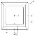
図1は、本発明の実施形態に係るマスクブランク100の構成を示す断面図である。図1に示す本発明のマスクブランク100は、透光性基板10上に、位相シフト膜20、遮光膜30、ハードマスク膜31がこの順に積層された構造を有する。
FIG. 1 is a cross-sectional view showing the configuration of a mask blank 100 according to an embodiment of the present invention. A
透光性基板10は、合成石英ガラスのほか、石英ガラス、アルミノシリケートガラス、ソーダライムガラス、低熱膨張ガラス(SiO2-TiO2ガラス等)などで形成することができる。これらの中でも、合成石英ガラスは、ArF露光光に対する透過率が高く、変形を起こしにくい十分な剛性も有するため、マスクブランクの透光性基板を形成する材料として特に好ましい。チャンバー(図示せず)内に収容される基板10は、2つの主表面11(11a、11b)と、側面12と、主表面11と側面12との境界部を面取り加工して形成された面取り面13とを有している。主表面11と面取り面13との境界は、主表面11側から見て、基板の側面12から0.5mm未満となっていることが好ましく、0.4mm以下となっているとより好ましい。
The light-transmitting
図2に示すように、この2つの主表面11のうち一方の主表面11aは、この主表面11aの中心17を含む内側領域14と、内側領域14の外側の外周領域15を有している。この内側領域14上に薄膜である遮光膜30が設けられる。外周領域15には、遮光膜30は実質的に形成されていない、すなわち主表面11aは実質的に露出している。遮光膜30が実質的に形成されていない状態、あるいは主表面11aが実質的に露出している状態には、遮光膜30を構成するスパッタ粒子がわずかに付着して1nm未満で堆積している状態も含まれる。その程度の堆積状態であれば、欠陥の要因にはなり難く、主表面11aが完全に露出している状態の表面反射率Rsとの間で実質的な差が生じない。なお、図2に示した内側領域14と外周領域15の境界線や中心17は、説明のために付された仮想的なものであり、実際の基板において必ずしも実際に付されているものではない点、念のため付記する。
As shown in FIG. 2, one of the two
内側領域14と外周領域15との境界線は、基板10の面取り面13と主表面11aとの境界から0.05mm以上で内側にあると好ましい。
また、基板10における、波長が400nmから700nmの光に対する、外周領域15の表面反射率Rsは、10%以下であることが好ましく、8%以下であるとより好ましく、7%以下であるとさらに好ましい。表面反射率Rsおよび後述の表面反射率Rfは、ともにCCD等の撮像カメラで撮影された画像データを基に測定することができる。外周領域15の表面反射率Rsが上記の範囲にすることで、薄膜の膜厚が9nmから10nmの範囲内にあるときの波長400nmから700nmの光に対する薄膜の表面反射率Rfとの間でのコントラスト比を3.0以上になるように調整しやすくなる。
The boundary line between the
Further, the surface reflectance Rs of the outer
本実施形態においては、図1に示されるように、内側領域14と外周領域15の境界から主表面11aの中心17側に向かった内側の領域内において、主表面11aと薄膜である遮光膜30の間に、中間膜である位相シフト膜20が設けられている。
位相シフト膜20は、ケイ素を含有する材料からなる。
位相シフト膜20は、ArFエキシマレーザーの露光光を1%以上の透過率で透過させる機能(透過率)と、位相シフト膜20を透過した前記露光光に対して位相シフト膜20の厚さと同じ距離だけ空気中を通過した露光光との間で150度以上210度以下の位相差を生じさせる機能とを有する光半透過膜であることが好ましい。また、位相シフト膜20の透過率は、1%以上であると好ましく、2%以上であるとより好ましい。位相シフト膜20の透過率は、30%以下であることが好ましく、20%以下であるとより好ましい。
In this embodiment, as shown in FIG. 1, in the inner region from the boundary between the
The
The
位相シフト膜20の厚さは80nm以下であることが好ましく、70nm以下であるとより好ましい。位相シフト膜20の厚さは50nm以上とすることが好ましい。アモルファスの材料で位相シフト膜20を形成しつつ、位相シフト膜20の位相差を150度以上とするためには50nm以上は必要なためである。
The thickness of the
位相シフト膜20において、前記の光学特性と膜の厚さに係る諸条件を満たすため、位相シフト膜の露光光(ArF露光光)に対する屈折率nは、1.9以上であると好ましく、2.0以上であるとより好ましい。また、位相シフト膜20の屈折率nは、3.1以下であると好ましく、2.7以下であるとより好ましい。位相シフト膜20のArF露光光に対する消衰係数kは、0.26以上であると好ましく、0.29以上であるとより好ましい。また、位相シフト膜20の消衰係数kは、0.62以下であると好ましく、0.54以下であるとより好ましい。
In the
なお、位相シフト膜20を含む薄膜の屈折率nと消衰係数kは、その薄膜の組成だけで決まるものではない。その薄膜の膜密度や結晶状態なども屈折率nや消衰係数kを左右する要素である。このため、反応性スパッタリングで薄膜を形成する時の諸条件を調整して、その薄膜が所望の屈折率nおよび消衰係数kとなるように形成する。位相シフト膜20を、上記の屈折率nと消衰係数kの範囲にするには、反応性スパッタリングで形成する際に、貴ガスと反応性ガス(酸素ガス、窒素ガス等)の混合ガスの比率を調整することが有効であるが、それだけに限られることではない。反応性スパッタリングで形成する際における成膜室内の圧力、スパッタターゲットに印加する電力、ターゲットと透光性基板10との間の距離等の位置関係など多岐に渡る。また、これらの成膜条件は成膜装置に固有のものであり、形成される位相シフト膜20が所望の屈折率nおよび消衰係数kになるように適宜調整されるものである。
Note that the refractive index n and extinction coefficient k of the thin film including the
マスクブランク100は、位相シフト膜20上に、薄膜である遮光膜30を備える。一般に、バイナリ型の転写用マスクでは、転写パターンが形成される領域(転写パターン形成領域)の外周領域は、露光装置を用いて半導体ウェハ上のレジスト膜に露光転写した際に外周領域を透過した露光光による影響をレジスト膜が受けないように、所定値以上の光学濃度(OD)を確保することが求められている。この点については、位相シフトマスクの場合も同じである。通常、位相シフトマスクを含む転写用マスクの外周領域では、ODが3.0以上あると望ましいとされており、少なくとも2.0よりも大きいことが必要とされている。位相シフト膜20は所定の透過率で露光光を透過する機能を有しており、位相シフト膜20だけでは所定値の光学濃度を確保することは困難である。このため、マスクブランク100を製造する段階で位相シフト膜20の上に、不足する光学濃度を確保するために遮光膜30を積層しておくことが必要とされる。このようなマスクブランク100の構成とすることで、位相シフトマスク200(図3参照)を製造する途上で、位相シフト効果を使用する領域(基本的に転写パターン形成領域)の遮光膜30を除去すれば、外周領域に所定値の光学濃度が確保された位相シフトマスク200を製造することができる。
The
また、遮光膜30は、位相シフト膜20に転写パターン(位相シフトパターン)を形成するためのフッ素系ガスによるドライエッチングのときにエッチングマスクとして機能する必要がある。このため、遮光膜30は、フッ素系ガスによるドライエッチングにおいて、位相シフト膜20に対して十分なエッチング選択性を有する材料を適用する必要がある。遮光膜30には、位相シフト膜20に形成すべき微細パターンを精度よく形成できることが求められる。遮光膜30の平均膜厚は60nm以下であることが好ましく、50nm以下であるとより好ましく、40nm以下であるとさらに好ましい。遮光膜30の膜厚が厚すぎると、形成すべき微細パターンを高精度に形成することができない。他方、遮光膜30は、上記のとおり要求される光学濃度を満たすことが求められる。このため、遮光膜30の平均膜厚は、内側領域14と外周領域15との境界となる端部領域を除いて、10nmより大きいことが求められ、15nm以上であることが好ましい。ここで、平均膜厚は、特に限定されるものではないが、遮光膜30が形成されている領域を、約55μm×約55μmのエリアに分割し、各エリアにおいて測定された膜厚の平均をとることで算出することができる。
Further, the
本実施形態において、薄膜である遮光膜30は、遮光膜30の膜厚が9nmから10nmの範囲内にある箇所のうちの1箇所での波長が400nmから700nmの光に対する表面反射率をRfとしたとき、コントラスト比(Rf/Rs)が3.0以上になるように構成している。これにより、薄膜である遮光膜30が形成されている領域と形成されていない領域との境界を識別することが容易となる。また、視認性の観点から、波長400nmから700nmの光に対する、上記の1箇所での表面反射率Rfは、20%以上であることが好ましい。
In this embodiment, the
上述の通り、上記の表面反射率Rfを定めている遮光膜30(薄膜)の箇所は、厳密には遮光膜30の最外端ではない。しかし、遮光膜30のその箇所の位置から最外端の位置までの差は小さく、これを基準にマスキングプレートの位置調整をすることは十分に可能である。
導電性確保の観点から、遮光膜30のシート抵抗値は、1kΩ/Square以下であると好ましく、0.5kΩ/Square以下であるとより好ましい。
As described above, the location of the light shielding film 30 (thin film) that determines the above-mentioned surface reflectance Rf is not strictly speaking the outermost end of the
From the viewpoint of ensuring conductivity, the sheet resistance value of the
遮光膜30は、膜厚が9nmから10nmの範囲内にある箇所のうちの1箇所での波長400nmの光に対する表面反射率をRfB、上記1箇所での波長550nmの光に対する表面反射率をRfG、上記1箇所での波長700nmの光に対する表面反射率をRfRとしたとき、3つの前記表面反射率RfB、RfG、およびRfRの間で算出された標準偏差は、1.0以下であると好ましい。CCD等の撮像カメラでの撮影された画像データのRGB値から比較的容易に得ることができる。上記3つの波長の光に対する各反射率の偏差が小さい方が、遮光膜30の存在をより視認しやすい。
The
視認性の観点から、波長が400nmから700nmの光に対する、遮光膜30の消衰係数kは、1.5以上であることが好ましく、2.0以上であることがより好ましい。また、上記の光に対する遮光膜30の消衰係数kは、4.0以下であることが好ましく、3.5以下であることがより好ましい。
遮光膜30は、単層構造および2層以上の積層構造のいずれも適用可能である。また、単層構造の遮光膜および2層以上の積層構造の遮光膜の各層は、膜または層の厚さ方向でほぼ同じ組成である構成であっても、層の厚さ方向で組成傾斜した構成であってもよい。
From the viewpoint of visibility, the extinction coefficient k of the
The
遮光膜30は、上記のコントラスト比の条件を満たす限り、どのような材料で形成してもよい。遮光膜30は、クロムを含有する材料で形成することが好ましい。遮光膜30を形成するクロムを含有する材料としては、クロム金属の他、クロム(Cr)に酸素(O)、窒素(N)、炭素(C)、ホウ素(B)およびフッ素(F)から選ばれる1つ以上の元素を含有する材料が挙げられる。一般に、クロム系材料は、塩素系ガスと酸素ガスの混合ガスでエッチングされるが、クロム金属はこのエッチングガスに対するエッチングレートがあまり高くない。塩素系ガスと酸素ガスの混合ガスのエッチングガスに対するエッチングレートを高める点を考慮すると、遮光膜30を形成する材料としては、クロムに酸素、窒素、炭素、ホウ素およびフッ素から選ばれる一以上の元素を含有する材料が好ましい。また、遮光膜30を形成するクロムを含有する材料にモリブデン、インジウムおよびスズのうち一以上の元素を含有させてもよい。モリブデン、インジウムおよびスズのうち一以上の元素を含有させることで、塩素系ガスと酸素ガスの混合ガスに対するエッチングレートをより速くすることができる。
The
遮光膜30は、クロムを含有するターゲットを用いた反応性スパッタリング法により、位相シフト膜20上に形成することができる。スパッタリング法としては、直流(DC)電源を用いたもの(DCスパッタリング)でも、高周波(RF)電源を用いたもの(RFスパッタリング)でもよい。またマグネトロンスパッタリング方式であっても、コンベンショナル方式であってもよい。DCスパッタリングの方が、機構が単純である点で好ましい。また、マグネトロンスパッタリング方式を用いた方が、成膜レートが速くなり、生産性が向上する点から好ましい。なお、成膜装置はインライン型でも枚葉型でも構わない。
The
遮光膜30を形成するときに使用するスパッタリングガスとしては、酸素を含まず炭素を含むガス(CH4、C2H4、C2H6等)と炭素を含まず酸素を含むガス(O2、O3等)と貴ガス(Ar、Kr、Xe、He、Ne等)とを含む混合ガス、炭素及び酸素を含むガス(CO2、CO等)と貴ガスとを含む混合ガス、あるいは貴ガスと炭素及び酸素を含むガスに、酸素を含まず炭素を含むガス(CH4、C2H4、C2H6等)及び炭素を含まず酸素を含むガスの少なくとも一方を含む混合ガスのうちのいずれかが好ましい。特に、スパッタリングガスとしてCO2と貴ガスとの混合ガスを用いると安全であり、CO2ガスは酸素ガスよりも反応性が低いが故に、チャンバー内の広範囲に均一にガスが回り込むことができ、形成される遮光膜30の膜質が均一になる点から好ましい。導入方法としては別々にチャンバー内に導入してもよいし、いくつかのガスをまとめて又は全てのガスを混合して導入してもよい。
The sputtering gases used when forming the
ターゲットの材料は、クロム単体だけでなくクロムが主成分であればよく、酸素、炭素のいずれかを含むクロム、又は酸素、炭素を組み合わせたものをクロムに添加したターゲットを用いてよい。 The material of the target may be not only chromium alone but also chromium as a main component, and chromium containing either oxygen or carbon, or a target in which a combination of oxygen and carbon is added to chromium may be used.
なお、本発明のマスクブランクは、図1に示したものに限定されるものではなく、位相シフト膜20と遮光膜30の間に別の膜(エッチングストッパー膜)を介するように構成してもよい。この場合においては、前記のクロムを含有する材料でエッチングストッパー膜を形成し、ケイ素を含有する材料あるいはタンタルを含有する材料で遮光膜30を形成する構成とすることが好ましい。
また、本発明のマスクブランクは、上述した位相シフトマスク用のマスクブランクに限定されるものではなく、バイナリマスク用のマスクブランクにも適用することができる。この場合のマスクブランクは、透光性基板10の主表面11aと遮光膜30との間に位相シフト膜20を設けない構成になる。また、遮光膜30のみで上記の所定の光学濃度を確保されている。このようなマスクブランクの遮光膜30に転写パターンを形成することで、バイナリマスク(転写用マスク)を形成することができる。
また、本発明のマスクブランクは、EUVリソグラフィ(Extreme Ultraviolet Lithography)用の反射型マスクブランクであってもよい。この場合においては、吸収体膜を本実施形態における薄膜で構成することが好ましい。
Note that the mask blank of the present invention is not limited to that shown in FIG. Good too. In this case, it is preferable to form the etching stopper film with the above-mentioned chromium-containing material, and to form the light-shielding
Further, the mask blank of the present invention is not limited to the above-mentioned mask blank for a phase shift mask, but can also be applied to a mask blank for a binary mask. The mask blank in this case has a configuration in which the
Further, the mask blank of the present invention may be a reflective mask blank for EUV lithography (Extreme Ultraviolet Lithography). In this case, it is preferable that the absorber film is made of the thin film of this embodiment.
遮光膜30を形成するケイ素を含有する材料には、遷移金属を含有させてもよく、遷移金属以外の金属元素を含有させてもよい。遮光膜30に形成されるパターンは、基本的に外周領域の遮光帯パターンであり、転写用パターン領域に比べてArF露光光の積算照射量が少ないことや、この外周領域に微細パターンが配置されていることは稀であり、ArF耐光性が低くても実質的な問題が生じにくいためである。また、遮光膜30に遷移金属を含有させると、含有させない場合に比べて遮光性能が大きく向上し、遮光膜30の厚さを薄くすることが可能となるためである。遮光膜30に含有させる遷移金属としては、モリブデン(Mo)、タンタル(Ta)、タングステン(W)、チタン(Ti)、クロム(Cr)、ハフニウム(Hf)、ニッケル(Ni)、バナジウム(V)、ジルコニウム(Zr)、ルテニウム(Ru)、ロジウム(Rh)、ニオブ(Nb)、パラジウム(Pd)等のいずれか1つの金属またはこれらの金属の合金が挙げられる。
The silicon-containing material that forms the
マスクブランク100において、遮光膜30をエッチングするときに用いられるエッチングガスに対してエッチング選択性を有する材料で形成されたハードマスク膜31を遮光膜30の上にさらに積層させた構成としてもよい。図1に示されるように、ハードマスク膜31は、遮光膜30よりも内側の領域に形成されるため、遮光膜30とレジスト膜との導電性の確保において支障はない。ハードマスク膜31は、その直下の遮光膜30にパターンを形成するドライエッチングが終わるまでの間、エッチングマスクとして機能することができるだけの膜の厚さがあれば十分であり、基本的に光学濃度の制限を受けない。このため、ハードマスク膜31の厚さは遮光膜30の厚さに比べて大幅に薄くすることができる。そして、有機系材料のレジスト膜は、このハードマスク膜にパターンを形成するドライエッチングが終わるまでの間、エッチングマスクとして機能するだけの膜の厚さがあれば十分であるので、従来よりも大幅に厚さを薄くすることができる。レジスト膜の薄膜化は、レジスト解像度の向上とパターン倒れ防止に効果があり、微細化要求に対応していく上で極めて重要である。
In the mask blank 100, a
このハードマスク膜31は、遮光膜30がクロムを含有する材料で形成されている場合は、前記のケイ素を含有する材料で形成されることが好ましい。なお、この場合のハードマスク膜31は、有機系材料のレジスト膜との密着性が低い傾向があるため、ハードマスク膜31の表面をHMDS(Hexamethyldisilazane)処理を施し、表面の密着性を向上させることが好ましい。なお、この場合のハードマスク膜は、SiO2、SiN、SiON等で形成されるとより好ましい。
When the
また、遮光膜30がクロムを含有する材料で形成されている場合におけるハードマスク膜31の材料として、前記のほか、タンタルを含有する材料も適用可能である。この場合におけるタンタルを含有する材料としては、タンタル金属のほか、タンタルに窒素、酸素、ホウ素、炭素およびケイ素から選ばれる一以上の元素を含有させた材料などが挙げられる。たとえば、Ta、TaN、TaO、TaON、TaBN、TaBO、TaBON、TaCN、TaCO、TaCON、TaBCN、TaBOCN、TaSi、TaSiN、TaSiO、TaSiON、TaSiBN、TaSiBO、TaSiBON、TaSiC、TaSiCN、TaSiCO、TaSiCONなどが挙げられる。また、ハードマスク膜31は、遮光膜30がケイ素を含有する材料で形成されている場合、前記のクロムを含有する材料で形成されることが好ましい。
Further, in addition to the above-mentioned materials, a material containing tantalum can be used as the material of the
マスクブランク100において、遮光膜30の表面(ハードマスク膜31が形成されている場合にはハードマスク膜31の表面)に接して、有機系材料のレジスト膜が形成されていてもよい。DRAM hp32nm世代に対応する微細パターンの場合、遮光膜30に形成すべき遮光パターンに、線幅が40nmのSRAF(Sub-Resolution Assist Feature)が設けられることがある。しかし、この場合でも上述のようにハードマスク膜31を設けたことによってレジスト膜の膜厚を抑えることができ、これによってこのレジスト膜で構成されたレジストパターンの断面アスペクト比を1:2.5と低くすることができる。したがって、レジスト膜の現像時、リンス時等にレジストパターンが倒壊や脱離することを抑制することができる。なお、レジスト膜は、膜厚が80nm以下であることがより好ましい。レジスト膜は、電子線描画露光用のレジストであると好ましく、さらにそのレジストが化学増幅型であるとより好ましい。
In the mask blank 100, a resist film of an organic material may be formed in contact with the surface of the light shielding film 30 (or the surface of the
以上の構成のマスクブランク100は、次のような手順で製造する。先ず、透光性基板10を用意する。この透光性基板10は、側面12及び主表面11が所定の表面粗さ(例えば、一辺が1μmの四角形の内側領域内において自乗平均平方根粗さRqが0.2nm以下)に研磨され、その後、所定の洗浄処理及び乾燥処理を施されたものである。
The mask blank 100 having the above configuration is manufactured by the following procedure. First, a
次に、この透光性基板10上に、スパッタリング法によって位相シフト膜20を形成する。位相シフト膜20を形成した後には、所定の加熱温度でのアニール処理を行う。次に、位相シフト膜20上に、スパッタリング法によって上記の遮光膜30を形成する。
Next, a
遮光膜30を形成するときに使用するマスキングプレートの要部を図4に示す。同図に示されるように、基板10は、その両端を基板保持部51によって位置決め保持される。そして、基板10の上方には、その周縁部を覆う遮蔽板52が設けられている。遮蔽板52は、基板10と非接触な状態を保ちつつ、基板10の主表面11aの中心17に対して接近または離間するように位置調整可能な状態で設けられている。これらの遮蔽板52の位置を調整することにより、スパッタリングターゲット50から供給される遮光膜材料が、基板10の周縁部に付着することを抑制することが可能となる。
FIG. 4 shows the main parts of the masking plate used when forming the
そして、遮光膜30上にスパッタリング法によって、上記のハードマスク膜31を形成する。スパッタリング法による各層の形成においては、各層を構成する材料を所定の組成比で含有するスパッタリングターゲット及びスパッタリングガスを用い、さらに必要に応じて上述の貴ガスと反応性ガスとの混合ガスをスパッタリングガスとして用いた形成を行う。この後、このマスクブランク100がレジスト膜を有するものである場合には、必要に応じてハードマスク膜31の表面に対してHMDS(Hexamethyldisilazane)処理を施す。そして、HMDS処理がされたハードマスク膜31の表面上に、スピンコート法等の塗布法によってレジスト膜を形成し、マスクブランク100を完成させる。
Then, the
この実施形態の転写用マスクである位相シフトマスク200は、マスクブランク100の位相シフト膜20に転写パターン(位相シフトパターン)20aが形成され、遮光膜30に遮光帯を含む遮光パターン30bが形成されていることを特徴としている。マスクブランク100にハードマスク膜が設けられている構成の場合、この位相シフトマスク200の作成途上でハードマスク膜31は除去される。
In the
本発明に係る位相シフトマスク200の製造方法は、前記のマスクブランク100を用いるものであり、ドライエッチングにより遮光膜30に転写パターンを形成する工程と、転写パターンを有する遮光膜30をマスクとするドライエッチングにより位相シフト膜20に転写パターンを形成する工程と、遮光帯パターンを有するレジスト膜(レジストパターン40b)をマスクとするドライエッチングにより遮光膜30に遮光パターン30bを形成する工程とを備えることを特徴としている。以下、図3に示す製造工程にしたがって、本発明の位相シフトマスク200の製造方法を説明する。
A method for manufacturing a
先ず、マスクブランク100のハードマスク膜31上にレジスト膜をスピン塗布法によって形成する。次に、そのレジスト膜に対して、位相シフト膜20に形成すべき第1のパターン(位相シフトパターン)を電子線で露光描画する。なお、このとき、レジスト膜が形成された遮光膜30には、図示しないアースピンが接触しており、レジスト膜と遮光膜30との間でアースが確保されている(図2におけるアースピン接地箇所16を参照)。これにより、露光描画の際におけるチャージアップを抑制することができる。その後、レジスト膜に対してPEB処理、現像処理、ポストベーク処理等の所定の処理を行い、位相シフトパターンに対応する第1のレジストパターン40aをレジスト膜に形成する(図3(a)参照)。
First, a resist film is formed on the
次に、レジストパターン40aをマスクとして、フッ素系ガスを用いてハードマスク膜31のドライエッチングを行い、第1のパターンであるハードマスクパターン31aをハードマスク膜31に形成する(図3(b)参照)。この後、レジストパターン40aを除去する。なお、ここで、レジストパターン40aを除去せず残存させたまま、遮光膜30のドライエッチングを行ってもよい。この場合では、遮光膜30のドライエッチングの際にレジストパターン40aが消失する。
Next, using the resist
次に、ハードマスクパターン31aをマスクとして、酸素含有塩素系ガスを用いたドライエッチングを行い、第1のパターンである遮光パターン30aを遮光膜30に形成する(図3(c)参照)。遮光膜30のドライエッチングにおける塩素系ガスと酸素ガスとの混合ガスの混合比率は、エッチング装置内でのガス流量比で、塩素系ガス:酸素ガス=10以上:1であることが好ましく、15以上:1であるとより好ましく、20以上:1であるとより好ましい。塩素系ガスの混合比率の高いエッチングガスを用いることにより、ドライエッチングの異方性を高めることができる。また、遮光膜30のドライエッチングにおいて、塩素系ガスと酸素ガスとの混合ガスの混合比率は、エッチングチャンバー内でのガス流量比で、塩素系ガス:酸素ガス=40以下:1であることが好ましい。
Next, using the
続いて、遮光パターン30aをマスクとして、フッ素系ガスを用いたドライエッチングを行い、第1のパターンである位相シフトパターン20aを位相シフト膜20に形成し、かつハードマスクパターン31aを除去する(図3(d)参照)。次に、遮光パターン30a上にレジスト膜をスピン塗布法によって形成する。そのレジスト膜に対して、遮光膜30に形成すべき第2のパターンである遮光パターンを電子線で露光描画する。その後、現像処理等の所定の処理を行い、遮光パターンに対応する第2のパターンであるレジストパターン40bを有するレジスト膜を形成する(図3(e)参照)。
Next, using the light-
次に、レジストパターン40bをマスクとして、塩素系ガスと酸素ガスの混合ガスを用いたドライエッチングを行い、第2のパターンである遮光パターン30bを遮光膜30に形成する(図3(f)参照)。さらに、レジストパターン40bを除去し、洗浄等の所定の処理を経て、位相シフトマスク200を得る(図3(g)参照)。
Next, using the resist
なお、上記の製造工程中のドライエッチングで使用される塩素系ガスとしては、Clが含まれていれば特に制限はない。たとえば、塩素系ガスとして、Cl2、SiCl2、CHCl3、CH2Cl2、CCl4、BCl3等があげられる。また、上記の製造工程中のドライエッチングで使用されるフッ素系ガスとしては、Fが含まれていれば特に制限はない。たとえば、フッ素系ガスとして、CHF3、CF4、C2F6、C4F8、SF6等があげられる。特に、Cを含まないフッ素系ガスは、ガラス基板に対するエッチングレートが比較的低いため、ガラス基板へのダメージをより小さくすることができる。 Note that there is no particular restriction on the chlorine-based gas used in the dry etching in the above manufacturing process as long as it contains Cl. For example, examples of the chlorine gas include Cl 2 , SiCl 2 , CHCl 3 , CH 2 Cl 2 , CCl 4 , and BCl 3 . Further, there is no particular restriction on the fluorine-based gas used in the dry etching in the above manufacturing process as long as it contains F. For example, examples of the fluorine gas include CHF 3 , CF 4 , C 2 F 6 , C 4 F 8 , SF 6 and the like. In particular, since a fluorine-based gas that does not contain C has a relatively low etching rate on a glass substrate, damage to the glass substrate can be further reduced.
本発明の位相シフトマスク200は、前記のマスクブランク100を用いて作製されたものである。このため、レジストに対するアースを確保することができるとともに、発塵を抑えることができるので、良好なパターン転写を行うことが可能となる。
The
本発明の半導体デバイスの製造方法は、前記の位相シフトマスク200または前記のマスクブランク100を用いて製造された位相シフトマスク200を用い、半導体基板上のレジスト膜に転写パターンを露光転写する工程を備えることを特徴としている。このため、この位相シフトマスク200を露光装置にセットし、その位相シフトマスク200の透光性基板1側からArF露光光を照射して転写対象物(半導体ウェハ上のレジスト膜等)へ露光転写を行っても、高い精度で転写対象物に所望のパターンを転写することができる。
The method for manufacturing a semiconductor device of the present invention includes a step of exposing and transferring a transfer pattern to a resist film on a semiconductor substrate using the
以下、実施例により、本発明の実施の形態をさらに具体的に説明する。
(実施例1)
[マスクブランクの製造]
図1を参照し、主表面の寸法が約152mm×約152mmで、厚さが約6.35mmの合成石英ガラスからなる透光性基板1を準備した。この透光性基板10は、主表面が所定の表面粗さ(Rqで0.2nm以下)に研磨され、その後、所定の洗浄処理及び乾燥処理が施されている。この透光性基板10は、2つの主表面11と4つの側面12を有し、主表面11と側面12の間に面取り面13を有している。面取り面13と主表面11との境界(稜線)は、主表面11側からみて、基板の側面12から0.4mmだけ中心17側の位置にある。この透光性基板10の主表面11aの複数個所において、波長が400nmから700nmの光に対する表面反射率Rsを測定したところ、いずれの領域においても7%以下(波長400nm:6.99%,波長550nm:6.75%,波長700nm:6.62%)であった。
Hereinafter, embodiments of the present invention will be described in more detail with reference to Examples.
(Example 1)
[Manufacture of mask blank]
Referring to FIG. 1, a light-transmitting
次に、枚葉式DCスパッタリング装置内に透光性基板10を設置し、モリブデン(Mo)とケイ素(Si)との混合焼結ターゲット(Mo:Si=11原子%:89原子%)を用い、アルゴン(Ar)、窒素(N2)及びヘリウム(He)の混合ガスをスパッタリングガスとする反応性スパッタリング(DCスパッタリング)により、透光性基板10上に、モリブデン、ケイ素及び窒素からなる位相シフト膜20を69nmの厚さで形成した。この位相シフト膜20を形成するスパッタリングのとき、図4に示したようなマスキングプレートを用いた。使用したマスキングプレートは、基板の中心を基準とする一辺が146mmの正方形の開口を有する。
Next, the
次に、この位相シフト膜20が形成された透光性基板10に対して、位相シフト膜20の膜応力を低減するため、及び表層に酸化層を形成するための加熱処理を行った。具体的には、加熱炉(電気炉)を用いて、大気中で加熱温度を450℃、加熱時間を1時間として、加熱処理を行った。位相シフト量測定装置(レーザーテック社製 MPM193)を用いて、加熱処理後の位相シフト膜20の波長193nmの光に対する透過率と位相差を測定したところ、透過率が6.0%、位相差が177.0度(deg)であった。
Next, the
次に、枚葉式DCスパッタリング装置内に位相シフト膜20が形成された透光性基板10を設置し、クロム(Cr)ターゲットを用いて、アルゴン(Ar)、二酸化炭素(CO2)及びヘリウム(He)の混合ガス雰囲気での反応性スパッタリング(DCスパッタリング)を行った。これにより、位相シフト膜20に接して、クロム、酸素及び炭素からなる遮光膜(CrOC膜)30を18nmの膜厚で形成した。この遮光膜30を形成するスパッタリングのときもマスキングプレートを用いた。ただし、ここで使用したマスキングプレートは、基板の中心を基準とする一辺が150mmの正方形の開口を有する(すなわち、設計領域は、一辺が150mmの正方形の領域。)ものである。基板の主表面11の一辺の大きさは、151.2mmであり、設計領域との間での裕度はかなり小さい。
Next, the light-transmitting
次に、上記遮光膜(CrOC膜)30が形成された透光性基板10に対して、加熱処理を施した。具体的には、ホットプレートを用いて、大気中で加熱温度を280℃、加熱時間を5分として、加熱処理を行った。加熱処理後、位相シフト膜20及び遮光膜30が積層された透光性基板10に対し、分光光度計(アジレントテクノロジー社製 Cary4000)を用い、位相シフト膜20と遮光膜30の積層構造のArFエキシマレーザーの光の波長(約193nm)における光学濃度を測定したところ、2.0を上回ることが確認できた。
Next, the light-transmitting
次に、遮光膜30が形成された透光性基板10の主表面11aの四隅のそれぞれに対し、CCDカメラを用いて拡大した画像データを取得した。取得した各画像データは、遮光膜30と主表面11aとの境界を視認することができた。ただし、その四隅の各画像データの中に、主表面11aが全て遮光膜30で覆われてしまっている個所が見つかった(遮光膜30が面取り面13まで回り込んでいる可能性がある。)。すなわち、マスキングプレートが適切な位置に配置できていないことが判明した。そこで、四隅の各画像データのそれぞれに対し、側面12を基準とし、主表面11aが露出している領域(遮光膜30が形成されていない領域)と遮光膜30が形成されている領域との境界までの距離をそれぞれ計測した。この結果から、スパッタリング時の透光性基板10の中心17とマスキングプレートの中心との間の差を算出し、マスキングプレートの設置位置の微調整を行った。
Next, enlarged image data was obtained using a CCD camera for each of the four corners of the
次に、別の透光性基板10を準備し、上記と同様の手順で、位相シフト膜20と遮光膜30をスパッタリングで形成した。さらに、上記と同様の手順で、遮光膜30が形成された透光性基板10の主表面11aの四隅の各画像データを取得した。そして、上記と同様の手順で、四隅の各画像データのそれぞれに対し、側面12を基準とし、主表面11aが露出している領域と遮光膜30が形成されている領域との境界までの距離をそれぞれ計測した。その結果、四隅のいずれにおいても、主表面11aが露出している領域と遮光膜30が形成されている領域との境界が視認できた。また、側面12を基準とする境界までの距離もほぼ同じになっていた。
Next, another
次に、主表面11aと遮光膜30の境界付近における膜厚プロファイルを接触式微細形状測定機(小坂研究所製 ET-4000)で測定した。その結果を、図5に示す。この結果から、主表面11a上の側面12から内側に向かって0.47mmから0.53mmの間の距離の位置から遮光膜30が形成され始めていることがわかった。また、上記の画像データから遮光膜30の厚さが9nmから10nmの間にある複数の測定箇所(箇所)の波長400nmから700nmの光に対する表面反射率Rfを測定したところ、平均23.65%であり、上記波長の範囲内の光に対する表面反射率Rfはいずれも20%以上であった。さらに、主表面11aの表面反射率Rsに対する、上記測定箇所での遮光膜30の表面反射率Rfのコントラスト比(Rf/Rs)を算出したところ、最小でも3.29であり、3.0以上となっていた。さらに、表面反射率Rfが最大(24.69%)の測定箇所での波長400nmの光に対する表面反射率RfBは、24.96%、波長550nmの光に対する表面反射率RfGは、25.06%、波長700nmの光に対する表面反射率RfRは、24.08%であった。3つの前記表面反射率RfB、RfG、およびRfRの間で算出された標準偏差は、0.441であり、1.0以下であった。
Next, the film thickness profile near the boundary between the
この遮光膜30が形成されている領域(すなわち内側領域14)を、55μm×55μmのエリアに分割し、各エリアにおいて測定された膜厚の平均をとることで、遮光膜30の平均膜厚を算出した。算出された遮光膜30の平均膜厚は、18nmであった。
The area in which the
次に、別の透光性基板10を準備し、上記と同様の手順で、位相シフト膜20をスパッタリングで形成し、微調整後のマスキングプレートの設置位置で遮光膜30をスパッタリングで形成した。次に、枚葉式DCスパッタリング装置内に、位相シフト膜20及び遮光膜30が積層された透光性基板10を設置し、ケイ素(Si)ターゲットを用い、アルゴン(Ar)及び一酸化窒素(NO)の混合ガス雰囲気での反応性スパッタリング(DCスパッタリング)により遮光膜30の上でありかつ遮光膜30の端部よりも内側に、ケイ素、窒素及び酸素からなるハードマスク膜31を5nmの厚さで形成した。このとき、基板の中心を基準とする一辺が146mmの正方形の開口を有するマスキングプレートを使用した。さらに所定の洗浄処理を施し、実施例1のマスクブランク100を製造した。
Next, another
別の透光性基板10の主表面11a上に同条件で遮光膜30のみを形成し、加熱処理を行ったものを準備した。その遮光膜30のシート抵抗値を測定したところ、0.246kΩ/Squareであり、0.5kΩ/Square以下であった。また、分光エリプソメーターを用いて、波長400nmから700nmの光に対する遮光膜30の屈折率nと消衰係数kを測定した。その結果、波長400nmの光に対する消衰係数kは2.33、波長550nmの光に対する消衰係数kは2.53、波長700nmの光に対する消衰係数kは3.01であり、2.0以上であることが確認できた。なお、波長400nmの光に対する屈折率nは2.52、波長550nmの光に対する屈折率nは2.96、波長700nmの光に対する屈折率nは3.57であった。
A light-shielding
さらに、その遮光膜30に対し、X線光電子分光法(XPS,RBS補正有り)で分析を行った。この結果、遮光膜30の透光性基板10側とは反対側の表面近傍の領域(表面から2nm程度の深さまでの領域)は、それ以外の領域よりも酸素含有量が多い組成傾斜部(酸素含有量が40原子%以上)を有することが確認できた。また、遮光膜30の組成傾斜部を除く領域における各構成元素の含有量は、平均値でCr:71原子%、O:14原子%、C:15原子%であることがわかった。さらに、遮光膜30の組成傾斜部を除く領域の厚さ方向における各構成元素の差は、いずれも3原子%以下であり、厚さ方向の組成傾斜は実質的にないことが確認できた。
Further, the
次に、この実施例1のマスクブランク100を用い、以下の手順で実施例1のハーフトーン型の位相シフトマスク200を製造した。最初に、ハードマスク膜31の表面にHMDS処理を施した。続いて、スピン塗布法によって、ハードマスク膜31の表面に接して、電子線描画用化学増幅型レジストからなるレジスト膜を膜厚80nmで形成した。次に、このレジスト膜に対して、位相シフト膜20に形成すべき位相シフトパターンである第1のパターンを電子線描画し、所定の現像処理及び洗浄処理を行い、第1のパターンを有するレジストパターン40aを形成した(図3(a)参照)。この電子線描画の際には、アースピン接地箇所16において、遮光膜30をアースピン(図示せず)に接触させていた。これにより、レジスト膜には所望の位置に電子線が描画され、所望のレジストパターン40aを形成することができた。
Next, using the
次に、レジストパターン40aをマスクとし、CF4ガスを用いたドライエッチングを行い、第1のパターンであるハードマスクパターン31aをハードマスク膜31に形成した(図3(b)参照)。
Next, using the resist
次に、レジストパターン40aを除去した。続いて、ハードマスクパターン31aをマスクとし、塩素ガス(Cl2)と酸素ガス(O2)の混合ガス(ガス流量比 Cl2:O2=13:1)を用いたドライエッチングを行い、第1のパターンである遮光パターン30aを遮光膜30に形成した(図3(c)参照)。
次に、遮光パターン30aをマスクとし、フッ素系ガス(SF6+He)を用いたドライエッチングを行い、第1のパターンである位相シフトパターン20aを位相シフト膜20に形成し、かつ同時にハードマスクパターン31aを除去した(図3(d)参照)。
Next, the resist
Next, using the
次に、遮光パターン30a上に、スピン塗布法によって、電子線描画用化学増幅型レジストからなるレジスト膜を膜厚150nmで形成した。次に、レジスト膜に対して、遮光膜に形成すべきパターン(遮光帯パターンを含むパターン)である第2のパターンを露光描画し、さらに現像処理等の所定の処理を行い、遮光パターンを有するレジストパターン40bを形成した(図3(e)参照)。続いて、レジストパターン40bをマスクとして、塩素ガス(Cl2)と酸素ガス(O2)の混合ガス(ガス流量比 Cl2:O2=4:1)を用いたドライエッチングを行い、第2のパターンである遮光パターン30bを遮光膜30に形成した(図3(f)参照)。さらに、レジストパターン40bを除去し、洗浄等の所定の処理を経て、位相シフトマスク200を得た(図3(g)参照)。
Next, a resist film made of a chemically amplified resist for electron beam drawing was formed to a thickness of 150 nm on the
以上の手順を得て作製された位相シフトマスク200に対し、AIMS193(Carl Zeiss社製)を用いて、波長193nmの露光光で半導体デバイス上のレジスト膜に露光転写したときにおける転写像のシミュレーションを行った。このシミュレーションの露光転写像を検証したところ、設計仕様を十分に満たしていた。この結果から、この実施例1の位相シフトマスク200を露光装置のマスクステージにセットし、半導体デバイス上のレジスト膜に露光転写したとしても、最終的に半導体デバイス上に形成される回路パターンは高精度で形成できるといえる。
A simulation of a transferred image when the
(比較例1)
[マスクブランクの製造]
この比較例1のマスクブランクは、遮光膜以外については、実施例1と同様の手順で製造した。この比較例1の遮光膜は、実施例1の遮光膜3とは成膜条件を変更している。具体的には、枚葉式DCスパッタリング装置内に位相シフト膜が形成された透光性基板を設置し、クロム(Cr)ターゲットを用いて、アルゴン(Ar)、二酸化炭素(CO2)及びヘリウム(He)の混合ガス雰囲気での反応性スパッタリング(DCスパッタリング)を行った。これにより、位相シフト膜に接して、クロム、酸素及び炭素からなる遮光膜(CrOC膜)を24nmの膜厚で形成した。なお、この遮光膜30を形成するスパッタリングのときも実施例1と同様に、一辺が150mmの正方形の開口を有するマスキングプレートを用いた。
(Comparative example 1)
[Manufacture of mask blank]
The mask blank of Comparative Example 1 was manufactured in the same manner as in Example 1 except for the light shielding film. The light shielding film of Comparative Example 1 has different film forming conditions from the
次に、上記遮光膜(CrOC膜)が形成された透光性基板に対して、実施例1の場合と同条件で加熱処理を施した。加熱処理後、位相シフト膜及び遮光膜が積層された透光性基板に対し、分光光度計(アジレントテクノロジー社製 Cary4000)を用い、位相シフト膜と遮光膜の積層構造のArFエキシマレーザーの光の波長(約193nm)における光学濃度を測定したところ、3.0以上であることが確認できた。 Next, the light-transmitting substrate on which the light-shielding film (CrOC film) was formed was subjected to heat treatment under the same conditions as in Example 1. After the heat treatment, the light from the ArF excimer laser with the layered structure of the phase shift film and the light shielding film was measured using a spectrophotometer (Cary 4000 manufactured by Agilent Technologies) on the transparent substrate on which the phase shift film and the light shielding film were laminated. When the optical density at a wavelength (approximately 193 nm) was measured, it was confirmed that it was 3.0 or more.
次に、実施例1と同様の手順で、比較例1の遮光膜が形成された透光性基板の主表面の四隅のそれぞれに対し、CCDカメラを用いて拡大した画像データを取得した。しかし、取得した各画像データは、遮光膜と主表面との境界を視認することが困難であった。このため、スパッタリング時の透光性基板10の中心17とマスキングプレートの中心との間の差を算出し、マスキングプレートの設置位置の微調整を高精度で行うことは困難であった。
Next, in the same procedure as in Example 1, enlarged image data was obtained using a CCD camera for each of the four corners of the main surface of the light-transmitting substrate on which the light-shielding film of Comparative Example 1 was formed. However, in each of the acquired image data, it was difficult to visually recognize the boundary between the light shielding film and the main surface. For this reason, it has been difficult to calculate the difference between the
次に、主表面と比較例1の遮光膜の境界付近における膜厚プロファイルを接触式微細形状測定機(小坂研究所製 ET-4000)で測定した。上記の画像データからこの遮光膜の厚さが9nmから10nmの間にある複数の測定箇所(箇所)の波長400nmから700nmの光に対する表面反射率Rfを測定したところ、平均14.85%であり、上記波長の範囲内の光に対する表面反射率Rfはいずれも20%を大幅に下回っていた。さらに、主表面の表面反射率Rsに対する、上記測定箇所での比較例1の遮光膜の表面反射率Rfのコントラスト比(Rf/Rs)を算出したところ、最大でも2.27であり、3.0を大幅に下回っていた。さらに、表面反射率Rfが最大(15.51%)の測定箇所での波長400nmの光に対する表面反射率RfBは、17.85%、波長550nmの光に対する表面反射率RfGは、15.37%、波長700nmの光に対する表面反射率RfRは、13.32%であった。3つの前記表面反射率RfB、RfG、およびRfRの間で算出された標準偏差は、1.853であり、1.0を大幅に上回っていた。 Next, the film thickness profile near the boundary between the main surface and the light-shielding film of Comparative Example 1 was measured using a contact micro-shape measuring device (ET-4000 manufactured by Kosaka Institute). From the above image data, we measured the surface reflectance Rf for light with a wavelength of 400 nm to 700 nm at multiple measurement points (points) where the thickness of this light shielding film was between 9 nm and 10 nm, and found that the average was 14.85%. , the surface reflectance Rf for light within the above wavelength range was significantly less than 20%. Furthermore, when the contrast ratio (Rf/Rs) of the surface reflectance Rf of the light-shielding film of Comparative Example 1 at the above measurement location with respect to the surface reflectance Rs of the main surface was calculated, the maximum was 2.27, and 3. It was significantly below 0. Furthermore, the surface reflectance RfB for light with a wavelength of 400 nm at the measurement point where the surface reflectance Rf is maximum (15.51%) is 17.85%, and the surface reflectance RfG for light with a wavelength of 550 nm is 15.37%. , the surface reflectance RfR for light with a wavelength of 700 nm was 13.32%. The standard deviation calculated between the three surface reflectances RfB, RfG, and RfR was 1.853, which was significantly greater than 1.0.
また、この遮光膜30が形成されている領域(すなわち内側領域14)を、55μm×55μmのエリアに分割し、各エリアにおいて測定された膜厚の平均をとることで、遮光膜30の平均膜厚を算出した。算出された遮光膜30の平均膜厚は、24nmであった。
In addition, by dividing the area where this
別の透光性基板の主表面上に同条件で遮光膜のみを形成し、加熱処理を行ったものを準備した。その比較例1の遮光膜のシート抵抗値を測定したところ、168kΩ/Squareであり、1.0kΩ/Squareを大幅に上回っていた。また、分光エリプソメーターを用いて、波長400nmから700nmの光に対する遮光膜の屈折率nと消衰係数kを測定した。その結果、波長400nmの光に対する消衰係数kは1.23、波長550nmの光に対する消衰係数kは1.27、波長700nmの光に対する消衰係数kは1.2であり、2.0を下回っていた。なお、波長400nmの光に対する屈折率nは2.42、波長550nmの光に対する屈折率nは2.64、波長700nmの光に対する屈折率nは2.67であった。
A light-shielding film alone was formed on the main surface of another light-transmitting substrate under the same conditions, and a heat treatment was performed. When the sheet resistance value of the light shielding film of Comparative Example 1 was measured, it was 168 kΩ/square, which was significantly higher than 1.0 kΩ/square. Furthermore, using a spectroscopic ellipsometer, the refractive index n and extinction coefficient k of the light-shielding film with respect to light having a wavelength of 400 nm to 700 nm were measured. As a result, the extinction coefficient k for light with a wavelength of 400 nm is 1.23, the extinction coefficient k for light with a wavelength of 550 nm is 1.27, the extinction coefficient k for light with a wavelength of 700 nm is 1.2, and 2.0. It was below. The refractive index n for light with a wavelength of 400 nm was 2.42, the refractive index n for light with a wavelength of 550 nm was 2.64, and the refractive index n for light with a wavelength of 700 nm was 2.67.
さらに、その遮光膜に対し、X線光電子分光法(XPS,RBS補正有り)で分析を行った。この結果、遮光膜の透光性基板側とは反対側の表面近傍の領域(表面から2nm程度の深さまでの領域)は、それ以外の領域よりも酸素含有量が多い組成傾斜部(酸素含有量が40原子%以上)を有することが確認できた。また、遮光膜の組成傾斜部を除く領域における各構成元素の含有量は、平均値でCr:56原子%、O:29原子%、C:15原子%であることがわかった。さらに、遮光膜の組成傾斜部を除く領域の厚さ方向における各構成元素の差は、いずれも3原子%以下であり、厚さ方向の組成傾斜は実質的にないことが確認できた。
比較例1における遮光膜は、主表面が露出している領域と遮光膜が形成されている領域との境界を視認することが困難であったため、マスキングプレートの設置位置の微調整を高精度で行うことは困難であった。このため、遮光膜が基板の側面や面取り面に回り込んで形成されることを確実に回避することが難しい。
Furthermore, the light shielding film was analyzed by X-ray photoelectron spectroscopy (XPS, with RBS correction). As a result, a region near the surface of the light-shielding film on the side opposite to the light-transmitting substrate (a region up to a depth of approximately 2 nm from the surface) has a composition gradient region (oxygen-containing It was confirmed that the amount was 40 atomic % or more. It was also found that the average content of each constituent element in the region of the light-shielding film excluding the compositional gradient portion was 56 at. % for Cr, 29 at. % for O, and 15 at. % for C. Further, the difference in each constituent element in the thickness direction of the region of the light-shielding film excluding the compositionally gradient portion was all 3 atomic % or less, and it was confirmed that there was substantially no compositionally gradient in the thickness direction.
With the light-shielding film in Comparative Example 1, it was difficult to visually recognize the boundary between the area where the main surface was exposed and the area where the light-shielding film was formed, so the masking plate installation position was finely adjusted with high precision. It was difficult to do. For this reason, it is difficult to reliably prevent the light-shielding film from being formed around the side surface or chamfered surface of the substrate.
[位相シフトマスクの製造]
次に、この比較例1のマスクブランクを用い、実施例1と同様の手順で、比較例1の位相シフトマスクを複数枚作製した。
[Manufacture of phase shift mask]
Next, using this mask blank of Comparative Example 1, a plurality of phase shift masks of Comparative Example 1 were produced in the same manner as in Example 1.
作製した比較例1の位相シフトマスクに対し、実施例1と同様にAIMS193(Carl Zeiss社製)を用いて、波長193nmの露光光で半導体デバイス上のレジスト膜に露光転写したときにおける転写像のシミュレーションを行った。このシミュレーションの露光転写像を検証したところ、いくつかの位相シフトマスクにおいて転写不良が確認された。これは、レジストのチャージアップに起因して正確なパターン描画ができないことや、基板の面取り面に遮光膜が付着して発塵が生じたことが、転写不良の発生要因と推察される。この結果から、この比較例1の位相シフトマスクを露光装置のマスクステージにセットし、半導体デバイス上のレジスト膜に露光転写した場合、最終的に半導体デバイス上に形成される回路パターンに不良箇所が発生してしまうといえる。 The phase shift mask of Comparative Example 1 was exposed and transferred onto a resist film on a semiconductor device using exposure light with a wavelength of 193 nm using AIMS193 (manufactured by Carl Zeiss) in the same manner as in Example 1. A simulation was performed. When the exposed transfer images of this simulation were verified, transfer defects were confirmed in some phase shift masks. This is thought to be due to the inability to accurately draw a pattern due to charge-up of the resist, and the generation of dust due to adhesion of the light-shielding film to the chamfered surface of the substrate, which are considered to be the causes of the transfer failure. From this result, when the phase shift mask of Comparative Example 1 is set on the mask stage of an exposure device and exposed and transferred to a resist film on a semiconductor device, defective areas will be found in the circuit pattern finally formed on the semiconductor device. It can be said that this will occur.
10 透光性基板
11(11a,11b) 主表面
12 側面
13 面取り面
14 内側領域
15 外周領域
16 アースピン接地箇所
17 中心
20 位相シフト膜
20a 位相シフトパターン
30 遮光膜
30a,30b 遮光パターン
31 ハードマスク膜
31a ハードマスクパターン
40a、40b レジストパターン
50 スパッタリングターゲット
51 基板保持部
52 遮蔽板
100 マスクブランク
200 位相シフトマスク
10 Transparent substrate 11 (11a, 11b)
Claims (10)
前記基板は、2つの主表面と側面を有し、前記2つの主表面と前記側面との間に面取り面が設けられ、
前記2つの主表面のうち一方の主表面は、該主表面の中心を含む内側領域と、該内側領域の外側の外周領域とを有し、
前記主表面の内側領域上に前記薄膜が設けられ、
波長400nmから700nmの光に対する前記主表面の外周領域の表面反射率Rsは、10%以下であり、
前記薄膜の膜厚が9nmから10nmの範囲内にある箇所のうちの1箇所での波長400nmから700nmの光に対する表面反射率をRfとしたとき、コントラスト比(Rf/Rs)は、3.0以上であることを特徴とするマスクブランク。 A mask blank comprising a substrate and a thin film,
The substrate has two main surfaces and a side surface, and a chamfered surface is provided between the two main surfaces and the side surface,
One of the two main surfaces has an inner region including the center of the main surface and an outer peripheral region outside the inner region,
the thin film is provided on an inner region of the main surface;
The surface reflectance Rs of the outer peripheral region of the main surface with respect to light with a wavelength of 400 nm to 700 nm is 10% or less,
When the surface reflectance for light with a wavelength of 400 nm to 700 nm at one of the locations where the film thickness of the thin film is within the range of 9 nm to 10 nm is Rf, the contrast ratio (Rf/Rs) is 3.0. A mask blank characterized by the above.
Priority Applications (6)
| Application Number | Priority Date | Filing Date | Title |
|---|---|---|---|
| JP2020049162A JP7354032B2 (en) | 2020-03-19 | 2020-03-19 | Mask blank, transfer mask, and semiconductor device manufacturing method |
| CN202180020424.2A CN115280236A (en) | 2020-03-19 | 2021-03-08 | Mask blank, transfer mask, and method for manufacturing semiconductor device |
| PCT/JP2021/008915 WO2021187189A1 (en) | 2020-03-19 | 2021-03-08 | Mask blank, transfer mask, and method for manufacturing semiconductor device |
| US17/801,377 US20230097280A1 (en) | 2020-03-19 | 2021-03-08 | Mask blank, transfer mask, and method for manufacturing semiconductor device |
| KR1020227030750A KR20220156818A (en) | 2020-03-19 | 2021-03-08 | Method for manufacturing mask blank, transfer mask, and semiconductor device |
| TW110108826A TW202201117A (en) | 2020-03-19 | 2021-03-12 | Mask blank, transfer mask, and method of manufacturing semiconductor device |
Applications Claiming Priority (1)
| Application Number | Priority Date | Filing Date | Title |
|---|---|---|---|
| JP2020049162A JP7354032B2 (en) | 2020-03-19 | 2020-03-19 | Mask blank, transfer mask, and semiconductor device manufacturing method |
Publications (3)
| Publication Number | Publication Date |
|---|---|
| JP2021148968A JP2021148968A (en) | 2021-09-27 |
| JP2021148968A5 JP2021148968A5 (en) | 2022-12-07 |
| JP7354032B2 true JP7354032B2 (en) | 2023-10-02 |
Family
ID=77771232
Family Applications (1)
| Application Number | Title | Priority Date | Filing Date |
|---|---|---|---|
| JP2020049162A Active JP7354032B2 (en) | 2020-03-19 | 2020-03-19 | Mask blank, transfer mask, and semiconductor device manufacturing method |
Country Status (6)
| Country | Link |
|---|---|
| US (1) | US20230097280A1 (en) |
| JP (1) | JP7354032B2 (en) |
| KR (1) | KR20220156818A (en) |
| CN (1) | CN115280236A (en) |
| TW (1) | TW202201117A (en) |
| WO (1) | WO2021187189A1 (en) |
Families Citing this family (3)
| Publication number | Priority date | Publication date | Assignee | Title |
|---|---|---|---|---|
| US20220390825A1 (en) * | 2021-05-27 | 2022-12-08 | AGC Inc. | Electroconductive-film-coated substrate and reflective mask blank |
| JP7375065B2 (en) * | 2022-02-24 | 2023-11-07 | Hoya株式会社 | Mask blank, transfer mask manufacturing method, and display device manufacturing method |
| KR102587396B1 (en) * | 2022-08-18 | 2023-10-10 | 에스케이엔펄스 주식회사 | Blank mask and photomask using the same |
Citations (5)
| Publication number | Priority date | Publication date | Assignee | Title |
|---|---|---|---|---|
| JP2002090977A (en) | 2000-09-12 | 2002-03-27 | Hoya Corp | Phase shift mask blank, photomask blank as well as manufacturing apparatus and manufacturing method for the same |
| JP2008083194A (en) | 2006-09-26 | 2008-04-10 | Hoya Corp | Photomask blank, method for manufacturing photomask blank, photomask, method for manufacturing photomask, photomask intermediate, and method for transferring pattern |
| JP2014209200A (en) | 2013-03-22 | 2014-11-06 | Hoya株式会社 | Method of manufacturing mask blank and method of manufacturing transfer mask |
| JP2016170320A (en) | 2015-03-13 | 2016-09-23 | 信越化学工業株式会社 | Mask blank, and production method thereof |
| JP2019003178A (en) | 2017-06-14 | 2019-01-10 | Hoya株式会社 | Mask blank, phase shift mask and method for manufacturing semiconductor device |
Family Cites Families (1)
| Publication number | Priority date | Publication date | Assignee | Title |
|---|---|---|---|---|
| JP4587806B2 (en) | 2004-12-27 | 2010-11-24 | Hoya株式会社 | Halftone phase shift mask blank and halftone phase shift mask |
-
2020
- 2020-03-19 JP JP2020049162A patent/JP7354032B2/en active Active
-
2021
- 2021-03-08 KR KR1020227030750A patent/KR20220156818A/en unknown
- 2021-03-08 CN CN202180020424.2A patent/CN115280236A/en active Pending
- 2021-03-08 US US17/801,377 patent/US20230097280A1/en active Pending
- 2021-03-08 WO PCT/JP2021/008915 patent/WO2021187189A1/en active Application Filing
- 2021-03-12 TW TW110108826A patent/TW202201117A/en unknown
Patent Citations (5)
| Publication number | Priority date | Publication date | Assignee | Title |
|---|---|---|---|---|
| JP2002090977A (en) | 2000-09-12 | 2002-03-27 | Hoya Corp | Phase shift mask blank, photomask blank as well as manufacturing apparatus and manufacturing method for the same |
| JP2008083194A (en) | 2006-09-26 | 2008-04-10 | Hoya Corp | Photomask blank, method for manufacturing photomask blank, photomask, method for manufacturing photomask, photomask intermediate, and method for transferring pattern |
| JP2014209200A (en) | 2013-03-22 | 2014-11-06 | Hoya株式会社 | Method of manufacturing mask blank and method of manufacturing transfer mask |
| JP2016170320A (en) | 2015-03-13 | 2016-09-23 | 信越化学工業株式会社 | Mask blank, and production method thereof |
| JP2019003178A (en) | 2017-06-14 | 2019-01-10 | Hoya株式会社 | Mask blank, phase shift mask and method for manufacturing semiconductor device |
Also Published As
| Publication number | Publication date |
|---|---|
| CN115280236A (en) | 2022-11-01 |
| JP2021148968A (en) | 2021-09-27 |
| KR20220156818A (en) | 2022-11-28 |
| WO2021187189A1 (en) | 2021-09-23 |
| TW202201117A (en) | 2022-01-01 |
| US20230097280A1 (en) | 2023-03-30 |
Similar Documents
| Publication | Publication Date | Title |
|---|---|---|
| TWI472870B (en) | Mask substrate and transfer mask (2) | |
| TW201730663A (en) | Substrate for mask blank, substrate with attached multilayer reflection film, reflective mask blank, reflective mask, and method for manufacturing semiconductor device | |
| WO2021187189A1 (en) | Mask blank, transfer mask, and method for manufacturing semiconductor device | |
| US20210286254A1 (en) | Mask blank, transfer mask, and method for manufacturing semiconductor device | |
| KR102564650B1 (en) | Mask blank, phase shift mask, manufacturing method of phase shift mask, and manufacturing method of semiconductor device | |
| KR20180026766A (en) | Mask blank, phase shift mask, method of manufacturing phase shift mask, and method of manufacturing semiconductor device | |
| JP6502143B2 (en) | Mask blank, phase shift mask, method of manufacturing phase shift mask, and method of manufacturing semiconductor device | |
| US11022875B2 (en) | Mask blank, phase shift mask, and method of manufacturing semiconductor device | |
| US20210026235A1 (en) | Mask blank, phase shift mask, and method for manufacturing semiconductor device | |
| US20230069092A1 (en) | Mask blank and method of manufacturing photomask | |
| US11442357B2 (en) | Mask blank, phase-shift mask, and method of manufacturing semiconductor device | |
| TWI791837B (en) | Manufacturing method of mask substrate, phase shift mask and semiconductor device | |
| US20230259015A1 (en) | Mask blank, method for manufacturing transfer mask, and method for manufacturing semiconductor device | |
| JP7163505B2 (en) | MASK BLANK, PHASE SHIFT MASK AND SEMICONDUCTOR DEVICE MANUFACTURING METHOD | |
| KR102660488B1 (en) | Method for manufacturing mask blanks, phase shift masks, and semiconductor devices | |
| US20230314929A1 (en) | Mask blank, phase shift mask, and method of manufacturing semiconductor device | |
| CN112189167B (en) | Mask blank, phase shift mask, and method for manufacturing semiconductor device | |
| CN117769682A (en) | Mask blank, method for manufacturing phase shift mask, and method for manufacturing semiconductor device |
Legal Events
| Date | Code | Title | Description |
|---|---|---|---|
| A521 | Request for written amendment filed |
Free format text: JAPANESE INTERMEDIATE CODE: A523 Effective date: 20221129 |
|
| A621 | Written request for application examination |
Free format text: JAPANESE INTERMEDIATE CODE: A621 Effective date: 20221129 |
|
| TRDD | Decision of grant or rejection written | ||
| A01 | Written decision to grant a patent or to grant a registration (utility model) |
Free format text: JAPANESE INTERMEDIATE CODE: A01 Effective date: 20230905 |
|
| A61 | First payment of annual fees (during grant procedure) |
Free format text: JAPANESE INTERMEDIATE CODE: A61 Effective date: 20230920 |
|
| R150 | Certificate of patent or registration of utility model |
Ref document number: 7354032 Country of ref document: JP Free format text: JAPANESE INTERMEDIATE CODE: R150 |