JP7346072B2 - Photoelectric conversion device, imaging system, and mobile object - Google Patents
Photoelectric conversion device, imaging system, and mobile object Download PDFInfo
- Publication number
- JP7346072B2 JP7346072B2 JP2019085947A JP2019085947A JP7346072B2 JP 7346072 B2 JP7346072 B2 JP 7346072B2 JP 2019085947 A JP2019085947 A JP 2019085947A JP 2019085947 A JP2019085947 A JP 2019085947A JP 7346072 B2 JP7346072 B2 JP 7346072B2
- Authority
- JP
- Japan
- Prior art keywords
- photoelectric conversion
- light shielding
- section
- light
- semiconductor substrate
- Prior art date
- Legal status (The legal status is an assumption and is not a legal conclusion. Google has not performed a legal analysis and makes no representation as to the accuracy of the status listed.)
- Active
Links
- 238000006243 chemical reaction Methods 0.000 title claims description 132
- 238000003384 imaging method Methods 0.000 title claims description 66
- 239000004065 semiconductor Substances 0.000 claims description 95
- 239000000758 substrate Substances 0.000 claims description 81
- 238000012546 transfer Methods 0.000 claims description 57
- 238000012545 processing Methods 0.000 claims description 20
- 238000009792 diffusion process Methods 0.000 claims description 7
- 239000004020 conductor Substances 0.000 claims description 6
- 230000014759 maintenance of location Effects 0.000 claims description 6
- 238000000034 method Methods 0.000 claims description 4
- 239000000969 carrier Substances 0.000 claims description 2
- 239000010410 layer Substances 0.000 description 32
- 230000003287 optical effect Effects 0.000 description 21
- 238000010586 diagram Methods 0.000 description 16
- 239000000463 material Substances 0.000 description 9
- 239000003989 dielectric material Substances 0.000 description 8
- 230000000694 effects Effects 0.000 description 7
- 230000003071 parasitic effect Effects 0.000 description 5
- 230000008878 coupling Effects 0.000 description 4
- 238000010168 coupling process Methods 0.000 description 4
- 238000005859 coupling reaction Methods 0.000 description 4
- 238000001514 detection method Methods 0.000 description 4
- 239000011229 interlayer Substances 0.000 description 4
- RYGMFSIKBFXOCR-UHFFFAOYSA-N Copper Chemical compound [Cu] RYGMFSIKBFXOCR-UHFFFAOYSA-N 0.000 description 3
- XAGFODPZIPBFFR-UHFFFAOYSA-N aluminium Chemical compound [Al] XAGFODPZIPBFFR-UHFFFAOYSA-N 0.000 description 3
- 229910052782 aluminium Inorganic materials 0.000 description 3
- 230000000903 blocking effect Effects 0.000 description 3
- 229910052802 copper Inorganic materials 0.000 description 3
- 239000010949 copper Substances 0.000 description 3
- 238000004519 manufacturing process Methods 0.000 description 3
- 230000002093 peripheral effect Effects 0.000 description 3
- WFKWXMTUELFFGS-UHFFFAOYSA-N tungsten Chemical compound [W] WFKWXMTUELFFGS-UHFFFAOYSA-N 0.000 description 3
- 229910052721 tungsten Inorganic materials 0.000 description 3
- 239000010937 tungsten Substances 0.000 description 3
- 238000004364 calculation method Methods 0.000 description 2
- 239000011810 insulating material Substances 0.000 description 2
- 238000010030 laminating Methods 0.000 description 2
- 230000003321 amplification Effects 0.000 description 1
- 238000004891 communication Methods 0.000 description 1
- 238000004590 computer program Methods 0.000 description 1
- 238000012790 confirmation Methods 0.000 description 1
- 239000004973 liquid crystal related substance Substances 0.000 description 1
- 238000005259 measurement Methods 0.000 description 1
- 238000003199 nucleic acid amplification method Methods 0.000 description 1
- 230000035515 penetration Effects 0.000 description 1
Images


Classifications
-
- H—ELECTRICITY
- H01—ELECTRIC ELEMENTS
- H01L—SEMICONDUCTOR DEVICES NOT COVERED BY CLASS H10
- H01L27/00—Devices consisting of a plurality of semiconductor or other solid-state components formed in or on a common substrate
- H01L27/14—Devices consisting of a plurality of semiconductor or other solid-state components formed in or on a common substrate including semiconductor components sensitive to infrared radiation, light, electromagnetic radiation of shorter wavelength or corpuscular radiation and specially adapted either for the conversion of the energy of such radiation into electrical energy or for the control of electrical energy by such radiation
- H01L27/144—Devices controlled by radiation
- H01L27/146—Imager structures
- H01L27/14601—Structural or functional details thereof
- H01L27/1462—Coatings
- H01L27/14623—Optical shielding
-
- H—ELECTRICITY
- H01—ELECTRIC ELEMENTS
- H01L—SEMICONDUCTOR DEVICES NOT COVERED BY CLASS H10
- H01L27/00—Devices consisting of a plurality of semiconductor or other solid-state components formed in or on a common substrate
- H01L27/14—Devices consisting of a plurality of semiconductor or other solid-state components formed in or on a common substrate including semiconductor components sensitive to infrared radiation, light, electromagnetic radiation of shorter wavelength or corpuscular radiation and specially adapted either for the conversion of the energy of such radiation into electrical energy or for the control of electrical energy by such radiation
- H01L27/144—Devices controlled by radiation
- H01L27/146—Imager structures
- H01L27/14601—Structural or functional details thereof
- H01L27/1464—Back illuminated imager structures
-
- H—ELECTRICITY
- H01—ELECTRIC ELEMENTS
- H01L—SEMICONDUCTOR DEVICES NOT COVERED BY CLASS H10
- H01L27/00—Devices consisting of a plurality of semiconductor or other solid-state components formed in or on a common substrate
- H01L27/14—Devices consisting of a plurality of semiconductor or other solid-state components formed in or on a common substrate including semiconductor components sensitive to infrared radiation, light, electromagnetic radiation of shorter wavelength or corpuscular radiation and specially adapted either for the conversion of the energy of such radiation into electrical energy or for the control of electrical energy by such radiation
- H01L27/144—Devices controlled by radiation
- H01L27/146—Imager structures
- H01L27/14601—Structural or functional details thereof
- H01L27/14603—Special geometry or disposition of pixel-elements, address-lines or gate-electrodes
-
- H—ELECTRICITY
- H01—ELECTRIC ELEMENTS
- H01L—SEMICONDUCTOR DEVICES NOT COVERED BY CLASS H10
- H01L27/00—Devices consisting of a plurality of semiconductor or other solid-state components formed in or on a common substrate
- H01L27/14—Devices consisting of a plurality of semiconductor or other solid-state components formed in or on a common substrate including semiconductor components sensitive to infrared radiation, light, electromagnetic radiation of shorter wavelength or corpuscular radiation and specially adapted either for the conversion of the energy of such radiation into electrical energy or for the control of electrical energy by such radiation
- H01L27/144—Devices controlled by radiation
- H01L27/146—Imager structures
- H01L27/14601—Structural or functional details thereof
- H01L27/14609—Pixel-elements with integrated switching, control, storage or amplification elements
- H01L27/14612—Pixel-elements with integrated switching, control, storage or amplification elements involving a transistor
- H01L27/14614—Pixel-elements with integrated switching, control, storage or amplification elements involving a transistor having a special gate structure
-
- H—ELECTRICITY
- H01—ELECTRIC ELEMENTS
- H01L—SEMICONDUCTOR DEVICES NOT COVERED BY CLASS H10
- H01L27/00—Devices consisting of a plurality of semiconductor or other solid-state components formed in or on a common substrate
- H01L27/14—Devices consisting of a plurality of semiconductor or other solid-state components formed in or on a common substrate including semiconductor components sensitive to infrared radiation, light, electromagnetic radiation of shorter wavelength or corpuscular radiation and specially adapted either for the conversion of the energy of such radiation into electrical energy or for the control of electrical energy by such radiation
- H01L27/144—Devices controlled by radiation
- H01L27/146—Imager structures
- H01L27/14601—Structural or functional details thereof
- H01L27/1463—Pixel isolation structures
-
- H—ELECTRICITY
- H01—ELECTRIC ELEMENTS
- H01L—SEMICONDUCTOR DEVICES NOT COVERED BY CLASS H10
- H01L27/00—Devices consisting of a plurality of semiconductor or other solid-state components formed in or on a common substrate
- H01L27/14—Devices consisting of a plurality of semiconductor or other solid-state components formed in or on a common substrate including semiconductor components sensitive to infrared radiation, light, electromagnetic radiation of shorter wavelength or corpuscular radiation and specially adapted either for the conversion of the energy of such radiation into electrical energy or for the control of electrical energy by such radiation
- H01L27/144—Devices controlled by radiation
- H01L27/146—Imager structures
- H01L27/14601—Structural or functional details thereof
- H01L27/14636—Interconnect structures
-
- H—ELECTRICITY
- H01—ELECTRIC ELEMENTS
- H01L—SEMICONDUCTOR DEVICES NOT COVERED BY CLASS H10
- H01L27/00—Devices consisting of a plurality of semiconductor or other solid-state components formed in or on a common substrate
- H01L27/14—Devices consisting of a plurality of semiconductor or other solid-state components formed in or on a common substrate including semiconductor components sensitive to infrared radiation, light, electromagnetic radiation of shorter wavelength or corpuscular radiation and specially adapted either for the conversion of the energy of such radiation into electrical energy or for the control of electrical energy by such radiation
- H01L27/144—Devices controlled by radiation
- H01L27/146—Imager structures
- H01L27/14601—Structural or functional details thereof
- H01L27/14638—Structures specially adapted for transferring the charges across the imager perpendicular to the imaging plane
-
- H—ELECTRICITY
- H01—ELECTRIC ELEMENTS
- H01L—SEMICONDUCTOR DEVICES NOT COVERED BY CLASS H10
- H01L27/00—Devices consisting of a plurality of semiconductor or other solid-state components formed in or on a common substrate
- H01L27/14—Devices consisting of a plurality of semiconductor or other solid-state components formed in or on a common substrate including semiconductor components sensitive to infrared radiation, light, electromagnetic radiation of shorter wavelength or corpuscular radiation and specially adapted either for the conversion of the energy of such radiation into electrical energy or for the control of electrical energy by such radiation
- H01L27/144—Devices controlled by radiation
- H01L27/146—Imager structures
- H01L27/14643—Photodiode arrays; MOS imagers
- H01L27/14645—Colour imagers
-
- H—ELECTRICITY
- H04—ELECTRIC COMMUNICATION TECHNIQUE
- H04N—PICTORIAL COMMUNICATION, e.g. TELEVISION
- H04N25/00—Circuitry of solid-state image sensors [SSIS]; Control thereof
- H04N25/60—Noise processing, e.g. detecting, correcting, reducing or removing noise
Description
本発明は、光電変換装置、撮像システム、および、移動体に関する。 The present invention relates to a photoelectric conversion device, an imaging system, and a moving object.
CMOSイメージセンサやCCDイメージセンサ等の撮像装置(光電変換装置)は、デジタルスチルカメラやデジタルビデオカメラ等に広く用いられている。光電変換装置は、光電変換部にて変換された電荷を光電変換部とは別の場所で一時的に保持する電荷保持部を備えている。具体的には、増幅回路の入力ノードであるフローティングディフュージョン部(以下、FD部)や、グローバルシャッタ動作のために全ての画素の電荷を同時に保持しておくための素子として、電荷保持部が用いられる。 Imaging devices (photoelectric conversion devices) such as CMOS image sensors and CCD image sensors are widely used in digital still cameras, digital video cameras, and the like. The photoelectric conversion device includes a charge holding section that temporarily holds charges converted by the photoelectric conversion section at a location different from the photoelectric conversion section. Specifically, a charge holding section is used as a floating diffusion section (hereinafter referred to as FD section), which is the input node of an amplifier circuit, and as an element to simultaneously hold the charges of all pixels for global shutter operation. It will be done.
光電変換部と同一の半導体基板に電荷保持部を設ける場合、電荷保持中の電荷保持部に光が入射することにより、光学的なノイズが発生することがある。特許文献1では、光学的なノイズ発生に対する解決策が開示されている。具体的には、光電変換部と電荷保持部の間に遮光部を設けることが開示されている。 When a charge holding section is provided on the same semiconductor substrate as a photoelectric conversion section, optical noise may occur due to light entering the charge holding section which is holding charges. Patent Document 1 discloses a solution to optical noise generation. Specifically, it is disclosed that a light shielding section is provided between the photoelectric conversion section and the charge holding section.
しかしながら特許文献1に開示されている構成では遮光が十分ではなく、電荷保持中の電荷保持部に光が漏れ込む可能性がある。電荷保持部に入射した光が光電変換されることで、ノイズの原因となる電荷が発生し、結果として、画素信号が劣化することがある。 However, in the configuration disclosed in Patent Document 1, light shielding is not sufficient, and light may leak into the charge holding section that is holding charges. Photoelectric conversion of light incident on the charge holding section generates charges that cause noise, and as a result, pixel signals may deteriorate.
本発明の目的は、より良好な画素信号を得ることができる光電変換装置を提供することである。 An object of the present invention is to provide a photoelectric conversion device that can obtain better pixel signals.
本発明の第一の態様は、光の入射する第1面と前記第1面とは反対側の第2面とを有する半導体基板と、前記半導体基板に配された浮遊拡散領域と、前記半導体基板に配され、入射した光を電荷に変換する光電変換部と、前記半導体基板に配され、前記光電変換部から転送された電荷を保持する電荷保持部と、前記半導体基板のうち前記光電変換部と前記電荷保持部の間に設けられた溝に配された遮光部と、前記半導体基板の前記第2面の側に形成され、前記光電変換部の電荷を前記電荷保持部に転送する転送ゲートと、を有し、平面視において前記遮光部と前記転送ゲートとが重なり、前記遮光部と前記光電変換部との距離は、前記遮光部と前記電荷保持部との距離より短い、ことを特徴とする光電変換装置である。 A first aspect of the present invention provides a semiconductor substrate having a first surface onto which light enters and a second surface opposite to the first surface, a floating diffusion region disposed on the semiconductor substrate, and a semiconductor substrate having a floating diffusion region disposed on the semiconductor substrate. a photoelectric conversion section disposed on a substrate and converting incident light into charges; a charge holding section disposed on the semiconductor substrate holding charges transferred from the photoelectric conversion section; a light-shielding portion disposed in a groove provided between the photoelectric conversion portion and the charge holding portion; and a transfer portion formed on the second surface side of the semiconductor substrate to transfer the charge of the photoelectric conversion portion to the charge holding portion. a gate, the light shielding part and the transfer gate overlap in plan view, and the distance between the light shielding part and the photoelectric conversion part is shorter than the distance between the light shielding part and the charge holding part. This is a photoelectric conversion device with special features.
本発明によれば、より良好な画素信号を得ることができる。 According to the present invention, better pixel signals can be obtained.
以下、実施例に係る半導体装置について図面を参照しながら説明する。なお、これらの実施例により本発明が限定されるものではない。 Hereinafter, a semiconductor device according to an example will be described with reference to the drawings. Note that the present invention is not limited to these Examples.
[実施形態1]
本実施形態の光電変換装置は、CMOSイメージセンサである。一般的に、CMOSイメージセンサは、画素アレイ部、垂直駆動部、カラム処理部、水平駆動部、システム制御部等を含んで構成される。画素アレイ部には、入射光量に応じた電荷量の光電荷を発生して内部に蓄積する光電変換素子を有する単位画素が二次元配置されている。今後、単位画素を単に画素と記述し、光電変換部領域と電荷保持部領域を抜粋して説明する。なお、イメージセンサではなく単に光センサとして光電変換装置が用いられる場合、光電変換装置は少なくとも1つの画素を有していればよく、複数の画素を有していなくてもよい。
[Embodiment 1]
The photoelectric conversion device of this embodiment is a CMOS image sensor. Generally, a CMOS image sensor includes a pixel array section, a vertical drive section, a column processing section, a horizontal drive section, a system control section, and the like. In the pixel array section, unit pixels are two-dimensionally arranged, each having a photoelectric conversion element that generates and internally accumulates photoelectric charges in an amount corresponding to the amount of incident light. Hereinafter, a unit pixel will be simply referred to as a pixel, and the photoelectric conversion region and charge retention region will be extracted and explained. Note that when a photoelectric conversion device is used simply as an optical sensor instead of an image sensor, the photoelectric conversion device only needs to have at least one pixel, and does not need to have a plurality of pixels.
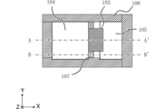
図1は、実施形態1に係る画素の断面的な構成例を示す図である。図2は、光の入射方向から見た実施形態1に係る画素の平面的な構成例を示す図である。なお、図1は、図2におけるAA’間の断面図を示している。 FIG. 1 is a diagram showing an example of a cross-sectional configuration of a pixel according to the first embodiment. FIG. 2 is a diagram illustrating a planar configuration example of a pixel according to the first embodiment as viewed from the direction of light incidence. Note that FIG. 1 shows a cross-sectional view along line AA' in FIG.
図1のように、画素11は、図1の下側から順に、配線層51、酸化膜52、半導体基板53、誘電材料層54、カラーフィルタ層55、およびオンチップレンズ109が積層されて構成されている。図1は、1つの画素11を示しているが、複数の画素11が図1に示された構造を有していてもよい。また、半導体基板53に光電変換部104が形成されている領域を光電変換部領域56と称し、半導体基板53に電荷保持部105が形成されている領域を電荷保持部領域57と称する。画素11は、また、浮遊拡散領域(以下、FD)、FDに蓄積されている電荷に応じた信号を出力する増幅トランジスタ(いずれも不図示)を有する。なお、一般に半導体基板53は2つの表面を持つ。本実施形態では、便宜的に、図1における上側の表面が第1面である。一方、図1における下側の表面が第2面である。図1が示す通り、半導体基板53の第2面の側には配線層51が配される。一方、半導体基板53には、第1面の側から光が入射する。すなわち、本実施形態の光電変換装置は、半導体基板53の配線層が配される側の表面とは反対の表面から入射光が照射される、いわゆる裏面照射型CMOSイメージセンサである。
As shown in FIG. 1, the
光電変換部104は、オンチップレンズ109を介して受光した光を電荷に変換する。電荷保持部105は、光電変換部104から転送された電荷を一時的に保持する。転送ゲート103に供給される電圧によって、光電変換部104から電荷保持部への電荷の転送が制御される。本実施形態では、電荷保持部105は電子を信号電荷として保持する。そのため、光電変換部104および電荷保持部105は、それぞれ、半導体基板53に配されたN型の半導体領域を含んで構成される。N型は、信号電荷と同じ極性である、電子を多数キャリアとする半導体領域の導電型である。ホールを信号電荷として扱う場合には、光電変換部104および電荷保持部105は、それぞれ、半導体基板53に配されたP型の半導体領域を含んで構成される。
The
配線層51は、複数層の配線101を含み、光電変換部104の受光面と反対側に形成される。光電変換部104の受光面は、半導体基板53の第1面の一部である。配線層51は、複数の配線101が層間絶縁膜102に埋めこまれて構成されている。複数の配線101は、光電変換部104の電荷の読み出しに用いられる制御信号や光電変換部104
の電荷に基づく信号を、伝達したり保持したりする。
The
transmits and holds signals based on the electric charge of
配線層51の下側に、基板支持材(不図示)が配置されもよい。例えば、配線層51および半導体基板53に形成されたトランジスタなどの素子(不図示)が、電荷の読み出し回路を構成し、読み出し後のAD変換回路およびその後段の回路が基板支持材に形成されうる。すなわち、本実施形態の光電変換装置は、いわゆる積層型のイメージセンサであってもよい。このような構成により、イメージセンサを高速に駆動させることや高機能化を実現することができる。
A substrate support material (not shown) may be placed below the
また、配線層51のうち、光電変換部104および電荷保持部105の間の領域に、半導体基板53に対して酸化膜52を介して、転送ゲート103が配置されている。転送ゲート103は、半導体基板53の第2面の側に配されている。転送ゲート103に所定の電圧が印加されることにより、光電変換部104に蓄積されている電荷が電荷保持部105に転送される。酸化膜52は、絶縁性を備えており、転送ゲート103のゲート絶縁膜を構成する。すなわち、光電変換部104のN型半導体領域、転送ゲート103、および、電荷保持部105のN型半導体領域は、MOSトランジスタを構成する。
Further, in the
誘電材料層54には、遮光膜108と遮光部106と遮光部107とが、埋め込まれて形成されている。遮光膜108、遮光部106、および遮光部107はいずれも、遮光性を有する材料により形成されている。
A
遮光膜108は、半導体基板53の受光面側(図の上側)に形成され、電荷保持部105への光の入射を遮蔽する。遮光膜108は、少なくとも電荷保持部105の一部を覆うように形成され、好ましくは、電荷保持部105の全部を覆うように形成される。遮光膜108が電荷保持部105を覆うとは、平面視において遮光膜108の領域の中に電荷保持部105の領域が含まれることを意味する。さらに好ましくは、遮光膜108は、光電変換部104の領域を除く全ての領域を覆うように形成される。これにより、電荷保持部への入射光をより低減することができる。また、遮光膜108は、タングステンやアルミ、銅等の材料で形成することで、電荷保持部105への入射光の侵入をより効果的に防ぐことができる。なお、遮光膜108が省略され、第2面側からの平面視において電荷保持部105が露出していてもよい。電荷保持部105が露出していても、遮光部106によって、より良好な画素信号を得るという効果を得ることができる。
The light-shielding
遮光部106および遮光部107は、光電変換部104および電荷保持部105の周囲を囲い、遮光膜108と直交する方向(遮光膜108の法線方向)に延在するように、所定の深さまで形成されている。また、半導体基板53には、遮光部106および遮光部107を配置するための溝が設けられている。遮光部106および遮光部107が導電性材料で構成される場合、溝には、遮光部106または遮光部107に加えて、当該遮光部106または遮光部107と半導体基板53とを絶縁するための絶縁材料が埋め込まれていてもよい。なお、光電変換部104と電荷保持部105の間に形成されている遮光部を遮光部107と称し、それ以外を遮光部106と称する。なお、遮光部107と遮光部106とを区別して説明している場合を除き、遮光部107および遮光部106の一方についての説明は、他方にも適用される。
The
半導体基板53に設けられた溝の内部に遮光部107を形成する場合、当該溝が半導体基板53の第2面(転送ゲート103の配された面)まで到達していると電荷転送ができなくなる。そのため、少なくとも光電変換部104と電荷保持部105との間で転送チャネルが形成されるべき領域においては、遮光部107の配された溝、ならびに、遮光部107が半導体基板53の第2面から離間している。遮光部107の全ての部分を転送ゲート103あるいは半導体基板53の第2面から離して設けてもよい。また、同様に、遮光
部106を半導体基板53の第2面から離して設けていてもよい。このように、遮光部106および遮光部107の全部が同程度の深さまで形成される構成は、製造工程の増加を招くことがない点で有利である。
When forming the
しかし遮光部107が半導体基板53の第2面から離れて設けられる場合、遮光部107と半導体基板53の第2面の間等から、入射光が電荷保持部105に侵入することがある。そこで、電荷保持部105への入射光の侵入を抑制するために、図2,図3に示すように、転送ゲート103直下以外の領域の少なくとも一部において、遮光部107を半導体基板53の第2面まで延在するように設けることが望ましい。この場合、遮光部107の配された溝は、半導体基板53の第1面から第2面まで貫通する。本構成により、斜め入射光が電荷保持部105に侵入することを低減することができる。
However, when the
図1の例では、遮光部106を半導体基板53の第2面から離して設けているが、遮光部106も同様に、半導体基板53の第2面に接するように設けてもよい。このような構成により、隣接画素に入射した光のクロストーク等による光学的なノイズを低減することができる。
In the example of FIG. 1, the
遮光部107の一部および遮光部106を半導体基板53の表面に接するように配置した構成例を図3に示す。図3は図2におけるBB’間の断面図である。
FIG. 3 shows a configuration example in which a part of the
また、遮光部106と遮光部107と遮光膜108には、任意の電圧が供給されてもよい。例えば、遮光部106と遮光部107と遮光膜108は、接地電位(GND)に固定される。遮光部106の電位が変化すると、遮光部106等に対して寄生のカップリング容量を持つ他のノードの電位も変化する、つまり、クロストークが生じる可能性がある。遮光部106等の電位変化は、遮光部106等の電位が制御されている場合、制御回路によって生じうる。また、遮光部106等の電位変化は、遮光部106等がフローティングの場合、他のノードの電位変動によって生じることもある。これに対して、遮光部106等の電位を固定することにより、遮光部106と遮光部107と遮光膜108の電位変化に起因するクロストーク等の影響を低減することができる。
Moreover, arbitrary voltages may be supplied to the
図4に、遮光部106と遮光部107と遮光膜108に電圧を供給する方法の一例を示す。図4の例では、配線101と遮光部106とが、コンタクト部110を介して直接接続されている。別の例では、誘電材料層54側で遮光膜108と配線とを接続して、遮光膜108に電圧を供給することもできる。ただしこの場合、誘電材料層54側に追加で配線を配置する必要があり、画素レイアウトが制限され、開口率が小さくなり、画素性能が低下する可能性がある。更に別の例では、半導体基板53の第2面付近に高濃度の拡散層を設け、当該拡散層を介してコンタクト部110と遮光部106とを電気的に接続することもできる。本構成においては、深い遮光部106を形成する必要がなく、製造が容易となる。
FIG. 4 shows an example of a method of supplying voltage to the
なお、電位固定は、画素ごとに実施することが望ましい。画素ごとの電位固定により、遮光部106と遮光部107と遮光膜108の画素間の電位変動が小さくなり、配線101との容量カップリングによるクロストーク等の影響をより低減させることができる。また、本構成は、配線層51下に基板支持材を配置する積層構成にすることが望ましい。これにより、誘電材料層54側に追加で配線を配置する必要がなく、画素レイアウトの自由度が向上し、開口率を大きくすることができる。
Note that potential fixing is preferably performed for each pixel. By fixing the potential for each pixel, potential fluctuations between the pixels of the
本実施形態において、遮光部106および遮光部107は、遮光膜108と同様に、タングステンやアルミ、銅等の材料により形成する。それにより、隣接画素に入射した光のクロストークや、電荷保持部105への入射光の侵入を効果的に防ぎ、光学的なノイズを
低減することができる。
In this embodiment, the
本実施形態において、光電変換部104と電荷保持部105との間に配置される遮光部107は、電荷保持部105より光電変換部104に近い位置に配置されている。換言すると、遮光部107と光電変換部104との距離は、遮光部107と電荷保持部105との距離より短い。より具体的には、遮光部107と光電変換部104のN型半導体領域との距離が、遮光部107と電荷保持部105のN型半導体領域との距離より短い。遮光部107の少なくとも一部がこの条件を満たす限り、遮光部107、遮光部106、および、遮光膜108の配置は特定の形態に限定されない。上述したように、遮光部106および遮光膜108は配置されていなくてもよい。以下、遮光部107の配置について、図5A~5Cを参照して説明する。図5A~図5Cは、光電変換部104、電荷保持部105、遮光部107のみを示した平面図である。
In this embodiment, the
図5Aは、図1,図2に示した例と同一の構成であり、遮光部107の全ての部分が、光電変換部104と電荷保持部105の隣接方向(X方向)に関して、光電変換部104と電荷保持部105の中間よりも光電変換部104に近い領域内に配置されている。
5A has the same configuration as the example shown in FIGS. 1 and 2, and all parts of the
しかしながら、図5Bに示すように、遮光部107のX方向についての中心が、光電変換部104と電荷保持部105の中間よりも光電変換部104側に位置していればよい。言い換えると、遮光部107の一部が光電変換部104と電荷保持部105の中間よりも電荷保持部105に近い領域に位置してもよい。
However, as shown in FIG. 5B, the center of the
また、図5A,図5Bに示す例では、Y方向の全ての位置において、光電変換部104から遮光部107までのX方向に沿った距離が、電荷保持部105から遮光部107までのX方向に沿った距離よりも小さい。しかし、これは必須ではない。図5Cに示すように、遮光部107のY方向位置の少なくとも一部において、光電変換部104から遮光部107までのX方向に沿った距離が、電荷保持部105から遮光部107までのX方向に沿った距離よりも小さいという構成としてもよい。このような構成でも、入射光の侵入を防止する効果が得られる。なお、画素の中心に光が多く入射することから、遮光部107のY方向中央部分107aは、電荷保持部105よりも光電変換部104に近い位置に配置されることが好ましい。遮光部107の周辺部分107b,107cは、光電変換部104と電荷保持部105の中間に配置されてもよいし、電荷保持部105に近い領域に配置されてもよい。また、転送ゲート103と重なる位置では、遮光部107は電荷保持部105よりも光電変換部104に近い位置に配置されることが好ましい。
Furthermore, in the examples shown in FIGS. 5A and 5B, at all positions in the Y direction, the distance along the X direction from the
本実施形態によれば、入射光が電荷保持部105へ侵入することを効果的に防止できる。画素に対して斜め方向から光が入射した場合、入射光は、オンチップレンズ109により集光され、カラーフィルタ層55、誘電材料層54、半導体基板53、光電変換部104を透過する。この透過光は、図1の白抜きの矢印で示すように、遮光部107によって遮光される。本実施形態では、遮光部107の少なくとも一部が、光電変換膜104の近くに配置される。結果として、電荷保持部領域57への入射光が減少し、従来に比べさらに光学的なノイズを低減することができる。
According to this embodiment, it is possible to effectively prevent incident light from entering the
なお、半導体基板53の光電変換部104に入射した光を少なくとも部分的に遮光することができれば、本実施形態の効果は得られる。他の経路から電荷保持部105に入射する光が多少にかかわらず存在することは、本実施形態の解決すべき課題とは関係がない。例えば、電荷保持部105が、特定の方向からの光に対して遮蔽され、他の方向からの光を受けるように構成されることが望ましい場合がある。
Note that the effects of this embodiment can be obtained as long as the light incident on the
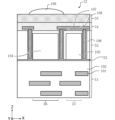
[実施形態2]
図6は、実施形態2に係る画素の断面的な構成例を示す図である。図7は、光の入射方向から見た実施形態2に係る画素の平面的な構成例を示す図である。図6は、図7におけるCC’間の断面図を示している。図1~図5と同じ機能を有する部分には、同じ符号を付している。図1~図5の同様の要素についての説明は、適宜、図6および図7に援用される。
[Embodiment 2]
FIG. 6 is a diagram illustrating a cross-sectional configuration example of a pixel according to the second embodiment. FIG. 7 is a diagram illustrating a planar configuration example of a pixel according to the second embodiment as viewed from the light incident direction. FIG. 6 shows a cross-sectional view between CC' in FIG. Components having the same functions as those in FIGS. 1 to 5 are given the same reference numerals. Descriptions of similar elements in FIGS. 1-5 are incorporated into FIGS. 6 and 7, as appropriate.
図6のように、画素14は、図6の下側から順に、配線層51、酸化膜52、半導体基板53、誘電材料層54、カラーフィルタ層55、およびオンチップレンズ109が積層されて構成されている。図6は、1つの画素14を示しているが、複数の画素14が図6に示された構造を有していてもよい。また、半導体基板53に光電変換部104が形成されている領域を光電変換部領域56と称し、半導体基板53に電荷保持部105が形成されている領域を電荷保持部領域57と称する。本実施形態の光電変換装置は、半導体基板53の配線層が配される側の表面とは反対の面から入射光が照射される、いわゆる裏面照射型CMOSイメージセンサである。
As shown in FIG. 6, the
配線層51は、複数層の配線101を含み、光電変換部104の受光面と反対側に形成される。光電変換部104の受光面は、半導体基板53の第1面の一部である。配線層51は、複数の配線101が層間絶縁膜102に埋めこまれて構成されている。複数の配線101は、光電変換部104の電荷の読み出しに用いられる制御信号や光電変換部104の電荷に基づく信号を、伝達したり保持したりする。
The
また、配線層51のうち、光電変換部104および電荷保持部105の間の領域に、半導体基板53に対して酸化膜52を介して、転送ゲート103が配置されている。転送ゲート103は、半導体基板53の第2面の側に配されている。転送ゲート103に所定の電圧が印加されることにより、光電変換部104に蓄積されている電荷が電荷保持部105に転送される。酸化膜52は、絶縁性を備えており、転送ゲート103のゲート絶縁膜を構成する。すなわち、光電変換部104のN型半導体領域、転送ゲート103、および、電荷保持部105のN型半導体領域は、MOSトランジスタを構成する。
Further, in the
誘電材料層54には、遮光性を有する材料により形成されている遮光膜108と遮光部106と遮光部107とが、埋め込まれて形成されている。遮光膜108、遮光部106、および遮光部107はいずれも、遮光性を有する材料により形成されている。
A light-shielding
遮光膜108は、少なくとも電荷保持部105を覆うように形成されている。遮光部106および遮光部107は、光電変換部104および電荷保持部105の周囲を囲い、遮光膜108と直交する方向(遮光膜108の法線方向)に延在するように、所定の深さまで形成されている。また、半導体基板53には、遮光部106および遮光部107を配置するための溝が設けられている。遮光部106および遮光部107が導電性材料で構成される場合、溝には、遮光部106または遮光部107に加えて、当該遮光部106または遮光部107と半導体基板53とを絶縁するための絶縁材料が埋め込まれていてもよい。なお、光電変換部104と電荷保持部105の間に形成されている遮光部を遮光部107と称し、それ以外を遮光部106と称する。なお、遮光部107と遮光部106とを区別して説明している場合を除き、遮光部107および遮光部106の一方についての説明は、他方にも適用される。
The
半導体基板53に設けられた溝の内部に遮光部107を形成する場合、当該溝が半導体基板53の第2面(転送ゲート103の配された面)まで到達していると電荷転送ができなくなる。そのため、少なくとも光電変換部104と電荷保持部105との間で転送チャネルが形成されるべき領域においては、遮光部107の配された溝、ならびに、遮光部107が半導体基板53の第2面から離間している。遮光部107の全ての部分を転送ゲー
ト103あるいは半導体基板53の第2面から離して設けてもよい。また、同様に、遮光部106を半導体基板53の第2面から離して設けていてもよい。このように、遮光部106および遮光部107の全部が同程度の深さまで形成される構成は、製造工程の増加を招くことがない点で有利である。
When forming the
しかし遮光部107が半導体基板53の第2面から離れて設けられる場合、遮光部107と半導体基板53の表面の間等から、入射光が電荷保持部105に侵入することがある。そこで、電荷保持部105への入射光の侵入を抑制するために、図2に示すように、転送ゲート103直下以外の領域の少なくとも一部において、遮光部107を半導体基板53の表面まで延在するように設けることが望ましい。この場合、遮光部107の配された溝は、半導体基板53の第1面から第2面まで貫通する。本構成により、斜め入射光が電荷保持部105に侵入することを低減することができる。
However, when the
図6の例では、遮光部106を半導体基板53から離して設けているが、遮光部106においても同様に、半導体基板53の表面に接するよう設けてもよい。このような構成により、隣接画素に入射した光のクロストーク等による光学的なノイズを低減することができる。
In the example of FIG. 6, the
また、遮光部106と遮光部107と遮光膜108には、任意の電圧が供給されてもよい。例えば、遮光部106と遮光部107と遮光膜108は、接地電位(GND)に固定される。遮光部106の電位が変化すると、遮光部106等に対して寄生のカップリング容量を持つ他のノードの電位も変化する、つまり、クロストークが生じる可能性がある。遮光部106等の電位変化は、遮光部106等の電位が制御されている場合、制御回路によって生じうる。また、遮光部106等の電位変化は、遮光部106等がフローティングの場合、他のノードの電位変動によって生じることもある。これに対して、遮光部106等の電位を固定することにより、遮光部106と遮光部107と遮光膜108の電位変化に起因するクロストーク等の影響を低減することができる。電位固定方法については、実施形態1に記載しているため、省略する。
Moreover, arbitrary voltages may be supplied to the
遮光部106および遮光部107は、遮光膜108と同様に、タングステンやアルミ、銅等の材料により形成する。それにより、隣接画素に入射した光のクロストークや、電荷保持部105への入射光の侵入を効果的に防ぎ、光学的なノイズを低減することができる。
The
また、光電変換部104と電荷保持部105との間に配置される遮光部107は、電荷保持部105より前記光電変換部に近い位置に配置されている。遮光部107の配置の詳細については、実施形態1に記載しているため、省略する。
Further, the
実施形態1で説明したように、光電変換部104への斜め入射光が、電荷保持部105に侵入する可能性がある。この経路以外に、半導体基板53を透過した光が配線層51で反射し、その反射光が電荷保持部105に侵入することがある。具体的には、画素14への斜め方向からの光が光電変換部104、酸化膜52を透過して、配線層51に入射することがある。そして、特に光電変換部領域56に配置される配線101において入射光が反射すると、転送ゲート103と遮光部107あるいは半導体基板53の表面との間から、その反射光が電荷保持部105に侵入することがある。
As described in the first embodiment, obliquely incident light on the
実施形態2では、転送ゲート103と、配線層内の層間絶縁膜102に埋め込まれている複数の配線101のうち転送ゲート103に最も近い配線との間に、遮光膜111が配置されている。図6では、転送ゲート103と最上層の配線101の間に遮光膜111が配置されている。本構成により、光電変換部104を透過し、層間絶縁膜102に埋め込
まれている配線101で反射した光を、遮光膜111で遮り、電荷保持部領域57に入射することを防止することができる。遮光膜111が設けられていない構成では、配線101で反射した光が電荷保持部105に入射し、光学的なノイズが発生することが想定される。本実施形態では、このようなノイズの発生を防止できる。
In the second embodiment, a
さらに、遮光膜111は、配線101で反射した光が、図6の点線で示している通り、光電変換部104に近い側の遮光部107の下端に到達する反射光線を遮る位置に形成されることが望ましい。本構成により、配線101からの反射光をより効果的に遮ることができる。
Further, the
また、遮光膜111は、遮光膜111が少なくとも電荷保持部領域57を覆うように広く配置することができる。遮光膜111が電荷保持部領域57を覆うとは、平面視において遮光膜111の領域の中に電荷保持部領域57すなわち電荷保持部105の領域が含まれることを意味する。遮光膜111を広く配置することにより、配線層51に配置されている複数の配線101からの反射光を遮ることができる。
Further, the
一方、光電変換部領域56に配置する遮光膜111は、電荷保持部105への反射光を発生させる要因となったり、配線101と遮光膜111との間の寄生容量が大きくなる原因となったりすることもある。よって、なるべく遮光膜111の配置領域を小さくすることが望ましい。このために、遮光膜111と遮光部107とを次のような構成とするとよい。遮光部107は、実施形態1の図3に示したように、転送ゲート103直下を除き、半導体基板53の表面に接するように設ける。遮光膜111は、光電変換部104の一部を覆い、かつ、転送ゲート103を覆うように配置する。転送ゲート103を覆うので、遮光膜111の幅はゲート幅Wと等しい。遮光部107と転送ゲート103の間に隙間があると、転送ゲート103の直下すなわち、遮光部107と転送ゲート103の間が反射光の侵入経路となり得る。そこで、遮光膜111を上記のように設けることで、電荷保持部105への反射光の侵入を防止できる。さらに、遮光膜111の幅をゲート幅Wより大きくし、転送ゲート103が配置されておらず、かつ、遮光部107が半導体基板53の表面に接していない領域の下部にも遮光膜111が配置することでさらに高い効果が得られる。
On the other hand, the light-shielding
本構成では、遮光膜111からの反射光の侵入を限りなく小さくし、導電性材料の遮光膜111による寄生容量を低下させることができる。
With this configuration, the penetration of reflected light from the
また、上記の例では、遮光膜111の幅が転送ゲート103のゲート幅以上であり転送ゲート103を覆う構成であるが、遮光膜111は転送ゲート103の少なくとも一部を覆うように形成されればよい。したがって、遮光膜111は、光電変換部104の一部を覆い、かつ転送ゲート103のゲート幅未満とすることもできる。本構成では、配線101からの反射光の侵入を少なくとも部分的に遮ることができ、かつ、導電性材料の遮光膜111による寄生容量を最小限にすることができる。
Further, in the above example, the width of the
なお、図6には図示していないが、遮光膜111と配線101との容量カップリングによるクロストーク等の影響を避けるため、任意の固定電位、例えばGNDに設定されている。
Although not shown in FIG. 6, in order to avoid effects such as crosstalk due to capacitive coupling between the
本実施形態によれば、入射光が電荷保持部105へ侵入することをさらに効果的に防止できる。画素に対して斜め方向から光が入射した場合、入射光は、オンチップレンズ109により集光され、カラーフィルタ層55、誘電材料層54、半導体基板53、光電変換部104、酸化膜52を透過する。この透過光が光電変換部領域56の配線101によって反射しても、遮光膜111によって効果的に遮光することができる。結果として、電荷
保持部領域57への入射光が減少し、光学的なノイズを低減することができる。
According to this embodiment, it is possible to more effectively prevent incident light from entering the
[実施形態3]
本発明の実施形態3による撮像システムについて、図8を用いて説明する。図8は、本実施形態による撮像システムの概略構成を示すブロック図である。
[Embodiment 3]
An imaging system according to Embodiment 3 of the present invention will be described using FIG. 8. FIG. 8 is a block diagram showing a schematic configuration of an imaging system according to this embodiment.
上記実施形態1,2で述べた固体撮像装置(光電変換装置)は、種々の撮像システムに適用可能である。適用可能な撮像システムとしては、特に限定されるものではないが、例えば、デジタルスチルカメラ、デジタルカムコーダ、監視カメラ、複写機、ファックス、携帯電話、車載カメラ、観測衛星、医療用カメラなどの各種の機器が挙げられる。また、レンズなどの光学系と固体撮像装置(光電変換装置)とを備えるカメラモジュールも、撮像システムに含まれる。図8にはこれらのうちの一例として、デジタルスチルカメラのブロック図を例示している。 The solid-state imaging device (photoelectric conversion device) described in Embodiments 1 and 2 above can be applied to various imaging systems. Applicable imaging systems include, but are not limited to, various types such as digital still cameras, digital camcorders, surveillance cameras, copiers, faxes, mobile phones, vehicle cameras, observation satellites, and medical cameras. Examples include equipment. Further, a camera module including an optical system such as a lens and a solid-state imaging device (photoelectric conversion device) is also included in the imaging system. FIG. 8 shows a block diagram of a digital still camera as an example of these.
撮像システム2000は、図8に示すように、撮像装置100、撮像光学系2002、CPU2010、レンズ制御部2012、撮像装置制御部2014、画像処理部2016、絞りシャッター制御部2018を備える。撮像システム2000は、また、表示部2020、操作スイッチ2022、記録媒体2024を備える。
As shown in FIG. 8, the
撮像光学系2002は、被写体の光学像を形成するための光学系であり、レンズ群、絞り2004等を含む。絞り2004は、その開口径を調節することで撮影時の光量調節を行なう機能を備えるほか、静止画撮影時には露光秒時調節用シャッターとしての機能も備える。レンズ群及び絞り2004は、光軸方向に沿って進退可能に保持されており、これらの連動した動作によって変倍機能(ズーム機能)や焦点調節機能を実現する。撮像光学系2002は、撮像システムに一体化されていてもよいし、撮像システムへの装着が可能な撮像レンズでもよい。
The imaging
撮像光学系2002の像空間には、その撮像面が位置するように撮像装置100が配置されている。撮像装置100は、実施形態1,2で説明した固体撮像装置(光電変換装置)であり、CMOSセンサ(画素部)とその周辺回路(周辺回路領域)とを含んで構成される。撮像装置100は、複数の光電変換部を有する画素が2次元配置され、これらの画素に対してカラーフィルタが配置されることで、2次元単板カラーセンサを構成している。撮像装置100は、撮像光学系2002により結像された被写体像を光電変換し、画像信号や焦点検出信号として出力する。
The
レンズ制御部2012は、撮像光学系2002のレンズ群の進退駆動を制御して変倍操作や焦点調節を行うためのものであり、その機能を実現するように構成された回路や処理装置により構成されている。絞りシャッター制御部2018は、絞り2004の開口径を変化して(絞り値を可変として)撮影光量を調節するためのものであり、その機能を実現するように構成された回路や処理装置により構成される。
The
CPU2010は、カメラ本体の種々の制御を司るカメラ内の制御装置であり、演算部、ROM、RAM、A/Dコンバータ、D/Aコンバータ、通信インターフェイス回路等を含む。CPU2010は、ROM等に記憶されたコンピュータプログラムに従ってカメラ内の各部の動作を制御し、撮像光学系2002の焦点状態の検出(焦点検出)を含むAF、撮像、画像処理、記録等の一連の撮影動作を実行する。CPU2010は、信号処理部でもある。
The
撮像装置制御部2014は、撮像装置100の動作を制御するとともに、撮像装置100から出力された信号をA/D変換してCPU2010に送信するためのものであり、そ
れら機能を実現するように構成された回路や制御装置により構成される。A/D変換機能は、撮像装置100が備えていてもかまわない。画像処理部2016は、A/D変換された信号に対してγ変換やカラー補間等の画像処理を行って画像信号を生成する処理装置であり、その機能を実現するように構成された回路や制御装置により構成される。表示部2020は、液晶表示装置(LCD)等の表示装置であり、カメラの撮影モードに関する情報、撮影前のプレビュー画像、撮影後の確認用画像、焦点検出時の合焦状態等を表示する。操作スイッチ2022は、電源スイッチ、レリーズ(撮影トリガ)スイッチ、ズーム操作スイッチ、撮影モード選択スイッチ等で構成される。記録媒体2024は、撮影済み画像等を記録するためのものであり、撮像システムに内蔵されたものでもよいし、メモリカード等の着脱可能なものでもよい。
The imaging
このようにして、実施形態1,2による撮像装置100を適用した撮像システム2000を構成することにより、高性能の撮像システムを実現することができる。
In this way, by configuring the
[実施形態4]
本発明の実施形態4による撮像システム及び移動体について、図9A及び図9Bを用いて説明する。図9A及び図9Bは、本実施形態による撮像システム及び移動体の構成を示す図である。
[Embodiment 4]
An imaging system and a moving object according to Embodiment 4 of the present invention will be described using FIGS. 9A and 9B. 9A and 9B are diagrams showing the configurations of an imaging system and a moving object according to this embodiment.
図9Aは、車載カメラに関する撮像システム2100の一例を示したものである。撮像システム2100は、撮像装置2110を有する。撮像装置2110は、上述の実施形態1,2に記載の固体撮像装置(光電変換装置)のいずれかである。撮像システム2100は、画像処理部2112と視差取得部2114を有する。画像処理部2112は、撮像装置2110により取得された複数の画像データに対し、画像処理を行う処理装置である。視差取得部2114は、撮像装置2110により取得された複数の画像データから視差(視差画像の位相差)の算出を行う処理装置である。また、撮像システム2100は、算出された視差に基づいて対象物までの距離を算出する処理装置である距離取得部2116と、算出された距離に基づいて衝突可能性があるか否かを判定する処理装置である衝突判定部2118と、を有する。ここで、視差取得部2114や距離取得部2116は、対象物までの距離情報等の情報を取得する情報取得手段の一例である。すなわち、距離情報とは、視差、デフォーカス量、対象物までの距離等に関する情報である。衝突判定部2118はこれらの距離情報のいずれかを用いて、衝突可能性を判定してもよい。上述の処理装置は、専用に設計されたハードウェアによって実現されてもよいし、ソフトウェアモジュールに基づいて演算を行う汎用のハードウェアによって実現されてもよい。また、処理装置はFPGA(Field Programmable Gate Array)、ASIC(Application Specific Integrated Circuit)等によって実現されてもよいし、これらの組合せによって実現されてもよい。
FIG. 9A shows an example of an
撮像システム2100は、車両情報取得装置2120と接続されており、車速、ヨーレート、舵角などの車両情報を取得することができる。また、撮像システム2100は、衝突判定部2118での判定結果に基づいて、車両に対して制動力を発生させる制御信号を出力する制御装置である制御ECU2130が接続されている。すなわち、制御ECU2130は、距離情報に基づいて移動体を制御する移動体制御手段の一例である。また、撮像システム2100は、衝突判定部2118での判定結果に基づいて、ドライバーへ警報を発する警報装置2140とも接続されている。例えば、衝突判定部2118の判定結果として衝突可能性が高い場合、制御ECU2130はブレーキをかける、アクセルを戻す、エンジン出力を抑制するなどして衝突を回避、被害を軽減する車両制御を行う。警報装置2140は音等の警報を鳴らす、カーナビゲーションシステムなどの画面に警報情報を表示する、シートベルトやステアリングに振動を与えるなどしてユーザに警告を行う。
The
本実施形態では、車両の周囲、例えば前方又は後方を撮像システム2100で撮像する。図9Bに、車両前方(撮像範囲2150)を撮像する場合の撮像システム2100を示した。車両情報取得装置2120は、撮像システム2100を動作させ撮像を実行させるように指示を送る。上述の実施形態1,2の撮像装置を撮像装置2110として用いることにより、本実施形態の撮像システム2100は、測距の精度をより向上させることができる。
In this embodiment, the
以上の説明では、他の車両と衝突しないように制御する例を述べたが、他の車両に追従して自動運転する制御、車線からはみ出さないように自動運転する制御等にも適用可能である。更に、撮像システムは、自動車等の車両に限らず、例えば、船舶、航空機あるいは産業用ロボットなどの移動体(輸送機器)に適用することができる。移動体(輸送機器)における移動装置はエンジン、モーター、車輪、プロペラなどの各種の駆動源である。加えて、移動体に限らず、高度道路交通システム(ITS)等、広く物体認識を利用する機器に適用することができる。 In the above explanation, we have described an example of control to avoid collisions with other vehicles, but it can also be applied to control to automatically drive while following other vehicles, control to automatically drive to avoid moving out of the lane, etc. be. Furthermore, the imaging system can be applied not only to vehicles such as automobiles, but also to moving objects (transportation equipment) such as ships, aircraft, and industrial robots. Mobility devices in moving bodies (transportation equipment) include various drive sources such as engines, motors, wheels, and propellers. In addition, the present invention can be applied not only to mobile objects but also to a wide range of devices that use object recognition, such as intelligent transportation systems (ITS).
51 配線層
103 転送ゲート
104 光電変換部
105 電荷保持部
107 遮光部
51
Claims (19)
前記半導体基板に配された浮遊拡散領域と、
前記半導体基板に配され、入射した光を電荷に変換する光電変換部と、
前記半導体基板に配され、前記光電変換部から転送された電荷を保持する電荷保持部と、
前記半導体基板のうち前記光電変換部と前記電荷保持部の間に設けられた溝に配された遮光部と、
前記半導体基板の前記第2面の側に形成され、前記光電変換部の電荷を前記電荷保持部に転送する転送ゲートと、
を有し、
平面視において前記遮光部と前記転送ゲートとが重なり、
前記遮光部と前記光電変換部との距離は、前記遮光部と前記電荷保持部との距離より短い、
ことを特徴とする光電変換装置。 a semiconductor substrate having a first surface onto which light enters and a second surface opposite to the first surface;
a floating diffusion region disposed on the semiconductor substrate;
a photoelectric conversion unit disposed on the semiconductor substrate and converting incident light into charges;
a charge holding section disposed on the semiconductor substrate and holding charges transferred from the photoelectric conversion section;
a light shielding part disposed in a groove provided between the photoelectric conversion part and the charge holding part in the semiconductor substrate;
a transfer gate that is formed on the second surface side of the semiconductor substrate and that transfers the charge of the photoelectric conversion section to the charge holding section;
has
The light shielding portion and the transfer gate overlap in plan view,
The distance between the light shielding part and the photoelectric conversion part is shorter than the distance between the light shielding part and the charge holding part.
A photoelectric conversion device characterized by:
前記電荷保持部は、前記第1導電型の第2半導体領域を含み、
前記遮光部と前記光電変換部の前記第1半導体領域との距離が、前記遮光部と前記電荷保持部の前記第2半導体領域との距離より短い、
請求項1に記載の光電変換装置。 The photoelectric conversion section includes a first semiconductor region of a first conductivity type whose majority carriers are charges having the same polarity as the charges held by the charge holding section,
The charge holding section includes the second semiconductor region of the first conductivity type,
The distance between the light shielding part and the first semiconductor region of the photoelectric conversion part is shorter than the distance between the light shielding part and the second semiconductor region of the charge holding part.
The photoelectric conversion device according to claim 1.
請求項1または2に記載の光電変換装置。 The groove provided in the semiconductor substrate is spaced apart from the second surface in at least a portion of a region overlapping with the transfer gate when viewed in plan with respect to the first surface or the second surface.
The photoelectric conversion device according to claim 1 or 2.
前記半導体基板は、入射した光を電荷に変換する光電変換部が配される第1半導体領域と、前記光電変換部から転送された電荷を保持する電荷保持部が配される第2半導体領域と、を含み、
前記第1半導体領域と前記第2半導体領域とを通る断面において、前記遮光部は前記光電変換部と前記電荷保持部の間に配され、
前記半導体基板の前記第2面の側に形成され、前記光電変換部の電荷を前記電荷保持部に転送する転送ゲートを有し、
平面視において前記遮光部と前記転送ゲートとが重なり、
前記遮光部と前記光電変換部との距離は、前記遮光部と前記電荷保持部との距離より短い、
ことを特徴とする光電変換装置。 A photoelectric conversion device comprising a semiconductor substrate having a first surface onto which light enters and a second surface opposite to the first surface, and a light shielding part,
The semiconductor substrate includes a first semiconductor region in which a photoelectric conversion section that converts incident light into charges is disposed, and a second semiconductor region in which a charge holding section that retains charges transferred from the photoelectric conversion section is disposed. , including;
In a cross section passing through the first semiconductor region and the second semiconductor region, the light shielding section is arranged between the photoelectric conversion section and the charge holding section,
a transfer gate formed on the second surface side of the semiconductor substrate to transfer the charge of the photoelectric conversion section to the charge holding section;
The light shielding portion and the transfer gate overlap in plan view,
The distance between the light shielding part and the photoelectric conversion part is shorter than the distance between the light shielding part and the charge holding part.
A photoelectric conversion device characterized by:
請求項1から4のいずれか1項に記載の光電変換装置。 The light shielding section is arranged in a region closer to the photoelectric conversion section than between the photoelectric conversion section and the charge holding section,
The photoelectric conversion device according to any one of claims 1 to 4.
前記遮光部は、前記転送ゲートの直下以外の領域の少なくとも一部において、前記半導体基板の前記第2面まで延在する、
請求項1から5のいずれか1項に記載の光電変換装置。 The light shielding portion includes a portion disposed in a region other than directly under the transfer gate,
The light shielding portion extends to the second surface of the semiconductor substrate in at least a portion of a region other than directly below the transfer gate.
The photoelectric conversion device according to any one of claims 1 to 5.
前記遮光部の配された前記溝は、転送ゲートの直下以外の領域の少なくとも一部において、前記半導体基板の前記第1面から前記第2面まで貫通する、
請求項1から3のいずれか1項に記載の光電変換装置。 The light shielding portion includes a portion disposed in a region other than directly under the transfer gate,
The groove in which the light shielding portion is arranged penetrates from the first surface to the second surface of the semiconductor substrate in at least a portion of a region other than directly under the transfer gate.
The photoelectric conversion device according to any one of claims 1 to 3.
請求項1から7のいずれか1項に記載の光電変換装置。 A first light-shielding film is disposed on the first surface side of the semiconductor substrate so as to cover at least a portion of the charge holding portion.
The photoelectric conversion device according to any one of claims 1 to 7.
請求項8に記載の光電変換装置。 The first light shielding film is arranged to cover all areas except the photoelectric conversion section,
The photoelectric conversion device according to claim 8.
請求項8または9に記載の光電変換装置。 The light shielding part and the first light shielding film are formed of a conductive material, and a voltage is supplied to at least one of the light shielding part and the first light shielding film.
The photoelectric conversion device according to claim 8 or 9.
前記転送ゲートと前記配線層内の配線との間に、第2の遮光膜が配置される、
請求項1から8のいずれか1項に記載の光電変換装置。 further comprising a wiring layer formed on the second surface side of the semiconductor substrate,
a second light shielding film is disposed between the transfer gate and the wiring in the wiring layer;
The photoelectric conversion device according to any one of claims 1 to 8.
請求項11に記載の光電変換装置。 The second light-shielding film is disposed between the transfer gate and a wiring disposed closest to the transfer gate in the wiring layer.
The photoelectric conversion device according to claim 11.
請求項11または12に記載の光電変換装置。 The second light shielding film is formed at a position where light transmitted through the photoelectric conversion section and reflected by the wiring layer blocks reflected light rays that reach a lower end of the light shielding section on the side closer to the photoelectric conversion section.
The photoelectric conversion device according to claim 11 or 12.
請求項11から13のいずれか1項に記載の光電変換装置。 The width of the second light shielding film is greater than or equal to the gate width of the transfer gate.
The photoelectric conversion device according to any one of claims 11 to 13.
請求項11から14のいずれか1項に記載の光電変換装置。 the second light-shielding film covers the charge retention section;
The photoelectric conversion device according to any one of claims 11 to 14.
請求項11から15のいずれか1項に記載の光電変換装置。 In a plan view of the first surface or the second surface, the second light shielding film at least partially overlaps the transfer gate;
The photoelectric conversion device according to any one of claims 11 to 15.
請求項11から16のいずれか1項に記載の光電変換装置。 The second light shielding film is made of a conductive material and is supplied with a voltage.
The photoelectric conversion device according to any one of claims 11 to 16.
前記光電変換装置から出力される信号を処理する信号処理部と、
を有することを特徴とする撮像システム。 A photoelectric conversion device according to any one of claims 1 to 17,
a signal processing unit that processes a signal output from the photoelectric conversion device;
An imaging system comprising:
請求項1から17のいずれか1項に記載の光電変換装置と、
移動装置と、
前記光電変換装置から出力される信号から情報を取得する処理装置と、
前記情報に基づいて前記移動装置を制御する制御装置と、
を有することを特徴とする移動体。 A mobile object,
A photoelectric conversion device according to any one of claims 1 to 17,
a mobile device;
a processing device that acquires information from a signal output from the photoelectric conversion device;
a control device that controls the mobile device based on the information;
A moving body characterized by having.
Priority Applications (2)
| Application Number | Priority Date | Filing Date | Title |
|---|---|---|---|
| JP2019085947A JP7346072B2 (en) | 2019-04-26 | 2019-04-26 | Photoelectric conversion device, imaging system, and mobile object |
| US16/848,953 US11417695B2 (en) | 2019-04-26 | 2020-04-15 | Photoelectric conversion apparatus, imaging system, and moving body |
Applications Claiming Priority (1)
| Application Number | Priority Date | Filing Date | Title |
|---|---|---|---|
| JP2019085947A JP7346072B2 (en) | 2019-04-26 | 2019-04-26 | Photoelectric conversion device, imaging system, and mobile object |
Publications (3)
| Publication Number | Publication Date |
|---|---|
| JP2020181947A JP2020181947A (en) | 2020-11-05 |
| JP2020181947A5 JP2020181947A5 (en) | 2022-04-21 |
| JP7346072B2 true JP7346072B2 (en) | 2023-09-19 |
Family
ID=72921624
Family Applications (1)
| Application Number | Title | Priority Date | Filing Date |
|---|---|---|---|
| JP2019085947A Active JP7346072B2 (en) | 2019-04-26 | 2019-04-26 | Photoelectric conversion device, imaging system, and mobile object |
Country Status (2)
| Country | Link |
|---|---|
| US (1) | US11417695B2 (en) |
| JP (1) | JP7346072B2 (en) |
Families Citing this family (3)
| Publication number | Priority date | Publication date | Assignee | Title |
|---|---|---|---|---|
| KR102607473B1 (en) * | 2017-10-03 | 2023-11-29 | 소니 세미컨덕터 솔루션즈 가부시키가이샤 | Solid-state imaging device, method for manufacturing solid-state imaging device, and electronic device |
| US11463644B2 (en) | 2018-08-31 | 2022-10-04 | Canon Kabushiki Kaisha | Imaging device, imaging system, and drive method of imaging device |
| JP2022094727A (en) * | 2020-12-15 | 2022-06-27 | ソニーセミコンダクタソリューションズ株式会社 | Solid-state imaging device and method for manufacturing the same |
Citations (6)
| Publication number | Priority date | Publication date | Assignee | Title |
|---|---|---|---|---|
| JP2010118412A (en) | 2008-11-11 | 2010-05-27 | Panasonic Corp | Solid-state imaging apparatus, and method of manufacturing the same |
| US20120080732A1 (en) | 2010-10-04 | 2012-04-05 | International Business Machines Corporation | Isolation structures for global shutter imager pixel, methods of manufacture and design structures |
| JP2012169530A (en) | 2011-02-16 | 2012-09-06 | Sony Corp | Solid state image sensor, manufacturing method therefor, and electronic apparatus |
| JP2013065688A (en) | 2011-09-16 | 2013-04-11 | Sony Corp | Solid state imaging element, manufacturing method, and electronic apparatus |
| JP2017168566A (en) | 2016-03-15 | 2017-09-21 | ソニー株式会社 | Solid state imaging device, and electronic apparatus |
| WO2018008614A1 (en) | 2016-07-06 | 2018-01-11 | ソニーセミコンダクタソリューションズ株式会社 | Imaging element, method for producing imaging element, and electronic device |
Family Cites Families (8)
| Publication number | Priority date | Publication date | Assignee | Title |
|---|---|---|---|---|
| JP4315457B2 (en) | 2006-08-31 | 2009-08-19 | キヤノン株式会社 | Photoelectric conversion device and imaging system |
| JP5643555B2 (en) | 2010-07-07 | 2014-12-17 | キヤノン株式会社 | Solid-state imaging device and imaging system |
| JP5656484B2 (en) | 2010-07-07 | 2015-01-21 | キヤノン株式会社 | Solid-state imaging device and imaging system |
| JP2012034350A (en) | 2010-07-07 | 2012-02-16 | Canon Inc | Solid-state imaging device and imaging system |
| JP5697371B2 (en) | 2010-07-07 | 2015-04-08 | キヤノン株式会社 | Solid-state imaging device and imaging system |
| KR102410019B1 (en) * | 2015-01-08 | 2022-06-16 | 삼성전자주식회사 | Image sensor |
| JP6541361B2 (en) | 2015-02-05 | 2019-07-10 | キヤノン株式会社 | Solid-state imaging device |
| US10453885B2 (en) * | 2015-09-09 | 2019-10-22 | Sony Semiconductor Solutions Corporation | Solid-state imaging apparatus and electronic device |
-
2019
- 2019-04-26 JP JP2019085947A patent/JP7346072B2/en active Active
-
2020
- 2020-04-15 US US16/848,953 patent/US11417695B2/en active Active
Patent Citations (6)
| Publication number | Priority date | Publication date | Assignee | Title |
|---|---|---|---|---|
| JP2010118412A (en) | 2008-11-11 | 2010-05-27 | Panasonic Corp | Solid-state imaging apparatus, and method of manufacturing the same |
| US20120080732A1 (en) | 2010-10-04 | 2012-04-05 | International Business Machines Corporation | Isolation structures for global shutter imager pixel, methods of manufacture and design structures |
| JP2012169530A (en) | 2011-02-16 | 2012-09-06 | Sony Corp | Solid state image sensor, manufacturing method therefor, and electronic apparatus |
| JP2013065688A (en) | 2011-09-16 | 2013-04-11 | Sony Corp | Solid state imaging element, manufacturing method, and electronic apparatus |
| JP2017168566A (en) | 2016-03-15 | 2017-09-21 | ソニー株式会社 | Solid state imaging device, and electronic apparatus |
| WO2018008614A1 (en) | 2016-07-06 | 2018-01-11 | ソニーセミコンダクタソリューションズ株式会社 | Imaging element, method for producing imaging element, and electronic device |
Also Published As
| Publication number | Publication date |
|---|---|
| JP2020181947A (en) | 2020-11-05 |
| US20200343287A1 (en) | 2020-10-29 |
| US11417695B2 (en) | 2022-08-16 |
Similar Documents
| Publication | Publication Date | Title |
|---|---|---|
| KR102262794B1 (en) | Solid-state imaging device, imaging system, and movable object | |
| JP6755679B2 (en) | Imaging device | |
| JP7346072B2 (en) | Photoelectric conversion device, imaging system, and mobile object | |
| JP2019133982A (en) | Imaging apparatus, imaging system, and mobile body | |
| JP2017158159A (en) | Imaging apparatus | |
| US10708556B2 (en) | Imaging device and imaging system | |
| EP3890018A1 (en) | Photoelectric conversion apparatus, photoelectric conversion system, and moving object | |
| US10819931B2 (en) | Photoelectric conversion device, imaging system and mobile body | |
| JP7214373B2 (en) | Solid-state imaging device, method for manufacturing solid-state imaging device, and imaging system | |
| US11631712B2 (en) | Photoelectric conversion device, imaging system, and moving body with upper electrode and conductive layer at same potential or connected to each other | |
| US11450701B2 (en) | Photoelectric conversion apparatus, photoelectric conversion system, and movable body | |
| JP7305343B2 (en) | Photoelectric conversion element, method for manufacturing photoelectric conversion element | |
| US11532656B2 (en) | Imaging device and imaging system | |
| JP7346071B2 (en) | Photoelectric conversion device, imaging system, and mobile object | |
| JP7019743B2 (en) | Solid-state image sensor and image sensor | |
| JP7427646B2 (en) | Photoelectric conversion device, photoelectric conversion system, mobile object | |
| JP7342077B2 (en) | Photoelectric conversion device | |
| TWI837162B (en) | Solid-state camera devices and electronic equipment | |
| JP2023174479A (en) | Photoelectric conversion device | |
| JP2023174187A (en) | Photoelectric conversion device, method for manufacturing photoelectric conversion device, imaging system, movable body, and apparatus | |
| JP2022155695A (en) | Photoelectric conversion device, photoelectric conversion system, and mobile body | |
| JP2020170784A (en) | Photoelectric conversion device |
Legal Events
| Date | Code | Title | Description |
|---|---|---|---|
| A521 | Request for written amendment filed |
Free format text: JAPANESE INTERMEDIATE CODE: A523 Effective date: 20220413 |
|
| A621 | Written request for application examination |
Free format text: JAPANESE INTERMEDIATE CODE: A621 Effective date: 20220413 |
|
| A977 | Report on retrieval |
Free format text: JAPANESE INTERMEDIATE CODE: A971007 Effective date: 20230413 |
|
| A131 | Notification of reasons for refusal |
Free format text: JAPANESE INTERMEDIATE CODE: A131 Effective date: 20230418 |
|
| A521 | Request for written amendment filed |
Free format text: JAPANESE INTERMEDIATE CODE: A523 Effective date: 20230616 |
|
| TRDD | Decision of grant or rejection written | ||
| A01 | Written decision to grant a patent or to grant a registration (utility model) |
Free format text: JAPANESE INTERMEDIATE CODE: A01 Effective date: 20230808 |
|
| A61 | First payment of annual fees (during grant procedure) |
Free format text: JAPANESE INTERMEDIATE CODE: A61 Effective date: 20230906 |
|
| R151 | Written notification of patent or utility model registration |
Ref document number: 7346072 Country of ref document: JP Free format text: JAPANESE INTERMEDIATE CODE: R151 |