JP7323175B2 - Lighting device and lighting system using the lighting device - Google Patents
Lighting device and lighting system using the lighting device Download PDFInfo
- Publication number
- JP7323175B2 JP7323175B2 JP2019207399A JP2019207399A JP7323175B2 JP 7323175 B2 JP7323175 B2 JP 7323175B2 JP 2019207399 A JP2019207399 A JP 2019207399A JP 2019207399 A JP2019207399 A JP 2019207399A JP 7323175 B2 JP7323175 B2 JP 7323175B2
- Authority
- JP
- Japan
- Prior art keywords
- led
- value
- cpu
- command
- illuminance
- Prior art date
- Legal status (The legal status is an assumption and is not a legal conclusion. Google has not performed a legal analysis and makes no representation as to the accuracy of the status listed.)
- Active
Links
Images


Classifications
-
- Y—GENERAL TAGGING OF NEW TECHNOLOGICAL DEVELOPMENTS; GENERAL TAGGING OF CROSS-SECTIONAL TECHNOLOGIES SPANNING OVER SEVERAL SECTIONS OF THE IPC; TECHNICAL SUBJECTS COVERED BY FORMER USPC CROSS-REFERENCE ART COLLECTIONS [XRACs] AND DIGESTS
- Y02—TECHNOLOGIES OR APPLICATIONS FOR MITIGATION OR ADAPTATION AGAINST CLIMATE CHANGE
- Y02B—CLIMATE CHANGE MITIGATION TECHNOLOGIES RELATED TO BUILDINGS, e.g. HOUSING, HOUSE APPLIANCES OR RELATED END-USER APPLICATIONS
- Y02B20/00—Energy efficient lighting technologies, e.g. halogen lamps or gas discharge lamps
- Y02B20/40—Control techniques providing energy savings, e.g. smart controller or presence detection
Landscapes
- Circuit Arrangement For Electric Light Sources In General (AREA)
Description
本発明は、製品検査等に用いられる照明装置及び照明装置を用いた照明システムに関する。 The present invention relates to a lighting device used for product inspection and the like and a lighting system using the lighting device.
一般に、照明装置は、光源と、第1レンズ(ロッドレンズ)と、拡散レンズとを主に備えている。第1レンズは、光源から発せられた光を集光するものである。拡散レンズは、第1レンズにより集光された光を拡散して照射するものである。そして、照射された光をラインセンサカメラで撮像し、ラインセンサカメラによって各種機器の欠陥(例えば、傷等の表面欠陥)の有無を検出する。 In general, an illumination device mainly includes a light source, a first lens (rod lens), and a diffusing lens. The first lens condenses light emitted from the light source. The diffusing lens diffuses and irradiates the light condensed by the first lens. A line sensor camera captures an image of the irradiated light, and the line sensor camera detects the presence or absence of defects (for example, surface defects such as scratches) in various devices.
しかしながら、従来の照明装置は、ケーブルと照明装置を接続する向きが定められているため、検査場における検査装置のレイアウト(配置)に制限がかかってしまうという問題がある。 However, the conventional lighting device has a problem that the layout (arrangement) of the inspection device in the inspection field is restricted because the direction of connecting the cable and the lighting device is determined.
そこで、本発明は、上記事情に鑑みてなされたものであり、ケーブルとの接続の自由度を高め、検査場における検査装置のレイアウト(配置)の自由度を高めることができる照明装置を提供することを目的とする。 Therefore, the present invention has been made in view of the above circumstances, and provides an illumination device that can increase the degree of freedom in connection with cables and the degree of freedom in the layout (arrangement) of inspection devices in an inspection field. for the purpose.
本発明による照明装置の特徴は、
複数の光源制御基板を有する照明装置であって、
前記複数の光源制御基板の各々は、
所定の明るさの光を発する光源と、
前記光源から発せられる光の明るさに対応する制御値を記憶する記憶部と、
前記制御値を読み出し、読み出した制御値に基づいて駆動信号を生成して前記光源に供給する制御部と、
を備え、
前記複数の光源制御基板の各々の制御部は、他の光源制御基板を識別するための識別情報を生成することができ、
前記複数の光源制御基板の各々は、前記識別情報の送受信を制御するための通信ポートを更に備え、
前記複数の光源制御基板は、第1の光源制御基板及び第2の光源制御基板を含み、
前記第1の光源制御基板の制御部は、前記通信ポートを介して、前記第2の光源制御基板を、前記識別情報の受信ができる受信許可状態にし、
前記複数の光源制御基板の各々は、前記通信ポートとは別に、コマンドラインに通信可能に接続され、
前記第2の光源制御基板の制御部は、前記受信許可状態にされたことを契機に、前記コマンドラインを介して前記識別情報を受信することである。
The lighting device according to the invention is characterized by:
A lighting device having a plurality of light source control boards,
Each of the plurality of light source control boards,
a light source that emits light with a predetermined brightness;
a storage unit that stores a control value corresponding to the brightness of light emitted from the light source;
a control unit that reads the control value, generates a drive signal based on the read control value, and supplies the drive signal to the light source;
with
each control unit of the plurality of light source control boards can generate identification information for identifying other light source control boards ;
each of the plurality of light source control boards further comprises a communication port for controlling transmission and reception of the identification information;
The plurality of light source control boards includes a first light source control board and a second light source control board,
The control unit of the first light source control board puts the second light source control board into a reception permission state in which the identification information can be received via the communication port,
each of the plurality of light source control boards is communicably connected to a command line separately from the communication port;
The control unit of the second light source control board receives the identification information via the command line, triggered by the reception permission state.
本発明によれば、検査場における検査装置のレイアウト(配置)に合わせて照明装置とケーブルとを容易に接続することができる。 According to the present invention, the lighting device and the cable can be easily connected according to the layout (arrangement) of the inspection devices in the inspection field.
<<<照明システムの概要>>>
照明システムは、主に、検査対象物に欠陥が存在するか否かの検査に用いるシステムであり、検査用の光を検査対象物に照明するシステムである。操作者(例えば、検査者)が電源装置等を操作することにより光の明るさの設定を行い、照明装置が明るさの設定に応じた光を照射することにより検査対象物の欠陥の種類に応じた検査を行う。
<<<Outline of Lighting System>>>
The illumination system is mainly used for inspecting whether or not defects exist in an inspection object, and is a system that illuminates the inspection object with inspection light. An operator (for example, an inspector) sets the brightness of the light by operating the power supply, etc., and the illumination device irradiates the light according to the brightness setting, thereby identifying the type of defects in the inspection object. Conduct appropriate inspections.
<<<<本実施の形態の概要>>>>
本実施の形態の照明装置は、複数のLED基板を有し、1のLED基板には複数のLED(LED群)を有し、LED群の各々を識別するための識別情報を電源投入時に割り当てることで、必要に応じて、複数のLED群の各々を別個に制御することが可能となる。本実施の形態の照明装置は、低輝度(低照度)から高輝度(高照度)に至るまで、複数のLED基板のLED群から発する光の輝度(照度)を均一に近づけて制御するために、3点(明暗度が1%、50%、100%)におけるLED群の光の輝度(照度)を均一にし、全体としても均一化された光を照射することを可能としている。
<<<<outline of the present embodiment>>>>
The lighting device of the present embodiment has a plurality of LED boards, a plurality of LEDs (LED group) on one LED board, and identification information for identifying each LED group is assigned when power is turned on. This allows each of the multiple LED groups to be controlled separately, if desired. In the lighting device of the present embodiment, from low luminance (low illuminance) to high luminance (high illuminance), in order to control the luminance (illuminance) of light emitted from LED groups of a plurality of LED substrates to be nearly uniform. , 3 points (intensity of 1%, 50%, and 100%) of the light from the LED group is made uniform, and uniform light can be emitted as a whole.
<第1の実施の態様>
第1の実施の態様の照明装置は、
所定の明るさの光を発する光源と、
前記光源から発せられる光の明るさに対応する制御値(DAC値)を記憶する記憶部と、
制御コマンドを送受信するための通信ポートと、
前記制御値を読み出し、読み出した制御値に基づいて駆動信号を生成して前記光源に供給し、前記通信ポートの第1ポートが第1値(LOWレベル)のときは、制御コマンドを受信する一方、前記第1ポートが第2値(HIGHレベル)のときは、制御コマンドを受信しない制御部と、
を備え、
前記制御部は、前記第1ポートが第1値のときに制御コマンドを受信することにより、識別情報を記憶するように構成されている、照明装置である。
<First Embodiment>
The lighting device of the first embodiment includes:
a light source that emits light with a predetermined brightness;
a storage unit that stores a control value (DAC value) corresponding to the brightness of light emitted from the light source;
a communication port for sending and receiving control commands;
reading the control value, generating a drive signal based on the read control value and supplying it to the light source, and receiving a control command when the first port of the communication ports is at a first value (LOW level); a control unit that does not receive a control command when the first port is at a second value (HIGH level);
with
The control unit is a lighting device configured to store identification information by receiving a control command when the first port has a first value.
第1の実施の態様の照明装置は、光源と記憶部と通信ポートと制御部を備える。光源は、所定の明るさの光を発する。明るさは、光源から発せられる光の明るさを直接的又は間接的に示すものであればよく、例えば、照度や輝度や光度などにすることができる。照度は、物体の表面を照らす光の明るさであり、光源からの距離に左右される。輝度は、光源の明るさであり、光源からの距離に左右されない。明るさとして、照度を採用した場合には、光源からの距離を一定の距離にすることで、光源の明るさを示すことができる。光度は、光源からある方向に放射された単位立体角当たりの光の明るさである。光源から発せられた光は、検査対象物を照明する。検査対象となる欠陥は、凸状の欠陥やスジ状の欠陥や凹状の欠陥や打痕のほかにゴミなどであり、これらの欠陥は、検査対象物の表面等に存在する。検査対象物を照明することによって、これらの欠陥を検出することができる。 A lighting device according to a first embodiment includes a light source, a storage section, a communication port, and a control section. The light source emits light with a predetermined brightness. Brightness may directly or indirectly indicate the brightness of light emitted from a light source, and may be, for example, illuminance, luminance, or luminosity. Illuminance is the brightness of the light that illuminates the surface of an object, and depends on the distance from the light source. Luminance is the brightness of a light source and does not depend on the distance from the light source. When illuminance is used as the brightness, the brightness of the light source can be indicated by keeping the distance from the light source constant. Luminous intensity is the brightness of light per unit solid angle emitted in a direction from a light source. Light emitted from the light source illuminates the inspection object. Defects to be inspected include convex defects, streak defects, concave defects, dents, dust, and the like, and these defects exist on the surface of the inspection object. By illuminating the inspection object, these defects can be detected.
LED基板350のCPU351は、I/Oポート(通信ポート)で制御コマンドを受信可能となっている。LED基板350のCPU351が送受信するコマンドをまとめて制御コマンドと称し、ここでは、制御コマンドには、識別情報(アドレス番号)を記憶するために用いるアドレス割り振りコマンドが含まれる。識別情報は、制御部(LED基板350など)を識別するための情報である。なお、後述するLEDの点灯制御等では、制御コマンドには、後述する入力値に関するコマンドが含まれる。
The CPU 351 of the
図9に示すように、LED基板350-1では、I/Oポート359-1(通信ポート)のポート1は端部基板310と接続されているためLOWレベルとなっている。LED基板350-1のCPU351-1は、I/Oポート359-1のポート1がLOWレベルであるため、電源装置200のCPU201から送信されたアドレス割り振りコマンドを受信する。このとき、LED基板350-2では、I/Oポート359-2のポート1が、制御電圧によりHIGHレベルとなっている。LED基板350-2のCPU351-2は、I/Oポート359-2のポート1がHIGHレベルであるため、アドレス割り振りコマンドを受信しない。
As shown in FIG. 9, in the LED board 350-1, the
このように、LED基板350-1のCPU351-1は、複数のLED基板350のCPU351のなかで、最初にアドレス割り振りコマンドを受信し、アドレス番号を記憶する。
Thus, the CPU 351-1 of the LED board 350-1 is the first among the CPUs 351 of the plurality of
<第2の実施の態様>
第2の実施の態様の照明装置は、第1の実施の態様において、
前記通信ポートは、前記第1ポートとは異なる第2ポートと、を備え、
前記制御部は、前記識別情報を記憶した後、前記第2ポートを第2値から第1値に変更する照明装置である。
<Second Embodiment>
In the lighting device of the second embodiment, in the first embodiment,
the communication port comprises a second port different from the first port;
The controller is a lighting device that changes the second port from a second value to a first value after storing the identification information.
図9及び図10に示す通り、I/Oポート(通信ポート)は、少なくともポート1とポート2とを備えており、アドレス割り振りコマンドを受信したCPUは、アドレス番号を記憶した後、ポート2をHIGHレベルからLOWレベルに変更する。
As shown in FIGS. 9 and 10, the I/O ports (communication ports) include at
図9に示すように、LED基板350(例えば、LED基板350-1)のI/Oポート359(例えば、I/Oポート359-1)のポート2は隣り合うLED基板350(例えば、LED基板350-2)のI/Oポート359(例えば、I/Oポート359-2)のポート1と接続される。このため、CPU351(例えば、CPU351-1)が、ポート2をLOWレベルに変更することで、次のLED基板350(例えば、LED基板350-2)のI/Oポート359のポート1がLOWレベルとなり、次のLED基板350のCPU351(例えば、CPU351-2)がアドレス割り振りコマンドを受信することが可能となる。このように、識別情報が既に割り振られているLED基板350-1が、識別情報が未だに割り振られていない隣りのLED基板350-2の第1ポートの値を第2値から第1値に変更することによって、LED基板350-2を、識別情報を次に割り振る対象にすることができる。言い換えれば、第1ポートの値が第2値であるLED基板350は、識別情報の割り振りが禁止されている状態であり、第1ポートの値が第1値であるLED基板350は、識別情報の割り振りが許可された状態である。
As shown in FIG. 9,
<第3の実施の態様>
第3の実施の態様の照明装置は、第1の実施の態様又は第2の実施の態様において、
前記制御部は、複数の光源の少なくとも一部を一括して制御することが可能に構成され、前記識別情報を記憶した後、前記識別情報を更新するように構成されている照明装置である。
<Third Embodiment>
In the lighting device of the third embodiment, in the first embodiment or the second embodiment,
The control unit is a lighting device configured to collectively control at least some of the plurality of light sources, and configured to update the identification information after storing the identification information.
LED基板350のCPU351(例えば、LED基板350-1のCPU351-1)は、LED基板350に搭載された26個のLEDのうち、第1の13個分のLED群(例えば、LED-a356a)と第2の13個分のLED群(例えば、LED-b356b)を制御することが可能となっている。つまり、LED基板350のCPU351は、第1の13個分のLED群に対応する制御値にて第1の13個分のLED群を制御し、第2の13個分のLED群に対応する制御値にて第2の13分のLED群を制御する。なお、LED基板350のCPU351は、26個のLEDを別個に制御しても、26個のLEDの全てを一括して制御してもよい。
The CPU 351 of the LED board 350 (for example, the CPU 351-1 of the LED board 350-1) selects the first 13 of the 26 LEDs mounted on the LED board 350 (for example, the LED-a 356a). and a second group of 13 LEDs (for example, LED-
アドレス番号は、照明装置300におけるLED群の番号を示す。CPU351は、アドレス割り振りコマンドを受信してアドレス番号を記憶すると、LED群の数に応じてアドレス番号を更新する。
The address number indicates the number of the LED group in
このように、アドレス番号は1のLED群に対応して定められるよう構成されている。 Thus, the address number is configured to be determined corresponding to one LED group.
<第4の実施の態様>
第4の実施の態様の照明システムは、
第1の実施の態様乃至第3の実施の態様に記載のいずれかの照明装置と、
前記照明装置と別体に構成され、前記照明装置へ電力を供給する電源装置と、
を有し、
前記電源装置の制御部は、前記照明装置へ制御コマンドを送信し、
前記照明装置の制御部は、前記識別情報を記憶した後、第2ポートが第1値のとき、前記識別情報を記憶した旨を示すコマンドを送信するように構成されている照明システムである。
<Fourth Embodiment>
The lighting system of the fourth embodiment comprises:
any lighting device according to the first embodiment to the third embodiment;
a power supply device configured separately from the lighting device and supplying power to the lighting device;
has
The control unit of the power supply device transmits a control command to the lighting device,
In the lighting system, the control unit of the lighting device is configured to transmit a command indicating that the identification information has been stored when the second port has a first value after storing the identification information.
図1、図7及び図9に示す通り、電源装置200と照明装置300は別体であり、電源装置200が送信するアドレス番号割り振りコマンドに基づいて、LED基板350のCPU351は、アドレス番号を割り振り、記憶するように構成されている。なお、電源装置200と照明装置300は有線で接続されても無線で接続されてもよい。
As shown in FIGS. 1, 7 and 9, the
このように、電源装置200と照明装置300が接続(例えば、ケーブル等で接続)され、電源装置200から照明装置300へ電源(電力)が供給されると、電源装置200からアドレス番号割り振りコマンドが照明装置300へ送信され、照明装置300のLED基板350のCPU351は、受信した順番にアドレス番号を割り振って記憶する。照明装置300の全てのLED基板350のCPU351がアドレス番号の割り振り処理を終えると、最後のLED基板のCPUは、電源装置200へアドレス割り振り処理の終了コマンドを送信する。これにより、電源装置200は、照明装置300でのアドレス番号割り振り処理が正常に終了していることを認識でき、電源装置200側から照明装置300の制御に関する操作を行うことができるようになる。
In this way, when the
前述したように、LED基板350の第1ポートの値を第2値から第1値に変更することで、識別情報の割り振り禁止状態から割り振り許可状態に変更する。割り振り許可状態に変更されたLED基板350が、識別情報を示すコマンドを受信すると、その識別情報がLED基板350に割り振られる。すなわち、第1ポートの値が第2値である割り振り禁止状態のLED基板350が、識別情報を示すコマンドを受信しても、そのLED基板350に、識別情報が割り振られることはない。
As described above, by changing the value of the first port of the
<<<<本実施の形態>>>>
以下、図面を参照しながら、本発明の本実施の形態(以下、本実施形態と称する)について説明する。本明細書及び図面においては、同一の符号が付された構成要素は、実質的に同一の構造または機能を有するものとする。
<<<<this embodiment>>>>
BEST MODE FOR CARRYING OUT THE INVENTION The present embodiment of the present invention (hereinafter referred to as the present embodiment) will be described below with reference to the drawings. In this specification and drawings, components with the same reference numerals have substantially the same structure or function.
<<<照明システムの構成>>>
図1を参照しながら、本実施形態に係る照明システムについて説明する。本実施形態に係る照明システムは、パーソナルコンピュータ等を含む外部機器100と電源装置200と照明装置300とを有する。外部機器100と電源装置200とは、ケーブル等(コマンドラインCL、制御信号ラインPL)で接続され、外部機器100と電源装置200との間で、コマンドや信号の送受信を行うことができる。電源装置200と照明装置300とは、ケーブル等(コマンドラインCL、制御信号ラインPL、電源ラインEL)で接続され、電源装置200と照明装置300との間で、コマンドや信号の送受信を行うことができる。このように構成することで、明るさの設定に応じた光を照明装置300から発することができる。
<<<Lighting system configuration>>>
A lighting system according to the present embodiment will be described with reference to FIG. The lighting system according to this embodiment includes an
<<外部機器100>>
外部機器100は、検査対象物を検査するための検査装置(図示せず)の一部をなす。外部機器100は、操作者が操作可能である。外部機器100は、パルス信号を出力する。パルス信号は、制御信号ラインPLを介して、後述する外部機器100から電源装置200に供給され、電源装置200から照明装置300に供給される。パルス信号は、照明装置300のLEDの点灯制御や消灯制御に用いられる。操作者は、外部機器100を操作することで、パルス信号の周期などを設定することができる。
<<
The
<<電源装置200>>
電源装置200は、CPU201と、ROM202と、RAM203と、EEPROM(登録商標)204と、通信インターフェース205と、ディスプレイ206と、操作部207(ボリューム270A、スイッチ270B)と、I/Oポート208とを主に備え、電源ラインELを介して、後述する端部基板310、端部基板320及びLED基板350(LED基板350-1、LED基板350-2、LED基板350-3、LED基板350-4)へ電源電圧(例えば、35V~45V)を供給する。電源装置200は、コマンドラインCLを介して、制御コマンドを照明装置300に送信するとともに、制御信号ラインPLを介して、外部機器100から出力されたパルス信号も照明装置300に出力する。電源装置200は、外部機器100から出力された外部パルス信号をそのまま出力しても、波形整形などの信号処理を施してから出力してもよい。なお、電源装置200は、図示しない外部電源に接続されて電源電圧が供給される。
<<
<<照明装置300>>
照明装置300は、端部基板310、端部基板320及び複数の、例えば4個のLED基板350(350-1、350-2、350-3、350-4)を主に備えている。図1では、LED基板350-2及びLED基板350-3を省略して示した。4個のLED基板(350-1、350-2、350-3、350-4)は、端部基板310と端部基板320の間に、並列に接続されている。以下の説明で4個のLED基板(350-1、350-2、350-3、350-4)を区別する必要がない場合には、単に、LED基板350と称する。電源装置200のCPU201から送信された制御コマンドは、コマンドラインCLを介して、LED基板350-1、LED基板350-2、LED基板350-3、LED基板350-4に入力される。後述するように、複数のLED基板350の各々は、同様の構成を有し、26個のLEDが搭載されている。照明装置300の全体構成については図2及び図3を用いて後述する。
<<
The
<端部基板310>
端部基板310は、電源装置200のCPU201から送信された制御コマンドを照明装置300のLED基板350へ送信する際の中継基板として及び照明装置300のLED基板350から送信された制御コマンドを電源装置200のCPU201へ送信する際の中継基板として機能する。端部基板310には、コマンドラインCL、制御信号ラインPLなどのケーブルを中継するためのコネクタ(図示せず)が設けられている。また、端部基板310には、コンデンサーなどの受動素子等が備えられていてもよい。例えば、受動素子等によってノイズフィルター等を構成することができる。
<
The
<LED基板350(350-1、350-2、350-3、350-4)>
LED基板350は、CPUと、ROMと、RAMと、EEPROMと、DAC-aと、DAC-bと、LED-aと、LED-bと、I/Oポートとを主に備える。4個のLED基板350のCPU(351-1、351-2、351-3、351-4)を区別する必要がない場合には、単に、CPU351と称する。4個のLED基板350のROM(352-1、352-2、352-3、352-4)を区別する必要がない場合には、単に、ROM352と称する。4個のLED基板350のRAM(353-1、353-2、353-3、353-4)を区別する必要がない場合には、RAM353と称する。4個のLED基板350のEEPROM(354-1、354-2、354-3、354-4)を区別する必要がない場合には、EEPROM354と称する。4個のLED基板350のDAC-a(355a-1、355a-2、355a-3、355a-4)を区別する必要がない場合には、DAC-a355aと称する。4個のLED基板350のDAC-b(355b-1、355b-2、355b-3、355b-4)を区別する必要がない場合には、DAC-b355bと称する。4個のLED基板350のLED-a(356a-1、356a-2、356a-3、356a-4)を区別する必要がない場合には、LED-a356aと称する。4個のLED基板350のLED-b356b(356b-1、356b-2、356b-3、356b-4)を区別する必要がない場合には、LED-b356bと称する。4個のLED基板350のI/Oポート(359-1、359-2、359-3、359-4)を区別する必要がない場合には、I/Oポート359と称する。
<LED substrate 350 (350-1, 350-2, 350-3, 350-4)>
The
LED基板350には、26個のLEDが搭載されている。本実施形態では、LED基板350は、26個のLEDを半分に分割して制御する。すなわち、LED基板350は、26個のLEDのうちの第1の13個分のLED群(LED-a356aと称する)と、残りの第2の13個分のLED群(LED-b356bと称する)との各々を制御する。26個のLEDは、LED基板350で直線状に配置されている。26個のLEDのうち、第1~第13番目のLEDがLED-a356aに属し、第14~第26番目のLEDがLED-b356bに属する。
26 LEDs are mounted on the
DAC-a355a(DAC-b355b)は、D/Aコンバータであり、LED-a356a(LED-b356b)の制御を行うために用いられ、デジタル信号をアナログ信号に変換する回路を備える。このDAC-a355a(DAC-b355b)により、後述するように、CPU351から出力されるデジタル信号をアナログ信号に変換することができる。CPU351から出力されるデジタル信号はDAC値(0~4095)を示し、DAC値は、DAC-a355a(DAC-b355b)によってアナログ信号の電圧値に変換される。
The DAC-a 355a (DAC-b 355b) is a D/A converter, used to control the LED-a 356a (LED-
照明装置300に備えられるLED基板350の数は、検査対象物の幅(長さなど)や操作者が必要とする照明装置300の長さに応じて適宜変更可能である。
The number of
<端部基板320>
端部基板320は、電源装置200のCPU201から送信された制御コマンドを照明装置300のLED基板350へ送信する際の中継基板として及び照明装置300のLED基板350から送信された制御コマンドを電源装置200のCPU201へ送信する際の中継基板として機能する。端部基板320には、コマンドラインCL、制御信号ラインPLなどのケーブルを中継するためのコネクタ(図示せず)が設けられている。また、端部基板320には、コンデンサーなどの受動素子等が備えられていてもよい。例えば、受動素子等によってノイズフィルター等を構成することができる。
<
The
<コマンドラインCL、制御信号ラインPL、電源ラインEL>
外部機器100と電源装置200とはケーブル等により接続される。電源装置200と照明装置300とはケーブル等により接続される。図1に示す通り、照明装置300では、端部基板310とLED基板350-1、LED基板350-1とLED基板350-2、LED基板350-2とLED基板350-3、LED基板350-3とLED基板350-4、LED基板350-4と端部基板320とが、ケーブル等により接続されている。このように接続されることで、外部機器100、電源装置200及び照明装置300との間で制御コマンドの送受信が可能となるコマンドラインCLが構成され、外部機器100から発信された制御信号(パルス信号)を電源装置200及びLED基板350へ入力するための制御信号ラインPLが構成され、電源装置200及びLED基板350が電気的に接続される電源ラインELが構成される。
<Command line CL, control signal line PL, power supply line EL>
The
<<<照明装置300の全体構成>>>
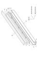
次に、図2は、照明装置300の外観図である。照明装置300の側面にコネクタ20(レセプタクル)及びコネクタ21(レセプタクル)が設けられている。コネクタ20又はコネクタ21は、電源装置200のコネクタとケーブル等により接続される。このように接続されることにより、電源装置200から照明装置300に電源(電力)が供給され、電源装置200と照明装置300との間で制御コマンドを送受信することできる。
<<<Overall Configuration of
Next, FIG. 2 is an external view of the
コネクタ20は、端部基板310に電気的に接続され、コネクタ21は、端部基板320に電気的に接続される。
本明細書において、説明の便宜上、電源装置200のCPU201が照明装置300へコマンドを送信すると記載したり、照明装置300が電源装置200のCPU201へコマンドを送信すると記載したりする場合があるが、詳細には、電源装置200のCPU201が送信するコマンドは、LED基板350のCPU351へ送信されることを意味し、LED基板350のCPU351が送信するコマンドは、電源装置200のCPU201へ送信されることを意味する。
In this specification, for convenience of explanation, it may be described that the CPU 201 of the
照明装置300には、開口部である照射部10が形成されており、LEDから発せられた光は、照射部10から射出される。
The
次に、図3を参照しながら照明装置300の全体構成を説明する。照明装置300は、筐体30と、複数のLED基板350と、複数のLEDと、ロッドレンズ40と、ディフューザレンズ50とを主に備える。詳細には、照明装置300は、4枚のLED基板を備え、1枚のLED基板には、26個のLEDが搭載されている。
<筐体30>
筐体30は、照明装置300の部品を収納し、おおよその外形を画定する。筐体30は、アルミ製であり、押し出し成形によって形成されている。
Next, the overall configuration of the
<
The
筐体30は、長手方向に長尺な溝状の形状を有する。筐体30は、底面部31と、底面部31を挟んで互いに向かい合う2つの側面部(32、33)を有する。底面部31及び2つの側面部は、長手方向に長尺で平坦な形状を有する。2つの側面部は、同じ大きさ及び形状を有し、底面部31に対して高さ方向に沿って立設され、互いに平行になるように配置されている。
The
2つの側面部の各々は、底面部31から最も離隔した最上部に、底面部31と平行に形成された天面部(34、35)を有する。
Each of the two side surface portions has a top surface portion (34, 35) formed parallel to the
<LED基板350>
LED基板350の各々には複数のLEDが搭載されており、LED基板350は複数のLEDへ、発光させるための電源(電力)を供給するとともに、CPU351により複数のLEDの点灯及び消灯の制御が行われる。
<
A plurality of LEDs are mounted on each of the
LED基板350は、アルミ基板によって構成され、薄板状の長方形状の形状を有する。LED基板350の各々には、26個のLEDが搭載されている。26個のLEDは、LED基板350の長手方向に沿って直線状に配置されている。
The
LED基板350は、LEDが上向き(Z方向)に向くように取り付けられている。筐体30には複数枚のLED基板350が搭載されている。複数枚のLED基板350は、筐体30の長手方向(Y方向)に沿って、互いに隣り合うLED基板350が密着するように配置仮想直線L1上に沿って配置されている。
The
<LED>
LEDは、照明装置300から光を発するための光源である。前述したように、26個のLEDが、LED基板350に搭載されている。LED基板350の26個のLEDは、Z方向(上向き)に向かって光を発する。
<LED>
The LED is a light source for emitting light from
<ロッドレンズ40>
ロッドレンズ40は、LEDから発せられた光を集光する。ロッドレンズ40は、アクリル製で、長尺な円筒状の形状を有する。
<
A
ロッドレンズ40は、LEDから離隔した上方に、かつ、LEDの配置仮想直線L1とロッドレンズ40の中心軸線L2とが平行になるように配置されている。
The
ロッドレンズ40は、レンズステイ(不図示)によって左右から挟持され、4本のレンズステイを介して筐体30に固定されている。
The
<ディフューザレンズ50>
ディフューザレンズ50は、ロッドレンズ40を透過する光を拡散させるための拡散板である。
<
The
ディフューザレンズ50は、ロッドレンズ40の長手方向に沿って配置されている。具体的には、ディフューザレンズ50が、ロッドレンズ40から離隔した上方に、かつ、ディフューザレンズ50の中心軸線L3がロッドレンズ40の中心軸線L2と平行になるように配置されている。
The
ディフューザレンズ50の表面には、微小なレンズアレイが形成されている。ディフューザレンズ50の表面には、長尺な溝状の領域と長尺な畝状の領域とが、隣り合うように交互に形成されている。溝状の領域の長手方向及び畝状の領域の長手方向は、おおよそ幅方向である。溝状の領域と畝状の領域とによって、微小でランダムな凹凸が繰り返され、微小な凹凸は、微小なレンズアレイとして機能する。
A minute lens array is formed on the surface of the
ディフューザレンズ50は、レンズアレイの拡散機能により、入射した光を所望する拡散角(配光角)で光を屈折させて拡散整形する。ディフューザレンズ50は、一定の方向の拡散を他の方向よりも強く拡散する楕円拡散する。具体的には、ディフューザレンズ50は、長さ方向(長手方向)の拡散は、幅方向(短手方向)よりも強く拡散する。
The
<<<光の進行状態>>>
LEDから発せられた光は、ロッドレンズ40を通過した後、ディフューザレンズ50によって拡散されて照明装置300から出射される。以下では、幅方向(短手方向)成分の光と、長さ方向(長手方向)成分の光とについて、光の進行を説明する。
<<<Progress of light>>>
After passing through the
<幅方向(短手方向)成分の光の進行>
LEDから発せられた光は、広がりつつロッドレンズ40に入射する。ロッドレンズ40に入射した光は、ロッドレンズ40の屈折率に応じて屈折して、ロッドレンズ40の内部を進行する。ロッドレンズ40の内部を進行した光は、ロッドレンズ40の屈折率に応じて屈折してロッドレンズ40から出射する。光の進行方向は、ロッドレンズ40に入射した箇所の入射角により定まり、ロッドレンズ40は、幅方向(短手方向)成分については、凸レンズとして機能し、ロッドレンズ40に入射した光を集光する。LEDから発せられた光は、ロッドレンズ40によって集光されて、ロッドレンズ40から出射する。
<Advancement of Light in Width Direction (Transverse Direction)>
The light emitted from the LED enters the
ロッドレンズ40によって集光された光は、ディフューザレンズ50に入射する。ディフューザレンズ50は、長さ方向(長手方向)の拡散は、幅方向(短手方向)よりも強く拡散する。したがって、幅方向(短手方向)については、光はあまり拡散されずにディフューザレンズ50から出射される。すなわち、幅方向(短手方向)の成分については、ロッドレンズ40によって集光された光が照明装置300から出射される。
Light condensed by the
<長さ方向(長手方向)成分の光の進行>
図4は、長さ方向(長手方向)成分に関する光の進行を示す概略図である。LEDから発せられた光は、広がりつつロッドレンズ40に入射する。ロッドレンズ40に入射した光は、ロッドレンズ40の屈折率に応じて屈折して、ロッドレンズ40の内部を進行し、ロッドレンズ40の屈折率に応じて屈折してロッドレンズ40から出射する。長さ方向(長手方向)成分については、ロッドレンズ40は、集光機能を有さず、LEDから発せられた光は、平行な板ガラスと同様の屈折の過程を経て、ロッドレンズ40から出射する。
<Progress of light in the length direction (longitudinal direction) component>
FIG. 4 is a schematic diagram showing light traveling with respect to the length direction (longitudinal direction) component. The light emitted from the LED enters the
ロッドレンズ40によって集光された光は、ディフューザレンズ50に入射する。ディフューザレンズ50は、長さ方向(長手方向)の拡散は、幅方向(短手方向)よりも強く拡散する。したがって、図4に示すように、長さ方向(長手方向)成分の光は、ディフューザレンズ50の表面に形成されたレンズアレイの形状や大きさに応じて拡散され、ディフューザレンズ50から出射される。すなわち、幅方向(短手方向)の成分については、ロッドレンズ40によって集光された光が照明装置300から出射される。
Light condensed by the
このように、幅方向(短手方向)成分は、ロッドレンズ40によって集光された光となり、長さ方向(長手方向)成分は、ディフューザレンズ50によって拡散された光となり、照明装置300から出射される。
In this way, the width direction (short direction) component becomes light condensed by the
<<<回路図>>>
図5は、照明システムの全体の回路の構成の概略を示すブロック図である。簡便のため、図5では、代表的にLED基板350-1とLED基板350-2を照明装置300に示し、外部機器100は省略した。なお、前述したように、LED基板350-1及びLED基板350-2は、同じ構成を有するが、図5では、LED基板350-2については、I/Oポート359-2のみを示し、他の構成は省いた。LED基板350には、CPU351と、DAC-a355aと、DAC-b355bと、LED-a356a、LED-b356bと、I/Oポート359と、フォトダイオード(PD)と、サーミスタ(TH1、TH2、TH3)と、A/Dコンバータと、定電流回路と、電流増幅回路とが搭載されている。電流増幅回路は、レンジ切替部を有する。
<<<circuit diagram>>>
FIG. 5 is a block diagram showing an outline of the overall circuit configuration of the lighting system. For the sake of simplicity, FIG. 5 representatively shows LED board 350-1 and LED board 350-2 in
電源装置200から出力された制御信号(パルス信号)はLED基板350-1へ入力される。LED基板350-1には、オンオフスイッチ360-1(アナログスイッチ)が設けられている。本実施形態では、電源装置200から出力された制御信号(パルス信号)は、LED基板350-1のCPU351-1へ入力されると共に、LED基板350-1のオンオフスイッチ360-1へも供給される。制御信号(パルス信号)がハイレベルのときにはオンオフスイッチ360-1が導通状態になり、DAC(DAC-a355a-1、DAC-b355b-1)によって変換された電圧信号が定電流回路へと入力される。制御信号(パルス信号)がローレベルのときにはオンオフスイッチ360-1が非導通状態(遮断状態)になり、DAC(DAC-a355a-1、DAC-b355b-1)によって変換された電圧信号は定電流回路へ入力されない。
A control signal (pulse signal) output from the
電源装置200のCPU201から送信された制御コマンドは、端部基板310又は端部基板320を介してLED基板350-1へ入力される。制御コマンドは、LED基板350-1のI/Oポート359-1を介してCPU351-1へ入力される。制御コマンドは、照明装置300のLEDの発光の明るさを制御するため入力値や、LEDを点灯させるための点灯コマンドなどの各種の値やコマンドを含む。操作者は、電源装置200の操作部207を操作して、LEDから発する光の明るさを調整することができる。LEDから発する光の明るさの調整に用いる値を入力値という。操作者が操作部207を操作することで、電源装置200のCPU201に入力値を入力することができる。入力値は制御コマンドに含まれ、電源装置200からCPU351(351-1、351-2、351-3、351-4)へ入力される。
A control command transmitted from the CPU 201 of the
LED基板350-1のCPU350-1は、受信した入力値をDAC値(デジタル値)に変換する(詳細は後述する)。DAC値を示すデジタル信号は、DAC(DAC-a355a-1、DAC-b355b-1)へ出力される。DAC(DAC-a355a-1、DAC-b355b-1)は、DAC値を示すデジタル信号を、DAC値を示すアナログ信号に変換する。 CPU 350-1 of LED board 350-1 converts the received input value into a DAC value (digital value) (details will be described later). A digital signal representing the DAC value is output to the DACs (DAC-a 355a-1, DAC-b 355b-1). The DACs (DAC-a 355a-1, DAC-b 355b-1) convert digital signals representing DAC values into analog signals representing DAC values.
DAC-a355a-1は、LED基板350-1に搭載されている26個のLEDのうちの第1の13個分のLED群のLED-a356a-1を制御するためのDAC値(デジタル信号)を電圧値(DAC値を示すアナログ信号)に変換し、DAC-b355b-1は、LED基板350-1に搭載されている26個のLEDのうちの第2の13個分のLED群のLED-b356b-1を制御するためのDAC値(デジタル信号)を電圧値(DAC値を示すアナログ信号)に変換する。 The DAC-a355a-1 is a DAC value (digital signal) for controlling the LED-a356a-1 of the first 13 LED group out of the 26 LEDs mounted on the LED board 350-1. to a voltage value (an analog signal indicating a DAC value), and the DAC-b 355b-1 converts the second 13 LEDs of the 26 LEDs mounted on the LED board 350-1 to LED -Converts the DAC value (digital signal) for controlling b356b-1 into a voltage value (analog signal indicating the DAC value).
このように、電源装置200から各LED基板350のCPU359へ単一の値の入力値が送信される。後述するように各LED基板350に搭載されたLED群には個体差によって発光の明るさにバラつきがあるため、各LED基板350のCPU359は、このバラつきを軽減するために後述するような一次関数(式1、式2参照)に基づいてDAC値を算出する。つまり、入力値は、単一の値であるが、各LED基板350で算出されるDAC値は、各LED基板350に搭載されたLED群の電気的特性や光学的特性に応じた値となる。電気的特性や光学的特性に応じたDAC値を用いてLEDを発光させることで、各LED基板350のLEDから発する光の明るさを均一にすることができる。そして、各LED基板350のCPU359は、DAC値を示すデジタル信号をDAC(DAC-a355a、DAC-b355b)へ出力し、LED群を発光させるために、DACにより、DAC値を示すデジタル信号が、DAC値を示すアナログ信号に変換される。具体的には、DAC値を示すアナログの電圧信号(以下、DAC値を示す電圧信号)に変換される。
Thus, a single input value is sent from the
DAC(DAC-a355a-1、DAC-b355b-1)から出力されたDAC値を示す電圧信号は、定電流回路へ入力されて、電流に変換される。定電流回路は、例えば、オペアンプ(演算増幅器)や抵抗などの素子からなり、抵抗値で定まる増幅率で電圧信号を電流信号に変換する。つまり、定電流回路は、DAC値を示す電圧信号を、DAC値に対応する電流に変換する。定電流回路から出力された電流は、電流増幅回路へ入力されて増幅される。電流増幅回路は、トランジスタやFETなどの増幅素子からなり、定電流回路から出力された電流を所望する増幅率で増幅する。電流増幅回路によって増幅された電流は、LEDを駆動するための駆動電流としてLED群(LED-a356a-1、LED-b356b-1)へ入力される。LED群(LED-a356a-1、LED-b356b-1)は、駆動電流に応じた明るさで発光する。
A voltage signal indicating a DAC value output from the DACs (DAC-a355a-1, DAC-b355b-1) is input to a constant current circuit and converted into current. The constant current circuit is composed of elements such as an operational amplifier (operational amplifier) and resistors, and converts a voltage signal into a current signal with an amplification factor determined by a resistance value. That is, the constant current circuit converts the voltage signal indicating the DAC value into a current corresponding to the DAC value. The current output from the constant current circuit is input to the current amplifier circuit and amplified. The current amplifying circuit is composed of amplifying elements such as transistors and FETs, and amplifies the current output from the constant current circuit with a desired amplification factor. The current amplified by the current amplifier circuit is input to the LED group (LED-a 356a-1, LED-
LED群の第1の端部FTは、電源装置200に接続されている。LED群の第2の端部STは、電流増幅回路に接続されており、前述したように、電流増幅回路からLED群に駆動電流が供給される。LED群の第1の端部FTは、電源電圧監視回路に接続されている。
A first end FT of the LED group is connected to the
LED基板350-1には、A/Dコンバータが設けられている。A/Dコンバータは、アナログ信号をデジタル信号に変換する。A/Dコンバータは、LED基板350-1のCPU351-1と接続されている。A/Dコンバータによって変換されたデジタル信号は、CPU351-1に入力される。A/Dコンバータには、電源電圧監視回路と、フォトダイオードPD(LED群から発せられた光の照度を検出する)と、サーミスタTH1(第1の13個分のLED群(LED-a356a-1)の温度を検出する)と、サーミスタTH2(第2の13個分のLED群(LED-b356b-1)の温度を検出する)とが、接続されている。電源電圧監視回路は、抵抗値の大きい抵抗などから構成され、LED群に供給される駆動電流の電流値を、所定の電圧範囲内に含まれる電圧値に変換して、A/Dコンバータに出力する。これにより、電源装置200から出力される電源電圧が適切なものであるか否かを判断することができる。フォトダイオードPDは、LED群から発せられた光の照度が適切であるか否かを判断することができる。サーミスタTH1及びサーミスタTH2は、LED群の温度が適切であるか否かを判断することができる。
An A/D converter is provided on the LED board 350-1. An A/D converter converts an analog signal into a digital signal. The A/D converter is connected to the CPU 351-1 of the LED board 350-1. A digital signal converted by the A/D converter is input to the CPU 351-1. The A/D converter includes a power supply voltage monitoring circuit, a photodiode PD (which detects the illuminance of light emitted from the LED group), and a thermistor TH1 (the first group of 13 LEDs (LED-a356a-1 )) and the thermistor TH2 (which detects the temperature of the second group of 13 LEDs (LED-b356b-1)) are connected. The power supply voltage monitoring circuit consists of a resistor with a large resistance value, etc., converts the current value of the drive current supplied to the LED group into a voltage value within a predetermined voltage range, and outputs it to the A/D converter. do. Accordingly, it can be determined whether the power supply voltage output from the
電圧電流交換回路は、I/Oポート359-1を介してLED基板350-1のCPU351-1に接続されており、オープンエラー等の検出が可能となっている。 The voltage-current exchange circuit is connected to the CPU 351-1 of the LED board 350-1 via the I/O port 359-1, and is capable of detecting an open error or the like.
サーミスタTH3(LED基板の温度を検出する)は、I/Oポート359-1を介してLED基板350-1のCPU351-1に接続されている。 Thermistor TH3 (which detects the temperature of the LED board) is connected to CPU 351-1 of LED board 350-1 via I/O port 359-1.
レンジ切替回路は、選択可能な複数の抵抗を有しており、選択する抵抗の組合せに応じて抵抗値を切り替えて駆動電流の電流範囲を切り替えることで、LED群の照度の範囲(照度レンジ)を変更可能に構成されている。例えば、複数の抵抗を直列や並列に接続して、選択する抵抗の組合せを変更することで、駆動電流の電流範囲を切り替えて、LED群の照度の範囲(照度レンジ)を変更することができる。照度レンジは、操作者が電源装置200の操作部207(例えば、ボリューム270A、スイッチ270B)を操作することで切り替えることができる。
The range switching circuit has a plurality of selectable resistors, and switches the current range of the drive current by switching the resistance value according to the combination of resistors to be selected, thereby changing the illuminance range of the LED group (illuminance range). is configured to be changeable. For example, by connecting multiple resistors in series or in parallel and changing the combination of resistors to be selected, it is possible to switch the current range of the drive current and change the illuminance range (illuminance range) of the LED group. . The illuminance range can be switched by the operator operating the operation unit 207 (for example, the volume 270A and the switch 270B) of the
I/Oポート359-1は、次のLED基板350-2のI/Oポート359-2と接続されており、後述するアドレス割り振りコマンドの送信の際に用いる。 The I/O port 359-1 is connected to the I/O port 359-2 of the next LED board 350-2, and is used when transmitting an address allocation command, which will be described later.
<<<照明モード>>>
図6は、照明装置300におけるLED群による照明のタイミングチャートである。図6に示すタイムチャートの横軸は時間(時刻)Tであり、縦軸はLEDから発せられる光の照度である。照明装置300は、検査中は常にLED群を点灯するよう構成されており、図6に示す例では、0から最大値の間の一定の照度で連続して点灯していることを示している。操作者は、電源装置200の操作部207(例えば、ボリューム270A)を操作することによって、所望する発光の明るさを設定することが可能であり、照明装置300は、操作者により設定された入力値に応じた明るさでLED群を常時点灯する。LEDの点灯時の明るさ(照度)の制御は、電源装置200のCPU201から送信される制御コマンドによって行われる。
<<<Lighting Mode>>>
FIG. 6 is a timing chart of lighting by the LED group in
照明モードは、操作者により電源装置200で設定された入力値に応じてDAC値を算出し、DAC値に対応する明るさ(照度)の光を照明装置300のLED群が常に出力するモードである。照明モードでは、電源装置200のCPU201から送信される制御コマンドのみによって照明装置300のLED群が制御される。照明モードで用いる制御コマンドは、LED群から発する光の明るさ(照度)に対応する入力値(全照度モードでは0~3000、その他の照度モードでは0~1000)を含み、当該コマンドに含まれる入力値はEEPROM354に記憶される。
The lighting mode is a mode in which a DAC value is calculated according to an input value set by the operator in the
具体的には、操作者が電源装置200の操作部207(例えば、ボリューム207A)を操作することによって入力値を設定すると、設定された入力値を含むコマンドが電源装置200のCPU201から照明装置300のLED基板350のCPU351へ送信される。LED基板350のCPU351は、受信したコマンドに含まれる入力値をEEPROM354に記憶する。CPU351により入力値に基づいてLEDの光学的特性などに合わせたDAC値を算出し、DAC値に対応する駆動電流によってLEDを駆動することによって、入力値に対応する均一な明るさでLED群から光が発せられる。
Specifically, when an operator sets an input value by operating the operation unit 207 (for example, volume 207A) of the
電源装置200のCPU201から送信されたコマンドは、照明装置300の複数のLED基板350(350-1、350-2、350-3、350-4)へ並列に、言い換えると、同時に入力される。そのため、複数のLED基板350のCPU351は、同じタイミングでLED群の出力制御を行うことができる。
Commands transmitted from the CPU 201 of the
<<<電源装置200の制御処理>>>
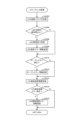
図7は、電源装置200における電源装置制御処理のフローチャートである。まず、電源装置200のCPU201は、ステップ702で、初期化するか否かを判定する。
<<<control processing of
FIG. 7 is a flowchart of power supply control processing in
操作者が操作部207を操作することにより初期化することが決定されると、初期化が実行される。例えば、後述するメニュー設定処理が呼び出されて、初期化が実行されることを決定することができる。 When the operator operates the operation unit 207 to decide to initialize, the initialization is executed. For example, it can be determined that a menu setting process, which will be described later, is called to perform initialization.
ステップ702でYesの場合、ステップ704で、電源装置200のCPU201は、初期化処理を行う。ステップ702でNoの場合、ステップ706の処理へ移行する。
In the case of Yes in step 702, in step 704, the CPU 201 of the
初期化処理(ステップ704)では、電源装置200のCPU201は、RAM203の記憶情報を初期化する。具体的には、後述するアドレス割り振り処理の終了コマンドを受信したことを示す情報(例えば、受信フラグ)等を初期化(デフォルトに戻す)し、照明装置300のLED基板350のCPU351へ初期化コマンドを送信する。
In initialization processing (step 704 ), the CPU 201 of the
次に、ステップ706で、電源装置200のCPU201は、LED基板350のCPU351のアドレス割り振り処理が終了していることを記憶しているか否かを判定する。
Next, in step 706, the CPU 201 of the
ステップ706でNoの場合、つまり、LED基板350のCPU351のアドレス割り振り処理が終了していない場合、ステップ708で、電源装置200のCPU201は、LED基板350のCPU351がアドレス番号を記憶するためのアドレス番号割り振りコマンドを照明装置300へ送信する。
If No in step 706, that is, if the address allocation process of the CPU 351 of the
ステップ706でYesの場合、つまり、LED基板350のCPU351のアドレス割り振り処理が終了している場合、ステップ710の処理へ移行する。
If Yes in step 706 , that is, if the address allocation process of the CPU 351 of the
次に、ステップ710で、電源装置200のCPU201は、LED基板350のうちの最後のLED基板のCPU(例えば、LED基板350-4のCPU351-4)からアドレス割り振り処理の終了コマンドを受信済みであるか否かを判定する。
Next, in step 710, the CPU 201 of the
ステップ710でNoの場合、つまり、全てのLED基板350のCPU351のアドレス割り振り処理が終了していない場合は、ステップ710の処理を繰り返し、全てのLED基板350のCPU351のアドレス割り振り処理が終了するまで待機する。
In the case of No in step 710, that is, when the address allocation processing of the CPUs 351 of all the
ステップ710でYesの場合、つまり、全てのLED基板350のCPU351のアドレス割り振り処理が終了した場合は、ステップ712の処理へ移行する。
In the case of Yes in step 710 , that is, when the address allocation processing of the CPUs 351 of all the
次に、ステップ712で、電源装置200のCPU201は、操作者によってメニュー操作が行われたか否かを判定する。
Next, at step 712, the CPU 201 of the
ステップ712でYesの場合、ステップ714で、電源装置200のCPU201は、メニュー設定処理を行う。ステップ712でNoの場合、ステップ716の処理へ移行する。
In the case of Yes in step 712, in step 714, the CPU 201 of the
メニュー設定処理では、電源装置200のCPU201は、操作者の電源装置200の操作結果をEEPROM204に記憶する。具体的には、操作者による操作には、入力値の変更、照度レンジの切り替え、調光調整開始等があり、これらの操作結果をEEPROM204に記憶する。メニュー設定に関する情報を電源装置側(EEPROM204)で記憶しておくことで、電源立ち上げの際に照明装置300を前回の設定状況で復帰させることができる。
In the menu setting process, the CPU 201 of the
操作者により検査停止や検査一時停止等のメニュー操作が行われた場合は、当該メニュー設定処理で照明装置300へその旨を示すコマンド(検査停止コマンド、検査一時停止コマンド等)を送信する。
When the operator performs a menu operation such as inspection stop or inspection suspension, a command indicating that effect (inspection stop command, inspection suspension command, etc.) is transmitted to the
操作者が外部機器100により検査停止の操作を行った場合は、外部機器100から電源装置200へ検査停止コマンドが送信され、電源装置200のCPU201は、当該メニュー設定処理で検査停止コマンドを照明装置300へ送信する。
When the operator operates the
次に、ステップ716で、電源装置200のCPU201は、メニュー操作が行われ、調光調整開始の操作が行われたか否かを判定する。
Next, in step 716, the CPU 201 of the
ステップ716でYesの場合、ステップ1800で、電源装置200のCPU201は、後述する電源側調光調整処理を実行する。
In the case of Yes in step 716, in step 1800, the CPU 201 of the
ステップ716でNoの場合、ステップ720の処理へ移行する。 If No in step 716 , the process proceeds to step 720 .
次に、ステップ720で、電源装置200のCPU201は、メニュー操作が行われ、照度の変更(入力値の変更)が行われたか否かを判定する。
Next, in step 720, the CPU 201 of the
ステップ720でYesの場合、ステップ722で、電源装置200のCPU201は、照明装置300へ後述する照度コマンドを送信する。
In the case of Yes at step 720 , at step 722 , the CPU 201 of the
ステップ720でNoの場合、ステップ724の処理へ移行する。照度コマンドは、入力値や明るさや明暗度を示すが、いずれの照度レンジであるかを含めたコマンドとしてもよい。 If No in step 720 , the process proceeds to step 724 . The illuminance command indicates an input value, brightness, and intensity, but may be a command including which illuminance range it is.
次に、ステップ724で、電源装置200のCPU201は、メニュー操作が行われ、照度レンジの切り替えが行われたか否かを判定する。
Next, in step 724, the CPU 201 of the
ステップ724でYesの場合、ステップ726で、電源装置200のCPU201は、照明装置300へ変更後の照度レンジ(後述する全照度モード、低照度モード、中照度モード、高照度モード)を示す照度レンジコマンドを送信する。
In the case of Yes in step 724, in step 726, the CPU 201 of the
ステップ724でNoの場合、ステップ728の処理へ移行する。 If No in step 724 , the process proceeds to step 728 .
操作者は照度レンジを切り替えることで、照明装置300のLED群が所望する照度範囲内で光を発するように設定することができる。
By switching the illuminance range, the operator can set the LED group of the
次に、ステップ728で、電源装置200のCPU201は、コマンド受信処理を行い、ステップ730の処理へ移行する。
Next, at step 728 , the CPU 201 of the
コマンド受信処理では、電源装置200のCPU201は、外部機器100又は照明装置300から送信されたコマンドを受信し、受信したコマンドに基づいてRAM203又はEEPROM204に情報を記憶する。
In the command reception process, the CPU 201 of the
次に、ステップ730で、電源装置200のCPU201は、エラーチェック処理を行う。
Next, in step 730, the CPU 201 of the
エラーチェック処理(ステップ730)では、電源装置200のCPU201は、照明装置300の各CPUとの通信チェック、電源装置200内の通信異常(電源異常)チェック等を行う。
In the error check process (step 730), the CPU 201 of the
次に、ステップ732で、電源装置200のCPU201は、ディスプレイ表示処理を行い、ステップ732の処理が終了すると、ステップ702の処理へ戻る。
Next, in step 732, the CPU 201 of the
ディスプレイ表示処理では、電源装置200のCPU201は、ディスプレイ206に各種の情報を表示するための処理を行う。具体的には、メニュー設定処理の操作結果に基づいて照明モード、入力値や明暗度等の表示、その他にLED基板温度、エラー(LED温度異常、オープンエラー、通信異常等)の表示等を行う。
In the display display processing, the CPU 201 of the
<<<照明装置300の制御処理>>>
<<照明制御処理>>
図8は、照明装置300における照明制御処理のフローチャートである。まず、ステップ902で、LED基板350のCPU351は、後述するアドレス割り振り処理が終了済みではないか否かを判定する。
<<<Control Processing of
<<Lighting control processing>>
FIG. 8 is a flowchart of lighting control processing in
ステップ902でYesの場合、つまり、アドレス割り振り処理がまだ行われていない場合には、ステップ1100で、LED基板350のCPU351は、アドレス割り振り処理を行う。
If Yes in step 902 , that is, if the address allocation process has not yet been performed, in step 1100 the CPU 351 of the
ステップ902でNoの場合、つまり、アドレス割り振り処理が既に行われている場合には、ステップ904の処理へ移行する。 If No in step 902 , that is, if the address allocation process has already been performed, the process proceeds to step 904 .
次に、ステップ904で、LED基板350のCPU351は、調光調整済みではないか否か、つまり、後述する照明側調光調整処理が終了済みではないか否かを判定する。
Next, in step 904, the CPU 351 of the
ステップ904でYesの場合、ステップ1900で、LED基板350のCPU351は、照明側調光調整処理を行う。
In the case of Yes in step 904, in step 1900, the CPU 351 of the
ステップ1900の処理が終了すると、ステップ906の処理へ移行する。 When the process of step 1900 ends, the process proceeds to step 906 .
ステップ904でNoの場合、つまり、照明側調光調整処理が既に行われている場合には、ステップ906の処理へ移行する。 If No in step 904 , that is, if lighting-side dimming adjustment processing has already been performed, the process proceeds to step 906 .
次に、ステップ906で、照明装置300のLED基板350のCPU351は、コマンド受信処理を行う。
Next, in step 906, the CPU 351 of the
コマンド受信処理では、LED基板350のCPU351は、電源装置200のCPU201から送信されたコマンドを受信する。例えば、LED基板350-1のCPU351-1やLED基板350-2のCPU351-2は、電源装置200のCPU201から送信されたコマンドを受信する。操作者が外部機器100又は電源装置200により、検査の停止操作や一時停止の操作を行うと、外部機器100又は電源装置200のCPU201から検査停止コマンドや検査一時停止コマンドが送信され、LED基板350のCPU351は、検査停止コマンドを受信した場合には、検査を停止又は一時停止する処理を行う。例えば、LEDの消灯等を行う。
In the command reception process, CPU 351 of
次に、ステップ908で、LED基板350のCPU351は、初期化するか否か、言い換えると、コマンド受信処理により初期化コマンドを受信したか否かを判定する。
Next, at step 908, the CPU 351 of the
ステップ908でYesの場合、ステップ910で、LED基板350のCPU351は、後述する初期化処理を行う。ステップ908でNoの場合、ステップ914の処理へ移行する。
In the case of Yes in step 908, in step 910, the CPU 351 of the
初期化処理(ステップ910)では、LED基板350のCPU351は、RAM353の記憶情報を初期化する。具体的には、アドレス割り振り処理におけるアドレス番号等を初期化する。
In the initialization process (step 910 ), the CPU 351 of the
次に、ステップ914で、LED基板350のCPU351は、照度コマンドを受信したか否か、言い換えると、照度の変更(明るさの設定)が行われたか否かを判定する。
Next, in step 914, the CPU 351 of the
ステップ914でYesの場合、ステップ916で、LED基板350のCPU351は、照度コマンドに基づいてEEPROM354の照度記憶テーブルに入力値を記憶する。より詳細には、照度レンジに応じて入力値を記憶する。
If Yes at step 914, at step 916, the CPU 351 of the
ステップ914でNoの場合、ステップ918の処理へ移行する。 If No in step 914 , the process proceeds to step 918 .
次に、ステップ918で、LED基板350のCPU351は、照度レンジコマンドを受信したか否か、言い換えると、照度レンジの変更が行われたか否かを判定する。
Next, at step 918, the CPU 351 of the
ステップ918でYesの場合、ステップ920で、LED基板350のCPU351は、後述する照度レンジ切替処理を行い、ステップ922の処理へ移行する。ステップ918でNoの場合、ステップ922の処理へ移行する。
If Yes at step 918 , at step 920 , the CPU 351 of the
照度レンジ切替処理では、LED基板350のCPU351は、コマンド受信処理で受信した照度レンジコマンドが全照度モードを示すコマンドであれば、照度レンジを全照度モードに変更し、コマンド受信処理で受信した照度レンジコマンドが低照度モードを示すコマンドであれば、照度レンジを低照度モードに変更し、コマンド受信処理で受信した照度レンジコマンドが中照度モードを示すコマンドであれば、照度レンジを中照度モードに変更し、コマンド受信処理で受信した照度レンジコマンドが高照度モードを示すコマンドであれば、照度レンジを高照度モードに変更する。
In the illuminance range switching process, if the illuminance range command received in the command reception process is a command indicating the full illuminance mode, the CPU 351 of the
次に、ステップ921で、後述するDAC値算出処理を実行する。DAC値算出処理では、設定された照度レンジに対応する入力値を用いてDAC値を算出する。なお、前述した通り、全照度モードにおける入力値の範囲(0~3000)と、他の照明モード(低照度モード、中照度モード、高照度モード)における入力値の範囲(0~1000)とは異なっている。このため、全照度モードから他の照明モードに変更された場合のデフォルトの入力値は、全照度モードで設定していた入力値の1/3とする。反対に、他の照明モードから全照度モードに変更された場合のデフォルト入力値は、他の照明モードで設定していた入力値の3倍とする。 Next, in step 921, DAC value calculation processing, which will be described later, is executed. In the DAC value calculation process, the DAC value is calculated using the input value corresponding to the set illuminance range. As described above, the input value range (0 to 3000) in full illumination mode and the input value range (0 to 1000) in other illumination modes (low illumination mode, medium illumination mode, high illumination mode) different. Therefore, the default input value when the full illumination mode is changed to another illumination mode is set to ⅓ of the input value set in the full illumination mode. Conversely, the default input value when changing from another illumination mode to the full illumination mode is three times the input value set in the other illumination mode.
このようにすることで、全照度モードと他の照明モードで入力値の範囲が異なる場合であっても、ボリューム207Aの回転可能な範囲を一定にすることができる。 By doing so, even if the range of input values differs between the full illumination mode and the other lighting modes, the rotatable range of the volume 207A can be kept constant.
次に、ステップ922で、LED基板350のCPU351は、EPPROM354の記憶情報を読み出して、LEDの出力処理(照射制御)を行う。
Next, in step 922, the CPU 351 of the
次に、ステップ2400で、LED基板350のCPU351は、後述するエラーチェック処理を行う。
Next, at step 2400, the CPU 351 of the
次に、ステップ924で、LED基板350のCPU351は、電源装置200のCPU201へコマンドを送信するためのコマンド送信処理を実行する。例えば、LED温度エラー情報等を送信する。
Next, at step 924 , CPU 351 of
次に、ステップ926で、LED基板350のCPU351は、検査終了とするか否か、つまり、操作者が外部機器100や電源装置200を操作して検査を終了する操作をしたか否か又は全ての検査対象物の検査が終了したか否かを判定する。
Next, in step 926, the CPU 351 of the
ステップ926でYesの場合、ステップ928で、LED基板350のCPU351は、検査終了処理(例えば、LEDを消灯する等)を実行し、検査を終了する。
In the case of Yes in step 926, in step 928, the CPU 351 of the
ステップ926でNoの場合、ステップ906の処理へ移行する。 If No in step 926 , the process proceeds to step 906 .
<<アドレス割り振り処理の概要>>
次に、図9を用いてアドレス割り振り処理の概要を説明する。アドレス割り振り処理は、照明装置300のLED基板350に搭載されたLED群を識別するためにそれぞれ何番目のLED群であるのかを、それぞれのLED群が搭載されたLED基板350のCPU351が登録(記憶)するための処理である。アドレス割り振り処理は、電源装置200及び照明装置300の起動毎に開始する。電源装置200は、電源が投入されると、照明装置300がアドレス割り振り処理を開始するためのアドレス番号割り振りコマンドを照明装置300に送信する。照明装置300のLED基板350のCPU351は、アドレス番号割り振りコマンドを受信するとアドレス割り振り処理を実行する。照明装置300の複数のLED基板のCPUは、所定の順番でアドレス割り振りコマンドを受信し、所定の順番でアドレス割り振り処理を実行するように構成されている。
<<Overview of Address Allocation Process>>
Next, an outline of address allocation processing will be described with reference to FIG. In order to identify the LED groups mounted on the
照明装置300にはコマンドラインCLが設けられており、図示していないが電源装置200のCPU201から送信されたコマンドは、コマンドラインCLにより端部基板(310、320)を介してLED基板350のCPU351に入力可能である。LED基板350のCPU351はコマンドラインCLによりコマンドを送信可能である。図5に示したように、制御信号(パルス信号)ラインPLが設けられており、電源装置200のCPU201から出力された制御信号は、制御信号ラインPLにより端部基板(310、320)を介してLED基板350のCPU351に入力される。制御信号ラインPLには、波形整形回路(例えば、シュミットバッファ)が設けられ、制御信号の波形が安定するように構成されてもよい。
The
隣り合うLED基板350のI/Oポート359のポート1とポート2とが接続されている。例えば、LED基板350-1のI/Oポート359-1のポート2は、LED基板350-2のI/Oポート359-2のポート1に接続されている。
LED基板350のI/Oポート359のポート2は、起動時には、入力ポートとして機能する。LED基板350のI/Oポート359のポート2は、アドレス番号割り振りコマンドを受信した後は、出力ポートとして機能する。
コマンドラインCLは、LED基板350-1~LED基板350-4に並列に接続されており、電源装置200から送信されたコマンドは、LED基板350-1~LED基板350-4のCPU351は、ほぼ同時に受信することが可能となっているが、アドレス割り振りコマンドについては、LED基板350のI/Oポート359のポート1がLOWレベルとなっているLED基板350のCPU351のみが受信する。
The command line CL is connected in parallel to the LED boards 350-1 to 350-4. Although it is possible to receive them at the same time, only the CPU 351 of the
LED基板350-1のCPU351-1はアドレス割り振りコマンドを受信した後、アドレス割り振りコマンドを更新してコマンドラインCLへ出力する。出力されたアドレス割り振りコマンドは、ポート1がLOWレベルとなっていると判断した他のLED基板のCPU(LED基板350-1のCPU351-1とは異なるLED基板のCPU)が受信する。例えば、LED基板350-2のCPU351-2が、ポート1がLOWレベルとなっていると判断した場合、LED基板350-2のCPU351-2はアドレス割り振りコマンドを受信する。LED基板350-2のCPU351-2はアドレス割り振りコマンドを受信した後、アドレス割り振りコマンドを更新してコマンドラインCLへ出力する。以降のLED基板のCPUについても同様である。
After receiving the address allocation command, the CPU 351-1 of the LED board 350-1 updates the address allocation command and outputs it to the command line CL. The output address allocation command is received by the CPU of another LED board (the CPU of the LED board different from the CPU 351-1 of the LED board 350-1) that has determined that the
つまり、電源装置200から送信されたアドレス割り振りコマンドは、未受信の1のLED基板のCPUが受信し、アドレス割り振りコマンドを受信したLED基板のCPUは、アドレス割り振りコマンドを記憶して更新した後、別の未受信の1のLED基板のCPUが受信可能なようにアドレス割り振りコマンドをコマンドラインへ出力する。
In other words, the address allocation command transmitted from the
具体的には、起動時には、LED基板350-1のI/Oポート359-1のポート1は端部基板310に接続されて、ポート1は、LOWレベルとなっているため、アドレス割り振りコマンドを受信可能となっている。
Specifically, at startup, the
その他のLED基板(350-2、350-3、350-4)のI/Oポート(359-2、359-3、359-4)のポート1は、一つ前のLED基板のI/Oポート(359-1、359-2、359-3)のポート2と接続されているが、制御電圧(例:5V)によりHIGHレベルとなっているため、アドレス割り振りコマンドを受信不可能となっている。
このように、起動時には、端部基板310に接続されているLED基板350-1のCPU351-1が電源装置200のCPU201からコマンドラインCLで送信されたアドレス番号割り振りコマンドを必ず最初に受信するように構成されている。
In this way, when starting up, the CPU 351-1 of the LED board 350-1 connected to the
LED基板350-1のCPU351-1は、アドレス番号割り振りコマンドを受信すると、アドレス番号割り振りコマンドの初期値のアドレス(例えば、0)から、LED基板350-1を構成するLED群の数(例えば、2つ)に応じてアドレスを登録(例えば、0、1を登録)し、LED群の数に応じてアドレスの初期値を加算(例えば、+2)して、アドレスの初期値が更新された(例えば、初期値が2となった)アドレス番号割り振りコマンドを送信する。 When the CPU 351-1 of the LED board 350-1 receives the address number allocation command, the CPU 351-1 of the LED board 350-1 calculates the number of LED groups (such as 2), the address is registered (for example, 0, 1 is registered), the initial value of the address is added (for example, +2) according to the number of LED groups, and the initial value of the address is updated ( For example, an address number allocation command with an initial value of 2 is transmitted.
LED基板350-1のCPU351-1は、アドレスを登録すると、I/Oポート359-1のポート2をHIGHレベルからLOWレベルに変更してからアドレスを加算(例えば、+2)して、アドレス番号割り振りコマンドを次のLED基板350-2のCPU351-2へ送信する。
When the address is registered, the CPU 351-1 of the LED board 350-1 changes the
LED基板350-1のCPU351-1がI/Oポート359-1のポート2をHIGHレベルからLOWレベルに変更することにより、LED基板350-2のI/Oポート359-2のポート1がLOWレベルとなるため、LED基板350-2のCPU351-2は次にアドレス番号割り振りコマンドを受信可能となる。
When the CPU 351-1 of the LED board 350-1 changes the
同様にして、LED基板350-2のCPU351-2、LED基板350-3のCPU351-3、LED基板350-4のCPU351-4がアドレス番号を登録する。最後のLED基板のCPUであるLED基板350-4のCPU351-4は、アドレス番号の登録を完了した場合、LED基板350-4のI/Oポート359-4のポート2は端部基板320に接続されているため、初めからLOWレベルになっており、HIGHレベルからLOWレベルに変更することができない。
Similarly, the CPU 351-2 of the LED board 350-2, the CPU 351-3 of the LED board 350-3, and the CPU 351-4 of the LED board 350-4 register the address numbers. When the CPU 351-4 of the LED board 350-4, which is the CPU of the last LED board, completes the registration of the address number, the
つまり、端部基板320に接続されているLED基板350-4のCPU351-4は、以降にLED基板350が接続されていないことを認識することができ、アドレス割り振り処理の終了コマンドを電源装置200へ送信する。
In other words, the CPU 351-4 of the LED board 350-4 connected to the
このように、電源装置200と照明装置300との接続向きに関わらず、つまり、照明装置300のコネクタ20と電源装置200が接続されるか、それとも、照明装置300のコネクタ21と電源装置200が接続されるかに関わらず、LED基板350-1を最初のLED基板350とし、LED基板350-4が最後のLED基板350としてLED群を制御することが可能となる。これにより、配線数を減らすことができ、ケーブルを細くすることもできる。さらに、照明装置300内の配線の取り回しを容易にすることができる。
In this way, regardless of the connection direction between the
加算する数値は、LED基板350に搭載されているLED群の数に応じて変更してもよく、例えば、LED基板350に3つのLED群が搭載されている場合には加算する数値を3にしてもよい。
The numerical value to be added may be changed according to the number of LED groups mounted on the
<<アドレス割り振り処理>>
次に、図10はアドレス割り振り処理のフローチャートである。まず、ステップ1102で、LED基板350のCPU351は、アドレス番号割り振りコマンドを受信する。
<<Address allocation process>>
Next, FIG. 10 is a flowchart of address allocation processing. First, at step 1102, the CPU 351 of the
次に、ステップ1104で、LED基板350のCPU351は、I/Oポート359のポート1がLOWレベルであるか否かを判定する。ステップ1104でNoの場合、再度ステップ1102の処理となる。
Next, at step 1104, the CPU 351 of the
ステップ1104でYesの場合、ステップ1106で、LED基板350のCPU351は、アドレス番号割り振りコマンドが示すアドレス番号の初期値から当該LED基板350のLED群のアドレス番号としてRAM353に記憶する。
If Yes at step 1104 , at step 1106 , the CPU 351 of the
LED基板350のCPU351は、アドレス番号をRAM353に記憶するため、電源断により、記憶したアドレス番号はクリアされる。つまり、LED基板350のCPU351は、起動する毎に、アドレス番号をRAM353に記憶する。
Since the CPU 351 of the
したがって、いずれかのLED基板350が故障し、故障したLED基板350を交換した場合でも、起動時にはアドレス番号が記憶されるので、故障したLED基板350のみを容易に交換することができる。また、DAC値も照明装置300側で記憶するよう構成しているため、電源装置200を交換しても照明装置300側のデータ(アドレス番号、DAC値等)は変更されず、電源装置200を交換する場合であっても、交換作業を簡便にかつ迅速に行うことができる。
Therefore, even if one of the
次に、ステップ1108で、LED基板350のCPU351は、I/Oポート359のポート2がHIGHレベルであるか否かを判定する。
Next, at step 1108, the CPU 351 of the
ステップ1108でYesの場合、ステップ1110で、LED基板350のCPU351は、I/Oポート359のポート2をLOWレベルに変更する。
If Yes at step 1108, at step 1110, the CPU 351 of the
次に、ステップ1112で、LED基板350のCPU351は、アドレス番号割り振りコマンドのアドレス番号の初期値を加算してアドレス番号割り振りコマンドを送信する。
Next, in step 1112, the CPU 351 of the
前述した通り、ステップ1112で加算される数はLED群の数に基づくように構成することができる。例えば、1つのLED基板350に2つのLED群(例えば、LED-a、LED-b)が設けられている場合には+2となり、1つのLED基板350に3つのLED群(例えば、LED-a、LED-b、LED-c)が設けられている場合には+3となる。
As previously mentioned, the number added in step 1112 can be configured to be based on the number of LED groups. For example, when two LED groups (eg, LED-a and LED-b) are provided on one
ステップ1108でNoの場合、ステップ1114で、LED基板350のCPU351は、アドレス割り振り処理が終了したことを示す終了コマンドを電源装置200のCPU201へ送信する。
If No at step 1108 , at step 1114 , the CPU 351 of the
ステップ1112、ステップ1114の処理が終了すると呼び出し元に戻る。 When the processing of steps 1112 and 1114 ends, the process returns to the caller.
なお、上述したように、ステップ1100のアドレス割り振り処理において、各LED基板のCPUは、ポート1がLOWレベルであると判断した場合にアドレス割り振りコマンドを受信する構成としたが、この構成に限られない。例えば、各LED基板のCPUは、出力されたアドレス割り振りコマンドを受信し、ポート1がLOWレベルのときにのみ受信したアドレス割り振りコマンドを用いてアドレス番号を更新する処理を行う構成としてもよい。
As described above, in the address allocation process of step 1100, the CPU of each LED board is configured to receive the address allocation command when it determines that
<<アドレス割り振り処理のまとめ>>
<コマンドラインCLの並列接続>
照明装置300のコマンドラインCLは、各LED基板350に対して並列に接続されている。このため、LED基板350の全ては、コマンドラインCLを介して、電源装置200から発せられたコマンドを同時に受信することができる。
<<Summary of address allocation processing>>
<Parallel connection of command line CL>
A command line CL of the
<ポートの接続による直列接続>
また、照明装置300において、複数のLED基板350の隣り合う2つのLED基板350の一方のLED基板350のポート1と他方のLED基板350のポート2とを接続することで、複数のLED基板が直列に接続されている。
<Series connection by connecting ports>
Further, in the
<アドレス番号の割り振り>
ポート1がLOWレベルである第1のLED基板350(割り振り許可状態のLED基板)のCPUは、アドレス割り振りコマンドを受信すると、第1のLED基板350(自分自身)にアドレス番号を割り振る。次いで、第1のLED基板350のCPUは、ポート2をLOWレベルに変更するとともに、LED群の数に応じてアドレス番号を更新して、更新したアドレス番号を示すアドレス割り振りコマンドをコマンドラインCLへ出力する。第1のLED基板350のポート2をLOWレベルに変更することで、ポート同士が接続されて隣り合う第2のLED基板350のポート1をLOWレベルに変更する。すなわち、第2のLED基板350は、割り振り禁止状態から割り振り許可状態に変更される。このため、第2のLED基板350は、第1のLED基板350からコマンドラインCLへ出力されたアドレス割り振りコマンドを受信すると、第2のLED基板350にアドレスを割り振る。
<Allocation of address numbers>
When receiving the address allocation command, the CPU of the first LED board 350 (allocation permitted state LED board) whose
第2のLED基板350は、同様に、ポート2をLOWレベルに変更するとともに、LED群の数に応じてアドレス番号を更新して、更新したアドレス番号を示すアドレス割り振りコマンドをコマンドラインCLへ出力する。このようにすることで、ポート同士が接続されて隣り合う第3のLED基板350に、更新されたアドレス番号を割り振ることができる。
The
このように、割り振り許可状態のLED基板350は、ポート同士が接続されている割り振り禁止状態のLED基板350を割り振り許可状態にするとともに、アドレス番号を更新してコマンドラインCLへ出力する。割り振り許可状態となったLED基板350が、アドレス番号を受信すると、そのアドレス番号を自分自身に割り振る。このようにして、複数のLED基板350に、順次にアドレス番号を割り振ることができる。
In this manner, the
次に、同様にポート1がLOWレベルであるLED基板のCPUがアドレス割り振りコマンドを受信することとなる。なお、ポート1がLOWレベルであるLED基板とは、前述した通りアドレス割り振りコマンドを出力したLED基板のポート2と接続されているポート1を有するLED基板である。したがって、各LED基板のポート1は順番にLOWレベルに変更され、各LED群に対するアドレス番号が割り振られることとなる。
Next, the CPU of the LED board whose
<<<照度検出システム>>>
次に、図11(a)を用いて照度検出システムの概略を説明する。図11(a)において、破線部は、照明装置300の側面部33側から見た一部破断側面図を示し、照度検出システム全体としては、ブロック図として示している。初めに、照度検出システムとは、照明装置300の製造者の出荷検査用の検査場などに設けられるシステムであり、照明装置300のLED群の間に生じる照度の誤差をなるべく均一にして照明装置300を出荷するために用いるシステムである。
<<<illuminance detection system>>>
Next, an outline of the illuminance detection system will be described with reference to FIG. 11(a). In FIG. 11(a), the dashed line indicates a partially broken side view of the
照度検出システムは、PC500(例えば、パーソナルコンピュータ)と、照度検出装置600と、電源装置200と、照明装置300とを備える。
The illuminance detection system includes a PC 500 (for example, a personal computer), an
照度検出装置600は照度検出部700を備える。照度検出部700は、照明装置300のLED群の照度を検出可能であり、LEDから照射された光を受光するための受光素子(例えば、フォトダイオード)を備えている。照度検出部700は、照明装置300の上方に配置され、照明装置300の照射部10に沿って移動可能に構成されている。照度検出部700は、照明装置300の上方の一定の高さで移動可能に構成されている。
The
照度検出部700の受光素子は、照明装置300の照射部10に向かって配置されている。受光素子は、受光した光の強度を示す信号をPC500へ出力する。PC500は、受光素子が受光した光の強度を示す信号を受信することで照度検出部700の位置を特定することができる。
The light receiving element of the
PC500は、操作者(例えば、照明装置の製造者)が操作可能であり、検査開始や検査停止の指示、照度検出部700からの検出情報の受信、照度検出装置600の制御、電源装置200とのコマンドの送受信等を行う。
The
電源装置200は、PC500から受信した検査に関するコマンドに対応するコマンドの照明装置300への送信、照明装置300から受信したコマンドに対応するコマンドのPC500への送信等を行う。
The
照明装置300のLED基板350のCPU351は、電源装置200から受信したコマンドに応じたLED群(LED-a356a、LED-b356b)の発光制御、所定の発光の明るさに対応するDAC値の登録等を行う。
The CPU 351 of the
照度検出装置600は、PC500の指示に基づいて制御される。
<<照度検出システム斜視図>>
次に、図11(b)を用いて、照度検出システムにおける照明装置300と照度検出部700の関係について説明する。
<< Illuminance detection system perspective view >>
Next, the relationship between the
照度検出部700は、照明装置300の長手方向と平行に配置されている。
The
照明装置300は、LEDから発せられた光を垂直方向に照射部10から照射する。
The
前述した通り、照度検出部700は、照明装置300の長手方向に平行移動可能である。平行移動することにより、照明装置300のLEDから発せられた光を受光する。照度検出部700は、照度検出装置600において、照明装置300のLEDから発せられた光を受光し易い位置(照明装置300から所定距離離れた位置)に配置される。
As described above, the
<<<照度の均一化の概要>>>
LED基板350のCPU351が、LED群に対して所定のDAC値(例えば、4095)で発光するように指示して単に発光させた場合には、LEDの個体差によって照度はバラつく。そこで、個体差を吸収して照度がなるべく均一になるように、本実施形態では、LED基板350のCPU351は、明暗度100%(例えば、設定の基準にするための照度や輝度の値(以下、基準照度値と称する)が30000)、明暗度50%(例えば、基準照度値が15000)、明暗度1%(例えば、基準照度値が300)となるDAC値をEEPROM354に記憶し、その他の明暗度に対応するDAC値は、これらの値を基にした関数を用いて算出する。なお、ここでは、LEDから発する光の明るさの明暗度を0~100%の割合で示した。
<<<Overview of equalization of illuminance>>>
If the CPU 351 of the
基準照度値の単位は、lx(ルクス)やcd(カンデラ)など適宜定められるものであってよい。DAC値は、デジタル値であり、例えば、0~4095等の値である。明暗度100%に対応するDAC値は、LED群のLEDの光学的特性などによって異なる場合があり、或るLED群では、明暗度100%に対応するDAC値が4095であり、別のLED群では、明暗度100%に対応するDAC値が4094である場合がある。入力値(0~1000)を1000にすると、全てのLED群が明暗度100%で出力するよう構成されている。なお、前述したように、照度レンジに応じた入力値の範囲は異なってもよく、本実施形態では、全照度モードでは入力値の範囲が0~3000、低照度モード・中照度モード・高照度モードでは入力値の範囲が0~1000となっている。 The unit of the reference illuminance value may be determined as appropriate, such as lx (lux) or cd (candela). The DAC value is a digital value, for example, a value such as 0-4095. The DAC value corresponding to 100% intensity may differ depending on the optical characteristics of the LEDs in the LED group, etc. In one LED group, the DAC value corresponding to 100% intensity is 4095, and in another LED group , the DAC value corresponding to 100% intensity may be 4094. When the input value (0 to 1000) is set to 1000, all the LED groups are configured to output at 100% intensity. As described above, the range of input values may vary depending on the illuminance range. In mode, the range of input values is 0-1000.
<<100%用設定処理の具体例>>
次に、図12は、照明装置300を明暗度100%(基準照度値が30000)で発光させる場合のために、LED基板350のCPU351が、LED基板350のLED群(LED-a356a、LED-b356b)の明暗度100%(基準照度値が30000)となるDAC値をEEPROM354に記憶する処理の具体例である。
<<Specific example of setting process for 100%>>
Next, FIG. 12 shows that the CPU 351 of the
図12(a)は、PC500が、照明装置300に対して、DAC値4095(MAX値)で発光するよう指示した場合に、照度検出部700が検出したLED基板350のLED群(LED-a356a、LED-b356b)の照度(検出値)を示している。
FIG. 12A shows an LED group (LED-a 356a , LED-
照度検出部700の検出値は、LED基板350-1のLED-a356a-1は30030、LED基板350-1のLED-b356b-1は30010、LED基板350-2のLED-a356a-2は30000、LED基板350-2のLED-b356b-2は30050、LED基板350-3のLED-a356a-3は30040、LED基板350-3のLED-b356b-3は30030である。このように、DAC値4095で発光するように指示して単に発光させた場合には、LEDの個体差等により照度はバラつく。LED基板350-4のLED-a356a-4、LED-b356b-4については図示を省略している。以降においても同様にLED基板350-4のLED-a356a-4、LED-b356b-4については図示を省略している。
The detection value of the
PC500は、LED基板350のLED群の照度(照度検出部700の検出値)を比較し、最低値(ここでは30000)を照度100%の基準照度値として記憶する。そして、最低値であったLED群(ここではLED基板350-2のLED-a356a-2)を制御するLED基板のCPU(CPU351-2)が明暗度100%を発光するためのDAC値として、現在のDAC値(4095)を登録するよう登録コマンドを送信し、登録コマンドを受信したCPU(CPU351-2)は、明暗度100%に対応するDAC値として4095を登録する。
The
次に、最低値であったLED群(ここではLED基板350-2のLED-a356a-2)以外の明暗度100%のDAC値を登録するために、PC500はDAC値を1減算してLED群を発光させるようDAC値コマンドを送信する。 Next, in order to register the DAC value of 100% brightness other than the LED group with the lowest value (here, LED-a356a-2 of LED board 350-2), PC500 subtracts 1 from the DAC value and LED Send a DAC value command to light the group.
図12(b)は、PC500が、照明装置300に対して、DAC値4094で発光するよう指示した場合に、照度検出部700が検出したLED基板350のLED群(LED-a356a、LED-b356b)の照度(検出値)を示している。
FIG. 12B shows an LED group (LED-a 356a, LED-
照度検出部700の検出値は、LED基板350-1のLED-a356a-1は30000、LED基板350-1のLED-b356b-1は29980、LED基板350-2のLED-a356a-2は29970、LED基板350-2のLED-b356b-2は30020、LED基板350-3のLED-a356a-3は30010、LED基板350-3のLED-b356b-3は30000である。
The detection value of the
PC500は、基準照度値として記憶した30000と同一又は下回ったLED群があるか否かを判定する。ここでは、LED基板350-1のLED-a356a-1、LED基板350-1のLED-b356b-1、LED基板350-3のLED-b356b-3、の3つが基準照度値と同一又は基準照度値を下回ったため、CPU351-1へLED-a356a-3とLED-b356b-3の明暗度100%のDAC値として、CPU351-3へLED-b356b-3の明暗度100%のDAC値として、現在のDAC値を登録するための登録コマンドを送信し、登録コマンドを受信したCPUは、100%のDAC値として4094を登録する。
The
図12(c)は、PC500が、照明装置300に対して、DAC値4093で発光するよう指示した場合に、照度検出部700が検出したLED基板350のLED群(LED-a356a、LED-b356b)の照度を示している。
FIG. 12C shows the LED group (LED-a 356a, LED-
照度検出部700の検出値は、LED基板350-1のLED-a356a-1は29950、LED基板350-1のLED-b356b-1は29960、LED基板350-2のLED-a356a-2は29950、LED基板350-2のLED-b356b-2は29990、LED基板350-3のLED-a356a-3は29980、LED基板350-3のLED-b356b-3は29970である。
The detection value of the
PC500は、基準照度値として記憶した30000と同一又は下回ったLED群があるか否かを判定する。ここでは、LED基板350-2のLED-b356b-2、LED基板350-3のLED-a356a-3、の2つが基準照度値を下回ったため、CPU351-2へLED-b356b-2の明暗度100%のDAC値として、CPU351-3へLED-a356a-3の明暗度100%のDAC値として、現在のDAC値を登録するための登録コマンドを送信し、登録コマンドを受信したCPUは、100%のDAC値として4093を登録する。
The
このようにして、DAC値を1ずつ減算していき、全てのLED基板350のLED群(LED-a356a、LED-b356b)においてEEPROM354に明暗度100%のDAC値が登録されると100%用設定処理は完了となる。
In this way, the DAC value is decremented by 1, and when the DAC value of 100% intensity is registered in the EEPROM 354 for all the LED groups (LED-a 356a, LED-
<<50%用設定処理の具体例>>
次に、図13は、照明装置300を明暗度50%(基準照度値が15000)で発光させる場合のために、LED基板350のCPU351が、LED基板350のLED群(LED-a356a、LED-b356b)の明暗度50%(基準照度値が15000)となるDAC値をEEPROM354に記憶する処理の具体例である。
<<Specific example of setting process for 50%>>
Next, FIG. 13 shows that the CPU 351 of the
50%用設定処理では、100%用設定処理の基準値30000の半分の値である15000を基準照度値とする。50%用設定処理では、最大値となるDAC値4095の半分より少し上のDAC値(ここではDAC値2050)から照度の検出を開始する。このようにすることで、LEDの個体差により照度の誤差があったとしても適切に照度を検出してDAC値を登録することができる。 In the 50% setting process, 15000, which is half the reference value of 30000 in the 100% setting process, is set as the reference illuminance value. In the 50% setting process, illuminance detection is started from a DAC value (here, DAC value 2050) slightly above half of the maximum DAC value 4095. FIG. By doing so, even if there is an error in the illuminance due to individual differences in the LEDs, the illuminance can be appropriately detected and the DAC value can be registered.
図13(a)は、PC500が、照明装置300に対して、DAC値2050で発光するよう指示した場合に、照度検出部700が検出したLED基板350のLED群(LED-a356a、LED-b356b)の照度を示している。
FIG. 13A shows an LED group (LED-a 356a, LED-
照度検出部700の検出値は、LED基板350-1のLED-a356a-1は15120、LED基板350-1のLED-b356b-1は15070、LED基板350-2のLED-a356a-2は15090、LED基板350-2のLED-b356b-2は15140、LED基板350-3のLED-a356a-3は15120、LED基板350-3のLED-b356b-3は15130である。
The detection value of the
PC500は、明暗度50%の基準照度値(ここでは15000)と同一又は基準照度値を下回ったLED群があるか否かを判定する。ここでは、いずれも基準照度値と同一又は下回っていないため、いずれのLED基板350のCPU351もDAC値を登録しない。
The
次に、PC500はDAC値を1減算して発光するようDAC値コマンドを送信する。
Next, the
図13(b)は、PC500が、照明装置300に対して、DAC値2049で発光するよう指示した場合に、照度検出部700が検出したLED基板350のLED群(LED-a356a、LED-b356b)の照度を示している。
FIG. 13B shows an LED group (LED-a 356a, LED-
照度検出部700の検出値は、LED基板350-1のLED-a356a-1は15090、LED基板350-1のLED-b356b-1は15030、LED基板350-2のLED-a356a-2は15060、LED基板350-2のLED-b356b-2は15110、LED基板350-3のLED-a356a-3は15100、LED基板350-3のLED-b356b-3は15110である。
The detection value of the
PC500は、基準照度値として記憶した15000と同一又は下回ったLED群があるか否かを判定する。ここでは、未だいずれも基準照度値と同一又は下回っていないため、いずれのLED基板350のCPU351もDAC値を登録しない。
The
図13(c)は、PC500が、照明装置300に対して、DAC値2048で発光するよう指示した場合に、照度検出部700が検出したLED基板350のLED群(LED-a356a、LED-b356b)の照度を示している。
FIG. 13C shows the LED group (LED-a 356a, LED-
照度検出部700の検出値は、LED基板350-1のLED-a356a-1は15060、LED基板350-1のLED-b356b-1は15000、LED基板350-2のLED-a356a-2は15030、LED基板350-2のLED-b356b-2は15080、LED基板350-3のLED-a356a-3は15070、LED基板350-3のLED-b356b-3は15080である。
The detection value of the
PC500は、基準照度値として記憶した15000と同一又は下回ったLED群があるか否かを判定する。ここでは、LED基板350-1のLED-b356b-1が基準照度値と同一となったため、CPU351-1へLED-b356b-1の明暗度50%のDAC値として、現在のDAC値を登録するための登録コマンドを送信し、登録コマンドを受信したCPUは、50%のDAC値として2048を登録する。
The
図13(d)は、PC500が、照明装置300に対して、DAC値2047で発光するよう指示した場合に、照度検出部700が検出したLED基板350のLED群(LED-a356a、LED-b356b)の照度を示している。
FIG. 13D shows the LED group (LED-a 356a, LED-
照度検出部700の検出値は、LED基板350-1のLED-a356a-1は15030、LED基板350-1のLED-b356b-1は14970、LED基板350-2のLED-a356a-2は15000、LED基板350-2のLED-b356b-2は15050、LED基板350-3のLED-a356a-3は15040、LED基板350-3のLED-b356b-3は15050である。
The detection value of the
PC500は、基準照度値として記憶した15000と同一又は下回ったLED群があるか否かを判定する。ここでは、LED基板350-2のLED-a356a-2が基準照度値と同一となったため、CPU351-2へLED-a356a-2の明暗度50%のDAC値として、現在のDAC値を登録するための登録コマンドを送信し、登録コマンドを受信したCPUは、50%のDAC値として2047を登録する。
The
このようにして、DAC値を1ずつ減算していき、全てのLED基板350のLED群(LED-a356a、LED-b356b)においてEEPROM354に50%のDAC値が登録されると50%用設定処理は完了となる。
In this way, the DAC value is decremented by 1, and when the DAC value of 50% is registered in the EEPROM 354 for all the LED groups (LED-a 356a, LED-
<<1%用設定処理の具体例>>
次に、図14は、照明装置300を明暗度1%(基準照度値が300)で発光させる場合のために、LED基板350のCPU351が、LED基板350のLED群(LED-a356a、LED-b356b)の明暗度1%(基準照度値が300)となるDAC値をEEPROM354に記憶する処理の具体例である。
<<Specific example of setting process for 1%>>
Next, in FIG. 14, the CPU 351 of the
1%用設定処理では、100%設定の基準照度値30000の1%の値である300を基準照度値とする。1%設定では、最大値となるDAC値4095の1%より少し上のDAC値(ここではDAC値44)から照度の検出を開始する。このようにすることで、LEDの個体差により照度の誤差があったとしても適切に照度を検出してDAC値を登録することができる。
In the 1% setting process, 300, which is 1% of the 100% set
図14(a)は、PC500が、照明装置300に対して、DAC値44で発光するよう指示した場合に、照度検出部700が検出したLED基板350のLED群(LED-a356a、LED-b356b)の照度を示している。
FIG. 14A shows an LED group (LED-a 356a, LED-
照度検出部700の検出値は、LED基板350-1のLED-a356a-1は410、LED基板350-1のLED-b356b-1は380、LED基板350-2のLED-a356a-2は390、LED基板350-2のLED-b356b-2は430、LED基板350-3のLED-a356a-3は440、LED基板350-3のLED-b356b-3は380である。
The detection value of the
PC500は、明暗度1%の基準照度値(ここでは300)と同一又は基準照度値を下回ったLED群があるか否かを判定する。ここでは、いずれも基準照度値と同一又は下回っていないため、いずれのLED基板350のCPU351もDAC値を登録しない。
The
次に、PC500はDAC値を1減算して発光するようDAC値コマンドを送信する。
Next, the
図14(b)は、PC500が、照明装置300に対して、DAC値43で発光するよう指示した場合に、照度検出部700が検出したLED基板350のLED群(LED-a356a、LED-b356b)の照度を示している。
FIG. 14B shows the LED group (LED-a 356a, LED-
照度検出部700の検出値は、LED基板350-1のLED-a356a-1は380、LED基板350-1のLED-b356b-1は350、LED基板350-2のLED-a356a-2は360、LED基板350-2のLED-b356b-2は400、LED基板350-3のLED-a356a-3は410、LED基板350-3のLED-b356b-3は350である。
The detection value of the
PC500は、明暗度1%の基準照度値(ここでは300)と同一又は基準照度値を下回ったLED群があるか否かを判定する。ここでは、未だいずれも基準照度値と同一又は下回っていないため、いずれのLED基板350のCPU351もDAC値を登録しない。
The
次に、PC500はDAC値を1減算して発光するようDAC値コマンドを送信する。
Next, the
図14(c)は、PC500が、照明装置300に対して、DAC値42で発光するよう指示した場合に、照度検出部700が検出したLED基板350のLED群(LED-a356a、LED-b356b)の照度を示している。
FIG. 14C shows an LED group (LED-a 356a, LED-
照度検出部700の検出値は、LED基板350-1のLED-a356a-1は350、LED基板350-1のLED-b356b-1は320、LED基板350-2のLED-a356a-2は330、LED基板350-2のLED-b356b-2は370、LED基板350-3のLED-a356a-3は380、LED基板350-3のLED-b356b-3は320である。
The detection value of the
PC500は、明暗度1%の基準照度値(ここでは300)と同一又は基準照度値を下回ったLED群があるか否かを判定する。ここでは、未だいずれも基準照度値と同一又は下回っていないため、いずれのLED基板350のCPU351もDAC値を登録しない。
The
次に、PC500はDAC値を1減算して発光するようDAC値コマンドを送信する。
Next, the
図14(d)は、PC500が、照明装置300に対して、DAC値41で発光するよう指示した場合に、照度検出部700が検出したLED基板350のLED群(LED-a356a、LED-b356b)の照度を示している。
FIG. 14D shows an LED group (LED-a 356a, LED-
照度検出部700の検出値は、LED基板350-1のLED-a356a-1は320、LED基板350-1のLED-b356b-1は290、LED基板350-2のLED-a356a-2は300、LED基板350-2のLED-b356b-2は340、LED基板350-3のLED-a356a-3は350、LED基板350-3のLED-b356b-3は290である。
The detection value of the
PC500は、明暗度1%の基準照度値(ここでは300)と同一又は基準照度値を下回ったLED群があるか否かを判定する。ここでは、LED基板350-1のLED-b356b-1、LED基板350-2のLED-a356a-2、LED基板350-3のLED-b356b-3、が基準照度値と同一又は下回ったため、CPU351-1へLED-b356b-1の明暗度1%のDAC値として、CPU351-2へLED-a356a-2の明暗度1%のDAC値として、CPU351-3へLED-b356b-3の明暗度1%のDAC値として、現在のDAC値を登録するための登録コマンドを送信し、登録コマンドを受信したCPUは、明暗度1%のDAC値として41を登録する。
The
このようにして、DAC値を1ずつ減算していき、全てのLED基板350のLED群(LED-a356a、LED-b356b)においてEEPROM354に1%のDAC値が登録されると1%用設定処理が完了となる。
In this way, the DAC value is decremented by 1, and when the DAC value of 1% is registered in the EEPROM 354 for all the LED groups (LED-a 356a, LED-
<<<PC側制御処理(PC500の制御処理)>>>
次に、図15は、PC500が行うPC側制御処理のフローチャートである。まず、ステップ1602で、PC500は、照度検出の開始操作が行われると、照度検出に関する開始処理を実行する。具体的には、PC500のRAMの初期化、電源装置200へLEDをDAC値の最大値(本例では、4095)で発光させるためのコマンドの送信等の処理を行う。
<<<PC side control processing (control processing of PC 500) >>>
Next, FIG. 15 is a flowchart of PC-side control processing performed by the
次に、ステップ1604で、PC500は、照度検出部700を移動させる照度検出部移動制御処理を実行する。つまり、所定の1のDAC値における全てのLED群の照度を検出するために照度検出部700を移動させる。照度検出部700の移動距離は、予め定められた距離であって、1つのLED群の長さであってもよい。移動速度は、1つのLED群の照度を検出可能であればよい。1回の移動制御において全てのLED群の照度を検出するよう構成し、1回の移動のうち、往路で照度を検出し、復路は初期位置に戻るのみとしてもよい。
Next, at step 1604 , the
次に、ステップ1606で、PC500は、コマンド受信処理を実行する。
Next, at step 1606, the
コマンド受信処理では、照度検出部700から各LED群の照度を示す検出値コマンドの受信、電源装置200から後述する100%調整完了コマンド、50%調整完了コマンド、1%調整完了コマンド等の受信等を行う。100%調整完了コマンド、50%調整完了コマンド、1%調整完了コマンドは、LED基板350のCPU351が各調整段階(本例では、100%、50%、1%)におけるDAC値の登録が完了した際に送信するコマンドである。
In the command reception process, a detection value command indicating the illuminance of each LED group is received from the
次に、ステップ1608で、PC500は、受信した検出値コマンドが示す照度をRAMに記憶する。
Next, at step 1608, the
次に、ステップ1610で、PC500は、1のDAC値における照度の記憶が完了したか否かを判定する。より詳細には、所定の1のDAC値における全てのLED群の照度をRAMに記憶したか否かを判定する。ステップ1610でNoの場合、ステップ1604に戻る。つまり、ステップ1604~ステップ1610の処理により、1のDAC値における照明装置300が備えるLED基板に搭載された全てのLED群の照度を検出することができる。
Next, at step 1610, the
ステップ1610でYesの場合、ステップ1612で、PC500は、LED基板350のCPU351が各LED群の100%DAC値を登録済みであるか否かを判定する。言い換えると、PC500は、各LED基板のCPU(351-1、351-2、351-3、351-4)から各LED群に対応する100%調整完了コマンドを受信したか否かを判定する。
If Yes at step 1610, at step 1612, the
ステップ1612でNoの場合、ステップ1710で、PC500は、後述する100%用設定処理を実行する。
If No in step 1612, in step 1710, the
ステップ1710の処理が終了すると、ステップ1624で、PC500は、現在のDAC値を1減算して新たなDAC値とする。
When the processing of step 1710 ends, in step 1624, the
次に、ステップ1626で、PC500は、新たなDAC値を示すDAC値コマンドを電源装置200へ送信する。詳細は後述するが、電源装置200はDAC値コマンドを照明装置300へ送信する。
Next, at step 1626,
ステップ1626の処理が終了すると、ステップ1604の処理へ戻る。 When the process of step 1626 ends, the process returns to step 1604 .
このように、新たなDAC値による照度を検出するために、ステップ1604~ステップ1610を繰り返し、1のDAC値に対して全てのLED群の照度の検出が完了してPC500が1のDAC値に対して全てのLED群の照度を記憶すると、ステップ1612へと移行する。全てのLED基板350のCPU351が各LED群の100%DAC値の登録を終えていなければ、DAC値を-1する。これらの処理を繰り返すことで、全てのLED基板350のCPU351が各LED群の100%DAC値を登録することができる。
In this way, in order to detect the illuminance based on the new DAC value, steps 1604 to 1610 are repeated until the detection of the illuminance of all the LED groups is completed for the DAC value of 1, and the
次に、ステップ1612でYesの場合、ステップ1614で、PC500は、LED基板350のCPU351が各LED群の50%DAC値を登録済みであるか否かを判定する。言い換えると、PC500は、各LED基板のCPU(351-1、351-2、351-3、351-4)から各LED群に対応する50%調整完了コマンドを受信したか否かを判定する。
Next, if Yes at step 1612, at step 1614, the
ステップ1614でNoの場合、ステップ1720で、PC500は、後述する50%用設定処理を実行する。
If No at step 1614, at step 1720, the
ステップ1720の処理が終了すると、100%用設定処理の後と同様にステップ1624で、PC500は、現在のDAC値を-1して新たなDAC値とし、ステップ1626で、PC500は、新たなDAC値を示すDAC値コマンドを電源装置200へ送信し、ステップ1604の処理へ戻る。
When the process of step 1720 is completed, in step 1624,
このように、新たなDAC値による照度を検出するために、ステップ1604~ステップ1610を繰り返し、1のDAC値に対して全てのLED群の照度の検出が完了してPC500が1のDAC値に対して全てのLED群の照度を記憶すると、ステップ1612へと移行する。全てのLED基板350のCPU351が各LED群の100%DAC値を登録済みであればステップ1614へ移行し、全てのLED基板350のCPU351が各LED群の50%DAC値の登録を終えていなければ、ステップ1720の50%設定処理を行い、DAC値を-1し、ステップ1604へ戻る。これらの処理を繰り返すことで、全てのLED基板350のCPU351が各LED群の50%DAC値を登録することができる。
In this way, in order to detect the illuminance based on the new DAC value, steps 1604 to 1610 are repeated until the detection of the illuminance of all the LED groups is completed for the DAC value of 1, and the
次に、ステップ1614でYesの場合、ステップ1616で、PC500は、LED基板350のCPU351が各LED群の1%DAC値を登録済みであるか否かを判定する。言い換えると、PC500は、各LED基板のCPU(351-1、351-2、351-3、351-4)から各LED群に対応する1%調整完了コマンドを受信したか否かを判定する。
Next, if Yes at step 1614, at step 1616, the
ステップ1616でNoの場合、ステップ1730で、PC500は、後述する1%用設定処理を実行する。
If No at step 1616, at step 1730, the
ステップ1730の処理が終了すると、100%用設定処理(ステップ1710)及び50%用設定処理(ステップ1720)の後と同様にステップ1624で、PC500は、現在のDAC値を1減算して新たなDAC値とし、ステップ1626で、PC500は、新たなDAC値を示すDAC値コマンドを電源装置200へ送信し、ステップ1604の処理へ戻る。
When the process of step 1730 ends, the
このように、新たなDAC値による照度を検出するために、ステップ1604~ステップ1610を繰り返し、1のDAC値に対して全てのLED群の照度の検出が完了してPC500が1のDAC値に対して全てのLED群の照度を記憶すると、ステップ1612へと移行する。全てのLED基板350のCPU351が各LED群の100%DAC値、50%DAC値を登録済みであればステップ1616へ移行し、全てのLED基板350のCPU351が各LED群の1%DAC値の登録を終えていなければ、ステップ1730の1%設定処理を行い、DAC値を-1する。これらの処理を繰り返すことで、全てのLED基板350のCPU351が各LED群の1%DAC値を登録することができる。
In this way, in order to detect the illuminance based on the new DAC value, steps 1604 to 1610 are repeated until the detection of the illuminance of all the LED groups is completed for the DAC value of 1, and the
次に、ステップ1616でYesの場合、ステップ1618で、PC500は、後述する照度レンジ確認処理を実行する。
Next, if Yes at step 1616, at step 1618, the
照度レンジ確認処理は、PC500がDAC値を登録し終えた照度レンジを確認して、次にDAC値を登録する照度レンジを全照度モード→高照度モード→中照度モード→低照度モードの順に切り替える処理である。つまり、各照度レンジにおいて100%DAC値、50%DAC値、1%DAC値が登録されると、次の照度レンジにおける100%DAC値、50%DAC値、1%DAC値を登録するようにDAC値を登録する照度レンジを切り替える。
In the illuminance range confirmation process, the
PC500は、照度レンジを切り替える場合には、電源装置200へ対応する照度レンジ変更コマンドを送信するため、電源装置200(及び照明装置300)は照度レンジ変更コマンドにより照度レンジを切り替える旨を把握することが可能となっている。
When the illuminance range is switched, the
次に、ステップ1620で、PC500は、全てのLED群の調整完了コマンドを受信済みであるか否かを判定する。
Next, at step 1620, the
ステップ1620でNoの場合、ステップ1604へ移行する。 If No in step 1620 , go to step 1604 .
ステップ1620でYesの場合、ステップ1622で、終了処理を実行し、PC側制御処理は終了となる。終了処理では、具体的には、照度検出部700を初期位置に戻す、LEDを消灯する等の処理を行う。
If Yes in step 1620, end processing is executed in step 1622, and the PC side control processing ends. Specifically, in the end processing, processing such as returning the
なお、本例では、1のDAC値における全てのLED群の照度を、1回の照度検出部700の移動制御により検出する構成を示したが、検出方法はこれに限られない。例えば、隣り合うLED群の光を検出しないようにするために、1つのLED群ごとに照度を検出するようにしてもよい。つまり、1つのLED群の照度を検出する際には、照度を検出する一のLED群のみを点灯させ、他のLED群は消灯するようにし、迷光が生じない状態で照度を検出するようにしてもよい。
In this example, the illuminance of all the LED groups at a DAC value of 1 is detected by controlling the movement of the
次に、図16は、100%用設定処理、50%用設定処理、1%用設定処理のフローチャートである。 Next, FIG. 16 is a flowchart of 100% setting processing, 50% setting processing, and 1% setting processing.
<100%用設定処理>
図16(a)は、図15の100%用設定処理(ステップ1710)のサブルーチンである。まず、ステップ1712で、PC500は、100%用のLEDの出力を開始しているか否か、言い換えると、100%用設定処理のDAC値コマンド(ここでは最大DAC値の4095)を送信済みであるか否かを判定する。
<Setting processing for 100%>
FIG. 16(a) is a subroutine of the 100% setting process (step 1710) in FIG. First, at step 1712, the
ステップ1712でNoの場合、ステップ1714で、PC500は、最大DAC値(4095)とするためのDAC値(ステップ1624でDAC値が-1されるためここではDAC値4096)をセットする。
If No at step 1712, at step 1714, the
ステップ1712でYesの場合、ステップ1716へ移行する。 If Yes in step 1712 , go to step 1716 .
次に、ステップ1716で、PC500は、照度が基準値に到達したLED群があるか否かを判定する。具体的には、照度検出部700から受信した検出値コマンドに基づいてRAMに記憶した各LED群の照度の検出値が、基準値に到達したか否かを判定する。
Next, at step 1716, the
ステップ1716でYesの場合、ステップ1718で、PC500は、基準値に到達したLED群のCPUが現在のDAC値を登録するための登録指示コマンドを送信する。
If Yes at step 1716, at step 1718, the
ステップ1718の終了後又はステップ1716でNoの場合、呼び出し元へ復帰する。 After step 1718 or if No in step 1716, return to the caller.
<50%用設定処理>
図16(b)は、図15の50%用設定処理(ステップ1720)のサブルーチンである。まず、ステップ1722で、PC500は、50%用のLEDの出力を開始しているか否か、言い換えると、50%用設定処理のDAC値コマンドを送信済みであるか否かを判定する。
<Setting processing for 50%>
FIG. 16(b) is a subroutine of the 50% setting process (step 1720) of FIG. First, at step 1722, the
ステップ1722でNoの場合、ステップ1724で、PC500は、最大DAC値(ここでは4095)の半分よりやや上のDAC値(ステップ1624でDAC値が-1されるためここではDAC値2051)をセットする。
If No in step 1722, in step 1724 the
ステップ1722でYesの場合、ステップ1726へ移行する。 If Yes at step 1722 , go to step 1726 .
次に、ステップ1726で、PC500は、照度が基準値に到達したLED群があるか否かを判定する。
Next, at step 1726, the
ステップ1726でYesの場合、ステップ1728で、PC500は、基準値に到達したLED群のCPUが現在のDAC値を登録するための登録指示コマンドを送信する。
If Yes at step 1726, at step 1728, the
ステップ1728の終了後又はステップ1726でNoの場合、呼び出し元へ復帰する。 After step 1728 or if No in step 1726, return to the caller.
<1%用設定処理>
図16(c)は、図15の1%用設定処理(ステップ1730)のサブルーチンである。まず、ステップ1732で、PC500は、1%用のLEDの出力を開始しているか否か、言い換えると、1%用設定処理のDAC値コマンドを送信済みであるか否かを判定する。
<Setting processing for 1%>
FIG. 16(c) is a subroutine of the 1% setting process (step 1730) of FIG. First, at step 1732, the
ステップ1732でNoの場合、ステップ1734で、PC500は、最大DAC値の1%よりやや上のDAC値(ステップ1624でDAC値が-1されるためここではDAC値44)をセットする。
If No at step 1732, at step 1734,
ステップ1732でYesの場合、ステップ1736へ移行する。 If Yes at step 1732 , go to step 1736 .
次に、ステップ1736で、PC500は、照度が基準値に到達したLED群があるか否かを判定する。
Next, at step 1736, the
ステップ1736でYesの場合、ステップ1738で、PC500は、基準値に到達したLED群のCPUが現在のDAC値を登録するための登録指示コマンドを送信する。
If Yes at step 1736, at step 1738, the
ステップ1738の終了後又はステップ1736でNoの場合、呼び出し元へ復帰する。 After step 1738 or if No in step 1736, return to the caller.
<<<電源側調光調整処理>>>
次に、図17は、図7の電源側調光調整処理(ステップ1800)のサブルーチンである。まず、ステップ1802で、電源装置200のCPU201は、コマンド受信処理を実行する。
<<<Power supply side dimming adjustment process>>>
Next, FIG. 17 is a subroutine of the power supply side dimming adjustment process (step 1800) of FIG. First, in step 1802, the CPU 201 of the
コマンド受信処理では、電源装置200のCPU201は、DAC値コマンド、登録指示コマンド、100%調整完了コマンド、50%調整完了コマンド、1%調整完了コマンド、調整完了コマンド、照度レンジ変更コマンド等を受信する。
In the command reception process, the CPU 201 of the
次に、ステップ1804で、電源装置200のCPU201は、コマンド送信処理を実行する。具体的には、以降の通りである。
Next, in step 1804, the CPU 201 of the
<PCから受信して照明装置へ送信するコマンド>
電源装置200のCPU201は、PC500からDAC値コマンドを受信していた場合、照明装置300へDAC値コマンドを送信する。
<Command received from PC and sent to lighting device>
When receiving the DAC value command from the
電源装置200のCPU201は、PC500から登録指示コマンド(100%用、50%用、1%用)を受信していた場合、照明装置300へ登録指示コマンド(100%用、50%用、1%用)を送信する。つまり、照度が基準値に達したLED群があり、PC500から現在のDAC値を登録するための登録指示コマンドを受信している場合には、登録指示コマンドに対応するLED基板のCPUへ登録指示コマンドを送信する。
When the CPU 201 of the
このとき送信する登録指示コマンドは、
(1)いずれのLED基板のCPUがDAC値を登録するのか
(2)いずれの明るさにおけるDAC値として登録するのか
(3)いずれのLED群のDAC値として登録するのか
を認識可能となっている。
The registration instruction command sent at this time is
(1) Which LED board's CPU registers the DAC value (2) Which brightness is registered as the DAC value (3) Which LED group's DAC value is registered can be recognized. there is
例えば、いずれの明るさにおけるDAC値として登録するかは、100%用登録指示コマンド、50%用登録指示コマンド、1%用登録指示コマンドとして認識可能となっている。 For example, which brightness is to be registered as a DAC value can be recognized as a registration instruction command for 100%, a registration instruction command for 50%, and a registration instruction command for 1%.
電源装置200のCPU201は、PC500から照度レンジ変更コマンドを受信していた場合、照明装置300へ照度レンジ変更コマンドを送信する。
When the CPU 201 of the
<照明装置から受信してPCへ送信するコマンド>
電源装置200のCPU201は、LED基板350のCPU351から100%調整完了コマンドを受信していた場合、PC500へ100%調整完了コマンドを送信する。100%調整完了コマンドは、いずれのLED基板350のLED群における100%調整完了コマンドであるかが認識可能となっている。
<Command received from lighting device and sent to PC>
When the CPU 201 of the
電源装置200のCPU201は、LED基板350のCPU351から50%調整完了コマンドを受信していた場合、PC500へ50%調整完了コマンドを送信する。50%調整完了コマンドは、いずれのLED基板350のLED群における50%調整完了コマンドであるかが認識可能となっている。
When receiving the 50% adjustment completion command from the CPU 351 of the
電源装置200のCPU201は、LED基板350のCPU351から1%調整完了コマンドを受信していた場合、PC500へ1%調整完了コマンドを送信する。1%調整完了コマンドは、いずれのLED基板350のLED群における1%調整完了コマンドであるかが認識可能となっている。
When receiving the 1% adjustment completion command from the CPU 351 of the
電源装置200のCPU201は、LED基板350のCPU351から調整完了コマンドを受信していた場合、PC500へ調整完了コマンドを送信する。調整完了コマンドは、いずれのLED基板350のCPU351における調整完了コマンドであるかが認識可能となっている。
When receiving the adjustment completion command from the CPU 351 of the
フローチャートに戻り、ステップ1804の処理の終了後、ステップ1806で、電源装置200のCPU201は、全てのLED群についての調整完了コマンドを受信したか否かを判定する。
Returning to the flowchart, after the processing of step 1804 is completed, in step 1806, the CPU 201 of the
ステップ1806でNoの場合、つまり、全てのLED群について各照度におけるDAC値の登録が完了していない場合は、ステップ1802の処理へ戻る。 If No in step 1806 , that is, if the registration of the DAC value for each illuminance has not been completed for all LED groups, the process returns to step 1802 .
ステップ1806でYesの場合、呼び出し元へ復帰する。 If Yes in step 1806, return to the caller.
<<<照明側調光調整処理>>>
次に、図18は、図8の照明側調光調整処理(ステップ1900)のサブルーチンである。まず、ステップ1902で、LED基板350のCPU351(各LED基板のCPU(351-1、351-2、351-3、351-4))は、コマンド受信処理を実行する。
<<<Lighting side dimming adjustment process>>>
Next, FIG. 18 is a subroutine of the illumination-side dimming adjustment process (step 1900) of FIG. First, in step 1902, the CPU 351 of the LED board 350 (CPUs (351-1, 351-2, 351-3, 351-4) of each LED board) executes command reception processing.
コマンド受信処理では、LED基板350のCPU351は、DAC値コマンド、100%登録指示コマンド、50%登録指示コマンド、1%登録指示コマンド、照度レンジ変更コマンド、等を受信してRAM353に記憶する。
In the command reception process, the CPU 351 of the
LED基板350のCPU351は、照度レンジ変更コマンドを受信した場合、対応する照度レンジにおけるDAC値の登録を行うためにRAM353の記憶領域を変更する。
When receiving the illumination range change command, the CPU 351 of the
次に、ステップ1904で、LED基板350のCPU351は、RAM353に記憶されたDAC値(電源装置200から受信したDAC値コマンド)に従って、LED群ごとに出力処理を実行する。
Next, in step 1904, the CPU 351 of the
次に、ステップ1906で、LED基板350のCPU351は、100%用登録指示コマンドを受信済みであるか否かを判定する。
Next, at step 1906, the CPU 351 of the
ステップ1906でYesの場合、ステップ1908で、LED基板350のCPU351は、100%用登録指示コマンドが示すLED群において、現在のDAC値をEEPROM354に登録し、登録したLED群についての100%調整完了コマンドを電源装置200のCPU201へ送信する。
If Yes at step 1906, at step 1908, the CPU 351 of the
ステップ1906でNoの場合、ステップ1910の処理へ移行する。 If No in step 1906 , the process proceeds to step 1910 .
次に、ステップ1910で、LED基板350のCPU351は、50%用登録指示コマンドを受信済みであるか否かを判定する。
Next, at step 1910, the CPU 351 of the
ステップ1910でYesの場合、ステップ1912で、LED基板350のCPU351は、50%用登録指示コマンドが示すLED群において、現在のDAC値をEEPROM354に登録し、登録したLED群についての50%調整完了コマンドを電源装置200のCPU201へ送信する。
If Yes at step 1910, at step 1912, the CPU 351 of the
ステップ1910でNoの場合、ステップ1914の処理へ移行する。 If No in step 1910 , the process proceeds to step 1914 .
次に、ステップ1914で、LED基板350のCPU351は、1%用登録指示コマンドを受信済みであるか否かを判定する。
Next, at step 1914, the CPU 351 of the
ステップ1914でYesの場合、ステップ1916で、LED基板350のCPU351は、1%用登録指示コマンドが示すLED群において、現在のDAC値をEEPROM354に登録し、登録したLED群についての1%調整完了コマンドを電源装置200のCPU201へ送信する。
If Yes at step 1914, at step 1916, the CPU 351 of the
ステップ1914でNoの場合、ステップ1918の処理へ移行する。 If No in step 1914 , the process proceeds to step 1918 .
次に、ステップ1918で、LED基板350のCPU351は、EEPROM354に現在の照度レンジにおける全ての明るさ(100%、50%、1%)についてのDAC値の登録が完了したか否かを判定する。
Next, in step 1918, the CPU 351 of the
ステップ1918でNoの場合、ステップ1902の処理へ戻る。 If No in step 1918 , the process returns to step 1902 .
ステップ1918でYesの場合、ステップ1920で、LED基板350のCPU351は、EEPROM354に全ての照度レンジにおける全ての明暗度(100%、50%、1%)についてのDAC値の登録が完了したか否かを判定する。
In the case of Yes in step 1918, in step 1920, the CPU 351 of the
ステップ1920でNoの場合、ステップ1902の処理へ戻る。 If No in step 1920 , the process returns to step 1902 .
ステップ1920でYesの場合、ステップ1922で、LED基板350のCPU351は、電源装置200のCPU201へ調整完了コマンドを送信し、呼び出し元へ復帰する。
If Yes at step 1920, at step 1922, the CPU 351 of the
<<調光調整完了時の登録イメージ図>>
次に、図19は、調光調整が完了したときのイメージ図である。LED基板350-2、LED基板350-3において登録されたDAC値は省略する。
<<Registration image diagram when dimming adjustment is completed>>
Next, FIG. 19 is an image diagram when the dimming adjustment is completed. The DAC values registered in the LED boards 350-2 and 350-3 are omitted.
<全照度モード>
全照度モードにおけるLED基板350-1のLED-a356a-1、LED-b356b-1のDAC値は、
[100%のとき]
(1)LED-a356a-1:4094
(2)LED-b356b-1:4094
[50%のとき]
(1)LED-a356a-1:2046
(2)LED-b356b-1:2048
[1%のとき]
(1)LED-a356a-1:40
(2)LED-b356b-1:40
となっている。
<Full illumination mode>
The DAC values of LED-a356a-1 and LED-b356b-1 of LED board 350-1 in full illumination mode are
[When 100%]
(1) LED-a356a-1: 4094
(2) LED-b356b-1: 4094
[When 50%]
(1) LED-a356a-1: 2046
(2) LED-b356b-1: 2048
[When 1%]
(1) LED-a356a-1:40
(2) LED-b356b-1:40
It has become.
LED基板350-4におけるLED-a356a-4、LED-b356b-4のDAC値は、
[100%のとき]
(1)LED-a356a-4:4094
(2)LED-b356b-4:4094
[50%のとき]
(1)LED-a356a-4:2047
(2)LED-b356b-4:2047
[1%のとき]
(1)LED-a356a-4:39
(2)LED-b356b-4:39
となっている。
The DAC values of LED-a 356a-4 and LED-
[When 100%]
(1) LED-a356a-4: 4094
(2) LED-b356b-4: 4094
[When 50%]
(1) LED-a356a-4: 2047
(2) LED-b356b-4: 2047
[When 1%]
(1) LED-a356a-4:39
(2) LED-b356b-4:39
It has become.
<高照度モード>
高照度モードにおけるLED基板350-1のLED-a356a-1、LED-b356b-1のDAC値は、
[100%のとき]
(1)LED-a356a-1:4094
(2)LED-b356b-1:4094
[50%のとき]
(1)LED-a356a-1:2046
(2)LED-b356b-1:2048
[1%のとき]
(1)LED-a356a-1:40
(2)LED-b356b-1:40
となっている。
<High illumination mode>
The DAC values of the LED-a356a-1 and LED-b356b-1 of the LED board 350-1 in the high illumination mode are
[When 100%]
(1) LED-a356a-1: 4094
(2) LED-b356b-1: 4094
[When 50%]
(1) LED-a356a-1: 2046
(2) LED-b356b-1: 2048
[When 1%]
(1) LED-a356a-1:40
(2) LED-b356b-1:40
It has become.
LED基板350-4におけるLED-a356a-4、LED-b356b-4のDAC値は、
[100%のとき]
(1)LED-a356a-4:4094
(2)LED-b356b-4:4094
[50%のとき]
(1)LED-a356a-4:2047
(2)LED-b356b-4:2047
[1%のとき]
(1)LED-a356a-4:39
(2)LED-b356b-4:39
となっている。
The DAC values of LED-a 356a-4 and LED-
[When 100%]
(1) LED-a356a-4: 4094
(2) LED-b356b-4: 4094
[When 50%]
(1) LED-a356a-4: 2047
(2) LED-b356b-4: 2047
[When 1%]
(1) LED-a356a-4:39
(2) LED-b356b-4:39
It has become.
<中照度モード>
中照度モードにおけるLED基板350-1のLED-a356a-1、LED-b356b-1のDAC値は、
[100%のとき]
(1)LED-a356a-1:2730
(2)LED-b356b-1:2730
[50%のとき]
(1)LED-a356a-1:1365
(2)LED-b356b-1:1364
[1%のとき]
(1)LED-a356a-1:26
(2)LED-b356b-1:27
となっている。
<Medium illumination mode>
The DAC values of LED-a356a-1 and LED-b356b-1 of the LED board 350-1 in the medium illumination mode are
[When 100%]
(1) LED-a356a-1: 2730
(2) LED-b356b-1: 2730
[When 50%]
(1) LED-a356a-1: 1365
(2) LED-b356b-1: 1364
[When 1%]
(1) LED-a356a-1:26
(2) LED-b356b-1:27
It has become.
LED基板350-4におけるLED-a356a-4、LED-b356b-4のDAC値は、
[100%のとき]
(1)LED-a356a-4:2730
(2)LED-b356b-4:2730
[50%のとき]
(1)LED-a356a-4:1364
(2)LED-b356b-4:1364
[1%のとき]
(1)LED-a356a-4:27
(2)LED-b356b-4:26
となっている。
The DAC values of LED-a 356a-4 and LED-
[When 100%]
(1) LED-a356a-4: 2730
(2) LED-b356b-4: 2730
[When 50%]
(1) LED-a356a-4: 1364
(2) LED-b356b-4: 1364
[When 1%]
(1) LED-a356a-4:27
(2) LED-b356b-4:26
It has become.
<低照度モード>
低照度モードにおけるLED基板350-1のLED-a356a-1、LED-b356b-1のDAC値は、
[100%のとき]
(1)LED-a356a-1:1365
(2)LED-b356b-1:1365
[50%のとき]
(1)LED-a356a-1:682
(2)LED-b356b-1:681
[1%のとき]
(1)LED-a356a-1:13
(2)LED-b356b-1:14
となっている。
<Low illumination mode>
The DAC values of the LED-a356a-1 and LED-b356b-1 of the LED board 350-1 in the low illumination mode are
[When 100%]
(1) LED-a356a-1: 1365
(2) LED-b356b-1: 1365
[When 50%]
(1) LED-a356a-1: 682
(2) LED-b356b-1: 681
[When 1%]
(1) LED-a356a-1:13
(2) LED-b356b-1:14
It has become.
LED基板350-4におけるLED-a356a-4、LED-b356b-4のDAC値は、
[100%のとき]
(1)LED-a356a-4:1364
(2)LED-b356b-4:1365
[50%のとき]
(1)LED-a356a-4:681
(2)LED-b356b-4:681
[1%のとき]
(1)LED-a356a-4:14
(2)LED-b356b-4:14
となっている。
The DAC values of LED-a 356a-4 and LED-
[When 100%]
(1) LED-a356a-4: 1364
(2) LED-b356b-4: 1365
[When 50%]
(1) LED-a356a-4: 681
(2) LED-b356b-4: 681
[When 1%]
(1) LED-a356a-4:14
(2) LED-b356b-4:14
It has become.
このようにすることで、100%、50%、1%として出力する各LED群の照度を揃えて発光させることができる。 By doing so, the illuminance of each LED group outputting as 100%, 50%, and 1% can be uniformed to emit light.
<<照度レンジ>>
前述したように、LED基板350は、レンジ切替回路を有しており(図5参照)、照度の範囲(明暗の範囲)を適宜に切り替えることができる。照度レンジ(照度の範囲)を切り替えることで、検査対象物の材質の表面の状態(粗さや被覆体の有無や種類など)や、欠陥の種類や大きさや形状などに応じて、照度の範囲を切り替え、適切な照度を決定して検査対象物を照明することができる。
<<Illuminance Range>>
As described above, the
<全照度モード>
図20(a)は、全照度モードを示す概略図である。操作者が電源装置200の操作部207を操作することにより、入力値を変更して照度を調整可能となっている。ここでは、入力値が3000のとき、明暗度が100%の高照度となっている。
<Full illumination mode>
FIG. 20(a) is a schematic diagram showing the full illumination mode. By operating the operation unit 207 of the
<低照度モード>
図20(b)は、低照度モード、中照度モード及び高照度モードを示す概略図である。低照度モードでは、操作者が電源装置200の操作部207を操作することにより入力値を変更して照度を調整可能となっている。ここでは、入力値が1000のとき、明暗度が100%の低照度となっている。低照度モードにおける明暗度100%は、全照度モード及び/又は高照度モードにおける最大照度の約1/3程度の照度となっている。
<Low illumination mode>
FIG. 20(b) is a schematic diagram showing the low illumination mode, medium illumination mode, and high illumination mode. In the low illuminance mode, the operator can change the input value by operating the operation unit 207 of the
<中照度モード>
中照度モードでは、操作者が電源装置200の操作部207を操作することにより、入力値を変更して照度を調整可能となっている。ここでは、入力値が1000のとき、明暗度が100%の中照度となっている。中照度モードにおける明暗度100%は、全照度モード及び/又は高照度モードにおける最大照度の約2/3程度の照度となっている。
<Medium illumination mode>
In the middle illuminance mode, the operator can change the input value and adjust the illuminance by operating the operation unit 207 of the
<高照度モード>
高照度モードでは、操作者が電源装置200の操作部207を操作することにより、入力値を変更して照度を調整可能となっている。ここでは、入力値が1000のとき、明暗度が100%の高照度となっている。高照度モードにおける明暗度100%は、全照度モードにおける最大照度と同じであるが、全照度モードと比較すると、細かな調整ができず、大まかな照度の調整が可能となっている。
<High illumination mode>
In the high illuminance mode, the operator can change the input value to adjust the illuminance by operating the operation unit 207 of the
<<照度レンジのまとめ>>
低照度モード、中照度モード、高照度モードの3つのモードでは、最大照度が異なっているが、照度に対応する入力値の範囲(0~1000)は同一となっている。他方、全照度モードでは、最大照度は高照度モードにおける最大照度と同一であるが、入力値の範囲は他の3つのモードの入力値の範囲よりも広くなっている(0~3000)。
<<Summary of illumination range>>
The three modes of low illumination intensity mode, medium illumination intensity mode, and high illumination intensity mode differ in maximum illumination intensity, but the input value range (0 to 1000) corresponding to the illumination intensity is the same. On the other hand, in full illumination mode, the maximum illumination is the same as in high illumination mode, but the range of input values is wider than that of the other three modes (0-3000).
このように構成することで、検査対象物や欠陥に応じて、照度の範囲を切り替えて、適切な照度の光を検査対象物に照明し易くすることができる。 By configuring in this way, it is possible to switch the range of illuminance according to the inspection object and the defect, and make it easier to illuminate the inspection object with light of appropriate illuminance.
前述した通り、照度レンジの切り替えは、図5における定電流回路が備える抵抗(センス抵抗)の組み合わせを切り替えることで行われる。このように構成することで、組み合わせたセンス抵抗の抵抗値に応じて、LEDに供給できる最大の電流値を変更することができる。すなわち、必要となる照度に応じて、LEDに供給可能な電流値の範囲を切り替えることによって、照度レンジを切り替えて使用することができ、必要とする照度レンジにおける電流を安定させことができるため、照度も安定させることができる。特に、高照度の照度レンジよりも、低照度の照度レンジの分解能を高めることができ、低照度の照度を安定させることができる。また、照度レンジの切り替えによって、必要とする照度レンジのみを使用すればよく、作業を容易かつ簡便にすることができる。 As described above, the switching of the illuminance range is performed by switching the combination of resistors (sense resistors) included in the constant current circuit in FIG. With this configuration, the maximum current value that can be supplied to the LED can be changed according to the combined resistance value of the sense resistors. That is, by switching the range of the current value that can be supplied to the LED according to the required illuminance, the illuminance range can be switched and used, and the current in the required illuminance range can be stabilized. Illuminance can also be stabilized. In particular, the resolution of the illuminance range of low illuminance can be made higher than that of the illuminance range of high illuminance, and the illuminance of low illuminance can be stabilized. Moreover, by switching the illuminance range, only the required illuminance range can be used, and the work can be made easy and simple.
<<DAC値算出処理>>
次に、ステップ921のDAC値生成処理について説明する。各LED基板350のCPU351は、照明側調光調整処理で記憶した各LED群の100%DAC値、50%DAC値、1%DAC値を用いて、入力値に対応する各LED群におけるDAC値を算出する。
<<DAC value calculation processing>>
Next, the DAC value generation processing in step 921 will be described. The CPU 351 of each
例えば、図12~図14及び図19を参照すると、LED基板350-1のLED-a356a-1は、高照度モードにおいて、入力値1000(明暗度100%)のときDAC値4094であり、入力値500(明暗度50%)のときDAC値2046、入力値10(明暗度1%)のときDAC値40であったとする。 For example, referring to FIGS. 12-14 and 19, LED-a 356a-1 on LED board 350-1 has a DAC value of 4094 at an input value of 1000 (100% intensity) in high illumination mode, and an input Assume that the DAC value is 2046 when the value is 500 (50% brightness), and the DAC value is 40 when the input value is 10 (1% brightness).
入力値とDAC値との関係から、入力値をX、DAC値をYとした場合、1%=(10、40)、50%=(500、2046)の2点を通る直線は、
[式1]
となる。
From the relationship between the input value and the DAC value, when the input value is X and the DAC value is Y, the straight line passing through the two
[Formula 1]
becomes.
これを用いると、例えば、入力値が1~500のうちの250のときは、DAC値は1,022.530612244898(≒1022)となる。 Using this, for example, when the input value is 250 out of 1 to 500, the DAC value is 1,022.530612244898 (≈1022).
同様に、50%=(500、2046)、100%=(1000、4094)の2点を通る直線の式は、
[式2]
となる。
Similarly, the equation for a straight line through two
[Formula 2]
becomes.
これを用いると、例えば、入力値が500~1000のうちの700のときは、DAC値は2,865.2(≒2865)となる。 Using this, for example, when the input value is 700 out of 500-1000, the DAC value is 2,865.2 (≈2865).
このように、式1及び式2を作成し、式1又は式2を用いることで、他の入力値の場合のDAC値を算出することができる。
Thus, by creating
このように、LED群(例えば、LED-a356a、LED-b356b等)ごとに入力値に対応するDAC値を算出することで、LED基板350のCPU351は、操作者が所望する明暗度になるDAC値でLEDの出力を制御することができる。
In this way, by calculating the DAC value corresponding to the input value for each LED group (for example, LED-a 356a, LED-
なお、1%のときの照度は、MINの照度である。したがって、各LED群は、1%以下の照度で発光することはない。例えば、LED-a356a-1は、高照度モードにおいて、入力値として1~9が入力された場合であっても発光することはない。つまり、入力値が10となって初めて発光することとなる。このように、MINを定めることによって、低照度での照度が、LED群ごとにばらつくことを防止することができる。なお、1%のときの照度をMINの照度に対応させずに、他の割合(3%や5%や10%など)の照度をMINの照度に対応させてもよい。必要とする最低の照度に応じて、割合とMINの照度とを対応付ければよい。 The illuminance at 1% is the MIN illuminance. Therefore, each LED group never emits light with an illuminance of 1% or less. For example, the LED-a 356a-1 does not emit light even when 1 to 9 are input as input values in the high illumination mode. In other words, light is emitted only when the input value becomes 10. By setting the MIN in this way, it is possible to prevent the illuminance at low illuminance from varying among the LED groups. The illuminance at 1% may not be associated with the MIN illuminance, and the illuminance at other ratios (3%, 5%, 10%, etc.) may be associated with the MIN illuminance. The ratio and the MIN illuminance may be associated according to the required minimum illuminance.
<<エラーチェック処理>>
図21は、図8におけるエラーチェック処理(ステップ2400)のサブルーチンである。まず、ステップ2402で、LED基板350のCPU351は、サーミスタが検出したLED温度を示すLED温度コマンドを電源装置200のCPU201へ送信する。
<<Error check processing>>
FIG. 21 is a subroutine of the error check process (step 2400) in FIG. First, at step 2402 , CPU 351 of
次に、ステップ2404で、LED基板350のCPU351は、LED温度が基準値以上であるか否かを判定する。
Next, at step 2404, the CPU 351 of the
ステップ2404でYesの場合、ステップ2406で、LED基板350のCPU351は、LED照度低下処理を行う。具体的には、強制的にLEDを消灯させる。電源装置200のメニュー操作によってLEDを点灯させる操作を行うことで、再度LEDは点灯する。
In the case of Yes in step 2404, in step 2406, the CPU 351 of the
次に、ステップ2408で、LED基板350のCPU351は、LED温度エラー情報(コマンド)を電源装置200のCPU201へ送信する。
Next, in step 2408 , CPU 351 of
ステップ2404でNoの場合、ステップ2410の処理へ移行する。 If No in step 2404 , the process proceeds to step 2410 .
次に、ステップ2410で、LED基板350のCPU351は、オープンエラーが発生しているか否かを判定する。
Next, at step 2410, the CPU 351 of the
具体的には、LED基板350のCPU351は、LEDに電流を供給するための電流回路の不具合、例えば、回路の断線が発生しているか否かを判定する。
Specifically, the CPU 351 of the
ステップ2410でYesの場合、ステップ2412で、LED基板350のCPU351は、オープンエラー情報(コマンド)を電源装置200のCPU201へ送信する。
If Yes in step 2410 , CPU 351 of
次に、ステップ2414で、LED基板350のCPU351は、LED基板温度情報(コマンド)を電源装置200のCPU201へ送信する。
Next, at step 2414 , the CPU 351 of the
次に、ステップ2416で、LED基板350のCPU351は、LED基板温度エラーが発生したか否かを判定する。
Next, at step 2416, the CPU 351 of the
ステップ2416でYesの場合、ステップ2418で、LED基板350のCPU351は、LED基板温度エラー情報(コマンド)を電源装置200のCPU201へ送信し、呼び出し元へ復帰する。ステップ2416でNoの場合も、呼び出し元へ復帰する。
If Yes at step 2416, at step 2418, the CPU 351 of the
エラーチェック処理で行うエラー判定は、これらに限定されるものではない。 Error determination performed in the error check process is not limited to these.
前述した各種のエラーをチェックすることで、良好な状態を維持して、適切な発光状態で、検査対象物を照明することができる。 By checking for the various errors described above, it is possible to maintain a good condition and illuminate the inspection object with an appropriate light emission condition.
<<変更例>>
本実施形態では、端部基板310(端部基板320)は、中継基板として機能する構成とした。変更例では、端部基板310(端部基板320)に、CPU、ROM、RAM、EEPROM、DAC(DAC-a、DAC-b)を備え、LED基板に、定電流回路、電流増幅回路、LEDを備える構成とすることで、端部基板310(端部基板320)からLED基板350のLEDの発光の制御を行う構成としてもよい。
<<Change example>>
In this embodiment, the end substrate 310 (end substrate 320) is configured to function as a relay substrate. In the modified example, the end substrate 310 (end substrate 320) is equipped with a CPU, ROM, RAM, EEPROM, and DAC (DAC-a, DAC-b), and the LED substrate is equipped with a constant current circuit, a current amplifier circuit, an LED , the light emission of the LEDs of the
このように端部基板310(端部基板320)にLEDの発光の制御機能をまとめる構成とすることで、LED基板350が少ない(例えば、2枚等)場合等に、LED基板350を縮小することができ、照明装置300の縮小化等を図ることができる。
By combining the light emission control function of the LEDs in the end substrate 310 (end substrate 320) in this way, the number of
また、本実施形態では、一次関数(直線近似)を用いて、入力値からDAC値を算出する例を示したが、使用するLEDの電気的特性や光学的特性や処理速度や精度などに応じて、多項式近似や各種の関数を用いて、DAC値を算出してもよい。
<<本実施形態のまとめ>>
本実施形態における第1の特徴は、LED基板のCPUは、電源装置との接続の向きによらずに予め定められた順番で、LED群のアドレスを記憶することができる点である。これにより、操作者が電源装置を操作することによって照明装置の出力を制御することを容易にすることができる。いずれか1つのLED基板のLED群に故障が生じたとしても照明装置を別の照明装置に変更する必要がない。具体的には、故障したLED基板を変更すると、変更後のLED基板のCPUは、変更前のLED基板のCPUと同じアドレスを記憶することができ、部分的な交換も容易である。本実施形態における第2の特徴は、LED群の照度を均一化しているため、検査の精度を高めることができる点である。
Further, in this embodiment, an example of calculating a DAC value from an input value using a linear function (linear approximation) was shown, but depending on the electrical characteristics, optical characteristics, processing speed, accuracy, etc. of the LED used, Alternatively, the DAC value may be calculated using polynomial approximation or various functions.
<<Summary of this embodiment>>
A first feature of this embodiment is that the CPU of the LED board can store the addresses of the LED groups in a predetermined order regardless of the direction of connection with the power supply device. This makes it easier for the operator to control the output of the lighting device by operating the power supply device. Even if a failure occurs in the LED group of any one of the LED boards, there is no need to change the lighting device to another lighting device. Specifically, when a failed LED board is replaced, the CPU of the LED board after replacement can store the same address as the CPU of the LED board before replacement, and partial replacement is easy. A second feature of this embodiment is that the illuminance of the LED group is made uniform, so that the accuracy of inspection can be improved.
本実施形態では、各LED基板のCPUは、入力値を含むコマンド(制御コマンド)を受信すると入力値に対応するDAC値を算出するようにしたが、各LED基板のCPUは、電源立ち上げ時に各入力値に対応するDAC値を算出して各LED基板のEEPROMに記憶するようにしてもよい。この場合、操作者が電源装置200の操作部207を操作して入力値を設定した際、各LED基板のCPUは、入力値を含むコマンド(制御コマンド)を受信するとEEPROMを参照して入力値に対応するDAC値を読み出し、DACにDAC値を出力することとなる。
In this embodiment, when the CPU of each LED board receives a command (control command) including an input value, it calculates the DAC value corresponding to the input value. A DAC value corresponding to each input value may be calculated and stored in the EEPROM of each LED board. In this case, when the operator operates the operation unit 207 of the
このように構成することにより、入力値を変更する際のCPUの処理負担を軽減することができる。 By configuring in this way, the processing load on the CPU when changing the input value can be reduced.
<<本実施形態における別の照明装置>>
本実施形態における別の照明装置である照明装置1は、
光を発する少なくとも一つの光源を有する発光部と、
前記発光部から発する所定の明るさ(例えば、明暗度1%、明暗度50%、明暗度100%)に対応する制御値を記憶する記憶部と、
制御値と光の明るさを調整するための調整値(例えば、入力値)とを関連づけた対応関係に基づいて、前記記憶部から読み出した制御値から駆動信号を生成して前記発光部に供給する制御部と、を備え、
前記記憶部は、
第1の明るさ(例えば、明暗度1%)に対応する第1制御値(例えば、1%DAC値)と、
第2の明るさ(例えば、明暗度50%)に対応する第2制御値(例えば、50%DAC値)と、
第3の明るさ(例えば、明暗度100%)に対応する第3制御値(例えば、100%DAC値)と、
を記憶し、
前記制御部は、
調整値が、第1調整値(例えば、明暗度1%に対応する入力値)以上でかつ前記第1調整値より大きい第2調整値(例えば、明暗度50%に対応する入力値)より小さいときには、前記第1調整値及び前記第1制御値と、前記第2調整値及び前記第2制御値とから得られる第1の対応関係から駆動信号を生成し、
調整値が、第2調整値(例えば、明暗度50%に対応する入力値)以上でかつ前記第2調整値より大きい第3調整値(例えば、明暗度100%に対応する入力値)以下のときには、
前記第2調整値及び前記第2制御値と、前記第3調整値及び前記第3制御値とから得られる第2の対応関係から駆動信号を生成する照明装置である。
<<Another lighting device in this embodiment>>
The
a light emitting unit having at least one light source that emits light;
a storage unit that stores control values corresponding to predetermined brightness (e.g., intensity of 1%, intensity of 50%, intensity of 100%) emitted from the light emitting unit;
A driving signal is generated from the control value read from the storage unit and supplied to the light emitting unit based on a correspondence relationship that associates the control value with an adjustment value (for example, an input value) for adjusting the brightness of light. and a control unit for
The storage unit
a first control value (e.g., 1% DAC value) corresponding to a first brightness (e.g., 1% intensity);
a second control value (eg, 50% DAC value) corresponding to a second brightness (eg, 50% intensity);
a third control value (eg, 100% DAC value) corresponding to a third brightness (eg, 100% intensity);
remember the
The control unit
The adjustment value is greater than or equal to a first adjustment value (e.g., an input value corresponding to 1% intensity) and smaller than a second adjustment value (e.g., an input value corresponding to 50% intensity) that is greater than the first adjustment value. sometimes generating a drive signal from a first correspondence obtained from the first adjustment value and the first control value and the second adjustment value and the second control value;
The adjustment value is greater than or equal to a second adjustment value (e.g., an input value corresponding to 50% intensity) and less than or equal to a third adjustment value (e.g., an input value corresponding to 100% intensity) that is greater than the second adjustment value. sometimes,
The lighting device generates a drive signal from a second correspondence obtained from the second adjustment value and the second control value, and the third adjustment value and the third control value.
本実施形態における別の照明装置である照明装置2は、さらに、
前記発光部を複数備え(例えば、LED-a356a-1、LED-b356b-1)、
前記記憶部は、複数の発光部の各々から発する光の明るさに対応する制御値を複数の発光部毎に記憶し、
前記制御部は、駆動信号を複数の発光部毎に生成する照明装置1に記載の照明装置である。
The
A plurality of the light emitting units (for example, LED-a356a-1, LED-b356b-1),
the storage unit stores a control value corresponding to the brightness of light emitted from each of the plurality of light emitting units for each of the plurality of light emitting units;
The control unit is the lighting device according to the
本実施形態における別の照明装置である照明装置3は、
光を発する少なくとも一つの光源を有する複数の発光部(例えば、LED-a356a-1、LED-b356b-1、LED-a356a-2、LED-b356b-2、LED-a356a-3、LED-b356b-3、LED-a356a-4、LED-b356b-4)と、
複数の発光部から発する光の明るさに対応する制御値を記憶する複数の記憶部(例えば、EEPROM354-1、EEPROM354-2、EEPROM354-3、EEPROM354-4)と、
制御値と光の明るさを調整するための調整値(例えば、入力値)とを関連づけた対応関係に基づいて、複数の記憶部から読み出した制御値から駆動信号を生成して発光部に供給する複数の制御部(例えば、CPU351-1、CPU351-2、CPU351-3、CPU351-4)と
を備え、
複数の記憶部のそれぞれは、
複数の発光部のうちの少なくとも一つの発光部と対応付けられており、対応付けられた発光部から発する光の明るさに対応する制御値として、
第1の明るさ(例えば、明暗度1%)に対応する第1制御値(例えば、1%DAC値)と、
第2の明るさ(例えば、明暗度50%)に対応する第2制御値(例えば、50%DAC値)と、
第3の明るさ(例えば、明暗度100%)に対応する第3制御値(例えば、100%DAC値)と、
を記憶し、
前記複数の制御部の各々が、前記複数の発光部のいずれかに対応付けられ、
前記複数の制御部の各々が、前記複数の記憶部のいずれかに対応付けられ、
前記複数の制御部の各々は、制御値と光の明るさを調整するための調整値(例えば、入力値)とを関連づけた対応関係に基づいて、対応付けられた記憶部から読み出した制御値から駆動信号を生成して対応付けられた発光部に供給し、
調整値が、第1調整値(例えば、明暗度1%に対応する入力値)以上でかつ第1調整値より大きい第2調整値(例えば、明暗度50%に対応する入力値)より小さいときには、第1調整値及び前記第1制御値と、第2調整値及び第2制御値とから得られる第1の対応関係から駆動信号を生成し、
調整値が、第2調整値(例えば、明暗度50%に対応する入力値)以上でかつ第2調整値より大きい第3調整値(例えば、明暗度100%に対応する入力値)以下のときには、
第2調整値及び前記第2制御値と、第3調整値及び第3制御値とから得られる第2の対応関係から駆動信号を生成する照明装置である。
The
A plurality of light emitting units having at least one light source that emits light (for example, LED-a356a-1, LED-b356b-1, LED-a356a-2, LED-b356b-2, LED-a356a-3, LED-b356b- 3, LED-a356a-4, LED-b356b-4) and
a plurality of storage units (eg, EEPROM 354-1, EEPROM 354-2, EEPROM 354-3, EEPROM 354-4) storing control values corresponding to the brightness of light emitted from the plurality of light emitting units;
A drive signal is generated from control values read from a plurality of storage units and supplied to the light emitting unit based on a correspondence relationship that associates the control value with an adjustment value (for example, an input value) for adjusting the brightness of light. A plurality of control units (for example, CPU 351-1, CPU 351-2, CPU 351-3, CPU 351-4) are provided,
Each of the plurality of storage units
As a control value associated with at least one light emitting unit among a plurality of light emitting units and corresponding to the brightness of light emitted from the associated light emitting unit,
a first control value (e.g., 1% DAC value) corresponding to a first brightness (e.g., 1% intensity);
a second control value (eg, 50% DAC value) corresponding to a second brightness (eg, 50% intensity);
a third control value (eg, 100% DAC value) corresponding to a third brightness (eg, 100% intensity);
remember the
each of the plurality of control units is associated with one of the plurality of light emitting units;
each of the plurality of control units is associated with one of the plurality of storage units,
Each of the plurality of control units reads a control value read from the associated storage unit based on a correspondence relationship that associates a control value with an adjustment value (e.g., an input value) for adjusting the brightness of light. to generate a drive signal from and supply it to the associated light emitting unit,
When the adjustment value is greater than or equal to the first adjustment value (e.g., the input value corresponding to 1% intensity) and smaller than the second adjustment value (e.g., the input value corresponding to 50% intensity) that is greater than the first adjustment value , generating a drive signal from a first correspondence obtained from the first adjustment value and the first control value and the second adjustment value and the second control value;
When the adjustment value is greater than or equal to the second adjustment value (e.g., the input value corresponding to 50% intensity) and less than or equal to the third adjustment value (e.g., the input value corresponding to 100% intensity) that is greater than the second adjustment value ,
The lighting device generates a drive signal from a second correspondence obtained from a second adjustment value and the second control value, and a third adjustment value and the third control value.
本実施形態における別の照明装置である照明装置4は、
前記調整値を操作者の操作により一括して設定可能(例えば、ボリューム207Aにより調整値を設定可能)であり、
前記複数の制御部は、
操作者の操作により設定される調整値に応じて、前記第1の対応関係又は第2の対応関係から駆動信号を生成する照明装置3に記載の照明装置である。
The
The adjustment values can be collectively set by an operator's operation (for example, the adjustment values can be set by the volume 207A),
The plurality of control units are
The lighting device according to the
本実施形態における照明装置1は、言い換えると、
光を発する光源と、
前記光源から発する光の第1の明るさ(例えば、明暗度1%)に対応する第1制御値(例えば、1%DAC値)と、前記光源から発する光の第2の明るさ(例えば、明暗度50%)に対応する第2制御値(例えば、50%DAC値)と、前記光源から発する光の第3の明るさ(例えば、明暗度50%)に対応する第3制御値(例えば、100%DAC値)と、を記憶する記憶部と、
制御値と光の明るさを調整するための調整値(例えば、入力値)とを関連づけた対応関係に基づいて、前記記憶部から読み出した制御値から駆動信号を生成して前記光源に供給する制御部であって、
調整値が、第1調整値(例えば、明暗度1%に対応する入力値)以上でかつ前記第1調整値より大きい第2調整値(例えば、明暗度50%に対応する入力値)より小さいときには、前記第1照度及び前記第1制御値と、前記第2照度及び前記第2制御値とから得られる第1の対応関係から駆動信号を生成し、
調整値が、第2調整値以上でかつ前記第2調整値より大きい第3調整値(例えば、明暗度100%に対応する入力値)以下のときには、前記第2調整値及び前記第2制御値と、前記第3調整値及び前記第3制御値とから得られる第2の対応関係から駆動信号を生成する制御部と、を備える照明装置であるともいえる。
In other words, the
a light source that emits light;
A first control value (e.g., 1% DAC value) corresponding to a first brightness (e.g., 1% intensity) of light emitted from the light source and a second brightness of light emitted from the light source (e.g., a second control value (e.g. 50% DAC value) corresponding to 50% intensity) and a third control value (e.g. 50% intensity) corresponding to a third brightness of the light emitted from the light source (e.g. , 100% DAC value);
A drive signal is generated from the control value read from the storage unit and supplied to the light source based on a correspondence relationship that associates the control value with an adjustment value (for example, an input value) for adjusting the brightness of light. a control unit,
The adjustment value is greater than or equal to a first adjustment value (e.g., an input value corresponding to 1% intensity) and smaller than a second adjustment value (e.g., an input value corresponding to 50% intensity) that is greater than the first adjustment value. sometimes generating a drive signal from a first correspondence obtained from the first illuminance and the first control value and the second illuminance and the second control value;
When the adjustment value is greater than or equal to the second adjustment value and less than or equal to a third adjustment value (for example, an input value corresponding to 100% intensity) that is greater than the second adjustment value, the second adjustment value and the second control value and a control unit that generates a drive signal from a second correspondence obtained from the third adjustment value and the third control value.
また、本実施形態における照明装置1は、
光を発する光源と、
前記光源から発する光の第1の明るさ(例えば、明暗度1%)に対応する第1制御値(例えば、1%DAC値)と、前記光源から発する光の第2の明るさ(例えば、明暗度50%)に対応する第2制御値(例えば、50%DAC値)と、前記光源から発する光の第3の明るさ(例えば、明暗度100%)に対応する第3制御値(例えば、100%DAC値)と、を記憶する記憶部と、
制御値と光の明るさを調整するための調整値(例えば、入力値)とを関連づけた対応関係に基づいて、前記記憶部から読み出した制御値から駆動信号を生成して前記光源に供給する制御部であって、
前記第1調整値(例えば、明暗度1%に対応する入力値)、前記第1制御値、前記第2調整値(例えば、明暗度50%に対応する入力値)及び前記第2制御値とから得られる第1の対応関係、又は前記第2調整値、前記第2制御値、前記第3調整値(例えば、明暗度100%に対応する入力値)及び前記第3制御値とから得られる第2の対応関係から駆動信号を生成する制御部と、を備える照明装置であるともいえる。
Further, the
a light source that emits light;
A first control value (e.g., 1% DAC value) corresponding to a first brightness (e.g., 1% intensity) of light emitted from the light source and a second brightness of light emitted from the light source (e.g., a second control value (e.g. 50% DAC value) corresponding to 50% intensity) and a third control value (e.g. 100% intensity) corresponding to a third brightness of the light emitted from the light source (e.g. , 100% DAC value);
A drive signal is generated from the control value read from the storage unit and supplied to the light source based on a correspondence relationship that associates the control value with an adjustment value (for example, an input value) for adjusting the brightness of light. a control unit,
the first adjustment value (for example, an input value corresponding to 1% intensity), the first control value, the second adjustment value (for example, an input value corresponding to 50% intensity), and the second control value; or obtained from the second adjustment value, the second control value, the third adjustment value (e.g., the input value corresponding to 100% intensity) and the third control value and a control unit that generates a drive signal from the second correspondence relationship.
200 電源装置
300 照明装置
350 LED基板
30 筐体
40 ロッドレンズ
50 ディフューザレンズ
200
Claims (5)
前記複数の光源制御基板の各々は、
所定の明るさの光を発する光源と、
前記光源から発せられる光の明るさに対応する制御値を記憶する記憶部と、
前記制御値を読み出し、読み出した制御値に基づいて駆動信号を生成して前記光源に供給する制御部と、
を備え、
前記複数の光源制御基板の各々の制御部は、他の光源制御基板を識別するための識別情報を生成することができ、
前記複数の光源制御基板の各々は、前記識別情報の送受信を制御するための通信ポートを更に備え、
前記複数の光源制御基板は、第1の光源制御基板及び第2の光源制御基板を含み、
前記第1の光源制御基板の制御部は、前記通信ポートを介して、前記第2の光源制御基板を、前記識別情報の受信ができる受信許可状態にし、
前記複数の光源制御基板の各々は、前記通信ポートとは別に、コマンドラインに通信可能に接続され、
前記第2の光源制御基板の制御部は、前記受信許可状態にされたことを契機に、前記コマンドラインを介して前記識別情報を受信する、照明装置。 A lighting device having a plurality of light source control boards,
Each of the plurality of light source control boards,
a light source that emits light with a predetermined brightness;
a storage unit that stores a control value corresponding to the brightness of light emitted from the light source;
a control unit that reads the control value, generates a drive signal based on the read control value, and supplies the drive signal to the light source;
with
each control unit of the plurality of light source control boards can generate identification information for identifying other light source control boards ;
each of the plurality of light source control boards further comprises a communication port for controlling transmission and reception of the identification information;
The plurality of light source control boards includes a first light source control board and a second light source control board,
The control unit of the first light source control board puts the second light source control board into a reception permission state in which the identification information can be received via the communication port,
each of the plurality of light source control boards is communicably connected to a command line separately from the communication port;
The lighting device, wherein the control unit of the second light source control board receives the identification information via the command line when the reception permission state is set.
前記主制御装置は、前記識別情報の初期情報を含む制御コマンドを前記コマンドラインを介して光源制御基板に送信する、請求項1に記載の照明装置。 further comprising a main controller that controls each of the plurality of light source control boards;
The lighting device according to claim 1 , wherein said main controller transmits a control command including initial information of said identification information to said light source control board via said command line.
前記複数の光源制御基板の各々の制御部は、前記入力値に応じて前記制御値を決定する、請求項4に記載の照明装置。
The main controller transmits the control command including the input value used for adjusting the brightness of the light to the light source control board via the command line,
5. The lighting device according to claim 4 , wherein each control unit of said plurality of light source control boards determines said control value according to said input value.
Priority Applications (2)
| Application Number | Priority Date | Filing Date | Title |
|---|---|---|---|
| JP2019207399A JP7323175B2 (en) | 2019-11-15 | 2019-11-15 | Lighting device and lighting system using the lighting device |
| JP2023118561A JP2023129537A (en) | 2019-11-15 | 2023-07-20 | Lighting device and lighting system using lighting device |
Applications Claiming Priority (1)
| Application Number | Priority Date | Filing Date | Title |
|---|---|---|---|
| JP2019207399A JP7323175B2 (en) | 2019-11-15 | 2019-11-15 | Lighting device and lighting system using the lighting device |
Related Child Applications (1)
| Application Number | Title | Priority Date | Filing Date |
|---|---|---|---|
| JP2023118561A Division JP2023129537A (en) | 2019-11-15 | 2023-07-20 | Lighting device and lighting system using lighting device |
Publications (2)
| Publication Number | Publication Date |
|---|---|
| JP2021082434A JP2021082434A (en) | 2021-05-27 |
| JP7323175B2 true JP7323175B2 (en) | 2023-08-08 |
Family
ID=75965834
Family Applications (2)
| Application Number | Title | Priority Date | Filing Date |
|---|---|---|---|
| JP2019207399A Active JP7323175B2 (en) | 2019-11-15 | 2019-11-15 | Lighting device and lighting system using the lighting device |
| JP2023118561A Pending JP2023129537A (en) | 2019-11-15 | 2023-07-20 | Lighting device and lighting system using lighting device |
Family Applications After (1)
| Application Number | Title | Priority Date | Filing Date |
|---|---|---|---|
| JP2023118561A Pending JP2023129537A (en) | 2019-11-15 | 2023-07-20 | Lighting device and lighting system using lighting device |
Country Status (1)
| Country | Link |
|---|---|
| JP (2) | JP7323175B2 (en) |
Citations (2)
| Publication number | Priority date | Publication date | Assignee | Title |
|---|---|---|---|---|
| JP2000286061A (en) | 1999-03-31 | 2000-10-13 | Matsushita Electric Works Ltd | Load controller |
| WO2014091533A1 (en) | 2012-12-10 | 2014-06-19 | パイオニア株式会社 | Light-emitting device |
-
2019
- 2019-11-15 JP JP2019207399A patent/JP7323175B2/en active Active
-
2023
- 2023-07-20 JP JP2023118561A patent/JP2023129537A/en active Pending
Patent Citations (2)
| Publication number | Priority date | Publication date | Assignee | Title |
|---|---|---|---|---|
| JP2000286061A (en) | 1999-03-31 | 2000-10-13 | Matsushita Electric Works Ltd | Load controller |
| WO2014091533A1 (en) | 2012-12-10 | 2014-06-19 | パイオニア株式会社 | Light-emitting device |
Also Published As
| Publication number | Publication date |
|---|---|
| JP2021082434A (en) | 2021-05-27 |
| JP2023129537A (en) | 2023-09-14 |
Similar Documents
| Publication | Publication Date | Title |
|---|---|---|
| JP5606981B2 (en) | Light quantity stabilization light source device | |
| US7599049B2 (en) | Apparatus for testing light transmission through lens | |
| JP4750389B2 (en) | Light-emitting diode illuminating device for optical observation device such as stereo microscope or stereo surgical microscope | |
| TWI263791B (en) | Method of generating image and illumination device for inspecting substrate | |
| EP1969327A1 (en) | Color sensor | |
| JPH05126748A (en) | Optical inspecting device | |
| US8344652B2 (en) | Optical measuring apparatus | |
| JP6108150B2 (en) | Lighting control system | |
| CN101547543A (en) | Illumination instruments | |
| EP2986957B1 (en) | Imaging assembly for emitted light | |
| JP6258947B2 (en) | Calibration of light sensor | |
| JP7323175B2 (en) | Lighting device and lighting system using the lighting device | |
| JP2006234744A (en) | Granular material selector | |
| JP7239206B2 (en) | Lighting device and lighting system using the lighting device | |
| JP7426690B2 (en) | Lighting devices and lighting systems using lighting devices | |
| JP2005055895A (en) | Raster microscope | |
| JP2005091049A (en) | Light irradiator for image processing and light irradiation method for image processing | |
| JP2010511277A (en) | Lighting system | |
| CN109540899A (en) | Check device and inspection method | |
| JP5652144B2 (en) | Lighting control system | |
| JP7140732B2 (en) | Appearance inspection device for crimp terminals | |
| JP2005347645A (en) | Light volume control unit and light irradiation equipment | |
| JP2008089599A (en) | Multi-spectral imaging device, multi-spectral lighting system | |
| JP2020205144A (en) | Illumination apparatus | |
| JP2002267571A (en) | Inspection device for optical characteristic |
Legal Events
| Date | Code | Title | Description |
|---|---|---|---|
| A621 | Written request for application examination |
Free format text: JAPANESE INTERMEDIATE CODE: A621 Effective date: 20210728 |
|
| A977 | Report on retrieval |
Free format text: JAPANESE INTERMEDIATE CODE: A971007 Effective date: 20220516 |
|
| A131 | Notification of reasons for refusal |
Free format text: JAPANESE INTERMEDIATE CODE: A131 Effective date: 20220531 |
|
| A601 | Written request for extension of time |
Free format text: JAPANESE INTERMEDIATE CODE: A601 Effective date: 20220729 |
|
| A521 | Request for written amendment filed |
Free format text: JAPANESE INTERMEDIATE CODE: A523 Effective date: 20220921 |
|
| A131 | Notification of reasons for refusal |
Free format text: JAPANESE INTERMEDIATE CODE: A131 Effective date: 20221227 |
|
| A601 | Written request for extension of time |
Free format text: JAPANESE INTERMEDIATE CODE: A601 Effective date: 20230227 |
|
| A521 | Request for written amendment filed |
Free format text: JAPANESE INTERMEDIATE CODE: A523 Effective date: 20230307 |
|
| TRDD | Decision of grant or rejection written | ||
| A01 | Written decision to grant a patent or to grant a registration (utility model) |
Free format text: JAPANESE INTERMEDIATE CODE: A01 Effective date: 20230620 |
|
| A61 | First payment of annual fees (during grant procedure) |
Free format text: JAPANESE INTERMEDIATE CODE: A61 Effective date: 20230720 |
|
| R150 | Certificate of patent or registration of utility model |
Ref document number: 7323175 Country of ref document: JP Free format text: JAPANESE INTERMEDIATE CODE: R150 |