JP7322650B2 - Multi-turn time-of-flight mass spectrometer and manufacturing method thereof - Google Patents
Multi-turn time-of-flight mass spectrometer and manufacturing method thereof Download PDFInfo
- Publication number
- JP7322650B2 JP7322650B2 JP2019187364A JP2019187364A JP7322650B2 JP 7322650 B2 JP7322650 B2 JP 7322650B2 JP 2019187364 A JP2019187364 A JP 2019187364A JP 2019187364 A JP2019187364 A JP 2019187364A JP 7322650 B2 JP7322650 B2 JP 7322650B2
- Authority
- JP
- Japan
- Prior art keywords
- electrode
- compensating
- compensation
- fixture
- electric field
- Prior art date
- Legal status (The legal status is an assumption and is not a legal conclusion. Google has not performed a legal analysis and makes no representation as to the accuracy of the status listed.)
- Active
Links
Images

Classifications
-
- H—ELECTRICITY
- H01—ELECTRIC ELEMENTS
- H01J—ELECTRIC DISCHARGE TUBES OR DISCHARGE LAMPS
- H01J49/00—Particle spectrometers or separator tubes
- H01J49/26—Mass spectrometers or separator tubes
- H01J49/34—Dynamic spectrometers
- H01J49/40—Time-of-flight spectrometers
- H01J49/408—Time-of-flight spectrometers with multiple changes of direction, e.g. by using electric or magnetic sectors, closed-loop time-of-flight
-
- H—ELECTRICITY
- H01—ELECTRIC ELEMENTS
- H01J—ELECTRIC DISCHARGE TUBES OR DISCHARGE LAMPS
- H01J49/00—Particle spectrometers or separator tubes
- H01J49/02—Details
- H01J49/06—Electron- or ion-optical arrangements
- H01J49/062—Ion guides
- H01J49/063—Multipole ion guides, e.g. quadrupoles, hexapoles
-
- H—ELECTRICITY
- H01—ELECTRIC ELEMENTS
- H01J—ELECTRIC DISCHARGE TUBES OR DISCHARGE LAMPS
- H01J49/00—Particle spectrometers or separator tubes
- H01J49/02—Details
- H01J49/06—Electron- or ion-optical arrangements
- H01J49/068—Mounting, supporting, spacing, or insulating electrodes
-
- H—ELECTRICITY
- H01—ELECTRIC ELEMENTS
- H01J—ELECTRIC DISCHARGE TUBES OR DISCHARGE LAMPS
- H01J9/00—Apparatus or processes specially adapted for the manufacture, installation, removal, maintenance of electric discharge tubes, discharge lamps, or parts thereof; Recovery of material from discharge tubes or lamps
- H01J9/02—Manufacture of electrodes or electrode systems
- H01J9/18—Assembling together the component parts of electrode systems
Landscapes
- Chemical & Material Sciences (AREA)
- Analytical Chemistry (AREA)
- Engineering & Computer Science (AREA)
- Manufacturing & Machinery (AREA)
- Other Investigation Or Analysis Of Materials By Electrical Means (AREA)
Description
本発明は、マルチターン型飛行時間型質量分析装置及びその製造方法に関する。 The present invention relates to a multi-turn time-of-flight mass spectrometer and its manufacturing method.
飛行時間型質量分析装置(Time Of Flight Mass Spectrometer:TOFMS)では一般に、質量電荷比が異なるイオンを同じエネルギーで加速すると質量電荷比に応じた飛行速度で飛行することを利用して、所定の距離を飛行するのに要する時間を計測することによりイオンの質量電荷比を算出する。従って、TOFMSにおいて分解能を高くするためには、イオンの飛行距離を長くすることが有効である。しかし、イオンを直線的に飛行させるリニア型のTOFMSや、反射電場を用いてイオンを往復飛行させるリフレクトロン型のTOFMSでは、イオンの飛行距離を長くしようとすると、特定の一方向(イオンの飛行方向)に関して装置が大きくなってしまう。 Time Of Flight Mass Spectrometer (TOFMS) generally utilizes the fact that when ions with different mass-to-charge ratios are accelerated with the same energy, they fly at flight speeds corresponding to their mass-to-charge ratios. The mass-to-charge ratio of the ions is calculated by measuring the time required for flight. Therefore, in order to improve the resolution in TOFMS, it is effective to lengthen the flight distance of ions. However, in linear TOFMS, in which ions fly in a straight line, and in reflectron TOFMS, in which ions fly back and forth using a reflected electric field, if you try to increase the flight distance of ions, it is difficult to increase the flight distance of ions in one specific direction (the flight distance of ions direction).
そこで近年、マルチターン型と呼ばれるTOFMS(Multi Turn TOFMS:MT-TOFMS)が開発されている(例えば特許文献1)。MT-TOFMSでは、イオンを略円形状、略楕円形状、8の字形状等の軌道で繰り返し周回させ、1周する毎に少しずつ軌道が移動するように電場を形成することにより、特定の一方向に関して装置を大きくすることなく、イオンの飛行距離を長くしている。例えば、特許文献1に記載のMT-TOFMSは、複数のセグメント電極を組み合わせた略回転楕円体状の外側電極と、外側電極の回転楕円体の内側に設けられ、外側電極を構成する各セグメント電極にそれぞれ対向する複数のセグメント電極を組み合わせた略回転楕円体状の内側電極から成る二重構造の電極を有する。このMT-TOFMSでは、外側電極と内側電極の間の回転楕円体状の空間(周回空間)に、セグメント電極毎に印加される電圧により、イオンを繰り返し周回させるための電場(周回電場)が形成される。イオンは、外側電極に設けられたイオン導入口から該周回空間に導入され、該周回電場によって、該周回空間内において1周する毎に少しずつ前記略回転楕円体の軸の周りに回動するという形状の軌道を飛行する。そして、複数回周回した後に、外側電極に設けられたイオン導出口から前記周回空間の外に放出され、イオン検出器で検出される。
Therefore, in recent years, multi-turn TOFMS (Multi Turn TOFMS: MT-TOFMS) have been developed (for example, Patent Document 1). In MT-TOFMS, ions are repeatedly circulated in a circular, elliptical, or figure-of-eight trajectory, and an electric field is created so that the orbit moves slightly with each trajectory. The flight distance of the ions is increased without increasing the size of the device in terms of direction. For example, the MT-TOFMS described in
MT-TOFMSでは周回軌道を1周する毎に少しずつ位置が移動するように軌道が形成されているため、最初の数周ではイオンがイオン導入口の近傍を通過する。イオン導入口は外側電極に設けられた開口であり、そのような開口の近傍では周回電場が歪み(これを歪電場と呼ぶ)、それによってイオンの軌道も乱れてしまうおそれがある。イオン導出口の近傍においても同様である。そのため、特許文献1に記載のMT-TOFMSでは、多数回周回する軌道を形成するための電極(以下「主電極」と呼ぶ。特許文献1では外側電極及び内側電極が該当。)とは別に、イオン導入口やイオン導出口の近傍に、周回電場の歪みを補償するための電極(以下「補償電極」と呼ぶ)が配置されている。特許文献1に記載の補償電極は、プリント基板上に複数本設けられた金属製のワイヤを有し、各ワイヤに個別に電位を付与することで、イオン導入口やイオン導出口の近傍に付加的に電場(補償電場)を形成することにより、主電極によって形成された周回電場の歪み(歪電場)を補償する。
In the MT-TOFMS, the orbit is formed so that the position moves little by little each time the orbit is circulated, so the ions pass near the ion inlet in the first few laps. The ion introduction port is an opening provided in the outer electrode, and the circulating electric field is distorted (this is called a distorted electric field) in the vicinity of such an opening, which may disturb the trajectory of ions. The same applies in the vicinity of the ion outlet. Therefore, in the MT-TOFMS described in
上記のように、MT-TOFMSは、特定の一方向に関して装置が大きくなることがないという特徴を有するが、さらに、主電極を小型化したうえで、周回軌道の密度を高くする、すなわち周回軌道を1周する毎に生じる軌道の位置の移動を小さくすることによって、周回数を増加させれば、分解能を維持しつつ装置の全体を小型化することができる。また、主電極の大きさを維持しつつ周回軌道の密度を高くすることによって周回数を増加させれば、分解能を高くすることができる。しかし、周回軌道の密度を高くすると、イオンが軌道を周回中にイオン導入口やイオン導出口の近傍に近づく機会が増加し、それら導入口や導出口による歪電場の影響を受け易くなる。そのため、補償電極を用いた歪電場の補償をより高精度に行う必要がある。 As mentioned above, MT-TOFMS has the feature that the device does not become large in one specific direction. By increasing the number of revolutions by reducing the movement of the position of the trajectory that occurs for each revolution, the overall size of the device can be reduced while maintaining the resolution. Further, the resolution can be increased by increasing the number of turns by increasing the density of the circulating tracks while maintaining the size of the main electrode. However, if the density of the orbit is increased, the chances of ions approaching the vicinity of the ion inlet and the ion outlet increase while circling the orbit, and they become more susceptible to the effects of the distorted electric field due to these inlets and outlets. Therefore, it is necessary to compensate for the distorted electric field with higher accuracy using the compensating electrode.
本発明が解決しようとする課題は、周回電場の歪みをより高精度に補償することができ、それにより、装置を小型化することや分解能を高くすることができるマルチターン型飛行時間型質量分析装置及びその製造方法を提供することである。 The problem to be solved by the present invention is that the distortion of the circulating electric field can be compensated for with higher accuracy, thereby making it possible to reduce the size of the device and increase the resolution. An object is to provide a device and a method for manufacturing the same.
上記課題を解決するために成された本発明に係るマルチターン型飛行時間型質量分析装置は、
イオンを複数回周回するように飛行させる電場である周回電場を所定の周回空間内に生成する電極であって、イオンを前記周回空間に導入又は前記周回空間から導出する開口を有する主電極と、
前記主電極に固定された、絶縁体製の補償電極取付具と、
前記補償電極取付具に直接又は基板を介して固定され、前記開口の近傍に配置された、前記開口の近傍に生じる前記周回電場の歪みを補償する補償電極と
を備える。
A multi-turn time-of-flight mass spectrometer according to the present invention, which has been made to solve the above problems,
A main electrode that generates an orbiting electric field, which is an electric field that causes ions to fly in a plurality of orbits, within a predetermined orbital space, the main electrode having an opening that introduces ions into or leads out of the orbital space;
a compensating electrode fixture made of insulator and fixed to the main electrode;
and a compensating electrode fixed to the compensating electrode fixture directly or via a substrate and arranged in the vicinity of the opening for compensating distortion of the circulating electric field generated in the vicinity of the opening.
ここで「前記開口の近傍」は、該開口から、該開口に由来する電場の歪みの周回イオン軌道に対する影響が無視できない程度に増大する程度の距離の範囲内をいう。また、主電極が周回空間を形成する内側電極と外側電極で構成される場合、「前記開口からの近傍」は、好ましくは、該開口から外側電極と内側電極間の距離の範囲内である。 Here, "near the opening" means a range of distance from the opening such that the influence of the distortion of the electric field originating from the opening on the orbiting ion trajectory increases to such an extent that it cannot be ignored. Further, when the main electrode is composed of an inner electrode and an outer electrode forming a circular space, the "near the opening" is preferably within the distance from the opening between the outer electrode and the inner electrode.
本発明に係るマルチターン型飛行時間型質量分析装置において、
前記補償電極取付具は2個の位置決めピンを有し、
前記補償電極又は前記基板は前記2個の位置決めピンに対応して1個ずつ設けられた係合孔を有する
ことが好ましい。
In the multi-turn time-of-flight mass spectrometer according to the present invention,
The compensation electrode fixture has two positioning pins,
It is preferable that the compensating electrode or the substrate have engaging holes provided one by one corresponding to the two positioning pins.
本発明に係るマルチターン型飛行時間型質量分析装置は、以下の方法により好適に製造することができる。すなわち、本発明に係るマルチターン型飛行時間型質量分析装置の製造方法は、イオンを複数回周回するように飛行させる電場である周回電場を所定の周回空間内に生成する電極であって、イオンを前記周回空間に導入又は前記周回空間から導出する開口を有する主電極と、前記開口の近傍に配置された、前記開口の近傍に生じる前記周回電場の歪みを補償する補償電極とを有するマルチターン型飛行時間型質量分析装置を製造する方法であって、
前記補償電極を保持する補償電極保持部と、絶縁体製の補償電極取付具を該補償電極に対して所定の位置に保持する補償電極取付具保持部とを有する治具を用い、該補償電極保持部に該補償電極を保持すると共に該補償電極取付具保持部に該補償電極取付具を保持した状態で、該補償電極又は該補償電極が取り付けられた基板を該補償電極取付具に固定する工程と、
前記補償電極取付具を前記主電極の、前記開口の近傍に固定する工程と
を有する。
The multi-turn time-of-flight mass spectrometer according to the present invention can be suitably manufactured by the following method. That is, in the method for manufacturing a multi-turn time-of-flight mass spectrometer according to the present invention, an electrode for generating a circulating electric field, which is an electric field for causing ions to circulate a plurality of times, in a predetermined circulating space, wherein ions a main electrode having an aperture for introducing or leading out of the circulating space into or out of the circulating space; A method of manufacturing a time-of-flight mass spectrometer, comprising:
Using a jig having a compensating electrode holding part for holding the compensating electrode and a compensating electrode fixture holding part for holding a compensating electrode fixture made of an insulating material at a predetermined position with respect to the compensating electrode, the compensating electrode is With the compensation electrode held by the holding part and the compensation electrode fixture held by the compensation electrode fixture holding part, the compensation electrode or the substrate to which the compensation electrode is attached is fixed to the compensation electrode fixture. process and
and securing the compensation electrode fixture to the main electrode proximate the opening.
従来のMT-TOFMSでは、補償電極は主電極に接触しないように主電極とは独立して設けられていた。それに対して本発明に係るMT-TOFMSは、補償電極が、絶縁体から成る補償電極取付具を介して主電極に固定されている。これにより、主電極に対する補償電極の位置を従来よりも正確に設定することができる。そのため、主電極の開口の近傍に生じる歪電場を、補償電極が生成する補償電場によってより高精度に補償することができ、装置を小型化することや分解能を高くすることができる。 In the conventional MT-TOFMS, the compensating electrode was provided independently from the main electrode so as not to contact the main electrode. In contrast, in the MT-TOFMS according to the present invention, the compensating electrode is fixed to the main electrode via a compensating electrode fixture made of an insulator. Thereby, the position of the compensating electrode with respect to the main electrode can be set more accurately than conventionally. Therefore, the distorted electric field generated in the vicinity of the opening of the main electrode can be more accurately compensated for by the compensating electric field generated by the compensating electrode, and the size of the device can be reduced and the resolution can be increased.
本発明に係るMT-TOFMSにおいて、補償電極取付具が2個の位置決めピンを有し、補償電極又は前記基板が2個の位置決めピンに対応して1個ずつ設けられた係合孔を有する、という構成を有する場合には、補償電極取付具に対する補償電極の位置をより正確に設定することができ、歪電場をより高精度に補償することができる。 In the MT-TOFMS according to the present invention, the compensating electrode fixture has two positioning pins, and the compensating electrode or the substrate has one engagement hole corresponding to each of the two positioning pins. With this configuration, the position of the compensating electrode with respect to the compensating electrode fixture can be set more accurately, and the distorted electric field can be compensated for with higher accuracy.
本発明に係るMT-TOFMSの製造方法によれば、補償電極保持部に補償電極を保持すると共に補償電極取付具保持部に補償電極取付具を保持した状態で、補償電極又は該補償電極が取り付けられた基板を補償電極取付具に固定することにより、補償電極取付具に対する補償電極又は基板の位置をより正確に設定することができ、歪電場をより高精度に補償することができる。 According to the manufacturing method of the MT-TOFMS according to the present invention, the compensation electrode or the compensation electrode is attached while the compensation electrode is held by the compensation electrode holding part and the compensation electrode fixture is held by the compensation electrode fixture holding part. By fixing the substrate to the compensating electrode fixture, the position of the compensating electrode or substrate with respect to the compensating electrode fixture can be set more accurately, and the distorted electric field can be more accurately compensated.
図1~図9を用いて、本発明に係るMT-TOFMS及びその製造方法の実施形態を説明する。 Embodiments of the MT-TOFMS and its manufacturing method according to the present invention will be described with reference to FIGS. 1 to 9. FIG.
(1) 本発明に係るMT-TOFMSの一実施形態
図1(a), (b)は、本実施形態のMT-TOFMS1を示す概略図である。本実施形態のMT-TOFMS1は、イオン源11と、イオン飛行部20と、イオン検出器12とを有する。
(1) One embodiment of MT-TOFMS according to the present invention FIGS. 1(a) and 1(b) are schematic diagrams showing an MT-
イオン源11は、例えば試料をイオン化するイオン化部と、イオンを一時的に保持するイオントラップから成るものが用いられる。イオン化部でイオン化された種々の質量電荷比を有する多数のイオンは、イオントラップに一旦捕捉され、所定の時刻において一斉に所定のエネルギーを付与されてイオンパケットとして出射する。
The
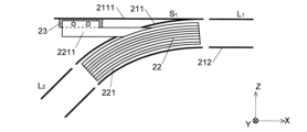
イオン飛行部20は、主電極21と、補償電極22と、補償電極取付具23とを有する。
The
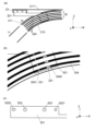
主電極21は、回転楕円体状の外側電極211と、該外側電極211の内側に設けられた略回転楕円体状の内側電極212とを有する。図1(a)では、外側電極211及び内側電極212の略回転楕円体における回転軸であるZ軸と、該Z軸に垂直な1方向の軸であるX軸を含む平面であるZX平面での断面図(縦断面図)を示している。主電極21は、Z軸を含む面で切断すると、断面の方位角(Z軸の周りの角度)に依らず、図1(a)に示したものと略同一の形状を呈する。図1(b)では、Z軸の正の方向から見た上面図を示している。Z軸及びX軸に垂直な軸をY軸とし、X軸とY軸を含む平面をXY平面とする。
The
外側電極211及び内側電極212は、ZX平面において曲線状である1対の電極を向かい合わせた3組の部分電極対S1、S2及びS3と、ZX平面において直線状である1対の電極を向かい合わせた4組の部分電極対L1, L2, L3及びL4とを組み合わせて成る。部分電極対S2は、ZX平面において、主電極21のX方向に関する両端に配置されており、X軸に関して線対称の形状を有する。部分電極対S1は、部分電極対S2よりもZ方向の正の側に配置されている。部分電極対S3は、部分電極対S2よりもZ方向の負の側に、X軸に関して部分電極対S1と線対称となるように配置されている。部分電極対L2は部分電極対S1とS2の間に配置されている。部分電極対L3は部分電極対S2とS3の間に配置され、X軸に関して部分電極対L2と線対称の形状を有する。部分電極対L1は、Z軸に垂直なドーナツ板状の形状を有し、Z方向の正の側であってXY平面において部分電極対S1の内側に配置されている。部分電極対L4は、Z方向の負の側に、X軸に関して部分電極対L1と線対称となるように配置されている。
The
これらの部分電極対の組み合わせにより、外側電極211及び内側電極212はそれぞれ、全体で略回転楕円体の形状を呈している。外側電極211の外形は、例えば、長軸方向(X方向、Y方向)が500mm、短軸方向(Z方向)が300mmである。外側電極211と内側電極212の間隔は20mmである。外側電極211及び内側電極212の全体を小さくすることにより、MT-TOFMS1の全体を小型化することができる。
By combining these partial electrode pairs, each of the
ZX平面において曲線状である部分電極対S1、S2及びS3には、図示せぬ電源によって、外側電極211から内側電極212に向かう電場が形成されるように電位が付与される。一方、ZX平面において直線状である部分電極対L1, L2, L3及びL4には、図示せぬ電源によって、外側電極211と内側電極212に同じ電位が付与される。これにより、外側電極211と内側電極212の間の空間に、該空間内でイオンを周回させる周回電場が形成される。この空間を周回空間219と呼ぶ。
A potential is applied to the curved partial electrode pairs S 1 , S 2 and S 3 in the ZX plane by a power source (not shown) so that an electric field is formed from the
外側電極211のうち部分電極対S1には、イオン源11から出射されるイオンを周回空間219内に導入するイオン導入口24が設けられている。イオン導入口24は、X軸からわずかにY方向の正の側にずれた位置に設けられており、イオン源11からイオンがX軸に略平行に入射するように配置されている。イオンは、イオン導入口24から周回空間219に入射した直後の位置において、部分電極対S1による周回電場から向心力を受けると共に、イオン導入口24がX軸からY方向の正の側にずれていることにより、X軸方向に向かう力を受ける。これにより、イオンは、周回空間219を略楕円形の周回軌道に沿って周回し、1周する毎に、周回軌道がY方向の正の側から見て反時計回りに移動するような軌道218(図2参照)で飛行する。図2では、イオンの軌道218をXY平面の上面図で示している。
The partial electrode pair S 1 of the
また、部分電極対S3には、周回空間219内を複数回(数十回)周回したイオンを周回空間219から導出するイオン導出口25が設けられている。イオン導出口25から導出されるイオンは直線状の軌道を飛行する。この直線状の軌道上にイオン検出器12が配置されている。
Further, the partial electrode pair S 3 is provided with an ion lead-out
これらイオン源11、主電極21及びイオン検出器12の構成により、イオン源11から出射された、種々の質量電荷比を有する多数のイオンは、主電極21内の周回空間219を飛行し、各イオンの質量電荷比に対応した時間差をもってイオン検出器12で検出されることで質量分離がなされる。しかし、イオンが周回空間219に導入された直後に通過するイオン導入口24付近の位置では、外側電極211にイオン導入口24として開口が設けられていることにより歪電場が生じ、そのままではイオンの軌道が本来の位置からずれてしまい、イオン導出口25からイオンを導出することができなくなるおそれがある。そこで、本実施形態のMT-TOFMS1には補償電極22が設けられている。
Due to the configuration of the
補償電極22は、図1(a)及びその部分拡大図である図4に示すように、周回空間219中の部分電極対S1で挟まれた部分であって、XY面(図1(b))では、イオン導入口24からY方向の負の側に、イオン導入口24から導入されたイオンが1周した後の周回軌道の位置よりも近く、該軌道に重ならないようにずれた位置に配置されている。イオン導入口24と補償電極22の距離は10mm未満であり、外側電極211と内側電極212の間隔である20mmよりも小さい。この補償電極22の位置は、補償電極22が無ければ(又は補償電極22が動作しなければ)イオン導入口24により生じる電場の歪みの影響を受ける範囲内にあり、前記「開口(イオン導入口24)の近傍」に該当する。図3(a)に、本実施形態のMT-TOFMS1から補償電極22を除いた構成において、イオン導入口24の近傍を飛行するイオンの軌跡をシミュレーションで求めた図を示す。この図に示すように、補償電極22が無い(動作していない)場合には、イオン導入口24から導入されたイオンの一部210は、イオンの軌道218が1周した位置付近において散乱されており、補償電極22が配置される位置において電場の歪みの影響を受けることがわかる。
As shown in FIG. 1(a) and its partial enlarged view in FIG. 4, the compensating
補償電極22は、ZX平面における部分電極対S1の曲線に沿った形状を有する線状導電体が、外側電極211から内側電極212に向かって複数本配置されたものである。補償電極22は、絶縁体(本実施形態ではアルミナ)から成る基板221の表面に取り付けられている。基板221の一部である基板突出部2211は、外側電極211に設けられた孔を通して主電極21の外に突出している。各線状導電体には図示せぬ電源が接続されており、これにより、外側電極211から内側電極212に向かう補償電場が形成される。この補償電場により、イオン導入口24である開口や基板221を通過させる孔が外側電極211に存在することによって主電極21で形成される歪電場が補償される。図3(b)に、本実施形態のMT-TOFMS1の補償電極22が動作している状態において、イオン導入口24の近傍を飛行するイオンの軌跡をシミュレーションで求めた図を示す。補償電極22が動作することにより、イオンの散乱が生じなくなり、歪電場が補償されていることがわかる。
The compensating
但し、仮に補償電極22が周回空間219内の正確な位置に配置されていなければ、補償電場が設計通りに形成されず、歪電場を補償することができなくなる。特に、イオンの飛行距離を短くすることなく(すなわち、分解能を低下させることなく)外側電極211及び内側電極212の全体を小さくしたり、イオンの飛行距離を長くすると、周回軌道の間隔が小さくなるため、イオン導入口24近傍の歪電場の影響をより受け易くなる。例えば、イオンの飛行距離を短くすることなく、外側電極211の長軸方向の外径を700mmから500mmに変更する(外側電極211と内側電極212の間隔はいずれも20mmとする)と、周回軌道の間隔が50mm程度から10mm以下になり、よりイオン導入口24に近い位置を通過することとなる。そのため、補償電極22の取り付け位置の精度は、外側電極211の長軸方向の外径が700mmであるときには500μm以下であれば十分であるのに対して、同外径が500mmであるときには100μm以下にする必要がある。そこで、本実施形態のMT-TOFMS1では、補償電極22がより正確な位置に配置されるように、補償電極取付具23を用いる。なお、補償電極取付具23は、補償電極22の取り付け位置の精度を100μm以下にする場合には限らず、それよりも同精度が低いことが許容される(例えば500μm以下である)場合に用いてもよい。
However, if the compensating
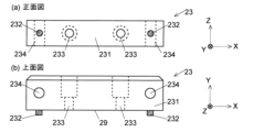
以下、補償電極取付具23が主電極21に取り付けられた状態における方向を基準として、補償電極取付具23の構成を説明する。補償電極取付具23は、図5に示すように、略直方体の絶縁体から成る本体231と、該本体231からY方向の負の側の面(この面を補償電極取付面29と呼ぶ)に突出して設けられた2個の円柱状の位置決めピン232と、Y方向に貫くように2個設けられた補償電極固定ボルト挿通孔233と、Z方向に貫くように2個設けられた主電極固定ボルト挿通孔234とを有する。
The configuration of the compensating
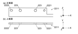
補償電極22の基板突出部2211は、その板面をZX平面に平行に向け、補償電極取付具23の本体231におけるY方向の負側の面に取り付けられる。基板突出部2211には、図6に示すように、補償電極取付具23の2個の位置決めピン232及び2個の補償電極固定ボルト挿通孔233の位置に対応して、2個の位置決めピン係合孔2221、2222及び補償電極固定ボルト取付孔223が設けられている。2個の位置決めピン係合孔のうちの一方である、より補償電極22に近い側に設けられた位置決めピン係合孔2221は、円柱状の位置決めピン232の外形と略同一である円形の平面形状を呈している。他方の位置決めピン係合孔2222は、Z方向には位置決めピン232と略同一の幅を有し、X方向には位置決めピン232よりも広い幅を有する長孔状の形状を呈している。
The
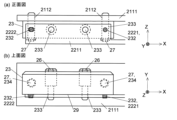
図4、図7に示すように、外側電極211のうち部分電極対S1に属する部分には、外方に突出する取付具固定部2111が設けられており、取付具固定部2111には補償電極取付具23の2個の主電極固定ボルト挿通孔234に対応する2個の主電極固定ボルト取付孔2112が設けられている。なお、図7(b)の上面図では、基板突出部2211及び補償電極取付具23は、取付具固定部2111の裏側(下側)に設けられているため本来は上面図には現れないが、説明の都合上、実線で示している。
As shown in FIGS. 4 and 7, a portion of the
図7に示すように、補償電極22の基板突出部2211を補償電極取付具23のY方向の負側の面に密着させ、2個の位置決めピン係合孔2221、2222にそれぞれ1個ずつ位置決めピン232を挿入し、補償電極固定ボルト26を2個の補償電極固定ボルト挿通孔233にそれぞれ挿通したうえで補償電極固定ボルト取付孔223に取り付けることにより、基板突出部2211は補償電極取付具23に固定されている。また、2個の主電極固定ボルト挿通孔234にそれぞれ主電極固定ボルト27を挿通させたうえで主電極固定ボルト取付孔2112に取り付けることにより、補償電極取付具23は、主電極21の外側電極211に設けられた取付具固定部2111に固定されている。こうして、補償電極22は補償電極取付具23を介して主電極21に固定されている。
As shown in FIG. 7, the
2個の位置決めピン232の位置及び円柱の径、一方の位置決めピン係合孔2221の位置及び径、並びに他方の位置決めピン係合孔2222の位置及びZ方向の幅は、補償電極固定ボルト取付孔223、補償電極固定ボルト挿通孔233よりも小さい公差(例えば10~30μm)で作製される。そのため、補償電極22のX方向の位置は一方の位置決めピン係合孔2221及びそれに挿入される位置決めピン232によって高精度(例えば上記公差が10~30μmである場合には100μm以下)に設定される。なお、本実施形態では、他方の位置決めピン係合孔2222を位置決めピン232よりもX方向に広い幅を有する長孔とすることにより、公差以内のわずかな誤差によって2個の位置決めピン232を位置決めピン係合孔2221、2222に挿入し難くなることを防止している。また、補償電極22のZ方向の位置は、2個の位置決めピン係合孔2221、2222及びそれに挿入される位置決めピン232によって高精度に設定される。一方、補償電極22のY方向の位置は、補償電極22の基板突出部2211を補償電極取付面29に密着させることにより、高精度に位置決めされる。
The position and diameter of the two
以上のように、本実施形態のMT-TOFMS1では、補償電極22が高精度に位置決めされるため、イオン導入口24の近傍に生じる歪電場を補償電場によってより高精度に補償することができる。これにより、主電極21を小型化するために、あるいは分解能を高くするために、イオンが1周する毎に生じる周回軌道の移動を小さくすることによって、1周後の軌道がイオン導入口24に近くなっても、歪電場による影響を抑えることができる。そのため、本実施形態ではMT-TOFMSを小型化すること、あるいは分解能を高くすることができる。
As described above, in the MT-
(2) 本実施形態のMT-TOFMSの第1変形例
次に、図8を参照しつつ、本実施形態のMT-TOFMSの第1変形例を説明する。第1変形例のMT-TOFMSは、補償電極32が上記実施形態のMT-TOFMS1における補償電極22とは異なる構成を有する。補償電極32以外の構成(主電極21、補償電極取付具23、イオン源11,イオン検出器12)は上記実施形態のものと同様である。
(2) First Modification of MT-TOFMS of this Embodiment Next, a first modification of the MT-TOFMS of this embodiment will be described with reference to FIG. In the MT-TOFMS of the first modified example, the compensating
補償電極32は、ZX平面における部分電極対S1の曲線に沿った曲線状の形状を有し、剛性を有する(前記形状を維持することができる)導電体324が複数本、外側電極211から内側電極212に向かって配置されたものである。各導電体324には2個ずつ、Y方向に向かって貫通する位置決めピン係合孔3421、3422が設けられている。一方の位置決めピン係合孔3421は円形であり、他方の位置決めピン係合孔3242は導電体324の曲線に沿って延びる長孔の形状を呈している。
The compensating
補償電極32は、絶縁体製の基板321に取り付けられている。基板321にはY方向の負側に延びる位置決めピン332(補償電極取付具23に設けられた位置決めピン232とは異なる)が、導電体324の本数の2倍の個数設けられている。各導電体324は、位置決めピン係合孔3241及び3242にそれぞれ位置決めピン332を1個ずつ挿入したうえで、ねじにより基板321に固定されている。基板321は、補償電極32の一部のみを支持しており、上記実施形態のMT-TOFMS1における基板221よりも面積が小さい。これにより、周回空間219内において絶縁体製である基板321に電荷が蓄積されること(チャージアップ)が抑制される。
The
基板321にはさらに、上記実施形態の基板221と同様に、2個の位置決めピン係合孔3221、3222及び補償電極固定ボルト取付孔323が設けられている(図8(c))。これら位置決めピン係合孔3221、3222にそれぞれ、補償電極取付具23に設けられた位置決めピン232が挿入されたうえで、2個の補償電極固定ボルト挿通孔233にそれぞれ挿通された補償電極固定ボルト26が補償電極固定ボルト取付孔323に取り付けられることにより、基板321が補償電極取付具23に固定される。また、上記実施形態のMT-TOFMS1と同様に、補償電極取付具23が主電極21に固定される。これにより、基板321に固定されている補償電極32は、周回空間219内の所定の位置に高い位置精度で固定される。
The
(3) 本実施形態のMT-TOFMSの第2変形例及びその製造方法
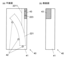
次に、図9を参照しつつ、本実施形態のMT-TOFMSの第2変形例及びその製造方法を説明する。第2変形例のMT-TOFMSは、上記実施形態のMT-TOFMS1において位置決めピン232及び位置決めピン係合孔2221、2222を省略した構成を有する(図示省略)。本変形例では、これら位置決めピン232及び位置決めピン係合孔2221、2222を用いる代わりに、以下に述べるようにMT-TOFMSを作製する際に図9に示す治具40を用いることにより、主電極21に対する補償電極22の位置決めを行う。
(3) Second Modified Example of MT-TOFMS of this Embodiment and Manufacturing Method Thereof Next, a second modified example of the MT-TOFMS of this embodiment and its manufacturing method will be described with reference to FIG. The MT-TOFMS of the second modification has a configuration in which the
治具40は、板状の本体41の1つの面(当該面を上面とする)に、3個の位置決めピン42と1つの凹部43を設けたものである。凹部43は、補償電極取付面29を上側に向けた補償電極取付具23と略同一の形状を有する。3個の位置決めピン42は、凹部43に補償電極取付面29を上側に向けて補償電極取付具23を配置した状態で、該補償電極取付具23に対する補償電極22の基板221が正確な位置に配置されている場合に、該基板221の縁に接触する位置に設けられている。3個の位置決めピン42のうちの2個は、補償電極22の曲線に沿って基板221に形成されている曲線状の縁に接触し、残りの1個は、曲線状の縁に交差する直線状の縁に接触する。
The
本変形例のMT-TOFMSでは、製造時に、凹部43に補償電極取付面29を上側に向けて補償電極取付具23を配置したうえで、基板221の縁が3個の位置決めピン42に接触するように該基板221を配置した状態で、2個の補償電極固定ボルト挿通孔233にそれぞれ挿通された補償電極固定ボルト26を補償電極固定ボルト取付孔223に取り付ることにより、基板221を補償電極取付具23に固定する。その後、基板221及び補償電極取付具23を治具40から取り出したうえで、外側電極211に設けられた孔に基板221の基板突出部2211を通し、補償電極取付具23を外側電極211の取付具固定部2111に固定する。これにより、基板221に設けられた補償電極22が正確に位置決めされる。
In the MT-TOFMS of this modified example, the compensating
(4) その他の変形例
本発明は、ここまでに述べた実施形態及び2つの変形例には限定されず、さらに種々の変形が可能である。
(4) Other Modifications The present invention is not limited to the embodiment and the two modifications described above, and various modifications are possible.
例えば、上記実施形態及び2つの変形例では補償電極22をイオン導入口24の近傍に配置しているが、イオン導出口25の近傍に同様の補償電極を配置してもよい。また、イオン導入口24の近傍には補償電極を配置せず、イオン導出口25の近傍にのみ補償電極を配置してもよい。
For example, although the
上記実施形態及び2つの変形例では補償電極22を、イオン導入口24から導入されたイオンが1周した後の周回軌道の位置よりも近い位置に配置しているが、イオン導入口24から外側電極211と内側電極212間の距離の範囲内となる20mm以下の範囲内に配置してもよい。また、イオン導入口24に由来する電場の歪みの影響が生じている範囲内であれば、イオン導入口24から外側電極211と内側電極212間の距離よりも離れた位置に補償電極22を配置してもよい。このような電場の歪みの影響が生じている範囲は、予備実験又はシミュレーションによって適宜求めることができる。イオン導出口25の近傍に補償電極を配置する場合も同様である。
In the above-described embodiment and two modifications, the
第1変形例では基板321に設けられた位置決めピン332を用いて補償電極32と基板321の間の位置決めを行うと共に、補償電極取付具23に設けられた位置決めピン232を用いて基板321と補償電極取付具23の間の位置決めを行っているが、位置決めピン232は用いずに、基板321と補償電極取付具23を一体化してもよい。この場合、基板321と補償電極取付具23が一体化したものの全体が補償電極取付具とみなされ、補償電極32が補償電極取付具に直接取り付けられることとなる。そして、位置決めピン332によって、補償電極32と補償電極取付具の位置決めがなされる。イオン導出口25の近傍に補償電極を配置する場合も同様である。
In the first modification, positioning pins 332 provided on the
[態様]
上述した例示的な実施形態及びその変形例が以下の態様の具体例であることは、当業者であれば容易に理解される。
[Aspect]
Those skilled in the art will readily understand that the exemplary embodiments described above and variations thereof are specific examples of the following aspects.
(第1項)
第1項に係るマルチターン型飛行時間型質量分析装置は、
イオンを複数回周回するように飛行させる電場である周回電場を所定の周回空間内に生成する電極であって、イオンを前記周回空間に導入又は前記周回空間から導出する開口を有する主電極と、
前記主電極に固定された、絶縁体製の補償電極取付具と、
前記補償電極取付具に直接又は基板を介して固定され、前記開口の近傍に配置された、前記開口の近傍に生じる前記周回電場の歪みを補償する補償電極と
を備える。
(Section 1)
The multi-turn time-of-flight mass spectrometer according to
A main electrode that generates an orbiting electric field, which is an electric field that causes ions to fly in a plurality of orbits, within a predetermined orbital space, the main electrode having an opening that introduces ions into or leads out of the orbital space;
a compensating electrode fixture made of insulator and fixed to the main electrode;
and a compensating electrode fixed to the compensating electrode fixture directly or via a substrate and arranged in the vicinity of the opening for compensating distortion of the circulating electric field generated in the vicinity of the opening.
第1項に係るマルチターン型飛行時間型質量分析装置によれば、補償電極が、絶縁体から成る補償電極取付具を介して主電極に固定されているため、主電極に対する補償電極の位置を従来よりも正確に設定することができる。そのため、主電極の開口の近傍に生じる歪電場を、補償電極が生成する補償電場によってより高精度に補償することができ、装置を小型化することや分解能を高くすることができる。
According to the multi-turn time-of-flight mass spectrometer according to
(第2項)
第2項に係るマルチターン型飛行時間型質量分析装置は、第1項に係るマルチターン型飛行時間型質量分析装置において、
前記補償電極取付具は2個の位置決めピンを有し、
前記補償電極又は前記基板は前記2個の位置決めピンに対応して1個ずつ設けられた係合孔を有する。
(Section 2)
The multi-turn time-of-flight mass spectrometer according to paragraph 2 is the multi-turn time-of-flight mass spectrometer according to
The compensation electrode fixture has two positioning pins,
The compensating electrode or the substrate has engaging holes provided one by one corresponding to the two positioning pins.
第2項に係るマルチターン型飛行時間型質量分析装置によれば、補償電極取付具に対する補償電極の位置をより正確に設定することができ、歪電場をより高精度に補償することができる。 According to the multi-turn time-of-flight mass spectrometer according to item 2, the position of the compensation electrode with respect to the compensation electrode fixture can be set more accurately, and the distorted electric field can be compensated for with higher accuracy.
(第3項)
第3項に係るマルチターン型飛行時間型質量分析装置は、第2項に係るマルチターン型飛行時間型質量分析装置において、前記係合孔のうちの1つが、一方向に関して、前記2個の位置決めピンのうち該係合孔に係合される位置決めピンよりも長い形状を有する。
(Section 3)
The multi-turn time-of-flight mass spectrometer according to item 3 is the multi-turn time-of-flight mass spectrometer according to item 2, wherein one of the engagement holes is one of the two engagement holes in one direction. Among the positioning pins, the positioning pin has a longer shape than the positioning pin engaged with the engagement hole.
第3項に係るマルチターン型飛行時間型質量分析装置によれば、公差以内のわずかな誤差によって2個の位置決めピンを係合孔に挿入し難くなることを防止することができる。 According to the multi-turn time-of-flight mass spectrometer according to item 3, it is possible to prevent difficulty in inserting the two positioning pins into the engagement holes due to a slight error within the tolerance.
(第4項)
第4項に係るマルチターン型飛行時間型質量分析装置は、第1~3項のいずれか1項に係るマルチターン型飛行時間型質量分析装置において、前記基板が前記補償電極の一部のみを支持している。
(Section 4)
The multi-turn time-of-flight mass spectrometer according to
第4項に係るマルチターン型飛行時間型質量分析装置によれば、基板を小型化することができ、基板に電荷が蓄積されること(チャージアップ)が抑制される。
According to the multi-turn time-of-flight mass spectrometer according to
(第5項)
第5項に係るマルチターン型飛行時間型質量分析装置は、第1~4項のいずれか1項に係るマルチターン型飛行時間型質量分析装置において、
前記主電極が、前記開口が設けられた外側電極と該外側電極よりも所定距離だけ内側に設けられた内側電極により構成されており、
前記周回空間が前記外側電極と前記内側電極の間の空間であって、
前記補償電極取付具が、前記開口から前記所定距離の範囲内に設けられている。
(Section 5)
The multi-turn time-of-flight mass spectrometer according to paragraph 5 is the multi-turn time-of-flight mass spectrometer according to any one of
The main electrode is composed of an outer electrode provided with the opening and an inner electrode provided inside the outer electrode by a predetermined distance,
wherein the winding space is a space between the outer electrode and the inner electrode,
The compensating electrode fixture is provided within the predetermined distance from the opening.
第5項に係るマルチターン型飛行時間型質量分析装置によれば、開口が存在することによって生じる電場の歪みが周回イオン軌道に与える影響が大きい範囲内に補償電極を配置することができ、電場の歪みの影響を効果的に低減することができる。 According to the multi-turn time-of-flight mass spectrometer according to item 5, the compensating electrode can be arranged in a range where the distortion of the electric field caused by the presence of the aperture has a large effect on the orbiting ion trajectory, and the electric field can effectively reduce the effect of the distortion of
(第6項)
第6項に係るマルチターン型飛行時間型質量分析装置の製造方法は、イオンを複数回周回するように飛行させる電場である周回電場を所定の周回空間内に生成する電極であって、イオンを前記周回空間に導入又は前記周回空間から導出する開口を有する主電極と、前記開口の近傍に配置された、前記開口の近傍に生じる前記周回電場の歪みを補償する補償電極とを有するマルチターン型飛行時間型質量分析装置を製造する方法であって、
前記補償電極を保持する補償電極保持部と、絶縁体製の補償電極取付具を該補償電極に対して所定の位置に保持する補償電極取付具保持部とを有する治具を用い、該補償電極保持部に該補償電極を保持すると共に該補償電極取付具保持部に該補償電極取付具を保持した状態で、該補償電極又は該補償電極が取り付けられた基板を該補償電極取付具に固定する工程と、
前記補償電極取付具を前記主電極の、前記開口の近傍に固定する工程と
を有する。
(Section 6)
In the method for manufacturing a multi-turn time-of-flight mass spectrometer according to item 6, an electrode for generating a circulating electric field, which is an electric field for causing ions to circulate a plurality of times, in a predetermined circulating space, A multi-turn type having a main electrode having an opening leading into or out of the circulating space, and a compensating electrode disposed near the opening for compensating distortion of the circulating electric field generated near the opening. A method of manufacturing a time-of-flight mass spectrometer, comprising:
Using a jig having a compensating electrode holding part for holding the compensating electrode and a compensating electrode fixture holding part for holding a compensating electrode fixture made of an insulating material at a predetermined position with respect to the compensating electrode, the compensating electrode is With the compensation electrode held by the holding part and the compensation electrode fixture held by the compensation electrode fixture holding part, the compensation electrode or the substrate to which the compensation electrode is attached is fixed to the compensation electrode fixture. process and
and securing the compensation electrode fixture to the main electrode proximate the opening.
第6項に係るマルチターン型飛行時間型質量分析装置の製造方法によれば、補償電極保持部に補償電極を保持すると共に補償電極取付具保持部に補償電極取付具を保持した状態で、補償電極又は該補償電極が取り付けられた基板を補償電極取付具に固定することにより、補償電極取付具に対する補償電極又は基板の位置をより正確に設定することができ、歪電場をより高精度に補償することができる。 According to the method for manufacturing a multi-turn time-of-flight mass spectrometer according to the sixth aspect, in a state in which the compensation electrode is held by the compensation electrode holding part and the compensation electrode fixture is held by the compensation electrode fixture holding part, By fixing the electrode or the substrate to which the compensation electrode is attached to the compensation electrode fixture, the position of the compensation electrode or the substrate with respect to the compensation electrode fixture can be set more accurately, and the distorted electric field can be compensated with higher accuracy. can do.
1…TOFMS
11…イオン源
12…イオン検出器
20…イオン飛行部
21…主電極
211…外側電極
2111…取付具固定部
2112…主電極固定ボルト取付孔
212…内側電極
218…イオンの軌道
219…周回空間
210…イオン導入口から導入されたイオンの一部
22、32…補償電極
221、321…基板
2211…基板突出部
2221、2222、3221、3222、3241、3242…位置決めピン係合孔
223、323…補償電極固定ボルト取付孔
23…補償電極取付具
231…補償電極取付具の本体
232、332…位置決めピン
233…補償電極固定ボルト挿通孔
234…主電極固定ボルト挿通孔
24…イオン導入口
25…イオン導出口
26…補償電極固定ボルト
27…主電極固定ボルト
29…補償電極取付面
324…導電体
40…治具
41…治具の本体
42…治具に設けられた位置決めピン
43…凹部
1 TOFMS
REFERENCE SIGNS LIST 11: Ion source 12: Ion detector 20: Ion flight part 21: Main electrode 211: Outer electrode 2111: Mounting fixture fixing part 2112: Main electrode fixing bolt mounting hole 212: Inner electrode 218: Ion trajectory 219: Orbital space 210 Part of the ions introduced from the
Claims (7)
前記主電極に固定された、絶縁体製の補償電極取付具と、
前記補償電極取付具に直接又は基板を介して固定され、前記開口の近傍に配置された、前記開口の近傍に生じる前記周回電場の歪みを補償する補償電極と
を備えるマルチターン型飛行時間型質量分析装置。 A circulating electric field is generated in a predetermined circulating space, which is an electric field that causes the ions to repeatedly circulate in a trajectory of a predetermined shape and to cause the ions to fly so that the trajectory rotates around a predetermined rotation axis for each trajectory. a main electrode having an opening for introducing ions into or out of the orbiting space;
a compensating electrode fixture made of insulator and fixed to the main electrode;
a compensation electrode that is fixed to the compensation electrode fixture directly or via a substrate and positioned near the opening for compensating distortion of the circulating electric field that occurs near the opening. Analysis equipment.
前記補償電極又は前記基板は前記2個の位置決めピンに対応して1個ずつ設けられた係合孔を有する、
請求項1又は2に記載のマルチターン型飛行時間型質量分析装置。 The compensation electrode fixture has two positioning pins,
The compensation electrode or the substrate has engagement holes provided one each corresponding to the two positioning pins,
The multi-turn time-of-flight mass spectrometer according to claim 1 or 2 .
前記周回空間が前記外側電極と前記内側電極の間の空間であって、
前記補償電極取付具が、前記開口から前記所定距離の範囲内に設けられている、
請求項1~5のいずれか1項に記載のマルチターン型飛行時間型質量分析装置。 The main electrode is composed of an outer electrode provided with the opening and an inner electrode provided inside the outer electrode by a predetermined distance,
wherein the winding space is a space between the outer electrode and the inner electrode,
wherein the compensating electrode fixture is provided within the predetermined distance from the opening;
A multi-turn time-of-flight mass spectrometer according to any one of claims 1 to 5 .
前記補償電極を保持する補償電極保持部と、絶縁体製の補償電極取付具を該補償電極に対して所定の位置に保持する補償電極取付具保持部とを有する治具を用い、該補償電極保持部に該補償電極を保持すると共に該補償電極取付具保持部に該補償電極取付具を保持した状態で、該補償電極又は該補償電極が取り付けられた基板を該補償電極取付具に固定する工程と、
前記補償電極取付具を前記主電極の、前記開口の近傍に固定する工程と
を有するマルチターン型飛行時間型質量分析装置の製造方法。 A main electrode that generates an orbiting electric field, which is an electric field that causes ions to fly in a plurality of orbits, within a predetermined orbital space, the main electrode having an opening that introduces ions into or leads out of the orbital space; and a compensating electrode arranged near the opening for compensating distortion of the circulating electric field generated near the opening, comprising:
Using a jig having a compensating electrode holding part for holding the compensating electrode and a compensating electrode fixture holding part for holding a compensating electrode fixture made of an insulating material at a predetermined position with respect to the compensating electrode, the compensating electrode is With the compensation electrode held by the holding part and the compensation electrode fixture held by the compensation electrode fixture holding part, the compensation electrode or the substrate to which the compensation electrode is attached is fixed to the compensation electrode fixture. process and
and fixing the compensating electrode fixture to the main electrode in the vicinity of the opening.
Priority Applications (3)
| Application Number | Priority Date | Filing Date | Title |
|---|---|---|---|
| JP2019187364A JP7322650B2 (en) | 2019-10-11 | 2019-10-11 | Multi-turn time-of-flight mass spectrometer and manufacturing method thereof |
| CN202010985178.1A CN112652516B (en) | 2019-10-11 | 2020-09-18 | Multi-transformation time-of-flight mass spectrometry device and manufacturing method thereof |
| US17/060,692 US11094522B2 (en) | 2019-10-11 | 2020-10-01 | Multiturn time-of-flight mass spectrometer and method for producing the same |
Applications Claiming Priority (1)
| Application Number | Priority Date | Filing Date | Title |
|---|---|---|---|
| JP2019187364A JP7322650B2 (en) | 2019-10-11 | 2019-10-11 | Multi-turn time-of-flight mass spectrometer and manufacturing method thereof |
Publications (2)
| Publication Number | Publication Date |
|---|---|
| JP2021064474A JP2021064474A (en) | 2021-04-22 |
| JP7322650B2 true JP7322650B2 (en) | 2023-08-08 |
Family
ID=75346404
Family Applications (1)
| Application Number | Title | Priority Date | Filing Date |
|---|---|---|---|
| JP2019187364A Active JP7322650B2 (en) | 2019-10-11 | 2019-10-11 | Multi-turn time-of-flight mass spectrometer and manufacturing method thereof |
Country Status (3)
| Country | Link |
|---|---|
| US (1) | US11094522B2 (en) |
| JP (1) | JP7322650B2 (en) |
| CN (1) | CN112652516B (en) |
Families Citing this family (2)
| Publication number | Priority date | Publication date | Assignee | Title |
|---|---|---|---|---|
| JP7311038B2 (en) * | 2020-04-24 | 2023-07-19 | 株式会社島津製作所 | ion analyzer |
| JP7548134B2 (en) * | 2021-06-16 | 2024-09-10 | 株式会社島津製作所 | Mass Spectrometer |
Citations (3)
| Publication number | Priority date | Publication date | Assignee | Title |
|---|---|---|---|---|
| JP2004014251A (en) | 2002-06-06 | 2004-01-15 | Jeol Ltd | Charged particle beam equipment |
| WO2008139506A1 (en) | 2007-05-09 | 2008-11-20 | Shimadzu Corporation | Charged particle analyzer |
| JP2014002914A (en) | 2012-06-18 | 2014-01-09 | Sharp Corp | Luminaire and display device |
Family Cites Families (15)
| Publication number | Priority date | Publication date | Assignee | Title |
|---|---|---|---|---|
| JPS5830696B2 (en) * | 1976-06-28 | 1983-06-30 | 株式会社日立製作所 | charged particle energy analyzer |
| JP2004362902A (en) * | 2003-06-04 | 2004-12-24 | Jeol Ltd | Time-of-flight mass spectrometer |
| US7351965B2 (en) * | 2006-01-30 | 2008-04-01 | Varian, Inc. | Rotating excitation field in linear ion processing apparatus |
| US20070278398A1 (en) * | 2006-05-30 | 2007-12-06 | Gangqiang Li | Ion mobility spectrometry waveform |
| WO2010038260A1 (en) * | 2008-10-02 | 2010-04-08 | 株式会社島津製作所 | Multi-turn time-of-flight mass spectrometer |
| JP4957848B2 (en) | 2008-10-09 | 2012-06-20 | 株式会社島津製作所 | Mass spectrometer |
| US8431887B2 (en) * | 2009-03-31 | 2013-04-30 | Agilent Technologies, Inc. | Central lens for cylindrical geometry time-of-flight mass spectrometer |
| JP5585394B2 (en) | 2010-11-05 | 2014-09-10 | 株式会社島津製作所 | Multi-turn time-of-flight mass spectrometer |
| CN103380479B (en) * | 2010-12-20 | 2016-01-20 | 株式会社岛津制作所 | Time-of-flight type quality analysis apparatus |
| GB201118279D0 (en) | 2011-10-21 | 2011-12-07 | Shimadzu Corp | Mass analyser, mass spectrometer and associated methods |
| GB201201403D0 (en) * | 2012-01-27 | 2012-03-14 | Thermo Fisher Scient Bremen | Multi-reflection mass spectrometer |
| US8766174B1 (en) * | 2013-02-14 | 2014-07-01 | Bruker Daltonik Gmbh | Correction of asymmetric electric fields in ion cyclotron resonance cells |
| JP6624482B2 (en) * | 2014-07-29 | 2019-12-25 | 俊 保坂 | Micro accelerator and micro mass spectrometer |
| GB2555609B (en) * | 2016-11-04 | 2019-06-12 | Thermo Fisher Scient Bremen Gmbh | Multi-reflection mass spectrometer with deceleration stage |
| WO2019014330A1 (en) * | 2017-07-11 | 2019-01-17 | Sterling Eduardo Mcbride | Compact electrostatic ion pump |
-
2019
- 2019-10-11 JP JP2019187364A patent/JP7322650B2/en active Active
-
2020
- 2020-09-18 CN CN202010985178.1A patent/CN112652516B/en active Active
- 2020-10-01 US US17/060,692 patent/US11094522B2/en active Active
Patent Citations (3)
| Publication number | Priority date | Publication date | Assignee | Title |
|---|---|---|---|---|
| JP2004014251A (en) | 2002-06-06 | 2004-01-15 | Jeol Ltd | Charged particle beam equipment |
| WO2008139506A1 (en) | 2007-05-09 | 2008-11-20 | Shimadzu Corporation | Charged particle analyzer |
| JP2014002914A (en) | 2012-06-18 | 2014-01-09 | Sharp Corp | Luminaire and display device |
Also Published As
| Publication number | Publication date |
|---|---|
| US20210111015A1 (en) | 2021-04-15 |
| US11094522B2 (en) | 2021-08-17 |
| JP2021064474A (en) | 2021-04-22 |
| CN112652516A (en) | 2021-04-13 |
| CN112652516B (en) | 2025-04-25 |
Similar Documents
| Publication | Publication Date | Title |
|---|---|---|
| US8431887B2 (en) | Central lens for cylindrical geometry time-of-flight mass spectrometer | |
| US9536722B2 (en) | Ion guide | |
| JP6323571B2 (en) | Mass spectrometer | |
| CN104011832B (en) | Mass-synchrometer, mass spectrograph and correlation technique | |
| US20160148796A1 (en) | Constraining arcuate divergence in an ion mirror mass analyser | |
| US20090206250A1 (en) | Parallel plate electrode arrangement apparatus and method | |
| US8618473B2 (en) | Mass spectrometer with precisely aligned ion optic assemblies | |
| US7919748B2 (en) | Cylindrical geometry time-of-flight mass spectrometer | |
| US6717133B2 (en) | Grating pattern and arrangement for mass spectrometers | |
| US9524857B2 (en) | Ion optics components and method of making the same | |
| JP7322650B2 (en) | Multi-turn time-of-flight mass spectrometer and manufacturing method thereof | |
| JP2006228435A (en) | Time-of-flight mass spectrometer | |
| US20060097147A1 (en) | Ion optics for mass spectrometers | |
| JP3395458B2 (en) | MS / MS quadrupole mass spectrometer | |
| EP2822021B1 (en) | Reduction of cross-talk between RF components in a mass spectrometer | |
| US11848185B2 (en) | Electrode assembly for mass spectrometer | |
| JP7556333B2 (en) | Time-of-flight mass spectrometer | |
| CN108811293B (en) | Charged particle accelerating field generation device | |
| US11587780B2 (en) | Time-of-flight mass spectrometer | |
| EP4020523B1 (en) | Manufacturing method for an ion guide | |
| RU2431213C2 (en) | Device for directing ion beam, having electrodes on parallel plates | |
| KR20110071320A (en) | Ion implanter, mass spectrometer including the same and ion focusing method using same | |
| JPS6276249A (en) | Charged particle energy analyzer |
Legal Events
| Date | Code | Title | Description |
|---|---|---|---|
| A621 | Written request for application examination |
Free format text: JAPANESE INTERMEDIATE CODE: A621 Effective date: 20220131 |
|
| A977 | Report on retrieval |
Free format text: JAPANESE INTERMEDIATE CODE: A971007 Effective date: 20221012 |
|
| A131 | Notification of reasons for refusal |
Free format text: JAPANESE INTERMEDIATE CODE: A131 Effective date: 20221122 |
|
| A601 | Written request for extension of time |
Free format text: JAPANESE INTERMEDIATE CODE: A601 Effective date: 20230120 |
|
| A521 | Request for written amendment filed |
Free format text: JAPANESE INTERMEDIATE CODE: A523 Effective date: 20230314 |
|
| TRDD | Decision of grant or rejection written | ||
| A01 | Written decision to grant a patent or to grant a registration (utility model) |
Free format text: JAPANESE INTERMEDIATE CODE: A01 Effective date: 20230627 |
|
| A61 | First payment of annual fees (during grant procedure) |
Free format text: JAPANESE INTERMEDIATE CODE: A61 Effective date: 20230710 |
|
| R151 | Written notification of patent or utility model registration |
Ref document number: 7322650 Country of ref document: JP Free format text: JAPANESE INTERMEDIATE CODE: R151 |