JP7319594B2 - connector device - Google Patents
connector device Download PDFInfo
- Publication number
- JP7319594B2 JP7319594B2 JP2020039412A JP2020039412A JP7319594B2 JP 7319594 B2 JP7319594 B2 JP 7319594B2 JP 2020039412 A JP2020039412 A JP 2020039412A JP 2020039412 A JP2020039412 A JP 2020039412A JP 7319594 B2 JP7319594 B2 JP 7319594B2
- Authority
- JP
- Japan
- Prior art keywords
- housing
- resin portion
- mold resin
- connector device
- protrusion
- Prior art date
- Legal status (The legal status is an assumption and is not a legal conclusion. Google has not performed a legal analysis and makes no representation as to the accuracy of the status listed.)
- Active
Links
Images


Classifications
-
- H—ELECTRICITY
- H01—ELECTRIC ELEMENTS
- H01R—ELECTRICALLY-CONDUCTIVE CONNECTIONS; STRUCTURAL ASSOCIATIONS OF A PLURALITY OF MUTUALLY-INSULATED ELECTRICAL CONNECTING ELEMENTS; COUPLING DEVICES; CURRENT COLLECTORS
- H01R43/00—Apparatus or processes specially adapted for manufacturing, assembling, maintaining, or repairing of line connectors or current collectors or for joining electric conductors
- H01R43/20—Apparatus or processes specially adapted for manufacturing, assembling, maintaining, or repairing of line connectors or current collectors or for joining electric conductors for assembling or disassembling contact members with insulating base, case or sleeve
- H01R43/24—Assembling by moulding on contact members
-
- H—ELECTRICITY
- H01—ELECTRIC ELEMENTS
- H01R—ELECTRICALLY-CONDUCTIVE CONNECTIONS; STRUCTURAL ASSOCIATIONS OF A PLURALITY OF MUTUALLY-INSULATED ELECTRICAL CONNECTING ELEMENTS; COUPLING DEVICES; CURRENT COLLECTORS
- H01R13/00—Details of coupling devices of the kinds covered by groups H01R12/70 or H01R24/00 - H01R33/00
- H01R13/46—Bases; Cases
- H01R13/502—Bases; Cases composed of different pieces
- H01R13/504—Bases; Cases composed of different pieces different pieces being moulded, cemented, welded, e.g. ultrasonic, or swaged together
-
- B—PERFORMING OPERATIONS; TRANSPORTING
- B23—MACHINE TOOLS; METAL-WORKING NOT OTHERWISE PROVIDED FOR
- B23K—SOLDERING OR UNSOLDERING; WELDING; CLADDING OR PLATING BY SOLDERING OR WELDING; CUTTING BY APPLYING HEAT LOCALLY, e.g. FLAME CUTTING; WORKING BY LASER BEAM
- B23K26/00—Working by laser beam, e.g. welding, cutting or boring
- B23K26/50—Working by transmitting the laser beam through or within the workpiece
- B23K26/57—Working by transmitting the laser beam through or within the workpiece the laser beam entering a face of the workpiece from which it is transmitted through the workpiece material to work on a different workpiece face, e.g. for effecting removal, fusion splicing, modifying or reforming
-
- B—PERFORMING OPERATIONS; TRANSPORTING
- B29—WORKING OF PLASTICS; WORKING OF SUBSTANCES IN A PLASTIC STATE IN GENERAL
- B29C—SHAPING OR JOINING OF PLASTICS; SHAPING OF MATERIAL IN A PLASTIC STATE, NOT OTHERWISE PROVIDED FOR; AFTER-TREATMENT OF THE SHAPED PRODUCTS, e.g. REPAIRING
- B29C65/00—Joining or sealing of preformed parts, e.g. welding of plastics materials; Apparatus therefor
- B29C65/02—Joining or sealing of preformed parts, e.g. welding of plastics materials; Apparatus therefor by heating, with or without pressure
- B29C65/14—Joining or sealing of preformed parts, e.g. welding of plastics materials; Apparatus therefor by heating, with or without pressure using wave energy, i.e. electromagnetic radiation, or particle radiation
- B29C65/16—Laser beams
-
- H—ELECTRICITY
- H01—ELECTRIC ELEMENTS
- H01R—ELECTRICALLY-CONDUCTIVE CONNECTIONS; STRUCTURAL ASSOCIATIONS OF A PLURALITY OF MUTUALLY-INSULATED ELECTRICAL CONNECTING ELEMENTS; COUPLING DEVICES; CURRENT COLLECTORS
- H01R12/00—Structural associations of a plurality of mutually-insulated electrical connecting elements, specially adapted for printed circuits, e.g. printed circuit boards [PCB], flat or ribbon cables, or like generally planar structures, e.g. terminal strips, terminal blocks; Coupling devices specially adapted for printed circuits, flat or ribbon cables, or like generally planar structures; Terminals specially adapted for contact with, or insertion into, printed circuits, flat or ribbon cables, or like generally planar structures
- H01R12/70—Coupling devices
- H01R12/7005—Guiding, mounting, polarizing or locking means; Extractors
- H01R12/7011—Locking or fixing a connector to a PCB
- H01R12/707—Soldering or welding
-
- H—ELECTRICITY
- H01—ELECTRIC ELEMENTS
- H01R—ELECTRICALLY-CONDUCTIVE CONNECTIONS; STRUCTURAL ASSOCIATIONS OF A PLURALITY OF MUTUALLY-INSULATED ELECTRICAL CONNECTING ELEMENTS; COUPLING DEVICES; CURRENT COLLECTORS
- H01R12/00—Structural associations of a plurality of mutually-insulated electrical connecting elements, specially adapted for printed circuits, e.g. printed circuit boards [PCB], flat or ribbon cables, or like generally planar structures, e.g. terminal strips, terminal blocks; Coupling devices specially adapted for printed circuits, flat or ribbon cables, or like generally planar structures; Terminals specially adapted for contact with, or insertion into, printed circuits, flat or ribbon cables, or like generally planar structures
- H01R12/70—Coupling devices
- H01R12/71—Coupling devices for rigid printing circuits or like structures
- H01R12/72—Coupling devices for rigid printing circuits or like structures coupling with the edge of the rigid printed circuits or like structures
- H01R12/722—Coupling devices for rigid printing circuits or like structures coupling with the edge of the rigid printed circuits or like structures coupling devices mounted on the edge of the printed circuits
- H01R12/724—Coupling devices for rigid printing circuits or like structures coupling with the edge of the rigid printed circuits or like structures coupling devices mounted on the edge of the printed circuits containing contact members forming a right angle
-
- H—ELECTRICITY
- H01—ELECTRIC ELEMENTS
- H01R—ELECTRICALLY-CONDUCTIVE CONNECTIONS; STRUCTURAL ASSOCIATIONS OF A PLURALITY OF MUTUALLY-INSULATED ELECTRICAL CONNECTING ELEMENTS; COUPLING DEVICES; CURRENT COLLECTORS
- H01R13/00—Details of coupling devices of the kinds covered by groups H01R12/70 or H01R24/00 - H01R33/00
- H01R13/40—Securing contact members in or to a base or case; Insulating of contact members
- H01R13/405—Securing in non-demountable manner, e.g. moulding, riveting
-
- H—ELECTRICITY
- H01—ELECTRIC ELEMENTS
- H01R—ELECTRICALLY-CONDUCTIVE CONNECTIONS; STRUCTURAL ASSOCIATIONS OF A PLURALITY OF MUTUALLY-INSULATED ELECTRICAL CONNECTING ELEMENTS; COUPLING DEVICES; CURRENT COLLECTORS
- H01R13/00—Details of coupling devices of the kinds covered by groups H01R12/70 or H01R24/00 - H01R33/00
- H01R13/46—Bases; Cases
- H01R13/52—Dustproof, splashproof, drip-proof, waterproof, or flameproof cases
- H01R13/5202—Sealing means between parts of housing or between housing part and a wall, e.g. sealing rings
-
- H—ELECTRICITY
- H01—ELECTRIC ELEMENTS
- H01R—ELECTRICALLY-CONDUCTIVE CONNECTIONS; STRUCTURAL ASSOCIATIONS OF A PLURALITY OF MUTUALLY-INSULATED ELECTRICAL CONNECTING ELEMENTS; COUPLING DEVICES; CURRENT COLLECTORS
- H01R43/00—Apparatus or processes specially adapted for manufacturing, assembling, maintaining, or repairing of line connectors or current collectors or for joining electric conductors
- H01R43/02—Apparatus or processes specially adapted for manufacturing, assembling, maintaining, or repairing of line connectors or current collectors or for joining electric conductors for soldered or welded connections
-
- H—ELECTRICITY
- H05—ELECTRIC TECHNIQUES NOT OTHERWISE PROVIDED FOR
- H05K—PRINTED CIRCUITS; CASINGS OR CONSTRUCTIONAL DETAILS OF ELECTRIC APPARATUS; MANUFACTURE OF ASSEMBLAGES OF ELECTRICAL COMPONENTS
- H05K2203/00—Indexing scheme relating to apparatus or processes for manufacturing printed circuits covered by H05K3/00
- H05K2203/13—Moulding and encapsulation; Deposition techniques; Protective layers
- H05K2203/1305—Moulding and encapsulation
- H05K2203/1316—Moulded encapsulation of mounted components
-
- H—ELECTRICITY
- H05—ELECTRIC TECHNIQUES NOT OTHERWISE PROVIDED FOR
- H05K—PRINTED CIRCUITS; CASINGS OR CONSTRUCTIONAL DETAILS OF ELECTRIC APPARATUS; MANUFACTURE OF ASSEMBLAGES OF ELECTRICAL COMPONENTS
- H05K3/00—Apparatus or processes for manufacturing printed circuits
- H05K3/22—Secondary treatment of printed circuits
- H05K3/28—Applying non-metallic protective coatings
- H05K3/284—Applying non-metallic protective coatings for encapsulating mounted components
Landscapes
- Engineering & Computer Science (AREA)
- Physics & Mathematics (AREA)
- Optics & Photonics (AREA)
- Manufacturing & Machinery (AREA)
- Mechanical Engineering (AREA)
- Plasma & Fusion (AREA)
- General Chemical & Material Sciences (AREA)
- Oil, Petroleum & Natural Gas (AREA)
- Chemical Kinetics & Catalysis (AREA)
- Chemical & Material Sciences (AREA)
- Health & Medical Sciences (AREA)
- Electromagnetism (AREA)
- Toxicology (AREA)
- Connector Housings Or Holding Contact Members (AREA)
- Laser Beam Processing (AREA)
- Manufacturing Of Electrical Connectors (AREA)
Description
本開示は、コネクタ装置に関する。 The present disclosure relates to connector devices.
特許文献1は、回路基板とコネクタの一部とが筐体に収納された電子装置を開示する。筐体は、ケースとカバーとを組み付けて構成される。シール材は、ケースとカバーとの間に介在され、筐体の内部空間を防水空間とする。以下、電子装置をコネクタ装置と呼ぶ。
上述のコネクタ装置は、筐体を備えることで大型である。また、上述のコネクタ装置は、筐体を構成するケースとカバーとの間にシール材を介在することで防水性能を確保しており、部品点数が多く、製造作業が煩雑になり易い。 The connector device described above is large due to the presence of the housing. In addition, the connector device described above secures waterproof performance by interposing a sealing material between the case and the cover that constitute the housing.
そこで、本開示は、小型で製造し易い上に、防水性能に優れるコネクタ装置を提供することを目的の一つとする。 Accordingly, one object of the present disclosure is to provide a connector device that is compact, easy to manufacture, and excellent in waterproof performance.
本開示に係るコネクタ装置は、
回路基板と、
コネクタと、
モールド樹脂部とを備え、
前記回路基板は、導体路を備え、
前記コネクタは、
樹脂で構成される筒状のハウジングと、
前記ハウジングの内側から前記ハウジングの軸方向外側に突出し、前記導体路に接続される端子とを備え、
前記モールド樹脂部は、前記回路基板と、前記ハウジングの外側に位置する前記端子と、前記ハウジングの一部とをまとめて覆い、
前記ハウジングは、前記モールド樹脂部に接触するように全周にわたって設けられる突起部を備え、
前記突起部は、前記ハウジングと前記モールド樹脂部の互いの構成材料が溶着されてなる溶着部を備える。
A connector device according to the present disclosure includes:
a circuit board;
a connector;
and a mold resin part,
The circuit board comprises a conductor track,
The connector is
a cylindrical housing made of resin;
a terminal projecting from the inside of the housing to the axial outside of the housing and connected to the conductor path,
The molded resin portion collectively covers the circuit board, the terminals positioned outside the housing, and a portion of the housing,
The housing has a protrusion provided over the entire circumference so as to contact the mold resin portion,
The projecting portion includes a welded portion formed by welding the constituent materials of the housing and the molded resin portion.
本開示に係るコネクタ装置は、小型で製造し易い上に、防水性能に優れる。 The connector device according to the present disclosure is compact, easy to manufacture, and excellent in waterproof performance.
[本開示の実施形態の説明]
最初に本開示の実施態様を列記して説明する。
[Description of Embodiments of the Present Disclosure]
First, the embodiments of the present disclosure are listed and described.
(1)本開示の一態様に係るコネクタ装置は、
回路基板と、
コネクタと、
モールド樹脂部とを備え、
前記回路基板は、導体路を備え、
前記コネクタは、
樹脂で構成される筒状のハウジングと、
前記ハウジングの内側から前記ハウジングの軸方向外側に突出し、前記導体路に接続される端子とを備え、
前記モールド樹脂部は、前記回路基板と、前記ハウジングの外側に位置する前記端子と、前記ハウジングの一部とをまとめて覆い、
前記ハウジングは、前記モールド樹脂部に接触するように全周にわたって設けられる突起部を備え、
前記突起部は、前記ハウジングと前記モールド樹脂部の互いの構成材料が溶着されてなる溶着部を備える。
(1) A connector device according to an aspect of the present disclosure includes:
a circuit board;
a connector;
and a mold resin part,
The circuit board comprises a conductor track,
The connector is
a cylindrical housing made of resin;
a terminal projecting from the inside of the housing to the axial outside of the housing and connected to the conductor path,
The molded resin portion collectively covers the circuit board, the terminals positioned outside the housing, and a portion of the housing,
The housing has a protrusion provided over the entire circumference so as to contact the mold resin portion,
The projecting portion includes a welded portion formed by welding the constituent materials of the housing and the molded resin portion.
本開示のコネクタ装置は、コネクタのハウジングの全周にわたって設けられる突起部に溶着部を備える。よって、本開示のコネクタ装置は、ハウジングの全周にわたって、ハウジングとモールド樹脂部との密着性に優れる。そのため、本開示のコネクタ装置は、ハウジングとモールド樹脂部との隙間から水等の液体が浸入することを抑制できる。液体の浸入を抑制できることで、モールド樹脂部で覆われる回路基板や端子等の導電部材に液体が付着することを抑制できる。 The connector device of the present disclosure includes a welded portion on a projection provided over the entire circumference of the housing of the connector. Therefore, the connector device of the present disclosure has excellent adhesion between the housing and the mold resin portion over the entire circumference of the housing. Therefore, the connector device of the present disclosure can prevent liquid such as water from entering through the gap between the housing and the mold resin portion. By suppressing the infiltration of the liquid, it is possible to suppress the liquid from adhering to the conductive members such as the circuit board and terminals covered with the molded resin portion.
溶着部は、代表的には、レーザー溶着により構成される。レーザー溶着では、モールド樹脂部を通してハウジングにレーザーを照射し、ハウジングとモールド樹脂部との境界面で熱を発生させることで、その熱によりハウジングとモールド樹脂部の互いの構成材料が溶着される。ここでは、モールド樹脂部はレーザーを透過し、ハウジングはレーザーを吸収する。レーザーを吸収したハウジングは発熱し、その発熱によってハウジングの構成材料が溶融する。ハウジングにおける溶融熱がモールド樹脂部に伝わることでモールド樹脂部が発熱し、その発熱によってモールド樹脂部が溶融する。溶融したハウジングの構成材料とモールド樹脂部の構成材料とで溶着部が構成される。 The welded portion is typically formed by laser welding. In laser welding, the housing is irradiated with a laser beam through the mold resin portion to generate heat at the interface between the housing and the mold resin portion. Here, the mold resin portion transmits the laser, and the housing absorbs the laser. The housing that absorbs the laser heats up, and the heat generated melts the constituent material of the housing. The heat of melting in the housing is transmitted to the mold resin portion, thereby generating heat in the mold resin portion, and the heat generation melts the mold resin portion. A welded portion is formed by the molten constituent material of the housing and the molten constituent material of the mold resin portion.
本開示のコネクタ装置は、突起部に溶着部を備える。つまり、本開示のコネクタ装置は、突起部でレーザーによる熱を発生させることで、溶着部が構成される。突起部で熱を発生させることで、その熱は突起部に集中し易く、強固な溶着部が構成され易い。以上より、本開示のコネクタ装置は、防水性能に優れる。 The connector device of the present disclosure includes a welding portion on the protrusion. In other words, in the connector device of the present disclosure, the welding portion is formed by generating heat from the laser at the projection. By generating heat at the protrusion, the heat tends to concentrate on the protrusion, and a strong welded portion is easily formed. As described above, the connector device of the present disclosure is excellent in waterproof performance.
本開示のコネクタ装置は、回路基板や端子等の導電部材をモールド樹脂部で覆っている。よって、本開示のコネクタ装置は、導電部材を収納する筐体を別途備える必要がない。また、本開示のコネクタ装置は、上述したように溶着部により防水性能に優れるため、シール材を別途備える必要がない。そのため、本開示のコネクタ装置は、部品点数が少なく、筐体を組み立てる作業やシール材を配置する作業を省略でき、製造性に優れる。以上より、本開示のコネクタ装置は、小型で製造し易い。 In the connector device of the present disclosure, conductive members such as a circuit board and terminals are covered with a molded resin portion. Therefore, the connector device of the present disclosure does not need to separately provide a housing for housing the conductive member. Moreover, since the connector device of the present disclosure is excellent in waterproof performance due to the welded portion as described above, it is not necessary to separately provide a sealing material. Therefore, the connector device of the present disclosure has a small number of parts, can omit the work of assembling the housing and the work of arranging the sealing material, and is excellent in manufacturability. As described above, the connector device of the present disclosure is small and easy to manufacture.
(2)本開示のコネクタ装置の一例として、
前記ハウジングは、前記モールド樹脂部に接触するように全周にわたって設けられると共に、その軸方向に並列される複数の凹部を備え、
前記突起部は、隣り合う前記凹部の側壁を構成する形態が挙げられる。
(2) As an example of the connector device of the present disclosure,
The housing is provided along the entire circumference so as to be in contact with the mold resin portion, and has a plurality of concave portions arranged in parallel in the axial direction thereof,
A form in which the protrusions constitute side walls of the adjacent recesses can be mentioned.
上記形態は、凹部にモールド樹脂部が充填される。そのため、凹部に充填されるモールド樹脂部がアンカーとなることに加え、突起部が一様な高さで凹部を備えない場合に比較して、ハウジングとモールド樹脂部との接触面積を大きくできる。よって、上記形態は、ハウジングとモールド樹脂部との密着性を向上し易い。 In the above configuration, the concave portion is filled with the mold resin portion. Therefore, the mold resin portion filled in the recess serves as an anchor, and the contact area between the housing and the mold resin portion can be increased compared to the case where the protrusions have a uniform height and no recess is provided. Therefore, the above-mentioned form tends to improve the adhesion between the housing and the mold resin portion.
また、上記形態は、凹部を設けることによって突起部を構成しているため、凹部がない場合に比較して、ハウジングの外表面から突出する突起部の突出量を小さくできる。よって、上記形態は、ハウジングの外表面からのモールド樹脂部の厚さを小さくし易く、小型化し易い。 Further, in the above embodiment, since the projection is formed by providing the recess, the amount of protrusion of the projection projecting from the outer surface of the housing can be reduced compared to the case where there is no recess. Therefore, in the above embodiment, it is easy to reduce the thickness of the molded resin portion from the outer surface of the housing, and to easily reduce the size.
(3)本開示のコネクタ装置の一例として、
前記突起部は、前記ハウジングの内側に位置する前記端子に対して交差するように設けられている形態が挙げられる。
(3) As an example of the connector device of the present disclosure,
The protrusion may be provided so as to intersect the terminal located inside the housing.
突起部は、ハウジングの全周にわたって設けられている。つまり、突起部は、環状に設けられている。上記形態では、環状の突起部よりも内周側に端子が挿通して配置されている。この形態の場合、ハウジングからの端子の突出箇所が突起部と近い。溶着部は、上述したように、熱によりハウジングとモールド樹脂部の互いの構成材料が溶着されて構成される。本開示のコネクタ装置は、突起部に溶着部を備えることで、熱を突起部に集中させることができる。そのため、ハウジングからの端子の突出箇所が突起部と近い場合であっても、熱が端子側に伝わることを抑制できる。よって、溶着部を構成する際に、端子、及び端子に接続される回路基板に悪影響が及ぶことを抑制できる。また、突起部に溶着部を備えることで、突起部を備えない場合に比較して、端子と溶着部との距離をある程度長く確保し易い。突起部を備えない場合、端子と溶着部との距離をある程度長く確保するには、端子を覆うハウジングの厚さを厚くすることが考えられる。しかし、この場合、ハウジングの構成材料が増える。 The protrusion is provided along the entire circumference of the housing. That is, the protrusion is provided in an annular shape. In the above embodiment, the terminal is inserted and arranged on the inner peripheral side of the annular protrusion. In this form, the projecting portion of the terminal from the housing is close to the projecting portion. As described above, the welding portion is formed by welding the constituent materials of the housing and the mold resin portion to each other by heat. The connector device of the present disclosure can concentrate heat on the protrusion by providing the protrusion with the welded portion. Therefore, even if the projecting portion of the terminal from the housing is close to the projecting portion, it is possible to suppress heat transfer to the terminal side. Therefore, it is possible to prevent the terminal and the circuit board connected to the terminal from being adversely affected when forming the welded portion. In addition, by providing the protrusion with the welded portion, it is easier to secure a somewhat longer distance between the terminal and the welded portion than in the case where the protrusion is not provided. In the case where the protrusion is not provided, it is conceivable to increase the thickness of the housing that covers the terminal in order to secure a certain long distance between the terminal and the welded portion. However, in this case, the constituent material of the housing increases.
(4)本開示のコネクタ装置の一例として、
前記突起部は、前記ハウジングの軸方向に平行な先端面を備える形態が挙げられる。
(4) As an example of the connector device of the present disclosure,
A form in which the projection has a tip end surface parallel to the axial direction of the housing may be mentioned.
溶着部は、上述したように、突起部でレーザーによる熱を発生させることで構成される。突起部が上記先端面を備えることで、突起部におけるレーザーを受ける面を安定して確保し易い。また、突起部が上記先端面を備えることで、熱が発生する領域を突起部の先端側に設け易く、熱が突起部の基端側に伝わることを抑制し易い。ここで、ハウジングの軸方向は、ハウジングの内側に位置する端子の長手方向である。 As described above, the welding portion is formed by generating heat with a laser at the protrusion. Since the projection has the tip surface, it is easy to stably secure the surface of the projection that receives the laser. In addition, since the projection has the distal end surface, it is easy to provide a region where heat is generated on the distal end side of the projection, and it is easy to suppress heat transfer to the proximal end side of the projection. Here, the axial direction of the housing is the longitudinal direction of the terminals located inside the housing.
(5)本開示のコネクタ装置の一例として、
前記突起部の横断面形状は、四角形である形態が挙げられる。
(5) As an example of the connector device of the present disclosure,
The lateral cross-sectional shape of the projection may be quadrangular.
モールド樹脂部は、ハウジングの外形に沿って構成される。しかし、ハウジングに複雑な形状の部位があると、モールド樹脂部は、その部位との間に隙間が形成され得る。上記形態は、突起部の形状が単純である。そのため、上記形態は、突起部とモールド樹脂部との密着性を向上し易い。また、上記形態は、突起部を製造し易い。 The molded resin portion is configured along the contour of the housing. However, if the housing has a part with a complicated shape, a gap may be formed between the mold resin part and that part. The above embodiment has a simple shape of the protrusion. Therefore, the above-mentioned form tends to improve the adhesion between the protrusion and the mold resin portion. Moreover, the said form is easy to manufacture a projection part.
(6)本開示のコネクタ装置の一例として、
前記突起部の最大幅は、1mm以上2mm未満である形態が挙げられる。
(6) As an example of the connector device of the present disclosure,
The maximum width of the protrusion may be 1 mm or more and less than 2 mm.
溶着部は、上述したように、突起部でレーザーによる熱を発生させることで構成される。突起部の最大幅が上記範囲を満たすことで、レーザーによる熱が突起部に集中し易い。 As described above, the welding portion is formed by generating heat with a laser at the protrusion. When the maximum width of the protrusion satisfies the above range, the heat generated by the laser tends to concentrate on the protrusion.
(7)本開示のコネクタ装置の一例として、
前記突起部の最大高さは、0.2mm以上0.5mm以下である形態が挙げられる。
(7) As an example of the connector device of the present disclosure,
The maximum height of the protrusion may be 0.2 mm or more and 0.5 mm or less.
溶着部は、上述したように、突起部でレーザーによる熱を発生させることで構成される。突起部の最大高さが上記範囲を満たすことで、レーザーによる熱の拡散が一定になり易く、突起部の溶融が一定になり易い。 As described above, the welding portion is formed by generating heat with a laser at the protrusion. When the maximum height of the protrusions satisfies the above range, the diffusion of heat by the laser tends to be uniform, and the melting of the protrusions tends to be uniform.
(8)本開示のコネクタ装置の一例として、
前記モールド樹脂部の透過率が40%以上である形態が挙げられる。
前記モールド樹脂部の透過率は、波長が940nmのレーザーの光量a1と、前記モールド樹脂部の構成材料からなる厚さ2mmの試験片を前記レーザーが透過した光量b1との比率(b1/a1)×100である。
(8) As an example of the connector device of the present disclosure,
A mode in which the transmittance of the mold resin portion is 40% or more is exemplified.
The transmittance of the mold resin portion is the ratio (b1/a1) of the light amount a1 of the laser having a wavelength of 940 nm and the light amount b1 of the laser transmitted through a test piece having a thickness of 2 mm made of the constituent material of the mold resin portion. x100.
溶着部は、上述したように、レーザー溶着により構成される。モールド樹脂部の透過率が40%以上であることで、レーザーは、モールド樹脂部で吸収され難く、ハウジングの表面まで到達し易い。そのため、上記形態は、ハウジングとモールド樹脂部との境界面でレーザーによる熱を発生させ易く、溶着部を構成し易い。 The welded portion is formed by laser welding as described above. Since the transmittance of the mold resin portion is 40% or more, the laser is less likely to be absorbed by the mold resin portion and easily reaches the surface of the housing. Therefore, in the above-described configuration, heat is easily generated by the laser at the interface between the housing and the mold resin portion, and the welded portion is easily formed.
(9)本開示のコネクタ装置の一例として、
前記ハウジングの透過率が10%以下である形態が挙げられる。
前記ハウジングの透過率は、波長が940nmのレーザーの光量a2と、前記ハウジングの構成材料からなる厚さ2mmの試験片を前記レーザーが透過した光量b2との比率(b2/a2)×100である。
(9) As an example of the connector device of the present disclosure,
A form in which the transmittance of the housing is 10% or less is exemplified.
The transmittance of the housing is the ratio (b2/a2)×100 of the light amount a2 of the laser having a wavelength of 940 nm and the light amount b2 of the laser transmitted through a test piece having a thickness of 2 mm made of the constituent material of the housing. .
溶着部は、上述したように、レーザー溶着により構成される。ハウジングの透過率が10%以下であることで、レーザーは、ハウジングで吸収され易い。そのため、上記形態は、ハウジングとモールド樹脂部との境界面でレーザーによる熱を発生させ易く、溶着部を構成し易い。 The welded portion is formed by laser welding as described above. Since the transmittance of the housing is 10% or less, the laser is easily absorbed by the housing. Therefore, in the above-described configuration, heat is easily generated by the laser at the interface between the housing and the mold resin portion, and the welded portion is easily formed.
(10)本開示のコネクタ装置の一例として、
前記モールド樹脂部は、ポリアミド樹脂、又はポリエステルを含む形態が挙げられる。
(10) As an example of the connector device of the present disclosure,
The mold resin part may include a form containing polyamide resin or polyester.
ポリアミド樹脂は、機械的強度等に優れる。そのため、ポリアミド樹脂を含むモールド樹脂部は、モールド樹脂部で覆われる部材を機械的に保護し易い。ポリエステルは、電気絶縁性、耐水性等に優れる。そのため、ポリエステルを含むモールド樹脂部は、モールド樹脂部で覆われる部材を電気的かつ化学的に保護し易い。 Polyamide resins are excellent in mechanical strength and the like. Therefore, the mold resin portion containing polyamide resin can easily protect the member covered by the mold resin portion mechanically. Polyester is excellent in electrical insulation, water resistance, and the like. Therefore, the mold resin portion containing polyester easily protects the member covered with the mold resin portion electrically and chemically.
(11)本開示のコネクタ装置の一例として、
前記ハウジングは、ポリエステルを含む形態が挙げられる。
(11) As an example of the connector device of the present disclosure,
The housing may include a form containing polyester.
上記形態は、端子等を電気的かつ化学的に保護し易い。 The above configuration facilitates electrical and chemical protection of terminals and the like.
(12)本開示のコネクタ装置の一例として、
前記モールド樹脂部と前記ハウジングとはいずれも、ポリエステルを含む形態が挙げられる。
(12) As an example of the connector device of the present disclosure,
Both the mold resin portion and the housing may include polyester.
上記形態は、モールド樹脂部とハウジングとが同種の樹脂を含むことで、モールド樹脂部とハウジングとの溶解度パラメータを近くし易い。そのため、上記形態は、モールド樹脂部とハウジングとの互いのなじみ性が良い。よって、上記形態は、防水性能により優れる。また、上記形態は、溶着部が同種の樹脂を含むことで、溶着部自体の強度が高くなり易い。よって、上記形態は、モールド樹脂部とハウジングとの密着性がより高い。 In the above configuration, the mold resin portion and the housing contain the same type of resin, so that the solubility parameters of the mold resin portion and the housing can be easily made close to each other. Therefore, in the above-described form, the mold resin portion and the housing have good compatibility with each other. Therefore, the said form is excellent by waterproof performance. In addition, in the above-described configuration, since the welded portion contains the same kind of resin, the strength of the welded portion itself tends to increase. Therefore, in the above embodiment, the adhesion between the mold resin portion and the housing is higher.
(13)本開示のコネクタ装置の一例として、
前記モールド樹脂部は、大気に接する表面を有する形態が挙げられる。
(13) As an example of the connector device of the present disclosure,
The mold resin portion may have a surface in contact with the atmosphere.
上記形態は、モールド樹脂部の表面が最外層に位置する。即ち、上記形態は、回路基板等を収納する筐体が備わっていない。よって、上記形態は、小型化し易い。 In the above configuration, the surface of the mold resin portion is located in the outermost layer. That is, the above-described form does not have a housing for housing a circuit board or the like. Therefore, the above form can be easily miniaturized.
(14)本開示のコネクタ装置の一例として、
前記モールド樹脂部は、射出成形体である形態が挙げられる。
(14) As an example of the connector device of the present disclosure,
The mold resin portion may be an injection molded body.
射出成形体は、射出成形により作製できる。射出成形は、圧力をかけながらモールド樹脂部の構成材料を成形金型内に充填して回路基板やハウジング等を覆う。そのため、射出成形は、注型成形に比べて、モールド樹脂部の構成材料を成形金型の隅々まで充填し易い。よって、上記形態は、回路基板やハウジングとモールド樹脂部との間に隙間が形成され難い。隙間が形成され難いことで、隙間内の水蒸気が結露して水滴が生成され難い。また、上記形態は、射出成形により作製することで、モールド樹脂部の形状の自由度が高い。 Injection molded articles can be produced by injection molding. In injection molding, a molding die is filled with a constituent material of a molded resin portion while pressure is applied to cover a circuit board, a housing, and the like. Therefore, in injection molding, it is easier to fill every corner of the molding die with the constituent material of the molded resin portion than in cast molding. Therefore, in the above configuration, it is difficult for a gap to be formed between the circuit board or the housing and the molded resin portion. Since the gap is difficult to form, water vapor in the gap is less likely to condense and form water droplets. Moreover, since the above-described form is produced by injection molding, the degree of freedom in the shape of the molded resin portion is high.
(15)本開示のコネクタ装置の一例として、
前記回路基板と前記コネクタとは、コントロールユニットを構成する形態が挙げられる。
(15) As an example of the connector device of the present disclosure,
The circuit board and the connector may form a control unit.
上記形態は、ハウジングとモールド樹脂部との間の防水性能が高いことで長期にわたって使用できる。そのため、上記形態は、コントロールユニットに好適に利用できる。また、上記形態は、小型であることからも、コントロールユニットに好適に利用できる。 The above configuration can be used for a long period of time due to the high waterproof performance between the housing and the molded resin portion. Therefore, the above form can be suitably used for the control unit. Moreover, the above-described form can be suitably used for the control unit because of its small size.
[本開示の実施形態の詳細]
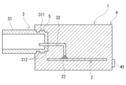
本開示の実施形態の詳細を、以下に図面を参照しつつ説明する。図3は、実施形態のコネクタ装置において、コネクタに備わる端子の長手方向に平行な平面で切断した切断面である。端子の長手方向は、主にハウジングの内側に位置する端子の長手方向のことであり、コネクタに備わる筒状のハウジングの軸方向と平行な方向のことを言う。各図において、溶着部はクロスハッチングで示す。図中の同一符号は同一名称物を示す。
[Details of the embodiment of the present disclosure]
Details of embodiments of the present disclosure are described below with reference to the drawings. FIG. 3 is a cross-sectional view taken along a plane parallel to the longitudinal direction of the terminals provided in the connector in the connector device of the embodiment. The longitudinal direction of the terminal is the longitudinal direction of the terminal mainly located inside the housing, and is parallel to the axial direction of the cylindrical housing provided in the connector. In each figure, welded portions are indicated by cross hatching. The same reference numerals in the drawings indicate the same names.
<コネクタ装置>
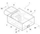
実施形態のコネクタ装置1は、図1から図3に示すように、回路基板2とコネクタ3とを備える。回路基板2は、導体路20を備える。コネクタ3は、ハウジング31と端子32とを備える。ハウジング31は、樹脂で構成される筒状である。端子32は、ハウジング31の軸方向外側に突出し、導体路20に接続される。実施形態のコネクタ装置1は、回路基板2と、ハウジング31の外側に位置する端子32と、ハウジング31の一部とをまとめて覆うモールド樹脂部4を備える点を特徴の一つとする。また、実施形態のコネクタ装置1は、ハウジング31におけるモールド樹脂部4と接触する全周にわたって設けられる突起部311を備え、この突起部311に溶着部5を備える点を特徴の一つとする。以下、各構成を詳細に説明する。
<Connector device>
A
〔回路基板〕
回路基板2は、半導体リレー等の電子部品(図示略)やコネクタ3等が実装される板状部材である。回路基板2は、プリント基板を用いることができる。回路基板2は、導体路20を備える。導体路20は、回路基板2の電気回路を構成する導電部材のうち、表面に露出している箇所をいう。導体路20は、例えば、回路基板2の導電パターン21、回路基板2に実装された電子部品の端子(図示略)、電子部品の端子やコネクタ3の端子32と導電パターン21とを接続する半田22等を含む。回路基板2は、後述するモールド樹脂部4に埋設される。
[Circuit board]
The
〔コネクタ〕
コネクタ3は、相手側コネクタ(図示略)が接続される接続部材である。相手側コネクタは、ワイヤーハーネスを介して車載電装品等と接続されている。コネクタ3は、回路基板2に実装される。コネクタ3は、ハウジング31と端子32とを備える。コネクタ3は、更に取付部33と固定部材34(図2)とを備える。コネクタ3は、回路基板2の延長面に対して間隔を有するように配置されている。図1から図3に示すコネクタ3は、回路基板2よりも上方に配置されている。
〔connector〕
The
〈ハウジング〉
ハウジング31は、相手側コネクタが嵌め込まれる筒状部材である。ハウジング31は、相手側コネクタが嵌め込まれる側が開口し、その開口側と反対側が閉塞した有底筒状である。この閉塞した面には、後述する端子32が貫通する。つまり、端子32は、この閉塞した面を通ってハウジング31の内側から外側に向かって引き出される。以下、この閉塞した面を閉塞端面と呼ぶことがある。ハウジング31の外側に位置する端子32は、この閉塞端面から突出する。ハウジング31における閉塞端面及び閉塞端面近傍は、全周にわたって後述するモールド樹脂部4に埋設される。ハウジング31は、図3に示すように、閉塞端面近傍の外周に突起部311を備える。突起部311も、モールド樹脂部4に埋設される。
<housing>
The
≪突起部≫
突起部311は、ハウジング31の全周にわたって設けられている。突起部311は、後述する溶着部5を備える。溶着部5は、代表的には、レーザー溶着により構成される。詳細は後述するが、溶着部5は、レーザーによる熱によって、ハウジング31とモールド樹脂部4の互いの構成材料が溶着されて構成される。突起部311は、溶着部5を構成する際に、レーザーの熱を集中的に吸収する機能を有する。突起部311の形状や寸法は、レーザー溶着の前後で実質的に変化しない。
≪Protrusion≫
The projecting
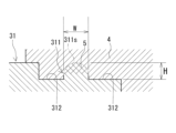
本例のハウジング31は、全周にわたって設けられると共に、ハウジング31の軸方向に並列される複数の凹部312を備える。突起部311は、隣り合う凹部312の側壁を構成するように設けられている。本例では、二つの凹部312が設けられている。
The
突起部311は、レーザーの熱を集中的に吸収できる形状を適宜選択できる。突起部311は、ハウジング31の軸方向に平行な先端面311s(図4)を備えることが好ましい。ハウジング31の軸方向は、ハウジング31の内側に位置する端子32(図3)の長手方向に等しい。突起部311に先端面311sを備えることで、突起部311におけるレーザーを受ける面を安定して確保し易い。また、突起部311が先端面311sを備えることで、レーザーの熱が発生する領域を突起部311の先端側に設け易く、熱が突起部311の基端側に伝わることを抑制し易い。
The
突起部311の横断面形状は、特に限定されない。この横断面形状は、図4に示すように、四角形であることが挙げられる。突起部311の横断面形状は、突起部311が延びる方向と直交する方向に切断した切断面における形状である。突起部311が突出する方向は、ハウジング31の径方向である。突起部311がハウジング31の周方向に延びる形態は、ハウジング31の周方向に沿って設けられる構成でもよいし、波形など、ハウジング31の周方向からずれる屈曲した構成であってもよい。突起部311の横断面形状が四角形であると、突起部311の形状が単純であり、突起部311とモールド樹脂部4との密着性を向上し易い。また、突起部311の横断面形状が四角形であると、突起部311を製造し易い。
The cross-sectional shape of the
突起部311の最大幅W(図4)は、1mm以上2mm未満であることが好ましい。突起部311の最大幅Wが1mm以上であることで、レーザーを受ける面を確保し易く、レーザーの熱が突起部311に集中し易い。一方、突起部311の最大幅Wが2mm未満であることで、レーザーの強度分布にもよるが、レーザーの熱が突起部311に集中し易い。突起部311の最大幅Wは、更に1mm以上1.7mm以下、特に1mm以上1.5mm以下であることが挙げられる。
A maximum width W (FIG. 4) of the
突起部311の最大高さH(図4)は、0.2mm以上0.5mm以下であることが好ましい。突起部311の最大高さHが0.2mm以上であることで、レーザーの熱が発生する領域を突起部311の先端側に設け易く、熱が突起部311の基端側に伝わることを抑制し易い。一方、突起部311の最大高さHが0.5mm以下であることで、レーザーによる熱の拡散が一定になり易く、突起部311における構成材料の溶融が一定になり易い。突起部311の最大高さHは、更に0.2mm以上0.4mm以下、特に0.2mm以上0.3mm以下であることが挙げられる。
The maximum height H (FIG. 4) of the
突起部311の横断面形状は、図5に示すように、三角形であってもよい。また、突起部311の横断面形状は、図6に示すように、先端面311sが円弧面で構成される半円形であってもよい。また、突起部311の横断面形状は、台形であってもよい(図示略)。また、突起部311の横断面形状は、先端側から基端側に向かって幅が狭くなるような逆台形であってもよい(図示略)。
The cross-sectional shape of the
突起部311は、図3に示すように、ハウジング31の内側に位置する端子32に対して交差するように設けられている。突起部311は、ハウジング31の全周にわたって設けられている。つまり、突起部311は、環状に設けられている。よって、ハウジング31の内側に位置する端子32は、環状の突起部311の内周側に挿通して配置されることになる。この場合、ハウジング31からの端子32の突出箇所である閉塞端面が突起部311と近い。この場合であっても、突起部311に熱が集中することで、レーザーの熱により端子32、及び端子32に接続される回路基板2に悪影響が及ぶことを抑制できる。
As shown in FIG. 3, the projecting
複数の凹部312のうち、ハウジング31の閉塞端面側に位置する凹部312は、上記閉塞端面につながる切欠きで構成されている。ハウジング31の閉塞端面側とは、図3の右側である。複数の凹部312のうち、ハウジング31の開口側に位置する凹部312は、両側に側壁を有する溝で構成されている。ハウジング31の開口側とは、図3の左側である。
Of the plurality of
本例の凹部312の深さは、突起部311の最大高さと同じである。このような凹部312によって突起部311を構成することで、凹部312がない場合に比較して、ハウジング31の外表面から突出する突起部311の突出量を小さくできる。ハウジング31の外表面からの突起部311の突出量が小さいと、ハウジング31の外表面からのモールド樹脂部4の厚さを小さくし易く、小型化し易い。
The depth of the
凹部312には、モールド樹脂部4が充填される。そのため、凹部312に充填されるモールド樹脂部4がアンカーとなることに加え、突起部311が一様な高さで凹部312を備えない場合に比較して、ハウジング31とモールド樹脂部4との接触面積を大きくできる。よって、凹部312を備えることで、ハウジング31とモールド樹脂部4との密着性が向上され易い。
The
凹部312は、三つ以上であってもよい。この場合、二つの突起部311が、ハウジング31の軸方向に並列して設けられる。凹部312は、一つであってもよい。この場合、突起部311の側壁は、一方が凹部312の側壁で構成され、他方がハウジング31の閉塞端面で構成される。凹部312はなくてもよい。この場合、突起部311は、ハウジング31の外表面から突出することになる。
The number of
≪透過率≫
ハウジング31の透過率は、低いことが好ましい。ハウジング31の透過率は、波長が940nmのレーザーの光量a2と、ハウジング31の構成材料からなる厚さ2mmの試験片を上記レーザーが透過した光量b2との比率(b2/a2)×100である。透過率の低いハウジング31は、上記レーザーを吸収し易い。即ち、透過率の低いハウジング31は、上記レーザーによって溶け易い。そのため、後述する溶着部5が形成され易い。ハウジング31の透過率は、例えば、10%以下が好ましい。透過率が10%以下のハウジング31は、上記レーザーを吸収し易く溶け易いため、溶着部5を形成し易い。ハウジング31の透過率は、更に7%以下が好ましく、特に5%以下が好ましい。ハウジング31の色は、不透明な黒色や灰色等であることが好ましい。これらの色は、上記レーザーを吸収し易い。
≪Transmittance≫
It is preferable that the transmittance of the
≪材質≫
ハウジング31は、例えば、ポリエステルを含むことが好ましい。ポリエステルは、電気絶縁性、耐水性等に優れる。そのため、ポリエステルを含むハウジング31は、ハウジング31の内側にある端子32等を機械的、電気的、化学的に保護し易い。ポリエステルとしては、代表的には、ポリブチレンテレフタレート(PBT)が挙げられる。ハウジング31は、更に、着色剤を含んでいることが好ましい。着色剤は、ハウジング31の透過率が低くなるものが挙げられる。着色剤としては、例えば、カーボンブラックが挙げられる。カーボンブラックを含むことで、ハウジング31の色が黒色となり易い。
≪Material≫
〈端子〉
端子32は、相手側コネクタと回路基板2とを電気的に接続する。端子32は、ハウジング31の閉塞端面を貫通し、ハウジング31の内側から外側に向かって引き出される。端子32のうち、ハウジング31の内側に位置する部分は、ハウジング31の軸方向に沿って設けられている。ハウジング31の内側に位置する端子32の一端は、相手側コネクタに電気的に接続される。端子32のうち、ハウジング31の外側に位置する部分は、回路基板2側に延びるように屈曲されている。本例の端子32は、実質的に直角に屈曲された金属線で構成されている。ハウジング31の外側に位置する端子32の他端は、回路基板2の導電パターン21に電気的に接続される。端子32の他端と導電パターン21との電気的な接続には、半田22が利用できる。端子32はプレスフィット端子でもよい。この場合、端子32は圧入によって導電パターン21と電気的に接続される。よって、端子32がプレスフィット端子の場合、半田22を省略できる。端子32の他端は、回路基板2を貫通する。ハウジング31の外側に位置する端子32は、モールド樹脂部4に埋設される。
<Terminal>
The
〈取付部〉
取付部33は、ハウジング31に一体に設けられている。本例では、取付部33は、ハウジング31の一部として一体成形されている。取付部33は、ハウジング31の閉塞端面から回路基板2側に延びるようにL字状に屈曲されている。本例の取付部33は、実質的に直角に屈曲された丸棒部材で構成されている。本例では、二つの取付部33が、端子32を挟むように設けられている。取付部33の端面には、ネジ穴が設けられている。このネジ穴には、後述する固定部材34が取り付けられる。取付部33の端面と固定部材34とで回路基板2を挟むことで、回路基板2とハウジング31とが固定される。取付部33は、モールド樹脂部4に埋設される。
<Mounting part>
The mounting
〈固定部材〉
固定部材34は、ハウジング31を回路基板2に固定する。固定部材34には、例えばネジを用いることができる。本例の固定部材34は、樹脂製のネジで構成されている。本例では、二つの固定部材34がそれぞれ、回路基板2に設けられた挿通孔(図示略)に貫通され、各取付部33に取り付けられる。固定部材34の取付部33に対する取り付けによって、ハウジング31が回路基板2に固定される。固定部材34の一部は、回路基板2の表面から突出している。固定部材34は、モールド樹脂部4に埋設される。
<Fixing member>
The fixing
〔モールド樹脂部〕
モールド樹脂部4は、回路基板2や端子32等の導電部材を外部環境から機械的、電気的、化学的に保護する。モールド樹脂部4は、回路基板2と、ハウジング31の外側に位置する端子32と、ハウジング31の一部とをまとめて覆う。本例では、モールド樹脂部4は、回路基板2と、コネクタ3の大部分とをまとめて覆う。コネクタ3の大部分とは、ハウジング31における相手側コネクタが嵌め込まれる開口側の端部を除く領域である。
[Mold resin part]
The molded
モールド樹脂部4は、大気に接する表面を有する。大気に接するとは、コネクタ装置1がケース等で覆われておらず露出されており、コネクタ装置1における最外面を構成することをいう。本例では、モールド樹脂部4の表面は、全域にわたって大気に接する。即ち、コネクタ装置1は、ケースレスである。そのため、コネクタ装置1は小型である。
The
≪透過率≫
モールド樹脂部4の透過率は、高いことが好ましい。モールド樹脂部4の透過率は、波長が940nmのレーザーの光量a1と、モールド樹脂部4の構成材料からなる厚さ2mmの試験片を上記レーザーが透過した光量b1との比率(b1/a1)×100である。透過率の高いモールド樹脂部4は、上記レーザーを吸収し難くハウジング31に到達させ易い。そのため、後述する溶着部5が形成され易い。モールド樹脂部4の透過率は、例えば、40%以上が好ましい。透過率が40%以上のモールド樹脂部4は、上記レーザーを透過させ易いため、溶着部5を形成し易い。モールド樹脂部4の透過率は、更に45%以上が好ましく、特に50%以上が好ましい。モールド樹脂部4の色は、無色透明や白色透明、不透明な白色などであることが好ましい。これらの色は、上記レーザーを透過させ易い。
≪Transmittance≫
It is preferable that the transmittance of the
≪材質≫
モールド樹脂部4は、例えば、ポリアミド樹脂、又はポリエステルを含むことが好ましい。ポリアミド樹脂は、機械的強度等に優れる。そのため、ポリアミド樹脂を含むモールド樹脂部4は、モールド樹脂部4で覆われる部材を機械的に保護し易い。ポリエステルは、電気絶縁性、耐水性等に優れる。そのため、ポリエステルを含むモールド樹脂部4は、モールド樹脂部4で覆われる部材を電気的かつ化学的に保護し易い。
≪Material≫
The
ハウジング31とモールド樹脂部4とは同種の樹脂を含むことが好ましい。特に、ハウジング31とモールド樹脂部4とは、全く同じ樹脂で構成されることが好ましい。ハウジング31とモールド樹脂部4とが同種の樹脂を含むことで、ハウジング31とモールド樹脂部4との溶解度パラメータを近くし易い。そのため、ハウジング31とモールド樹脂部4とは互いになじみ性が良い。その上、後述する溶着部5が同種の樹脂を含むことで、溶着部5自体の強度が高くなり易い。よって、ハウジング31とモールド樹脂部4との密着性がより高い。例えば、ハウジング31がポリエステルを含む場合、モールド樹脂部4はポリエステルを含むことが好ましい。
It is preferable that the
モールド樹脂部4は、射出成形体であることが好ましい。射出成形体は、射出成形により作製できる。射出成形は、圧力をかけながらモールド樹脂部4の構成材料を成形金型内に充填して回路基板2やハウジング31等を覆う。そのため、射出成形は、注型成形に比べて、モールド樹脂部4の構成材料を成形金型の隅々まで充填し易い。よって、射出成形体は、注型成形体に比べて、回路基板2やハウジング31等とモールド樹脂部4との間に隙間が形成され難い。隙間が形成され難いことで、隙間内の水蒸気が結露して水滴が生成され難い。また、射出成形体は、モールド樹脂部4の形状の自由度が高い。
The molded
モールド樹脂部4の構成材料は、融点が180℃以上200℃以下であることが好ましい。上記構成材料の融点が180℃以上であることで、コネクタ装置1の使用時にモールド樹脂部4が溶けて変形することを防止できる。一方、上記構成材料の融点が200℃以下であることで、射出成形時の成形温度を200℃以下に設定することができ、その成形温度で半田22等が溶けることを防止できる。
The constituent material of the
モールド樹脂部4は、射出成形体であるため、ゲートの痕跡部40を備える。痕跡部40は、モールド樹脂部4の成形時に金型のキャビティにモールド樹脂部4の構成材料を充填するためのゲートに対応する箇所である。射出成形により作製されたモールド樹脂部4には、ゲートに対応する部分を有する付属部が形成される。この付属部を除去することで、モールド樹脂部4にはゲートの痕跡部40が形成される。この付属部は、ゲートに対応する部分の他、スプルーに対応する部分を有することがあり、更にはランナーに対応する部分を有することもある。付属部の除去は、例えば、付属部を折り取ることで行える。ハウジング31の周辺には端子32等が配置されるため、射出成形時のゲートは、ハウジング31から離れた位置に設定されることが好ましい。よって、痕跡部40は、モールド樹脂部4におけるハウジング31とは反対側に設けられることが好ましい。
Since the molded
〔溶着部〕
溶着部5は、図4に示すように、ハウジング31とモールド樹脂部4の互いの構成材料が溶着されてなる。溶着とは、互いの構成材料が混ざり合っていること、互いの構成材料が相溶していること、せん断力によって界面破壊ではなく材料破壊が生じること、コネクタ3の表面が粗面になっていること、の少なくとも一つを満たすことをいう。界面破壊とは、ハウジング31とモールド樹脂部4との界面で破壊が生じることをいう。そのため、ハウジング31とモールド樹脂部4とが互いの界面に沿って剥離する。よって、ハウジング31及びモールド樹脂部4の一方の部材に他方の部材の構成材料が付着しない。材料破壊とは、ハウジング31とモールド樹脂部4の一方の部材の内部で破壊が生じることをいう。そのため、他方の部材における一方の部材との対向面に一方の部材の構成材料が付着した状態で両部材が分離する。溶着部5は、ハウジング31とモールド樹脂部4との密着性を高められる。
[Welding part]
As shown in FIG. 4, the
溶着部5は、ハウジング31に設けられる突起部311に構成される。突起部311は、上述したように、ハウジング31の全周にわたって設けられている。よって、溶着部5も、ハウジング31の全周にわたって設けられている。そのため、ハウジング31とモールド樹脂部4との間から水等の液体が浸入することを抑制できる。よって、回路基板2や端子32等の導電部材に液体が付着することを抑制できる。
The welded
〔用途〕
実施形態のコネクタ装置1は、自動車のエンジンコントロールユニットや自動車の電動ブレーキシステムのモジュール等に好適に利用できる。エンジンコントロールユニットとしては、例えば、燃料噴射制御のエンジンコントロールユニット(Fuel Injection Engine Control Unit:FI-ECU)が挙げられる。電動ブレーキシステムのモジュールとしては、電動機械ブレーキ(Electro Mechanical Brake:EMB)や電動パーキングブレーキ(Electronic Parking Brake:EPB)のモジュールが挙げられる。
[Use]
The
<コネクタ装置の製造方法>
上述したコネクタ装置1は、回路基板2及びコネクタ3を含む組物を準備する工程と、準備した組物の一部をモールド樹脂部4で覆った一体物を構成する工程と、一体物にレーザーを照射する工程とによって製造できる。
<Manufacturing Method of Connector Device>
The above-described
〔組物を準備する工程〕
組物を準備する工程では、上述した回路基板2とコネクタ3とが接続された組物を準備する。組物は、回路基板2の導電パターン21とコネクタ3の端子32とが半田22で電気的に接続されている。また、組物は、コネクタ3の取付部33が固定部材34によって回路基板2に固定されて構成されている。
[Step of preparing braid]
In the step of preparing a braid, a braid in which the
〔一体物を構成する工程〕
一体物を構成する工程では、回路基板2と、コネクタ3におけるハウジング31の外側に位置する端子32と、ハウジング31の一部とをまとめてモールド樹脂部4で覆う。つまり、一体物を構成する工程では、組物のうち、コネクタ3におけるハウジング31の相手側コネクタが嵌め込まれる開口を除く大部分をモールド樹脂部4で覆う。モールド樹脂部4は、ハウジング31に設けられた突起部311を覆うと共に、凹部312に充填される。
[Step of forming an integral object]
In the step of constructing the integrated body, the
〔レーザーを照射する工程〕
レーザーを照射する工程では、モールド樹脂部4を通してハウジング31に設けられた突起部311にレーザーを照射し、ハウジング31とモールド樹脂部4の互いの構成材料を溶着する。レーザーの照射は、ハウジング31の外周面の法線方向におけるモールド樹脂部4の外側から行うことが挙げられる。モールド樹脂部4はレーザーを透過し、ハウジング31はレーザーを吸収する。レーザーを吸収したハウジング31は発熱し、その発熱によってハウジング31の構成材料が溶融する。ハウジング31における溶融熱がモールド樹脂部4に伝わることでモールド樹脂部4が発熱し、その発熱によってモールド樹脂部4が溶融する。溶融したハウジング31の構成材料とモールド樹脂部4の構成材料とが接着した状態で固化することで、溶着部5が構成される。
[Step of irradiating laser]
In the step of irradiating the laser, the projecting
レーザーの照射条件は、適宜選択できる。レーザー源の種類は、固体レーザー、半導体レーザー、ファイバーレーザー等が挙げられる。レーザーの波長は、例えば、800nm以上990nm以下、更に850nm以上990nm以下、特に930nm以上950nm以下が挙げられる。レーザーの波長は、940nmが好適である。レーザーの出力は、ハウジング31及びモールド樹脂部4の材質によるが、例えば、10W以上100W以下、更に20W以上90W以下、特に30W以上60W以下が挙げられる。
The laser irradiation conditions can be appropriately selected. Types of laser sources include solid-state lasers, semiconductor lasers, fiber lasers, and the like. The wavelength of the laser is, for example, 800 nm or more and 990 nm or less, further 850 nm or more and 990 nm or less, and particularly 930 nm or more and 950 nm or less. A suitable laser wavelength is 940 nm. The output of the laser depends on the materials of the
レーザーの照射は、例えば、ハウジング31の周方向に走査させながら行うことが挙げられる。レーザーの走査速度は、ハウジング31及びモールド樹脂部4の材質、厚み、形状にもよるが、例えば、5mm/min以上50mm/min以下、更に10mm/min以上40mm/min以下、特に20mm/min以上30mm/min以下が挙げられる。他に、レーザーの照射は、ハウジング31の全周に対して一括して行うことが挙げられる。この場合、レーザーの照射光源をハウジング31の周方向に複数並べて配置し、同時にレーザーの照射を行う。レーザーの照射は、モールド樹脂部4をハウジング31側に押し付けた状態で行うことが好ましい。そうすることで、モールド樹脂部4とハウジング31との密着性が向上され易い。
Laser irradiation may be performed while scanning the
<効果>
実施形態のコネクタ装置1は、以下の効果を奏することができる。
<effect>
The
(1)防水性能に優れる。溶着部5によりハウジング31とモールド樹脂部4との密着性を高められるため、ハウジング31とモールド樹脂部4との隙間から液体の浸入を抑制し易いからである。特に、突起部311でレーザーによる熱を発生させて溶着部5が構成されるため、レーザーによる熱を突起部に集中し易く、強固な溶着部5が構成され易い。よって、モールド樹脂部4で覆われる回路基板2や端子32等の導電部材に液体が付着することを抑制できる。
(1) Excellent waterproof performance. This is because the adhesion between the
(2)小型化し易い。モールド樹脂部4で回路基板2や端子32等の導電部材をまとめて覆っていることで、回路基板2等を収納する筐体を別途備える必要がない。筐体を備えないことで、筐体間を防水するシール材も備える必要がない。
(2) It is easy to miniaturize. Since the conductive members such as the
(3)製造し易い。実施形態のコネクタ装置1は、上述したように溶着部5により防水性能に優れるため、筐体及びシール材が不要なため、部品点数が少なく、筐体を組み立てる作業やシール材を配置する作業を省略できるからである。
(3) Easy to manufacture. Since the
[試験例]
ハウジングに設けた突起部に溶着部を備えるコネクタ装置を作製し、突起部の形状や大きさの違いによる接着性能の違いを調べた。接着性能の評価は、図7に示す試験片100を用いて行った。試験片100は、コネクタのハウジングとモールド樹脂部との接合箇所を模擬した部材である。
[Test example]
A connector device having a welded portion on a projection provided on a housing was manufactured, and the difference in adhesion performance due to the difference in the shape and size of the projection was investigated. Evaluation of adhesion performance was performed using a
<試験片>
〔試料No.1-1~1-5〕
ハウジングにおけるモールド樹脂部との接合箇所を模擬した吸収材110を準備した。吸収材110は、透過率が1%のPBT樹脂で構成される。吸収材110は、長さが80mm、幅が25mm、厚さが1mmの板材である。吸収材110における端部近傍の表面には、突起部111と凹部112とを設けた。具体的には、凹部112として、吸収材110における端面につながる切欠きと、この切欠きに並列した溝部とを、吸収材110の幅方向に沿って設けた。突起部111は、この切欠きと溝部との各側壁を構成するように、吸収材110の幅方向に沿って設けた。突起部111の横断面形状は、図4に示すような四角形とした。突起部111の幅Wと高さH(図4)は、表1に示す。突起部111の高さHの調整は、突起部111の先端が吸収材110の表面から突出しないように、凹部112の深さを調整することで行った。
<Test piece>
[Sample No. 1-1 to 1-5]
An absorbing
準備した吸収材110の突起部111及び凹部112を覆うように透過材120を射出成形した。透過材120は、透過率が40%の熱可塑性ポリエステル樹脂で構成される。熱可塑性ポリエステル樹脂は、東洋紡株式会社製バイロショット(登録商標)を用いた。透過材120は、吸収材110における突起部111及び凹部112が設けられた表面側に接触すると共に、吸収材110の長手方向に沿って延びるように形成した。透過材120は、長さが80mm、幅が25mm、吸収材110の表面からの厚さが1mmとした。吸収材110と透過材120とが重複する領域の長さは、10mmとした。
A
透過材120を通して吸収材110に設けられた突起部111にレーザーを照射した。レーザーの照射は、吸収材110の表面の法線方向における透過材120の上方から行った。また、レーザーの照射は、透過材120を吸収材110側に押し付けながら、突起部111の幅方向全域にわたって一括して行った。押し付け圧力は、0.1MPaとした。レーザーのスポット径は1.5mmとした。レーザーの波長は、940nmとした。その結果、突起部111の先端部に溶着部150が形成された。
A
〔試料No.2-1~2-3〕
試料No.2-1~2-3では、試料No.1-1~1-5に対して、突起部111の形状及び大きさを変更した。突起部111の横断面形状は、図5に示すような三角形とした。突起部111の幅Wと高さH(図5)は、表1に示す。突起部111の形状及び大きさ以外の条件は、試料No.1-1~1-5と同様とした。
[Sample No. 2-1 to 2-3]
Sample no. In 2-1 to 2-3, sample No. The shape and size of the
〔試料No.3-1~3-2〕
試料No.3-1~3-2では、試料No.1-1~1-5に対して、突起部111の形状及び大きさを変更した。突起部111の横断面形状は、図6に示すような半円形とした。突起部111の幅Wと高さH(図6)は、表1に示す。突起部111の形状及び大きさ以外の条件は、試料No.1-1~1-5と同様とした。
[Sample No. 3-1 to 3-2]
Sample no. In 3-1 and 3-2, sample No. The shape and size of the
〔試料No.100〕
試料No.100では、吸収材110に突起部111を設けなかった。試料No.100では、吸収材110と透過材120とが重複する任意の領域において、吸収材110と透過材120との幅方向全域にわたって一括してレーザーを照射した。突起部111以外の条件は、試料No.1-1~1-5と同様とした。
[Sample No. 100]
Sample no. In 100, the
<接着性能の評価>
得られた各試料の試験片100について、せん断引張試験を行って、接着性能の評価を行った。せん断引張試験の装置には、株式会社島津製作所製のオートグラフAGS-Xシリーズを用いた。せん断引張試験は、図7の白抜き矢印に示すように、吸収材110と透過材120とを長さ方向に沿って互いが離れる方向へ引っ張り、吸収材110と透過材120とが分離したときの最大引張応力を求めた。各試料の測定数は5とした。最大引張応力の平均値を表1に示す。
<Evaluation of adhesion performance>
A
また、吸収材110と透過材120における接着面を目視にて観察した。その結果、いずれの試料も溶着部150において、材料破壊が生じていた。材料破壊では、吸収材110及び透過材120の一方の内部で破壊が生じており、分離した他方の表面に一方の構成材料が付着していた。
In addition, the bonding surface between the absorbing

表1に示すように、突起部を備える試料No.1-1~1-5、No.2-1~2-3、3-1~3-2は、最大引張応力が2.00MPa以上であり、突起部を備えない試料No.100よりも接着性能に優れる。突起部を備える場合、レーザーによる熱を突起部に集中することができ、突起部に強固な溶着部が構成されたと考えられる。 As shown in Table 1, sample no. 1-1 to 1-5, No. Sample Nos. 2-1 to 2-3 and 3-1 to 3-2 have a maximum tensile stress of 2.00 MPa or more and do not have protrusions. Adhesion performance is superior to that of 100. It is considered that when the protrusion is provided, the heat generated by the laser can be concentrated on the protrusion, and a strong welded portion is formed on the protrusion.
突起部の形状に関して、試料No.1-1とNo.2-1とNo.3-1とを比較すると、突起部の形状が四角形である試料No.1-1は、突起部の形状が三角形や半円形である試料No.2-1、No.3-1よりも接着性能に優れる。また、試料No.1-3とNo.2-2とNo.3-2とを比較すると、突起部の形状が四角形である試料No.1-3は、突起部の形状が三角形や半円形である試料No.2-2、No.3-2よりも接着性能に優れる。突起部が四角形である場合、吸収材と透過材とを密着させ易く、かつレーザーを受ける面を安定して確保でき、突起部により強固な溶着部が構成されたからと考えられる。 With respect to the shape of the protrusion, sample No. 1-1 and No. 2-1 and No. 3-1, Sample No. 3-1 has a rectangular protrusion. Sample No. 1-1 has a triangular or semicircular protrusion. 2-1, No. Adhesion performance is superior to that of 3-1. Moreover, sample no. 1-3 and No. 2-2 and No. 3-2, Sample No. 3-2 has a rectangular protrusion. Sample No. 1-3 has a triangular or semicircular protrusion. 2-2, No. Adhesion performance is superior to that of 3-2. This is probably because, when the protrusions are square, the absorber and the transmission material can be easily brought into close contact with each other, and the laser-receiving surface can be stably secured, and the protrusions form a strong welded portion.
突起部の幅に関して、試料No.1-1とNo.1-3とを比較すると、突起部の幅が小さい試料No.1-1は、突起部の幅が大きい試料No.1-3よりも接着性能に優れる。また、試料No.2-1とNo.2-2とを比較すると、突起部の幅が小さい試料No.2-1は、突起部の幅が大きい試料No.2-2よりも接着性能に優れる。また、試料No.3-1とNo.3-2とを比較すると、突起部の幅が小さい試料No.3-1は、突起部の幅が大きい試料No.3-2よりも接着性能に優れる。突起部の幅が小さい場合、レーザーのスポット径によらずレーザーを受ける面を安定して確保でき、突起部により強固な溶着部が構成されたからと考えられる。 With respect to the width of the protrusion, sample No. 1-1 and No. A comparison with Sample No. 1-3 shows that sample No. 1, which has a small protrusion width. 1-1 is sample No. 1, which has a large protrusion width. Adhesion performance is superior to that of 1-3. Moreover, sample no. 2-1 and No. 2-2, Sample No. 2, which has a small protrusion width. 2-1 is sample No. 2, which has a large protrusion width. Adhesion performance is superior to that of 2-2. Moreover, sample no. 3-1 and No. 3-2, Sample No. 3-2 has a small protrusion width. 3-1 is sample No. 3, which has a large protrusion width. Adhesion performance is superior to that of 3-2. This is probably because when the width of the protrusion is small, the surface that receives the laser can be stably secured regardless of the laser spot diameter, and the protrusion forms a strong welded portion.
突起部の高さに関して、試料No.1-1とNo.1-2とを比較すると、接着性能に大きな優劣は見受けられない。また、試料No.1-3とNo.1-4とNo.1-5とを比較しても、接着性能に大きな優劣は見受けられない。ここで、試料No.1-3とNo.1-4とNo.1-5において、最大引張応力のばらつきに関して検討した。各試料の測定数は5であり、この測定数における最大引張応力のばらつきを求めた。その結果、突起部の高さが小さいほど、ばらつきが小さくなることがわかった。突起部の高さが小さい場合、レーザーによる熱の拡散が一定になり易く、突起部における構成材料の溶融が一定になったからと考えられる。なお、突起部の高さが0.2mm以上であることで、レーザーの熱が突起部に集中し易いと考えられる。 With respect to the height of the protrusion, sample No. 1-1 and No. A comparison with 1-2 shows no significant superiority or inferiority in adhesion performance. Moreover, sample no. 1-3 and No. 1-4 and No. A comparison with 1-5 does not reveal any significant superiority or inferiority in adhesion performance. Here, sample no. 1-3 and No. 1-4 and No. In 1-5, the variation of the maximum tensile stress was examined. The number of measurements for each sample was 5, and the variation in the maximum tensile stress was determined for this number of measurements. As a result, it was found that the smaller the height of the protrusion, the smaller the variation. This is probably because when the height of the projection is small, the diffusion of heat by the laser tends to be constant, and the melting of the constituent material at the projection is constant. In addition, it is considered that the heat of the laser tends to be concentrated on the protrusion when the height of the protrusion is 0.2 mm or more.
本発明は、これらの例示に限定されるものではなく、特許請求の範囲によって示され、特許請求の範囲と均等の意味および範囲内でのすべての変更が含まれることが意図される。 The present invention is not limited to these exemplifications, but is indicated by the scope of the claims, and is intended to include all modifications within the meaning and scope of equivalents of the scope of the claims.
1 コネクタ装置
2 回路基板
20 導体路、21 導電パターン、22 半田
3 コネクタ
31 ハウジング、311 突起部、311s 先端面、312 凹部
32 端子、33 取付部、34 固定部材
4 モールド樹脂部
40 痕跡部
5 溶着部
100 試験片
110 吸収材、111 突起部、112 凹部
120 透過材
150 溶着部
W 幅、H 高さ
REFERENCE SIGNS
Claims (15)
コネクタと、
モールド樹脂部とを備え、
前記回路基板は、導体路を備え、
前記コネクタは、
樹脂で構成される筒状のハウジングと、
前記ハウジングの内側から前記ハウジングの軸方向外側に突出し、前記導体路に接続される端子とを備え、
前記モールド樹脂部は、前記回路基板と、前記ハウジングの外側に位置する前記端子と、前記ハウジングの一部とをまとめて覆い、
前記ハウジングは、前記モールド樹脂部に接触するように全周にわたって設けられる突起部を備え、
前記突起部は、前記ハウジングと前記モールド樹脂部の互いの構成材料が溶着されてなる溶着部を備える、
コネクタ装置。 a circuit board;
a connector;
and a mold resin part,
The circuit board comprises a conductor track,
The connector is
a cylindrical housing made of resin;
a terminal projecting from the inside of the housing to the axial outside of the housing and connected to the conductor path,
The molded resin portion collectively covers the circuit board, the terminals positioned outside the housing, and a portion of the housing,
The housing has a protrusion provided over the entire circumference so as to contact the mold resin portion,
The projecting portion includes a welded portion formed by welding together constituent materials of the housing and the mold resin portion,
connector device.
前記突起部は、隣り合う前記凹部の側壁を構成する請求項1に記載のコネクタ装置。 The housing is provided along the entire circumference so as to be in contact with the mold resin portion, and has a plurality of concave portions arranged in parallel in the axial direction thereof,
2. The connector device according to claim 1, wherein the projections form side walls of the adjacent recesses.
前記モールド樹脂部の透過率は、波長が940nmのレーザーの光量a1と、前記モールド樹脂部の構成材料からなる厚さ2mmの試験片を前記レーザーが透過した光量b1との比率(b1/a1)×100である。 The connector device according to any one of claims 1 to 7, wherein the transmittance of the mold resin portion is 40% or more.
The transmittance of the mold resin portion is the ratio (b1/a1) of the light amount a1 of the laser having a wavelength of 940 nm and the light amount b1 of the laser transmitted through a test piece having a thickness of 2 mm made of the constituent material of the mold resin portion. x100.
前記ハウジングの透過率は、波長が940nmのレーザーの光量a2と、前記ハウジングの構成材料からなる厚さ2mmの試験片を前記レーザーが透過した光量b2との比率(b2/a2)×100である。 9. The connector device according to any one of claims 1 to 8, wherein the housing has a transmittance of 10% or less.
The transmittance of the housing is the ratio (b2/a2)×100 of the light amount a2 of the laser having a wavelength of 940 nm and the light amount b2 of the laser transmitted through a test piece having a thickness of 2 mm made of the constituent material of the housing. .
Priority Applications (4)
| Application Number | Priority Date | Filing Date | Title |
|---|---|---|---|
| JP2020039412A JP7319594B2 (en) | 2020-03-06 | 2020-03-06 | connector device |
| PCT/JP2021/008562 WO2021177426A1 (en) | 2020-03-06 | 2021-03-04 | Connector device |
| US17/802,706 US20230092720A1 (en) | 2020-03-06 | 2021-03-04 | Connector device |
| CN202180016995.9A CN115152098A (en) | 2020-03-06 | 2021-03-04 | Connector device |
Applications Claiming Priority (1)
| Application Number | Priority Date | Filing Date | Title |
|---|---|---|---|
| JP2020039412A JP7319594B2 (en) | 2020-03-06 | 2020-03-06 | connector device |
Publications (3)
| Publication Number | Publication Date |
|---|---|
| JP2021141001A JP2021141001A (en) | 2021-09-16 |
| JP2021141001A5 JP2021141001A5 (en) | 2022-08-24 |
| JP7319594B2 true JP7319594B2 (en) | 2023-08-02 |
Family
ID=77614064
Family Applications (1)
| Application Number | Title | Priority Date | Filing Date |
|---|---|---|---|
| JP2020039412A Active JP7319594B2 (en) | 2020-03-06 | 2020-03-06 | connector device |
Country Status (4)
| Country | Link |
|---|---|
| US (1) | US20230092720A1 (en) |
| JP (1) | JP7319594B2 (en) |
| CN (1) | CN115152098A (en) |
| WO (1) | WO2021177426A1 (en) |
Citations (5)
| Publication number | Priority date | Publication date | Assignee | Title |
|---|---|---|---|---|
| JP2014103091A (en) | 2012-10-24 | 2014-06-05 | Auto Network Gijutsu Kenkyusho:Kk | Method of manufacturing waterproof electronic circuit unit, and electronic circuit unit |
| JP2014177051A (en) | 2013-03-15 | 2014-09-25 | Denso Corp | Method for laser welding weld material |
| JP2014194899A (en) | 2013-03-29 | 2014-10-09 | Yazaki Corp | Waterproof connector |
| WO2016084537A1 (en) | 2014-11-25 | 2016-06-02 | 日立オートモティブシステムズ株式会社 | Electronic control device |
| WO2019039244A1 (en) | 2017-08-25 | 2019-02-28 | 日立オートモティブシステムズ株式会社 | Resin-sealed on-board electronic control device |
Family Cites Families (4)
| Publication number | Priority date | Publication date | Assignee | Title |
|---|---|---|---|---|
| JPH0359673U (en) * | 1989-10-17 | 1991-06-12 | ||
| JPH1076528A (en) * | 1996-09-03 | 1998-03-24 | Fujitsu Ten Ltd | Mold structure and connector structure |
| JP2010040992A (en) * | 2008-08-08 | 2010-02-18 | Hitachi Ltd | Method of manufacturing electronic control device, its transfer molding equipment and electronic control device |
| JP5056717B2 (en) * | 2008-10-16 | 2012-10-24 | 株式会社デンソー | Mold package manufacturing method |
-
2020
- 2020-03-06 JP JP2020039412A patent/JP7319594B2/en active Active
-
2021
- 2021-03-04 US US17/802,706 patent/US20230092720A1/en active Pending
- 2021-03-04 WO PCT/JP2021/008562 patent/WO2021177426A1/en active Application Filing
- 2021-03-04 CN CN202180016995.9A patent/CN115152098A/en active Pending
Patent Citations (5)
| Publication number | Priority date | Publication date | Assignee | Title |
|---|---|---|---|---|
| JP2014103091A (en) | 2012-10-24 | 2014-06-05 | Auto Network Gijutsu Kenkyusho:Kk | Method of manufacturing waterproof electronic circuit unit, and electronic circuit unit |
| JP2014177051A (en) | 2013-03-15 | 2014-09-25 | Denso Corp | Method for laser welding weld material |
| JP2014194899A (en) | 2013-03-29 | 2014-10-09 | Yazaki Corp | Waterproof connector |
| WO2016084537A1 (en) | 2014-11-25 | 2016-06-02 | 日立オートモティブシステムズ株式会社 | Electronic control device |
| WO2019039244A1 (en) | 2017-08-25 | 2019-02-28 | 日立オートモティブシステムズ株式会社 | Resin-sealed on-board electronic control device |
Also Published As
| Publication number | Publication date |
|---|---|
| US20230092720A1 (en) | 2023-03-23 |
| WO2021177426A1 (en) | 2021-09-10 |
| JP2021141001A (en) | 2021-09-16 |
| CN115152098A (en) | 2022-10-04 |
Similar Documents
| Publication | Publication Date | Title |
|---|---|---|
| EP2953210B1 (en) | Vehicle-mounted electronic module | |
| JP5380749B2 (en) | Wire harness and manufacturing method thereof | |
| JP5454636B2 (en) | Electrical junction box | |
| JP6034029B2 (en) | Connection structure | |
| JP7078003B2 (en) | Connector device | |
| WO2019039244A1 (en) | Resin-sealed on-board electronic control device | |
| CN111755890B (en) | Connector device | |
| JP7319594B2 (en) | connector device | |
| JP2007165418A (en) | Thermistor device, and its manufacturing method | |
| US11251553B2 (en) | Connector device that includes welded portion | |
| CN110214397B (en) | Module connector | |
| JP2018181522A (en) | Electric connector | |
| JP7319595B2 (en) | CONNECTOR DEVICE AND METHOD FOR MANUFACTURING CONNECTOR DEVICE | |
| JP2007335254A (en) | Electronic control device | |
| CN109476091B (en) | Method for producing a laser-welded connection and composite component | |
| JPH0139181B2 (en) | ||
| JP5532825B2 (en) | Electrical junction box | |
| US20200313345A1 (en) | Connector device | |
| JP5370733B2 (en) | Electrical junction box | |
| KR102285351B1 (en) | Fixing device for printed circuit board | |
| JP2008192359A (en) | Flat cable | |
| US20240145124A1 (en) | Water-proof structure for electric wire and water-proof method for electric wire | |
| JP2004103306A (en) | Socket for discharge lamp for vehicle and the discharge lamp for the vehicle | |
| JP4740747B2 (en) | Electrical junction box | |
| JP2013008447A (en) | Manufacturing method of wire harness |
Legal Events
| Date | Code | Title | Description |
|---|---|---|---|
| A521 | Request for written amendment filed |
Free format text: JAPANESE INTERMEDIATE CODE: A523 Effective date: 20220816 |
|
| A621 | Written request for application examination |
Free format text: JAPANESE INTERMEDIATE CODE: A621 Effective date: 20220930 |
|
| TRDD | Decision of grant or rejection written | ||
| A01 | Written decision to grant a patent or to grant a registration (utility model) |
Free format text: JAPANESE INTERMEDIATE CODE: A01 Effective date: 20230621 |
|
| A61 | First payment of annual fees (during grant procedure) |
Free format text: JAPANESE INTERMEDIATE CODE: A61 Effective date: 20230704 |
|
| R150 | Certificate of patent or registration of utility model |
Ref document number: 7319594 Country of ref document: JP Free format text: JAPANESE INTERMEDIATE CODE: R150 |