JP7307738B2 - Monolithic neural interface system - Google Patents
Monolithic neural interface system Download PDFInfo
- Publication number
- JP7307738B2 JP7307738B2 JP2020545070A JP2020545070A JP7307738B2 JP 7307738 B2 JP7307738 B2 JP 7307738B2 JP 2020545070 A JP2020545070 A JP 2020545070A JP 2020545070 A JP2020545070 A JP 2020545070A JP 7307738 B2 JP7307738 B2 JP 7307738B2
- Authority
- JP
- Japan
- Prior art keywords
- chip
- electrodes
- layer
- neural
- signals
- Prior art date
- Legal status (The legal status is an assumption and is not a legal conclusion. Google has not performed a legal analysis and makes no representation as to the accuracy of the status listed.)
- Active
Links
Images


Classifications
-
- A—HUMAN NECESSITIES
- A61—MEDICAL OR VETERINARY SCIENCE; HYGIENE
- A61N—ELECTROTHERAPY; MAGNETOTHERAPY; RADIATION THERAPY; ULTRASOUND THERAPY
- A61N1/00—Electrotherapy; Circuits therefor
- A61N1/18—Applying electric currents by contact electrodes
- A61N1/32—Applying electric currents by contact electrodes alternating or intermittent currents
- A61N1/36—Applying electric currents by contact electrodes alternating or intermittent currents for stimulation
- A61N1/3605—Implantable neurostimulators for stimulating central or peripheral nerve system
- A61N1/36125—Details of circuitry or electric components
-
- A—HUMAN NECESSITIES
- A61—MEDICAL OR VETERINARY SCIENCE; HYGIENE
- A61N—ELECTROTHERAPY; MAGNETOTHERAPY; RADIATION THERAPY; ULTRASOUND THERAPY
- A61N1/00—Electrotherapy; Circuits therefor
- A61N1/18—Applying electric currents by contact electrodes
- A61N1/32—Applying electric currents by contact electrodes alternating or intermittent currents
- A61N1/36—Applying electric currents by contact electrodes alternating or intermittent currents for stimulation
- A61N1/372—Arrangements in connection with the implantation of stimulators
- A61N1/37211—Means for communicating with stimulators
- A61N1/37252—Details of algorithms or data aspects of communication system, e.g. handshaking, transmitting specific data or segmenting data
- A61N1/37288—Communication to several implantable medical devices within one patient
-
- A—HUMAN NECESSITIES
- A61—MEDICAL OR VETERINARY SCIENCE; HYGIENE
- A61N—ELECTROTHERAPY; MAGNETOTHERAPY; RADIATION THERAPY; ULTRASOUND THERAPY
- A61N1/00—Electrotherapy; Circuits therefor
- A61N1/02—Details
- A61N1/04—Electrodes
- A61N1/05—Electrodes for implantation or insertion into the body, e.g. heart electrode
- A61N1/0526—Head electrodes
- A61N1/0529—Electrodes for brain stimulation
-
- A—HUMAN NECESSITIES
- A61—MEDICAL OR VETERINARY SCIENCE; HYGIENE
- A61N—ELECTROTHERAPY; MAGNETOTHERAPY; RADIATION THERAPY; ULTRASOUND THERAPY
- A61N1/00—Electrotherapy; Circuits therefor
- A61N1/18—Applying electric currents by contact electrodes
- A61N1/32—Applying electric currents by contact electrodes alternating or intermittent currents
- A61N1/36—Applying electric currents by contact electrodes alternating or intermittent currents for stimulation
- A61N1/3605—Implantable neurostimulators for stimulating central or peripheral nerve system
-
- A—HUMAN NECESSITIES
- A61—MEDICAL OR VETERINARY SCIENCE; HYGIENE
- A61N—ELECTROTHERAPY; MAGNETOTHERAPY; RADIATION THERAPY; ULTRASOUND THERAPY
- A61N1/00—Electrotherapy; Circuits therefor
- A61N1/18—Applying electric currents by contact electrodes
- A61N1/32—Applying electric currents by contact electrodes alternating or intermittent currents
- A61N1/36—Applying electric currents by contact electrodes alternating or intermittent currents for stimulation
- A61N1/372—Arrangements in connection with the implantation of stimulators
- A61N1/37211—Means for communicating with stimulators
- A61N1/37252—Details of algorithms or data aspects of communication system, e.g. handshaking, transmitting specific data or segmenting data
- A61N1/37282—Details of algorithms or data aspects of communication system, e.g. handshaking, transmitting specific data or segmenting data characterised by communication with experts in remote locations using a network
-
- A—HUMAN NECESSITIES
- A61—MEDICAL OR VETERINARY SCIENCE; HYGIENE
- A61N—ELECTROTHERAPY; MAGNETOTHERAPY; RADIATION THERAPY; ULTRASOUND THERAPY
- A61N1/00—Electrotherapy; Circuits therefor
- A61N1/18—Applying electric currents by contact electrodes
- A61N1/32—Applying electric currents by contact electrodes alternating or intermittent currents
- A61N1/36—Applying electric currents by contact electrodes alternating or intermittent currents for stimulation
- A61N1/372—Arrangements in connection with the implantation of stimulators
- A61N1/375—Constructional arrangements, e.g. casings
-
- A—HUMAN NECESSITIES
- A61—MEDICAL OR VETERINARY SCIENCE; HYGIENE
- A61N—ELECTROTHERAPY; MAGNETOTHERAPY; RADIATION THERAPY; ULTRASOUND THERAPY
- A61N1/00—Electrotherapy; Circuits therefor
- A61N1/18—Applying electric currents by contact electrodes
- A61N1/32—Applying electric currents by contact electrodes alternating or intermittent currents
- A61N1/36—Applying electric currents by contact electrodes alternating or intermittent currents for stimulation
- A61N1/372—Arrangements in connection with the implantation of stimulators
- A61N1/378—Electrical supply
- A61N1/3787—Electrical supply from an external energy source
-
- A—HUMAN NECESSITIES
- A61—MEDICAL OR VETERINARY SCIENCE; HYGIENE
- A61N—ELECTROTHERAPY; MAGNETOTHERAPY; RADIATION THERAPY; ULTRASOUND THERAPY
- A61N1/00—Electrotherapy; Circuits therefor
- A61N1/40—Applying electric fields by inductive or capacitive coupling ; Applying radio-frequency signals
Description
本願は、2017年11月20日に出願された米国仮特許出願第62/588,605号「モノリシックニューラルインターフェースシステム」の優先権を主張し、その開示内容が全体として参照により本明細書に組み込まれる。 This application claims priority to U.S. Provisional Patent Application No. 62/588,605, entitled "Monolithic Neural Interface System," filed November 20, 2017, the disclosure of which is hereby incorporated by reference in its entirety. be
本発明は、ニューラルインターフェースシステムに関し、特に、モノリシックシステムとして構成されたニューラルインターフェースシステムに関する。 The present invention relates to neural interface systems, and more particularly to neural interface systems configured as monolithic systems.
脳に繋がるデバイス又はシステムは、ブレインマシーンインターフェース(BMI)又はブレインコンピューターインターフェース(BCI)と呼ばれている。そういったデバイスは、脳神経細胞への直接的な通信経路を提供する。また、脳の神経信号を感知して脳を調べたり、脳信号を生成し、適切な脳神経細胞に送り、人間の認知機能や感覚及び運動機能を高めたり修復したりする。 Devices or systems that connect to the brain are called brain-machine interfaces (BMI) or brain-computer interfaces (BCI). Such devices provide a direct communication pathway to brain neurons. It also senses nerve signals in the brain to investigate the brain, generates brain signals and sends them to appropriate brain nerve cells to enhance or restore human cognitive, sensory and motor functions.
侵略式BCIは、脳神経外科手術において、脳の灰白質に直接埋め込まれる。侵略式BCIデバイスについては、損傷した視力を修復し、動きを回復したりすることが可能である。また、例えばコンピューター又はロボットアームへのインターフェースを通じて患者を支援するデバイスを使用し、麻痺患者に新しい機能を提供したりすることが出来る。侵略式デバイスは、灰白質に位置することから、全BCIデバイスの中で最も質の高い信号を生成するが、瘢痕組織が蓄積しやすいので、身体が脳内の異物に反応することで、シグナル減衰が起きてしまう。 Invasive BCIs are implanted directly into the gray matter of the brain during neurosurgery. For invasive BCI devices, it is possible to repair damaged vision and restore movement. Also, the device can be used to assist the patient, for example through an interface to a computer or a robotic arm, to provide paralyzed patients with new capabilities. Because invasive devices are located in the gray matter, they produce the highest quality signal of all BCI devices, but because they are prone to scar tissue buildup, the body's response to foreign bodies in the brain can cause the signal to become distorted. attenuation will occur.
非侵略式BCIには、脳内の電気的活動を検出するEEG(脳波)デバイスの使用が含まれる。EEGベースのインターフェースデバイスは、装着が容易で手術を要しないが、空間分解能が比較的低く、高周波信号を効果的に使用出来ない。これは、頭蓋骨がそういった信号を減衰させ、ニューロンにより生み出される電磁波を分散したり希薄なものにしたりするためである。
Non-invasive BCI involves the use of EEG (electroencephalogram) devices that detect electrical activity in the brain. EEG-based interface devices are easy to wear and do not require surgery, but have relatively poor spatial resolution and cannot effectively use high frequency signals. This is because the skull attenuates such signals, dispersing and diluting the electromagnetic waves produced by neurons.
侵略式BCIについては、頭蓋骨の内側であって脳の外側に位置する箇所において、硬膜上又は硬膜下に埋め込まれるものがある。予想される通り、これらのデバイスは非侵略式BCIよりも信号品質が高く、上記侵略式BCIよりも瘢痕組織を形成するリスクが低い。この中間BCIモダリティは、高い空間分解能、優れたS/N比、そして広い周波数範囲の有用な信号を有することから、有望である。 Some invasive BCIs are implanted epidurally or subdurally at a site located inside the skull but outside the brain. As expected, these devices have higher signal quality than non-invasive BCIs and a lower risk of scar tissue formation than the invasive BCIs described above. This intermediate BCI modality is promising because it has high spatial resolution, excellent signal-to-noise ratio, and a useful signal over a wide frequency range.
脳内のニューロンにより生成される電気信号をモニタリングしたり、記録したりするには、上記の様々なBCIモダリティに加え、外部機器(増幅器、レコーダー等)も必要となる。通常、BCI検出電極は、有線接続により外部機器に接続される。しかし、有線接続は扱いにくく、患者の移動を制限したり、経皮的ワイヤを使用しなければならないことから、感染リスクをもたらす。 In addition to the various BCI modalities described above, external equipment (amplifiers, recorders, etc.) is also required to monitor and record the electrical signals produced by neurons in the brain. Typically, the BCI sensing electrodes are connected to external equipment through wired connections. However, wired connections are cumbersome, restrict patient movement, and require the use of percutaneous wires, posing an infection risk.
ここに記載したBCI技術は、それぞれが、神経信号を感知/受信するための一連のセンサーを必要とする。こういった一連のセンサー(侵略式BCIデバイスでは、通常、感覚皮質又は一次運動皮質内に配置される)が受信する並列神経信号は、認知機能又は運動機能の回復に関する研究のガイドに使用できる情報をコード化する。また、これらの一連のセンサーは、認知機能や運動機能を回復させる作業において、脳領域に神経信号を供給することを可能とする。これらの一連のセンサーから得られる情報の質は、感知される神経信号の密度と解像度に依存している。これは、アレイ電極の間隔や感度など、一連のセンサー特性に直接関係する。 The BCI techniques described herein each require a series of sensors to sense/receive neural signals. Parallel neural signals received by these arrays of sensors (usually located within the sensory or primary motor cortex in invasive BCI devices) provide information that can be used to guide research into restoring cognitive or motor function. to code. These arrays of sensors also enable neural signals to be delivered to brain regions in tasks that restore cognitive and motor function. The quality of information obtained from these arrays of sensors depends on the density and resolution of the neural signals sensed. This is directly related to a range of sensor characteristics, such as array electrode spacing and sensitivity.
しかしながら、既存のブレインマシーンインターフェースデバイスの電極密度は、いまだ多くの患者にとって臨床的に不十分である。重度の障害のある患者を完全に動けるように回復するためには、又は他の機能障害を回復させるためには、大幅な改良が必要となる。例えば、四肢運動の回復には、BMIで5,000から10,000個のニューロンを同時にモニタリングする必要があるであろうし、全身運動には、100,000個のニューロンの計測が必要となろう。 However, the electrode density of existing brain machine interface devices is still clinically insufficient for many patients. Significant improvements are needed to restore full mobility in severely disabled patients, or to restore other impairments. For example, recovery of limb movement may require simultaneous monitoring of 5,000 to 10,000 neurons on BMI, and whole-body movement may require measurement of 100,000 neurons. .
完全埋込が可能なニューラルインターフェースシステムは、電極アレイ、増幅器、プロセッサ、無線送信機、及び電源などの多くのコンポーネントを複雑に集積した設計となっている。従来のシステムでは、ワイヤフィードスルーを使用し、コンポーネント間の電気接続を確立している。この接続は、漏電を防ぐ材料で絶縁されている。 A fully implantable neural interface system is a complex integrated design with many components such as electrode arrays, amplifiers, processors, radio transmitters, and power supplies. Conventional systems use wire feedthroughs to establish electrical connections between components. This connection is insulated with a material that prevents leakage.
図1A及び図1Bは、現在における最先端のBCIデバイス10A及び10Bを示している。これらの従来技術には多くの制限があり、例えばスペースの制限により、拡張性(すなわち、センサーの追加)が著しく制限されている。デバイス10Aは、電極と増幅器とのペアリングに対する外部ワイヤの使用について、拡張性が低い。デバイス10Bについては、BCIデバイスの分解図という形で表されている。このデバイス10Bは、バッテリー15を含んでおり、デバイス動作時間はバッテリー容量によって制限されている。また、例えばワイヤレス送信機25からのワイヤレス信号は、金属筐体によって減衰され又ひずむものだが、ポリエーテルエーテルケトン(PEEK)ケーシング20などの非金属筐体については、長期耐久性が明確でない。更に、体液に対する非気密シーリングには問題がある。加えて、埋め込みデバイスは、そのサイズの点で、外科手術を複雑にし、患者に不快感やリスクを与える。当該デバイス10Bは、ケアポート台40が取り付け可能なポリマーアタッチメント35内に、増幅及び多重(MUX)デジタル回路30を含み得る。
1A and 1B show current state-of-the-
1000個又はそれを超える検出/導出電極(各電極が1つのデータチャネルを作成するため、チャネルズとも呼ばれる)を達成するには、大きな課題がある。現在のBCIデバイスに関連するこれらの問題や他の問題は、今の最先技術を進歩させるため、そして障害のある患者に回復への道を提供するために、解決する必要がある。 Achieving 1000 or more detection/delivery electrodes (also called channels since each electrode creates one data channel) presents significant challenges. These and other issues associated with current BCI devices need to be resolved in order to advance today's state of the art and to provide disabled patients with a pathway to recovery.
本実施形態は、ニューラルインターフェースシステムに関し、特に、モノリシックシステムとして構成されたニューラルインターフェースシステム、及び製造方法に関する。また、本実施形態は、ワイヤレス及びバッテリーレスのモノリシック集積型ニューラルインターフェース(MINI)デバイスに関する。 TECHNICAL FIELD This embodiment relates to a neural interface system, and more particularly to a neural interface system configured as a monolithic system and a manufacturing method. The present embodiments also relate to wireless and batteryless monolithic integrated neural interface (MINI) devices.
本実施形態の一態様は、装置であって、埋め込まれるように構成されたワイヤレス及びバッテリーレスのモノリシック集積型ニューラルインターフェース(MINI)デバイスを含むチップを形成するモノリシック基板を備えており、前記チップは、第一モノリシック基板に埋め込まれている集積回路(IC)であって、モニター対象から受信した神経信号を増幅するように構成された複数の増幅器と、前記増幅された神経信号を処理し、多重デジタル信号を生成するように構成された無線データ信号生成器と、を備える集積回路と、第二モノリシック基板に埋め込まれている無線周波(RF)平面コイルであって、前記第一モノリシック基板を介して前記ICに電気的に接続され、前記多重デジタル信号をリモート無線デバイスに無線送信するように構成されてるいとともに、前記ICに電力を供給するため無線電力信号を受信するように構成されている無線周波平面コイルと、前記対象の神経信号を直接感知し、当該神経信号を前記複数の増幅器に提供するように構成された複数のオンチップ電極と、を備える、ことを特徴とする装置である。 One aspect of the present embodiments is an apparatus comprising a monolithic substrate forming a chip including a wireless and batteryless Monolithic Integrated Neural Interface (MINI) device configured to be implanted, said chip comprising: , a plurality of integrated circuits (ICs) embedded in the first monolithic substrate, the plurality of amplifiers configured to amplify neural signals received from the monitored subject; and processing and multiplexing the amplified neural signals. a wireless data signal generator configured to generate a digital signal; and a radio frequency (RF) planar coil embedded in a second monolithic substrate through said first monolithic substrate. is electrically connected to the IC and configured to wirelessly transmit the multiplexed digital signal to a remote wireless device and configured to receive a wireless power signal to power the IC. and a plurality of on-chip electrodes configured to directly sense neural signals of the subject and provide the neural signals to the plurality of amplifiers. .
また、本実施形態の一態様は、システムであって、チップを備えたワイヤレス及びバッテリーレスのモノリシック集積型ニューラルインターフェース(MINI)デバイスを備え、前記チップは、第一モノリシック基板に埋め込まれている集積回路(IC)であって、モニター対象から受信した神経信号を増幅するように構成された複数の増幅器と、前記増幅された神経信号を処理し、多重デジタル信号を生成するように構成された無線データ信号生成器と、を備える集積回路と、第二モノリシック基板に埋め込まれている無線周波(RF)平面コイルであって、前記第一モノリシック基板を介して前記ICに電気的に接続され、前記多重デジタル信号を無線送信するように構成されているとともに、前記ICに電力を供給するため無線電力信号を受信するように構成されている無線周波平面コイルと、前記対象の神経信号を直接感知し、当該神経信号を前記複数の増幅器に提供するように構成された複数のオンチップ電極と、を備え、前記システムは、計算装置及び外部電源を接続されており、前記対象に装着されるように構成された人工装具を更に備え、前記計算装置は、前記多重デジタル信号を受信し、前記外部電源は、前記無線電力信号を前記MINIデバイスに供給する、ことを特徴とするシステムである。 Also, an aspect of this embodiment is a system comprising a wireless and batteryless monolithic integrated neural interface (MINI) device comprising a chip, said chip being embedded in a first monolithic substrate. A circuit (IC), a plurality of amplifiers configured to amplify neural signals received from a monitored subject, and a radio configured to process the amplified neural signals to produce multiple digital signals. a data signal generator; and a radio frequency (RF) planar coil embedded in a second monolithic substrate electrically connected to the IC through the first monolithic substrate; a radio frequency planar coil configured to wirelessly transmit multiplexed digital signals and configured to receive wireless power signals to power the IC; and a plurality of on-chip electrodes configured to provide the neural signals to the plurality of amplifiers, the system being connected to a computing device and an external power source and being worn by the subject. The system further comprising a configured prosthesis, wherein the computing device receives the multiplexed digital signal and the external power source provides the wireless power signal to the MINI device.
また、本実施形態の一態様は、方法であって、ワイヤレス及びバッテリーレスのモノリシック集積型ニューラルインターフェース(MINI)デバイス用のチップを製造することを含み、前記チップの製造は、モニター対象から受信した神経信号を増幅するように構成された複数の増幅器を備えた集積回路(IC)を、第一モノリシック基板に埋め込むことと、前記増幅された神経信号を処理し、多重デジタル信号を生成するように構成された無線データ信号生成器を埋め込むことと、前記第一モノリシック基板を介して前記ICに電気的に接続され、前記多重デジタル信号をリモート無線デバイスに無線送信するように構成されているとともに、前記ICに電力を供給するため無線電力信号を受信するように構成されている無線周波(RF)平面コイルを、第二モノリシック基板に埋め込むこと、前記対象の神経信号を直接感知し、当該神経信号を前記複数の増幅器に提供するように構成された複数のオンチップ電極のオンチップ集積をチップに対し行うこと、を含む、ことを特徴とする方法。 Also, an aspect of this embodiment is a method comprising fabricating a chip for a wireless and batteryless Monolithic Integrated Neural Interface (MINI) device, the chip fabricating receiving from a monitored subject embedding in a first monolithic substrate an integrated circuit (IC) comprising a plurality of amplifiers configured to amplify neural signals; and processing the amplified neural signals to generate multiplexed digital signals. embedding a configured wireless data signal generator, electrically connected to the IC through the first monolithic substrate and configured to wirelessly transmit the multiplexed digital signal to a remote wireless device; embedding a radio frequency (RF) planar coil configured to receive a wireless power signal to power the IC in a second monolithic substrate; on-chip integration of a plurality of on-chip electrodes configured to provide to the plurality of amplifiers.
上記で簡潔に述べたものの具体的な説明は、添付図面に示されている特定の実施形態を参照することにより行われる。尚、これらの図面は典型的な実施形態のみを示しており、発明の範囲を限定するものと見なされるべきではない。それを踏まえた上で、添付図面を用いて、実施形態を更に具体的かつ詳細に記載及び説明する。
以下、添付の図面を参照して実施形態の説明を行う。なお、図面全体を通して、同様又は同等の構成には、同様の参照番号を用いる。これらの図は一定の縮尺で描かれておらず、ここに開示されている態様を例示するためにのみ提供されている。また、ここに開示された態様のいくつかは、例示を目的とした非限定的な例示アプリケーションを参照して説明される。また、多くの具体的な詳細構成、関係、及び方法が示されているが、これは開示される実施形態の完全な理解を得るためであると理解されたい。当業者であれば、上記詳細構成が一つ又はそれ以上なくとも、また他の方法を用いても、開示された実施形態が実施され得ることを容易に認識するであろう。また、いくつかの例において、開示される態様を不明瞭にせぬよう、周知の構造又は動作については詳細には示さない。また、当該実施形態は、図示された動作及びイベントの順序に限定されるものではなく、一部の動作は、異なる順序で行われることもあるし、他の動作又はイベントと同時に発生する可能性もある。また、例示されたすべての動作又はイベントが、実施形態に従った方法を実施するために必要となるわけではない。 Embodiments will be described below with reference to the accompanying drawings. Like reference numerals are used throughout the drawings to refer to like or equivalent features. These figures are not drawn to scale and are provided only to illustrate aspects disclosed herein. Also, some of the aspects disclosed herein are described with reference to non-limiting example applications for purposes of illustration. Also, many specific details, relationships, and methods are shown to provide a thorough understanding of the disclosed embodiments. A person skilled in the relevant art will readily recognize that the disclosed embodiments can be practiced without one or more of the above details and with other methods. Also, in some instances, well-known structures or operations are not shown in detail so as not to obscure the disclosed aspects. Further, such embodiments are not limited to the illustrated order of acts and events, and some acts may occur in different orders or may occur concurrently with other acts or events. There is also Moreover, not all illustrated acts or events may be required to implement a methodology in accordance with an embodiment.
広範囲を示す数値範囲及びパラメータは近似値で記載されているが、特定の非限定的な例で示される数値は、可能な限り正確に報告されている。ただし、どの数値にも、テスト測定で見られる標準偏差から必然的に生じる特定の誤差が本質的に含まれている。さらに、ここに開示されるすべての範囲は、そこに含まれる全ての下位範囲を包含すると理解されるべきである。たとえば、「10以下」という範囲には、最小値0と最大値10と、その間の下位範囲が全て含まれる。つまり、例えば1から4までなど、0以上の最小値と10以下の最大値を持つ全ての下位範囲が含まれる。 Although broad numerical ranges and parameters are set forth as approximations, the numerical values set forth in the specific non-limiting examples are reported as precisely as possible. Any numerical value, however, inherently contains certain errors necessarily resulting from the standard deviation found in their testing measurements. Moreover, all ranges disclosed herein are to be understood to encompass all subranges subsumed therein. For example, the range "10 or less" includes a minimum value of 0, a maximum value of 10, and all subranges therebetween. That is, all subranges with a minimum value greater than or equal to 0 and a maximum value less than or equal to 10 are included, eg, 1 to 4.
上に述べたように、基本的な脳研究、大規模な脳マッピング、及びブレインマシーンインターフェース装置の患者使用に適した製品への臨床解釈を進めるため、大容量の記録機能を備えた新しいブレインマシーンインターフェースの開発が必要である。 A new brain machine with high-capacity recording capabilities to advance basic brain research, large-scale brain mapping, and clinical interpretation of brain-machine interface devices into patient-friendly products, as described above. Interface development is required.
ここに開示するのは、ワイヤレス及びバッテリーレスなニューラルシステムを薄い基板、例えば一実施形態ではシリコン基板上に一体形成したワイヤレスニューラルインターフェース(BCI又はBMI)装置である。本装置には、一体型の形態を有していることから、外部デバイスへの配線や複雑なパッケージ技術は必要ない。また、このワイヤレス及びバッテリーレスなニューラルインターフェース装置の各実施形態は、従来の半導体製造方法を用いることで、製造コストを大幅に下げることができる。これらの実施形態は、拡張可能なニューラルインターフェースであるシリコンダイへのニューラルインターフェースシステムのモノリシック集積に関する。 Disclosed herein is a wireless neural interface (BCI or BMI) device that integrates a wireless and batteryless neural system onto a thin substrate, eg, a silicon substrate in one embodiment. Due to its integrated form, the device does not require wiring to external devices or complex packaging techniques. In addition, embodiments of the wireless and batteryless neural interface device can be manufactured at significantly lower cost using conventional semiconductor manufacturing methods. These embodiments relate to monolithic integration of a neural interface system onto a scalable neural interface silicon die.
本システムは、集積型平面電極アレイ、独立したシリコンダイ上の無線周波(RF)平面コイル、及びオフチップテレメトリリンク機能を用いる相補型金属酸化膜半導体(CMOS)1000チャネル増幅器アレイが含まれる。実施形態によっては、RF平面コイル及びコンデンサが、同じシリコンダイ上にモノリシック集積される。非限定例として、各実施形態は、0.04cm3の単一のシリコンダイ上に完全集積されたBMIシステムを含み得る。 The system includes an integrated planar electrode array, a radio frequency (RF) planar coil on a separate silicon die, and a complementary metal oxide semiconductor (CMOS) 1000 channel amplifier array with off-chip telemetry link functionality. In some embodiments, RF planar coils and capacitors are monolithically integrated on the same silicon die. As a non-limiting example, embodiments may include a fully integrated BMI system on a single 0.04 cm 3 silicon die.
感覚皮質からの豊富な情報は、一連の高密度記録でのみ抽出できる。すべてのコンポーネントの単一シリコンダイへのモノリシック集積は、外部配線を排除し、CMOS相互接続を介し全電子相互接続をリンクすることで、高密度記録を可能とする。 A wealth of information from the sensory cortex can only be extracted with a series of high-density recordings. Monolithic integration of all components onto a single silicon die enables high density recording by eliminating external wiring and linking all electronic interconnects through CMOS interconnects.
内部で電子接続を確立するすべてのコンポーネントをモノリシック集積することで、ワイヤフィードスルー及びパッケージングが不要となる。 The monolithic integration of all components that establish electronic connections inside eliminates the need for wire feedthroughs and packaging.
取得又は要求され得る情報の質は、電極アレイのサイズ又はピッチに依存する。現在の最先端技術では、電気的記録が数百に制限されている。本システムは、増幅器の上部に直接電極を構築することにより、神経記録用に1000以上のチャネル(1000-ch)を集積する。この方法は、より高いスループットを得る基礎を築く。 The quality of information that can be obtained or requested depends on the size or pitch of the electrode array. Current state-of-the-art is limited to a few hundred electrical recordings. The system integrates more than 1000 channels (1000-ch) for neural recording by building electrodes directly on top of the amplifier. This method lays the foundation for obtaining higher throughput.
本システムは完全なバッテリーレスでもよい。集積されたRF平面コイルは、電力(2.64MHzで10mWまで)供給を受け、RFカップリングを通じてデータを送信する。この低周波送電は、組織損傷を防ぐ。 The system may be completely batteryless. An integrated RF planar coil receives power (up to 10 mW at 2.64 MHz) and transmits data through RF coupling. This low frequency transmission prevents tissue damage.
本明細書で開示される実施形態は、主に神経信号を感知するという観点から無線モノリシック集積型ニューラルインターフェース(MINI)デバイスを説明するが、本開示の教示により説明されるMINIデバイスのニューラルモノリシックインターフェースが神経信号を生成し、それらの信号を(直接又は頭蓋骨若しくは硬膜を介して)脳組織に供給し認知及び運動感覚機能を刺激する、ということにも有利に使用可能であることは、当業者であれば分かるであろう。ちなみに、利点として、このMINIデバイスを神経系の人工装具に組み込んだ場合、ニューラルモノリシックインターフェースは、神経系人工装具の低価格化及び性能改善をもたらし得る。本システムは、例えば、支援装具を必要とする麻痺患者が使用するためのニューラルインターフェースインプラントを提供し得る。 Although the embodiments disclosed herein describe wireless monolithic integrated neural interface (MINI) devices primarily in terms of sensing neural signals, the neural monolithic interfaces of MINI devices described by the teachings of the present disclosure can also be used advantageously to generate neural signals and deliver those signals (either directly or via the skull or dura mater) to brain tissue to stimulate cognitive and kinesthetic functions. If you are an entrepreneur, you will understand. Incidentally, as an advantage, when this MINI device is incorporated into a neural prosthesis, the neural monolithic interface can lead to lower cost and improved performance of the neural prosthesis. The system may, for example, provide a neural interface implant for use by paralyzed patients requiring assistive devices.
一実施形態が開示するのは、同時記録を行えるようシリコン基板上に設けられた単一集積回路(IC)にモノリシック集積された1000チャネルのニューラルインターフェースシステムである。ほとんどのコンポーネントを1つのICに集積することで、神経信号の高密度検出と記録が可能となる。電子部品もIC上に設けられ、サブミクロンの電気的相互接続によってリンクされる。このアプローチには、設計の簡素化、外部配線の排除、パッケージの複雑さの軽減など、従来のアプローチと比較して利点がある。 One embodiment discloses a 1000 channel neural interface system monolithically integrated into a single integrated circuit (IC) provided on a silicon substrate for simultaneous recording. Integrating most of the components into a single IC enables high-density detection and recording of neural signals. Electronic components are also provided on the IC and linked by submicron electrical interconnects. This approach has advantages over traditional approaches such as simplified design, elimination of external wiring, and reduced package complexity.
ここで定義されるように、神経信号というものは、互いに通信するニューロンに対応する神経インパルスを含む。この神経信号は、活動電位及び局所電位の形でニューロンを通じて伝播する電気信号からなる。この電気信号は、一般に神経信号と呼ばれ、ここに記載されているMINIデバイスの電極によって検知又は検出される。ニューロンは、運動ニューロン、感覚ニューロン及び介在ニューロンを1つ以上含み得る。 As defined herein, neural signals include neural impulses corresponding to neurons communicating with each other. This neural signal consists of electrical signals propagating through neurons in the form of action potentials and local potentials. This electrical signal, commonly referred to as a neural signal, is sensed or detected by the electrodes of the MINI device described herein. Neurons may include one or more of motor neurons, sensory neurons and interneurons.
MINIデバイスによって記録された信号は、A/Dコンバーターでデジタル信号に変換され(特定の実施形態ではデジタルデータストリームが圧縮される)、処理ステーションに無線送信され、分析及び記録が行われる。 Signals recorded by the MINI device are converted to digital signals in an A/D converter (the digital data stream is compressed in certain embodiments) and wirelessly transmitted to a processing station for analysis and recording.
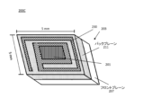
ここに記載される実施形態は、いくつかの望ましい特徴を提供する。すなわち、(1)ピラー電極アレイのオンチップ集積、(2)RF(無線周波)平面コイルとコンデンサのバックプレーン集積、(3)神経信号のハイスループット及び当該信号の記録のための低電力及び省スペース型の増幅器アレイと周辺回路、という特徴を提供する。図2B及び図2Cは、MINIデバイスのフロントプレーン及びバックプレーンを示しており、図2Aは、MINIデバイスの断面図であり、様々なデバイス層及び相互接続を示している。 The embodiments described herein provide several desirable features. (1) on-chip integration of pillar electrode arrays, (2) backplane integration of RF (radio frequency) planar coils and capacitors, (3) low power and low power consumption for high throughput of neural signals and recording of such signals. It features a space-type amplifier array and peripheral circuitry. Figures 2B and 2C show the frontplane and backplane of the MINI device, and Figure 2A is a cross-sectional view of the MINI device showing the various device layers and interconnects.
図2Aは、モノリシック集積型ニューラルインターフェース(MINI)デバイスの断面図である。本MINIデバイス200Aは、フロントプレーン層207及びバックプレーン層211を含み、これらはまとめてチップ203と呼ばれることもある。フロントプレーン層207及びバックプレーン層211は、一般にモノリシック集積され、それによりチップ203を単一のMINIデバイス200Aに形成する。RF平面コイル230は、斜線ハッチングで図示されている。フロントプレーン層207は、外面209を含み、バックプレーン層211は、外面213を含む。ここで面209及び面213は、一般に上層及び下層である。なお、ここでの「上」及び「下」という用語は、限定を意味するものではなく、参照基準として用いられているだけである。これら「上」及び「下」は「第一」及び「第二」でもよい。
FIG. 2A is a cross-sectional view of a monolithic integrated neural interface (MINI) device. The
図2Cは、図2Aに示されるMINIデバイスのバックプレーン層211の斜視図である。本MINIデバイス200Aのバックプレーン層211は、点線ハッチングで図示されているような保護層290を含んでいてもよい。この保護層290は、例えば、腐食から保護するための保護材料又はシェルである。バックプレーン層211は、図2Cにおいてよく分かるが、例えばコイル状のアルミニウムパターンを適用して形成されるRF平面コイル230を含んでおり、これは斜線ハッチングで図示されている。このアルミニウムパターンは、図2Dに関連してより詳細に論じられるが、概して、外部に露出され、無線周波(RF)信号が送受信可能となるように、バックプレーン層211に組み込まれる。
FIG. 2C is a perspective view of the
RF平面コイル230の互いに反対に位置する端部は、黒一色で図示されたシリコン貫通電極(TSV)240とインターフェースをとる。このTSV240は、図5(a)から図5(f)に関連して説明するように、フロントプレーン層207に組み込まれる。TSV240は金属を含み、その下端部、すなわち、最も幅が広い端部は、RF平面コイル230の一部に直接取付又は接着される。非限定例として、このTSV240の金属は銅(Cu)を含んでいてもよい。概して、TSV240の下端はRF平面コイル230の内面に取り付けられ、RF平面コイル230の外面は送信のため露出する。具体的には、RF平面コイル230は、一般的なU字形であってもよい。このU字型には2つの脚が含まれる。各脚の幅は、少なくともTSV240の底面の長さと同等である。各脚にはTSV240が取り付けられており、各々がクロスハッチングで図示されているIC213まで延びている。
Opposite ends of the RF
図2Bは、図2Aに示されるMINIデバイスのフロントプレーン層207の斜視図である。図2Dに関連してより詳細に説明されるが、フロントプレーン層207は、集積回路層213を含む。TSV240は、集積回路(IC)213により先端が断ち切られた形となっている。フロントプレーン層207は、その上面、すなわち外面209の一部に、クロスハッチングで図示されているIC層213が形成されている。IC層213は、第一層部253及び第二層部255を有している。第一層部253には、TSV240が直接繋がっており、これはRF平面コイル230をRF(無線)トランシーバ(TX/RX)220(図2D)に接続する。第二層部253の下の第二層部255は、概して、第一層部253よりも狭く、肩部又は第一層部253への段部を形成する。
FIG. 2B is a perspective view of the
バックプレーン層211は、縦ハッチングで図示されたコンデンサ層201を更に含む。コンデンサ層201は、第一層部253よりも短く、第二層部255よりも長い。また、コンデンサ層201の各遠位端には、一組の第二TSV242が直接繋がっている。TSV242は、概して、TSV240と同じものである。この一組のTSV242は、概して、第二(下)層部255の反対側に位置する第一(上)層部253に繋がっていてもよい。
The
IC層213の上部には、ピラー電極アレイ210が集積されている。このアレイ210の電極は、それぞれ異なるチャネルに対応している。本MINIデバイス200Aは、1000以上の電極を有し得る。
A
このMINIデバイス200Aは、以下のステップに従って製造される。まず、相補型金属酸化膜半導体(CMOS)プロセスに従った集積回路の製造を行う。次に、チップ上にピラー電極アレイを形成するためのポストCMOS処理を行う。次に、基板をエッチングして(又は基板研削/研磨技術を用いて)、基板の厚さを約50μm(一実施形態の例)に減らし、その柔軟性を上げる。次に、基板のバックプレーンにコンデンサと無線周波(RF)平面コイルをパターニングする。次に、CMOS技術及び材料加工に対応した絶縁材料(SiO2/Si3N4/SiCなど)でダイを囲むことにより、漏れの少ない障壁を作る。なお、SiCは炭化ケイ素であり、SiO2は二酸化ケイ素であり、Si3N4は窒化ケイ素である。
This
すべてのデバイスコンポーネントのモノリシック集積により、すべてのコンポーネント接続が集積回路内で行われ、外部補助機器への接続が無線周波リンクを介して行われるため、外部配線の使用が必要なくなる。露出したワイヤや接続部など、体液による腐食の影響を受けやすいものを排除し、アレイと処理コンポーネントを集積することで、埋め込み型ニューロセンサーアレイのパッケージングについての従来の要件が不要となる。チップ上でアレイとデバイスコンポーネント間の相互接続を形成することにより、本デバイスに1000個以上の電極を容易に設けることができる。 Monolithic integration of all device components eliminates the need for the use of external wiring, as all component connections are made within the integrated circuit and connections to external auxiliary equipment are made through radio frequency links. By eliminating exposed wires and connections susceptible to corrosion by bodily fluids and integrating the array and processing components, traditional packaging requirements for implantable neurosensor arrays are eliminated. By forming the interconnections between the array and device components on the chip, the device can easily have over 1000 electrodes.
図5(a)から図5(f)は、図2Aの破線ブロック241で図示されるシリコン貫通電極(TSV)を用いたMINIデバイスのRF平面コイルのバックプレーンの集積化のステップを示している。図5(a)から図5(f)のステップは、図2Aの破線ブロック241内の当該部分を形成するステップ500A、ステップ500B、ステップ500C、ステップ500D、ステップ500E、及びステップ500Fに係る断面図で表されている。RF平面コイルのバックプレーンの集積化には、シリコン貫通電極240(図2A)を用いる。RF平面コイルにおける同種層には、各ステップで同じハッチングが使われている。よって、各層ごとの参照番号は、図5(a)から図5(e)において、ほとんど一度しか使われない。また図2Aのブロック241における層のハッチングは、図5(a)から図5(e)のハッチングと一致している。
Figures 5(a) to 5(f) show the steps of the backplane integration of the RF planar coil of a MINI device using through silicon vias (TSVs) illustrated by dashed
図5(a)におけるバックプレーンの集積化のステップ500Aは、フロントプレーン層507に相当し、モノリシック集積に適した第一材料層560を形成することを含み得る。非限定例として、第一材料層560はシリコン(Si)を含んでいてもよい。この第一材料層560は、ハッチングを使わず図示されており、フロントプレーン層507及び底面562Bを含む。フロントプレーン層507の一部上には、MINIデバイス200Aのコンポーネントの集積回路540が形成されており、これはクロスハッチングで図示されている。
The
図5(b)におけるバックプレーンの集積化のステップ500Bは、バイア空洞566Bを形成するための第一材料層560におけるKOHエッチングを含み得る。バイア空洞566Bは、断面図に従うと、概して、切頂三角形の形状を有しており、第一材料層560によって境界がつけられている。フォトレジスト(PR)層564Aは、スクエアハッチングで図示されており、バイア空洞566Bの第一側に形成されている。PR層564Bは、バイア空洞566Bの反対側に、同じように形成されている。
図5(c)におけるバックプレーンの集積化のステップ500Cは、第一材料層560の底面562Bの残りの部分を酸化し、それにより、例えば、点線ハッチングで図示する酸化物層570を形成することを含み得る。酸化物層570は、二酸化ケイ素(SiO2)を含んでいてもよい。この酸化物層570は、バイア空洞566Bに対向する底面562Bの残存部分とバイア空洞566Bの壁部分とに沿って形成され、バイア空洞566Cを形成する。シリコンの酸化は、バイア空洞566Cの略切頂三角形状を維持しながら薄い酸化物層570を形成するための熱酸化を含み得る。
The
図5(d)におけるバックプレーンの集積化のステップ500Dは、バイア空洞566C(図5(c))内の銅(Cu)電着を含み得る。バイア空洞566Cは、銅がバイア空洞566Cにおける酸化物層570までの及びその間のスペースを埋め、黒一色の塗りつぶしで図示されているTSV575(すなわち、電極240)を形成する程度の量の銅(Cu)で充填される。バイア空洞566Cは、TSV575の底面576が実質的に酸化物層570と面一になるように充填されてもよい。
図5(e)におけるバックプレーンの集積化のステップ500Eは、TSV575の底面576の全長及び酸化物層570の一側面に沿って延びるように、斜線ハッチングで図示されるアルミニウムパターン585を形成することを含み得る。非限定例として、アルミニウムパターン585は、RFコイル(すなわち、RFコイル230、図2C)を形成するためのRFコイルパターン585を含み得る。
The
図5(f)におけるバックプレーンの集積化のステップ500Fは、第一材料層560に形成された残存する酸化物層570に保護層590を適用することを含み得る。RFコイルパターン585は、データ送信及び電力受信を可能とするために露出されたままでもよい。この保護層590も点線ハッチングで図示されている。保護層590の厚みにより、外バックプレーン面511を有するバックプレーン層509が形成し得る。
The
RFコイルはシミュレーション又はモデル化されており、約16.5mWの電力伝送を実現する。 The RF coil has been simulated or modeled and provides a power transfer of approximately 16.5mW.
また、基板のバックプレーン(又はフロントプレーン)に(以下に説明するようにデータ転送と発電に使用される)コンデンサとRF平面コイルを集積することにより、電力(約10mW)及びデータの同時無線伝送によるバッテリーレスな動作が可能となる。電力は、無線誘導帯電技術を用いて転送され、これにより電磁場が外部電源からRF平面コイルの1つにエネルギーを転送する。コンデンサとコイルは、従来のCMOSプロセスを用いて製造され、シリコン貫通導電電極を使用して集積回路内の他の回路素子に接続される。 Simultaneous wireless transmission of power (approximately 10 mW) and data can also be achieved by integrating capacitors and RF planar coils (used for data transfer and power generation as described below) in the backplane (or frontplane) of the board. battery-less operation is possible. Power is transferred using wireless inductive charging technology whereby an electromagnetic field transfers energy from an external power source to one of the RF planar coils. The capacitors and coils are fabricated using conventional CMOS processes and are connected to other circuit elements within the integrated circuit using through-silicon conductive electrodes.
2つのRFコイルを備えた実施形態では、第一コイルがRFリンクでデータ伝送を提供し、第二コイルがRFリンクで第二コイルに接続された外部電源に応答して電力を生成する。 In embodiments with two RF coils, the first coil provides data transmission over the RF link and the second coil generates power in response to an external power source connected to the second coil over the RF link.
データは、OOK(オンオフキーイング)変調スキームに従って約900MHzの周波数で第一RFコイルから送信されるのだが、これは、データ送信プロトコル用の他のデジタル変調スキームと比較して非常に電力効率が良い。 Data is transmitted from the first RF coil at a frequency of approximately 900 MHz according to an OOK (On-Off Keying) modulation scheme, which is very power efficient compared to other digital modulation schemes for data transmission protocols. .
一実施形態では、約10mWの電力が、外部電源によって生成された電磁場のRFカップリングによって、2.64MHz(又は、いずれの場合でも3MHz未満)の共振周波数で供給される。この電力レベルは、連邦通信委員会(FCC)に公表されているところのRF安全ガイドラインを下回っている。この安全ガイドラインでは、患者又は被験者に与える際の電力レベルを100mW/cm2に制限している。また、放射線誘発の組織損傷を最小限に抑えるために、低周波電力送信信号が使用される。これは、体液がそのような低周波信号をあまり吸収しないことが知られているからである。 In one embodiment, approximately 10 mW of power is supplied at a resonant frequency of 2.64 MHz (or in any case less than 3 MHz) by RF coupling of an electromagnetic field generated by an external power source. This power level is below the RF safety guidelines published by the Federal Communications Commission (FCC). This safety guideline limits power levels when applied to a patient or subject to 100 mW/cm 2 . Also, low frequency power transmission signals are used to minimize radiation-induced tissue damage. This is because body fluids are known to absorb such low frequency signals poorly.
以下の表1は、ニューラルインターフェースデバイス内の各コンポーネントのおおよその電力消費範囲を示している。

外部電源880(図8Aから8B)からのRF電力信号は、第二コイルにおいてAC信号を生成する。第二コイルとシリコン基板の緊密なカップリングは、電力伝送を減衰させる寄生容量を引き起こす可能性があり、そのため第二コイルはデバイスのバックプレーンに配置される。 An RF power signal from an external power supply 880 (FIGS. 8A-8B) produces an AC signal in the second coil. The tight coupling between the second coil and the silicon substrate can cause parasitic capacitance that attenuates power transfer, so the second coil is placed on the backplane of the device.
電力伝送効率は、第二コイル及び外部電源間の分離距離が約1.5cmの場合において最適化される。直流(DC)に変換した後、生じた信号がフィルター処理され、出力電圧が電圧レギュレーターによって設定される。 Power transfer efficiency is optimized when the separation distance between the second coil and the external power source is approximately 1.5 cm. After conversion to direct current (DC), the resulting signal is filtered and the output voltage is set by a voltage regulator.
変換されたDC信号をフィルタリングするためには、かなり大きいコンデンサが必要となる。適切なフィルタリング及び後続する電圧レギュレーションのための1μFもの大きな静電容量を達成するため、約25mm2の面積を占める金属-絶縁体-金属(MiM)コンデンサが基板のバックプレーンに配置される。 A fairly large capacitor is required to filter the converted DC signal. To achieve a capacitance as large as 1 μF for proper filtering and subsequent voltage regulation, metal-insulator-metal (MiM) capacitors occupying an area of approximately 25 mm 2 are placed on the backplane of the substrate.
送電コイル及びコンデンサは、図2Aでよく図示されているが、干渉効果を回避するため、保護層によって分離された基板の異なる層に配置される。 The transmitting coils and capacitors, best illustrated in FIG. 2A, are placed on different layers of the substrate separated by protective layers to avoid interference effects.
他の実施形態では、バッテリーをモノリシックデバイスに組み込むことができ、それにより、デバイスのコンポーネントにリアルタイム電力を供給するためのRF電力カップリングが不要となる。RF電力カップリングは、バッテリーを充電するために使用されることが好ましい。 In other embodiments, the battery can be integrated into the monolithic device, thereby eliminating the need for RF power coupling to provide real-time power to the device's components. RF power coupling is preferably used to charge the battery.
また、他の実施形態では、電力伝送を増大させるのに特に有利なことであるが、シリコン基板の代わりにシリコンオンインシュレータ(SOI)基板が使用される。この実施形態は、シリコンバルクと平面コイルとの間の距離を長くすることで、寄生容量を低下させるものである。 Also, in other embodiments, silicon-on-insulator (SOI) substrates are used instead of silicon substrates, which is particularly advantageous for increasing power transfer. This embodiment reduces the parasitic capacitance by increasing the distance between the silicon bulk and the planar coil.
また、他の実施形態では、コイルの直列抵抗を低減しながら、コイルのインダクタンス及び品質係数が増加するように、基板サイズを大きくし、25mm2以上にする。大きい基板は、大きいコイルの製造を可能にする。いずれの場合でも、MINIデバイスは、現在の最先端BCIシステムのサイズより小さいままとしてもよく、そのサイズは、アレイ内に約100の電極を備えた状態で約68.64cm3である。 Also, in other embodiments, the substrate size is increased to 25 mm 2 or more to increase the inductance and quality factor of the coil while reducing the series resistance of the coil. A large substrate allows the manufacture of large coils. In any case, the MINI device may remain smaller than the size of current state-of-the-art BCI systems, which is approximately 68.64 cm 3 with approximately 100 electrodes in the array.
薄い基板は、約0.0125cm3のMINIデバイス体積を提供し、これは現在の最先端デバイス、すなわち、68.64cm3より大幅に小さい。50μmという厚さは、頭蓋骨の下に移植するための基板の柔軟性を提供する。また、すべてのコンポーネントをチップに統合することで、外科的インプラント処置が簡素化される。 The thin substrate provides a MINI device volume of approximately 0.0125 cm 3 , which is significantly smaller than the current state-of-the-art device, namely 68.64 cm 3 . A thickness of 50 μm provides substrate flexibility for implantation under the skull. Also, integrating all components into the chip simplifies the surgical implant procedure.
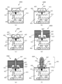
図3(a)から図3(d)は、MINIデバイスにおけるオンチップピラー電極アレイのためのオンチップ金電極の無誘導電着に関連するステップを示す。図3(a)におけるオンチップ金電極を形成するための無誘導電着のステップは、CMOSダイ305Aに重ねたアルミニウム(Al)層に開口部315Aを形成するステップ300Aを含む。ピラー310Aは、CMOSダイ305A上に示されおり、電極のオンチップ集積に使用される。図3(b)におけるステップ300Bは、セクション315Bのアルミニウムを、CMOSダイ305B上のパッド310Bを介してエッチングすることを含む。図3(c)におけるステップ300Cでは、電着によりパッドセクション310Cをニッケル315Cでメッキする。ニッケルは、CMOSダイ305Cには及ばせない。図3(d)におけるステップ300Dでは、セクション310Dにおいて金315Dをニッケル層に電気めっきする。金メッキは、CMOSダイ305Dには及ばせない。
Figures 3(a) to 3(d) show the steps involved in non-inductive electrodeposition of on-chip gold electrodes for an on-chip pillar electrode array in a MINI device. The step of non-inductive electrodeposition to form the on-chip gold electrodes in FIG. 3(a) includes
オンチップ電極アレイ210(図2A)は、電着技術を用いて形成される。電着は等方性堆積プロセスであるため、パターン化フォトレジスト(PR)層で電着プロセスをガイドすることにより、高アスペクト比のピラー電極が製造される。 An on-chip electrode array 210 (FIG. 2A) is formed using electrodeposition techniques. Since electrodeposition is an isotropic deposition process, high aspect ratio pillar electrodes are produced by guiding the electrodeposition process with a patterned photoresist (PR) layer.
図4(a)から図4(f)は、図4(f)に最も分かりやすく記載されているタングステンコアを有するピラー電極455を製造するための誘導電着の段階図400A、400B、400C、400D、400E及び400Fである。なお、同様のコンポーネントには同じ参照番号が付してある。ただし、コンポーネントに変化が生じた場合、その参照番号にはダッシュ記号又はダブルダッシュ記号が付くこととなる。図4(a)から図4(f)は同様の参照番号を有しているが、1つの図で言及された参照番号は、必要でない限り、後の図の説明において再び言及されることはない。ピラー電極アレイの望ましい特性の1つは、外科手術中及び移植後における脳表面により引き起こされるせん断応力に対する高い構造抵抗である。したがって、実施形態によっては、各ピラーは高いヤング率を示さなければならない。一実施形態では、各電極は、タングステンコア及び金の外面を有し、これにより比較的堅いピラー及び電極となる。アレイ210の実施形態は、移植部位に応じて異なる形状及び長さとなる。各ピラーは、ヒトの硬膜又は軟膜を貫通するために少なくとも50μmの長さであることが好ましい。
Figures 4(a) through 4(f) illustrate stages of
図4(a)におけるステップ400Aは、図2Aから図2Dに関連して説明されたような集積回路(IC)413が埋め込まれた又は集積されたCMOSダイ403の形成に関連して説明される。IC413は、例示を目的として、破線ボックスの層で図示されている。CMOSダイ403は、例えば、シリコンで作られてもよい。導電性リード411は、CMOSダイ403に埋め込まれ、IC413に接続される。なお、他のリードが設けられてもよい。
CMOSダイ403は、その上面に、導電性リード411に電気的に接続されるアルミニウム(AL)パッド415又はストリップ(点線ハッチングで図示)が埋め込まれている。導電性リード411は、Alパッド415より下に位置する。Alパッド415又はストリップは、第一の高さと幅を有している。ALパッド415は、CMOSダイ403における二点鎖線で図示される上面405の上にあり、ピラー435の真下に埋め込まれる。ピラー435は、例えば二酸化シリコン(SiO2)で作られた酸化物層407がCMOSダイ403の上面405及びAlパッド415の上面に適用されることで、形成される。ALパッド415がCMOSダイ403の上面の上にあるので、このピラー345として示される隆起部分が形成される。
The CMOS die 403 is embedded on its top surface with aluminum (AL)
図4(b)におけるステップ400Bは、ピラー435’にAlパッド415の上面まで延びるオープンチャネル440又は経路を形成するように酸化物層407をエッチングすることを含む。図4(c)におけるステップ400Cは、AIパッド415’の物質をピラー435’のチャネル440’を通して除去することで、AIパッド415’がある量だけ低減し、電極支持ベース(ESB)キャビティ425が形成されるようにエッチングすることを含む。ESBキャビティ425は、その幅が、Alパッド415の幅と同じであってもよいが、開放チャネル440’の幅よりは大きくあるべきである。
Step 400B in FIG. 4(b) involves etching the
図4(d)におけるステップ400Dは、酸化物層407及び対応するピラー435’の上に、水平ハッチングで図示されたパターン化フォトレジスト(PR)層442を形成することを含む。フォトレジスト層442の高さは、電極に必要な高さの関数である。PR層442は、オープンチャネル440’’を有する。したがって、オープンチャネルは、ESBキャビティ425までの明確な経路が形成されるように、ピラー435’内に形成されエッチング後のALパッド415’に至るオープンチャネル440’と、PR層442内のオープンチャネル440’’との両方を含む。実施形態によっては、オープンチャネル440’及びオープンチャネル440”は、ESB空洞425内を除いて同じ直径を含み得る。
図4(e)におけるステップ400Eは、ESBキャビティ425内に斜めハッチングで図示されている電極導電性コアベース445を形成すること、及び開放チャネル440’の残り及び開放チャネル400’’に沿って、斜めハッチングで図示されている導電性電極コア447を形成することを含む。ステップ400Eは、ESBキャビティ425とオープンチャネル440’及び440”を導電性金属で電気めっきし、キャビティ425とチャネル400’及び400’’の両方を充填して、一体型電極ベース445によって支持された電極コア447を含み得る固体単一電極コア構造を形成することを含んでいてもよい。実施形態によっては、電気めっきは、PR層442の上面443より上に電極コア447を延ばすことを含んでいてもよい。また、実施形態によっては、導電性金属は、タングステン又は他の構造的に強い材料を含む。
図4(f)におけるステップ400Fは、PR層442を除去し、ピラー435’の上方に延びる導電性電極コア447を、スクエアハッチングで図示される金(Au)層450で封入及び完全に包含することを含む。金層450は、ピラー435’まで伸びる。この金層450は導電性電極コア447の先端も封入する。導電性電極455は、金層450、導電性電極コア447、及びCMOSダイ403内の導電性リード411と電気通信する電極ベース445を含むこととなる。
非限定例において、金層450は、電極コア447の露出された外周面及び周囲に電気めっきされる。
In a non-limiting example,
他の実施形態では、ピラー構造アレイは、平面電極アレイに置き換えられる。後者のアレイを使用するデバイスは、ピラー構造の場合のように硬膜上ではなく、硬膜下に埋め込む必要がある。これは、平面アレイ電極が硬膜の厚い膜を貫通できないからである。 In other embodiments, the pillar structure array is replaced with a planar electrode array. Devices using the latter array must be implanted subdurally rather than epidurally as in the case of pillar structures. This is because planar array electrodes cannot penetrate the thick membrane of the dura mater.
図2Dは、MINIデバイス200Dの主要なコンポーネントを示すシステムブロック図である。実施形態によっては、電極アレイ210の各電極からの信号は、1対1対応で、増幅器アレイ212における対応する増幅器によって増幅される。これら複数の電極信号は、例えば、マルチプレクサ(MUX)214を使用して(10MS/sで時分割多元接続(TDMA)アプローチを使用するなどして)多重化され、120Mビット/秒でアナログ-デジタル変換器(ADC)216においてデジタル形式に変換される。これらのデジタル信号は、プロセッサ218でデータ圧縮などの処理を施される。プロセッサ218は、デジタル信号プロセッサでもよい。プロセッサ218からの信号は、無線周波(RF)トランシーバ(TX/RX)220に送られてもよく、そこでRF信号が生成される。RF信号は、コイル230を介して離れた場所にある外部信号分析装置に無線送信され、記録及び分析が行われる。
FIG. 2D is a system block diagram showing the major components of
TDMA多重化は、すべての積分期間をずらし、その結果、1つの増幅器からのデータが読み取られている間に、他の増幅器が感知された情報を積分し続ける。この多重化スキームは、信号対雑音比(SNR)を最大化し、回路複雑度を最小化する。 TDMA multiplexing staggers all integration periods so that while data from one amplifier is being read, other amplifiers continue to integrate sensed information. This multiplexing scheme maximizes the signal-to-noise ratio (SNR) and minimizes circuit complexity.
これも図2Dに示されていることだが、電力はRFリンクを介してMINIデバイス200Dに供給され、AC-DCコンバーター222によって直流(DC)に変換され、電圧レギュレーター224によって適切な電圧に調整され、そしてデバイスコンポーネントに供給される。なお、ACとは交流を意味する。
Also shown in FIG. 2D, power is supplied to
本発明のモノリシックニューラルセンサには、様々な増幅器構成を用いること可能である。一実施形態によれば、MINIデバイス200Dは、アレイ210の各電極に1つの低雑音増幅器(LNA)アレイ212を備える。一般に、これはより電力効率の良い設計であるが、増幅器を収容するためにより大きな面積を必要とする。一実施形態では、1000-増幅器アレイ210は、10kS/s(キロサンプル/秒)のサンプリングレート及び約5μVRMSのノイズレベルで約10mm2の面積を占める。この設計は拡張性があるため、1000のチャネル、1000の増幅器、1000の電極を超えることも出来る。
A variety of amplifier configurations can be used with the monolithic neural sensor of the present invention. According to one embodiment,
図6Aは、固有のSINCフィルターを備えた神経記録回路600を示す。デバイス内の増幅器は、積分期間に基づいたSINCフィルターを使用してエイリアシングノイズの内的除去を行う。このフィルタリングにより、全体的な信号対雑音比(SNR)が向上する。この増幅器は、コンデンサCint617を有するポテンショスタットを用いる。電極610で神経活動(Vneural)によって生成された電位により、コンデンサCE619で電位降下が発生し、結果として生じた電流は、コンデンサCint617で積分され、トランジスタ603のソースで電圧(Vreadout)として一定期間ごとに表示される。電流源613は、トランジスタ601のソースに結合する電流(Ibaseline)を提供する。トランジスタ601及び602のドレインは結合し、トランジスタ603のゲートに接続される。スイッチSW1は、コンデンサCint617への経路、及びトランジスタ601及び602のドレインとトランジスタ603のゲートとの間の経路に接続される。また、スイッチSW1は、コンデンサCint617への経路を開閉する。
FIG. 6A shows a
トランジスタ601は、そのゲートが、入力Vref及びIbaselineを受けつける演算増幅器(OPA)611に接続される。また、電極610は、コンデンサCE619を介して、増幅器(OPA)611の入力に接続される。
表示電圧は、以下の式から分かるように、Vneuralを表す。

正弦波周波数でVneuralを効果的に「再サンプリング」するために、高周波正弦波がVrefに適用される。その周波数では、入力コンデンサ(sCE)のインピーダンスは一定であるため、電圧ゲインの周波数依存が排除される。

一実施形態では、電圧利得は、利得パラメータをScarrier=2×π×5kHz、CE=2pF、Cint=63fF、そしてtint=100μsに設定することによって、100に調整される。ノイズレベルは、100×100μm2のサイズ及び10kS/sのサンプリングレートで約5μVRMS以下である。したがって、一実施形態では、増幅器アレイは、タイミング回路やマルチプレクサ回路などの周辺回路を除き、3.2×3.2mm2である。 In one embodiment, the voltage gain is adjusted to 100 by setting the gain parameters to S carrier =2×π×5 kHz, C E =2 pF, C int =63 fF, and t int =100 μs. The noise level is below about 5 μV RMS with a size of 100×100 μm 2 and a sampling rate of 10 kS/s. Thus, in one embodiment, the amplifier array is 3.2×3.2 mm 2 excluding peripheral circuits such as timing circuits and multiplexer circuits.
他の実施形態によれば、増幅器は、電圧利得における周波数成分を無効化するコンデンサフィードバック増幅器を備える。こういった増幅器は、当技術分野では既知である。 According to another embodiment, the amplifier comprises a capacitor feedback amplifier that nulls frequency components in the voltage gain. Such amplifiers are known in the art.
図6Bは、エイリアシングノイズの一因となる高周波を減衰させる固有フィルターのグラフ表示を示している。集積システムの固有フィルターは、エイリアシングノイズの原因となる高周波を減衰させる。カットオフ周波数は、SINCフィルターで予測されるように、10kS/sで4.4kHz以下である。 FIG. 6B shows a graphical representation of an eigenfilter that attenuates high frequencies that contribute to aliasing noise. Eigenfilters in integrated systems attenuate high frequencies that cause aliasing noise. The cutoff frequency is below 4.4 kHz at 10 kS/s, as predicted by the SINC filter.
図7Aは、1000チャネル増幅器アレイ712及び神経記録回路700の一部を示す。図7Aにおける1000チャネル増幅器アレイ712の各増幅器は、電極を介した神経記録で使用するピコアンペア増幅器でもよい。この増幅器アレイ712の一部712Aは拡張されている。
FIG. 7A shows a portion of the 1000
図7Bは、最先端の電気生理学増幅器Axopatch200Bと比較した場合における、図7Aの設計されたCMOS増幅器のノイズスペクトル密度のグラフ表示750を示す。
FIG. 7B shows a
図8Aは、第一MINIシステム800Aを示す。本MINIシステム800Aは、図示されているバックプレーン211を有するMINIデバイス200Cと、リモートシステム850Aとを含む。MINIデバイス200Cは、対象者Sの脳870に埋め込まれた状態で示されている。このMINIデバイス200Cは、図19に関連して説明するコンピューターシステムなどのリモートアナライザ875Aと通信するように構成されている。外部電源880は、MINIデバイス200Cに電力信号を提供するように構成されている。リモートシステム850Aは、これらリモートアナライザ875A及び外部電源880を含み得る。リモートシステム850Aは、1つのデバイスで構成されていてもよいし、2つの別個のデバイスで構成されていてもよい。リモートシステム850AとMINIデバイス200Cとの間の距離は、データ信号及び電力信号のワイヤレス通信の範囲によって制限され得る。いくつかの実施形態における通信では、遠隔測定法を使う。システム800Aは、例えば、MINIデバイス200Cが埋め込まれた被験者Sからモデルデータをとるために使用されてもよい。
FIG. 8A shows a
図8Bは、人工装具860と共に使用する第二MINIシステム800Bを示す。第二MINIシステム800Bは、外部電源880と人工装具860に取り付けられた又は埋め込まれた計算装置875Bとを含み得る遠隔システム850Bを含む。計算装置875Bは、プロセッサ、メモリ、メモリに記録された命令、及び/又は図19のコンピューターシステムに関連して説明される1つ又は複数の他のコンポーネントを含み得る。人工装具860は、MINIデバイス200Cからのセンサー神経データに基づいて制御され得る1つ以上のアクチュエータ865を含んでもよく、リモートシステム850B及びMINIデバイス200Cは、それらの間の専用通信のためにペアリングされ得る。実施形態によっては、MINIデバイス200Cは、リモートシステム850A及び850Bと通信することが可能であってもよい。
FIG. 8B shows a
図9(a)から図9(c)は、金電着を用いたオンチップ電極アレイの製造のステップを示す。図9(a)におけるステップ900Aは、CMOSチップ上での直接電気めっきプロトコルを使用することを含み得る。図9(a)に最もよく示されているように、最初に、上部金属層907が、アルミニウムエッチングによって除去される。この上部金属層907は、アルミニウム及び銅を含み得る。非限定例として、ステップ900Aにウェットエッチング方式を用いてもよい。
Figures 9(a) to 9(c) show the steps in the fabrication of an on-chip electrode array using gold electrodeposition.
図9(b)のステップ900Bは、ニッケル(Ni)層917を形成するためのニッケル(Ni)めっきを含み得る。例えば、Ni層は、電着を使用して付してもよい。図9(c)におけるステップ900Cは、Ni層を金(Au)でめっきして金層927を形成することを含み得る。電気めっきのため、電流ミラー回路に基づく内部電流源回路がCMOS集積回路内に設計されており、めっきプロセスを通じて一定の電流が引き出される。結果的に、図9(c)に示すように、自己整合電極アレイ210が作られた。
図9(d)は、図9(a)から図9(c)のステップを使用して作成された電極に従ったオンチップ電気めっき電極を用いたドーパミン測定のグラフ表示950を示す。ここで、図9(a)から図9(c)で作成されたオンチップ記録のための電気めっき電極の品質のテストが行われた。図9(a)から図9(c)の電極をテストするため、500μMのドーパミン溶液がCMOSチップの表面に塗布された。これにより、図9(d)に示すように首尾よく記録が得られた。ドーパミン測定は、これらの電極が意図されている活動電位測定を直接反映するものではなく、製造プロセスの安定性と有効性をテストするものである。
FIG. 9(d) shows a
図10(a)~図10(b)は、電気めっき電極1045を、上面及びオンチップ電極を切断する集束イオンビーム(FIB)により得られた断面から見た場合の画像1000A及び1000Bを示している。FIBにより、ある角度からの走査型電子顕微鏡(SEM)画像をキャプチャして、オンチップ電極1045の断面を示すことができるのだが、電気めっきアプローチのマイナス面が観察された。本明細書に記載のMINIデバイスを製造するためのモノリシック集積方法をテストする際、電極の信頼性とロバスト性が追跡された。図9(d)に示した測定成功をよそに、図9(a)から図9(c)におけるアプローチのテストには、安定性と信頼性が欠けていた。図10(b)に関して、ピラー1035にピラー電極1045を作成するための電気めっきプロセスの画像1000Bには、不安定性を引き起こすことが示された。図10(b)に示されるように、電極1045の電気メッキ金属とMINIデバイスのCMOSチップ又はダイ1003の間に小さなボイド1066(サブミクロン)がはっきりと見える。これは、電解液がボイドに漏れてMINIデバイスのCMOSチップ又はダイ1003に損傷を引き起こす可能性があるため、望ましくない。
FIGS. 10(a)-10(b)
図12(a)から図12(c)に関連して説明されるように、ここに記載されるポストCMOS手順は、標準的なフォトリソグラフィープロセスを使用して電極アレイ210(図2D)のオンチップ電極1045を製造するために使用されてもよい。さらに、ポストCMOS手順を使用して、CMOSチップ1003上に1024個のオンチップ金電極を作製することができ、これは、図13Aから図13Bに関連して説明するように、活動電位測定に使用することができる。図12(a)~図12(c)は、平面電極及びSU-8ウェル1219Cのオンチップ集積のためのポストCMOS処理ステップに係る断面図を示す。CMOSチップの最上金属層は、ほとんどの従来のCMOSプロセスにおいてアルミニウム-銅合金だが、電解液に対するアルミニウムの反応性が高いため、バイオセンシングには適切ではない。これにより、電気生理学的記録でオフセットが大きくなり、ショットノイズが高くなるだけでなく、漏水によりチップが損傷する可能性も出てくる。金やプラチナなどの分極性電極材料は、反応性が低いため、電気生理学的記録により適している。図11(a)から図11(c)は、図12(a)~図12(c)で説明されるような平面電極及びSU-8ウェルのオンチップ集積のためのポストCMOS処理のステップに係る上面図を示す。そのため、図11(a)から図11(c)を図12(a)から図12(c)と併せて説明する。ここで、図11(a)から図11(c)のいくつかの参照番号は、これらの図に示されており、対応する参照番号は、同じ要素を参照しているが、これらの図の参照番号のいくつかは、図11(a)から図11(c)には示されていない。
12(a)-12(c), the post-CMOS procedure described herein turns on the electrode array 210 (FIG. 2D) using standard photolithographic processes. It may be used to fabricate
図11(a)及び図12(a)は、CMOSダイ1203であって、その材料上に酸化物で作られた第一層1207を重ねた又は形成したものを作成することを含むステップ1100A/1200Aを示す。ピラー1235は、各電極に形成される。パッド1235の中心は、アルミニウム又はアルミニウムと銅の合金を含み得る第二(金属)層1215に向けて開放されている。第二層1215は、パッド1235及び第一(酸化物)層1207の形成前に、CMOSダイ1203上に堆積させてもよい。図11(b)及び図12(b)は、図12(a)のCMOSダイが、ピラー1235及び第一(酸化物)層1207の一部の上に重ねられた第3層1217Bを有することを含むステップ1100B/1200Bを示す。第一層1207(図12(a))の一部1212は、この重ねられた第二層1217Bを含まない。第二層1217Bは、金(Au)を含む。
Figures 11(a) and 12(a) illustrate
図11(c)及び図12(c)は、図12(b)のCMOSダイ1203が、リフトオフプロセスを用いてパターン化された第3層(金層)を有することを含むステップ1100C/1200Cを示しており、リフトオフプロセスの後には、第3層の一部及び第一層1207の一部1212の上に重ねられる第4層1219Cの製造が続く。第4層1219Cは、SU-8層であり得る。パッド内のチャネルも第4層1219Cで満たされる。ウェル1221Cは、SU-8層の一部に形成され、これも第3層1217C上に重なる。このウェル1221Cは、例えば、SU-8層1219Cを貫通し、金で作られた第3層1217Cに達する開口部である。
Figures 11(c) and 12(c) illustrate
図13Aは、様々なトレース幅にわたる一定結合係数のグラフ表示1300Aを示しており、図13Bは、様々なスパイラル巻数にわたる一定結合係数のグラフ表示1300Bを示している。RF平面コイルは、無線電力伝達を提供し得る。また、このRF平面コイルは、角型スパイラルコイルを含み得る。ここでは、ANSYS高周波構造シミュレータ(HFSS)を用いて調査が行われた。誘導性リンクの電力伝達効率は、結合係数、インダクタンス、及び直列抵抗に依存する。そして、結合係数(k)は、距離、外径、内径、トレース幅(図13A)、間隔、巻数(図13B)の関数であることが知られている。パラメータの複雑な依存関係のため、2つのコイルの最適な組み合わせを決定することは困難な作業である。この分析において、発明者は、角型スパイラルコイルの結合係数に影響を与える多くのパラメータのうち、送信(TX)コイルと受信(RX)コイルの外径(OD)と内径(ID)が考慮すべき重要な要素であることを確認した。ODとIDが一定に保たれている限り、間隔、トレース幅、及び巻数は、結合係数にほとんど影響しない(図13A及び図13B)。この観察は、丸形スパイラルコイルの観察と一致している。図14Aは、rxID/rxODまでの間隔(z)の関数としての角型スパイラルコイルの最適な幾何学的値のグラフ表示1400Aを示している。この観測を使い、広範囲のIDとODに基づく最適な結合係数をHFSSシミュレーションに基づいて示す。このデータを使用して、最適な角型スパイラルコイルのためのコイル設計方法とMatlabマクロが開発された。Matlabマクロは、製造能力による設計制約に関する入力パラメータを必要とし、これらのパラメータを使用して、受信コイルと送信コイルのデザインのすべての可能な組み合わせを数秒でスキャンし、最高の電力伝達効率をもたらす設計パラメータの組み合わせをアウトプットする。コイルは、標準のフォトリソグラフィを使用して製造してもよく、それで電力伝達効率を測定する。
FIG. 13A shows a
図14Bは、間隔(z)からtxOD/rxODまでの関数としての角形スパイラルコイルの最適な幾何学的値のグラフ表示1400Bを示す。図14Cは、txID/txODまでの間隔(z)の関数としての角形スパイラルコイルの最適な幾何学的値のグラフ表示1400Cを示す。大きく黒い点は、特定のzで達成可能な最高のk(kmax)を表しており、各黒点がラインと交差する。各ラインには、0.9kmaxを超える幾何学的値を示す第一小点グループ及び0.9kmax未満の第二小点グループが存在する。0.9kmax未満の小点は、各ラインの上下のポイントに存在する。図14Aにおいて、第一ラインの0.6以上の点は、第二小点グループである。第一ラインの残りの点は、第一小点グループである。第二ラインにおいて、同ラインの上3点と最後の7点は、第二小点グループの一部である。残りの小点は、第一小点グループの一部である。最大及び最小ポイントにおける各グラフは、第二小点グループの一つ以上の点を含む。
FIG. 14B shows a
図15Aは、標準的な0.35μmのCMOSプロセスで設計された1024チャネルのブレインマシーンインターフェースチップを含むMINIデバイス1500Aを示している。増幅器及び電極ペアアレイ1566は、32×32として示されている。ただし、その拡張性により、より多くの電極/増幅器のペアを追加できる。CMOSプロセスとMINIデバイス1500Aは、標準的な0.35μmのCMOSプロセスを用いて製造できる。MINIデバイス1500Aは、1000-チャネルモノリシックブレインマシーンインターフェースデバイスとして構成し得る。チップは、1566という参照番号が付された1024個のオンチップ増幅器及び1024個のオンチップ電極のペア、オンチップ無線電力コイル1530、オンチップ無線データコイル1531、送信機、電圧調整器、及び整流器を含み得る。
FIG. 15A shows a
図15Bは、図15AのMINIデバイス1500Aのための増幅器及び電極ペアアレイ1566を示している。図15Bに示される各増幅器及び電極ペアアレイ1566は、約70μm×70μmの面積を占めてもよく、チップ全体が約3.8mm×3.8mmを占める。ここではグランドGNDとクロックCLKが示されている。
FIG. 15B shows an amplifier and
図16Aは、圧縮神経記録のためのデルタ変調器1600Aの概略図を示し、この概略図は、プリセット閾値を超える又は下回る電圧の変化が検出されたときに導線1633にリセットパルスをもたらす2つのコンパレーター1623及び1625を含む。典型的な神経記録システムは、電圧増幅器とアナログデジタルコンバーター(ADC)で構成されている。神経電位が電圧増幅器を用いて増幅され、ADCがデータ処理及び送信のためにアナログ値をデジタル値に変換する。ただし、この方法では、ADCにより消費電力が大きくなり、加えてADCのサイズにより面積が大きく使われるのだが、どちらも低電力のインプラントデバイスには好ましくない。典型的な神経記録システムとは異なり、上記MINIデバイスは、実施形態によっては、ADCを必要とせずに高いデータ圧縮能力を有するデルタ変調器を含み得る。
FIG. 16A shows a schematic diagram of a
電極1610で検出された神経信号Vneuronは、入力コンデンサ(C2)1641を介して入力電流Ineuronに生成される。この電流はフィードバックコンデンサ(C1)1639を介して積分され、出力電圧Voutを変化させる。この出力電圧Voutは、下記式で表すことが出来る。

図16Bは、幅厚デジタルパルス(すなわち、パルス1664、1668、及び1670)を引き起こすVref(範囲1652内)+ ΔVth(範囲1658内)を超える電圧Voutの電圧上昇、及び幅薄デジタルパルス(すなわち、パルス1662、1666、及び1672)を引き起こすVref-ΔVthを下回る電圧降下のグラフ表示1600Bを示す。範囲1652と1658は破線1656で区切られている。図16Bには、パルス列1660で表される6サイクルの例が示されている。-VneuronによるVref+ΔVthを超えるVoutの電圧上昇は、幅圧パルス(1ビット×2)をもたらす。同様に、+ΔVneuronによるVref-ΔVthを下回る電圧降下は、幅薄パルス(1ビット×1)をもたらす。パルス幅は、記録されたΔVneuronの極性を識別するために後で使用できる。閾値条件(Vref±ΔVth)のいずれかが満たされると、AND(1627)ロジックによりコンデンサ(C1)1639をリセットするようパルスが高くなり、Vout=Vneg=Vrefを確立して新しい検出サイクルを再開する。
FIG. 16B shows the voltage rise in voltage V out beyond V ref (in range 1652) + ΔV th (in range 1658) that causes a thick digital pulse (i.e.,
図17Aは、デルタ変調器及び従来の神経記録システムに基づく神経信号サンプリング1700Aを示している。ここで、スパイクは、1mVの神経スパイクの例であり、三角(▲)は、デルタ変調器がサンプリングする場所を示し、バツ(×)は、従来のシステムがサンプリングする場所を示している。デルタ変調器のシミュレーション研究を図17Aから図17Cに示す。この研究では、1mVのピークを持つ活動電位例が、デルタ変調器と従来の神経記録システムに入力される。通常、皮質脳波記録法(ECoG)の測定では、30μV-5mVの神経スパイクが生じる。従来の神経記録システムは、図17Aのバツ印(×)で示されるように、固定レートで神経信号をサンプリングする。デルタ変調器は電圧変化にのみ敏感であるため、ノイズによる微量なマイクロボルトの変動を測定しない。図17Aでは、デルタ変調器のサンプリングが三角(▲)として示されている。図17Bに示すように、各デルタ変調器のサンプルは、パルス列で1つ又は2つの1ビットパルスを即座に生成する。
FIG. 17A shows
図17Bは、デルタ変調器のサンプルに基づく神経信号のサンプリングに基づいたパルス列1700Bを示す。この例では、デルタ変調器は57ビットのデータ又はパルス列を生成する。これは元の信号を高いマッチング精度で再構成するのに使用できる。図17Cは、デルタ変調器のサンプルに基づく神経信号1700Cの再構成を示す。図17Dは、定速サンプリングに基づく神経信号1700Dの再構成を示す。図からわかるように、信号1700Cと1700Dはほぼ一致している。ただし、通常の定速サンプリングでは、12ビットADCを使用すると仮定すると、588ビットのデータに対応する49サンプルが生成される。これはデータ圧縮の10倍以上である。各方法からの信号再構成の比較では、デルタ変調器からのスパイクにおいて元のグレー信号と同等又はより類似していることが分かる。したがって、デルタ変調器を使用すると、ひずみのない神経信号圧縮検知が実現できる。
FIG. 17B shows a
図18は、シンプルな演算増幅器(OPA)1809及び2つの疑似コンパレーター1839A及び1839Bを用いるデルタ変調器1800のコア回路概略図を示す。このデルタ変調器1800の回路デザインは、2つの条件を満たし得る。第一の条件は、デルタ変調器1800のサイズに関係し、小さい領域に収まるようにすることである。第二の条件が含むのは、内蔵バッテリーがなくMINIデバイスをワイヤレスで動作させる場合の最小電力消費である。このようなことから、MINIデバイスは、シンプルな演算増幅器(OPA)1809及び2つの疑似コンパレーター1839A及び1839Bを用いてもよい。
FIG. 18 shows a core circuit schematic of a
複雑な演算増幅器(OPA)のデザインでは、高いゲイン及び帯域幅を有することができるが、電力消費が高く、大きい実装面積を必要とする。OPA1809の反転側と非反転側の間のミスマッチを最小限に抑えるには、入力トランジスタと負荷トランジスタに比較的大きな領域を与えることが望ましい場合がある。200V/Vまでのゲインと50kHzまでの帯域幅は、シンプルなOPAデザインで簡単に実現できるため、MINIデバイスは、5トランジスタベースのOPAを用いて、M1からM4として図示される大きな領域をトランジスタ専用にしてもよい。実施形態によっては、増幅器1819及び1829のような2段増幅器を用いて、全体的なゲインを5,000から16,000V/Vの間に設定することができる。シリコン領域を効率的に使用するため、半共用OPA1809を使用してもよい。ノード1822は、Vneuronとして図示される神経又は神経系の信号を受信する。トランジスタM1からM17は、MOSFETタイプのトランジスタでもよい。
Complex operational amplifier (OPA) designs can have high gain and bandwidth, but consume high power and require large footprints. To minimize mismatch between the inverting and non-inverting sides of
増幅器1819及び増幅器1829は、増幅器(OPA)1809の非反転側を共有し、この増幅器(OPA)1809は、M1、M2、及びM9として図示される複数のトランジスタを含み得る。増幅器1819は第一段増幅器であり、コンデンサC10及びC11を備えたトランジスタM3、M4及びM7を含み得る。コンデンサC10は、ノードVout1及びトランジスタM4のゲートに接続される。トランジスタM3及びM4のドレインは、共にノードVout1に接続される。トランジスタM7のドレインは、ノードVout1に接続される。トランジスタM7及びM8のソースには、電圧Vrefがかかる。トランジスタM7及びM8のゲートは、パルス信号を受信する。トランジスタM2及びM9のゲートには、それぞれ電圧Vref及びVbnがかかる。バイアス電圧Vbnは約0.5Vでよく、チップ内部で設定してもよい。トランジスタM2のソース及びトランジスタM9のドレインは互いに接続され、そしてトランジスタM4及びM6のソースに接続される。
増幅器1829は、トランジスタM5、M6並びにM8及びコンデンサC12並びにC13を有する第二段増幅器である。トランジスタM5及びM3は、そのゲートがトランジスタM1のゲートに繋がる。増幅器1819及び1829は、通常、互いにミラー化される。しかしながら、ノード1822は、コンデンサC11を介してトランジスタM4のゲートに接続される。またトランジスタM3、M4及びM7のドレインにおける電圧Vout1のノードもノード1832に接続されてもよい。
Vout2のノードは、トランジスタM5、M6及びM8のドレインに繋がる。コンデンサC12は、Vout2ノードとトランジスタM6のゲートに接続される。電圧Vout2は、疑似コンパレーター1839A及び1839BのトランジスタM10及びM15のゲートにそれぞれ接続される。 The V out2 node is connected to the drains of transistors M5, M6 and M8. A capacitor C12 is connected to the V out2 node and the gate of transistor M6. Voltage V out2 is connected to the gates of transistors M10 and M15 of pseudo-comparators 1839A and 1839B, respectively.
コンパレーターは通常、完全差動増幅器を用いて作られるが、これは電力と面積を大きく使う可能性がある。そのため、代わりにトランジスタM10からM17を含む第一及び第二の疑似コンパレーター1839A及び1839Bを使用してもよい。これには、低電力用に弱から中程度の反転で動作する2つのカスケードコモンソース増幅器が含まれる。第一の疑似コンパレーター1839Aの利点は、トランジスタのサイズ変動に対する許容度が低い完全差動増幅器とは対照的に、トランジスタサイズのプロセス変動の性能への影響が最小限であることだろう。 Comparators are usually made using fully differential amplifiers, which can be power and area intensive. Therefore, first and second pseudo-comparators 1839A and 1839B containing transistors M10 through M17 may be used instead. It includes two cascaded common source amplifiers operating in weak to moderate inversion for low power. An advantage of the first pseudo-comparator 1839A would be that process variations in transistor size have minimal performance impact, in contrast to fully differential amplifiers, which are less tolerant of transistor size variations.
トランジスタM14及びM15のドレインは、トランジスタM17のゲートに接続される。トランジスタM14及びM16のゲートには、電圧+Vbpがかかる。トランジスタM16及びM17のドレインは、NANDコンポーネント(図示せず)を介すなどして、トリガ2を生成し得る。バイアス電圧Vbpもチップ内部で設定される。
The drains of transistors M14 and M15 are connected to the gate of transistor M17. A voltage +V bp is applied to the gates of transistors M14 and M16. The drains of transistors M16 and M17 may generate
トランジスタM10及びM11のドレインは、トランジスタM12のゲートに接続される。トランジスタM11及びM13のゲートには、電圧-Vbnがかかる。トランジスタM12及びM13のドレインは、NANDコンポーネントを介すなどして、トリガ1を生成し得る。
The drains of transistors M10 and M11 are connected to the gate of transistor M12. A voltage -Vbn is applied to the gates of transistors M11 and M13. The drains of transistors M12 and M13 may generate
トランジスタM10からM13を含む第一の疑似コンパレーター1839Aは、高閾値(Vref+ΔVth)用であり、トランジスタM14~M17を含む第二の疑似コンパレーター1839Bは、低閾値(Vref-ΔVth)用である。例えば、NANDゲート(図示せず)を使用して、トリガ1及びトリガ2として図示される信号両方を合成することで、パルスが生成される。いずれかの閾値条件が満たされた場合、早期リセットを回避するために、パルスは一定期間高くある必要がある。これを達成するため、ラッチとDフリップフロップを使用してもよい。電圧Vthは閾値電圧である。
A first pseudo-comparator 1839A comprising transistors M10 through M13 is for the high threshold (V ref +ΔV th ) and a second pseudo-comparator 1839B comprising transistors M14-M17 is for the low threshold (V ref −ΔV th ) is for For example, a NAND gate (not shown) is used to combine both signals shown as
デルタ変調器の推定電力消費は、3.3V電力以下で、200nAのバイアスを増幅器(OPA)1809にかけ、50nAのバイアスを各共通ソース増幅器にかけた状態で、多くとも700nW(ナノワット)である。デジタル回路の電力消費は、アナログ回路と比較して、無視してもよい程度であると予想できる。 The estimated power consumption of the delta modulator is at most 700 nW (nanowatts) at 3.3 V power or less, with a bias of 200 nA on the amplifier (OPA) 1809 and a bias of 50 nA on each common source amplifier. The power consumption of digital circuits can be expected to be negligible compared to analog circuits.
上記神経感知回路及び無線電力伝送は、ニューラルインターフェースだけでなく他のセンサーアプリケーションにも波及できる。ここでの実施形態は、半共有構造を用いた低電力感知回路を使用してもよい。この回路トポロジーは、高スループットのアプリケーションにも適用でき、効果的に消費電力を半分にする。この効率的で低電力の増幅器のデザインは、電力を維持するために半共有構造を採用している。 The above neural sensing circuits and wireless power transfer can extend beyond neural interfaces to other sensor applications. Embodiments herein may use low power sensing circuits using semi-shared structures. This circuit topology can also be applied to high-throughput applications, effectively halving power consumption. This efficient, low power amplifier design employs a half-shared structure to conserve power.
感覚皮質及び一次運動皮質における大規模のニューロン集団の長期記録は、詳細情報を神経信号にコード化し、明らかなものとする。また、高スループットのBMIデバイスで皮質を刺激することにより認知及び運動行動を回復するということについて、研究の指針となる。こういったデバイスにおいて、情報の質というものは測定/刺激される神経信号の密度と解像度に依存する。したがって、MINIデバイスは、大規模な記録機能と高スループット用に構成されたブレインマシーンインターフェースを提供する。 Long-term recordings of large neuronal populations in sensory and primary motor cortices encode and reveal detailed information into neural signals. It also guides research on restoring cognitive and motor behavior by cortical stimulation with high-throughput BMI devices. In these devices, the quality of information depends on the density and resolution of the measured/stimulated neural signals. Therefore, the MINI device provides a brain-machine interface configured for large-scale recording capabilities and high throughput.
図19は、本実施形態のシステムに用いることが可能なコンピューターシステム1900のハードウェアを示すブロック図である。このコンピューターシステム1900は、当該コンピューターシステム1900の他の内部コンポーネントと外部コンポーネントとの間で情報の受け渡しを行うバス1910などの通信機構を含む。ここで使用されるコンピューターデバイスについては、そのコンポーネントが、本コンピューターシステム1900のコンポーネントより少なくてもよい。情報は、測定可能な現象の物理的信号として示され、典型的には電圧であるが、他の実施形態においては、磁気的、電磁気的、圧力的、化学的、分子原子的、及び量子化学的な相互作用などの現象を含む。例えば、北向き及び南向きの磁場の強さ、又はゼロ及びゼロ以外の電圧は、2進数(ビット)の2つの状態(0、1)を示す。他の現象は、より高次の桁を示し得る。測定前の複数の同時量子状態の重ね合わせは、量子ビット(量子ビット)を示す。1つ以上の数のシーケンスは、文字のための数又はコードを表すために使用されるデジタルデータを構成する。実施形態によっては、アナログデータと呼ばれる情報は、特定の範囲内の測定可能な値の実質的な連続体によって表される。コンピューターシステム1900又はその一部は、ここに記載の一又は複数の方法の一又は複数のステップを行う手段を構成する。例えば、ここに記載の製造ステップは、基板(シリコンベースの基板)、TSV、電極、コイル、IC層、電着、めっき、エッチングなどの形成を行うマシンが、ここに記載のMINIデバイスを製造するかたちで、コンピューターで実施されてもよい。他のコンピューターによる実施方法は、MINIデバイスによって神経信号を感知し、その信号を試験、較正、トラブルシューティングなどのために分析デバイスに通信することを含み得る。他のコンピューターによる実施方法は、被験者の神経信号を感知し、これらの神経信号を計算モジュールと制御アクチュエータを含む人工装具に通信することを含み得る。人工装具は、神経信号を分析し、当該人工装具の一又は複数の制御アクチュエータを制御して、この人工装具の操作及び/又は動作を自動的に制御し得る。
FIG. 19 is a block diagram showing hardware of a
2進数のシーケンスは、文字のための数又はコードを表すために使用されるデジタルデータを構成する。バス1910は、情報がバス1910に接続されるデバイス間で迅速に転送されるように、情報の多くの平行導体を含む。情報を処理するための一又は複数のプロセッサ1901は、バス1910に接続される。プロセッサ1901は、情報に対して一連の動作を行う。これらの一連の動作は、バス1910内から情報を取り出すこと、及びバス1910上に情報を配することを含む。また、これらの一連の動作は、典型的には、二以上の単位の情報を比較すること、数単位の情報の位置を変えること、及び二以上の単位の情報を加算及び乗算などによって組み合わせることも含む。プロセッサ1901によって実行される操作のシーケンスは、コンピューター命令を構成する。
A sequence of binary digits constitutes digital data used to represent numbers or codes for characters.
本コンピューターシステム1900は、バス1910に接続されたメモリ1904も含む。このランダムアクセスメモリ(RAM)又は他の動的記憶装置などのメモリ1904は、コンピューター命令を含む情報を記憶する。ダイナミックメモリは、そこに記憶された情報がコンピューターシステム1900により変更可能なものである。RAMは、メモリアドレスと呼ばれる個所に記憶された一情報が、隣接するアドレスの情報とは独立して記憶され、そして取得されることを可能にする。また、メモリ1904は、コンピューター命令の実行中に、一時的な値を記憶するためにプロセッサ1901により使用される。また、本コンピューターシステム1900は、当該コンピューターシステム1900によって変更されない命令を含む静的情報を記憶するためのバス1910に接続される読み出し専用メモリ(ROM)1906、不揮発性永続的記憶装置、又は静的記憶装置も含む。このROM1906は、セキュアバイトアドレス可能メモリ(ストレージ)デバイス又はファイル直接アクセス(DAX)メモリデバイスでもよい。バス1910には、命令などの情報を記憶し、コンピューターシステム1900の電源が切られたとき又は停電時でも動作が続く磁気ディスク又は光ディスクなどの不揮発性(永続的)記憶装置1908も接続される。
The
命令などの情報は、人間のユーザーによって操作される英数字キーを含むキーボード又はセンサーなどの外部入力装置1912から、プロセッサ用バス1910に提供される。センサーは、近傍の状態を検出し、検出したものを、コンピューターシステム1900において情報を表すために用いられる信号と互換性のある信号へと変換する。他の外部装置であって、バス1910に接続され、主に人間とやりとりするために使用されるものには、画像を表示するための陰極線管(CRT)又は液晶ディスプレイ(LCD)などのディスプレイ装置1914や、ディスプレイ1914に表示される小さなカーソル画像の位置を制御したり、ディスプレイ1914に表示されるグラフィック要素に関連するコマンドを出力するためのマウス、トラックボール、又はカーソル方向キーなどのポインティングデバイス1916などがある。
Information, such as instructions, is provided to
図示の実施形態では、特定用途向け集積回路(IC)1920のような特殊な用途のハードウェアが、バス1910に接続されている。この特殊用途のハードウェアは、特殊用途に十分な速さで、プロセッサ1901では行われない作業を行うように構成されている。特定用途向けICの例としては、ディスプレイ1914用の画像を生成するためのグラフィックスアクセラレータカード、ネットワークを介して送信されるメッセージを暗号化及び復号化するための暗号ボード、ハードウェアにおいてより効率的に実施されるいくつかの複雑な操作のシーケンスを繰り返し行うロボットアーム及び医療スキャン設備のような特別な外部装置に対するインターフェースなどがある。
In the illustrated embodiment, special purpose hardware such as an application specific integrated circuit (IC) 1920 is connected to
本コンピューターシステム1900は、バス1910に接続される一以上の通信インターフェース1970のインスタンスも含む。通信インターフェース1970は、自身のプロセッサで動作するプリンター、スキャナー、及び外部ディスクなどの種々の外部装置に接続して、双方向通信を提供し得る。通常、この接続には、プロセッサを有する種々の外部装置が接続されるローカルネットワーク1980に繋がるネットワークリンク1978が用いられる。例えば、通信インターフェース1970は、パソコンのパラレルポート、シリアルポート、又はユニバーサルシリアルバス(USB)ポートであってもよい。実施形態によっては、通信インターフェース1970は、統合サービスデジタル通信網(ISDN)カード、デジタル加入者回線(DSL)カード、又は対応するタイプの電話線に情報通信接続を提供する電話モデムであり得る。いくつかの実施形態では、通信インターフェース1970は、バス1910上の信号を、同軸ケーブルを介する通信接続のための信号又は光ファイバーケーブルを介する通信接続のための光信号へと変換するケーブルモデムであり得る。他の例では、通信インターフェース1970は、ローカルエリアネットワーク(LAN)カードであってもよく、イーサネット(登録商標)などの互換性のあるLANにデータ通信接続を提供する。無線接続が行われてもよい。電波、光波、及び赤外線波を含む音波及び電磁波などの搬送波は、ワイヤ又はケーブルを用いずに、空間を進む。信号は、搬送波の振幅、周波数、位相、偏光、又は他の物理特性の人為的な変動を含む。無線接続では、通信インターフェース1970は、デジタルデータなどの情報ストリームを送るための赤外線信号及び光信号を含む電気的、音響的又は電磁気的な信号を送受信する。実施形態によっては、通信インターフェース1970は、MINIデバイスから通信を受信するためのテレメトリリンク通信と互換性がある。
本明細書において、「コンピューター可読媒体」という用語は、プロセッサ1901に対する実行命令などの情報の提供に関与する媒体を指すのに用いられる。そういった媒体は、限定されないが、不揮発性媒体、揮発性媒体、及び伝送媒体などの多くの形態を取ってもよい。不揮発性媒体は、例えば、記憶装置1908などの光又は磁気ディスクを含む。揮発性媒体は、例えば、ダイナミックメモリ1904を含む。伝送媒体は、例えば、同軸ケーブル、銅線、光ファイバーケーブル、及び電波、光波、及び赤外線波を含む音波及び電磁波などの、ワイヤ又はケーブルを用いることなく空間を進む波を含む。また、「コンピューター可読記憶媒体」という用語は、伝送媒体を除いた、プロセッサ1901への情報提供に関与する媒体を指すのに用いられる。
The term “computer-readable medium” is used herein to refer to any medium that participates in providing information, such as instructions to
コンピューター可読媒体の一般的な形態は、例えば、フロッピーディスク、フレキシブルディスク、ハードディスク、磁気テープ、他の磁気媒体、コンパクトディスクROM(CD-ROM)、デジタルビデオディスク(DVD)、他の光媒体、パンチカード、紙テープ、他の孔パターンを有する物理媒体、RAM、プログラマブルROM(PROM)、消去可能PROM(EPROM)、フラッシュEPROM、他のメモリチップ又はカートリッジ、搬送波、又はコンピューターが読み込むことができる他の媒体を含む。ここで、「非一時的コンピューター可読記憶媒体」という用語は、搬送波及び他の信号を除く、プロセッサ1901への情報提供に関与する媒体を指すのに用いられる。
Common forms of computer readable media include, for example, floppy disks, floppy disks, hard disks, magnetic tapes, other magnetic media, compact disk ROMs (CD-ROMs), digital video disks (DVDs), other optical media, punched Cards, paper tape, other physical media with hole patterns, RAM, programmable ROMs (PROMs), erasable PROMs (EPROMs), flash EPROMs, other memory chips or cartridges, carrier waves, or other computer-readable media including. The term "non-transitory computer-readable storage medium" is used herein to refer to any medium that participates in providing information to
一以上の有形媒体内にエンコードされたロジックは、ASIC1920のようなコンピューター可読記憶媒体及び特殊な用途のハードウェアへのプロセッサ命令の1つ又は両方を含む。 Logic encoded in one or more tangible media includes one or both of processor instructions to computer-readable storage media and special purpose hardware such as an ASIC1920.
ネットワークリンク1978は、典型的には、1つ以上のネットワークを介して、情報を使用又は処理する他の装置へ情報通信を提供する。例えば、ネットワークリンク1978は、ローカルネットワーク1980を介して、ホストコンピューター1982又はインターネットサービスプロバイダ(ISP)にオペレートされる機器1984へ接続を提供してもよい。同様に、ISP機器1984は、現在一般的にインターネット1990と呼ばれるネットワークの公共のワールドワイドパケット交換通信ネットワークを介して、データ通信サービスを提供する。インターネットに接続されたサーバ1992と呼ばれるコンピューターは、インターネットを通じて受信した情報に応じてサービスを提供する。例えば、サーバ1992は、ディスプレイ1914に表示される映像データを表す情報を提供する。
本発明は、ここに記載された技術のいくつかを実施するためのコンピューターシステム1900の使用に関する。本システム1900は、MINIデバイス200Aにより記録又は感知された神経信号を分析するために使用され得る。本発明の一実施形態によれば、これらの技術は、メモリ1904に含まれる一以上の命令の一以上のシーケンスを実行するプロセッサ1901に応じて、コンピューターシステム1900により実行される。ソフトウェア及びプログラムコードとも呼ばれるこのような命令は、記憶装置1908のような別のコンピューター可読媒体からメモリ1904へと読み込まれてもよい。メモリ1904に含まれる命令のシーケンスの実行は、ここに記載の方法の工程の一つ以上を、プロセッサ1901に行わせる。例えば、製造方法は、指定マシン又はCMOS製造装置に、材料のパターニング、電気めっき、エッチング、積層などを行わせるようコンピューターで実施することができる。代替的な実施形態において、特定用途向け集積回路1920のようなハードウェアは、本発明を実施するためのソフトウェアの代わりに、又はそれと組み合わせて使用されてもよい。したがって、本発明の実施形態は、ハードウェア及びソフトウェアの特定の組み合わせに限定されない。
The invention is related to the use of
通信インターフェース1970を介してネットワークリンク1978及び他のネットワークを通じて送信される信号は、情報をコンピューターシステム1900へ、又はコンピューターシステム1900から送る。コンピューターシステム1900は、ネットワークリンク1978及び通信インターフェース1970を介し、そして、とりわけネットワーク1980及び1990を通じて、プログラムコードを含む情報を送受信し得る。インターネット1990を使用する例において、サーバ1992は、インターネット1990、ISP機器1984、ローカルネットワーク1980、及び通信インターフェース1970を介して、コンピューター1900からのメッセージにより要求される特定用途のためのプログラムコードを送信する。受信されたコードは、そのままプロセッサ1901によって実行されるか、後で実行するために記憶装置1908もしくは他の不揮発性記憶装置に記憶されるか、あるいはその両方であってもよい。このようにして、コンピューターシステム1900は、搬送波上で信号の形態にあるアプリケーションプログラムコードを得てもよい。
Signals transmitted through
コンピューター可読媒体の種々の形態が、一以上の命令のシーケンス、データ、又はその両方をプロセッサ1901に送って実行することに関与し得る。例えば、命令及びデータは、最初、ホスト1982などのリモートコンピューターの磁気ディスクで送られてもよい。リモートコンピューターは、命令及びデータをそのダイナミックメモリへとロードし、モデムを使用して、電話線を通じて送信する。コンピューターシステム1900固有のモデムは、電話線を通じて命令及びデータを受信し、赤外線送信機を用いて、ネットワークリンク1978として機能する赤外線搬送波の信号に変換する。通信インターフェース1970として機能する赤外線検出器は、赤外線信号で送られた命令及びデータを受信し、命令及びデータの情報をバス1910に配する。バス1910は、メモリ1904へ情報を送り、そこからプロセッサ1901が命令を取得し、命令と共に送信されたデータの一部を用いて命令を実行する。メモリ1904に受信された命令及びデータは、プロセッサ1901によって実行される前又は後に、記憶装置1908に随意に記憶されてもよい。
Various forms of computer readable media may be involved in carrying one or more sequences of instructions, data, or both to
図20は、人工装具860に用いるプログラム命令(アプリケーション)2000を示す。このアプリケーション2000は、人工装具860又はリモートコンピューターシステム875Aに神経信号受信制御2005のための命令を提供し得る。神経信号受信制御2005の命令は、受信機による受信制御及び変調データ信号の復調又は再構成を含み得る。アプリケーションは、神経信号逆多重化制御2010の命令を含んでもよく、それによりTDMAなどの多重プロトコルに基づいて多重化されたデータ信号の逆多重化が行われる。また、アプリケーション2000は、逆多重化された神経信号の分析2015を行うための命令を含み得る。電極の数に応じ、アレイの各電極から得られた信号は個々に多重化され、それにより、これらの感覚皮質及び/又は一次運動皮質に関連する神経信号を分析しつつ人工装具を用いるなどして運動機能を回復する(図8B)。実施形態によっては、神経信号制御命令は、認知制御の強化又は提供を支援し得る。
FIG. 20 shows program instructions (application) 2000 for use with
上記命令は、運動神経信号応答のモデルのトレーニング2020を行うための命令を含み得る。モデルは、最初に、類似の運動不全を有する対象集団に基づいて得てもよく、そして/又は、対象者により得られた神経信号からオペレーション中にトレーニングされ得る。トレーニングは、ニューラルネットワーク、ベイジアンネットワーク、又はその他のコンピューター学習システムによって実行し得る。また、命令は、神経信号応答(単数又は複数)の予測2025を行うための命令を含み得る。電極アレイ210から受信された神経信号の収集は、現在の一連の神経信号に対する神経信号応答を予測するために使用され得る。理解されるであろうが、神経信号は継続的に更新され、さらなる予測を必要とする。また、命令は、装具制御2030を行うための命令を含み得る。また、命令は、アクチュエータ1の制御20351の命令からアクチュエータXの制御2035Xの命令を含み得る。ここで、Xは、1より大きい整数であり、人工装具に組み込まれるアクチュエータの数に対応する。
The instructions may include instructions for training 2020 a model of motor nerve signal response. The model may be initially derived based on a population of subjects with similar dyskinesias and/or may be trained during operation from neural signals acquired by the subject. Training may be performed by neural networks, Bayesian networks, or other computer learning systems. The instructions may also include instructions for making
図8Bに関連して説明したとおり。人工装具は、ヒンジ式関節などのように、アクチュエータコントローラーを介し自動関節運動が可能であってもよい。装具の制御2030を行うための命令は、どの時点においても一又は複数のアクチュエータを制御し得る。この例では、下肢人工装具が示されている。いずれかの時点で、命令は、神経信号の収集に基づいて一又は全てのアクチュエータを制御し得る。
As described in connection with FIG. 8B. The prosthesis may be capable of automatic articulation via an actuator controller, such as a hinged joint. An instruction to control the
逆多重化された神経信号の分析2015を行うための命令は、人工装具によっては、腕及び/又は脚などのための歩行プロファイルを含み得る。当該腕は、指関節アクチュエータを備えた指、手首アクチュエータを備えた手首、肘アクチュエータを備えた肘、及び肩アクチュエータを備えた肩のうちの1つ又は複数を含み得る。当該脚は、足指アクチュエータを備えた足、足首アクチュエータを備えた足首、膝アクチュエータを備えた膝、及び腰アクチュエータを備えた腰のうちの1つ又は複数を含み得る。
Instructions for performing
本明細書で使用される用語は、特定の実施形態を説明することのみを目的とし、限定することを意図するものではない。ここで用いられているように、単数形「a」、「an」、及び「the」は、文脈で明らかに他が示されない限り、複数形も含むことを意図する。さらに、「including」、「includes」、「having」、「has」、「with」、又はその変形については、「詳細な説明」又は「請求項」のいずれかで使用されている限り、「comprising」という用語と同様に包括的なものである。さらに、特に明記しない限り、第一、第二などの用語の使用は、順序又は重要性を示すものではなく、第一、第二などの用語は、ある要素を別の要素から区別するために使用されるものである。 The terminology used herein is for the purpose of describing particular embodiments only and is not intended to be limiting. As used herein, the singular forms "a," "an," and "the" are intended to include plural forms as well, unless the context clearly indicates otherwise. Further, to the extent that "including," "includes," "having," "has," "with," or variations thereof are used in either the detailed description or the claims, the terms "comprising" is as inclusive as the term Further, unless otherwise specified, the use of the terms first, second, etc. does not imply any order or importance, and the terms first, second, etc. are used to distinguish one element from another. is used.
別途定義されない限り、本明細書で使用されるすべての用語(技術用語及び科学用語を含む)は、本発明の実施形態が属する当業者によって通常理解されるのと同じ意味を有する。さらに、一般的に使用される辞書で定義されているような用語は、関連技術についての文脈における意味と一致する意味を持つものとして解釈されるべきであり、本明細書で明確に定義されていない限り、理想化された、又は過度に形式的な意味で解釈されるべきではないことを理解されたい。 Unless defined otherwise, all terms (including technical and scientific terms) used herein have the same meaning as commonly understood by one of ordinary skill in the art to which this embodiment belongs. Moreover, terms such as those defined in commonly used dictionaries are to be construed as having a meaning consistent with their meaning in the context of the relevant art and are not explicitly defined herein. should not be construed in an idealized or overly formal sense unless otherwise specified.
開示された様々な実施形態について上に説明されたが、限定ではなく例としてのみ提示されたと理解されるべきである。ここに開示された内容への多くの変更、省略及び/又は追加は、実施形態の精神又は範囲から逸脱することなく、本明細書に開示される実施形態に従って行うことができる。また、実施形態の趣旨及び範囲から逸脱することなく、実施形態の要素と均等物を置き換えることができる。さらに、特定の特徴は、いくつかある実装形態のうちの1つのみに関して開示されているかもしれないが、そういった特徴は、所定又は特定の用途に望まれる又は有利であるかたちで、他の実装形態の一又は複数の特徴と組み合わせてもよい。さらに、特定の状態又は材料を実施形態の教示に適合させるためとして、多くの修正を、実施形態の範囲から逸脱することなく、行ってもよい。 While various embodiments of the disclosure have been described above, it should be understood that they have been presented by way of example only and not limitation. Many modifications, omissions and/or additions to what is disclosed herein can be made in accordance with the embodiments disclosed herein without departing from the spirit or scope of the embodiments. Also, elements of the embodiments and equivalents may be substituted without departing from the spirit and scope of the embodiments. Moreover, although specific features may be disclosed with respect to only one of some implementations, such features may be desirable or advantageous in other implementations for a given or particular application. It may be combined with one or more features of form. In addition, many modifications may be made to adapt a particular situation or material to the teachings of the embodiments without departing from the scope of the embodiments.
さらに、ここに記載の要約は、米国特許商標庁及び公衆、一般的に及び特に、特許又は法的な用語又は表現に精通していない当該技術分野の科学者、エンジニア及び実務者が、この技術的開示の性質と本質を一見してすぐに理解判断することができるようにする事を目的としている。この要約は、決して本開示の範囲に関して限定することを意図するものではない。 Furthermore, the abstract provided herein is intended to assist scientists, engineers, and practitioners in the art, who are not familiar with the USPTO and the public, generally and specifically, patent or legal terms or phrases, to use this technology. It is intended to enable the nature and essence of public disclosure to be readily understood and judged at a glance. This summary is in no way intended to be limiting as to the scope of the disclosure.
したがって、ここに提供されている内容の幅及び範囲は、上記で明示的に説明された実施形態のいずれによっても制限されるべきではない。むしろ、実施形態の範囲は、以下の特許請求の範囲及びそれらの均等物に従って定義されるべきである。 Accordingly, the breadth and scope of the subject matter provided herein should not be limited by any of the embodiments explicitly described above. Rather, the scope of the embodiments should be defined according to the following claims and their equivalents.
参考文献
1. R. R. Harrison, “Designing Efficient Inductive Power Links for Implantable Devices,” in 2007 IEEE International Symposium on Circuits and Systems, 2007, pp. 2080-2083.
2. Wei Tang and E. Culurciello, “A pulse-based amplifier and data converter for bio-potentials,” in 2009 IEEE International Symposium on Circuits and Systems, 2009, pp. 337-340.
3. C. L. Rogers, J. G. Harris, J. C. Principe, and J. C. Sanchez, “A Pulse-Based Feature Extractor for Spike Sorting Neural Signals,” in 2007 3rd International IEEE/EMBS Conference on Neural Engineering, 2007, pp. 490-493.
4. K. A. White, G. Mulberry, and B. N. Kim, “Multifunctional High-Throughput Single-Cell Analysis using Reconfigurable Amplifier Array,” Biophys. J., vol. 112, no. 3, p. 461a, Feb. 2017.
5. B. N. Kim, A. D. Herbst, S. J. Kim, B. A. Minch, and M. Lindau, “Parallel recording of neurotransmitters release from chromaffin cells using a 10×10 CMOS IC potentiostat array with on-chip working electrodes,” Biosens. Bioelectron., vol. 41, pp. 736-744, 2013.
2. Wei Tang and E.M. Culurciello, "A pulse-based amplifier and data converter for bio-potentials," in 2009 IEEE International Symposium on Circuits and Systems, 2009, pp. 337-340.
3. C. L. Rogers, J.; G. Harris,J. C. Principle, andJ. C. Sanchez, "A Pulse-Based Feature Extractor for Spike Sorting Neural Signals," in 2007 3rd International IEEE/EMBS Conference on Neural Engineering, 2007, pp. 490-493.
4. K. A. White, G. Mulberry, andB. N. Kim, "Multifunctional High-Throughput Single-Cell Analysis using Reconfigurable Amplifier Array," Biophys. J. , vol. 112, no. 3, p. 461a, Feb. 2017.
5. B. N. Kim, A. D. Herbst, S.; J. Kim, B. A. Minch, andM. Lindau, "Parallel recording of neurotransmitters release from chromaffin cells using a 10x10 CMOS IC potentiostat array with on-chip working electrodes," Biosens. Bioelectron. , vol. 41, pp. 736-744, 2013.
Claims (23)
チップを備えており、
前記チップは、
フロントプレーン層に埋め込まれている集積回路(IC)であって、モニター対象から受信した神経信号を増幅するように構成された複数の増幅器と、前記増幅された神経信号を処理し、多重デジタル信号を生成するように構成された無線データ信号生成器と、を備え、前記フロントプレーン層は外面を含む、集積回路と、
バックプレーン層に埋め込まれている無線周波(RF)平面コイルであって、前記ICに電気的に接続され、前記多重デジタル信号をリモート無線デバイスに無線送信するように構成されているとともに、前記ICに電力を供給するため無線電力信号を受信するように構成されている無線周波平面コイルと、
前記ICの上層に集積され、前記外面から延設された複数のオンチップ電極であって、前記モニター対象の神経信号を直接感知し、当該神経信号を前記複数の増幅器に提供するように構成され、ピラー電極アレイ又は平面電極アレイからなり、少なくとも1000個の電極からなる複数のオンチップ電極と、
を備え、
前記チップは、前記フロントプレーン層、前記バックプレーン層、及び前記複数のオンチップ電極を含み、埋め込むように構成された、ワイヤレス及びバッテリーレスのモノリシック集積型ニューラルインターフェース(MINI)デバイスを形成する、
ことを特徴とする装置。 a device,
equipped with a chip
The chip is
An integrated circuit (IC) embedded in the frontplane layer , the plurality of amplifiers configured to amplify neural signals received from a monitored subject, and processing the amplified neural signals to produce multiple digital signals a wireless data signal generator configured to generate
A radio frequency (RF) planar coil embedded in a backplane layer electrically connected to the IC and configured to wirelessly transmit the multiplexed digital signal to a remote wireless device; a radio frequency planar coil configured to receive a radio power signal to power the IC;
a plurality of on-chip electrodes integrated in an upper layer of the IC and extending from the outer surface configured to directly sense the monitored neural signals and provide the neural signals to the plurality of amplifiers; , a plurality of on-chip electrodes consisting of a pillar electrode array or a planar electrode array and consisting of at least 1000 electrodes ;
with
said chip comprising said frontplane layer, said backplane layer, and said plurality of on-chip electrodes to form a wireless and batteryless monolithic integrated neural interface (MINI) device configured to be implanted;
A device characterized by:
ことを特徴とする装置。 2. The apparatus of claim 1, further comprising conductive electrodes for electrically connecting said IC to said RF planar coil .
A device characterized by :
ことを特徴とする装置。 3. The device of claim 2, wherein said conductive electrodes each comprise a through silicon via.
A device characterized by:
ことを特徴とする装置。 2. The apparatus of claim 1, wherein each of said plurality of on-chip electrodes comprises a tungsten core and gold plating surrounding said tungsten core.
A device characterized by:
ことを特徴とする装置。 2. The device of claim 1, wherein the plurality of on-chip electrodes comprises either a pillar electrode array or a planar electrode array.
A device characterized by:
ことを特徴とする装置。 6. The device of claim 5, wherein the plurality of on-chip electrodes consists of either 1000 electrodes or 1024 electrodes.
A device characterized by:
前記RF平面コイルは、第一データ通信コイルと第二受電コイルとを備え、
前記第二受電コイルは、電力を生成して前記ICに供給するため、コンデンサ及び電圧レギュレーターとともに動作し、
前記コンデンサは、導電性電極を用いて前記ICに接続される、
ことを特徴とする装置。 2. The device of claim 1, wherein
the RF planar coil comprises a first data communication coil and a second receiving coil;
said second receiving coil operating in conjunction with a capacitor and voltage regulator to generate and supply power to said IC;
the capacitor is connected to the IC using conductive electrodes;
A device characterized by:
チップを備え、
前記チップは、
フロントプレーン層に埋め込まれている集積回路(IC)であって、モニター対象から受信した神経信号を増幅するように構成された複数の増幅器と、前記増幅された神経信号を処理し、多重デジタル信号を生成するように構成された無線データ信号生成器と、を備える集積回路と、
バックプレーン層に埋め込まれている無線周波(RF)平面コイルであって、前記ICに電気的に接続され、前記多重デジタル信号を無線送信するように構成されているとともに、前記ICに電力を供給するため無線電力信号を受信するように構成されている無線周波平面コイルと、
前記フロントプレーン層に集積され、前記モニター対象の神経信号を直接感知し、当該神経信号を前記複数の増幅器に提供するように構成された複数のオンチップ電極と、を備え、
前記システムは、計算装置及び外部電源を接続され、前記モニター対象に装着されるように構成された人工装具を更に備え、
前記計算装置は、前記多重デジタル信号を受信し、前記外部電源は、前記無線電力信号を前記人工装具に供給し、前記人工装具は、前記複数のオンチップ電極からの前記感知された神経信号に基づいて制御される1つ以上のアクチュエータを含み、
前記チップは、前記フロントプレーン層、前記バックプレーン層、及び前記複数のオンチップ電極を含み、埋め込まれるように構成されたワイヤレス及びバッテリーレスのモノリシック集積型ニューラルインターフェース(MINI)デバイスを形成する、
ことを特徴とするシステム。 a system,
equipped with a chip
The chip is
An integrated circuit (IC) embedded in the frontplane layer , the plurality of amplifiers configured to amplify neural signals received from a monitored subject, and processing the amplified neural signals to produce multiple digital signals a wireless data signal generator configured to generate a
A radio frequency (RF) planar coil embedded in a backplane layer electrically connected to the IC and configured to wirelessly transmit the multiplexed digital signal and to provide power to the IC . a radio frequency planar coil configured to receive a radio power signal to supply;
a plurality of on-chip electrodes integrated in the frontplane layer and configured to directly sense the monitored neural signal and provide the neural signal to the plurality of amplifiers;
The system further comprises a prosthetic device connected to a computing device and an external power source and configured to be worn by the monitored subject;
The computing device receives the multiplexed digital signal, the external power source provides the wireless power signal to the prosthesis, and the prosthesis responds to the sensed neural signals from the plurality of on-chip electrodes . one or more actuators controlled based on
the chip comprises the frontplane layer, the backplane layer, and the plurality of on-chip electrodes to form a wireless and batteryless monolithic integrated neural interface (MINI) device configured to be implanted;
A system characterized by:
ことを特徴とするシステム。 9. The system of claim 8, wherein the chip further comprises conductive electrodes for electrically connecting the IC to an RF planar coil.
A system characterized by :
ことを特徴とするシステム。 10. The system of claim 9, wherein said conductive electrodes each comprise a through silicon via.
A system characterized by:
ことを特徴とするシステム。 9. The system of claim 8, wherein each of the plurality of on-chip electrodes comprises a tungsten core and gold plating surrounding the tungsten core.
A system characterized by:
ことを特徴とするシステム。 9. The system of claim 8, wherein the plurality of on-chip electrodes comprises either a pillar electrode array or a planar electrode array.
A system characterized by:
ことを特徴とするシステム。 13. The system of claim 12, wherein the plurality of on-chip electrodes consists of one of 1000 electrodes and 1024 electrodes.
A system characterized by:
前記RF平面コイルは、第一データ通信コイルと第二受電コイルとを備え、
前記第二受電コイルは、電力を生成して前記ICに供給するため、コンデンサ及び電圧レギュレーターとともに動作し、
前記コンデンサは、導電性電極を用いて前記ICに接続される、
ことを特徴とするシステム。 9. The system of claim 8, wherein
the RF planar coil comprises a first data communication coil and a second receiving coil;
said second receiving coil operating in conjunction with a capacitor and voltage regulator to generate and supply power to said IC;
the capacitor is connected to the IC using conductive electrodes;
A system characterized by:
ワイヤレス及びバッテリーレスのモノリシック集積型ニューラルインターフェース(MINI)デバイス用のチップを製造することを含み、
前記チップの製造は、
モニター対象から受信した神経信号を増幅するように構成された複数の増幅器を備えた集積回路(IC)を、フロントプレーン層に埋め込むことと、
前記増幅された神経信号を処理し、多重デジタル信号を生成するように構成された無線データ信号生成器を埋め込むことと、
前記ICに電気的に接続され、前記多重デジタル信号をリモート無線デバイスに無線送信するように構成されているとともに、前記ICに電力を供給するため無線電力信号を受信するように構成されている無線周波(RF)平面コイルを、バックプレーン層に埋め込むことと、
前記モニター対象の神経信号を直接感知し、当該神経信号を前記複数の増幅器に提供するように構成された複数のオンチップ電極のオンチップ集積をチップに対し行うことと、を含み、
前記オンチップ集積は、ピラー電極アレイ又は平面電極アレイのいずれか一方を形成することを含み、前記複数のオンチップ電極は、少なくとも1000個の電極からなる、
ことを特徴とする方法。 a method,
including manufacturing chips for wireless and batteryless Monolithic Integrated Neural Interface (MINI) devices;
The manufacture of said chip comprises:
embedding in the frontplane layer an integrated circuit (IC) comprising a plurality of amplifiers configured to amplify neural signals received from a monitored subject;
embedding a wireless data signal generator configured to process the amplified neural signal and generate multiplexed digital signals;
electrically connected to the IC and configured to wirelessly transmit the multiplexed digital signal to a remote wireless device; and configured to receive a wireless power signal to power the IC. embedding a radio frequency (RF) planar coil in a backplane layer ;
providing a chip with on-chip integration of a plurality of on-chip electrodes configured to directly sense the monitored neural signals and provide the neural signals to the plurality of amplifiers;
the on-chip integration includes forming either a pillar electrode array or a planar electrode array, wherein the plurality of on-chip electrodes consists of at least 1000 electrodes;
A method characterized by:
ことを特徴とする方法。 16. The method of claim 15, further comprising forming conductive electrodes for electrically connecting the IC to the RF planar coil .
A method characterized by:
ことを特徴とする方法。 17. The method of claim 16, wherein the conductive electrodes each comprise a through silicon via.
A method characterized by:
ことを特徴とする方法。 16. The method of claim 15, wherein the on-chip integration of the plurality of on-chip electrodes comprises forming a tungsten core on each of the plurality of on-chip electrodes and gold plating surrounding the tungsten core. administering and
A method characterized by:
ことを特徴とする方法。 16. The method of claim 15, wherein the on-chip integration of the plurality of on-chip electrodes comprises forming either a pillar electrode array or a planar electrode array.
A method characterized by:
ことを特徴とする方法。 20. The method of claim 19, wherein the plurality of on-chip electrodes consists of either 1000 electrodes or 1024 electrodes.
A method characterized by:
ことを特徴とする装置。 A device characterized by:
ことを特徴とする装置。 A device characterized by:
ことを特徴とする装置。 A device characterized by:
Applications Claiming Priority (3)
| Application Number | Priority Date | Filing Date | Title |
|---|---|---|---|
| US201762588605P | 2017-11-20 | 2017-11-20 | |
| US62/588,605 | 2017-11-20 | ||
| PCT/US2018/061985 WO2019100055A1 (en) | 2017-11-20 | 2018-11-20 | Monolithic neural interface system |
Publications (3)
| Publication Number | Publication Date |
|---|---|
| JP2021503361A JP2021503361A (en) | 2021-02-12 |
| JP2021503361A5 JP2021503361A5 (en) | 2022-01-11 |
| JP7307738B2 true JP7307738B2 (en) | 2023-07-12 |
Family
ID=66538839
Family Applications (1)
| Application Number | Title | Priority Date | Filing Date |
|---|---|---|---|
| JP2020545070A Active JP7307738B2 (en) | 2017-11-20 | 2018-11-20 | Monolithic neural interface system |
Country Status (6)
| Country | Link |
|---|---|
| US (1) | US11305120B2 (en) |
| EP (1) | EP3713636B1 (en) |
| JP (1) | JP7307738B2 (en) |
| CN (1) | CN111629776B (en) |
| CA (1) | CA3083143C (en) |
| WO (1) | WO2019100055A1 (en) |
Families Citing this family (6)
| Publication number | Priority date | Publication date | Assignee | Title |
|---|---|---|---|---|
| TWI757022B (en) * | 2020-02-14 | 2022-03-01 | 謝基生 | SYSTEM AND METHOD FOR ANALYZING GAIT FOOTPRINTS BASED ON α-TYPE MULTISPECTRAL IMAGES |
| WO2021202840A1 (en) * | 2020-04-03 | 2021-10-07 | Regents Of The University Of Minnesota | Nanopatterned soft-magnetic material-based microcoil for highly focused, low-power, implantable magnetic stimulation |
| CN112353403A (en) * | 2020-10-10 | 2021-02-12 | 北京宁矩科技有限公司 | Invasive neural signal acquisition device and method |
| CN112716497B (en) * | 2020-12-21 | 2023-07-04 | 中国科学院空天信息创新研究院 | Micro-nano electrode array chip for single-cell horizontal brain function positioning and preparation method thereof |
| CN114403884A (en) * | 2022-01-10 | 2022-04-29 | 武汉衷华脑机融合科技发展有限公司 | Signal acquisition circuit and signal acquisition method for neural interface |
| CN114403883A (en) * | 2022-01-10 | 2022-04-29 | 武汉衷华脑机融合科技发展有限公司 | Circuit for neural interface |
Citations (3)
| Publication number | Priority date | Publication date | Assignee | Title |
|---|---|---|---|---|
| JP2008188123A (en) | 2007-02-01 | 2008-08-21 | National Cardiovascular Center | Nerve signal probe, nerve signal output device, nerve signal recorder, nerve stimulator, and nerve signal input/output device |
| US20140094674A1 (en) | 2011-03-17 | 2014-04-03 | Brown University | Implantable wireless neural device |
| US20150094786A1 (en) | 2013-10-01 | 2015-04-02 | Sorin Crm Sas | Autonomous intracorporeal capsule with frequency conversion energy harvesting |
Family Cites Families (5)
| Publication number | Priority date | Publication date | Assignee | Title |
|---|---|---|---|---|
| JP2000200804A (en) * | 1998-10-30 | 2000-07-18 | Shinko Electric Ind Co Ltd | Semiconductor device and manufacture thereof |
| US7035692B1 (en) * | 2003-04-30 | 2006-04-25 | The Regents Of The University Of California | High density polymer-based integrated electrode array |
| US7239918B2 (en) | 2004-06-10 | 2007-07-03 | Ndi Medical Inc. | Implantable pulse generator for providing functional and/or therapeutic stimulation of muscles and/or nerves and/or central nervous system tissue |
| EP1827207A2 (en) | 2004-10-04 | 2007-09-05 | Cyberkinetics Neurotechnology Systems, Inc. | Biological interface system |
| US20090301994A1 (en) * | 2008-05-12 | 2009-12-10 | Rajmohan Bhandari | Methods for Wafer Scale Processing of Needle Array Devices |
-
2018
- 2018-11-20 US US16/765,587 patent/US11305120B2/en active Active
- 2018-11-20 WO PCT/US2018/061985 patent/WO2019100055A1/en unknown
- 2018-11-20 CN CN201880087165.3A patent/CN111629776B/en active Active
- 2018-11-20 JP JP2020545070A patent/JP7307738B2/en active Active
- 2018-11-20 EP EP18877745.2A patent/EP3713636B1/en active Active
- 2018-11-20 CA CA3083143A patent/CA3083143C/en active Active
Patent Citations (3)
| Publication number | Priority date | Publication date | Assignee | Title |
|---|---|---|---|---|
| JP2008188123A (en) | 2007-02-01 | 2008-08-21 | National Cardiovascular Center | Nerve signal probe, nerve signal output device, nerve signal recorder, nerve stimulator, and nerve signal input/output device |
| US20140094674A1 (en) | 2011-03-17 | 2014-04-03 | Brown University | Implantable wireless neural device |
| US20150094786A1 (en) | 2013-10-01 | 2015-04-02 | Sorin Crm Sas | Autonomous intracorporeal capsule with frequency conversion energy harvesting |
Non-Patent Citations (3)
| Title |
|---|
| KIM, Namghi Brian 他4名,Parallel Recording of Neurotransmitters Release from Chromaffin Cells Using a 10 x 10 CMOS IC Potentiostat Array with On-Chip Working Electrodes,NIH Public Access,米国,National Institute of Health,2012年10月05日,p.1-19,[online], [2022年8月9日検索], インターネット<URL://www.ncbi.nlm.gov/pmc/articles/PMC3525730/pdf/nihms412700.pdf> |
| MAHABRIZ M. Michel, 他4名,Reliable Next-Generation Cortical Interfaces for Chronic Brain-Machine Interfaces and Neuroscience,Proceeding of the IEEE,米国,IEEE,2016年12月15日,Vol.105 Issue.1 ,p.73-82 |
| ROSENSTEIN K Jakob, 他4名,Integrated nanopore sensing platform with sub-microsecond temporal resolution,NIH Public Access,米国,National Institute of Health,2012年03月18日,p1-17,[online], [2022年8月9日検索], インターネット,<URL:https://www.ncbi.nlm.gov/pmc/articles/PMC3648419/pdf/nihms378098.pdf> |
Also Published As
| Publication number | Publication date |
|---|---|
| WO2019100055A1 (en) | 2019-05-23 |
| EP3713636B1 (en) | 2023-04-12 |
| EP3713636A4 (en) | 2021-07-28 |
| US20200306539A1 (en) | 2020-10-01 |
| EP3713636A1 (en) | 2020-09-30 |
| CA3083143C (en) | 2021-06-08 |
| JP2021503361A (en) | 2021-02-12 |
| CN111629776A (en) | 2020-09-04 |
| CN111629776B (en) | 2022-04-05 |
| US11305120B2 (en) | 2022-04-19 |
| CA3083143A1 (en) | 2019-05-23 |
Similar Documents
| Publication | Publication Date | Title |
|---|---|---|
| JP7307738B2 (en) | Monolithic neural interface system | |
| Zhang et al. | Electronic neural interfaces | |
| US9854987B2 (en) | Distributed, minimally-invasive neural interface for wireless epidural recording | |
| Nurmikko | Challenges for large-scale cortical interfaces | |
| Lee et al. | An implantable wireless network of distributed microscale sensors for neural applications | |
| Ahmadi et al. | Towards a distributed, chronically-implantable neural interface | |
| US20230165499A1 (en) | Implantable neural interface | |
| Perlin et al. | An ultra compact integrated front end for wireless neural recording microsystems | |
| CN109414175A (en) | The microelectronic sensor of non-intruding monitor for physiological parameter | |
| WO2010042750A2 (en) | System and method for miniature wireless implantable probe | |
| Lee et al. | Wireless ensembles of sub-mm microimplants communicating as a network near 1 GHz in a neural application | |
| Young et al. | Wireless implantable sensors: from lab to technology breakthrough ambitions | |
| Ha et al. | High-density integrated electrocortical neural interfaces: Low-noise low-power system-on-chip design methodology | |
| Yeager | Wireless neural interface design | |
| US20240134452A1 (en) | Systems and methods for multiplexed amplifiers for brain computer interfaces | |
| Je | Smart Sensor Microsystems: Application-Dependent Design and Integration Approaches | |
| Khalifa | Design, Fabrication, and Validation of a Highly Miniaturized Wirelessly Powered Neural Implant | |
| ElAnsary | Multi-modal Fully-wireless Implantable SoCs for Interfacing with the Nervous System | |
| Akinin | Energy-Efficient Integrated Neural Interfaces for Retinal Prostheses | |
| Laiwalla et al. | Challenges for Large-Scale Brain-Machine Interfaces | |
| Sporer et al. | NeuroBus-Architecture for an Ultra-Flexible Neural Interface | |
| WO2024081875A2 (en) | Systems and methods for multiplexed amplifiers for brain computer interfaces | |
| Noshahr | Analog Compressive Sensing for Multi-Channel Neural Recording: Modeling and Circuit Level Implementation | |
| Eberle et al. | Health-care electronics The market, the challenges, the progress | |
| Biederman | Power Conditioning and Stimulation for Wireless Neural Interface ICs |
Legal Events
| Date | Code | Title | Description |
|---|---|---|---|
| A621 | Written request for application examination |
Free format text: JAPANESE INTERMEDIATE CODE: A621 Effective date: 20210831 |
|
| A524 | Written submission of copy of amendment under article 19 pct |
Free format text: JAPANESE INTERMEDIATE CODE: A524 Effective date: 20211129 |
|
| A131 | Notification of reasons for refusal |
Free format text: JAPANESE INTERMEDIATE CODE: A131 Effective date: 20220913 |
|
| A601 | Written request for extension of time |
Free format text: JAPANESE INTERMEDIATE CODE: A601 Effective date: 20221209 |
|
| A601 | Written request for extension of time |
Free format text: JAPANESE INTERMEDIATE CODE: A601 Effective date: 20230206 |
|
| A521 | Request for written amendment filed |
Free format text: JAPANESE INTERMEDIATE CODE: A523 Effective date: 20230313 |
|
| TRDD | Decision of grant or rejection written | ||
| A01 | Written decision to grant a patent or to grant a registration (utility model) |
Free format text: JAPANESE INTERMEDIATE CODE: A01 Effective date: 20230609 |
|
| A61 | First payment of annual fees (during grant procedure) |
Free format text: JAPANESE INTERMEDIATE CODE: A61 Effective date: 20230630 |
|
| R150 | Certificate of patent or registration of utility model |
Ref document number: 7307738 Country of ref document: JP Free format text: JAPANESE INTERMEDIATE CODE: R150 |