JP7307524B2 - COIL COMPONENT AND COIL COMPONENT MANUFACTURING METHOD - Google Patents
COIL COMPONENT AND COIL COMPONENT MANUFACTURING METHOD Download PDFInfo
- Publication number
- JP7307524B2 JP7307524B2 JP2017178179A JP2017178179A JP7307524B2 JP 7307524 B2 JP7307524 B2 JP 7307524B2 JP 2017178179 A JP2017178179 A JP 2017178179A JP 2017178179 A JP2017178179 A JP 2017178179A JP 7307524 B2 JP7307524 B2 JP 7307524B2
- Authority
- JP
- Japan
- Prior art keywords
- resin layer
- magnetic resin
- magnetic
- coil
- main surface
- Prior art date
- Legal status (The legal status is an assumption and is not a legal conclusion. Google has not performed a legal analysis and makes no representation as to the accuracy of the status listed.)
- Active
Links
- 238000004519 manufacturing process Methods 0.000 title claims description 21
- 229920005989 resin Polymers 0.000 claims description 319
- 239000011347 resin Substances 0.000 claims description 319
- 239000012762 magnetic filler Substances 0.000 claims description 83
- 238000004804 winding Methods 0.000 claims description 68
- 239000004020 conductor Substances 0.000 claims description 47
- 239000002245 particle Substances 0.000 claims description 42
- 238000005498 polishing Methods 0.000 claims description 11
- 238000000034 method Methods 0.000 claims description 10
- 238000010030 laminating Methods 0.000 claims description 3
- 239000010410 layer Substances 0.000 description 318
- 239000000758 substrate Substances 0.000 description 27
- 230000007423 decrease Effects 0.000 description 25
- 230000035699 permeability Effects 0.000 description 15
- 239000000463 material Substances 0.000 description 11
- 239000011230 binding agent Substances 0.000 description 10
- 239000010949 copper Substances 0.000 description 10
- 230000004048 modification Effects 0.000 description 10
- 238000012986 modification Methods 0.000 description 10
- 238000007747 plating Methods 0.000 description 7
- XEEYBQQBJWHFJM-UHFFFAOYSA-N Iron Chemical group [Fe] XEEYBQQBJWHFJM-UHFFFAOYSA-N 0.000 description 6
- PXHVJJICTQNCMI-UHFFFAOYSA-N Nickel Chemical compound [Ni] PXHVJJICTQNCMI-UHFFFAOYSA-N 0.000 description 6
- 239000000470 constituent Substances 0.000 description 6
- 229910052751 metal Inorganic materials 0.000 description 6
- 239000002184 metal Substances 0.000 description 6
- 238000004088 simulation Methods 0.000 description 6
- RYGMFSIKBFXOCR-UHFFFAOYSA-N Copper Chemical compound [Cu] RYGMFSIKBFXOCR-UHFFFAOYSA-N 0.000 description 5
- 229910052802 copper Inorganic materials 0.000 description 5
- 230000003247 decreasing effect Effects 0.000 description 5
- 230000000694 effects Effects 0.000 description 4
- 239000000203 mixture Substances 0.000 description 4
- 238000004544 sputter deposition Methods 0.000 description 4
- ZOXJGFHDIHLPTG-UHFFFAOYSA-N Boron Chemical compound [B] ZOXJGFHDIHLPTG-UHFFFAOYSA-N 0.000 description 3
- VYZAMTAEIAYCRO-UHFFFAOYSA-N Chromium Chemical compound [Cr] VYZAMTAEIAYCRO-UHFFFAOYSA-N 0.000 description 3
- XUIMIQQOPSSXEZ-UHFFFAOYSA-N Silicon Chemical compound [Si] XUIMIQQOPSSXEZ-UHFFFAOYSA-N 0.000 description 3
- 229910052796 boron Inorganic materials 0.000 description 3
- 229910052804 chromium Inorganic materials 0.000 description 3
- 239000011651 chromium Substances 0.000 description 3
- 238000010586 diagram Methods 0.000 description 3
- 239000003822 epoxy resin Substances 0.000 description 3
- 230000004907 flux Effects 0.000 description 3
- 239000011810 insulating material Substances 0.000 description 3
- 229910052742 iron Inorganic materials 0.000 description 3
- 229910052759 nickel Inorganic materials 0.000 description 3
- 229920000647 polyepoxide Polymers 0.000 description 3
- 229910052710 silicon Inorganic materials 0.000 description 3
- 239000010703 silicon Substances 0.000 description 3
- 239000004642 Polyimide Substances 0.000 description 2
- 230000005672 electromagnetic field Effects 0.000 description 2
- 239000007769 metal material Substances 0.000 description 2
- 238000000059 patterning Methods 0.000 description 2
- 230000000149 penetrating effect Effects 0.000 description 2
- 229920001721 polyimide Polymers 0.000 description 2
- 230000008569 process Effects 0.000 description 2
- 239000004593 Epoxy Substances 0.000 description 1
- 230000008901 benefit Effects 0.000 description 1
- 238000006243 chemical reaction Methods 0.000 description 1
- 238000007772 electroless plating Methods 0.000 description 1
- 238000005530 etching Methods 0.000 description 1
- 239000000945 filler Substances 0.000 description 1
- 238000000227 grinding Methods 0.000 description 1
- 238000009413 insulation Methods 0.000 description 1
- 239000000696 magnetic material Substances 0.000 description 1
- -1 polyethylene terephthalate Polymers 0.000 description 1
- 229920000139 polyethylene terephthalate Polymers 0.000 description 1
- 239000005020 polyethylene terephthalate Substances 0.000 description 1
- 239000002356 single layer Substances 0.000 description 1
- 239000000126 substance Substances 0.000 description 1
- 229910000859 α-Fe Inorganic materials 0.000 description 1
Images


Classifications
-
- H—ELECTRICITY
- H01—ELECTRIC ELEMENTS
- H01F—MAGNETS; INDUCTANCES; TRANSFORMERS; SELECTION OF MATERIALS FOR THEIR MAGNETIC PROPERTIES
- H01F17/00—Fixed inductances of the signal type
- H01F17/0006—Printed inductances
- H01F17/0013—Printed inductances with stacked layers
-
- H—ELECTRICITY
- H01—ELECTRIC ELEMENTS
- H01F—MAGNETS; INDUCTANCES; TRANSFORMERS; SELECTION OF MATERIALS FOR THEIR MAGNETIC PROPERTIES
- H01F41/00—Apparatus or processes specially adapted for manufacturing or assembling magnets, inductances or transformers; Apparatus or processes specially adapted for manufacturing materials characterised by their magnetic properties
- H01F41/02—Apparatus or processes specially adapted for manufacturing or assembling magnets, inductances or transformers; Apparatus or processes specially adapted for manufacturing materials characterised by their magnetic properties for manufacturing cores, coils, or magnets
- H01F41/0206—Manufacturing of magnetic cores by mechanical means
- H01F41/0233—Manufacturing of magnetic circuits made from sheets
-
- H—ELECTRICITY
- H01—ELECTRIC ELEMENTS
- H01F—MAGNETS; INDUCTANCES; TRANSFORMERS; SELECTION OF MATERIALS FOR THEIR MAGNETIC PROPERTIES
- H01F27/00—Details of transformers or inductances, in general
- H01F27/24—Magnetic cores
-
- H—ELECTRICITY
- H01—ELECTRIC ELEMENTS
- H01F—MAGNETS; INDUCTANCES; TRANSFORMERS; SELECTION OF MATERIALS FOR THEIR MAGNETIC PROPERTIES
- H01F27/00—Details of transformers or inductances, in general
- H01F27/28—Coils; Windings; Conductive connections
- H01F27/2804—Printed windings
-
- H—ELECTRICITY
- H01—ELECTRIC ELEMENTS
- H01F—MAGNETS; INDUCTANCES; TRANSFORMERS; SELECTION OF MATERIALS FOR THEIR MAGNETIC PROPERTIES
- H01F27/00—Details of transformers or inductances, in general
- H01F27/28—Coils; Windings; Conductive connections
- H01F27/29—Terminals; Tapping arrangements for signal inductances
-
- H—ELECTRICITY
- H01—ELECTRIC ELEMENTS
- H01F—MAGNETS; INDUCTANCES; TRANSFORMERS; SELECTION OF MATERIALS FOR THEIR MAGNETIC PROPERTIES
- H01F27/00—Details of transformers or inductances, in general
- H01F27/28—Coils; Windings; Conductive connections
- H01F27/32—Insulating of coils, windings, or parts thereof
- H01F27/323—Insulation between winding turns, between winding layers
-
- H—ELECTRICITY
- H01—ELECTRIC ELEMENTS
- H01F—MAGNETS; INDUCTANCES; TRANSFORMERS; SELECTION OF MATERIALS FOR THEIR MAGNETIC PROPERTIES
- H01F41/00—Apparatus or processes specially adapted for manufacturing or assembling magnets, inductances or transformers; Apparatus or processes specially adapted for manufacturing materials characterised by their magnetic properties
- H01F41/02—Apparatus or processes specially adapted for manufacturing or assembling magnets, inductances or transformers; Apparatus or processes specially adapted for manufacturing materials characterised by their magnetic properties for manufacturing cores, coils, or magnets
- H01F41/04—Apparatus or processes specially adapted for manufacturing or assembling magnets, inductances or transformers; Apparatus or processes specially adapted for manufacturing materials characterised by their magnetic properties for manufacturing cores, coils, or magnets for manufacturing coils
- H01F41/041—Printed circuit coils
- H01F41/046—Printed circuit coils structurally combined with ferromagnetic material
-
- H—ELECTRICITY
- H01—ELECTRIC ELEMENTS
- H01F—MAGNETS; INDUCTANCES; TRANSFORMERS; SELECTION OF MATERIALS FOR THEIR MAGNETIC PROPERTIES
- H01F41/00—Apparatus or processes specially adapted for manufacturing or assembling magnets, inductances or transformers; Apparatus or processes specially adapted for manufacturing materials characterised by their magnetic properties
- H01F41/02—Apparatus or processes specially adapted for manufacturing or assembling magnets, inductances or transformers; Apparatus or processes specially adapted for manufacturing materials characterised by their magnetic properties for manufacturing cores, coils, or magnets
- H01F41/04—Apparatus or processes specially adapted for manufacturing or assembling magnets, inductances or transformers; Apparatus or processes specially adapted for manufacturing materials characterised by their magnetic properties for manufacturing cores, coils, or magnets for manufacturing coils
- H01F41/12—Insulating of windings
- H01F41/122—Insulating between turns or between winding layers
-
- H—ELECTRICITY
- H01—ELECTRIC ELEMENTS
- H01F—MAGNETS; INDUCTANCES; TRANSFORMERS; SELECTION OF MATERIALS FOR THEIR MAGNETIC PROPERTIES
- H01F3/00—Cores, Yokes, or armatures
- H01F3/10—Composite arrangements of magnetic circuits
- H01F2003/106—Magnetic circuits using combinations of different magnetic materials
-
- H—ELECTRICITY
- H01—ELECTRIC ELEMENTS
- H01F—MAGNETS; INDUCTANCES; TRANSFORMERS; SELECTION OF MATERIALS FOR THEIR MAGNETIC PROPERTIES
- H01F17/00—Fixed inductances of the signal type
- H01F17/0006—Printed inductances
- H01F2017/0066—Printed inductances with a magnetic layer
-
- H—ELECTRICITY
- H01—ELECTRIC ELEMENTS
- H01F—MAGNETS; INDUCTANCES; TRANSFORMERS; SELECTION OF MATERIALS FOR THEIR MAGNETIC PROPERTIES
- H01F17/00—Fixed inductances of the signal type
- H01F17/04—Fixed inductances of the signal type with magnetic core
- H01F2017/048—Fixed inductances of the signal type with magnetic core with encapsulating core, e.g. made of resin and magnetic powder
-
- H—ELECTRICITY
- H01—ELECTRIC ELEMENTS
- H01F—MAGNETS; INDUCTANCES; TRANSFORMERS; SELECTION OF MATERIALS FOR THEIR MAGNETIC PROPERTIES
- H01F27/00—Details of transformers or inductances, in general
- H01F27/28—Coils; Windings; Conductive connections
- H01F27/2804—Printed windings
- H01F2027/2809—Printed windings on stacked layers
Description
本発明は、コイル部品及びコイル部品の製造方法に関する。 The present invention relates to a coil component and a method for manufacturing the coil component.
特許文献1には、コイル部品が記載されている。このコイル部品は、2層のコイル導体及び2層のコイル導体を覆う絶縁樹脂体を有するコイル基板と、コイル基板の一部を覆う磁性樹脂体と、を有する。磁性樹脂体は、磁性体分を含有する樹脂材料である。
ところで、コイル部品の製造過程においては、磁性樹脂層の平坦性を確保するために、磁性樹脂層を研磨する工程が行われる。このとき、磁性樹脂層に含まれる磁性フィラーが磁性樹脂層から脱落する事態が起こり得る。このように磁性樹脂層から磁性フィラーが脱落すると、磁性樹脂層の体積が減少するので、磁束が通過できる部分が少なくなる。したがって、コイル部品の透磁率が低下し、その結果インダクタンスが低下する可能性がある。 By the way, in the manufacturing process of the coil component, a step of polishing the magnetic resin layer is performed in order to ensure the flatness of the magnetic resin layer. At this time, the magnetic filler contained in the magnetic resin layer may fall off from the magnetic resin layer. When the magnetic filler falls off from the magnetic resin layer in this way, the volume of the magnetic resin layer is reduced, so that the area through which the magnetic flux can pass is reduced. Therefore, the magnetic permeability of the coil component may decrease, resulting in a decrease in inductance.
本発明は上記に鑑みてなされたものであり、インダクタンスの低下を抑制することが可能なコイル部品及びコイル部品の製造方法を提供することを目的とする。 SUMMARY OF THE INVENTION It is an object of the present invention to provide a coil component and a method for manufacturing the coil component that can suppress a decrease in inductance.
本発明の一形態に係るコイル部品は、巻線部及び巻線部を覆う絶縁部を含む平面コイルを有するコイル部と、コイル部を被覆し、磁性フィラーを含む磁性樹脂層と、を備え、磁性樹脂層は、コイル部に接触する第1磁性樹脂層と、第1磁性樹脂層上に積層された第2磁性樹脂層と、を有し、第2磁性樹脂層は磁性樹脂層の主面を構成し、第2磁性樹脂層に含まれる磁性フィラーの最大粒径は、第1磁性樹脂層に含まれる磁性フィラーの最大粒径より小さい。 A coil component according to one aspect of the present invention includes a coil portion having a planar coil including a winding portion and an insulating portion covering the winding portion, and a magnetic resin layer covering the coil portion and containing a magnetic filler, The magnetic resin layer has a first magnetic resin layer in contact with the coil portion and a second magnetic resin layer laminated on the first magnetic resin layer, and the second magnetic resin layer is the main surface of the magnetic resin layer. and the maximum particle size of the magnetic filler contained in the second magnetic resin layer is smaller than the maximum particle size of the magnetic filler contained in the first magnetic resin layer.
上記のコイル部品の磁性樹脂層は、コイル部に接触する第1磁性樹脂層と、第1磁性樹脂層上に積層された第2磁性樹脂層と、を有している。また、第2磁性樹脂層に含まれる磁性フィラーの最大粒径は、第1磁性樹脂層に含まれる磁性フィラーの最大粒径より小さい。このように、相対的に小さい磁性フィラーを含む第2磁性樹脂層が第1磁性樹脂層に対して積層され、第2磁性樹脂層が磁性樹脂層の主面を構成しているので、コイル部品の製造過程においては第2磁性樹脂層が研磨される。第2磁性樹脂層に含まれる磁性フィラーの最大粒径は相対的に小さいので、第2磁性樹脂層から磁性フィラーが脱落したとしても、磁性フィラーの脱落による磁性樹脂層の体積の減少量が少ない。したがって、コイル部品の透磁率の低下が抑制され、その結果インダクタンスの低下を抑制することができる。 The magnetic resin layer of the coil component has a first magnetic resin layer in contact with the coil portion and a second magnetic resin layer laminated on the first magnetic resin layer. Also, the maximum particle size of the magnetic filler contained in the second magnetic resin layer is smaller than the maximum particle size of the magnetic filler contained in the first magnetic resin layer. In this way, the second magnetic resin layer containing relatively small magnetic filler is laminated on the first magnetic resin layer, and the second magnetic resin layer constitutes the main surface of the magnetic resin layer. In the manufacturing process of , the second magnetic resin layer is polished. Since the maximum particle size of the magnetic filler contained in the second magnetic resin layer is relatively small, even if the magnetic filler falls off from the second magnetic resin layer, the decrease in the volume of the magnetic resin layer due to the falling off of the magnetic filler is small. . Therefore, a decrease in magnetic permeability of the coil component is suppressed, and as a result, a decrease in inductance can be suppressed.
一形態において、第2磁性樹脂層に含まれる磁性フィラーの最大粒径は、積層方向におけるコイル部の第2磁性樹脂層側の主面と、第2磁性樹脂層のコイル部とは反対側の主面との間の距離の10%以下であってもよい。このように第2磁性樹脂層に含まれる磁性フィラーの最大粒径を設定することにより、磁束が通過する部分の大きさに対する磁性フィラーの大きさの割合が小さくなる。したがって、磁性フィラーの脱落による透磁率への影響が小さくなり、コイル部品のインダクタンスの低下が抑制される。 In one embodiment, the maximum particle diameter of the magnetic filler contained in the second magnetic resin layer is the main surface of the coil portion on the second magnetic resin layer side in the stacking direction and the side opposite to the coil portion of the second magnetic resin layer. It may be 10% or less of the distance from the main surface. By setting the maximum particle size of the magnetic filler contained in the second magnetic resin layer in this way, the ratio of the size of the magnetic filler to the size of the portion through which the magnetic flux passes becomes small. Therefore, the influence of falling off of the magnetic filler on the magnetic permeability is reduced, and a decrease in the inductance of the coil component is suppressed.
一形態において、第2磁性樹脂層の厚さは、積層方向におけるコイル部の第2磁性樹脂層側の主面と、第2磁性樹脂層のコイル部とは反対側の主面との間の距離より小さくてもよい。この構成によれば、磁性樹脂層において第1磁性樹脂層が占める割合を大きくすることができる。第1磁性樹脂層に含まれる磁性フィラーの最大粒径は第2磁性樹脂層に含まれる磁性フィラーの最大粒径より大きいので、第1磁性樹脂層の透磁率は第2磁性樹脂層の透磁率より大きい。したがって、コイル部品の透磁率を大きくすることができる。 In one embodiment, the thickness of the second magnetic resin layer is the thickness between the main surface of the coil portion on the side of the second magnetic resin layer in the stacking direction and the main surface of the second magnetic resin layer on the side opposite to the coil portion. It can be smaller than the distance. According to this configuration, the proportion of the first magnetic resin layer in the magnetic resin layer can be increased. Since the maximum particle size of the magnetic filler contained in the first magnetic resin layer is larger than the maximum particle size of the magnetic filler contained in the second magnetic resin layer, the magnetic permeability of the first magnetic resin layer is equal to the magnetic permeability of the second magnetic resin layer. greater than Therefore, the magnetic permeability of the coil component can be increased.
一形態において、第2磁性樹脂層の厚さは、積層方向におけるコイル部の第2磁性樹脂層側の主面と、第2磁性樹脂層のコイル部とは反対側の主面との間の距離以上であってもよい。この構成によれば、第2磁性樹脂層はコイル部に接触する。第2磁性樹脂層に含まれる磁性フィラーの最大粒径は第1磁性樹脂層に含まれる磁性フィラーの最大粒径より小さいので、第2磁性樹脂層とコイル部との密着性は、第1磁性樹脂層とコイル部との密着性より高い。したがって、第2磁性樹脂層とコイル部とが接触することにより、磁性樹脂層とコイル部との密着性を高めることができる。 In one embodiment, the thickness of the second magnetic resin layer is the thickness between the main surface of the coil portion on the side of the second magnetic resin layer in the stacking direction and the main surface of the second magnetic resin layer on the side opposite to the coil portion. It may be longer than the distance. According to this configuration, the second magnetic resin layer contacts the coil portion. The maximum particle size of the magnetic filler contained in the second magnetic resin layer is smaller than the maximum particle size of the magnetic filler contained in the first magnetic resin layer. It is higher than the adhesion between the resin layer and the coil portion. Therefore, the contact between the second magnetic resin layer and the coil portion can enhance the adhesion between the magnetic resin layer and the coil portion.
一形態において、磁性樹脂層は、第1磁性樹脂層に対して第2磁性樹脂層とは反対側に積層された第3磁性樹脂層を有し、第3磁性樹脂層に含まれる磁性フィラーの最大粒径は、第1磁性樹脂層に含まれる磁性フィラーの最大粒径より小さくてもよい。この構成によれば、コイル部の主面側に第2磁性樹脂層が設けられ、コイル部の主面とは反対側に相対的に小さい磁性フィラーを含む第3磁性樹脂層が形成されるので、積層方向におけるコイル部品の対称性が向上する。したがって、応力等によるコイル部品の反りを抑制することができる。 In one embodiment, the magnetic resin layer has a third magnetic resin layer laminated on the side opposite to the second magnetic resin layer with respect to the first magnetic resin layer, and the magnetic filler contained in the third magnetic resin layer The maximum particle size may be smaller than the maximum particle size of the magnetic filler contained in the first magnetic resin layer. According to this configuration, the second magnetic resin layer is provided on the main surface side of the coil portion, and the third magnetic resin layer containing relatively small magnetic filler is formed on the side opposite to the main surface of the coil portion. , the symmetry of the coil component in the stacking direction is improved. Therefore, warping of the coil component due to stress or the like can be suppressed.
本発明の一形態に係るコイル部品の製造方法は、巻線部及び巻線部を覆う絶縁部を含む平面コイルを有するコイル部を形成する工程と、コイル部の周囲においてコイル部に接触し、磁性フィラーを含む第1磁性樹脂層を形成する工程と、第1磁性樹脂層上に、第1磁性樹脂層に含まれる磁性フィラーよりも最大粒径が小さい磁性フィラーを含む第2磁性樹脂層を積層することで、第1磁性樹脂層及び第2磁性樹脂層によりコイル部を被覆する磁性樹脂層を形成する工程と、第2磁性樹脂層を研磨し、磁性樹脂層の主面を形成する工程と、を含む。 A method for manufacturing a coil component according to one aspect of the present invention includes steps of forming a coil portion having a planar coil including a winding portion and an insulating portion covering the winding portion; forming a first magnetic resin layer containing a magnetic filler; and forming a second magnetic resin layer on the first magnetic resin layer containing a magnetic filler having a maximum particle diameter smaller than that of the magnetic filler contained in the first magnetic resin layer. A step of laminating the first magnetic resin layer and the second magnetic resin layer to form a magnetic resin layer covering the coil portion, and a step of polishing the second magnetic resin layer to form the main surface of the magnetic resin layer. and including.
上記のコイル部品の製造方法では、第2磁性樹脂層を研磨し、磁性樹脂層の主面を形成する。第2磁性樹脂層に含まれる磁性フィラーの最大粒径は相対的に小さいので、研磨により第2磁性樹脂層から磁性フィラーが脱落したとしても、磁性フィラーの脱落による磁性樹脂層の体積の減少量が少ない。したがって、コイル部品の透磁率の低下が抑制され、その結果インダクタンスの低下を抑制することができる。 In the coil component manufacturing method described above, the second magnetic resin layer is polished to form the main surface of the magnetic resin layer. Since the maximum particle size of the magnetic filler contained in the second magnetic resin layer is relatively small, even if the magnetic filler falls off from the second magnetic resin layer by polishing, the amount of decrease in the volume of the magnetic resin layer due to the falling off of the magnetic filler. Less is. Therefore, a decrease in magnetic permeability of the coil component is suppressed, and as a result, a decrease in inductance can be suppressed.
本発明によれば、インダクタンスの低下を抑制することが可能なコイル部品及びコイル部品の製造方法が提供される。 ADVANTAGE OF THE INVENTION According to this invention, the manufacturing method of the coil component which can suppress the fall of an inductance, and a coil component is provided.
以下、図面を参照して種々の実施形態について詳細に説明する。なお、各図面において同一又は相当の部分に対しては同一の符号を付し、重複する説明を省略する。 Various embodiments are described in detail below with reference to the drawings. In each drawing, the same or corresponding parts are denoted by the same reference numerals, and overlapping descriptions are omitted.
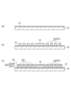
図1~図3を参照して、コイル部品1の構成について説明する。図1は、本発明の一実施形態に係るコイル部品を示す斜視図である。図2は、図1のII-II線に沿った断面図である。図3は、図1のコイル部品1の一部分解斜視図である。なお、図3においては、後述の磁性樹脂層7の図示を省略している。
The configuration of the
図1に示されるコイル部品1は、例えば、直流回路の電圧変換を行うスイッチング電源回路ユニット等に搭載される部品である。図1~図3に示されるように、コイル部品1は、磁性基板10と、コイル部20と、磁性樹脂層7と、導体ポスト19A,19Bと、カバー絶縁層30と、外部端子40A,40Bとを備えている。
A
なお、本明細書中において「積層方向」とは、磁性基板10、コイル部20、磁性樹脂層7、カバー絶縁層30、外部端子40A,40Bというように、磁性基板10から外部端子40A,40Bに向けて各層が順次重なる方向である。また、以下の説明では、積層方向に沿って外部端子40A,40B側を「上」、積層方向に沿って磁性基板10側を「下」として説明する場合がある。
In this specification, the term "laminating direction" refers to the
磁性基板10は、例えばフェライト等の磁性材料によって構成された平板状の基板である。磁性基板10上には、コイル部20が積層されている。コイル部20は磁性樹脂層7に覆われている。磁性樹脂層7は、磁性フィラー及びバインダ樹脂(樹脂)を含む混合物である。磁性樹脂層7は主面7aを有しており、主面7a上には、カバー絶縁層30が積層されている。カバー絶縁層30上には、外部端子40A,40Bが設けられている。
The
コイル部20は、下部絶縁層21と、下部絶縁層21に対して積層された第1平面コイル22と、第1平面コイル22に対して積層された第2平面コイル23と、第1平面コイル22と第2平面コイル23とを電気的に接続するビア導体25と、第1平面コイル22と導体ポスト19Bとを電気的に接続する連結部26と、を備えている。また、コイル部20は、磁性樹脂層7側の主面20aと、主面20aとは反対側(磁性基板10側)の主面20bと、を有している。
The
下部絶縁層21は、磁性基板10上に積層されている。下部絶縁層21は、磁性基板10の全面に設けられている。下部絶縁層21の下側(磁性基板10側)の主面は、コイル部20の主面20bに相当する。
A lower insulating
第1平面コイル22は、磁性基板10に直交し、積層方向に沿った軸線Aを有し、矩形環状を呈している。第1平面コイル22は、軸線Aを中心として矩形状に巻回された第1巻線部(巻線部)221と、第1巻線部221を覆う第1絶縁部222とを含む。ここで、第1絶縁部222が「第1巻線部221を覆う」とは、少なくとも第1巻線部221の一方側(上側、すなわち第2平面コイル23側)の主面221a、及び主面221aに連続する第1巻線部221の側面が第1絶縁部222に接触する状態をいう。第1巻線部221は、下部絶縁層21に対して積層されており、第1巻線部221の下側(磁性基板10側)の主面は、下部絶縁層21に接触している。第1巻線部221は、例えば銅(Cu)等の金属材料によって構成されている。
The first
第1絶縁部222は、2つの絶縁層222A,222Bを含んでいる。絶縁層222Aは、第1巻線部221と同一層内において、第1巻線部221の周囲を埋めている。また、絶縁層222Aは、第1巻線部221の巻回部分同士の間を埋めている。絶縁層222Bは、第1巻線部221の一方側の主面221aに接触している。コイル部20の内径に対応する第1絶縁部222の領域には、積層方向に第1絶縁部222を貫通する貫通孔が形成されている。また、第1絶縁部222には、第1絶縁部222を貫通する貫通孔22aが設けられている。貫通孔22aは、第1絶縁部222の絶縁層222Bに形成されている。なお、本実施形態では、絶縁層222A,222Bは一体に設けられているが、絶縁層222Aと絶縁層222Bとは別の層として設けられていてもよい。また、第1絶縁部222は、下部絶縁層21を含んでいてもよい。
The first insulating
第2平面コイル23は、第1平面コイル22と同様に矩形環状を呈している。第2平面コイル23は、軸線Aを中心として矩形状に巻回された第2巻線部231と、第2巻線部231を覆う第2絶縁部232とを含む。ここで、第2絶縁部232が「第2巻線部231を覆う」とは、少なくとも第2巻線部231の一方側(上側、すなわち磁性樹脂層7側)の主面231a、及び主面231aに連続する第2巻線部231の側面が第2絶縁部232に接触する状態をいう。第2巻線部231は第1絶縁部222に対して積層されており、第2巻線部231の下側(第1絶縁部222側)の主面は、第1絶縁部222(絶縁層222B)に接触している。第2巻線部231は、例えば銅(Cu)等の金属材料によって構成されている。
The second
第2絶縁部232は、2つの絶縁層232A,232Bを含んでいる。絶縁層232Aは、第2巻線部231と同一層内において、第2巻線部231の周囲を埋めている。また、絶縁層232Aは、第2巻線部231の巻回部分同士の間を埋めている。絶縁層232Bは、第2巻線部231の一方側(上側、すなわち磁性樹脂層7側)の主面231aを覆っている。コイル部20の内径に対応する第2絶縁部232の領域には、積層方向に第2絶縁部232を貫通する貫通孔が形成されている。第2絶縁部232の上側の主面は、コイル部20の主面20aに相当する。なお、本実施形態では、絶縁層232A,232Bは一体に設けられているが、絶縁層232Aと絶縁層232Bとは別の層として設けられていてもよい。
The second
下部絶縁層21、第1絶縁部222、及び第2絶縁部232は、絶縁性樹脂によって構成されている。絶縁性樹脂としては、例えばポリイミド、又はポリエチレンテレフタレート等が挙げられる。なお、下部絶縁層21、第1絶縁部222、及び第2絶縁部232は、それぞれ同じ材料によって構成されていてもよいし、異なる材料によって構成されていてもよい。
The lower insulating
ビア導体25は、第1絶縁部222を貫通する貫通孔22a内に設けられている。ビア導体25は、第1巻線部221の最も内側の巻回部分と、第2巻線部231の最も内側の巻回部分とを電気的に接続している。これにより、第1平面コイル22及び第2平面コイル23によって1つのコイルが形成されている。なお、図2に示されるようにビア導体25は、第2巻線部231と一体に設けられていてもよい。連結部26は、第1巻線部221の外側の端部から絶縁層222B及び絶縁層232Aを貫通して磁性樹脂層7の主面7a側に延び、第1巻線部221と導体ポスト19Bとを電気的に接続している。
Via
磁性樹脂層7は、コイル部20の周囲を被覆している。磁性樹脂層7は、直方体形状の外形を有している。直方体形状には、角部及び稜線部が面取りされた直方体の形状、及び、角部及び稜線部が丸められた直方体の形状が含まれる。磁性樹脂層7の主面7aは、長辺及び短辺を有する矩形状をなしている。磁性樹脂層7は、第1磁性樹脂層71と、第2磁性樹脂層72と、を有している。
The
第1磁性樹脂層71は、コイル部20に接触しながら、コイル部20の周囲を覆っている。本実施形態においては、第1磁性樹脂層71はコイル部20の側面及びコイル部20の主面20aを全て覆っており、コイル部20の主面20aに接触している。また、第1磁性樹脂層71は、コイル部20の内径に対応する部分に充填されている。
The first
第1磁性樹脂層71は、磁性フィラー及びバインダ樹脂(樹脂)を含む混合物によって構成されている。第1磁性樹脂層71に含まれる磁性フィラーの構成材料は、例えば鉄、カルボニル鉄、ケイ素、クロム、ニッケル、又はホウ素等である。バインダ樹脂の構成材料は、例えばエポキシ樹脂等である。第1磁性樹脂層71に含まれる磁性フィラーの割合は、例えば第1磁性樹脂層71の全体に対して90重量%以上である。第1磁性樹脂層71に含まれるバインダ樹脂の割合は、例えば第1磁性樹脂層71の全体に対して3重量%以上である。第1磁性樹脂層71に含まれる磁性フィラーの最大粒径は、例えば40μm以上80μm以下である。
The first
第2磁性樹脂層72は、第1磁性樹脂層71に対して積層されている。本実施形態においては、第2磁性樹脂層72はコイル部20の主面20aを覆う第1磁性樹脂層71上に設けられている。したがって、第2磁性樹脂層72とコイル部20とは互いに離間している。第2磁性樹脂層72は、コイル部20とは反対側の主面72aを有している。第2磁性樹脂層72の主面72aは、磁性樹脂層7の主面7aに相当する。
The second
第2磁性樹脂層72は、第1磁性樹脂層71と同様に、磁性フィラー及びバインダ樹脂(樹脂)を含む混合物によって構成されている。第2磁性樹脂層72に含まれる磁性フィラーの構成材料は、例えば鉄、カルボニル鉄、ケイ素、クロム、ニッケル、又はホウ素等である。バインダ樹脂の構成材料は、例えばエポキシ樹脂等である。第2磁性樹脂層72に含まれる磁性フィラーの割合は、例えば第2磁性樹脂層72の全体の90重量%以上である。第2磁性樹脂層72に含まれるバインダ樹脂の割合は、例えば第2磁性樹脂層72の全体に対して3重量%以上である。第2磁性樹脂層72に含まれる磁性フィラーの最大粒径は、第1磁性樹脂層71に含まれる磁性フィラーの最大粒径より小さく、例えば1μm以上10μm以下である。また、第2磁性樹脂層72に含まれる磁性フィラーの最大粒径は、積層方向におけるコイル部20の第2磁性樹脂層72側(磁性樹脂層7側)の主面20aと、第2磁性樹脂層72のコイル部20とは反対側の主面72a(磁性樹脂層7の主面7a)との間の距離Lの10%以下とすることができる。距離Lは、コイル部20の主面20aの上方に設けられた磁性樹脂層7の厚さに相当する。第2磁性樹脂層72の厚さT72は、距離Lより小さくなっている。一例として、距離Lは100μm以上200μm以下程度であり、第2磁性樹脂層72の厚さT72は10μm以上20μm以下程度である。
The second
一対の導体ポスト19A,19Bは、例えば銅(Cu)で構成されており、積層方向に交差する交差方向におけるコイル部20の両端部から積層方向に沿って延びている。導体ポスト19Aは、第2巻線部231の外側の端部に接続されている。導体ポスト19Aは、磁性樹脂層7(第1磁性樹脂層71及び第2磁性樹脂層72)を貫通するように第2巻線部231から磁性樹脂層7の主面7aまで延びて、主面7aに露出している。導体ポスト19Aの露出した部分に対応する位置には、外部端子40Aが設けられている。導体ポスト19Aは、カバー絶縁層30の貫通孔31a内の導体部31によって、外部端子40Aに接続されている。これにより、導体ポスト19A及び導体部31を介して、第2巻線部231の外側の端部(コイル部20の一端部)と外部端子40Aとが電気的に接続されている。
The pair of
導体ポスト19Bは、連結部26に接続されている。導体ポスト19Bは、磁性樹脂層7を貫通するように連結部26から磁性樹脂層7の主面7aまで延びて、主面7aに露出している。導体ポスト19Bの露出した部分に対応する位置には、外部端子40Bが設けられている。導体ポスト19Bは、カバー絶縁層30の貫通孔32a内の導体部32によって、外部端子40Bに接続されている。これにより、連結部26、導体ポスト19B、及び導体部32を介して、第1巻線部221の外側の端部(コイル部20の他端部)と外部端子40Bとが電気的に接続されている。
The
外部端子40Aは、主面7aにおける一方の短辺に沿っており、外部端子40Bは、主面7aにおける他方の短辺に沿っている。外部端子40A,40Bは、主面7aにおける長辺に沿った方向に互いに離間している。一対の外部端子40A,40Bはいずれも膜状であり、平面視で長方形状である。外部端子40A,40Bは、それぞれ、導体ポスト19A,19Bと電気的に接続されている。外部端子40A,40Bは、例えば銅(Cu)等の導電性材料によって構成されている。外部端子40A,40Bは、例えばめっきにより形成され得る。なお、外部端子40A,40Bは、単層構造であってもよいし、複数の層が積層された積層構造であってもよい。
The
カバー絶縁層30は、磁性樹脂層7(第1磁性樹脂層71)の主面7a上に設けられ、積層方向において導体ポスト19A,19Bと外部端子40A,40Bとの間に位置している。カバー絶縁層30は、導体ポスト19A,19Bに対応する位置に貫通孔31a,32aを有している。貫通孔31a,32a内には、銅(Cu)等の導電性材料よって構成された導体部31,32が設けられている。カバー絶縁層30は、絶縁性材料によって構成されており、例えば、ポリイミド、エポキシ等の絶縁性樹脂で構成されている。
The insulating
次に、図4~図7を参照して、コイル部品1の製造方法について説明する。図4~図7は、コイル部品1の製造方法を説明するための図である。
Next, a method for manufacturing the
まず、磁性基板10上にコイル部20を形成する。具体的には、図4(a)に示されるように、磁性基板10の上に絶縁性ペーストパターンを塗布して硬化させることにより下部絶縁層21を形成する。続いて、図4(b)に示されるように、下部絶縁層21の上に金属層14を形成する。金属層14は、例えばめっき又はスパッタリング等により形成することができる。その後、所定のマスクを用いてパターニングを行うことにより、第1巻線部221が形成される。続いて、図4(c)に示されるように、第1絶縁部222を形成する。第1絶縁部222は、金属層14上に絶縁性ペーストパターンを塗布して硬化させることにより形成することができる。このとき、第1絶縁部222の絶縁層222A及び絶縁層222Bが一度に形成される。
First, the
続いて、図5(a)に示されるように、第1絶縁部222(絶縁層222B)をエッチングすることにより、貫通孔22a及び連結部26の一部を形成するための開口16を形成する。これにより、第1平面コイル22が形成された状態となる。
Subsequently, as shown in FIG. 5A, the first insulating portion 222 (insulating
次に、図5(b)に示されるように、めっき又はスパッタリング等により、第2絶縁部232の上に再び金属層14を形成する。その後、所定のマスクを用いてパターニングを行うことにより、第2巻線部231が形成される。このとき、貫通孔22a内にはビア導体25が形成される。また、開口16に対応する位置に連結部26が形成される。
Next, as shown in FIG. 5B, the
次に、図5(c)に示されるように、第2絶縁部232を形成する。第2絶縁部232は、金属層14(第2巻線部231)上に絶縁性ペーストパターンを塗布して硬化させることにより形成することができる。このとき、第2絶縁部232の絶縁層232A及び絶縁層232Bが一度に形成される。これにより、第2平面コイル23が形成された状態となる。
Next, as shown in FIG. 5C, a second insulating
次に、図6(a)に示されるように、第2絶縁部232(絶縁層232B)をエッチングし、導体ポスト19A,19Bを形成するための開口19A’,19B’を形成する。以上の工程により、コイル部20が形成された状態となる。
Next, as shown in FIG. 6A, the second insulating portion 232 (insulating
次に、図6(b)に示されるように、金属層14のうち、第1巻線部221及び第2巻線部231を構成していない部分(第1平面コイル22及び第2平面コイル23の内径部及び外周部に対応する部分)をエッチング処理等によって除去する。
Next, as shown in FIG. 6B, portions of the
次に、図6(c)に示されるように、導体ポスト19A,19Bを形成する。具体的には、所定のマスクを用いてめっきやスパッタリング等により、第2絶縁部232の開口19A’,19B’上にシード部を形成し、このシード部を用いて導体ポスト19A,19Bをめっき形成する。導体ポスト19A,19Bをめっき形成する際には、例えば絶縁性の犠牲層(二点鎖線で示される部分)を用いることができる。
Next, as shown in FIG. 6(c), conductor posts 19A and 19B are formed. Specifically, a seed portion is formed on the
次に、図7(a)に示されるように、磁性基板10の全面に磁性フィラー及び樹脂を含む磁性樹脂を塗布し、硬化処理を行うことにより、第1磁性樹脂層71を形成する。これにより、コイル部20の主面20a及び導体ポスト19A,19Bの周囲の一部が第1磁性樹脂層71によって覆われた状態となる。このとき、コイル部20の内径部分にも第1磁性樹脂層71が充填される。その後、第1磁性樹脂層71に対し、第1磁性樹脂層71に含まれる磁性フィラーよりも最大粒径が小さい磁性フィラーを含む磁性樹脂を塗布し、第2磁性樹脂層72を形成する。これにより、導体ポスト19A,19Bの周囲が第1磁性樹脂層71及び第2磁性樹脂層72によって覆われた状態となる。
Next, as shown in FIG. 7A, a first
次に、第2磁性樹脂層72の表面を研磨することにより、磁性樹脂層7の主面7aを形成する。第2磁性樹脂層72は、例えばグラインディング等の公知の方法によって研磨することができる。一例として、#400程度のホイールを300~6000rpmで回転させることにより、第2磁性樹脂層72の研磨が行われる。このように研磨を行うことにより、平坦な主面7aが得られる。
Next, by polishing the surface of the second
次に、図7(b)に示されるように、磁性樹脂層7の主面7aの上に絶縁性樹脂ペースト等の絶縁性材料を塗布することにより、カバー絶縁層30を形成する。カバー絶縁層30を形成する際、主面7aの全体を覆うと共に、一対の導体ポスト19A、19Bに対応する位置に貫通孔31a、32aを形成し、カバー絶縁層30から一対の導体ポスト19A、19Bを露出させる。具体的には、主面7aの全領域に絶縁性材料を塗布し、その後、導体ポスト19A、19Bに対応する箇所のカバー絶縁層30を除去する。
Next, as shown in FIG. 7B, an insulating
次に、所定のマスクを用いてめっきやスパッタリング等により、カバー絶縁層30上に外部端子40A,40Bに対応する領域にシード部を形成する。シード部は、カバー絶縁層30の貫通孔31a,32aから露出する導体ポスト19A,19B上に形成される。次に、シード部を用いて、無電解めっきにより外部端子40A,40Bを形成する。このとき、カバー絶縁層30の貫通孔31a,32aを埋めるようにめっきが成長して導体部31,32が形成される。以上の工程により、図2に示されるコイル部品1が形成される。
Next, seed portions are formed on the insulating
以上説明したように、コイル部品1の磁性樹脂層7は、コイル部20に接触する第1磁性樹脂層71と、第1磁性樹脂層71に対して積層された第2磁性樹脂層72と、を有している。また、第2磁性樹脂層72に含まれる磁性フィラーの最大粒径は、第1磁性樹脂層71に含まれる磁性フィラーの最大粒径より小さい。このように、相対的に小さい磁性フィラーを含む第2磁性樹脂層72が第1磁性樹脂層71に対して積層され、第2磁性樹脂層72が磁性樹脂層7の主面7aを構成しているので、コイル部品1の製造過程においては第2磁性樹脂層72が研磨される。第2磁性樹脂層に含まれる磁性フィラーの最大粒径は相対的に小さいので、研磨時に第2磁性樹脂層72から磁性フィラーが脱落したとしても、磁性フィラーの脱落による磁性樹脂層の体積の減少量が少ない。したがって、コイル部品1の透磁率の低下が抑制され、その結果インダクタンスの低下を抑制することができる。
As described above, the
図8は、図1のコイル部品1の効果を説明するための図である。図8は、積層方向におけるコイル部20の第2磁性樹脂層72側(磁性樹脂層7側)の主面20aと、第2磁性樹脂層72のコイル部20とは反対側(図示上方)の主面72a(磁性樹脂層7の主面7a)との間の距離Lとインダクタンスとの関係のシミュレーション結果を示している。なお、シミュレーションには三次元電磁界シミュレータ(有限要素法)を使用し、マクスウェルの電磁界方程式を数値シミュレーションにより解いた。図8は1MHzにおけるインダクタンス値を示している。このシミュレーションでは、距離Lの値を160μm、135μm(約15%減少)、110μm(約30%減少)と変化させたときのコイル部品1のインダクタンスの値をそれぞれ調べている。すなわち、このシミュレーションでは、距離Lの値が160μmである場合を基準とし、距離Lの値を135μm、110μmと減少させることにより、磁性フィラーの脱落によって磁性樹脂層7の体積が減少した状態を擬似的に表している。
FIG. 8 is a diagram for explaining the effect of the
図8に示されるように、距離Lを減少させるにつれて、コイル部品1のインダクタンスの値が低下している。すなわち、磁性樹脂層7の体積が減少するほど、コイル部品1のインダクタンスが低下する。このように、図8に示されるシミュレーション結果から、第2磁性樹脂層72に含まれる最大粒径が相対的に小さい磁性フィラーが脱落したとしても、磁性樹脂層7の体積の減少量が少ないので、コイル部品1のインダクタンスの低下が抑制されることが確認できる。
As shown in FIG. 8, as the distance L is decreased, the inductance value of the
また、第2磁性樹脂層72に含まれる磁性フィラーの最大粒径は、積層方向におけるコイル部20の第2磁性樹脂層72側の主面20aと、第2磁性樹脂層72のコイル部20とは反対側の主面7aとの間の距離Lの10%以下である。このように第2磁性樹脂層72に含まれる磁性フィラーの最大粒径を設定することにより、磁束が通過する部分の大きさに対する磁性フィラーの大きさの割合が小さくなる。したがって、磁性フィラーの脱落による透磁率への影響が小さくなり、コイル部品1のインダクタンスの低下が抑制される。
In addition, the maximum particle size of the magnetic filler contained in the second
また、第2磁性樹脂層72の厚さT72は、積層方向におけるコイル部20の第2磁性樹脂層72側の主面20aと、第2磁性樹脂層72のコイル部20とは反対側の主面7aとの間の距離Lより小さい。これにより、磁性樹脂層7において第1磁性樹脂層71が占める割合を大きくすることができる。第1磁性樹脂層71に含まれる磁性フィラーの最大粒径は第2磁性樹脂層72に含まれる磁性フィラーの最大粒径より大きいので、第1磁性樹脂層71の透磁率は第2磁性樹脂層72の透磁率より大きい。したがって、磁性樹脂層7において第1磁性樹脂層71が占める割合を大きくすることで磁性樹脂層7全体での透磁率を大きくすることができる。よって、コイル部品1としての透磁率を大きくすることができる。
In addition, the thickness T72 of the second
また、本実施形態に係るコイル部品1の製造方法では、第2磁性樹脂層72を研磨することにより、磁性樹脂層7の主面7aが形成される。第2磁性樹脂層72に含まれる磁性フィラーの最大粒径は相対的に小さいので、研磨により第2磁性樹脂層72から磁性フィラーが脱落したとしても、磁性フィラーの脱落による磁性樹脂層7の体積の減少量が少ない。したがって、コイル部品1の透磁率の低下が抑制され、その結果インダクタンスの低下を抑制することができる。
Further, in the method of manufacturing the
また、第2磁性樹脂層72を研磨して磁性樹脂層7の主面7aを形成することにより、コイル部品1の表面の平坦性の向上を図ることができる。これにより、コイル部品1を基板等に実装する際に、コイル部品1の取り付けを容易に行うことができる。一例として、コイル部品1と、コイル部品1が実装される基板との間にアンダーフィル材を充填する場合、コイル部品1の表面が平坦であることによりアンダーフィル材の充填を容易に行うことができる。
Further, by polishing the second
次に、図9を参照して、変形例に係るコイル部品2について説明する。図9は、変形例に係るコイル部品を概略的に示す断面図である。図9に示されるように、コイル部品2は、コイル部品1と同様に、磁性基板10と、コイル部20と、第1磁性樹脂層71と、第2磁性樹脂層72と、導体ポスト19A,19Bと、カバー絶縁層30と、外部端子40A,40Bとを備えている。コイル部品2がコイル部品1と相違する点は、第2磁性樹脂層72の厚さが、積層方向におけるコイル部20の第2磁性樹脂層72側の主面20aと、第2磁性樹脂層72のコイル部20とは反対側の主面7aとの間の距離L以上である点である。第2磁性樹脂層72はコイル部20の主面20aに接触している。第1磁性樹脂層71は、コイル部20の主面20aよりも下側(磁性基板10側)においてコイル部20の周囲及びコイル部20の内径に対応する部分に充填されている。
Next, a
上記のコイル部品2においても、コイル部品1と同様に、相対的に小さい磁性フィラーを含む第2磁性樹脂層72が第1磁性樹脂層71に対して積層されているので、コイル部品2の製造過程においては第2磁性樹脂層72が研磨される。第2磁性樹脂層に含まれる磁性フィラーの最大粒径は相対的に小さいので、第2磁性樹脂層72から磁性フィラーが脱落したとしても、磁性フィラーの脱落による磁性樹脂層の体積の減少量が少ない。したがって、コイル部品2の透磁率の低下が抑制され、その結果インダクタンスの低下を抑制することができる。
In the
また、第2磁性樹脂層72の厚さT72は、積層方向におけるコイル部20の第2磁性樹脂層72側の主面20aと、第2磁性樹脂層72のコイル部20とは反対側の主面20aとの間の距離L以上である。これにより、第2磁性樹脂層72はコイル部20に接触する。第2磁性樹脂層72に含まれる磁性フィラーの最大粒径は第1磁性樹脂層71に含まれる磁性フィラーの最大粒径より小さいので、第2磁性樹脂層72とコイル部20との密着性は、第1磁性樹脂層71とコイル部20との密着性より高い。したがって、第2磁性樹脂層72とコイル部20とが接触することにより、磁性樹脂層7とコイル部20との密着性を高めることができる。
In addition, the thickness T72 of the second
次に、図10を参照して、変形例に係るコイル部品3について説明する。図10は、変形例に係るコイル部品を概略的に示す断面図である。図10に示されるように、コイル部品3は、コイル部品1と同様に、コイル部20と、第1磁性樹脂層71と、第2磁性樹脂層72と、導体ポスト19A,19Bと、カバー絶縁層30と、外部端子40A,40Bとを備えている。コイル部品3がコイル部品1と相違する点は、磁性樹脂層7が、第1磁性樹脂層71に対して第2磁性樹脂層72とは反対側(コイル部20の主面20aとは反対側)に積層された第3磁性樹脂層73を更に有する点である。すなわち、コイル部品3は、磁性基板10に代えて、磁性樹脂層7に含まれる第3磁性樹脂層73を備えている。第3磁性樹脂層はコイル部20の主面20bに接触している。
Next, a
第3磁性樹脂層73は、第2磁性樹脂層72と同様に、磁性フィラー及びバインダ樹脂(樹脂)を含む混合物によって構成されている。第3磁性樹脂層73に含まれる磁性フィラーの構成材料は、例えば鉄、カルボニル鉄、ケイ素、クロム、ニッケル、又はホウ素等である。バインダ樹脂の構成材料は、例えばエポキシ樹脂等である。第3磁性樹脂層73に含まれる磁性フィラーの割合は、例えば第3磁性樹脂層73の全体の90重量%以上である。第3磁性樹脂層73に含まれるバインダ樹脂の割合は、例えば第3磁性樹脂層73の全体の3重量%以上である。第3磁性樹脂層73に含まれる磁性フィラーの最大粒径は、第1磁性樹脂層71に含まれる磁性フィラーの最大粒径より小さく、例えば1μm以上10μm以下である。
Like the second
次に、コイル部品3の製造方法について説明する。コイル部品3の製造方法では、コイル部品1の製造方法と同様の工程を行った後、磁性基板10を研磨又は機械的な剥離等によって除去する。その後、磁性基板10の除去によって露出した面(コイル部20の主面20b)に磁性樹脂を塗布して第3磁性樹脂層73を形成することにより、図10に示されるコイル部品3が形成される。なお、コイル部品3の製造方法では、図4(a)に示される最初の工程から磁性基板10を用いずに、研磨又は剥離が容易な基材を用いてもよい。
Next, a method for manufacturing the
上記のコイル部品3においても、コイル部品1と同様に、相対的に小さい磁性フィラーを含む第2磁性樹脂層72が第1磁性樹脂層71に対して積層されているので、コイル部品1と同様の効果を得ることができる。また、コイル部品3では、コイル部20の主面20a側に第2磁性樹脂層72が設けられ、コイル部20の主面20aとは反対側(主面20b側)に、相対的に小さい磁性フィラーを含む第3磁性樹脂層73が形成されるので、積層方向におけるコイル部品3の対称性が向上する。したがって、応力等によるコイル部品3の反りを抑制することができる。なお、対称性の観点から、第3磁性樹脂層73に含まれる磁性フィラーの最大粒径は、第2磁性樹脂層72に含まれる磁性フィラーの最大粒径と同様であることが好ましい。
In the
次に、図11を参照して、コイル部品3の変形例に係るコイル部品4について説明する。図11は、変形例に係るコイル部品を概略的に示す断面図である。図11に示されるように、コイル部品4は、コイル部品3と同様に、第1磁性樹脂層71と、第2磁性樹脂層72と、第3磁性樹脂層73と、外部端子40A,40Bとを備えている。コイル部品4がコイル部品3と相違する点は、コイル部20に代えてコイル部50を備える点、及び外部端子40A,40Bがコイル部品4の一方の主面ではなく側面に設けられている点である。
Next, a
コイル部50では、第1巻線部221の最も外側の一端及び第2巻線部231の最も外側の一端は、それぞれコイル部50の側面から露出している。第1巻線部221及び第2巻線部231が露出するコイル部50の側面は、第1磁性樹脂層71の側面から露出している。すなわち、第1巻線部221の最も外側の一端及び第2巻線部231の最も外側の一端は、コイル部品4の側面において露出している。外部端子40Aは第2巻線部231が露出した部分においてコイル部品4の側面に設けられており、第2巻線部231と直接電気的に接続されている。外部端子40Bは、第1巻線部221が露出した部分においてコイル部品4の側面に設けられており、第1巻線部221と直接電気的に接続されている。
In the
上記のコイル部品4は、コイル部品3と同様に、コイル部50の主面50a側に第2磁性樹脂層72が設けられ、コイル部50の主面50aとは反対側(主面20b側)に、相対的に小さい磁性フィラーを含む第3磁性樹脂層73が設けられている。したがって、コイル部品4においてもコイル部品3と同様の効果を得ることができる。また、コイル部品4では、第1磁性樹脂層71及び第2磁性樹脂層72内に導体ポストが設けられていないので、導体ポストによって第1磁性樹脂層71及び第2磁性樹脂層72の体積が減少することを抑制することができる。
Like the
以上、本発明の実施形態について説明してきたが、本発明は上記の実施形態に限定されず、種々の変更を行うことができる。例えば、上記の実施形態においては、コイル部20が2つの巻線部(第1巻線部221及び第2巻線部231)を有する例について説明したが、コイル部20は、1つの巻線部を有していてもよいし、3つ以上の巻線部を有していてもよい。
Although the embodiments of the present invention have been described above, the present invention is not limited to the above embodiments, and various modifications can be made. For example, in the above-described embodiment, the
1,2,3,4…コイル部品、7…磁性樹脂層、7a,20a,50a…主面、20,50…コイル部、22…第1平面コイル(平面コイル)、71…第1磁性樹脂層、72…第2磁性樹脂層、73…第3磁性樹脂層、221…第1巻線部(巻線部)、222…第1絶縁部(絶縁部)、L…距離。
DESCRIPTION OF
Claims (4)
前記コイル部の上方を被覆し、磁性フィラーを含む磁性樹脂層と、を備え、
前記磁性樹脂層は、前記コイル部の側面を全て覆い、
前記磁性樹脂層は、前記コイル部に接触する第1磁性樹脂層と、前記第1磁性樹脂層上に積層された第2磁性樹脂層と、を有し、
前記第2磁性樹脂層は前記磁性樹脂層の主面を構成し、
前記第2磁性樹脂層に含まれる磁性フィラーの最大粒径は、前記第1磁性樹脂層に含まれる磁性フィラーの最大粒径より小さく、
前記平面コイルは、前記磁性樹脂層の上方の主面上に配置された一対の外部端子に対して下方に設けられ、
前記一対の外部端子と前記平面コイルとは、前記磁性樹脂層を貫通するように形成された導体ポストを介して接続され、
前記第2磁性樹脂層の厚さは、積層方向における前記コイル部の前記第2磁性樹脂層側の主面と、前記第2磁性樹脂層の前記コイル部とは反対側の主面との間の距離以上である、コイル部品。 a coil portion having a planar coil including a winding portion and an insulating portion covering the winding portion;
A magnetic resin layer covering the upper part of the coil part and containing a magnetic filler,
The magnetic resin layer covers all side surfaces of the coil portion,
The magnetic resin layer has a first magnetic resin layer in contact with the coil portion and a second magnetic resin layer laminated on the first magnetic resin layer,
The second magnetic resin layer constitutes the main surface of the magnetic resin layer,
The maximum particle size of the magnetic filler contained in the second magnetic resin layer is smaller than the maximum particle size of the magnetic filler contained in the first magnetic resin layer,
The planar coil is provided below a pair of external terminals arranged on the main surface above the magnetic resin layer,
The pair of external terminals and the planar coil are connected via a conductor post formed to penetrate the magnetic resin layer ,
The thickness of the second magnetic resin layer is between the main surface of the coil portion on the side of the second magnetic resin layer and the main surface of the second magnetic resin layer opposite to the coil portion in the stacking direction. coil components that are greater than or equal to the distance of
前記第3磁性樹脂層に含まれる磁性フィラーの最大粒径は、前記第1磁性樹脂層に含まれる磁性フィラーの最大粒径より小さい、請求項1または2に記載のコイル部品。 The magnetic resin layer has a third magnetic resin layer laminated on the side opposite to the second magnetic resin layer with respect to the first magnetic resin layer,
3. The coil component according to claim 1, wherein the maximum particle size of the magnetic filler contained in said third magnetic resin layer is smaller than the maximum particle size of the magnetic filler contained in said first magnetic resin layer.
前記コイル部の周囲において前記コイル部に接触し、磁性フィラーを含む第1磁性樹脂層を形成する工程と、
前記第1磁性樹脂層上に、前記第1磁性樹脂層に含まれる前記磁性フィラーよりも最大粒径が小さい磁性フィラーを含む第2磁性樹脂層を積層することで、前記第1磁性樹脂層及び前記第2磁性樹脂層により、前記コイル部の側面を全て覆った状態で前記コイル部を被覆する磁性樹脂層を形成する工程と、
前記第2磁性樹脂層を研磨し、前記磁性樹脂層の主面を形成する工程と、を含み、
前記磁性樹脂層を形成する工程では、前記磁性樹脂層の主面上に配置される一対の外部端子と、前記一対の外部端子に対して下方に設けられる前記平面コイルとを接続する導体ポストの周囲を前記第1磁性樹脂層及び前記第2磁性樹脂層が覆うように前記磁性樹脂層を形成し、
前記第2磁性樹脂層の厚さは、積層方向における前記コイル部の前記第2磁性樹脂層側の主面と、前記第2磁性樹脂層の前記コイル部とは反対側の主面との間の距離以上である、コイル部品の製造方法。 forming a coil portion having a planar coil including a winding portion and an insulating portion covering the winding portion;
forming a first magnetic resin layer containing a magnetic filler in contact with the coil portion around the coil portion;
By laminating a second magnetic resin layer containing a magnetic filler having a smaller maximum particle size than the magnetic filler contained in the first magnetic resin layer on the first magnetic resin layer, the first magnetic resin layer and forming a magnetic resin layer covering the coil portion with the second magnetic resin layer covering all side surfaces of the coil portion;
polishing the second magnetic resin layer to form a main surface of the magnetic resin layer;
In the step of forming the magnetic resin layer, conductor posts connecting a pair of external terminals arranged on the main surface of the magnetic resin layer and the planar coil provided below the pair of external terminals are formed. forming the magnetic resin layer so that the first magnetic resin layer and the second magnetic resin layer cover the periphery;
The thickness of the second magnetic resin layer is between the main surface of the coil portion on the side of the second magnetic resin layer and the main surface of the second magnetic resin layer opposite to the coil portion in the stacking direction. A method for manufacturing a coil component , wherein the distance is greater than or equal to
Priority Applications (2)
| Application Number | Priority Date | Filing Date | Title |
|---|---|---|---|
| JP2017178179A JP7307524B2 (en) | 2017-09-15 | 2017-09-15 | COIL COMPONENT AND COIL COMPONENT MANUFACTURING METHOD |
| US16/126,351 US11488772B2 (en) | 2017-09-15 | 2018-09-10 | Coil component and method of manufacturing the same |
Applications Claiming Priority (1)
| Application Number | Priority Date | Filing Date | Title |
|---|---|---|---|
| JP2017178179A JP7307524B2 (en) | 2017-09-15 | 2017-09-15 | COIL COMPONENT AND COIL COMPONENT MANUFACTURING METHOD |
Publications (2)
| Publication Number | Publication Date |
|---|---|
| JP2019054144A JP2019054144A (en) | 2019-04-04 |
| JP7307524B2 true JP7307524B2 (en) | 2023-07-12 |
Family
ID=65720513
Family Applications (1)
| Application Number | Title | Priority Date | Filing Date |
|---|---|---|---|
| JP2017178179A Active JP7307524B2 (en) | 2017-09-15 | 2017-09-15 | COIL COMPONENT AND COIL COMPONENT MANUFACTURING METHOD |
Country Status (2)
| Country | Link |
|---|---|
| US (1) | US11488772B2 (en) |
| JP (1) | JP7307524B2 (en) |
Families Citing this family (4)
| Publication number | Priority date | Publication date | Assignee | Title |
|---|---|---|---|---|
| US10720788B2 (en) * | 2015-10-09 | 2020-07-21 | Taiwan Semiconductor Manufacturing Company, Ltd. | Wireless charging devices having wireless charging coils and methods of manufacture thereof |
| CN111066106B (en) * | 2017-08-28 | 2023-04-04 | Tdk株式会社 | Coil component and method for manufacturing same |
| US11854731B2 (en) | 2018-08-31 | 2023-12-26 | Taiyo Yuden Co., Ltd. | Coil component and electronic device |
| JP7169128B2 (en) * | 2018-08-31 | 2022-11-10 | 太陽誘電株式会社 | Coil parts and electronic equipment |
Citations (2)
| Publication number | Priority date | Publication date | Assignee | Title |
|---|---|---|---|---|
| JP2013135208A (en) | 2011-12-22 | 2013-07-08 | Samsung Electro-Mechanics Co Ltd | Filter for removing noise and method of manufacturing the same |
| JP2017103354A (en) | 2015-12-02 | 2017-06-08 | Tdk株式会社 | Coil component and power supply circuit unit |
Family Cites Families (20)
| Publication number | Priority date | Publication date | Assignee | Title |
|---|---|---|---|---|
| US6998939B2 (en) * | 2000-03-08 | 2006-02-14 | Matsushita Electric Industrial Co., Ltd. | Noise filter and electronic device using noise filter |
| US7119649B2 (en) * | 2004-05-28 | 2006-10-10 | Matsushita Electric Industrial Co., Ltd. | Common mode noise filter |
| JP4736526B2 (en) * | 2005-05-11 | 2011-07-27 | パナソニック株式会社 | Common mode noise filter |
| JP5115691B2 (en) * | 2006-12-28 | 2013-01-09 | Tdk株式会社 | Coil device and method of manufacturing coil device |
| US8505192B2 (en) * | 2010-10-08 | 2013-08-13 | Advance Furnace Systems Corp. | Manufacturing method of common mode filter |
| US8601673B2 (en) * | 2010-11-25 | 2013-12-10 | Cyntec Co., Ltd. | Method of producing an inductor with a high inductance |
| CN103764592B (en) * | 2011-09-02 | 2016-04-20 | 株式会社村田制作所 | The manufacture method of ferrite ceramics composition, ceramic electronic components and ceramic electronic components |
| KR101862401B1 (en) * | 2011-11-07 | 2018-05-30 | 삼성전기주식회사 | Layered Inductor and Manufacturing Method fo the Same |
| KR101883003B1 (en) * | 2011-12-14 | 2018-08-27 | 삼성전기주식회사 | Filter for Removing Noise And Method of The Same |
| KR101541581B1 (en) * | 2012-06-28 | 2015-08-03 | 삼성전기주식회사 | Inductor and manufacturing method of the inductor |
| KR20140001673A (en) * | 2012-06-28 | 2014-01-07 | 삼성전기주식회사 | Common mode noise filter |
| KR20140071770A (en) * | 2012-12-04 | 2014-06-12 | 삼성전기주식회사 | Common mode noise chip filter and method for preparing thereof |
| KR101983136B1 (en) * | 2012-12-28 | 2019-09-10 | 삼성전기주식회사 | Power inductor and manufacturing method thereof |
| KR20140116678A (en) * | 2013-03-25 | 2014-10-06 | 삼성전기주식회사 | Thin film common mode filter and method of manufacturing the same |
| CN105122394A (en) * | 2013-04-18 | 2015-12-02 | 松下知识产权经营株式会社 | Common mode noise filter and manufacturing method thereof |
| KR101580399B1 (en) * | 2014-06-24 | 2015-12-23 | 삼성전기주식회사 | Chip electronic component and manufacturing method thereof |
| KR101662207B1 (en) * | 2014-09-11 | 2016-10-06 | 주식회사 모다이노칩 | Power inductor |
| KR101607026B1 (en) * | 2014-11-04 | 2016-03-28 | 삼성전기주식회사 | Chip electronic component and manufacturing method thereof |
| JP6477427B2 (en) | 2015-11-04 | 2019-03-06 | 株式会社村田製作所 | Coil parts |
| JP6672756B2 (en) * | 2015-12-04 | 2020-03-25 | 株式会社村田製作所 | Electronic component and method of manufacturing electronic component |
-
2017
- 2017-09-15 JP JP2017178179A patent/JP7307524B2/en active Active
-
2018
- 2018-09-10 US US16/126,351 patent/US11488772B2/en active Active
Patent Citations (2)
| Publication number | Priority date | Publication date | Assignee | Title |
|---|---|---|---|---|
| JP2013135208A (en) | 2011-12-22 | 2013-07-08 | Samsung Electro-Mechanics Co Ltd | Filter for removing noise and method of manufacturing the same |
| JP2017103354A (en) | 2015-12-02 | 2017-06-08 | Tdk株式会社 | Coil component and power supply circuit unit |
Also Published As
| Publication number | Publication date |
|---|---|
| US20190088413A1 (en) | 2019-03-21 |
| US11488772B2 (en) | 2022-11-01 |
| JP2019054144A (en) | 2019-04-04 |
Similar Documents
| Publication | Publication Date | Title |
|---|---|---|
| JP7307524B2 (en) | COIL COMPONENT AND COIL COMPONENT MANUFACTURING METHOD | |
| JP5614479B2 (en) | Coil parts manufacturing method | |
| JP7172113B2 (en) | Coil component and its manufacturing method | |
| US11854730B2 (en) | Coil component and method of manufacturing coil component | |
| KR101762039B1 (en) | Coil component | |
| JP6984212B2 (en) | Coil parts | |
| JP5113025B2 (en) | Coil structure and manufacturing method thereof | |
| JP6429609B2 (en) | Coil component and manufacturing method thereof | |
| CN112908611B (en) | Coil component | |
| JP6716867B2 (en) | Coil component and manufacturing method thereof | |
| US20190295763A1 (en) | Inductor and method of manufacturing the same | |
| JP2020038940A (en) | Inductor and method of manufacturing the same | |
| JP5375878B2 (en) | Coil component manufacturing method and coil component | |
| JP6443451B2 (en) | High frequency components | |
| JP6878983B2 (en) | Coil parts and manufacturing method of coil parts | |
| JP2018170320A (en) | Coil component and manufacturing method of the same | |
| JP6893761B2 (en) | Coil parts manufacturing method, coil parts, and power supply circuit unit | |
| WO2021079697A1 (en) | Coil component and method for manufacturing same | |
| JP6819395B2 (en) | Coil parts | |
| JP2017103360A (en) | Coil component and power supply circuit unit | |
| JP2017199718A (en) | Electronic component and method for manufacturing the same | |
| WO2016059918A1 (en) | Electronic component | |
| JP6984220B2 (en) | Coil parts | |
| JP7073650B2 (en) | Coil parts | |
| JP6428204B2 (en) | Coil component and manufacturing method thereof |
Legal Events
| Date | Code | Title | Description |
|---|---|---|---|
| A621 | Written request for application examination |
Free format text: JAPANESE INTERMEDIATE CODE: A621 Effective date: 20200622 |
|
| A977 | Report on retrieval |
Free format text: JAPANESE INTERMEDIATE CODE: A971007 Effective date: 20210531 |
|
| A131 | Notification of reasons for refusal |
Free format text: JAPANESE INTERMEDIATE CODE: A131 Effective date: 20210706 |
|
| A521 | Request for written amendment filed |
Free format text: JAPANESE INTERMEDIATE CODE: A523 Effective date: 20210903 |
|
| A02 | Decision of refusal |
Free format text: JAPANESE INTERMEDIATE CODE: A02 Effective date: 20220208 |
|
| A521 | Request for written amendment filed |
Free format text: JAPANESE INTERMEDIATE CODE: A523 Effective date: 20220502 |
|
| C60 | Trial request (containing other claim documents, opposition documents) |
Free format text: JAPANESE INTERMEDIATE CODE: C60 Effective date: 20220502 |
|
| C11 | Written invitation by the commissioner to file amendments |
Free format text: JAPANESE INTERMEDIATE CODE: C11 Effective date: 20220517 |
|
| A911 | Transfer to examiner for re-examination before appeal (zenchi) |
Free format text: JAPANESE INTERMEDIATE CODE: A911 Effective date: 20220617 |
|
| C21 | Notice of transfer of a case for reconsideration by examiners before appeal proceedings |
Free format text: JAPANESE INTERMEDIATE CODE: C21 Effective date: 20220621 |
|
| A912 | Re-examination (zenchi) completed and case transferred to appeal board |
Free format text: JAPANESE INTERMEDIATE CODE: A912 Effective date: 20220902 |
|
| C211 | Notice of termination of reconsideration by examiners before appeal proceedings |
Free format text: JAPANESE INTERMEDIATE CODE: C211 Effective date: 20220906 |
|
| C22 | Notice of designation (change) of administrative judge |
Free format text: JAPANESE INTERMEDIATE CODE: C22 Effective date: 20230124 |
|
| C13 | Notice of reasons for refusal |
Free format text: JAPANESE INTERMEDIATE CODE: C13 Effective date: 20230307 |
|
| C22 | Notice of designation (change) of administrative judge |
Free format text: JAPANESE INTERMEDIATE CODE: C22 Effective date: 20230411 |
|
| A521 | Request for written amendment filed |
Free format text: JAPANESE INTERMEDIATE CODE: A523 Effective date: 20230428 |
|
| A61 | First payment of annual fees (during grant procedure) |
Free format text: JAPANESE INTERMEDIATE CODE: A61 Effective date: 20230630 |
|
| R150 | Certificate of patent or registration of utility model |
Ref document number: 7307524 Country of ref document: JP Free format text: JAPANESE INTERMEDIATE CODE: R150 |