JP7306695B2 - Implants that use ultrasound to stimulate tissue - Google Patents
Implants that use ultrasound to stimulate tissue Download PDFInfo
- Publication number
- JP7306695B2 JP7306695B2 JP2019500515A JP2019500515A JP7306695B2 JP 7306695 B2 JP7306695 B2 JP 7306695B2 JP 2019500515 A JP2019500515 A JP 2019500515A JP 2019500515 A JP2019500515 A JP 2019500515A JP 7306695 B2 JP7306695 B2 JP 7306695B2
- Authority
- JP
- Japan
- Prior art keywords
- ultrasound
- implantable device
- transducer
- implantable
- tissue
- Prior art date
- Legal status (The legal status is an assumption and is not a legal conclusion. Google has not performed a legal analysis and makes no representation as to the accuracy of the status listed.)
- Active
Links
- 238000002604 ultrasonography Methods 0.000 title claims description 342
- 239000007943 implant Substances 0.000 title claims description 33
- 210000001519 tissue Anatomy 0.000 claims description 183
- 230000004044 response Effects 0.000 claims description 65
- 238000004146 energy storage Methods 0.000 claims description 49
- 210000003205 muscle Anatomy 0.000 claims description 39
- 230000033001 locomotion Effects 0.000 claims description 31
- 239000000560 biocompatible material Substances 0.000 claims description 23
- 210000000944 nerve tissue Anatomy 0.000 claims description 19
- 210000000056 organ Anatomy 0.000 claims description 17
- 210000002027 skeletal muscle Anatomy 0.000 claims description 17
- 210000001428 peripheral nervous system Anatomy 0.000 claims description 13
- 241000282414 Homo sapiens Species 0.000 claims description 12
- 210000003169 central nervous system Anatomy 0.000 claims description 11
- 150000002500 ions Chemical class 0.000 claims description 11
- 210000004165 myocardium Anatomy 0.000 claims description 11
- 210000002460 smooth muscle Anatomy 0.000 claims description 11
- 230000008520 organization Effects 0.000 claims description 7
- 229910052451 lead zirconate titanate Inorganic materials 0.000 description 105
- 239000000758 substrate Substances 0.000 description 76
- 239000004593 Epoxy Substances 0.000 description 68
- 239000000463 material Substances 0.000 description 68
- 238000000034 method Methods 0.000 description 66
- 230000001537 neural effect Effects 0.000 description 60
- 239000013078 crystal Substances 0.000 description 49
- 238000004891 communication Methods 0.000 description 45
- 230000000638 stimulation Effects 0.000 description 42
- BQCADISMDOOEFD-UHFFFAOYSA-N Silver Chemical compound [Ag] BQCADISMDOOEFD-UHFFFAOYSA-N 0.000 description 41
- 238000005259 measurement Methods 0.000 description 40
- 210000005036 nerve Anatomy 0.000 description 40
- 239000000428 dust Substances 0.000 description 39
- 229910052709 silver Inorganic materials 0.000 description 38
- 239000004332 silver Substances 0.000 description 38
- 238000012360 testing method Methods 0.000 description 36
- XLYOFNOQVPJJNP-UHFFFAOYSA-N water Substances O XLYOFNOQVPJJNP-UHFFFAOYSA-N 0.000 description 33
- 229910000679 solder Inorganic materials 0.000 description 32
- HBMJWWWQQXIZIP-UHFFFAOYSA-N silicon carbide Chemical compound [Si+]#[C-] HBMJWWWQQXIZIP-UHFFFAOYSA-N 0.000 description 31
- 238000010586 diagram Methods 0.000 description 25
- 230000005540 biological transmission Effects 0.000 description 23
- 239000004205 dimethyl polysiloxane Substances 0.000 description 21
- 229920000435 poly(dimethylsiloxane) Polymers 0.000 description 21
- 230000006870 function Effects 0.000 description 20
- 238000001727 in vivo Methods 0.000 description 20
- 229910010271 silicon carbide Inorganic materials 0.000 description 20
- 229920001721 polyimide Polymers 0.000 description 18
- 210000003497 sciatic nerve Anatomy 0.000 description 18
- 239000004642 Polyimide Substances 0.000 description 17
- 241000700159 Rattus Species 0.000 description 17
- 238000003491 array Methods 0.000 description 17
- 239000002131 composite material Substances 0.000 description 17
- 230000008569 process Effects 0.000 description 17
- SOGAXMICEFXMKE-UHFFFAOYSA-N Butylmethacrylate Chemical compound CCCCOC(=O)C(C)=C SOGAXMICEFXMKE-UHFFFAOYSA-N 0.000 description 16
- 238000002474 experimental method Methods 0.000 description 16
- 238000004088 simulation Methods 0.000 description 16
- 239000000919 ceramic Substances 0.000 description 15
- 230000008859 change Effects 0.000 description 15
- 229920000052 poly(p-xylylene) Polymers 0.000 description 15
- BASFCYQUMIYNBI-UHFFFAOYSA-N platinum Substances [Pt] BASFCYQUMIYNBI-UHFFFAOYSA-N 0.000 description 14
- 239000000523 sample Substances 0.000 description 14
- 230000004936 stimulating effect Effects 0.000 description 14
- 238000005516 engineering process Methods 0.000 description 13
- PCHJSUWPFVWCPO-UHFFFAOYSA-N gold Chemical compound [Au] PCHJSUWPFVWCPO-UHFFFAOYSA-N 0.000 description 13
- 230000002829 reductive effect Effects 0.000 description 13
- VYPSYNLAJGMNEJ-UHFFFAOYSA-N silicon dioxide Inorganic materials O=[Si]=O VYPSYNLAJGMNEJ-UHFFFAOYSA-N 0.000 description 13
- PXHVJJICTQNCMI-UHFFFAOYSA-N Nickel Chemical compound [Ni] PXHVJJICTQNCMI-UHFFFAOYSA-N 0.000 description 12
- 239000003990 capacitor Substances 0.000 description 12
- 238000004519 manufacturing process Methods 0.000 description 12
- 238000013461 design Methods 0.000 description 11
- 238000005538 encapsulation Methods 0.000 description 11
- 229910052737 gold Inorganic materials 0.000 description 11
- 239000010931 gold Substances 0.000 description 11
- 239000012071 phase Substances 0.000 description 11
- 238000000623 plasma-assisted chemical vapour deposition Methods 0.000 description 11
- 238000012545 processing Methods 0.000 description 11
- 238000005476 soldering Methods 0.000 description 11
- 241001465754 Metazoa Species 0.000 description 10
- 239000000853 adhesive Substances 0.000 description 10
- 230000001070 adhesive effect Effects 0.000 description 10
- 238000013459 approach Methods 0.000 description 10
- 230000008878 coupling Effects 0.000 description 10
- 238000010168 coupling process Methods 0.000 description 10
- 238000005859 coupling reaction Methods 0.000 description 10
- 238000003860 storage Methods 0.000 description 10
- 235000012239 silicon dioxide Nutrition 0.000 description 9
- 239000000243 solution Substances 0.000 description 9
- GWEVSGVZZGPLCZ-UHFFFAOYSA-N Titan oxide Chemical compound O=[Ti]=O GWEVSGVZZGPLCZ-UHFFFAOYSA-N 0.000 description 8
- XLOMVQKBTHCTTD-UHFFFAOYSA-N Zinc monoxide Chemical compound [Zn]=O XLOMVQKBTHCTTD-UHFFFAOYSA-N 0.000 description 8
- 210000004556 brain Anatomy 0.000 description 8
- 238000004422 calculation algorithm Methods 0.000 description 8
- 238000012512 characterization method Methods 0.000 description 8
- 230000001054 cortical effect Effects 0.000 description 8
- 230000000694 effects Effects 0.000 description 8
- 230000001965 increasing effect Effects 0.000 description 8
- 238000009738 saturating Methods 0.000 description 8
- VRBFTYUMFJWSJY-UHFFFAOYSA-N 28804-46-8 Chemical compound ClC1CC(C=C2)=CC=C2C(Cl)CC2=CC=C1C=C2 VRBFTYUMFJWSJY-UHFFFAOYSA-N 0.000 description 7
- PNEYBMLMFCGWSK-UHFFFAOYSA-N aluminium oxide Inorganic materials [O-2].[O-2].[O-2].[Al+3].[Al+3] PNEYBMLMFCGWSK-UHFFFAOYSA-N 0.000 description 7
- 229910021417 amorphous silicon Inorganic materials 0.000 description 7
- 230000001684 chronic effect Effects 0.000 description 7
- 230000006378 damage Effects 0.000 description 7
- 238000002513 implantation Methods 0.000 description 7
- 230000007774 longterm Effects 0.000 description 7
- 229910052751 metal Inorganic materials 0.000 description 7
- 239000002184 metal Substances 0.000 description 7
- 230000003071 parasitic effect Effects 0.000 description 7
- 210000000578 peripheral nerve Anatomy 0.000 description 7
- -1 poly(3,4-ethylenedioxythiophene) Polymers 0.000 description 7
- 238000012546 transfer Methods 0.000 description 7
- WHNWPMSKXPGLAX-UHFFFAOYSA-N N-Vinyl-2-pyrrolidone Chemical compound C=CN1CCCC1=O WHNWPMSKXPGLAX-UHFFFAOYSA-N 0.000 description 6
- 241000283984 Rodentia Species 0.000 description 6
- 230000036982 action potential Effects 0.000 description 6
- WYTGDNHDOZPMIW-RCBQFDQVSA-N alstonine Natural products C1=CC2=C3C=CC=CC3=NC2=C2N1C[C@H]1[C@H](C)OC=C(C(=O)OC)[C@H]1C2 WYTGDNHDOZPMIW-RCBQFDQVSA-N 0.000 description 6
- 230000006399 behavior Effects 0.000 description 6
- 238000006243 chemical reaction Methods 0.000 description 6
- 239000008393 encapsulating agent Substances 0.000 description 6
- 238000001914 filtration Methods 0.000 description 6
- 239000011521 glass Substances 0.000 description 6
- 229910052759 nickel Inorganic materials 0.000 description 6
- 229920000642 polymer Polymers 0.000 description 6
- 230000009467 reduction Effects 0.000 description 6
- 238000013519 translation Methods 0.000 description 6
- 241000283690 Bos taurus Species 0.000 description 5
- 241000282472 Canis lupus familiaris Species 0.000 description 5
- 241000282693 Cercopithecidae Species 0.000 description 5
- 241000282326 Felis catus Species 0.000 description 5
- 241000287828 Gallus gallus Species 0.000 description 5
- 241001494479 Pecora Species 0.000 description 5
- 229920001609 Poly(3,4-ethylenedioxythiophene) Polymers 0.000 description 5
- 229910000831 Steel Inorganic materials 0.000 description 5
- 229910002113 barium titanate Inorganic materials 0.000 description 5
- 235000013330 chicken meat Nutrition 0.000 description 5
- 239000011248 coating agent Substances 0.000 description 5
- 238000000576 coating method Methods 0.000 description 5
- 150000001875 compounds Chemical class 0.000 description 5
- 238000012790 confirmation Methods 0.000 description 5
- 238000000151 deposition Methods 0.000 description 5
- 238000001514 detection method Methods 0.000 description 5
- 230000005669 field effect Effects 0.000 description 5
- HFGPZNIAWCZYJU-UHFFFAOYSA-N lead zirconate titanate Chemical compound [O-2].[O-2].[O-2].[O-2].[O-2].[Ti+4].[Zr+4].[Pb+2] HFGPZNIAWCZYJU-UHFFFAOYSA-N 0.000 description 5
- 239000000203 mixture Substances 0.000 description 5
- 239000004033 plastic Substances 0.000 description 5
- 229920003023 plastic Polymers 0.000 description 5
- 229910052697 platinum Inorganic materials 0.000 description 5
- 239000010453 quartz Substances 0.000 description 5
- 230000001105 regulatory effect Effects 0.000 description 5
- 238000011160 research Methods 0.000 description 5
- 229910052710 silicon Inorganic materials 0.000 description 5
- 230000003595 spectral effect Effects 0.000 description 5
- 239000010959 steel Substances 0.000 description 5
- 239000010409 thin film Substances 0.000 description 5
- 230000007704 transition Effects 0.000 description 5
- 241000283707 Capra Species 0.000 description 4
- 239000002033 PVDF binder Substances 0.000 description 4
- 229910052581 Si3N4 Inorganic materials 0.000 description 4
- XUIMIQQOPSSXEZ-UHFFFAOYSA-N Silicon Chemical compound [Si] XUIMIQQOPSSXEZ-UHFFFAOYSA-N 0.000 description 4
- RTAQQCXQSZGOHL-UHFFFAOYSA-N Titanium Chemical compound [Ti] RTAQQCXQSZGOHL-UHFFFAOYSA-N 0.000 description 4
- 238000004458 analytical method Methods 0.000 description 4
- 229920000249 biocompatible polymer Polymers 0.000 description 4
- 239000002775 capsule Substances 0.000 description 4
- 210000003710 cerebral cortex Anatomy 0.000 description 4
- 238000007906 compression Methods 0.000 description 4
- 230000006835 compression Effects 0.000 description 4
- 229920001577 copolymer Polymers 0.000 description 4
- 238000005520 cutting process Methods 0.000 description 4
- 238000011161 development Methods 0.000 description 4
- 230000018109 developmental process Effects 0.000 description 4
- 239000010408 film Substances 0.000 description 4
- 230000004907 flux Effects 0.000 description 4
- 229910000154 gallium phosphate Inorganic materials 0.000 description 4
- 238000010438 heat treatment Methods 0.000 description 4
- 238000002847 impedance measurement Methods 0.000 description 4
- 238000001566 impedance spectroscopy Methods 0.000 description 4
- 238000009413 insulation Methods 0.000 description 4
- 210000002414 leg Anatomy 0.000 description 4
- 230000003278 mimic effect Effects 0.000 description 4
- 210000002569 neuron Anatomy 0.000 description 4
- 229910052758 niobium Inorganic materials 0.000 description 4
- 239000010955 niobium Substances 0.000 description 4
- GUCVJGMIXFAOAE-UHFFFAOYSA-N niobium atom Chemical compound [Nb] GUCVJGMIXFAOAE-UHFFFAOYSA-N 0.000 description 4
- 230000035515 penetration Effects 0.000 description 4
- 229920003223 poly(pyromellitimide-1,4-diphenyl ether) Polymers 0.000 description 4
- 229920000647 polyepoxide Polymers 0.000 description 4
- 229920002981 polyvinylidene fluoride Polymers 0.000 description 4
- 239000004065 semiconductor Substances 0.000 description 4
- 239000010703 silicon Substances 0.000 description 4
- 239000000377 silicon dioxide Substances 0.000 description 4
- HQVNEWCFYHHQES-UHFFFAOYSA-N silicon nitride Chemical compound N12[Si]34N5[Si]62N3[Si]51N64 HQVNEWCFYHHQES-UHFFFAOYSA-N 0.000 description 4
- 210000000278 spinal cord Anatomy 0.000 description 4
- 229910001220 stainless steel Inorganic materials 0.000 description 4
- 239000010935 stainless steel Substances 0.000 description 4
- 239000010936 titanium Substances 0.000 description 4
- 229910052719 titanium Inorganic materials 0.000 description 4
- 239000011787 zinc oxide Substances 0.000 description 4
- GKWLILHTTGWKLQ-UHFFFAOYSA-N 2,3-dihydrothieno[3,4-b][1,4]dioxine Chemical compound O1CCOC2=CSC=C21 GKWLILHTTGWKLQ-UHFFFAOYSA-N 0.000 description 3
- 241000283086 Equidae Species 0.000 description 3
- 206010061218 Inflammation Diseases 0.000 description 3
- 241000124008 Mammalia Species 0.000 description 3
- 241000699670 Mus sp. Species 0.000 description 3
- 229910021607 Silver chloride Inorganic materials 0.000 description 3
- FAPWRFPIFSIZLT-UHFFFAOYSA-M Sodium chloride Chemical compound [Na+].[Cl-] FAPWRFPIFSIZLT-UHFFFAOYSA-M 0.000 description 3
- 241000282887 Suidae Species 0.000 description 3
- NIXOWILDQLNWCW-UHFFFAOYSA-N acrylic acid group Chemical group C(C=C)(=O)O NIXOWILDQLNWCW-UHFFFAOYSA-N 0.000 description 3
- 230000003213 activating effect Effects 0.000 description 3
- 229910052782 aluminium Inorganic materials 0.000 description 3
- XAGFODPZIPBFFR-UHFFFAOYSA-N aluminium Chemical compound [Al] XAGFODPZIPBFFR-UHFFFAOYSA-N 0.000 description 3
- 230000004888 barrier function Effects 0.000 description 3
- 210000004227 basal ganglia Anatomy 0.000 description 3
- 230000008901 benefit Effects 0.000 description 3
- 210000005013 brain tissue Anatomy 0.000 description 3
- 210000004027 cell Anatomy 0.000 description 3
- 210000001638 cerebellum Anatomy 0.000 description 3
- 229920001940 conductive polymer Polymers 0.000 description 3
- 229910021419 crystalline silicon Inorganic materials 0.000 description 3
- 230000008021 deposition Effects 0.000 description 3
- 201000010099 disease Diseases 0.000 description 3
- 208000037265 diseases, disorders, signs and symptoms Diseases 0.000 description 3
- 238000006073 displacement reaction Methods 0.000 description 3
- 125000003700 epoxy group Chemical group 0.000 description 3
- 210000001320 hippocampus Anatomy 0.000 description 3
- 229910052588 hydroxylapatite Inorganic materials 0.000 description 3
- 210000003016 hypothalamus Anatomy 0.000 description 3
- 230000004054 inflammatory process Effects 0.000 description 3
- 230000010354 integration Effects 0.000 description 3
- 238000003698 laser cutting Methods 0.000 description 3
- 230000000670 limiting effect Effects 0.000 description 3
- 239000007788 liquid Substances 0.000 description 3
- 238000013289 male long evans rat Methods 0.000 description 3
- 210000001767 medulla oblongata Anatomy 0.000 description 3
- 210000001259 mesencephalon Anatomy 0.000 description 3
- VNWKTOKETHGBQD-UHFFFAOYSA-N methane Chemical compound C VNWKTOKETHGBQD-UHFFFAOYSA-N 0.000 description 3
- 230000000116 mitigating effect Effects 0.000 description 3
- 238000012544 monitoring process Methods 0.000 description 3
- 239000000178 monomer Substances 0.000 description 3
- 210000001087 myotubule Anatomy 0.000 description 3
- 230000004007 neuromodulation Effects 0.000 description 3
- XYJRXVWERLGGKC-UHFFFAOYSA-D pentacalcium;hydroxide;triphosphate Chemical compound [OH-].[Ca+2].[Ca+2].[Ca+2].[Ca+2].[Ca+2].[O-]P([O-])([O-])=O.[O-]P([O-])([O-])=O.[O-]P([O-])([O-])=O XYJRXVWERLGGKC-UHFFFAOYSA-D 0.000 description 3
- 230000010363 phase shift Effects 0.000 description 3
- 210000002975 pon Anatomy 0.000 description 3
- 239000002243 precursor Substances 0.000 description 3
- 206010039073 rheumatoid arthritis Diseases 0.000 description 3
- 230000035945 sensitivity Effects 0.000 description 3
- 238000009958 sewing Methods 0.000 description 3
- 201000002859 sleep apnea Diseases 0.000 description 3
- 239000007787 solid Substances 0.000 description 3
- 238000001356 surgical procedure Methods 0.000 description 3
- 230000002123 temporal effect Effects 0.000 description 3
- 210000001103 thalamus Anatomy 0.000 description 3
- 230000001225 therapeutic effect Effects 0.000 description 3
- 238000010200 validation analysis Methods 0.000 description 3
- 210000003905 vulva Anatomy 0.000 description 3
- WKBPZYKAUNRMKP-UHFFFAOYSA-N 1-[2-(2,4-dichlorophenyl)pentyl]1,2,4-triazole Chemical compound C=1C=C(Cl)C=C(Cl)C=1C(CCC)CN1C=NC=N1 WKBPZYKAUNRMKP-UHFFFAOYSA-N 0.000 description 2
- WSMQKESQZFQMFW-UHFFFAOYSA-N 5-methyl-pyrazole-3-carboxylic acid Chemical compound CC1=CC(C(O)=O)=NN1 WSMQKESQZFQMFW-UHFFFAOYSA-N 0.000 description 2
- PIGFYZPCRLYGLF-UHFFFAOYSA-N Aluminum nitride Chemical compound [Al]#N PIGFYZPCRLYGLF-UHFFFAOYSA-N 0.000 description 2
- 206010002091 Anaesthesia Diseases 0.000 description 2
- 229920000049 Carbon (fiber) Polymers 0.000 description 2
- RYGMFSIKBFXOCR-UHFFFAOYSA-N Copper Chemical compound [Cu] RYGMFSIKBFXOCR-UHFFFAOYSA-N 0.000 description 2
- 241001050985 Disco Species 0.000 description 2
- 241000283073 Equus caballus Species 0.000 description 2
- 241000282412 Homo Species 0.000 description 2
- 229910003334 KNbO3 Inorganic materials 0.000 description 2
- YQEZLKZALYSWHR-UHFFFAOYSA-N Ketamine Chemical compound C=1C=CC=C(Cl)C=1C1(NC)CCCCC1=O YQEZLKZALYSWHR-UHFFFAOYSA-N 0.000 description 2
- 229910003327 LiNbO3 Inorganic materials 0.000 description 2
- 229910012463 LiTaO3 Inorganic materials 0.000 description 2
- FYYHWMGAXLPEAU-UHFFFAOYSA-N Magnesium Chemical compound [Mg] FYYHWMGAXLPEAU-UHFFFAOYSA-N 0.000 description 2
- 241000699666 Mus <mouse, genus> Species 0.000 description 2
- 229910020347 Na2WO3 Inorganic materials 0.000 description 2
- 241000283973 Oryctolagus cuniculus Species 0.000 description 2
- 241000282898 Sus scrofa Species 0.000 description 2
- 241000251539 Vertebrata <Metazoa> Species 0.000 description 2
- 238000010521 absorption reaction Methods 0.000 description 2
- 239000008186 active pharmaceutical agent Substances 0.000 description 2
- 230000001154 acute effect Effects 0.000 description 2
- 210000000577 adipose tissue Anatomy 0.000 description 2
- 229910000147 aluminium phosphate Inorganic materials 0.000 description 2
- 230000037005 anaesthesia Effects 0.000 description 2
- JRPBQTZRNDNNOP-UHFFFAOYSA-N barium titanate Chemical compound [Ba+2].[Ba+2].[O-][Ti]([O-])([O-])[O-] JRPBQTZRNDNNOP-UHFFFAOYSA-N 0.000 description 2
- 230000002051 biphasic effect Effects 0.000 description 2
- 229910052797 bismuth Inorganic materials 0.000 description 2
- JCXGWMGPZLAOME-UHFFFAOYSA-N bismuth atom Chemical compound [Bi] JCXGWMGPZLAOME-UHFFFAOYSA-N 0.000 description 2
- 230000000903 blocking effect Effects 0.000 description 2
- 238000004364 calculation method Methods 0.000 description 2
- 238000011088 calibration curve Methods 0.000 description 2
- 229910052799 carbon Inorganic materials 0.000 description 2
- 239000004917 carbon fiber Substances 0.000 description 2
- 238000000354 decomposition reaction Methods 0.000 description 2
- 238000000708 deep reactive-ion etching Methods 0.000 description 2
- 230000001934 delay Effects 0.000 description 2
- 230000006866 deterioration Effects 0.000 description 2
- 206010012601 diabetes mellitus Diseases 0.000 description 2
- 239000012153 distilled water Substances 0.000 description 2
- 238000002592 echocardiography Methods 0.000 description 2
- 238000009713 electroplating Methods 0.000 description 2
- 238000005265 energy consumption Methods 0.000 description 2
- 238000005530 etching Methods 0.000 description 2
- 230000000763 evoking effect Effects 0.000 description 2
- 238000000605 extraction Methods 0.000 description 2
- 210000003195 fascia Anatomy 0.000 description 2
- 238000010304 firing Methods 0.000 description 2
- 230000036541 health Effects 0.000 description 2
- 238000009434 installation Methods 0.000 description 2
- 229960003299 ketamine Drugs 0.000 description 2
- 210000003734 kidney Anatomy 0.000 description 2
- 210000002429 large intestine Anatomy 0.000 description 2
- 230000002045 lasting effect Effects 0.000 description 2
- 238000012886 linear function Methods 0.000 description 2
- GQYHUHYESMUTHG-UHFFFAOYSA-N lithium niobate Chemical compound [Li+].[O-][Nb](=O)=O GQYHUHYESMUTHG-UHFFFAOYSA-N 0.000 description 2
- 238000011670 long-evans rat Methods 0.000 description 2
- 229910052749 magnesium Inorganic materials 0.000 description 2
- 239000011777 magnesium Substances 0.000 description 2
- 239000000155 melt Substances 0.000 description 2
- 229910044991 metal oxide Inorganic materials 0.000 description 2
- 150000004706 metal oxides Chemical class 0.000 description 2
- 239000011140 metalized polyester Substances 0.000 description 2
- 210000000653 nervous system Anatomy 0.000 description 2
- 239000000615 nonconductor Substances 0.000 description 2
- 238000001208 nuclear magnetic resonance pulse sequence Methods 0.000 description 2
- 238000000059 patterning Methods 0.000 description 2
- 230000004962 physiological condition Effects 0.000 description 2
- 229920006267 polyester film Polymers 0.000 description 2
- UKDIAJWKFXFVFG-UHFFFAOYSA-N potassium;oxido(dioxo)niobium Chemical compound [K+].[O-][Nb](=O)=O UKDIAJWKFXFVFG-UHFFFAOYSA-N 0.000 description 2
- HNJBEVLQSNELDL-UHFFFAOYSA-N pyrrolidin-2-one Chemical compound O=C1CCCN1 HNJBEVLQSNELDL-UHFFFAOYSA-N 0.000 description 2
- 230000005855 radiation Effects 0.000 description 2
- 238000011552 rat model Methods 0.000 description 2
- 229920006395 saturated elastomer Polymers 0.000 description 2
- 230000011664 signaling Effects 0.000 description 2
- 210000003625 skull Anatomy 0.000 description 2
- 210000000813 small intestine Anatomy 0.000 description 2
- XMVONEAAOPAGAO-UHFFFAOYSA-N sodium tungstate Chemical compound [Na+].[Na+].[O-][W]([O-])(=O)=O XMVONEAAOPAGAO-UHFFFAOYSA-N 0.000 description 2
- 238000004544 sputter deposition Methods 0.000 description 2
- 210000002784 stomach Anatomy 0.000 description 2
- 229920002994 synthetic fiber Polymers 0.000 description 2
- 239000011031 topaz Substances 0.000 description 2
- 229910052853 topaz Inorganic materials 0.000 description 2
- WFKWXMTUELFFGS-UHFFFAOYSA-N tungsten Chemical compound [W] WFKWXMTUELFFGS-UHFFFAOYSA-N 0.000 description 2
- BPICBUSOMSTKRF-UHFFFAOYSA-N xylazine Chemical compound CC1=CC=CC(C)=C1NC1=NCCCS1 BPICBUSOMSTKRF-UHFFFAOYSA-N 0.000 description 2
- 229960001600 xylazine Drugs 0.000 description 2
- 229910000859 α-Fe Inorganic materials 0.000 description 2
- 241000271566 Aves Species 0.000 description 1
- OKTJSMMVPCPJKN-UHFFFAOYSA-N Carbon Chemical compound [C] OKTJSMMVPCPJKN-UHFFFAOYSA-N 0.000 description 1
- 241000700198 Cavia Species 0.000 description 1
- 241000288673 Chiroptera Species 0.000 description 1
- 102000004127 Cytokines Human genes 0.000 description 1
- 108090000695 Cytokines Proteins 0.000 description 1
- 101100458289 Drosophila melanogaster msps gene Proteins 0.000 description 1
- 241001269524 Dura Species 0.000 description 1
- WQZGKKKJIJFFOK-GASJEMHNSA-N Glucose Natural products OC[C@H]1OC(O)[C@H](O)[C@@H](O)[C@@H]1O WQZGKKKJIJFFOK-GASJEMHNSA-N 0.000 description 1
- 101100478277 Homo sapiens SPTA1 gene Proteins 0.000 description 1
- WHXSMMKQMYFTQS-UHFFFAOYSA-N Lithium Chemical compound [Li] WHXSMMKQMYFTQS-UHFFFAOYSA-N 0.000 description 1
- 238000007476 Maximum Likelihood Methods 0.000 description 1
- 240000008790 Musa x paradisiaca Species 0.000 description 1
- 235000018290 Musa x paradisiaca Nutrition 0.000 description 1
- 208000012902 Nervous system disease Diseases 0.000 description 1
- 208000025966 Neurological disease Diseases 0.000 description 1
- 239000004677 Nylon Substances 0.000 description 1
- 206010033892 Paraplegia Diseases 0.000 description 1
- 240000007643 Phytolacca americana Species 0.000 description 1
- BLRPTPMANUNPDV-UHFFFAOYSA-N Silane Chemical compound [SiH4] BLRPTPMANUNPDV-UHFFFAOYSA-N 0.000 description 1
- 102100037608 Spectrin alpha chain, erythrocytic 1 Human genes 0.000 description 1
- ATJFFYVFTNAWJD-UHFFFAOYSA-N Tin Chemical compound [Sn] ATJFFYVFTNAWJD-UHFFFAOYSA-N 0.000 description 1
- 230000002745 absorbent Effects 0.000 description 1
- 239000002250 absorbent Substances 0.000 description 1
- 230000004308 accommodation Effects 0.000 description 1
- 230000003044 adaptive effect Effects 0.000 description 1
- 230000002411 adverse Effects 0.000 description 1
- 239000012491 analyte Substances 0.000 description 1
- 229910052586 apatite Inorganic materials 0.000 description 1
- 239000007864 aqueous solution Substances 0.000 description 1
- QVGXLLKOCUKJST-UHFFFAOYSA-N atomic oxygen Chemical compound [O] QVGXLLKOCUKJST-UHFFFAOYSA-N 0.000 description 1
- 230000002238 attenuated effect Effects 0.000 description 1
- 210000003403 autonomic nervous system Anatomy 0.000 description 1
- WQZGKKKJIJFFOK-VFUOTHLCSA-N beta-D-glucose Chemical compound OC[C@H]1O[C@@H](O)[C@H](O)[C@@H](O)[C@@H]1O WQZGKKKJIJFFOK-VFUOTHLCSA-N 0.000 description 1
- 230000033228 biological regulation Effects 0.000 description 1
- 238000001574 biopsy Methods 0.000 description 1
- 230000017531 blood circulation Effects 0.000 description 1
- 210000000988 bone and bone Anatomy 0.000 description 1
- 210000000845 cartilage Anatomy 0.000 description 1
- 231100000190 chronic cytotoxicity Toxicity 0.000 description 1
- 239000004020 conductor Substances 0.000 description 1
- 210000002808 connective tissue Anatomy 0.000 description 1
- 230000001276 controlling effect Effects 0.000 description 1
- 238000001816 cooling Methods 0.000 description 1
- 229910052802 copper Inorganic materials 0.000 description 1
- 239000010949 copper Substances 0.000 description 1
- 239000011889 copper foil Substances 0.000 description 1
- 230000007797 corrosion Effects 0.000 description 1
- 238000005260 corrosion Methods 0.000 description 1
- 238000013144 data compression Methods 0.000 description 1
- 230000003247 decreasing effect Effects 0.000 description 1
- 230000007547 defect Effects 0.000 description 1
- 230000007123 defense Effects 0.000 description 1
- 238000000280 densification Methods 0.000 description 1
- 230000002999 depolarising effect Effects 0.000 description 1
- 238000009795 derivation Methods 0.000 description 1
- 229940079593 drug Drugs 0.000 description 1
- 239000003814 drug Substances 0.000 description 1
- 230000009977 dual effect Effects 0.000 description 1
- 230000001700 effect on tissue Effects 0.000 description 1
- 230000005684 electric field Effects 0.000 description 1
- 239000007772 electrode material Substances 0.000 description 1
- 230000007831 electrophysiology Effects 0.000 description 1
- 238000002001 electrophysiology Methods 0.000 description 1
- 230000001037 epileptic effect Effects 0.000 description 1
- 150000002118 epoxides Chemical class 0.000 description 1
- 239000000284 extract Substances 0.000 description 1
- 210000003414 extremity Anatomy 0.000 description 1
- 210000003746 feather Anatomy 0.000 description 1
- 210000003754 fetus Anatomy 0.000 description 1
- 210000000232 gallbladder Anatomy 0.000 description 1
- 230000002496 gastric effect Effects 0.000 description 1
- 210000004907 gland Anatomy 0.000 description 1
- 239000008103 glucose Substances 0.000 description 1
- 238000000227 grinding Methods 0.000 description 1
- 238000003306 harvesting Methods 0.000 description 1
- 239000005556 hormone Substances 0.000 description 1
- 229940088597 hormone Drugs 0.000 description 1
- BHEPBYXIRTUNPN-UHFFFAOYSA-N hydridophosphorus(.) (triplet) Chemical compound [PH] BHEPBYXIRTUNPN-UHFFFAOYSA-N 0.000 description 1
- 125000002887 hydroxy group Chemical group [H]O* 0.000 description 1
- 238000003384 imaging method Methods 0.000 description 1
- 208000015181 infectious disease Diseases 0.000 description 1
- 230000002757 inflammatory effect Effects 0.000 description 1
- 238000003780 insertion Methods 0.000 description 1
- 230000037431 insertion Effects 0.000 description 1
- 238000007689 inspection Methods 0.000 description 1
- 230000002452 interceptive effect Effects 0.000 description 1
- 229910052741 iridium Inorganic materials 0.000 description 1
- GKOZUEZYRPOHIO-UHFFFAOYSA-N iridium atom Chemical compound [Ir] GKOZUEZYRPOHIO-UHFFFAOYSA-N 0.000 description 1
- 230000007794 irritation Effects 0.000 description 1
- 238000002955 isolation Methods 0.000 description 1
- 210000003127 knee Anatomy 0.000 description 1
- 229910052744 lithium Inorganic materials 0.000 description 1
- 210000004185 liver Anatomy 0.000 description 1
- 238000011068 loading method Methods 0.000 description 1
- 230000005923 long-lasting effect Effects 0.000 description 1
- 210000003141 lower extremity Anatomy 0.000 description 1
- 210000004698 lymphocyte Anatomy 0.000 description 1
- 238000010801 machine learning Methods 0.000 description 1
- 210000002540 macrophage Anatomy 0.000 description 1
- 210000005075 mammary gland Anatomy 0.000 description 1
- 239000011159 matrix material Substances 0.000 description 1
- 238000002844 melting Methods 0.000 description 1
- 230000008018 melting Effects 0.000 description 1
- 238000012986 modification Methods 0.000 description 1
- 230000004048 modification Effects 0.000 description 1
- 210000001616 monocyte Anatomy 0.000 description 1
- 230000003183 myoelectrical effect Effects 0.000 description 1
- 230000008035 nerve activity Effects 0.000 description 1
- 230000007383 nerve stimulation Effects 0.000 description 1
- 230000036403 neuro physiology Effects 0.000 description 1
- 230000003227 neuromodulating effect Effects 0.000 description 1
- 239000002858 neurotransmitter agent Substances 0.000 description 1
- 229910052756 noble gas Inorganic materials 0.000 description 1
- 229920001778 nylon Polymers 0.000 description 1
- 238000005457 optimization Methods 0.000 description 1
- 230000010355 oscillation Effects 0.000 description 1
- 210000001672 ovary Anatomy 0.000 description 1
- 229910052760 oxygen Inorganic materials 0.000 description 1
- 239000001301 oxygen Substances 0.000 description 1
- 239000005022 packaging material Substances 0.000 description 1
- 210000000496 pancreas Anatomy 0.000 description 1
- 239000002245 particle Substances 0.000 description 1
- 230000000149 penetrating effect Effects 0.000 description 1
- VSIIXMUUUJUKCM-UHFFFAOYSA-D pentacalcium;fluoride;triphosphate Chemical compound [F-].[Ca+2].[Ca+2].[Ca+2].[Ca+2].[Ca+2].[O-]P([O-])([O-])=O.[O-]P([O-])([O-])=O.[O-]P([O-])([O-])=O VSIIXMUUUJUKCM-UHFFFAOYSA-D 0.000 description 1
- 230000002093 peripheral effect Effects 0.000 description 1
- 239000008055 phosphate buffer solution Substances 0.000 description 1
- 238000001020 plasma etching Methods 0.000 description 1
- 238000007747 plating Methods 0.000 description 1
- 229920000139 polyethylene terephthalate Polymers 0.000 description 1
- 239000005020 polyethylene terephthalate Substances 0.000 description 1
- 229920005644 polyethylene terephthalate glycol copolymer Polymers 0.000 description 1
- 229920002635 polyurethane Polymers 0.000 description 1
- 239000004814 polyurethane Substances 0.000 description 1
- 230000003334 potential effect Effects 0.000 description 1
- 239000012255 powdered metal Substances 0.000 description 1
- 238000003825 pressing Methods 0.000 description 1
- 230000004224 protection Effects 0.000 description 1
- 230000009979 protective mechanism Effects 0.000 description 1
- 108090000623 proteins and genes Proteins 0.000 description 1
- 102000004169 proteins and genes Human genes 0.000 description 1
- 238000011084 recovery Methods 0.000 description 1
- 230000011514 reflex Effects 0.000 description 1
- 230000029058 respiratory gaseous exchange Effects 0.000 description 1
- 230000000284 resting effect Effects 0.000 description 1
- 210000003079 salivary gland Anatomy 0.000 description 1
- 150000003839 salts Chemical class 0.000 description 1
- 235000015067 sauces Nutrition 0.000 description 1
- 238000010963 scalable process Methods 0.000 description 1
- 230000003248 secreting effect Effects 0.000 description 1
- HKZLPVFGJNLROG-UHFFFAOYSA-M silver monochloride Chemical compound [Cl-].[Ag+] HKZLPVFGJNLROG-UHFFFAOYSA-M 0.000 description 1
- 239000011780 sodium chloride Substances 0.000 description 1
- 230000000392 somatic effect Effects 0.000 description 1
- 210000002466 splanchnic nerve Anatomy 0.000 description 1
- 210000000952 spleen Anatomy 0.000 description 1
- 238000007920 subcutaneous administration Methods 0.000 description 1
- 239000000126 substance Substances 0.000 description 1
- 230000001629 suppression Effects 0.000 description 1
- 238000010301 surface-oxidation reaction Methods 0.000 description 1
- 230000001360 synchronised effect Effects 0.000 description 1
- 230000009885 systemic effect Effects 0.000 description 1
- 238000002560 therapeutic procedure Methods 0.000 description 1
- 238000005979 thermal decomposition reaction Methods 0.000 description 1
- 210000002972 tibial nerve Anatomy 0.000 description 1
- 230000036962 time dependent Effects 0.000 description 1
- 238000013334 tissue model Methods 0.000 description 1
- 230000009466 transformation Effects 0.000 description 1
- 238000000844 transformation Methods 0.000 description 1
- 238000013024 troubleshooting Methods 0.000 description 1
- 229910052721 tungsten Inorganic materials 0.000 description 1
- 239000010937 tungsten Substances 0.000 description 1
- 210000003932 urinary bladder Anatomy 0.000 description 1
- 210000004291 uterus Anatomy 0.000 description 1
- 230000001515 vagal effect Effects 0.000 description 1
- 210000001186 vagus nerve Anatomy 0.000 description 1
- 238000007740 vapor deposition Methods 0.000 description 1
- 239000012808 vapor phase Substances 0.000 description 1
- 230000008016 vaporization Effects 0.000 description 1
- 238000012795 verification Methods 0.000 description 1
- 230000003313 weakening effect Effects 0.000 description 1
- 238000005303 weighing Methods 0.000 description 1
- 210000004885 white matter Anatomy 0.000 description 1
Images


Classifications
-
- A—HUMAN NECESSITIES
- A61—MEDICAL OR VETERINARY SCIENCE; HYGIENE
- A61B—DIAGNOSIS; SURGERY; IDENTIFICATION
- A61B5/00—Measuring for diagnostic purposes; Identification of persons
- A61B5/0002—Remote monitoring of patients using telemetry, e.g. transmission of vital signals via a communication network
- A61B5/0031—Implanted circuitry
-
- A—HUMAN NECESSITIES
- A61—MEDICAL OR VETERINARY SCIENCE; HYGIENE
- A61B—DIAGNOSIS; SURGERY; IDENTIFICATION
- A61B5/00—Measuring for diagnostic purposes; Identification of persons
- A61B5/07—Endoradiosondes
- A61B5/076—Permanent implantations
-
- A—HUMAN NECESSITIES
- A61—MEDICAL OR VETERINARY SCIENCE; HYGIENE
- A61B—DIAGNOSIS; SURGERY; IDENTIFICATION
- A61B5/00—Measuring for diagnostic purposes; Identification of persons
- A61B5/24—Detecting, measuring or recording bioelectric or biomagnetic signals of the body or parts thereof
- A61B5/25—Bioelectric electrodes therefor
- A61B5/279—Bioelectric electrodes therefor specially adapted for particular uses
-
- A—HUMAN NECESSITIES
- A61—MEDICAL OR VETERINARY SCIENCE; HYGIENE
- A61B—DIAGNOSIS; SURGERY; IDENTIFICATION
- A61B5/00—Measuring for diagnostic purposes; Identification of persons
- A61B5/68—Arrangements of detecting, measuring or recording means, e.g. sensors, in relation to patient
- A61B5/6846—Arrangements of detecting, measuring or recording means, e.g. sensors, in relation to patient specially adapted to be brought in contact with an internal body part, i.e. invasive
- A61B5/6847—Arrangements of detecting, measuring or recording means, e.g. sensors, in relation to patient specially adapted to be brought in contact with an internal body part, i.e. invasive mounted on an invasive device
- A61B5/686—Permanently implanted devices, e.g. pacemakers, other stimulators, biochips
-
- A—HUMAN NECESSITIES
- A61—MEDICAL OR VETERINARY SCIENCE; HYGIENE
- A61B—DIAGNOSIS; SURGERY; IDENTIFICATION
- A61B6/00—Apparatus for radiation diagnosis, e.g. combined with radiation therapy equipment
- A61B6/42—Apparatus for radiation diagnosis, e.g. combined with radiation therapy equipment with arrangements for detecting radiation specially adapted for radiation diagnosis
- A61B6/4208—Apparatus for radiation diagnosis, e.g. combined with radiation therapy equipment with arrangements for detecting radiation specially adapted for radiation diagnosis characterised by using a particular type of detector
- A61B6/4258—Apparatus for radiation diagnosis, e.g. combined with radiation therapy equipment with arrangements for detecting radiation specially adapted for radiation diagnosis characterised by using a particular type of detector for detecting non x-ray radiation, e.g. gamma radiation
-
- A—HUMAN NECESSITIES
- A61—MEDICAL OR VETERINARY SCIENCE; HYGIENE
- A61B—DIAGNOSIS; SURGERY; IDENTIFICATION
- A61B8/00—Diagnosis using ultrasonic, sonic or infrasonic waves
- A61B8/08—Detecting organic movements or changes, e.g. tumours, cysts, swellings
- A61B8/0808—Detecting organic movements or changes, e.g. tumours, cysts, swellings for diagnosis of the brain
-
- A—HUMAN NECESSITIES
- A61—MEDICAL OR VETERINARY SCIENCE; HYGIENE
- A61B—DIAGNOSIS; SURGERY; IDENTIFICATION
- A61B8/00—Diagnosis using ultrasonic, sonic or infrasonic waves
- A61B8/08—Detecting organic movements or changes, e.g. tumours, cysts, swellings
- A61B8/0833—Detecting organic movements or changes, e.g. tumours, cysts, swellings involving detecting or locating foreign bodies or organic structures
- A61B8/085—Detecting organic movements or changes, e.g. tumours, cysts, swellings involving detecting or locating foreign bodies or organic structures for locating body or organic structures, e.g. tumours, calculi, blood vessels, nodules
-
- A—HUMAN NECESSITIES
- A61—MEDICAL OR VETERINARY SCIENCE; HYGIENE
- A61B—DIAGNOSIS; SURGERY; IDENTIFICATION
- A61B8/00—Diagnosis using ultrasonic, sonic or infrasonic waves
- A61B8/08—Detecting organic movements or changes, e.g. tumours, cysts, swellings
- A61B8/0875—Detecting organic movements or changes, e.g. tumours, cysts, swellings for diagnosis of bone
-
- A—HUMAN NECESSITIES
- A61—MEDICAL OR VETERINARY SCIENCE; HYGIENE
- A61B—DIAGNOSIS; SURGERY; IDENTIFICATION
- A61B8/00—Diagnosis using ultrasonic, sonic or infrasonic waves
- A61B8/48—Diagnostic techniques
-
- A—HUMAN NECESSITIES
- A61—MEDICAL OR VETERINARY SCIENCE; HYGIENE
- A61N—ELECTROTHERAPY; MAGNETOTHERAPY; RADIATION THERAPY; ULTRASOUND THERAPY
- A61N1/00—Electrotherapy; Circuits therefor
- A61N1/18—Applying electric currents by contact electrodes
- A61N1/32—Applying electric currents by contact electrodes alternating or intermittent currents
- A61N1/36—Applying electric currents by contact electrodes alternating or intermittent currents for stimulation
- A61N1/3605—Implantable neurostimulators for stimulating central or peripheral nerve system
-
- A—HUMAN NECESSITIES
- A61—MEDICAL OR VETERINARY SCIENCE; HYGIENE
- A61N—ELECTROTHERAPY; MAGNETOTHERAPY; RADIATION THERAPY; ULTRASOUND THERAPY
- A61N1/00—Electrotherapy; Circuits therefor
- A61N1/18—Applying electric currents by contact electrodes
- A61N1/32—Applying electric currents by contact electrodes alternating or intermittent currents
- A61N1/36—Applying electric currents by contact electrodes alternating or intermittent currents for stimulation
- A61N1/372—Arrangements in connection with the implantation of stimulators
- A61N1/37205—Microstimulators, e.g. implantable through a cannula
-
- A—HUMAN NECESSITIES
- A61—MEDICAL OR VETERINARY SCIENCE; HYGIENE
- A61N—ELECTROTHERAPY; MAGNETOTHERAPY; RADIATION THERAPY; ULTRASOUND THERAPY
- A61N1/00—Electrotherapy; Circuits therefor
- A61N1/18—Applying electric currents by contact electrodes
- A61N1/32—Applying electric currents by contact electrodes alternating or intermittent currents
- A61N1/36—Applying electric currents by contact electrodes alternating or intermittent currents for stimulation
- A61N1/372—Arrangements in connection with the implantation of stimulators
- A61N1/378—Electrical supply
- A61N1/3787—Electrical supply from an external energy source
-
- B—PERFORMING OPERATIONS; TRANSPORTING
- B06—GENERATING OR TRANSMITTING MECHANICAL VIBRATIONS IN GENERAL
- B06B—METHODS OR APPARATUS FOR GENERATING OR TRANSMITTING MECHANICAL VIBRATIONS OF INFRASONIC, SONIC, OR ULTRASONIC FREQUENCY, e.g. FOR PERFORMING MECHANICAL WORK IN GENERAL
- B06B1/00—Methods or apparatus for generating mechanical vibrations of infrasonic, sonic, or ultrasonic frequency
- B06B1/02—Methods or apparatus for generating mechanical vibrations of infrasonic, sonic, or ultrasonic frequency making use of electrical energy
- B06B1/06—Methods or apparatus for generating mechanical vibrations of infrasonic, sonic, or ultrasonic frequency making use of electrical energy operating with piezoelectric effect or with electrostriction
-
- G—PHYSICS
- G01—MEASURING; TESTING
- G01N—INVESTIGATING OR ANALYSING MATERIALS BY DETERMINING THEIR CHEMICAL OR PHYSICAL PROPERTIES
- G01N27/00—Investigating or analysing materials by the use of electric, electrochemical, or magnetic means
- G01N27/26—Investigating or analysing materials by the use of electric, electrochemical, or magnetic means by investigating electrochemical variables; by using electrolysis or electrophoresis
- G01N27/28—Electrolytic cell components
- G01N27/30—Electrodes, e.g. test electrodes; Half-cells
- G01N27/327—Biochemical electrodes, e.g. electrical or mechanical details for in vitro measurements
-
- A—HUMAN NECESSITIES
- A61—MEDICAL OR VETERINARY SCIENCE; HYGIENE
- A61B—DIAGNOSIS; SURGERY; IDENTIFICATION
- A61B2505/00—Evaluating, monitoring or diagnosing in the context of a particular type of medical care
- A61B2505/05—Surgical care
-
- A—HUMAN NECESSITIES
- A61—MEDICAL OR VETERINARY SCIENCE; HYGIENE
- A61B—DIAGNOSIS; SURGERY; IDENTIFICATION
- A61B2560/00—Constructional details of operational features of apparatus; Accessories for medical measuring apparatus
- A61B2560/02—Operational features
- A61B2560/0204—Operational features of power management
- A61B2560/0214—Operational features of power management of power generation or supply
- A61B2560/0219—Operational features of power management of power generation or supply of externally powered implanted units
-
- A—HUMAN NECESSITIES
- A61—MEDICAL OR VETERINARY SCIENCE; HYGIENE
- A61B—DIAGNOSIS; SURGERY; IDENTIFICATION
- A61B2562/00—Details of sensors; Constructional details of sensor housings or probes; Accessories for sensors
- A61B2562/02—Details of sensors specially adapted for in-vivo measurements
- A61B2562/028—Microscale sensors, e.g. electromechanical sensors [MEMS]
-
- A—HUMAN NECESSITIES
- A61—MEDICAL OR VETERINARY SCIENCE; HYGIENE
- A61B—DIAGNOSIS; SURGERY; IDENTIFICATION
- A61B2562/00—Details of sensors; Constructional details of sensor housings or probes; Accessories for sensors
- A61B2562/12—Manufacturing methods specially adapted for producing sensors for in-vivo measurements
-
- A—HUMAN NECESSITIES
- A61—MEDICAL OR VETERINARY SCIENCE; HYGIENE
- A61M—DEVICES FOR INTRODUCING MEDIA INTO, OR ONTO, THE BODY; DEVICES FOR TRANSDUCING BODY MEDIA OR FOR TAKING MEDIA FROM THE BODY; DEVICES FOR PRODUCING OR ENDING SLEEP OR STUPOR
- A61M2205/00—General characteristics of the apparatus
- A61M2205/04—General characteristics of the apparatus implanted
-
- A—HUMAN NECESSITIES
- A61—MEDICAL OR VETERINARY SCIENCE; HYGIENE
- A61M—DEVICES FOR INTRODUCING MEDIA INTO, OR ONTO, THE BODY; DEVICES FOR TRANSDUCING BODY MEDIA OR FOR TAKING MEDIA FROM THE BODY; DEVICES FOR PRODUCING OR ENDING SLEEP OR STUPOR
- A61M2205/00—General characteristics of the apparatus
- A61M2205/82—Internal energy supply devices
- A61M2205/8237—Charging means
- A61M2205/825—Charging means using mechanical generation of electricity, e.g. hand cranked generators
-
- A—HUMAN NECESSITIES
- A61—MEDICAL OR VETERINARY SCIENCE; HYGIENE
- A61M—DEVICES FOR INTRODUCING MEDIA INTO, OR ONTO, THE BODY; DEVICES FOR TRANSDUCING BODY MEDIA OR FOR TAKING MEDIA FROM THE BODY; DEVICES FOR PRODUCING OR ENDING SLEEP OR STUPOR
- A61M39/00—Tubes, tube connectors, tube couplings, valves, access sites or the like, specially adapted for medical use
- A61M39/02—Access sites
- A61M39/0208—Subcutaneous access sites for injecting or removing fluids
-
- A—HUMAN NECESSITIES
- A61—MEDICAL OR VETERINARY SCIENCE; HYGIENE
- A61N—ELECTROTHERAPY; MAGNETOTHERAPY; RADIATION THERAPY; ULTRASOUND THERAPY
- A61N1/00—Electrotherapy; Circuits therefor
- A61N1/02—Details
- A61N1/04—Electrodes
- A61N1/05—Electrodes for implantation or insertion into the body, e.g. heart electrode
- A61N1/0526—Head electrodes
- A61N1/0529—Electrodes for brain stimulation
- A61N1/0534—Electrodes for deep brain stimulation
-
- A—HUMAN NECESSITIES
- A61—MEDICAL OR VETERINARY SCIENCE; HYGIENE
- A61N—ELECTROTHERAPY; MAGNETOTHERAPY; RADIATION THERAPY; ULTRASOUND THERAPY
- A61N1/00—Electrotherapy; Circuits therefor
- A61N1/18—Applying electric currents by contact electrodes
- A61N1/32—Applying electric currents by contact electrodes alternating or intermittent currents
- A61N1/36—Applying electric currents by contact electrodes alternating or intermittent currents for stimulation
- A61N1/372—Arrangements in connection with the implantation of stimulators
-
- A—HUMAN NECESSITIES
- A61—MEDICAL OR VETERINARY SCIENCE; HYGIENE
- A61N—ELECTROTHERAPY; MAGNETOTHERAPY; RADIATION THERAPY; ULTRASOUND THERAPY
- A61N5/00—Radiation therapy
- A61N5/10—X-ray therapy; Gamma-ray therapy; Particle-irradiation therapy
- A61N2005/1085—X-ray therapy; Gamma-ray therapy; Particle-irradiation therapy characterised by the type of particles applied to the patient
- A61N2005/1087—Ions; Protons
-
- A—HUMAN NECESSITIES
- A61—MEDICAL OR VETERINARY SCIENCE; HYGIENE
- A61N—ELECTROTHERAPY; MAGNETOTHERAPY; RADIATION THERAPY; ULTRASOUND THERAPY
- A61N7/00—Ultrasound therapy
- A61N2007/0004—Applications of ultrasound therapy
- A61N2007/0021—Neural system treatment
-
- A—HUMAN NECESSITIES
- A61—MEDICAL OR VETERINARY SCIENCE; HYGIENE
- A61N—ELECTROTHERAPY; MAGNETOTHERAPY; RADIATION THERAPY; ULTRASOUND THERAPY
- A61N5/00—Radiation therapy
- A61N5/10—X-ray therapy; Gamma-ray therapy; Particle-irradiation therapy
- A61N5/1048—Monitoring, verifying, controlling systems and methods
- A61N5/1071—Monitoring, verifying, controlling systems and methods for verifying the dose delivered by the treatment plan
Description
〔関連出願の相互参照〕
本出願は、米国仮出願番号62/359,672(2016年7月7日出願、名称「NEURAL DUST AND ULTRASONIC BACKSCATER IMPLANTS AND SYSTEMS, AND APPLICATIONS FOR SUCH SYSTEMS」)に基づく優先権を主張するものであり、該米国仮出願は、すべての目的のため、参照により本明細書に援用される。
[Cross reference to related applications]
This application claims priority to U.S. Provisional Application No. 62/359,672, filed July 7, 2016, entitled "NEURAL DUST AND ULTRASONIC BACKSCATER IMPLANTS AND SYSTEMS, AND APPLICATIONS FOR SUCH SYSTEMS". , that US provisional application is incorporated herein by reference for all purposes.
〔連邦政府資金援助の研究に関する声明〕
本発明は、認可番号HR0011-15-2-0006の下、国防高等研究計画局(DARPA)により与えられた政府支援、および認可番号R21-E027570の下、国立保健研究所(NIH)により与えられた政府支援により成されたものである。政府は本発明に対し一定の権利を有する。
[Statement on Federally Funded Research]
This invention was awarded with government support by the Defense Advanced Research Projects Agency (DARPA) under grant number HR0011-15-2-0006 and by the National Institutes of Health (NIH) under grant number R21-E027570. It was made possible with government support. The Government has certain rights in this invention.
〔技術分野〕
本発明は、電気パルスを発するためまたは組織を刺激するために、超音波を用いて作動される埋め込み型デバイスに関する。
〔Technical field〕
The present invention relates to implantable devices that are operated using ultrasound to emit electrical pulses or to stimulate tissue.
〔背景技術〕
生体電子医学の新たな分野において、生体内の電気生理学的活動を解読し変調して、標的器官における治療効果を達成することが求められている。末梢神経、中枢神経系および/または筋肉とやり取りする現行のアプローチはワイヤに大きく依存しているため、長期的に使用するには問題があり、一方で、無線による新たなアプローチでは、径が細い神経へ呼びかけるのに必要なサイズのスケーラビリティが欠けている。さらに、従来の電極を用いた技術では、高い空間分解能をもって神経から記録する能力、または神経束中の多数の個別の部位からそれぞれ独立して記録する能力に欠けている。
[Background technology]
In the emerging field of biomedicine, there is a need to decode and modulate the electrophysiological activity in vivo to achieve therapeutic effects in target organs. Current approaches to interact with the peripheral nerves, central nervous system and/or muscles rely heavily on wires, making long-term use problematic, while new wireless approaches have small diameters. It lacks the size scalability needed to address nerves. In addition, conventional electrode-based techniques lack the ability to record from the nerve with high spatial resolution, or to record independently from multiple discrete sites in the nerve bundle.
近年の技術的進歩および抜本的発見により、末梢神経系とやり取りする埋め込み型システムに対して新たな関心が抱かれるようになった。睡眠時無呼吸の治療、または下半身不随における膀胱機能の制御のために使用されるような、末梢神経刺激デバイスを用いた初期の臨床的な成功により、臨床医および研究者は、糖尿病から慢性関節リウマチに至る病気を新たな対象として提案するようになった。しかしながら、現在公知の神経刺激デバイスは、一般的に完全に外部のデバイスであり、該神経刺激デバイスでは、深部の組織を刺激することができない、完全には埋め込み型でない、または、標的でない神経を刺激してしまうリスクなく、神経を正確に刺激することができない。 Recent technological advances and breakthroughs have led to renewed interest in implantable systems that interact with the peripheral nervous system. Early clinical successes with peripheral nerve stimulation devices, such as those used to treat sleep apnea or control bladder function in paraplegia, have led clinicians and researchers to transition from diabetes to chronic joints. He began to propose diseases leading to rheumatoid arthritis as new targets. However, currently known neurostimulation devices are generally completely external devices that are not capable of stimulating deep tissue, are not fully implantable, or do not target nerves. Inability to stimulate nerves accurately without risk of irritation.
〔発明の概要〕
本明細書中に開示されるのは、組織に電気パルスを発するよう構成される埋め込み型デバイス、埋め込み型デバイスと埋め込み型デバイスを作動させるための呼びかけ機とを有するシステム、および生理学的システムを検知するよう構成される第1デバイスと呼びかけ機が生理学的信号を受信するのに応答して、組織に電気パルスを発するよう構成される埋め込み型デバイスとを含むクローズドループシステムである。さらに、1つ以上の埋め込み型デバイスを作動させるよう構成されるコンピュータシステムを開示する。また、組織を刺激する方法も開示する。
[Outline of the invention]
Disclosed herein are an implantable device configured to emit an electrical pulse to tissue, a system having an implantable device and an interrogator for activating the implantable device, and a sensing physiological system and an implantable device configured to emit an electrical pulse to tissue in response to the interrogator receiving a physiological signal. Further disclosed is a computer system configured to operate one or more implantable devices. Also disclosed is a method of stimulating tissue.
いくつかの実施形態において、埋め込み型デバイスに電力を供給する超音波を受信し、トリガー信号をエンコードするよう構成される超音波トランスデューサ、組織との電気通信を行い、トリガー信号に対する当該組織への電気パルスを発するよう構成される第1電極および第2電極、並びに、エネルギー貯蔵回路を含む集積回路を備えている、埋め込み型デバイスが開示される。いくつかの実施形態において、上記電気パルスは、電流のパルスである。いくつかの実施形態において、上記電気パルスは、電圧のパルスである。 In some embodiments, an ultrasound transducer configured to receive ultrasound to power an implantable device and encode a trigger signal, an ultrasound transducer in electrical communication with tissue, and an electrical signal to the tissue in response to the trigger signal. An implantable device is disclosed that includes an integrated circuit that includes first and second electrodes configured to pulse and an energy storage circuit. In some embodiments, the electrical pulse is a pulse of electrical current. In some embodiments, the electrical pulse is a pulse of voltage.
いくつかの実施形態において、上記第1電極および上記第2電極は、上記組織の内部にあるか、上記組織と接している。いくつかの実施形態において、上記組織は、筋肉組織、器官または神経組織である。いくつかの実施形態において、上記組織は、末梢神経系の一部または中枢神経系の一部である。いくつかの実施形態において、上記組織は、骨格筋、平滑筋または心筋である
いくつかの実施形態において、上記集積回路は、デジタル回路を備える。いくつかの実施形態において、上記集積回路は、上記第1電極および上記第2電極を作動させるよう構成される混合信号集積回路を備えている。いくつかの実施形態において、上記集積回路は、エネルギー貯蔵回路を含む集積回路を備えている。
In some embodiments, the first electrode and the second electrode are within or in contact with the tissue. In some embodiments, the tissue is muscle tissue, organ or nerve tissue. In some embodiments, the tissue is part of the peripheral nervous system or part of the central nervous system. In some embodiments, the tissue is skeletal muscle, smooth muscle, or cardiac muscle. In some embodiments, the integrated circuit comprises digital circuitry. In some embodiments, the integrated circuit comprises a mixed signal integrated circuit configured to actuate the first electrode and the second electrode. In some embodiments, the integrated circuit comprises an integrated circuit that includes an energy storage circuit.
いくつかの実施形態において、上記埋め込み型デバイスは、上記超音波トランスデューサおよび上記集積回路を備えている本体を備え、当該本体の最大寸法の長さが約5mm以下である。いくつかの実施形態において、上記本体の体積が約5mm3以下である。いくつかの実施形態において、上記埋め込み型デバイスが非応答型リフレクタを備える。 In some embodiments, the implantable device comprises a body comprising the ultrasound transducer and the integrated circuit, wherein the longest dimension of the body is about 5 mm or less in length. In some embodiments, the body has a volume of about 5 mm 3 or less. In some embodiments the implantable device comprises a non-responsive reflector.
いくつかの実施形態において、上記埋め込み型デバイスが3つ以上の電極を備える。 In some embodiments, the implantable device comprises 3 or more electrodes.
いくつかの実施形態において、上記集積回路は、アナログ・デジタル変換器(ADC)を備える。 In some embodiments, the integrated circuit comprises an analog-to-digital converter (ADC).
いくつかの実施形態において、上記埋め込み型デバイスが、上記超音波トランスデューサを流れる電流を変調するよう構成される変調回路を備える。いくつかの実施形態において、変調された上記電流は、情報をエンコードし、上記超音波トランスデューサは、当該情報をエンコードしている超音波を発するよう構成される。いくつかの実施形態において、上記情報は、上記埋め込み型デバイスにより発された電気パルスを確認する信号、上記エネルギー貯蔵回路に貯蔵されたエネルギーの量を示す信号、または検出されたインピーダンスを含む。いくつかの実施形態において、上記埋め込み型デバイスは、上記変調回路を作動させるよう構成されるデジタル回路を備える。いくつかの実施形態において、上記デジタル回路は、上記変調回路にデジタル化信号を送信するよう構成される。いくつかの実施形態において、上記デジタル化信号は、固有の埋め込み型デバイス識別子を含む。 In some embodiments, the implantable device comprises modulation circuitry configured to modulate the current through the ultrasound transducer. In some embodiments, the modulated current encodes information and the ultrasonic transducer is configured to emit ultrasonic waves encoding the information. In some embodiments, the information includes a signal identifying electrical pulses emitted by the implantable device, a signal indicating the amount of energy stored in the energy storage circuit, or a detected impedance. In some embodiments, the implantable device comprises digital circuitry configured to operate the modulation circuitry. In some embodiments, the digital circuitry is configured to send a digitized signal to the modulation circuitry. In some embodiments, the digitized signal includes a unique implantable device identifier.
いくつかの実施形態において、上記超音波トランスデューサは、1つ以上の超音波トランスデューサを備える呼びかけ機からの超音波を受信するよう構成される。いくつかの実施形態において、上記超音波トランスデューサは、バルク圧電トランスデューサ、圧電マイクロマシン超音波トランスデューサ(PMUT)、または容量性マイクロマシン超音波トランスデューサ(CMUT)である。 In some embodiments, the ultrasonic transducer is configured to receive ultrasonic waves from an interrogator comprising one or more ultrasonic transducers. In some embodiments, the ultrasonic transducer is a bulk piezoelectric transducer, a piezoelectric micromachined ultrasonic transducer (PMUT), or a capacitive micromachined ultrasonic transducer (CMUT).
いくつかの実施形態において、上記埋め込み型デバイスは対象に埋め込まれる。いくつかの実施形態において、上記対象はヒトである。 In some embodiments, the implantable device is implanted in a subject. In some embodiments, the subject is human.
いくつかの実施形態において、上記埋め込み型デバイスは、生体適合性物質によって少なくとも部分的に被包されている。いくつかの実施形態において、上記第1電極および上記第2電極の少なくとも一部が生体適合性物質によって被包されている。 In some embodiments, the implantable device is at least partially encapsulated by a biocompatible material. In some embodiments, at least a portion of the first electrode and the second electrode are encapsulated by a biocompatible material.
また、本明細書中に開示するのは、1つ以上の埋め込み型デバイスおよび当該1つ以上の埋め込み型デバイスに超音波を送信するように構成されている1つ以上の超音波トランスデューサを備え、上記超音波は上記1つ以上の埋め込み型デバイスに電力を供給する、システムである。いくつかの実施形態において、上記超音波はトリガー信号をエンコードしている。いくつかの実施形態において、上記システムは、複数の埋め込み型デバイスを備えている。いくつかの実施形態において、上記呼びかけ機は、送信される超音波をビームステアリングして、該送信される超音波を、上記複数の埋め込み型デバイスの第1部分または上記複数の埋め込み型デバイスの第2部分に交互に集中させるよう構成される。いくつかの実施形態において、上記呼びかけ機は、少なくとも2つの埋め込み型デバイスから超音波後方散乱を同時に受信するよう構成される。いくつかの実施形態において、上記呼びかけ機は、時間分割多重化、空間多重化、または周波数多重化を用いて、上記複数の埋め込み型デバイスに超音波を送信するか、上記複数の埋め込み型デバイスから超音波後方散乱を受信するよう構成される。いくつかの実施形態において、上記呼びかけ機は、対象によって着用可能であるよう構成される。 Also disclosed herein is one or more implantable devices and one or more ultrasound transducers configured to transmit ultrasound to the one or more implantable devices, The ultrasound is a system that powers the one or more implantable devices. In some embodiments, the ultrasound waves encode a trigger signal. In some embodiments, the system comprises multiple implantable devices. In some embodiments, the interrogator beamsteers the transmitted ultrasound to direct the transmitted ultrasound to a first portion of the plurality of implantable devices or a first portion of the plurality of implantable devices. It is arranged to alternately focus on two parts. In some embodiments, the interrogator is configured to receive ultrasound backscatter simultaneously from at least two implantable devices. In some embodiments, the interrogator transmits ultrasound to or from the plurality of implantable devices using time division multiplexing, spatial multiplexing, or frequency multiplexing. Configured to receive ultrasonic backscatter. In some embodiments, the interrogator is configured to be wearable by a subject.
また、本明細書中に記載されるのは、(a)信号を検知するよう構成される第1デバイス;(b)電気生理学的信号をエンコードする超音波後方散乱を受信し、かつトリガー信号をエンコードする超音波を発信するよう構成される、1つ以上の超音波トランスデューサを有する呼びかけ機;および(c)トリガー信号に応答して、電気パルスを発するよう構成される第2デバイス(ここで、前記第2デバイスは、埋め込み可能であり、第2デバイスに電力を供給する超音波を受信し、かつトリガー信号をエンコードするよう構成される、超音波トランスデューサ;組織と電気通信し、トリガー信号に応答して、電気パルスを発するよう構成される第1電極および第2電極;およびエネルギー貯蔵回路を有する集積回路、を含む)を有する、クローズドループシステムである。いくつかの実施形態において、上記信号は電気生理学的パルス、温度、分子、イオン、pH、圧力、ひずみまたは生体インピーダンスである。 Also described herein are: (a) a first device configured to detect a signal; (b) receiving ultrasound backscatter encoding an electrophysiological signal; and (c) a second device configured to emit an electrical pulse in response to a trigger signal, wherein: said second device being implantable, an ultrasound transducer configured to receive ultrasound to power the second device and encode a trigger signal; in electrical communication with tissue and responsive to the trigger signal; and an integrated circuit having an energy storage circuit). In some embodiments, the signal is an electrophysiological pulse, temperature, molecule, ion, pH, pressure, strain or bioimpedance.
クローズドループシステムのいくつかの実施例において、前記第1デバイスは埋め込み型である。いくつかの実施形態において、前記第1デバイスは、信号を検知するよう構成されるセンサ;検知された信号に基づき、電流を変調するよう構成される変調回路を有する集積回路、および変調電流に基づき、組織からの検知された信号をエンコードする超音波後方散乱を発するよう構成される超音波トランスデューサを有する。いくつかの実施形態において、前記センサは第2組織と電気通信するよう構成される第1電極および第2電極を備える。いくつかの実施形態において、前記第1組織および前記第2組織は同じ組織である。いくつかの実施形態において、前記第1組織および前記第2組織は異なる組織である。 In some embodiments of the closed loop system, the first device is implantable. In some embodiments, the first device comprises a sensor configured to sense a signal; an integrated circuit having a modulating circuit configured to modulate a current based on the sensed signal; has an ultrasound transducer configured to emit ultrasound backscatter that encodes sensed signals from tissue. In some embodiments, the sensor comprises first and second electrodes configured to electrically communicate with a second tissue. In some embodiments, said first tissue and said second tissue are the same tissue. In some embodiments, said first tissue and said second tissue are different tissues.
クローズドループシステムのいくつかの実施形態において、前記第2デバイスの前記第1電極および前記第2電極は、上記組織の内部にあるか、上記組織と接している。いくつかの実施形態において、前記第2デバイスの前記集積回路はデジタル回路を含む。いくつかの実施形態において、前記第2デバイスの前記集積回路は、上記第1電極および上記第2電極を作動させるよう構成される混合信号集積回路を備えている。いくつかの実施形態において、上記集積回路は、エネルギー貯蔵回路を含む電源回路を備えている。 In some embodiments of the closed loop system, the first and second electrodes of the second device are within or in contact with the tissue. In some embodiments, the integrated circuit of the second device includes digital circuitry. In some embodiments, the integrated circuit of the second device comprises a mixed signal integrated circuit configured to actuate the first electrode and the second electrode. In some embodiments, the integrated circuit comprises a power supply circuit including an energy storage circuit.
クローズドループシステムのいくつかの実施形態において、上記組織は、筋肉組織、器官または神経組織である。いくつかの実施形態において、上記第1デバイスおよび上記第2デバイスは対象に埋め込まれる。いくつかの実施形態において、上記対象はヒトである。 In some embodiments of the closed loop system, the tissue is muscle tissue, organ or nerve tissue. In some embodiments, the first device and the second device are implanted in a subject. In some embodiments, the subject is human.
さらに、本明細書中に記載されるのは、1つ以上の超音波トランスデューサを有する呼びかけ機と、1つ以上のプロセッサと、当該1つ以上のプロセッサによって実行されるように構成された1つ以上のプログラムを保存するコンピュータにより読取可能な非一時的記憶媒体と、を備え、上記1つ以上のプログラムが、埋め込み型デバイスが、組織に電気信号を発するように合図するトリガー信号をエンコードする超音波を発するように呼びかけ機を作動させる命令を含むコンピュータシステムである。いくつかの実施形態において、前記呼びかけ機が、検知された生理学的信号に応答して、トリガー信号をエンコードする超音波を発するように作動する。いくつかの実施形態において、前記生理学的信号が、電気生理学的パルス、温度、分子、イオン、pH、圧力、ひずみ、または生体インピーダンスを含む。いくつかの実施形態において、前記1つ以上のプログラムが、第2埋め込み型デバイスから発せられる生理学的信号をエンコードする超音波後方散乱に基づき、生理学的信号を検知するための命令を含む。いくつかの実施形態において、前記1つ以上のプログラムが、前記呼びかけ機中の前記1つ以上の超音波トランスデューサに対する、前記第1埋め込み型デバイスまたは前記第2埋め込み型デバイスの位置または動きを測定するための命令を含む。 Further described herein are interrogators having one or more ultrasonic transducers, one or more processors, and one or more processors configured to be executed by the one or more processors. and a non-transitory computer readable storage medium storing the above programs, wherein the one or more programs encode a trigger signal that signals the implantable device to emit an electrical signal to the tissue. A computer system containing instructions for activating the interrogator to emit sound waves. In some embodiments, the interrogator operates to emit ultrasound waves encoding trigger signals in response to sensed physiological signals. In some embodiments, the physiological signals comprise electrophysiological pulses, temperature, molecules, ions, pH, pressure, strain, or bioimpedance. In some embodiments, the one or more programs include instructions for sensing a physiological signal based on ultrasound backscatter encoding the physiological signal emanating from the second implantable device. In some embodiments, the one or more programs measure position or movement of the first implantable device or the second implantable device relative to the one or more ultrasound transducers in the interrogator. Contains instructions for
また、本明細書中に開示されるのは、1つ以上の埋め込み型デバイスにおいて超音波を受信する工程;超音波からのエネルギーを、エネルギー貯蔵回路を充電する電流に変換する工程;前記1つ以上の埋め込みデバイスにおいて超音波にエンコードされるトリガー信号を受信する工程;およびトリガー信号に応答して、組織を刺激する電気パルスを発する工程、を含む組織を電気的に刺激する方法である。いくつかの実施形態において、前記トリガー信号が、検知された生理学的信号に応答して送信される。 Also disclosed herein are receiving ultrasound waves in one or more implantable devices; converting energy from the ultrasound waves into electrical current that charges an energy storage circuit; A method of electrically stimulating tissue comprising the steps of: receiving an ultrasound-encoded trigger signal in the above implanted device; and emitting an electrical pulse to stimulate tissue in response to the trigger signal. In some embodiments, the trigger signal is transmitted in response to a sensed physiological signal.
さらに、1つ以上の超音波トランスデューサを有する呼びかけ機からのトリガー信号をエンコードする超音波を、トリガー信号の受信に応答して、組織に電気パルスを発するよう構成される1つ以上の埋め込み型デバイスへ発する工程を含む、組織を電気的に刺激する方法を開示する。いくつかの実施形態において、前記トリガー信号が、検知された生理学的信号に応答して送信される。 Further, one or more implantable devices configured to emit ultrasound encoding a trigger signal from an interrogator having one or more ultrasound transducers and an electrical pulse into tissue in response to receiving the trigger signal. Disclosed is a method of electrically stimulating tissue comprising emitting to. In some embodiments, the trigger signal is transmitted in response to a sensed physiological signal.
また、本明細書中に開示されるのは、生理学的信号を検知するよう構成される1つ以上の埋め込み型デバイスにおいて超音波を受信する工程;前記超音波からのエネルギーを、変調回路を流れる電流に変換する工程;生理学的信号を検知する工程;検知された前記生理学的信号に基づき前記電流を変調する工程;変調された電流を、検知された生理学的信号に関する情報をエンコードする超音波後方散乱に変換する工程;および超音波後方散乱を受信するよう構成される1つ以上のトランスデューサを有する呼びかけ機に、超音波後方散乱を発する工程;前記呼びかけ機から、組織に電気パルスを発するよう構成される1つ以上の埋め込み型デバイスに、超音波を発する工程;電気パルスを発するよう構成される1つ以上の埋め込み型デバイスに前記呼びかけ機から発せられる超音波のエネルギーを、エネルギー貯蔵回路を充電する電流に変換する工程構成される;前記呼びかけ機からのトリガー信号をエンコードする超音波を発する工程;前記電気パルスを発するよう構成される前記1つ以上の埋め込み型デバイスにおいて、前記トリガー信号を受信する工程;およびトリガー信号に応答して、組織を刺激する電気パルスを発する工程、を含む、組織を刺激する方法である。 Also disclosed herein is receiving ultrasound waves in one or more implantable devices configured to sense physiological signals; sensing a physiological signal; modulating the electrical current based on the sensed physiological signal; converting the modulated electrical current into an ultrasonic wave that encodes information about the sensed physiological signal. converting to scatter; and emitting the ultrasonic backscatter to an interrogator having one or more transducers configured to receive the ultrasonic backscatter; configured to emit an electrical pulse into tissue from the interrogator. emitting ultrasound waves into one or more implantable devices configured to emit an electrical pulse; charging an energy storage circuit with the energy of the ultrasound waves emitted from the interrogator into one or more implantable devices configured to emit electrical pulses; emitting ultrasound waves encoding a trigger signal from the interrogator; receiving the trigger signal at the one or more implantable devices configured to emit the electrical pulse. and, in response to a trigger signal, emitting an electrical pulse that stimulates the tissue.
組織を刺激する方法のいくつかの実施形態において、前記生理学的信号が、電気生理学的パルス、温度、分子、イオン、pH、圧力、ひずみ、または生体インピーダンスを含む。 In some embodiments of the method of stimulating tissue, the physiological signal comprises electrophysiological pulses, temperature, molecules, ions, pH, pressure, strain, or bioimpedance.
組織を刺激する方法のいくつかの実施形態において、上記組織は、筋肉組織、器官または神経組織である。 In some embodiments of the method of stimulating tissue, the tissue is muscle tissue, organ or nerve tissue.
組織を刺激する方法のいくつかの実施形態において、上記方法は、1つ以上の埋め込み型デバイスを対象に埋め込む工程を含む。いくつかの実施形態において、上記対象はヒトである。 In some embodiments of the method of stimulating tissue, the method comprises implanting one or more implantable devices in the subject. In some embodiments, the subject is human.
組織を刺激する方法の一実施形態において、上記方法は、前記1つ以上の埋め込み型デバイスの位置または動きを測定する工程を含む。 In one embodiment of the method of stimulating tissue, the method includes measuring the position or movement of the one or more implantable devices.
〔図面の簡単な説明〕
図1は、Seo et al., Neural dust: an ultrasonic, low power solution for chronic brain-machine interfaces, arXiv: 1307.2196v1 (July 8, 2013)に開示される、外部のトランシーバ、硬膜下の呼びかけ機、およびニューラルダストモートを含む、ニューラルダストシステムの概略図である。
[Brief description of the drawing]
Figure 1 shows the external transceiver, subdural interrogator disclosed in Seo et al., Neural dust: an ultrasonic, low power solution for chronic brain-machine interfaces, arXiv: 1307.2196v1 (July 8, 2013). , and a neural dust mote. FIG.
図2Aは、本明細書中で開示されるシステムにおける、例示的な呼びかけ機のブロック図である。図解される呼びかけ機は、複数の超音波トランスデューサを含む超音波トランスデューサアレイを含む。前記超音波トランスデューサアレイ中の各超音波トランスデューサは、チャネルにより作動する。前記チャネルは、前記トランスデューサが、超音波を受信または送信するよう、交互に構成するスイッチを含む。図2Bは、本明細書中に開示されるシステムにおける、別の例示的な呼びかけ機の概略図である。図解される呼びかけ機は、2つの超音波トランスデューサアレイを含み、それぞれの超音波トランスデューサアレイが、複数の超音波トランスデューサを含む。また、前記呼びかけ機は、集積回路を含む。前記集積回路はデジタル回路を含んでもよく、前記デジタル回路はプロセッサを含んでもよい。前記集積回路は、ユーザインターフェース(ディスプレイ、キーボード、ボタン等を含み得る)、記憶媒体(すなわち、非一時的記憶装置)、入出力装置(無線(例えば、Bluetooth(登録商標))であってよい)、および電源装置(例えば、バッテリ)に接続される。 FIG. 2A is a block diagram of an exemplary interrogator in the system disclosed herein. The illustrated interrogator includes an ultrasonic transducer array that includes a plurality of ultrasonic transducers. Each ultrasonic transducer in the ultrasonic transducer array is actuated by a channel. The channel includes a switch that alternately configures the transducer to receive or transmit ultrasound. FIG. 2B is a schematic diagram of another exemplary interrogator in the system disclosed herein. The illustrated interrogator includes two ultrasonic transducer arrays, each ultrasonic transducer array including multiple ultrasonic transducers. The interrogator also includes an integrated circuit. The integrated circuit may include digital circuitry, and the digital circuitry may include a processor. The integrated circuit may be a user interface (which may include a display, keyboard, buttons, etc.), a storage medium (i.e., non-transitory storage), an input/output device (which may be wireless (e.g., Bluetooth)). , and a power supply (eg, battery).
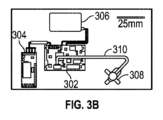
図3Aは、対象により着用可能である、例示的な呼びかけ機のブロック図を表す。前記呼びかけ機は、無線通信システム(図中では、Bluetooth(登録商標)無線)を含む。前記無線通信システムは、コンピュータシステムとの通信のために用いられてよい。図3Bは、着用可能な呼びかけ機の分解図を表す。前記呼びかけ機は、バッテリ、無線通信システム、およびトランスデューサアレイを含む。図3Cは、対象へ取り付けるためのハーネスを付けて完全に組み立てた、図3Bで示した着用可能な呼びかけ機を表す。図3Dは、対象、すなわちげっ歯類(ただし、ヒト、イヌ、ネコ、ウマ、ウシ、ブタ、ヒツジ、ヤギ、ニワトリ、サル、ラット、マウス等、任意の動物であってよい)に取り付けられた、着用可能な呼びかけ機を示す。前記呼びかけ機は、トランスデューサアレイを含む。前記トランスデューサアレイは、接着材で対象の体に固定される。図3Eは、図3A~図3Dで示した呼びかけ機のトランスデューサアレイの断面図を示す。 FIG. 3A depicts a block diagram of an exemplary interrogator wearable by a subject. The interrogator includes a wireless communication system (a Bluetooth® radio in the figure). The wireless communication system may be used for communication with computer systems. FIG. 3B depicts an exploded view of the wearable interrogator. The interrogator includes a battery, a wireless communication system, and a transducer array. FIG. 3C depicts the wearable interrogator shown in FIG. 3B fully assembled with a harness for attachment to a subject. Figure 3D was attached to a subject, a rodent (but can be any animal, such as humans, dogs, cats, horses, cows, pigs, sheep, goats, chickens, monkeys, rats, mice, etc.). , indicating a wearable interrogator. The interrogator includes a transducer array. The transducer array is secured to the subject's body with an adhesive. FIG. 3E shows a cross-sectional view of the transducer array of the interrogator shown in FIGS. 3A-3D.
図4は、呼びかけ機中のトランスデューサと、小型化超音波トランスデューサを有する埋め込み型デバイスとの間の通信を表す概略図である。前記呼びかけ機は、埋め込み型デバイスへ超音波を送信し、小型化超音波トランスデューサは、センサによって変調された超音波後方散乱を発する。そして、呼びかけ機が後方散乱を受信する。 FIG. 4 is a schematic diagram representing communication between a transducer in an interrogator and an implantable device having a miniaturized ultrasound transducer. The interrogator transmits ultrasound to the implantable device and a miniaturized ultrasound transducer emits ultrasound backscatter modulated by the sensor. The interrogator then receives the backscatter.
図5Aは、呼びかけ機から発せられる超音波パルスの一連のサイクルを表す。呼びかけ機のトランシーバ基板が、前記呼びかけ機(例えば、FPGA)からのトリガーを受信すると、一連の送信パルスを発生させる。送信サイクルの最後に、ASIC上のスイッチは、送信モジュールとの接続を絶ち、受信モジュールと接続する。各サイクルは、100マイクロ秒である。図5Bは、図5Aで示した送信パルスシーケンス(つまり、1サイクル)の拡大図を表す。前記サイクルにおいて、1.85MHzの超音波パルスが6つ存在し、前記超音波パルスは、540ナノ秒毎に繰り返し発生する。図5Cは、埋め込み型デバイスから発せられる超音波後方散乱を示す。超音波後方散乱は、約2tレイリーで呼びかけ機のトランスデューサに届く。図5Dは、超音波後方散乱の拡大図を示し、該超音波後方散乱は分析可能である。超音波後方散乱の分析は、超音波後方散乱波のフィルタリング工程、整流化工程、および積分工程を含む。図5Eは、フィルタリングされた超音波後方散乱波の拡大図を示す。前記後方散乱波は、小型化超音波トランスデューサへのインピーダンスの変化に応答する応答領域と、小型化超音波トランスデューサへのインピーダンスの変化に応答しない非応答領域とを含む。 FIG. 5A represents a series of cycles of ultrasonic pulses emitted from the interrogator. When the interrogator's transceiver board receives a trigger from the interrogator (eg, FPGA), it generates a series of transmit pulses. At the end of the transmit cycle, the switch on the ASIC disconnects from the transmit module and connects with the receive module. Each cycle is 100 microseconds. FIG. 5B represents an expanded view of the transmit pulse sequence (ie, one cycle) shown in FIG. 5A. In the cycle, there are six 1.85 MHz ultrasound pulses, which repeat every 540 ns. FIG. 5C shows ultrasonic backscatter emanating from an implantable device. Ultrasonic backscatter reaches the interrogator transducer in about 2t Rayleigh. FIG. 5D shows a magnified view of the ultrasonic backscatter, which can be analyzed. Analysis of ultrasonic backscatter includes filtering, rectification, and integration of the ultrasonic backscatter wave. FIG. 5E shows a magnified view of the filtered ultrasonic backscattered wave. The backscattered waves include responsive regions that respond to impedance changes to the miniaturized ultrasonic transducer and non-responsive regions that do not respond to impedance changes to the miniaturized ultrasonic transducer.
図6は、ASICに接続された小型化超音波トランスデューサ(「圧電素子」と称される)を有する埋め込み型デバイスの一実施形態を図示する。ASICは、電源回路、刺激回路(該刺激回路は、刺激電気パルスを発するよう、埋め込み型デバイスを作動させる)、および変調回路(または、「後方散乱回路」)を有する。電源回路は、エネルギー貯蔵コンデンサ(「cap」)を有する。電極は、組織中に埋め込まれ得る。 FIG. 6 illustrates one embodiment of an implantable device having a miniaturized ultrasound transducer (referred to as a "piezoelectric element") connected to an ASIC. The ASIC has power circuitry, stimulation circuitry (which activates the implantable device to emit stimulation electrical pulses), and modulation circuitry (or "backscatter circuitry"). The power supply circuit has an energy storage capacitor (“cap”). Electrodes may be embedded in tissue.
図7は、電気パルスを発するように構成されている埋め込み型デバイスの一実施形態を図示する。埋め込み型デバイスは、小型化超音波トランスデューサ、エネルギー貯蔵回路を備えている電源回路(上記エネルギー貯蔵回路は1つ以上のコンデンサ(「cap」を含み得る)、デジタル回路、および電極対を備える。 FIG. 7 illustrates one embodiment of an implantable device configured to emit electrical pulses. The implantable device comprises a miniaturized ultrasound transducer, a power circuit with an energy storage circuit (the energy storage circuit may include one or more capacitors (“cap”), a digital circuit, and an electrode pair.
図8Aは、プリント回路基板(PCB)上に小型化超音波トランスデューサおよびASICを含む、例示的な埋め込み型デバイスの概略図を示す。図8Bは、プリント回路基板(PCB)上に小型化超音波トランスデューサおよびASICを含む、別の例示的な埋め込み型デバイスの概略図を示す。 FIG. 8A shows a schematic diagram of an exemplary implantable device that includes a miniaturized ultrasound transducer and an ASIC on a printed circuit board (PCB). FIG. 8B shows a schematic diagram of another exemplary implantable device that includes a miniaturized ultrasound transducer and an ASIC on a printed circuit board (PCB).
図9は、本明細書中に記載の埋め込み型デバイスの製造方法を図解する。 FIG. 9 illustrates a method of manufacturing the implantable device described herein.
図10は、非晶質炭化珪素を含む埋め込み型デバイスの被包方法のフローチャートである。 FIG. 10 is a flowchart of a method for encapsulating an implantable device containing amorphous silicon carbide.
図11は、神経記録および神経刺激のための、クローズドループシステムを示す。電気生理学的パルスを検知するよう構成される1つ以上の埋め込み型デバイスは、外部のデバイス(上記外部のデバイスは、呼びかけ機を含む)に超音波後方散乱を送信する。超音波後方散乱は、電気生理学的パルスをエンコードする。そして、外部のデバイスは、電気パルスを発するよう構成される1つ以上の埋め込み型デバイスに、トリガー信号をエンコードする超音波を送信する。埋め込み型デバイスは、トリガー信号を受信した後、組織を刺激する電気パルスを発する。 FIG. 11 shows a closed loop system for neural recording and neural stimulation. One or more implantable devices configured to sense electrophysiological pulses transmit ultrasonic backscatter to an external device (the external device includes an interrogator). Ultrasound backscatter encodes electrophysiological pulses. The external device then transmits ultrasound waves encoding trigger signals to one or more implantable devices configured to emit electrical pulses. The implantable device emits electrical pulses that stimulate tissue after receiving a trigger signal.
図12は、小型化超音波トランスデューサと、電極対によって検知された電気生理学的信号に基づき、小型化超音波トランスデューサ中を流れる電流を変調するよう構成される変調回路とを備える、電気生理学的パルスを検知するよう構成される埋め込み型デバイスを図示する。 FIG. 12 illustrates an electrophysiological pulse comprising a miniaturized ultrasonic transducer and a modulating circuit configured to modulate the current flowing through the miniaturized ultrasonic transducer based on the electrophysiological signal sensed by the electrode pair. 1 illustrates an implantable device configured to detect a .
図13Aは、小型化超音波トランスデューサと、集積回路と、電極対とを備える、電気生理学的信号を検知するよう構成される埋め込み型デバイスを図示する。集積回路は、変調回路、AC複合増幅器列、および電源回路を備える。上記電源回路は、全波整流器および倍電圧器、レファレンスおよびレギュレータを備える。図13Bは、図13Aで示された集積回路において用い得る、例示的な整流器を図示する。図13Cは、図13Aで示された集積回路において用い得る、例示的な増幅器列を図示する。 FIG. 13A illustrates an implantable device configured to sense electrophysiological signals, comprising a miniaturized ultrasound transducer, an integrated circuit, and an electrode pair. The integrated circuit comprises a modulation circuit, an AC composite amplifier bank, and a power supply circuit. The power supply circuit includes a full wave rectifier and voltage doubler, a reference and a regulator. FIG. 13B illustrates an exemplary rectifier that can be used in the integrated circuit shown in FIG. 13A. FIG. 13C illustrates an exemplary amplifier bank that may be used in the integrated circuit shown in FIG. 13A.
図14Aは、埋め込み型デバイスの構成要素を接続するために使用する異なる形状のビアを示す。図14Bは、変形可能な相互接続用の、蛇行したトレース配置を示す。 FIG. 14A shows different shaped vias used to connect components of an implantable device. FIG. 14B shows a serpentine trace arrangement for a deformable interconnect.
図15は、銀エポキシを硬化させるための時間と温度の関係を示す。銀エポキシは、埋め込み型デバイスの製造においてワイヤボンドを取り付けるための材料の一例である。 FIG. 15 shows the relationship between time and temperature for curing the silver epoxy. Silver epoxy is one example of a material for attaching wire bonds in the manufacture of implantable devices.
図16は、埋め込み型デバイスを用いて記録された、神経電気記録図(ENG)を示す。点線は、グラウンドトルース電極によって記録された信号を示す。得られたデータから、複合活動電位を含む一般的な特徴が再構築された。前記一般的な特徴は、グラウンドトルースの特徴と一致する。 FIG. 16 shows neuroelectrograms (ENG) recorded using the implantable device. Dotted lines indicate the signal recorded by the ground truth electrode. From the data obtained, general features including compound action potentials were reconstructed. The general features match those of the ground truth.
図17は、埋め込み型デバイスを炭化珪素中に被包するための概略図を示す。 FIG. 17 shows a schematic diagram for encapsulating an implantable device in silicon carbide.
図18は、プロトタイプのアセンブリの概略とPCBを示す。 FIG. 18 shows the prototype assembly schematic and PCB.
図19A~Eは、所望の大きさの小型化超音波トランスデューサ(PZT)をPCB上に組み立てることを確実にするための処理工程を示す。図19Aにおいて、エポキシはんだペーストを基板上に配置する。図19Bにおいて、圧電材料をPCBに取り付ける。図19Cにおいて、圧電材料をダイシングし、所望のサイズのバルク圧電超音波トランスデューサを形成する。図19Dにおいて、超音波トランスデューサをPCBにワイヤボンディングする。図19Eにおいて、PCBおよび超音波トランスデューサをPDMS中に被包する。 Figures 19A-E show the processing steps to ensure assembly of the desired size miniaturized ultrasonic transducer (PZT) onto the PCB. In FIG. 19A, epoxy solder paste is placed on the substrate. In FIG. 19B, the piezoelectric material is attached to the PCB. In FIG. 19C, the piezoelectric material is diced to form bulk piezoelectric ultrasonic transducers of desired size. In FIG. 19D, the ultrasonic transducer is wirebonded to the PCB. In Figure 19E, the PCB and ultrasound transducer are encapsulated in PDMS.
図20は、ベクトルネットワークアナライザ(VNA)を用いた電気インピーダンス測定の概略図を示す。 FIG. 20 shows a schematic of electrical impedance measurements using a vector network analyzer (VNA).
図21Aは、異なる大きさのバルク圧電超音波トランスデューサにおいて測定された電力伝達効率が、シミュレートされた挙動と一致することを示す。図21Bは、測定されたPZT結晶のインピーダンス分光が、シミュレーションと一致することを示す。図21Cは、小型化超音波トランスデューサの得られた電力に対する周波数応答が、約6.1MHzであることを示す。 FIG. 21A shows that the measured power transfer efficiency in bulk piezoelectric ultrasonic transducers of different sizes agrees with the simulated behavior. FIG. 21B shows that the measured PZT crystal impedance spectroscopy agrees with the simulation. FIG. 21C shows that the frequency response to available power of the miniaturized ultrasonic transducer is approximately 6.1 MHz.
図22は、呼びかけ機の一部として使用することができる、例示的な超音波トランスデューサの概略図である。 FIG. 22 is a schematic diagram of an exemplary ultrasonic transducer that can be used as part of an interrogator.
図23は、電力送達の確認のための、校正済み超音波トランスデューサを用いた音響特徴付け設備の概略図である。超音波受信機は超音波送信機とは別個のものである。 FIG. 23 is a schematic diagram of an acoustic characterization setup using calibrated ultrasonic transducers for confirmation of power delivery. The ultrasonic receiver is separate from the ultrasonic transmitter.
図24Aは、ハイドロフォンをトランスデューサの表面から遠ざけたときの5MHzトランスデューサの出力を表す。図24Bは、軽減出力のピークが水におけるピークに比べて、左にシフトしていることを示す。 FIG. 24A represents the output of a 5 MHz transducer when the hydrophone is moved away from the surface of the transducer. FIG. 24B shows that the peak of the mitigation output is shifted to the left compared to the peak in water.
図25Aは、トランスデューサの出力のXZ断面図を示しており、レイリー距離と、近距離から遠距離への伝播の鮮明な変遷とを図示する。図25Bは、2.2mmのビームの6dBの帯域を示すXYビーム断面図を示す。 FIG. 25A shows an XZ cross section of the output of the transducer, illustrating the Rayleigh distance and the sharp transition of propagation from near to far range. FIG. 25B shows an XY beam cross section showing the 6 dB bandwidth of the 2.2 mm beam.
図26Aは、XY平面における、トランスデューサアレイからの集束された2次元ビームパターンを示す。測定されるビームは、X方向およびY方向の両方において、シミュレートされたビームに近接している。図26Bは、超音波トランスデューサアレイ中の各トランスデューサ素子に適用された遅延時間を示す。図26Cは、シミュレートされた2次元XZ断面のビームパターンを示す。 FIG. 26A shows a focused two-dimensional beam pattern from the transducer array in the XY plane. The measured beam is close to the simulated beam in both the X and Y directions. FIG. 26B shows the delay times applied to each transducer element in the ultrasound transducer array. FIG. 26C shows a simulated two-dimensional XZ cross-sectional beam pattern.
図27Aは、トランスデューサアレイから送信される超音波ビームのビームステアリングを示す。各ビームパターンの下は、図27Bに示すように、トランスデューサアレイ中の各トランスデューサが測定されたビームパターンを得るのに要する遅延である。図27Cは、図27Aで示したそれぞれのビームパターンの、X軸における1次元ビームパターンを示す。測定されたビームパターンは、シミュレートされたビームパターンに非常に近似している。 FIG. 27A shows beam steering of ultrasound beams transmitted from a transducer array. Below each beampattern is the delay required for each transducer in the transducer array to obtain the measured beampattern, as shown in FIG. 27B. FIG. 27C shows a one-dimensional beam pattern in the X-axis for each of the beam patterns shown in FIG. 27A. The measured beam pattern is very close to the simulated beam pattern.
図28は、組織中、5mmの送信距離における、シミュレートされた小型化超音波トランスデューサの連結効率および受信電力を示す。 FIG. 28 shows the coupling efficiency and received power of the simulated miniaturized ultrasound transducer at a transmit distance of 5 mm in tissue.
図29A~Dは、埋め込み型デバイスを有する、例示的なシステムの概要を示す。図29Aは、体内に局所的に配置された埋め込み型デバイスに電力を供給し、前記埋め込み型デバイスと通信する外部のトランスデューサを示す。カスタムされたトランシーバ基板によって駆動され、トランスデューサは、デバイスに電力を供給する一連のパルスの送信と、電気生理学的信号によって変調される反射されたパルスの受信とを交互に行う。図29Bは、麻酔されたラットの坐骨神経に固定された埋め込み型デバイスを示す。図29Bの挿入部分は、任意のテストリード線を有する埋め込み型デバイスを示す。図29Cは、例示的な埋め込み型デバイスの構成要素を示す。埋め込み型デバイスは、柔軟性のあるPCB上に組み立てられ、圧電性結晶、1つのカスタムされたトランジスタ、および記録電極対を有する。図29Dは、柔軟性のあるPCB上の、圧電性結晶上で得られた電子生理学的信号(グラウンドトルース)および電圧を測定するための校正リード線を有する、埋め込み型デバイスの拡大図を示す。インビボでの実験中は校正リード線を外した。 Figures 29A-D show an overview of an exemplary system having an implantable device. FIG. 29A shows an external transducer that powers and communicates with an implantable device placed locally within the body. Driven by a custom transceiver board, the transducer alternates between transmitting a series of pulses that power the device and receiving reflected pulses that are modulated by an electrophysiological signal. FIG. 29B shows an implantable device secured to the sciatic nerve of an anesthetized rat. The inset of FIG. 29B shows the implantable device with optional test leads. FIG. 29C shows components of an exemplary implantable device. The implantable device is assembled on a flexible PCB and has a piezoelectric crystal, one custom transistor and a pair of recording electrodes. FIG. 29D shows an enlarged view of the implantable device on a flexible PCB with calibration leads for measuring electrophysiological signals (ground truth) and voltages obtained on the piezoelectric crystal. The calibration leads were disconnected during the in vivo experiments.
図30は、例示的な呼びかけ機および埋め込み型デバイス間の通信を図示する。図30の上部は、情報の流れの概略図である。図30の下部は、図の上部に示される図解で表される各ステップにおける、信号の時間経過を表す。図30Aでは、呼びかけ機からのFPGAが、記録開始のトリガー信号を発生する。図30Bは、埋め込み型デバイス上の記録電極に送られた細胞外電気生理学的電位を示す。図30Cは、FPGAからのトリガーを受信する際、トランシーバ基板が一連の送信パルスを発生させることを示す。送信サイクルの最後には、呼びかけ機のASIC上のスイッチは、送信モジュールとの接続が断たれ、受信モジュールと接続される。図30Dは、1.85MHzで、6パルスを示す、連続する送信パルスの拡大図を示す。図30Eは、埋め込み型デバイスからの後方散乱を示す。前記後方散乱は、約2tレイリー距離のトランスデューサまで到達する。図30Fは、後方散乱波形の拡大図を示す。後方散乱波形は、大きな飽和信号を含み、飽和信号の送信パルスとの重複は、電気的にフィードスルーし、無視される。後方散乱パルスが戻る際に、後方散乱パルスが送電窓に続いて確認され得る。図30Gは、フィルタリングされ、整流化された後方散乱波形、および波形を再構築するために計算された曲線下の領域を示す。図30Hは、10kHzでサンプリングされた、再構築された波形を示す。100μs毎に受信した、適切に反射されるパルスの曲線下の領域を算出することで、再構築された波形の各部を計算する。 FIG. 30 illustrates communication between an exemplary interrogator and an implantable device. The upper part of FIG. 30 is a schematic diagram of the information flow. The lower part of FIG. 30 represents the time course of the signal at each step represented by the diagram shown in the upper part of the figure. In Figure 30A, the FPGA from the interrogator generates the trigger signal to start recording. FIG. 30B shows extracellular electrophysiological potentials delivered to recording electrodes on the implantable device. FIG. 30C shows that the transceiver board generates a series of transmit pulses upon receiving a trigger from the FPGA. At the end of the transmit cycle, a switch on the interrogator ASIC disconnects from the transmit module and connects to the receive module. FIG. 30D shows a magnified view of successive transmitted pulses showing 6 pulses at 1.85 MHz. FIG. 30E shows backscattering from an implantable device. The backscatter reaches the transducer at about 2t Rayleigh distance. FIG. 30F shows a magnified view of the backscatter waveform. The backscatter waveform contains a large saturating signal, and the overlap of the saturating signal with the transmitted pulse electrically feeds through and is ignored. As the backscatter pulse returns, it can be seen following the transmission window. FIG. 30G shows the filtered and rectified backscatter waveform and the area under the curve calculated to reconstruct the waveform. FIG. 30H shows the reconstructed waveform sampled at 10 kHz. Each part of the reconstructed waveform is calculated by calculating the area under the curve of the well-reflected pulses received every 100 μs.
図31Aは、呼びかけ機トランスデューサの表面からの距離の関数としての、低減された正規化ピーク圧力が、1.85MHzの際、約8.9mmで低減された焦点を有することを示す。図31Bは、レイリー距離においてビームが集束していることを示す、近距離、レイリー距離、および遠距離における、XY断面のビームパターンおよびそれに対応するy=0のときの1次元電圧プロットを示す。図31Cは、トランスデューサの出力圧力は、入力電圧の一次関数であることを示す(最高32Vのピーク間電圧)。図31Dは、別の文脈において示した図5Eの再現)は、異なる領域で示される例示的な後方散乱波形である。後方散乱波形は、非応答領域から発生する反射に対応する領域によって(時間的に)両側を挟まれていることがわかる;これらの領域は、他のデバイスの構成要素から反射したパルスに対応している。非応答領域における測定を基準としてもよい。ここで、前記非応答領域は、生物学的データを読み込んだものではない。このように区別して測定を行うことで、実験における外部のトランスデューサに関するすべての構成の動作を、差し引くことができる。図31Eは、カスタムした水タンク設備から得られる校正曲線であり、ノイズフロアは0.18mVrmsであることを示す。図31Fは、ビームパターン出力の減退に続く、横への照準ミスの関数としてのノイズフロアの影響を示す。図31Gは、レイリー距離における、y=0のときのトランスデューサの軸外し電圧および出力低下の1次元のプロットを示す。図31Hは、角度の照準ミスに対する、低下のプロットを表す。角度の照準ミスによって、ビームパターンが歪む。つまり、ビームパターンが円ではなく、反対に長円形となる。これにより、焦点の半径が長くなる(そして、より広い範囲へとエネルギーが分散する)。つまり、焦点の歪みが、照準ミスにおける制約を緩和する。 FIG. 31A shows the reduced normalized peak pressure as a function of distance from the surface of the interrogator transducer with a reduced focus of about 8.9 mm at 1.85 MHz. FIG. 31B shows the beam pattern in the XY cross section and the corresponding one-dimensional voltage plots at y=0 at near, Rayleigh, and far distances, showing that the beam is focused at the Rayleigh distance. FIG. 31C shows that the output pressure of the transducer is a linear function of the input voltage (up to 32V peak-to-peak voltage). FIG. 31D is a reproduction of FIG. 5E shown in another context) is an exemplary backscatter waveform shown in different regions. It can be seen that the backscatter waveform is flanked (in time) by regions corresponding to reflections originating from non-responsive regions; these regions correspond to pulses reflected from other device components. ing. A measurement in a non-responsive region may be used as a reference. Here, the non-responsive region is not loaded with biological data. By making such a discrete measurement, the behavior of all configurations with respect to the external transducer in the experiment can be subtracted. FIG. 31E is a calibration curve obtained from a custom water tank installation showing a noise floor of 0.18 mV rms . FIG. 31F shows the effect of the noise floor as a function of lateral mis-pointing following beam pattern power decay. FIG. 31G shows a one-dimensional plot of transducer off-axis voltage and power drop at y=0 at Rayleigh distance. FIG. 31H represents a plot of falloff versus angular mis-aim. Angular mis-aiming distorts the beam pattern. In other words, the beam pattern is not circular, but elliptical. This increases the focal radius (and spreads the energy over a wider area). That is, focus distortion relaxes the constraint on mis-aim.
図32Aは、ラットの腓腹筋からEMGを記録するための、インビボにおける実験設備を示す。埋め込み型デバイスは、露出した筋肉表面上に配置され、傷口を外科縫合によって閉じた。外部のトランスデューサは超音波を埋め込み型デバイスとつなげ、無線データが記録され、コンピュータシステム(例えば、ラップトップコンピュータ)上に表示される。図32Bは、複数回の試験を通しての、グラウンドトルース測定と再構築されたEMG信号との比較を示す。20m秒のサンプルが記録され、刺激の間隔は6秒であった。図32Cは、記録されるEMG信号の電力スペクトル密度(PSD)を示す。当該電力スペクトル密度(PSD)は、グラウンドトルースおよび再構築されたダストデータそれぞれに対して、107Hzで4.32e4μV2/Hzおよび3.11e4μV2/Hzであり、波形の端により、いくつかの調波が見られた。図32Dは、t=0分、およびt=30分に記録された無線後方散乱データがR=0.901で一致したことを示す。 FIG. 32A shows an in vivo experimental set-up for recording EMG from the rat gastrocnemius muscle. The implantable device was placed over the exposed muscle surface and the wound was closed with surgical sutures. An external transducer couples the ultrasound waves to the implantable device and wireless data is recorded and displayed on a computer system (eg, laptop computer). FIG. 32B shows a comparison of ground truth measurements and reconstructed EMG signals over multiple trials. 20 ms samples were recorded and the inter-stimulus interval was 6 seconds. FIG. 32C shows the power spectral density (PSD) of the recorded EMG signal. The power spectral densities (PSDs) are 4.32e4 μV2/Hz and 3.11e4 μV2/Hz at 107 Hz for the groundtruth and reconstructed dust data, respectively, with waveform edges leading to several harmonics. seen. FIG. 32D shows that the radio backscatter data recorded at t=0 min and t=30 min were in agreement with R=0.901.
図33Aは、PCB上の電極を用いて刺激強度を変えてインビボで記録された、さまざまな強度のEMG信号を示す。図33Bは、埋め込み型デバイスを用いて、類似した勾配のEMG応答が無線に記録されたことを示す。図33Cは、グラウンドトルースおよび無線後方散乱データから再構築されたEMG信号が、応答飽和刺激振幅(response-saturating stimulation amplitude)(100%)の場合、R=0.795で一致した(54%、69%、77%、89%の場合、それぞれR=0.60、0.64、0.67、0.92で一致した)ことを示す。図33Dにおいて、定量的比較により、顕著な特徴との0.4mV未満の一致が示された。図33Eにおいて、EMGピーク間電圧は、刺激強度との予測されたS字形相関を示した。 FIG. 33A shows EMG signals of various intensities recorded in vivo using electrodes on the PCB with varying stimulation intensities. FIG. 33B shows that a similar gradient EMG response was recorded wirelessly using an implantable device. FIG. 33C shows EMG signals reconstructed from ground truth and radio backscatter data matched with R=0.795 for response-saturating stimulation amplitude (100%) (54%, 69%, 77%, and 89% agreed with R = 0.60, 0.64, 0.67, and 0.92, respectively). In FIG. 33D, quantitative comparison showed less than 0.4 mV agreement with the salient feature. In FIG. 33E, EMG peak-to-peak voltage showed the expected sigmoidal correlation with stimulus intensity.
図34Aは、PCB上の電極を用いて刺激強度を変えてインビボで記録された、さまざまな強度のENG信号を示す。図34Bは、モートを用いて、類似の勾配のENG応答が無線で記録されたことを示す。図34Cは、グラウンドトルースおよび無線後方散乱データから再構築されたENG信号が、応答飽和刺激振幅(response-saturating stimulation amplitude)(100%)の場合、R=0.886で一致した(44%、61%、72%、83%、89%の場合、それぞれR=0.822、0.821、0.69、0.918、0.87で一致した)ことを示す。図34Dにおいて、定量的比較により、顕著な特徴との0.2mV未満の一致が示された。図34Eにおいて、ENGピーク間電圧は、刺激強度との予測されたS字形相関を示した。 FIG. 34A shows ENG signals of various intensities recorded in vivo using electrodes on the PCB with varying stimulation intensities. FIG. 34B shows an ENG response of similar slope was recorded wirelessly using a mote. FIG. 34C shows ENG signals reconstructed from ground truth and radio backscatter data matched with R=0.886 for response-saturating stimulation amplitude (100%) (44%, 61%, 72%, 83% and 89% agreed with R=0.822, 0.821, 0.69, 0.918 and 0.87, respectively). In FIG. 34D, quantitative comparison showed less than 0.2 mV agreement with the salient features. In FIG. 34E, ENG peak-to-peak voltage showed the expected sigmoidal correlation with stimulus intensity.
図35Aは、異なる電極間隔におけるENG応答を、時間経過で記録したものを示す。図35Bは、様々な電極間隔におけるピーク間ENGを示す。 FIG. 35A shows the ENG response recorded over time at different electrode spacings. FIG. 35B shows the peak-to-peak ENG at various electrode spacings.
図36Aは、組織を模倣するために使用される超音波カップリングゲルに埋め込まれた埋め込み型デバイスを用いた、埋め込み型デバイスからの超音波後方散乱を示す。前記超音波散乱は、26マイクロ秒に集中する送信貫通および終了、および47マイクロ秒付近に集中する小型化超音波トランスデューサ後方散乱を含む。図36Bは、小型化超音波トランスデューサの後方散乱領域(応答領域)の拡大図である。これは、埋め込み型デバイスへの信号入力の結果、振幅が変調されることを示す。 FIG. 36A shows ultrasound backscatter from an implantable device with the implantable device embedded in an ultrasound coupling gel used to mimic tissue. The ultrasonic scatter includes transmit penetration and termination centered around 26 microseconds, and miniaturized ultrasonic transducer backscatter centered around 47 microseconds. FIG. 36B is an enlarged view of the backscatter area (response area) of the miniaturized ultrasonic transducer. This indicates that the signal input to the implantable device results in amplitude modulation.
図37は、単極でエンコードすることで、後方散乱の振幅パルスの変調により、埋め込み型デバイスから無線で得られる、ASCII文字「hello world」に対応するデジタルデータを示す。 FIG. 37 shows digital data corresponding to the ASCII characters “hello world” obtained wirelessly from the implantable device by modulating the backscattered amplitude pulse by unipolar encoding.
〔発明の詳細な説明〕
本明細書中に記載される埋め込み型デバイスは、該埋め込み型デバイスに電力を供給する超音波を受信するよう構成される小型化超音波トランスデューサ(小型化圧電トランスデューサ等)、エネルギー貯蔵回路を含む電源回路、および電気パルスを発するよう構成される2つ以上の電極を備える。また、埋め込み型デバイスは、電極を作動させるよう構成される、デジタル回路または混合信号集積回路を備え得る。埋め込み型デバイスは、電極を組織(神経組織、筋組織、または器官等)に取り付ける等して、対象に埋め込まれ得る。埋め込み型デバイスは、当該組織を刺激するために電気パルスを発し得る。小型化超音波トランスデューサは、呼びかけ機からの超音波エネルギーを受信する(該呼びかけ機は、外部にあっても、埋め込まれていてもよい)。該小型化超音波トランスデューサは、埋め込み型デバイスに電力を供給する。呼びかけ機は、埋め込み型デバイスに超音波を送信するよう構成される送信器を備える。いくつかの実施形態において、呼びかけ機は、受信器を備える。受信器は、複合トランシーバとして送信器と統合されていてもよく、受信器と送信機とが同一デバイス上に配置されているか、異なるデバイス上に配置されていてもよい。呼びかけ機から送信される超音波からの力学的エネルギーは、埋め込み型デバイス上の小型化超音波トランスデューサを振動させ、それにより、電流が発生する。電流からのエネルギーは、エネルギー貯蔵回路中に保存され得る。該エネルギー貯蔵回路は1つ以上のコンデンサを備え得る。呼びかけ機は、トリガー信号をエンコードし、超音波として埋め込み型デバイスに送信し得る。埋め込み型デバイスは、トリガー信号を受信した後、電気パルスを発する(例えば、エネルギー貯蔵回路に保存されるエネルギーのすべてまたは一部を放出することによる)。トリガー信号は、例えば、所定の信号として、またはその他のいくつかの信号(クローズドループシステムにおいて検知される電気生理学的信号等)に応答して、エンコードされ得る。埋め込み型デバイスは、デジタル回路を備え得、該デジタル回路は、エンコードされるトリガー信号を解読し、エネルギー貯蔵回路および電極が電気パルスを放出するように作動させるよう構成される。
[Detailed description of the invention]
The implantable devices described herein include a miniaturized ultrasound transducer (such as a miniaturized piezoelectric transducer) configured to receive ultrasound to power the implantable device, a power source including an energy storage circuit A circuit and two or more electrodes configured to emit an electrical pulse. Implantable devices may also include digital or mixed-signal integrated circuits configured to actuate the electrodes. An implantable device may be implanted in a subject, such as by attaching electrodes to tissue (such as neural tissue, muscle tissue, or an organ). Implantable devices can emit electrical pulses to stimulate the tissue. A miniaturized ultrasonic transducer receives ultrasonic energy from an interrogator (which may be external or embedded). The miniaturized ultrasound transducer powers the implantable device. The interrogator comprises a transmitter configured to transmit ultrasound to the implantable device. In some embodiments, the interrogator comprises a receiver. The receiver may be integrated with the transmitter as a combined transceiver, and the receiver and transmitter may be located on the same device or on different devices. Mechanical energy from ultrasound transmitted from the interrogator vibrates a miniaturized ultrasound transducer on the implantable device, thereby generating an electrical current. Energy from the current can be stored in an energy storage circuit. The energy storage circuit may comprise one or more capacitors. The interrogator may encode the trigger signal and transmit it as ultrasound to the implantable device. The implantable device emits an electrical pulse (eg, by releasing all or part of the energy stored in the energy storage circuit) after receiving the trigger signal. The trigger signal can be encoded, for example, as a predetermined signal or in response to some other signal, such as an electrophysiological signal sensed in a closed loop system. The implantable device may comprise digital circuitry configured to decode the encoded trigger signal and activate the energy storage circuitry and electrodes to emit electrical pulses.
埋め込み型デバイスまたは埋め込み型デバイスを形成する電極は、組織に埋め込まれ、刺激的な電気信号を発する。いくつかの実施形態において、組織は、神経組織(中枢神経系または末梢神経系における組織等)、筋組織(平滑筋、骨格筋、または心筋等)、または器官(大腸、小腸、胃、腎臓、分泌腺(唾液腺または乳腺等)または膀胱等)である。いくつかの実施形態において、組織への取り付けは、埋め込み型デバイスは組織を完全には囲まないように行われる。いくつかの実施形態において、埋め込み型デバイスは、組織上にあるか、組織に埋め込まれているか、または組織と接している。いくつかの実施形態において、埋め込み型デバイスの電極は、組織に取り付けられる。例えば、電極は、神経組織、筋組織、または器官上にあり得るか、または神経組織中に埋め込まれ得る(例えば、神経鞘を貫通することによる)。いくつかの実施形態において、1つ以上の電極は、カフス電極を備える。該カフス電極は、部分的に組織を囲み得る。いくつかの実施形態において、埋め込み型デバイスは組織の近くに配置され、電極が埋め込み型デバイスから広がり、組織に到達し得る。 Implantable devices or electrodes forming implantable devices are implanted in tissue and emit stimulating electrical signals. In some embodiments, the tissue is nerve tissue (such as tissue in the central or peripheral nervous system), muscle tissue (such as smooth muscle, skeletal muscle, or cardiac muscle), or organ (large intestine, small intestine, stomach, kidney, secretory glands (such as salivary or mammary glands) or bladder). In some embodiments, attachment to tissue is such that the implantable device does not completely surround the tissue. In some embodiments, the implantable device is on, embedded in, or in contact with tissue. In some embodiments, the electrodes of the implantable device are attached to tissue. For example, the electrodes can be on nerve tissue, muscle tissue, or an organ, or can be embedded in nerve tissue (eg, by penetrating the nerve sheath). In some embodiments, one or more electrodes comprise cuff electrodes. The cuff electrode may partially surround tissue. In some embodiments, the implantable device is placed near tissue and electrodes can extend from the implantable device to reach the tissue.
神経組織は、中枢神経系(脳(例えば、大脳皮質、大脳基底核、中脳、延髄、脳橋、視床下部、視床、小脳、脳外陰、または海馬)または脊髄等)の一部、または末梢神経系(体性神経または自律神経系における神経等)の一部である。例示的な神経として、坐骨神経、迷走神経、迷走神経枝、脛骨神経、脾神経(spenic nervie)、内臓神経、陰部神経、仙骨神経、眼窩上神経、および後頭神経が挙げられる。筋組織は、例えば、骨格筋、平滑筋、または心筋であり得る。例示的な筋肉として、腓腹筋、骨盤筋、胃平滑筋、および心筋が挙げられる。 Nerve tissue may be part of the central nervous system (such as the brain (e.g., cerebral cortex, basal ganglia, midbrain, medulla oblongata, pons, hypothalamus, thalamus, cerebellum, vulva, or hippocampus) or spinal cord), or peripheral Part of the nervous system (such as nerves in the somatic or autonomic nervous system). Exemplary nerves include the sciatic nerve, vagus nerve, vagal branch, tibial nerve, spenic nerve, splanchnic nerve, pudendal nerve, sacral nerve, supraorbital nerve, and occipital nerve. Muscle tissue can be, for example, skeletal muscle, smooth muscle, or cardiac muscle. Exemplary muscles include gastrocnemius muscle, pelvic muscle, gastric smooth muscle, and cardiac muscle.
本明細書中に記載される埋め込み型デバイスは、対象(すなわち、動物)に埋め込まれるか、または対象中において使用され得る。いくつかの実施形態において、対象は哺乳類である。例示的な対象として、げっ歯類(マウス、ラット、モルモット等)、ネコ、イヌ、ニワトリ、ブタ、ウシ、ウマ、ヒツジ、ウサギ、トリ、コウモリ、サル等が挙げられる。いくつかの実施形態において、対象はヒトである。 The implantable devices described herein can be implanted in or used in a subject (ie, an animal). In some embodiments, the subject is a mammal. Exemplary subjects include rodents (mice, rats, guinea pigs, etc.), cats, dogs, chickens, pigs, cows, horses, sheep, rabbits, birds, bats, monkeys, and the like. In some embodiments, the subject is human.
電気パルスは、例えば、手足を制御するため(すなわち、機能的電気刺激)、膀胱機能を制御するため、または睡眠時無呼吸または慢性関節リウマチを治療するために有用であり得る。例えば、Tracey, The inflammatory reflex, Nature vol. 420, pp. 853-859 (2002)を参照のこと。 Electrical pulses can be useful, for example, to control limbs (ie, functional electrical stimulation), to control bladder function, or to treat sleep apnea or rheumatoid arthritis. See, eg, Tracey, The inflammatory reflex, Nature vol. 420, pp. 853-859 (2002).
一般的に、近年、中枢神経系または末梢神経系における疾患の新しいクローズドループ神経調節治療パラダイムを発達させるための神経記録および神経刺激の使用への関心が高まっている。神経は、種々の標的器官に遠心性信号および求心性信号を伝達するため、効果的な技術として、複数の箇所からの記録および刺激に対する空間と時間における解決策が非常に必要とされている。加えて、これらの技術を臨床的に実現可能とするために、電位の影響および外部リード線または組織中のインプラントの微細な動きによる潜在的な感染および不都合な生体反応を避けるように、拘束しない必要がある。これらの問題に対処するために、本明細書中に記載されるのは、無線で、埋め込み型デバイスに電力を供給し、該埋め込み型デバイスと通信するための超音波後方散乱システムである。この技術の強みの1つは、従来のラジオ周波数技術と異なり、超音波によるシステムは、ミリメートルスケール、さらにはそれ以下に縮小可能であり、インプラントの深さが数センチメートル以上であっても確実に作動することである。これは、埋め込み型電子回路における、新しい技術への扉を開くだろう。 In general, there has been increasing interest in recent years in the use of neural recording and neural stimulation to develop new closed-loop neuromodulatory therapeutic paradigms for diseases in the central or peripheral nervous system. Since nerves carry efferent and afferent signals to various target organs, there is a great need for spatial and temporal solutions for recording and stimulation from multiple sites as an effective technique. Additionally, to make these techniques clinically feasible, they are unconstrained so as to avoid potential infection and adverse biological reactions due to electrical potential effects and micro-movements of external leads or implants in tissue. There is a need. To address these issues, described herein is an ultrasound backscatter system for wirelessly powering and communicating with an implantable device. One of the strengths of this technology is that, unlike traditional radio frequency techniques, ultrasound-based systems can be scaled down to the millimeter scale and even less, ensuring that implants can be several centimeters deep or more. is to operate This will open the door to new technologies in embedded electronics.
いくつかの実施形態において、上記システムは、中枢神経系または末梢神経系において、信号(例えば、電気生理学的信号)を記録、刺激、および/または妨害するために使用され得る。検知される電気生理学的信号は、神経刺激の標的(例えば、睡眠時無呼吸の治療、または糖尿病から慢性関節リウマチまでの広い範囲の新しい病気における膀胱機能の調節等)において、神経刺激標的のリアルタイムで神経力学についての詳細なフィードバックを提供することで、治療上の刺激のパラメータを誘発し、決定するために使用され得る。 In some embodiments, the system can be used to record, stimulate, and/or block signals (eg, electrophysiological signals) in the central or peripheral nervous system. Sensed electrophysiological signals are useful in real-time neurostimulation targets, such as treating sleep apnea or regulating bladder function in a wide range of emerging diseases from diabetes to rheumatoid arthritis. can be used to elicit and determine parameters of therapeutic stimulation by providing detailed feedback on neurodynamics.
さらに、本明細書中に開示されるのは、生体の重要なバイタルサインを連続的に監視することができるように数センチメートルの深さで組織中に埋め込まれる、ミリメートルスケール以下の埋め込み型センサに、無線で電力を供給し、該埋め込み型センサと通信するための方法である。 Further disclosed herein are sub-millimetre-scale implantable sensors that are implanted into tissue at depths of several centimeters to enable continuous monitoring of important vital signs of living organisms. and a method for wirelessly powering and communicating with the implantable sensor.
本明細書中に記載される埋め込み型デバイスは、従来の埋め込み型システムでは不可能であった深さで、電力が供給され、通信することができる。いくつかの実施形態において、電気生理学的信号を検知するよう構成される埋め込み型デバイスは、圧電トランスデューサ、特定用途向け集積回路(ASIC)、および記録電極対を備える。インプラントの一実施形態において、1つのバルク圧電トランスデューサを用い、さらに、記録用ASICまたは刺激用ASIC、および金電極を使用する。または、記憶する品質を改善するために、電極は、電気メッキを施した、または電気化学的蒸着を施したポリ(3,4-エチレンジオキシチオフェン)(PEDOT)、Pt、またはPtブラックであり得る。複数のこれらのモートを、所望の位置へ配置すること、またはモート上に複数の電極対を配置し、チップ上でマルチプレクサを使用することで、複数箇所での同時記録または複数箇所での同時刺激を実現することができる。異なる電極対からのデータは、振幅、周波数、または位相を変調された波形としてエンコードされ得る。 The implantable devices described herein can be powered and communicate at depths not possible with conventional implantable systems. In some embodiments, an implantable device configured to sense electrophysiological signals comprises a piezoelectric transducer, an application specific integrated circuit (ASIC), and a recording electrode pair. In one embodiment of the implant, one bulk piezoelectric transducer is used and a recording or stimulation ASIC and gold electrodes are used. Alternatively, the electrodes are electroplated or electrochemically deposited poly(3,4-ethylenedioxythiophene) (PEDOT), Pt, or Pt black to improve memory quality. obtain. Multiple of these motes can be placed at desired locations, or multiple pairs of electrodes can be placed on a mote and multiplexers can be used on the chip for simultaneous recording or stimulation at multiple locations. can be realized. Data from different electrode pairs can be encoded as amplitude, frequency, or phase modulated waveforms.
いくつかの実施形態において、超音波エネルギーを送信するため、または、ビームフォーミングアレイを使用して複数のモートに呼びかけるために、1つのトランスデューサを使用することで、外部のユニットが1つのモートに呼びかけることができる。ビームフォーミングアレイは、バルク圧電トランスデューサまたは容量性マイクロマシン超音波トランスデューサ(CMUT)、または圧電マイクロマシン超音波トランスデューサ(PMUT)に基づき得る。PMUTおよびCMUTは、半導体バッチ製造を用いて製造された、マイクロ電気機械的システム(MEMS)デバイスであり、各MUTは、受信する音波を送信することができる。 In some embodiments, an external unit interrogates a single mote using a single transducer to transmit ultrasonic energy or to interrogate multiple motes using a beamforming array. be able to. Beamforming arrays can be based on bulk piezoelectric transducers or capacitive micromachined ultrasonic transducers (CMUTs), or piezoelectric micromachined ultrasonic transducers (PMUTs). PMUTs and CMUTs are micro-electro-mechanical systems (MEMS) devices manufactured using semiconductor batch fabrication, each MUT being capable of transmitting acoustic waves that it receives.
いくつかの実施形態において、使用中において、埋め込み型デバイスは、標的神経上にあるか、標的神経周辺にあるか、または標的神経中にあり、電極側が標的神経と接している。重要な接続は、テスト部である10ミルのビアまで、直線、または蛇行のいずれかで伸びていてもよい。リード線の長さは、用途に応じて調節され得る。または、全体の大きさを小型化するために、構成要素は半分に分割され、電極に沿って、ボードの上部または下部のどちらかに組み立てられ得る。両面基板の組み立ては、ワイヤボンドやフリップチップボンディングする際に、ASICと圧電トランスデューサとの間が電気的および機械的に断絶される必要があるため、より複雑となり得る。 In some embodiments, in use, the implantable device is on, around, or in the target nerve with the electrode side in contact with the target nerve. The critical connection may extend either straight or serpentine to the 10 mil via that is the test section. The lead length can be adjusted depending on the application. Alternatively, to reduce overall size, the components can be split in half and assembled along the electrodes, either on the top or bottom of the board. Assembly of double-sided boards can be more complex due to the need for electrical and mechanical isolation between the ASIC and the piezoelectric transducer during wirebonding or flip-chip bonding.
いくつかの実施形態において、システムは、クローズドループ医学治療システムとして埋め込まれる。このようなシステムは、超音波を発生させ、かつ受信するよう構成される超音波トランシーバ、および全体的ではないが、神経構造を囲むように取り付けられる、埋め込み型デバイスの大きさの本体を含む。埋め込み型デバイスは、刺激用ASICを作動させるのに必要な電力を得るために、圧電トランスデューサおよびエネルギー貯蔵部を備える。埋め込み型デバイスは、刺激パルス発生回路、および神経構造を電気的に刺激、または妨害するために、刺激パルスを発生させるパルス発生回路と結合したリード線を備える。埋め込み型デバイスは、超音波トランシーバを介して、外部の装置と通信するための超音波後方散乱通信システムを、さらに備える。いくつかの実施形態において、システムは、以下のうち1つ以上を含んでもよい。(a)超音波トランシーバは、生体に埋め込まれるために構成されていてもよい。(b)システムは、超音波トランシーバと通信可能な、外部の装置を、さらに含んでいてもよい。(c)外部の装置は、超音波トランシーバと無線通信してもよい。(d)埋め込み型デバイスの本体は、さらに、生体状態を検知するよう構成され、検知された生体状態を示すデータを、外部の装置に通信してもよい。このような場合、外部の装置は、検知された生体状態データを分析し、分析によって特定された検知された生体状態データの場所である、埋め込み型デバイスと超音波通信を始めるよう構成される。これは、神経構造に電気的に刺激を与えたり、遮断したりするための刺激パルスを発生させるためである。いくつかの実施形態において、外部の装置は、生物学的状態を直接的に検知する。 In some embodiments, the system is implanted as a closed loop medical treatment system. Such a system includes an ultrasound transceiver configured to generate and receive ultrasound waves and a body the size of an implantable device that is mounted to surround, but not entirely, a neural structure. The implantable device includes piezoelectric transducers and energy storage to obtain the power necessary to operate the stimulation ASIC. The implantable device includes stimulation pulse generation circuitry and leads coupled to the pulse generation circuitry for generating stimulation pulses to electrically stimulate or disrupt neural structures. The implantable device further comprises an ultrasound backscatter communication system for communicating with external devices via the ultrasound transceiver. In some embodiments, the system may include one or more of the following. (a) The ultrasound transceiver may be configured to be implanted in a living body. (b) The system may further include an external device capable of communicating with the ultrasound transceiver. (c) An external device may wirelessly communicate with the ultrasound transceiver. (d) The body of the implantable device may be further configured to sense a biological condition and communicate data indicative of the sensed biological condition to an external device. In such cases, the external device is configured to analyze the sensed biostate data and initiate ultrasound communication with the implantable device that is the location of the sensed biostate data identified by the analysis. This is to generate stimulation pulses for electrically stimulating and blocking neural structures. In some embodiments, the external device directly senses the biological state.
いくつかの実施形態において、神経刺激システムは、神経構造に取り付けられ、全体的ではないが神経細胞を囲むよう構成される、埋め込み型デバイスの大きさの複数の本体を備え得る。埋め込み型デバイスの本体は、さらに、外部の装置と、デバイスの状態を示すデータを通信するよう構成されていてもよい。埋め込み型デバイスの本体は、外部の装置と、デバイスの動作を示すデータを通信するよう構成されていてもよい。加えて、埋め込み型デバイスの本体は、さらに、刺激パラメータを調節するためのフィードバックを提供するために、検知された生物学的状態を記録し、報告するよう構成されていてもよい。 In some embodiments, the neurostimulation system may comprise multiple bodies, the size of implantable devices, configured to attach to a neural structure and surround, but not entirely, a nerve cell. The body of the implantable device may also be configured to communicate data indicative of the state of the device with an external device. The body of the implantable device may be configured to communicate data indicative of the operation of the device with an external device. Additionally, the body of the implantable device may be further configured to record and report sensed biological conditions to provide feedback for adjusting stimulation parameters.
本明細書中に記載される埋め込み型デバイスの重要な利点は、無線で電力を供給されながら、対象の奥深くの神経組織または筋組織に、電気パルスを同時に発することができる点である。いくつかの実施形態において、埋め込み型デバイスは、クローズドループシステム中で作動し、検知された電気生理学的パルスに応答して、同時に電気パルスを発し得る。さらに、埋め込み型デバイスは、バッテリを充電する必要もなく、また、デバイス上に保存される情報を回収する必要もなく、長い間、対象中に保持され得る。 An important advantage of the implantable devices described herein is the ability to simultaneously deliver electrical pulses to nerve or muscle tissue deep within a subject while being wirelessly powered. In some embodiments, the implantable device can operate in a closed loop system and simultaneously emit electrical pulses in response to sensed electrophysiological pulses. Additionally, the implanted device can be kept in the subject for long periods of time without the need to recharge the battery or retrieve the information stored on the device.
電磁(EM)力伝達は、小さな埋め込み型デバイスに電力を供給するには実用的でない。なぜなら、組織およびそれらのエネルギーを得るのに必要とされる比較的大きな開口部(例えば、アンテナまたはコイル等)において力が減衰するからである。例えば、Seo et al., Neural dust: an ultrasonic, low power solution for chronic brain-machine interfaces, arXiv: 1307.2196v1 (July 8, 2013)を参照のこと。埋め込まれたデバイスへの十分な電力供給のためにEMを使用するには、インプラントを浅い位置に埋め込む必要があり、EM波が組織中を通って埋め込み型デバイスに到達するために、組織を余分に加熱する必要がある。EMとは反対に、超音波伝達は、組織内での電力の減衰が低い。これは、組織による超音波エネルギーの吸収量が比較的低く、(電磁波に比べて)超音波の波長が短いためである。さらに、超音波によって供給された波長が短いほど、電波よりも低い周波数でより高い空間分解能を示す。 Electromagnetic (EM) force transmission is impractical for powering small implantable devices. This is because the forces are attenuated in the tissues and the relatively large openings (eg, antennas or coils, etc.) required to capture their energy. See, for example, Seo et al., Neural dust: an ultrasonic, low power solution for chronic brain-machine interfaces, arXiv: 1307.2196v1 (July 8, 2013). The use of EM to sufficiently power the implanted device requires that the implant be implanted at a shallow depth, leaving too much tissue for the EM waves to travel through the tissue and reach the implanted device. must be heated to Contrary to EM, ultrasound transmission has low attenuation of power in tissue. This is due to the relatively low absorption of ultrasound energy by tissue and the short wavelength of ultrasound (compared to electromagnetic waves). Furthermore, the shorter wavelengths delivered by ultrasound offer higher spatial resolution at lower frequencies than radio waves.
超音波トランスデューサは、画像化、高強度集束超音波(HIFU)、物質の非破壊検査、スチールウォールを通しての通信および電力供給、水中通信、経皮的電力供給、およびエネルギー収集を含む、種々の分野における用途が発見されている。例えば、Ishida et al., Insole Pedometer with Piezoelectric Energy Harvester and 2 V Organic Circuits, IEEE J. Solid-State Circuits, vol. 48, no. 1, pp. 255-264 (2013)、Wong et al., Advantages of Capacitive Micromachined Ultrasonics Transducers (CMUTs) for High Intensity Focused Ultrasound (HIFU), IEEE Ultrasonics Symposium, pp. 1313-1316 (2007)、Ozeri et al., Ultrasonic Transcutaneous Energy Transfer for Powering Implanted Devices, Ultrasonics, vol. 50, no. 6, pp. 556-566 (2010)、およびRichards et al., Efficiency of Energy Conversion for Devices Containing a Piezoelectric Component, J. Micromech. Microeng., vol. 14, pp. 717-721 (2004)を参照のこと。電磁とは異なり、エネルギー伝達方法として超音波を使用することは、広く普及した民生的用途に含まれることはなく、しばしば見逃されていた。なぜなら、短距離で大きな開口部がある場合、電磁の効率の方が優れているからである。しかし、本明細書中で論じられる埋め込み型デバイスの大きさであって組織内にある場合、低音速であることで劇的に低い周波数による作動が可能であり、かつ、一般的に、組織中の音波のロスは、組織中の電磁の減衰よりも実質的に少ない。 Ultrasound transducers are used in a variety of fields, including imaging, high intensity focused ultrasound (HIFU), nondestructive inspection of materials, communication and power delivery through steel walls, underwater communication, transcutaneous power delivery, and energy harvesting. has been found to be used in For example, Ishida et al., Insole Pedometer with Piezoelectric Energy Harvester and 2 V Organic Circuits, IEEE J. Solid-State Circuits, vol. 48, no. 1, pp. 255-264 (2013), Wong et al., Advantages of Capacitive Micromachined Ultrasonics Transducers (CMUTs) for High Intensity Focused Ultrasound (HIFU), IEEE Ultrasonics Symposium, pp. 1313-1316 (2007), Ozeri et al., Ultrasonic Transcutaneous Energy Transfer for Powering Implanted Devices, Ultrasonics, vol. 50, 6, pp. 556-566 (2010), and Richards et al., Efficiency of Energy Conversion for Devices Containing a Piezoelectric Component, J. Micromech. Microeng., vol. 14, pp. 717-721 (2004). See also. Unlike electromagnetics, the use of ultrasound as an energy transfer method has never been included in widespread consumer applications and has often been overlooked. This is because electromagnetics are more efficient at short distances and with large apertures. However, at the size of the implantable devices discussed herein and within tissue, the low sound velocity allows for dramatically lower frequency actuation, and generally The loss of sound waves in is substantially less than the attenuation of electromagnetic waves in tissue.
超音波は比較的に低音速であることから、EMと比較して波長が実質的に短い。よって、同じ送信距離の場合、超音波システムは、遠距離においてより作動しやすく、そのために、EM送信器よりも広い空間を範囲とすることができる。さらに、組織中の音波のロスは、基本的に組織中の電磁の減衰よりも小さい。これは、音波の伝達が、組織の表面に変位電流を発生させる時間依存的な電場および/または磁場よりも、組織の圧縮や希薄化に依存しているためである。 Due to the relatively low sound velocity of ultrasound, the wavelength is substantially shorter than that of EM. Thus, for the same transmission distance, ultrasound systems are more likely to operate at long distances and, therefore, can cover more space than EM transmitters. Furthermore, the loss of sound waves in tissue is essentially less than the attenuation of electromagnetic waves in tissue. This is because sound wave transmission relies on tissue compression and rarefaction rather than time-dependent electric and/or magnetic fields that produce displacement currents at the tissue surface.
いくつかの実施形態において、埋め込み型デバイスに電力を供給することに加え、埋め込み型デバイスによって受信される超音波は、トリガー信号を含み得る。トリガー信号は、埋め込み型デバイス上の小型化超音波トランスデューサによって受信され、その後トランスデューサによって発生する電流としてエンコードされる。そして、信号はデジタル信号によって受信され、上記デジタル信号は、エネルギー貯蔵回路を作動させ、電極から組織に送信される電気パルスが放出され得る。トリガー信号は、ユーザオペレート入力信号のような入力信号に応答して、超音波によって送信され得るか、または、検知された電気生理学的信号に応答し得る。例えば、いくつかの実施形態において、トリガー信号は、埋め込み型デバイスによって検知された電気生理学的信号に応答して、呼びかけ機に送信される。 In some embodiments, in addition to powering the implantable device, ultrasound waves received by the implantable device may include a trigger signal. The trigger signal is received by a miniaturized ultrasound transducer on the implantable device and then encoded as a current generated by the transducer. A signal is then received by a digital signal, which activates an energy storage circuit that can emit an electrical pulse that is transmitted from the electrode to the tissue. The trigger signal may be ultrasonically transmitted in response to an input signal, such as a user-operated input signal, or may be in response to a sensed electrophysiological signal. For example, in some embodiments, trigger signals are sent to the interrogator in response to electrophysiological signals sensed by the implantable device.
いくつかの実施形態において、「ニューラルダスト」システムは、ニューラルダスト、または「モート」と称する、非常に小さな体内埋め込み型デバイスと、超音波送信およびモートから反射される後方散乱送信を用いて該モートのそれぞれと通信する埋め込み型超音波トランシーバと、該超音波トランシーバと無線通信する外部のトランシーバとを有する。「Seo et al., Neural dust: an ultrasonic, low power solution for chronic brain-machine interfaces, arXiv: 1307.2196v1 (July 8, 2013) (“Seo et al., 2013”)」、「Seo et al., Model validation of untethered, ultrasonic neural dust motes for cortical recording, J. Neuroscience Methods, vol. 244, pp. 114-122 (2014) (“Seo et al., 2014”)」、および「Bertrand et al., Beamforming approaches for untethered, ultrasonic neural dust motes for cortical recording: a simulation study, IEE EMBC, vol. 2014, pp. 2625-2628 (2014)」を参照のこと。これらの論文に記載されたニューラルダストシステムは、皮質記録(すなわち、脳の電気信号の記録)に用いられる。これらの論文に示された当該用途では、Seo et al., 2013の図1に示されるように、モートが脳組織(皮質)に埋め込まれ、超音波トランシーバが硬膜の下方、皮質上に埋め込まれ、外部のトランシーバが、患者の頭部の、硬膜下超音波トランシーバが埋め込まれた場所に近接する位置に設置される。 In some embodiments, the "neural dust" system uses very small implantable devices, called neural dust, or "motes," and ultrasonic transmissions and backscattered transmissions reflected from the motes to and an external transceiver in wireless communication with the ultrasound transceiver. "Seo et al., Neural dust: an ultrasonic, low power solution for chronic brain-machine interfaces, arXiv: 1307.2196v1 (July 8, 2013) (“Seo et al., 2013"), "Seo et al., Model validation of untethered, ultrasonic neural dust motes for cortical recording, J. Neuroscience Methods, vol. 244, pp. 114-122 (2014) (“Seo et al., 2014”)”, and “Bertrand et al., Beamforming "Approaches for untethered, ultrasonic neural dust motes for cortical recording: a simulation study, IEE EMBC, vol. 2014, pp. 2625-2628 (2014)". The neural dust system described in these papers is used for cortical recording (ie recording of electrical signals in the brain). In the applications presented in these papers, motes are implanted in brain tissue (cortex) and ultrasound transceivers are implanted above the cortex, below the dura, as shown in Figure 1 of Seo et al., 2013. and an external transceiver is placed on the patient's head in proximity to where the subdural ultrasound transceiver is implanted.
Seo et al., 2013およびSeo et al., 2014において、理論上、ニューラルダストシステムを、無線で神経データを記録するための小型のインプラント(ミリスケール以下)の開発のために使用することができることが示された。電気生理学的信号または電気パルスを用いた組織の刺激の正確な検出は、埋め込み型デバイスの位置または動きを正確に測定することで高められる。これにより、検出された信号を該信号を生成した組織に正確に帰すること、または、標的組織への正確な刺激、および、動きにより生じ得る信号をフィルタリングすることが確実に行われる。本明細書に記載されるように、埋め込み型デバイスの位置および動きを、非応答型超音波後方散乱を分析することで正確に測定することができる。さらに、埋め込み型デバイスは、超音波後方散乱にエンコードされたデジタル化信号を送信できることがわかっている。デジタル化信号により、電気生理学的信号検出(例えば、偽陽性信号をフィルタリングすることによる検出)の信頼性や、データ圧縮の信頼性が向上する(これは、例えば、埋め込み型デバイスが複数の電極を含む場合、特に有利となり得る)。また、複数の埋め込み型デバイスを使用する場合、または埋め込み型デバイスが複数の電極を含む場合、デジタル化信号により、超音波後方散乱中に固有の識別信号を含めることができる。 Seo et al., 2013 and Seo et al., 2014 that, in theory, neural dust systems can be used for the development of miniature implants (millimeter scale and below) for recording neural data wirelessly. It has been shown. Accurate detection of tissue stimulation with electrophysiological signals or electrical pulses is enhanced by accurately measuring the position or movement of the implantable device. This ensures accurate attribution of the detected signal to the tissue that generated it, or accurate stimulation of the target tissue and filtering of signals that may result from motion. As described herein, the position and motion of implantable devices can be accurately determined by analyzing non-response ultrasonic backscatter. Additionally, it has been found that implantable devices can transmit digitized signals encoded in ultrasound backscatter. The digitized signal improves the reliability of electrophysiological signal detection (e.g. detection by filtering false positive signals) and the reliability of data compression (e.g., when an implanted device uses multiple electrodes). can be particularly advantageous if included). Also, if multiple implantable devices are used, or if an implantable device includes multiple electrodes, the digitized signal can include a unique identification signal in the ultrasound backscatter.
存在する小型化、埋め込み型システムは、ワイヤで接続されており、これは、毎日の連用における問題を発生させたり、電磁による無線化の試みは、規定された安全な範囲内の電力レベルを維持しながら、ミリメートルスケール以下の埋め込み型デバイス、または組織中にセンチメートル以上の深さで埋め込まれた埋め込み型デバイスに電力を供給し、通信することを困難としたりする。従来技術と比較すると、本願のインプラントは、容易に製造、統合でき、過去には達せなかった寸法および深さにおいて可能なインプラントである点で優れている。 Existing miniaturized, implantable systems are hard-wired, which creates problems in daily use, and attempts to go wireless with electromagnetics are unable to maintain power levels within prescribed safe limits. However, it can make it difficult to power and communicate with sub-millimetre-scale implantable devices, or implanted at depths greater than a centimeter in tissue. Compared to the prior art, the implants of the present application are superior in that they are easily manufactured and integrated, allowing implants in previously unattainable dimensions and depths.
いくつかの実施形態において、埋め込み型デバイスは、クローズドループシステムにおいて、同一または異なる埋め込み型デバイスによって検知された状態(電気生理学的信号、温度、検体(例えば、イオン、グルコース、酸素等)の濃度、またはその他の分子(神経伝達物質、サイトカイン、ホルモン、その他の信号分子、またはタンパク質等)、pH、圧力、ひずみ、または生体インピーダンス等)に応答して、組織(筋組織、神経組織、または器官等)を刺激する。検知された状態は、局所的でも、全身でもあり得る。いくつかの実施形態において、電気生理学的信号を検知するよう構成される埋め込み型デバイスは、神経組織または筋組織に取り付けられ、神経電気図または筋電図を報告するために使用され得る。いくつかの実施形態において、埋め込み型デバイスは、生理学的状態に関する情報(温度、圧力、pH、または検体濃度等;(International Patent Application titled “IMPLANTS USING ULTRASONIC BACKSCATTER FOR SENSING PHYSIOLGOICAL CONDITIONS,” 出願日:2017年7月7日, Attorney Docket No. 416272012040を参照のこと)、または放射線または放射能標識された細胞および分子(International Patent Application titled “IMPLANTS USING ULTRASONIC BACKSCATTER FOR RADIATION DETECTION AND ONCOLOGY,” 出願日:2017年7月7日, Attorney Docket No. 416272012140を参照のこと)、組織中の電気インピーダンス(International Patent Application titled “IMPLANTS USING ULTRASONIC BACKSCATTER FOR SENSING ELECTRICAL IMPEDANCE OF TISSUE,” 出願日:2017年7月7日, Attorney Docket No. 416272012440を参照のこと)、および電気生理学的パルス(International Patent Application titled “IMPLANTS USING ULTRASONIC BACKSCATTER FOR DETECTING ELECTROPHYSIOLOGICAL SIGNALS,”出願日:2017年7月7日, Attorney Docket No. 416272012640を参照のこと))を検知および報告(超音波後方散乱を介して)するよう構成され得る。上述の文献は、本明細書中において、参照する目的でのみ援用される。 In some embodiments, the implantable device is used in a closed-loop system to detect conditions (electrophysiological signals, temperature, concentrations of analytes (e.g., ions, glucose, oxygen, etc.), or other molecules (such as neurotransmitters, cytokines, hormones, other signaling molecules, or proteins), pH, pressure, strain, or bioimpedance, etc.) in response to tissues (such as muscle tissue, nerve tissue, or organs). ). A detected condition can be local or systemic. In some embodiments, implantable devices configured to sense electrophysiological signals can be attached to nerve or muscle tissue and used to report electroneurograms or electromyograms. In some embodiments, the implantable device provides information regarding physiological conditions such as temperature, pressure, pH, or analyte concentration; July 7, Attorney Docket No. 416272012040) or radiation or radiolabeled cells and molecules (International Patent Application titled "IMPLANTS USING ULTRASONIC BACKSCATTER FOR RADIATION DETECTION AND ONCOLOGY," Filing Date: July 2017). July 7, Attorney Docket No. 416272012140), Electrical Impedance in Tissue (International Patent Application titled "IMPLANTS USING ULTRASONIC BACKSCATTER FOR SENSING ELECTRICAL IMPEDANCE OF TISSUE," Filing Date: July 7, 2017, Attorney Docket No. 416272012440), and electrophysiological pulses (see International Patent Application titled "IMPLANTS USING ULTRASONIC BACKSCATTER FOR DETECTING ELECTROPHYSIOLOGICAL SIGNALS," Filed July 7, 2017, Attorney Docket No. 416272012640). ) can be configured to detect and report (via ultrasonic backscatter). The documents mentioned above are incorporated herein by reference only.
〔定義〕
本明細書中に使用される場合、単数形(a、an、およびthe)は、文脈中で特に明記されていない場合、複数形を含む。
[Definition]
As used herein, the singular forms (a, an, and the) include plural forms unless the context clearly dictates otherwise.
本明細書中の値やパラメータにおける「約」とは、当該値およびパラメータ自体を対象としたばらつきを含む(かつ、意味する)。例えば、「約X」との記載は、「X」の記載を含む。 "About" any value or parameter herein includes (and means) variations directed to the value or parameter itself. For example, reference to "about X" includes reference to "X."
「小型化」なる用語は、最大寸法の長さが約5ミリメートル以下(例えば、約4mm以下、約3mm以下、約2mm以下、約1mm以下、または約0.5mm以下)である任意の材料または構成要素を表す。特定の実施形態において、「小型化」材料または「小型化」構成要素の最大寸法の長さは、約0.1mm~約5mm(例えば、約0.2mm~約5mm、約0.5mm~約5mm、約1mm~約5mm、約2mm~約5mm、約3mm~約5mm、または約4mm~約5mm)である。また、「小型化」は、体積が約5mm3以下(例えば、約4mm3以下、3mm3以下、2mm3以下、または1mm3以下)の任意の物質または構成要素を表すことができる。特定の実施形態において、「小型化」物質または「小型化」構成要素の体積は、約0.5mm3~約5mm3、約1mm3~約5mm3、約2mm3~約5mm3、約3mm3~約5mm3、または約4mm3~約5mm3である。 The term "miniaturized" refers to any material or Represents a component. In certain embodiments, the length of the largest dimension of the “miniaturized” material or “miniaturized” component is from about 0.1 mm to about 5 mm (eg, from about 0.2 mm to about 5 mm, from about 0.5 mm to about 5 mm, about 1 mm to about 5 mm, about 2 mm to about 5 mm, about 3 mm to about 5 mm, or about 4 mm to about 5 mm). Also, "miniaturized" can refer to any material or component having a volume of about 5 mm 3 or less (eg, about 4 mm 3 or less, 3 mm 3 or less, 2 mm 3 or less, or 1 mm 3 or less). In certain embodiments, the volume of the “miniaturized” material or “miniaturized” component is about 0.5 mm 3 to about 5 mm 3 , about 1 mm 3 to about 5 mm 3 , about 2 mm 3 to about 5 mm 3 , about 3 mm 3 to about 5 mm 3 , or from about 4 mm 3 to about 5 mm 3 .
「圧電トランスデューサ」は、圧電材料を含む超音波トランシーバの1種である。圧電材料は、水晶、セラミック、ポリマー、またはその他の任意の天然圧電材料もしくは合成圧電材料であってよい。 A "piezoelectric transducer" is a type of ultrasound transceiver that includes piezoelectric material. The piezoelectric material may be quartz, ceramic, polymer, or any other natural or synthetic piezoelectric material.
「非応答型」超音波は、検出信号から独立した反射率を有する超音波である。「非応答型リフレクタ」は、反射された波形が検出信号から独立するように超音波を反射する、埋め込み型デバイスの一構成要素である。 "Non-responsive" ultrasound is ultrasound that has a reflectance that is independent of the detected signal. A "non-responsive reflector" is a component of an implantable device that reflects ultrasound waves such that the reflected waveform is independent of the detected signal.
「対象」なる用語は、動物を表す。 The term "subject" refers to animals.
本明細書に記載の発明の各態様および各変形例は、各態様および各変形例から「構成される(consisting)」および/または「本質的に構成される(cosisting essentially of)」ことを含むと理解されたい。 Each aspect and variation of the invention described herein includes "consisting" and/or "consisting essentially of" each aspect and variation be understood.
値の範囲が示される場合、その範囲の上限値および下限値の間に介在する各値、および、記載された範囲内でその他に記載された値もしくは介在する値は、本開示の範囲に包含されることを理解されたい。記載された範囲が上限値または下限値を含む場合、これらの上限値および下限値を除外した範囲もまた、本開示に含まれる。 When a range of values is given, each intervening value between the upper and lower limits of that range, and any other stated or intervening value within the stated range, is encompassed within the disclosure. It should be understood that Where the stated range includes the upper or lower values, ranges excluding those upper and lower values are also included in the disclosure.
本明細書に記載される種々の実施形態における1つ以上またはすべての特性を組み合わせて、本発明の他の実施形態を形成してもよい。本明細書で使用される見出しは構成上のものであり、記載された発明の主題を限定すると解釈されるべきでない。 One or more or all features of the various embodiments described herein may be combined to form other embodiments of the invention. The headings used herein are organizational and should not be construed as limiting the subject matter described.
「実施形態」に関して上述した特徴および好ましい構成は、別個の好ましい構成であって、当該特定の実施形態のみに限定されるものではない。特徴および好ましい構成は、技術的に可能であれば、その他の実施形態の特徴と自由に組み合わせてよく、各特徴の好ましい組み合わせを形成してもよい。 The features and preferred configurations described above with respect to "embodiments" are separate preferred configurations and are not limited to only that particular embodiment. Features and preferred configurations may be freely combined with features of other embodiments, where technically possible, to form preferred combinations of each feature.
本明細書は、当業者が本発明を実施および使用できるようにするためのものであり、特許出願およびその各要件の文脈において提示される。記載される各実施形態に対する種々の変更は、当業者にとって容易に理解できるものであり、本明細書中の一般的原理をその他の実施形態に適用してもよい。そのため、本発明は示される実施形態に限定されることを意図しておらず、本明細書に記載の原理および特徴と一致する最も広い範囲を有すると認められるべきである。また、見出しは構成上のものであり、限定的なものと見なされるべきではない。最後に、本願に引用されるすべての特許文献および刊行物の開示は、すべての目的のため、参照により本明細書中に援用される。 This specification is to enable one skilled in the art to make and use the invention, and is presented in the context of the patent application and its respective requirements. Various modifications to each described embodiment will be readily apparent to those skilled in the art, and the general principles herein may be applied to other embodiments. As such, the present invention is not intended to be limited to the embodiments shown, but is to be viewed as having the broadest scope consistent with the principles and features described herein. Also, headings are organizational and should not be viewed as limiting. Finally, the disclosures of all patent documents and publications cited in this application are hereby incorporated by reference for all purposes.
〔呼びかけ機〕
呼びかけ機は、超音波を用いて、1つ以上の埋め込み型デバイスと無線通信することができる。超音波は、埋め込み型デバイスへ電力を供給し、かつ/または埋め込み型デバイスを作動させるために使用される。呼びかけ機によって発せられる超音波は、トリガー信号をエンコードすることができ、前記トリガー信号は、埋め込み型デバイスが電気パルスを発するよう合図する。呼びかけ機は、1つ以上の超音波トランスデューサを含む。超音波トランスデューサは、超音波送信器および/または超音波受診器(または、超音波を交替で送信または受信するよう構成され得るトランシーバ)として作動できる。1つ以上のトランスデューサは、トランスデューサアレイとして配置されてもよく、呼びかけ機は、任意で1つ以上のトランスデューサアレイを含んでもよい。いくつかの実施形態では、アレイ中の各トランスデューサは、規則的な間隔で配置されてもよく、不規則的な間隔で配置されてもよく、またはまばらに配置されてもよい。いくつかの実施形態では、アレイは柔軟性に富んでいる。いくつかの実施形態では、アレイは平面であり、いくつかの実施形態では、アレイは非平面である。いくつかの実施形態では、超音波送信機能は、別のデバイス上の超音波受信機能から分離されている。つまり、任意で、呼びかけ機は、埋め込み型デバイスへ超音波を送信する第1デバイス、および埋め込み型デバイスから超音波後方散乱を受信する第2デバイスを含む。
[caller]
The interrogator can wirelessly communicate with one or more implantable devices using ultrasound. Ultrasound is used to power and/or actuate implantable devices. Ultrasound waves emitted by the interrogator can encode a trigger signal, which signals the implantable device to emit an electrical pulse. The interrogator includes one or more ultrasonic transducers. An ultrasound transducer can act as an ultrasound transmitter and/or an ultrasound receiver (or a transceiver that can be configured to alternately transmit or receive ultrasound). The one or more transducers may be arranged as a transducer array and the interrogator may optionally include one or more transducer arrays. In some embodiments, each transducer in the array may be regularly spaced, irregularly spaced, or sparsely spaced. In some embodiments, arrays are flexible. In some embodiments the array is planar and in some embodiments the array is non-planar. In some embodiments, the ultrasound transmission functionality is separate from the ultrasound reception functionality on another device. Thus, optionally, the interrogator includes a first device that transmits ultrasound to the implantable device and a second device that receives ultrasound backscatter from the implantable device.
いくつかの実施形態において、呼びかけ機は、電気生理学的電圧を検知し、検知された電気的電圧信号を示す情報をエンコードする超音波後方散乱を発するよう構成される埋め込み型デバイスのような、埋め込み型デバイスからの超音波後方散乱を受信し得る。いくつかの実施形態において、呼びかけ機から発された超音波によってエンコードされ、電気パルスを送信するよう構成される埋め込み型デバイスによって受信されるトリガー信号は、検知された電気生理学的信号に関する情報をエンコードする受信された超音波後方散乱に応答して、送信される。 In some embodiments, the interrogator is an implantable device, such as an implantable device configured to sense electrophysiological voltages and emit ultrasonic backscatter that encodes information indicative of the sensed electrical voltage signals. may receive ultrasonic backscatter from the type device. In some embodiments, the trigger signal, encoded by ultrasound emitted from the interrogator and received by an implantable device configured to transmit electrical pulses, encodes information about the detected electrophysiological signal. is transmitted in response to received ultrasonic backscatter.
例示的な呼びかけ機を、図2Aに示す。図解される呼びかけ機は、複数の超音波トランスデューサを有するトランスデューサアレイを示す。いくつかの実施形態では、トランスデューサアレイは、1つ以上、2つ以上、3つ以上、5つ以上、7つ以上、10以上、15以上、20以上、25以上、50以上、100以上、250以上、500以上、1000以上、2500以上、5000以上、10,000以上またはより多くのトランスデューサを含む。いくつかの実施形態では、トランスデューサアレイは、100,000以下、50,000以下、25,000以下、10,000以下、5000以下、2500以下、1000以下、500以下、200以下、150以下、100以下、90以下、80以下、70以下、60以下、50以下、40以下、30以下、25以下、20以下、15以下、10以下、7つ以下、または5つ以下のトランスデューサを含む。トランスデューサアレイは、例えば、超音波トランスデューサピクセルを50以上含むチップであってもよい。図2Aに示される呼びかけ機は、1つのトランスデューサアレイを図解している。しかし、呼びかけ機は、1つ以上、2つ以上、または3つ以上の別個のアレイを含んでもよい。いくつかの実施形態では、呼びかけ機は、10以下のトランスデューサアレイ(例えば、9つ、8つ、7つ、6つ、5つ、4つ、3つ、2つ、または1つのトランスデューサアレイ)を含む。別個のトランスデューサアレイは、例えば、対象の異なる部分に配置することができ、かつ、同じ埋め込み型デバイス、または異なる埋め込み型デバイスと通信することができる。いくつかの実施形態では、トランスデューサアレイを、埋め込み型デバイスの両側に配置する。呼びかけ機は、ASICを含んでいてもよい。ASICは、トランスデューサアレイ中の各トランスデューサのためのチャネルを含む。いくつかの実施形態では、チャネルはスイッチを含む(図2A中、「T/Rx」として示される)。スイッチは、チャネルに接続されたトランスデューサを、超音波を送信または超音波を受信するよう交互に構成することができる。スイッチは、超音波受信回路を、より高電圧の超音波送信回路から絶縁することができる。いくつかの実施形態では、チャネルに接続されたトランスデューサは、超音波を受信するのみに構成されるか、または超音波を送信するのみに構成され、スイッチは任意でチャネルから省かれる。チャネルは、遅延制御部を含んでいてもよい。遅延制御部は、送信される超音波を制御するために作動する。遅延制御部は、例えば、位相シフト、時間遅延、パルス周波数、および/または波形(振幅および波長を含む)を制御することができる。遅延制御部は、レベルシフタに接続されていてもよい。レベルシフタは、遅延制御部からの入力パルスを、トランスデューサが超音波を送信するために用いるより高い電圧へとシフトさせる。いくつかの実施形態では、各チャネルにおいて波形および周波数を示すデータを、「波形表(wave table)」に保存してもよい。これにより、各チャネルにおける送信波形が異なっていてもよい。そして、遅延制御部およびレベルシフタを用いて、このデータを、トランスデューサアレイへ送る実際の送信信号へと「ストリーム」出力してよい。いくつかの実施形態では、各チャネルにおける送信波形が、マイクロコントローラまたはその他のデジタルシステムからの高速シリアル出力から直接的に生成され、レベルシフタまたは高電圧増幅器を介してトランスデューサ素子へ送られてもよい。いくつかの実施形態では、ASICは、ASICへ供給される第1電圧をより高電圧の第2電圧へ変換する、チャージポンプを含む(図2Aに図示)。第2電圧はチャネルへ印加される。チャネルを、遅延制御部を作動させるコントローラ(例えば、デジタルコントローラ)によって制御することができる。超音波受信回路において、受信された超音波は、(受信モードに設定された)トランスデューサによって電流へ変換され、該電流はデータ収集回路に送信される。いくつかの実施形態では、受信回路中に、(組織における損失を補うことができる)増幅器、アナログ・デジタル変換器(ADC)、可変利得増幅器(variable-gain-amplifier)または時間利得制御可変利得増幅器(time-gain-controlled variable-gain-amplifier)、および/またはバンドパスフィルタを含む。ASICは、電源から電力を引き込むことができる。電源の例はバッテリであり、これは、呼びかけ機が着用可能である実施形態で好ましい。図2Aに示す実施形態では、1.8Vの電源からASICへ電圧が供給され、チャージポンプによって32Vまで増大される。しかし、任意の適切な電圧を使用することができる。いくつかの実施形態では、呼びかけ機は、プロセッサおよび/または非一時的でコンピュータで読み取り可能な記憶装置を含む。いくつかの実施形態では、上述のチャネルは、T/Rxスイッチを含まないが、その代わりに独立したTx(送信)、および優れた飽和回復を有する低ノイズ増幅器の形態である高電圧Rx(受信回路)を有するRx(受信)を含む。いくつかの実施形態では、T/Rx回路は、サーキュレータを含む。いくつかの実施形態では、トランスデューサアレイは、呼びかけ機の送信回路/受信回路における処理チャネルよりも多くのトランスデューサ素子を含み、マルチプレクサが、パルス毎に異なる組の送信素子を選択する。例えば、64の送受信チャネルを、3:1マルチプレクサを介して、192の物理的トランスデューサ素子に接続し、任意のパルスに対して64のトランスデューサ素子のみが作動するようにする。 An exemplary interrogator is shown in FIG. 2A. The illustrated interrogator shows a transducer array having a plurality of ultrasonic transducers. In some embodiments, the transducer array is 1 or more, 2 or more, 3 or more, 5 or more, 7 or more, 10 or more, 15 or more, 20 or more, 25 or more, 50 or more, 100 or more, 250 Including 500 or more, 1000 or more, 2500 or more, 5000 or more, 10,000 or more or more transducers. In some embodiments, the transducer array is 100,000 or less, 50,000 or less, 25,000 or less, 10,000 or less, 5000 or less, 2500 or less, 1000 or less, 500 or less, 200 or less, 150 or less, 100 ≤ 90 or less, 80 or less, 70 or less, 60 or less, 50 or less, 40 or less, 30 or less, 25 or less, 20 or less, 15 or less, 10 or less, 7 or less, or 5 or less transducers. A transducer array may be, for example, a chip containing 50 or more ultrasound transducer pixels. The interrogator shown in FIG. 2A illustrates one transducer array. However, the interrogator may include one or more, two or more, or three or more separate arrays. In some embodiments, the interrogator uses 10 or fewer transducer arrays (e.g., 9, 8, 7, 6, 5, 4, 3, 2, or 1 transducer arrays). include. Separate transducer arrays, for example, can be placed in different portions of a subject and can communicate with the same implanted device or different implanted devices. In some embodiments, transducer arrays are placed on both sides of the implantable device. The interrogator may include an ASIC. The ASIC contains a channel for each transducer in the transducer array. In some embodiments, the channel includes a switch (denoted as "T/Rx" in Figure 2A). A switch can alternately configure a transducer connected to a channel to transmit ultrasound or receive ultrasound. The switch can isolate the ultrasound receive circuitry from the higher voltage ultrasound transmit circuitry. In some embodiments, a transducer connected to a channel is configured to only receive ultrasound or only to transmit ultrasound, and the switch is optionally omitted from the channel. A channel may include a delay control. A delay control operates to control the transmitted ultrasound. A delay control may control, for example, phase shift, time delay, pulse frequency, and/or waveform (including amplitude and wavelength). The delay controller may be connected to the level shifter. A level shifter shifts the input pulse from the delay control to a higher voltage that the transducer uses to transmit ultrasound. In some embodiments, data indicating waveforms and frequencies in each channel may be stored in a "wave table." Thereby, the transmission waveforms in each channel may be different. Delay controls and level shifters may then be used to "stream" this data out into the actual transmit signal that is sent to the transducer array. In some embodiments, the transmit waveform on each channel may be generated directly from a high speed serial output from a microcontroller or other digital system and sent to the transducer elements via level shifters or high voltage amplifiers. In some embodiments, the ASIC includes a charge pump (shown in FIG. 2A) that converts a first voltage supplied to the ASIC to a higher voltage second voltage. A second voltage is applied to the channel. The channels can be controlled by a controller (eg, a digital controller) that operates a delay control. In the ultrasound receiver circuit, the received ultrasound waves are converted by the transducer (set to receive mode) into electrical current, which is transmitted to the data acquisition circuit. In some embodiments, an amplifier (that can compensate for losses in tissue), an analog-to-digital converter (ADC), a variable-gain-amplifier, or a time-gain-controlled variable-gain amplifier is included in the receiver circuit. (time-gain-controlled variable-gain-amplifier), and/or a bandpass filter. An ASIC can draw power from a power supply. An example of a power source is a battery, which is preferred in embodiments where the interrogator is wearable. In the embodiment shown in FIG. 2A, voltage is supplied to the ASIC from a 1.8V power supply and boosted to 32V by a charge pump. However, any suitable voltage can be used. In some embodiments, the interrogator includes a processor and/or non-transitory computer-readable storage. In some embodiments, the channels described above do not include T/Rx switches, but instead have independent Tx (transmit) and high voltage Rx (receive) in the form of low noise amplifiers with excellent saturation recovery. circuit). In some embodiments, the T/Rx circuitry includes a circulator. In some embodiments, the transducer array includes more transducer elements than processing channels in the interrogator's transmit/receive circuitry, and a multiplexer selects a different set of transmit elements for each pulse. For example, 64 transmit and receive channels may be connected to 192 physical transducer elements via a 3:1 multiplexer so that only 64 transducer elements are active for any given pulse.
図2Bは、呼びかけ機の別の実施形態を示す。図2Bに示すように、呼びかけ機は、1つ以上のトランスデューサ202を含む。各トランスデューサ202は、送信/受信スイッチ204に接続されている。送信/受信スイッチ204は、トランスデューサが超音波を送信するように、または超音波を受信するように、交互に構成することができる。送信/受信スイッチは、プロセッサ206(例えば、中央演算処理装置(CPU)、カスタム専用処理プロセッサASIC、フィールドプログラマブルゲートアレイ(FPGA)、マイクロコントローラユニット(MCU)、またはグラフィック処理装置(GPU))に接続される。いくつかの実施形態では、呼びかけ機は、さらに、アナログ・デジタル変換器(ADC)またはデジタル・アナログ変換器(DAC)を含む。また、呼びかけ機は、ユーザインターフェース(ディスプレイや、呼びかけ機を制御する1つ以上のボタン等)、記憶装置、電源(バッテリ等)、および/または入出力ポート(有線であっても、無線であってもよい)を含んでもよい。 FIG. 2B shows another embodiment of an interrogator. As shown in FIG. 2B, the interrogator includes one or more transducers 202 . Each transducer 202 is connected to a transmit/receive switch 204 . The transmit/receive switch 204 can be alternately configured so that the transducer transmits ultrasound waves or receives ultrasound waves. The transmit/receive switch connects to a processor 206 (e.g., central processing unit (CPU), custom dedicated processor ASIC, field programmable gate array (FPGA), microcontroller unit (MCU), or graphics processing unit (GPU)). be done. In some embodiments, the interrogator further includes an analog-to-digital converter (ADC) or a digital-to-analog converter (DAC). The interrogator may also include a user interface (such as a display and one or more buttons that control the interrogator), storage, power (such as a battery), and/or input/output ports (whether wired or wireless). may include).
いくつかの実施形態では、呼びかけ機は埋め込み型である。埋め込み型デバイスが、容易に超音波を送信しない障害物によって妨害された領域に埋め込まれている場合は、埋め込まれた呼びかけ機が好ましいときもある。例えば、呼びかけ機は、頭蓋下(硬膜下または硬膜上)に埋め込まれてよい。頭蓋下の呼びかけ機は、脳内に埋め込まれた埋め込み型デバイスと通信することができる。超音波は頭蓋骨によって妨害されるため、頭蓋下に埋め込まれた呼びかけ機は、脳内に埋め込まれた埋め込み型デバイスと通信が可能である。別の実施例において、埋め込み型呼びかけ機は、別の埋め込み型デバイスまたは人工装具の一部またはその裏側もしくはその内部に埋め込むことができる。いくつかの実施形態において、埋め込まれた呼びかけ機は、例えばEMまたはRF信号によって、外部のデバイスとの通信および/または外部のデバイスによる電力の供給ができる。 In some embodiments, the interrogator is implantable. An embedded interrogator may be preferred if the implantable device is implanted in an area obstructed by an obstacle that does not readily transmit ultrasound. For example, the interrogator may be implanted subcranially (either subdurally or epidurally). A subcranial interrogator can communicate with an implantable device implanted in the brain. Because ultrasound waves are blocked by the skull, interrogators implanted under the skull can communicate with implantable devices implanted in the brain. In another example, the implantable interrogator can be embedded within or behind or within part of another implantable device or prosthesis. In some embodiments, the implanted interrogator can communicate with and/or be powered by an external device, eg, by EM or RF signals.
いくつかの実施形態では、呼びかけ機は外部の(つまり、埋め込まれていない)呼びかけ機であってよい。一実施例として、外部の呼びかけ機は着用可能であり得、ストラップまたは接着材で身体に固定してよい。別の実施例において、外部の呼びかけ機は、棒状であり得、ユーザ(医療従事者等)によって保持されてよい。いくつかの実施形態では、呼びかけ機を、縫合糸、簡単な表面張力、風呂敷のような被服における固定器具、スリーブ、ゴムバンド、または、皮下固定を介して身体に保持させることができる。呼びかけ機のトランスデューサまたはトランスデューサアレイは、残りのトランスデューサから離れて配置されてもよい。例えば、トランスデューサアレイを対象の皮膚の第1位置(1つ以上の埋め込み型デバイスに近接した位置等)に固定することができ、そして、呼びかけ機の残りを第2位置に配置し、トランスデューサまたはトランスデューサアレイを、呼びかけ機の残りとワイヤでつないでもよい。図3A~図3Eは、着用可能な外部の呼びかけ機の例を示す。図3Aは呼びかけ機のブロック図を示し、当該呼びかけ機は、複数のトランスデューサを含むトランスデューサアレイと、当該トランスデューサアレイ中の各トランスデューサ用のチャネルを含むASICと、バッテリ(図示された実施例では、リチウムポリマーバッテリ(LiPo))と、無線通信システム(Bluetooth(登録商標)システム等)とを有する。図3Bは着用可能な呼びかけ機の分解図を示し、当該着用可能な呼びかけ機は、プリント回路基板(PCB)302(ASICを含む)と、無線通信システム304と、バッテリ306と、超音波トランスデューサアレイ308と、ワイヤ310(超音波トランスデューサアレイ308をASICにつないでいる)とを有する。図3Cは、図3Bに示す着用可能な呼びかけ機312にハーネス314を取り付けた状態を示し、当該ハーネス314は呼びかけ機を対象に取り付けるために使用できる。図3Dは、組み立てられ、対象に取り付けられた呼びかけ機316を示し、トランスデューサアレイ308を第1位置に取り付け、呼びかけ機の残りを第2位置に取り付けてある。図3Eは例示的な超音波トランスデューサアレイ308の断面概略図を示し、当該超音波トランスデューサアレイ308は、回路基板318と、各トランスデューサ322を回路基板318に取り付けているビア320と、金属化ポリエステルフィルム324と、吸収性支持体層326とを有する。金属化ポリエステルフィルム324は、各トランスデューサに対して共通の土台となり音響的に整合しており、一方、吸収性支持体層326(タングステン粉末を注入したポリウレタン等)は、個々のトランスデューサの共鳴を低減させることができる。
In some embodiments, the interrogator may be an external (ie, non-embedded) interrogator. As one example, the external interrogator may be wearable and secured to the body with a strap or adhesive. In another example, the external interrogator may be bar-shaped and held by a user (such as a healthcare worker). In some embodiments, the interrogator can be held to the body via sutures, simple surface tension, fasteners in clothing such as furoshiki, sleeves, elastic bands, or subcutaneous fasteners. The interrogator transducer or transducer array may be spaced apart from the rest of the transducers. For example, a transducer array can be secured to a subject's skin at a first location (such as in proximity to one or more implantable devices), and the rest of the interrogator is placed at a second location, the transducer or transducers The array may be wired to the rest of the interrogator. Figures 3A-3E show examples of wearable external interrogators. FIG. 3A shows a block diagram of an interrogator comprising a transducer array containing multiple transducers, an ASIC containing a channel for each transducer in the transducer array, a battery (lithium a polymer battery (LiPo)) and a wireless communication system (such as a Bluetooth® system). FIG. 3B shows an exploded view of a wearable interrogator comprising a printed circuit board (PCB) 302 (including an ASIC), a
トランスデューサアレイの特定の設計は、所望の侵入深度、開口部の大きさ、およびトランスデューサアレイ中のトランスデューサの大きさに依存する。トランスデューサアレイのレイリー距離「R」は、下記式で計算される。 The particular design of the transducer array depends on the desired penetration depth, aperture size, and size of the transducers in the transducer array. The Rayleigh distance "R" of the transducer array is calculated by the following equation.

式中、Dは開口部の大きさであり、λは伝播媒体(すなわち、組織)中の超音波の波長である。当該技術分野において理解されるように、レイリー距離はトランスデューサアレイによって放射されるビームが完全に形成される距離である。つまり、受信される電力を最大限にするために、加えられた圧力は、レイリー距離の自然焦点に集束する。そのため、いくつかの実施形態では、埋め込み型デバイスのトランスデューサからの距離は、およそレイリー距離と同じである。 where D is the aperture size and λ is the wavelength of ultrasound in the propagation medium (ie, tissue). As understood in the art, the Rayleigh distance is the distance over which the beam emitted by the transducer array is completely formed. That is, the applied pressure is focused to the natural focus of the Rayleigh distance to maximize the received power. Therefore, in some embodiments, the distance from the transducer of the implantable device is approximately the Rayleigh distance.
トランスデューサアレイ中の個々のトランスデューサを変調して、当該トランスデューサアレイによって発せられる超音波のビームのレイリー距離および位置を、ビームフォーミングまたはビームステアリングのプロセスにより制御することができる。線形拘束付最小分散型(LCMV)ビームフォーミングのような技術を用いて、複数の埋め込み型デバイスを外部の超音波トランシーバと通信させることができる。例えば、Bertrand et al., Beamforming Approaches for Untethered, Ultrasonic Neural Dust Motes for Cortical Recording: a Simulation Study, IEEE EMBC (Aug. 2014)を参照のこと。いくつかの実施形態では、ビームステアリングは、トランスデューサアレイ中のトランスデューサから発せられる超音波の出力または位相を調整することで行われる。 Individual transducers in a transducer array can be modulated to control the Rayleigh distance and position of the beam of ultrasound emitted by the transducer array through a process of beamforming or beam steering. Techniques such as linear constrained minimum variance (LCMV) beamforming can be used to allow multiple implanted devices to communicate with an external ultrasound transceiver. See, for example, Bertrand et al., Beamforming Approaches for Untethered, Ultrasonic Neural Dust Motes for Cortical Recording: a Simulation Study, IEEE EMBC (Aug. 2014). In some embodiments, beamsteering is accomplished by adjusting the power or phase of ultrasound waves emitted from transducers in a transducer array.
いくつかの実施形態では、呼びかけ機は、1つ以上のトランスデューサを用いて超音波をビームステアリングする命令、1つ以上の埋め込み型デバイスの相対的位置を特定する命令、1つ以上の埋め込み型デバイスの相対的移動を監視する命令、1つ以上の埋め込み型デバイスの相対的移動を記録する命令、および複数の埋め込み型デバイスからの後方散乱をデコンヴォルーションする命令のうち1つ以上を有する。 In some embodiments, the interrogator provides instructions to beamsteer ultrasound using one or more transducers, instructions to identify relative positions of one or more implantable devices, instructions to monitoring relative movement of the implantable devices, recording relative movement of one or more implantable devices, and deconvolving backscatter from multiple implantable devices.
〔埋め込み型デバイスおよび呼びかけ機間の通信〕
埋め込み型デバイスおよび呼びかけ機は、超音波を用いて、無線で相互通信する。埋め込み型デバイスは、埋め込み型デバイス上の小型化超音波トランスデューサを介して、呼びかけ機からの超音波を受信する。埋め込み型デバイス上の小型化超音波トランスデューサの振動によって、トランスデューサの電気端子間における電圧が発生し、(もし存在するならば、集積回路を備える)埋め込み型デバイス中に電流が流れる。電流は、エネルギー貯蔵回路に電流を供給するために使用され、上記エネルギー貯蔵回路は、例えば、トリガー信号を受信した後に、電気パルスを発するために使用されるエネルギーを貯蔵し得る。トリガー信号は、呼びかけ機から埋め込み型デバイスに送信され、電気パルスを発するよう信号を送る。いくつかの実施形態において、トリガー信号は、周波数、振幅、パルス波長、またはパルス波形(例えば、交流、電流の向き、またはパルスパターン等)のような、発せられる電気パルスに関する情報を含む。デジタル回路は、トリガー信号を解読し、電極および電気貯蔵回路がパルスを発するように作動させることができる。
[Communication between implantable device and interrogator]
The implantable device and interrogator wirelessly communicate with each other using ultrasound. The implantable device receives ultrasound from the interrogator via a miniaturized ultrasound transducer on the implantable device. Vibration of a miniaturized ultrasound transducer on the implantable device produces a voltage across the electrical terminals of the transducer, causing current to flow through the implantable device (including the integrated circuit, if present). The current is used to supply current to an energy storage circuit, which may store energy that is used to emit the electrical pulse, for example after receiving a trigger signal. A trigger signal is sent from the interrogator to the implantable device, signaling it to emit an electrical pulse. In some embodiments, the trigger signal includes information about the emitted electrical pulse, such as frequency, amplitude, pulse wavelength, or pulse shape (eg, alternating current, current direction, pulse pattern, etc.). A digital circuit can decode the trigger signal and activate the electrodes and electrical storage circuit to pulse.
いくつかの実施形態において、超音波後方散乱は、埋め込み型デバイスから発せられ、前記後方散乱は、埋め込み型デバイスまたは埋め込み型デバイスから発せられる電気パルスに関する情報をエンコードすることができる。例えば、超音波後方散乱は、確認信号をエンコードすることができ、前記確認信号は、電気パルスがどこから発せられたかを検証する。いくつかの実施形態において、埋め込み型デバイスは、電気生理学的信号を検知するよう構成される。そして、検知される電気生理学的信号に関する情報は、超音波後方散乱によって、呼びかけ機に送信され得る。超音波後方散乱に信号をエンコードするために、小型化超音波トランスデューサ中を流れる電流は、検知される電気生理学的信号のような、エンコードされる情報の関数として変調される。いくつかの実施形態において、電流の変調は、アナログ信号であってもよく、前記アナログ信号は、例えば、検知された電気生理学的信号によって直接的に変調されてもよい。いくつかの実施形態において、電流の変調は、デジタル化信号をエンコードし、前記デジタル化信号は、集積回路におけるデジタル回路によって制御されてもよい。後方散乱は、外部の超音波トランシーバ(最初の超音波を送信した外部の超音波トランシーバと同じであっても異なっていてもよい)によって受信される。このように、電気生理学的信号からの情報を、後方散乱超音波の振幅、周波数、または位相の変化によってエンコードすることができる。 In some embodiments, ultrasonic backscatter emanates from an implantable device, and said backscatter can encode information about the implantable device or electrical pulses emanating from the implantable device. For example, ultrasonic backscatter can encode a confirmation signal, which verifies where the electrical pulse originated from. In some embodiments, the implantable device is configured to sense electrophysiological signals. Information about the sensed electrophysiological signals can then be transmitted to the interrogator by ultrasonic backscatter. To encode a signal into ultrasonic backscatter, the current flowing through the miniaturized ultrasonic transducer is modulated as a function of the information to be encoded, such as the electrophysiological signal to be sensed. In some embodiments, the current modulation may be an analog signal, which may be modulated directly by, for example, the sensed electrophysiological signal. In some embodiments, the current modulation encodes a digitized signal, and said digitized signal may be controlled by digital circuitry in an integrated circuit. The backscatter is received by an external ultrasound transceiver (which may be the same or different than the external ultrasound transceiver that transmitted the original ultrasound). Thus, information from the electrophysiological signal can be encoded by changes in the amplitude, frequency, or phase of the backscattered ultrasound waves.
図4は、埋め込み型デバイスと通信する呼びかけ機を示す。外部の超音波トランシーバは超音波(「搬送波」)を発し、当該超音波は組織を通過することができる。前記搬送波は、小型化超音波トランスデューサ(例えば、小型化バルク圧電トランスデューサ、PUMT、またはCMUT)上で機械的振動を発生させる。小型化超音波トランスデューサで電圧が発生し、それにより、埋め込み型デバイス上の集積回路に電流が流れる。小型化超音波トランスデューサ中へと流れる電流によって、埋め込み型デバイス上のトランスデューサから後方散乱超音波が発せられる。いくつかの実施形態において、検出された電気生理学的信号は、直接的または間接的(集積回路を介して等)に小型化超音波トランスデューサ中を流れる電流を変調し、後方散乱波は、検出された電気生理学的信号に関する情報をエンコードする。後方散乱波は、呼びかけ機によって検出されることができ、前記後方散乱波を分析して、埋め込み型デバイスから検出された電気生理学的信号を見分けることができる。 FIG. 4 shows an interrogator communicating with an implantable device. An external ultrasound transceiver emits ultrasound waves (“carrier waves”) that can pass through tissue. The carrier waves generate mechanical vibrations on a miniaturized ultrasonic transducer (eg, miniaturized bulk piezoelectric transducer, PUMT, or CMUT). A voltage is generated at the miniaturized ultrasound transducer, which causes current to flow in integrated circuits on the implantable device. Current flowing into the miniaturized ultrasound transducer causes backscattered ultrasound waves to be emitted from the transducer on the implantable device. In some embodiments, the detected electrophysiological signal directly or indirectly (such as via an integrated circuit) modulates current flowing through the miniaturized ultrasound transducer, and the backscattered waves are detected. encodes information about the electrophysiological signal Backscattered waves can be detected by the interrogator, and the backscattered waves can be analyzed to discern electrophysiological signals detected from the implantable device.
呼びかけ機と埋め込み型デバイスとの間の通信は、超音波を送受信するパルス・エコー法を使用することができる。パルス・エコー法において、呼びかけ機は、所定の周波数の一連の呼びかけパルスを送信し、それから、埋め込み型デバイスから後方散乱エコーを受信する。いくつかの実施形態では、パルスの長さは、約200ナノ秒(ns)~約1000ns(例えば、約300ns~約800ns、約400ns~約600ns、または約540ns)である。いくつかの実施形態では、パルスの長さは、約100ns以上(例えば、約150ns以上、200ns以上、300ns以上、400ns以上、500ns以上、540ns以上、600ns以上、700ns以上、800ns以上、900ns以上、1000ns以上、1200ns以上、または1500ns以上)である。いくつかの実施形態では、パルスの長さは、約2000ns以下(例えば、1500ns以下、1200ns以下、1000ns以下、900ns以下、800ns以下、700ns以下、600ns以下、500ns以下、400ns以下、300ns以下、200ns以下、または150ns以下)である。いくつかの実施形態では、パルスは滞留時間によって分離される。いくつかの実施形態では、滞留時間の長さは、約100ns以上(例えば、約150ns以上、200ns以上、300ns以上、400ns以上、500ns以上、540ns以上、600ns以上、700ns以上、800ns以上、900ns以上、1000ns以上、1200ns以上、または1500ns以上)である。いくつかの実施形態では、滞留時間の長さは、約2000ns以下(例えば、約1500ns以下、1200ns以下、1000ns以下、900ns以下、800ns以下、700ns以下、600ns以下、500ns以下、400ns以下、300ns以下、200ns以下、または150ns以下)である。いくつかの実施形態では、パルスは、正方形、長方形、三角形、鋸歯状、または正弦である。いくつかの実施形態では、パルスの出力は、2段階(GNDおよびPOS)、3段階(GND、NEG、POS)、5段階、または他の任意の複数段階(例えば、24ビットDACを使用する場合)である。いくつかの実施形態では、パルスは、作動中に呼びかけ機から連続的に送信される。いくつかの実施形態では、パルスが呼びかけ機から連続的に送信される場合、呼びかけ機上のトランスデューサの一部は、超音波を受信するよう構成されており、呼びかけ機上のトランスデューサの一部は超音波を送信するように構成されている。超音波を受信するよう構成されたトランスデューサと、超音波を送信するよう構成されたトランスデューサは、呼びかけ機中の同じトランスデューサアレイ上にあってもよく、異なるトランスデューサアレイ上にあってもよい。いくつかの実施形態では、呼びかけ機上の1つのトランスデューサは、超音波を交互に送信したり受信したりするよう構成されてもよい。例えば、1つのトランスデューサは、1つ以上のパルスを送信する期間と一時停止する期間をサイクルとして繰り返すことができる。上記トランスデューサは、1つ以上のパルスを送信する際に超音波を送信するよう構成され、その後、一時停止する期間中は受信モードに切り替わることができる。いくつかの実施形態では、上記サイクルにおける上記1つ以上のパルスは、任意のサイクルにおいて約1つ~約10(例えば、約2つ~約8つ、または約4つ~約7つ、または約6つ)の超音波パルスを含む。いくつかの実施形態では、上記サイクルにおける上記1つ以上のパルスは、任意のサイクルにおいて約1つ以上、2つ以上、4つ以上、6つ以上、8つ以上、または10以上の超音波パルスを含む。いくつかの実施形態では、上記サイクルにおける上記1つ以上のパルスは、上記サイクルにおいて約20以下、約15以下、約10以下、約8つ以下、または約6つ以下を含む。パルスサイクルは、規則的に、例えば、動作中に約50マイクロ秒(μs)~約300μs毎(例えば、約75μs~約200μs毎、または約100μs毎)で繰り返されてもよい。いくつかの実施形態では、サイクルは、50μs以上毎、100μs以上毎、150μs以上毎、200μs以上毎、250μs以上毎、または300μs以上毎に繰り返される。いくつかの実施形態では、サイクルは300μs以下毎、250μs以下毎、200μs以下毎、150μs以下毎、または100μs以下毎に繰り返される。サイクル周波数は、例えば、呼びかけ機と埋め込み型デバイスとの間の距離、および/またはトランスデューサが送信モードと受信モードとを切り替えられる速さに基づいて設定されてよい。 Communication between the interrogator and the implantable device can use the pulse-echo method of transmitting and receiving ultrasound waves. In the pulse-echo method, an interrogator transmits a series of interrogation pulses at a predetermined frequency and then receives backscattered echoes from the implantable device. In some embodiments, the pulse length is about 200 nanoseconds (ns) to about 1000 ns (eg, about 300 ns to about 800 ns, about 400 ns to about 600 ns, or about 540 ns). In some embodiments, the length of the pulse is about 100 ns or greater (e.g., about 150 ns or greater, 200 ns or greater, 300 ns or greater, 400 ns or greater, 500 ns or greater, 540 ns or greater, 600 ns or greater, 700 ns or greater, 800 ns or greater, 900 ns or greater, 1000 ns or more, 1200 ns or more, or 1500 ns or more). In some embodiments, the length of the pulse is about 2000 ns or less (e.g., 1500 ns or less, 1200 ns or less, 1000 ns or less, 900 ns or less, 800 ns or less, 700 ns or less, 600 ns or less, 500 ns or less, 400 ns or less, 300 ns or less, 200 ns or less). or 150 ns or less). In some embodiments, the pulses are separated by dwell times. In some embodiments, the length of the dwell time is about 100 ns or greater (e.g., about 150 ns or greater, 200 ns or greater, 300 ns or greater, 400 ns or greater, 500 ns or greater, 540 ns or greater, 600 ns or greater, 700 ns or greater, 800 ns or greater, 900 ns or greater). , 1000 ns or more, 1200 ns or more, or 1500 ns or more). In some embodiments, the length of the dwell time is about 2000 ns or less (e.g., about 1500 ns or less, 1200 ns or less, 1000 ns or less, 900 ns or less, 800 ns or less, 700 ns or less, 600 ns or less, 500 ns or less, 400 ns or less, 300 ns or less , 200 ns or less, or 150 ns or less). In some embodiments, the pulses are square, rectangular, triangular, serrated, or sinusoidal. In some embodiments, the output of the pulse is 2-stage (GND and POS), 3-stage (GND, NEG, POS), 5-stage, or any other multi-stage (e.g., when using a 24-bit DAC). ). In some embodiments, pulses are continuously transmitted from the interrogator during operation. In some embodiments, some of the transducers on the interrogator are configured to receive ultrasonic waves and some of the transducers on the interrogator are configured to receive ultrasonic waves when pulses are continuously transmitted from the interrogator. configured to transmit ultrasound. The transducer configured to receive ultrasound waves and the transducer configured to transmit ultrasound waves may be on the same transducer array in the interrogator or on different transducer arrays. In some embodiments, one transducer on the interrogator may be configured to alternately transmit and receive ultrasound waves. For example, a transducer may cycle between transmitting and pausing one or more pulses. The transducer may be configured to transmit ultrasound when transmitting one or more pulses, and then switch to receive mode for periods of pause. In some embodiments, the one or more pulses in the cycle is about 1 to about 10 (eg, about 2 to about 8, or about 4 to about 7, or about 6) ultrasound pulses. In some embodiments, the one or more pulses in the cycle is about 1 or more, 2 or more, 4 or more, 6 or more, 8 or more, or 10 or more ultrasound pulses in any cycle including. In some embodiments, the one or more pulses in the cycle comprises about 20 or less, about 15 or less, about 10 or less, about 8 or less, or about 6 or less in the cycle. The pulse cycle may be repeated regularly, eg, every about 50 microseconds (μs) to about 300 μs (eg, about every 75 μs to about 200 μs, or about every 100 μs) during operation. In some embodiments, the cycle repeats every 50 μs or more, 100 μs or more, 150 μs or more, 200 μs or more, 250 μs or more, or 300 μs or more. In some embodiments, the cycle repeats every 300 μs or less, 250 μs or less, 200 μs or less, 150 μs or less, or 100 μs or less. The cycle frequency may be set, for example, based on the distance between the interrogator and the implantable device and/or how quickly the transducer can switch between transmit and receive modes.
図5は、呼びかけ機と埋め込み型デバイスとの間のパルス・エコー超音波通信のサイクルを示す。図5Aは、100マイクロ秒毎の周波数の一連のパルスサイクルを示す。パルスを送信している間、トランスデューサアレイ中のトランスデューサは、超音波を送信するように構成されている。パルスが送信された後、トランスデューサは、後方散乱超音波を受信するように構成されている。図5Bは、サイクルの拡大図を示し、540ナノ秒毎の周波数の6つの超音波パルスを示す。呼びかけ機によって検出された後方散乱超音波を図5Cに示す。また、その内の1つのパルスの拡大図を図5Dに示す。図5Dに示されるように、埋め込み型デバイスによって受信された超音波後方散乱を分析することができる。前記分析は、後方散乱波のフィルタリング(例えば、音波の減衰を取り除く)工程と、後方散乱波の整流化工程と、音波を積分して当該音波によりエンコードされたデータを決定する工程とを含む。いくつかの実施形態では、後方散乱波を、機械学習アルゴリズムを用いて分析する。図5Eは、フィルタリングした後方散乱波の拡大版を示す。図5Eに示す後方散乱波は、機械的境界面から発生する反射に対応する4つの別個の領域を含む。(1)埋め込み型デバイスを被包する生体適合性物質からの反射、(2)小型化超音波トランスデューサの上面からの反射、(3)プリント回路基板と小型化超音波トランスデューサとの間の境界面からの反射、(4)プリント回路基板の背面からの反射である。小型化トランスデューサの表面から反射された後方散乱波の振幅は、小型化超音波トランスデューサ中を流れる電流のインピーダンスにおける変化の関数として変化し、「応答型後方散乱」と称することができる。なぜなら、後方散乱のこの領域は、超音波デバイスから呼びかけ機へ送信される情報をエンコードできるからである。超音波後方散乱のその他の領域は、「非応答型後方散乱」と称することができ、以下に説明するように、埋め込み型デバイスの位置、埋め込み型デバイスの移動、および/または埋め込み型デバイス近辺の温度変化を決定するのに役立つ。いくつかの実施形態では、デバイスは、さらに、非応答型リフレクタを含む。いくつかの実施形態では、非応答型リフレクタは立方体である。いくつかの実施形態では、非応答型リフレクタは珪素を含む。いくつかの実施形態では、非応答型リフレクタは剛体材料の表面である。非応答型リフレクタは、埋め込み型デバイスに取り付けられているが、電気的に絶縁されている。そして、電流のインピーダンスにおける変化に応答しない超音波を反射することができる。 FIG. 5 shows a cycle of pulse-echo ultrasound communication between an interrogator and an implantable device. FIG. 5A shows a series of pulse cycles with a frequency of every 100 microseconds. During the pulse transmission, the transducers in the transducer array are configured to transmit ultrasound waves. After the pulse is transmitted, the transducer is configured to receive backscattered ultrasound waves. FIG. 5B shows a magnified view of the cycle, showing six ultrasound pulses at frequencies every 540 ns. The backscattered ultrasound detected by the interrogator is shown in FIG. 5C. An enlarged view of one of the pulses is shown in FIG. 5D. Ultrasound backscatter received by the implantable device can be analyzed, as shown in FIG. 5D. The analysis includes filtering the backscattered waves (eg, removing attenuation of the sound waves), rectifying the backscattered waves, and integrating the sound waves to determine data encoded by the sound waves. In some embodiments, the backscattered waves are analyzed using machine learning algorithms. FIG. 5E shows a magnified version of the filtered backscattered wave. The backscattered wave shown in FIG. 5E includes four distinct regions corresponding to reflections originating from mechanical interfaces. (1) reflections from the biocompatible material encapsulating the implantable device, (2) reflections from the top surface of the miniaturized ultrasound transducer, and (3) the interface between the printed circuit board and the miniaturized ultrasound transducer. (4) reflection from the backside of the printed circuit board. The amplitude of the backscattered waves reflected from the surface of the miniaturized transducer varies as a function of the change in impedance of the current flowing through the miniaturized ultrasonic transducer and can be referred to as "responsive backscatter." This is because this region of backscatter can encode information transmitted from the ultrasound device to the interrogator. Other regions of ultrasonic backscatter can be referred to as "non-responsive backscatter" and are described below as the location of the implanted device, movement of the implanted device, and/or near the implanted device. Helps determine temperature changes. In some embodiments, the device further includes a non-responsive reflector. In some embodiments, the non-responsive reflector is a cube. In some embodiments, the non-responsive reflector comprises silicon. In some embodiments, the non-responsive reflector is a surface of rigid material. A non-responsive reflector is attached to the implantable device but is electrically isolated. It can then reflect ultrasonic waves that do not respond to changes in current impedance.
トランスデューサによって送信される超音波の周波数は、埋め込み型デバイス上の小型化超音波トランスデューサの駆動周波数または共振周波数に依存して設定し得る。いくつかの実施形態では、小型化超音波トランスデューサは広帯域デバイスである。いくつかの実施形態では、小型化超音波トランスデューサは、狭帯域である。例えば、いくつかの実施形態では、パルスの周波数は、小型化超音波トランスデューサの共振周波数の約20%以内、約15%以内、約10%以内、約5%以内である。いくつかの実施形態では、パルスは、小型化超音波トランスデューサの共振周波数とおよそ同じ周波数に設定される。いくつかの実施形態では、超音波の周波数は、約100kHz~約100MHz(例えば、約100kHz~約200kHz、約200kHz~約500kHz、約500kHz~約1MHz、約1MHz~約5MHz、約5MHz~約10MHz、約10MHz~約25MHz、約25MHz~約50MHz、または約50MHz~約100MHz)である。いくつかの実施形態では、超音波の周波数は、約100kHZ以上、約200kHz以上、約500kHz以上、約1MHz以上、約5MHz以上、約10MHz以上、約25MHz以上、または約50MHz以上である。いくつかの実施形態では、超音波の周波数は、約100MHz以下、約50MHz以下、約25MHz以下、約10MHz以下、約5MHz以下、約1MHz以下、約500kHz以下、または約200kHz以下である。周波数が高いほど、埋め込み型デバイス上の小型化超音波トランスデューサを小さくし得る。しかし、周波数が高いほど、超音波トランスデューサおよび埋め込み型デバイスの間の通信の深度が制限される。いくつかの実施形態では、埋め込み型デバイスと超音波トランスデューサとは、約0.1cm~約15cm(例えば、約0.5cm~約10cm、または約1cm~約5cm)離れている。いくつかの実施形態では、埋め込み型デバイスと超音波トランスデューサとは、約0.1cm以上、約0.2cm以上、約0.5cm以上、約1cm以上、約2.5cm以上、約5cm以上、約10cm以上、または約15cm以上離れている。いくつかの実施形態では、埋め込み型デバイスと超音波トランスデューサとは、約20cm以下、約15cm以下、約10cm以下、約5cm以下、約2.5cm以下、約1cm以下、または約0.5cm以下離れている。 The frequency of ultrasound transmitted by the transducer can be set depending on the drive frequency or resonant frequency of the miniaturized ultrasound transducer on the implantable device. In some embodiments, the miniaturized ultrasonic transducer is a broadband device. In some embodiments, the miniaturized ultrasonic transducer is narrowband. For example, in some embodiments, the frequency of the pulses is within about 20%, within about 15%, within about 10%, within about 5% of the resonant frequency of the miniaturized ultrasonic transducer. In some embodiments, the pulses are set at approximately the same frequency as the resonant frequency of the miniaturized ultrasonic transducer. In some embodiments, the frequency of ultrasound is from about 100 kHz to about 100 MHz (e.g., from about 100 kHz to about 200 kHz, from about 200 kHz to about 500 kHz, from about 500 kHz to about 1 MHz, from about 1 MHz to about 5 MHz, from about 5 MHz to about 10 MHz , about 10 MHz to about 25 MHz, about 25 MHz to about 50 MHz, or about 50 MHz to about 100 MHz). In some embodiments, the frequency of ultrasound is about 100 kHz or higher, about 200 kHz or higher, about 500 kHz or higher, about 1 MHz or higher, about 5 MHz or higher, about 10 MHz or higher, about 25 MHz or higher, or about 50 MHz or higher. In some embodiments, the frequency of ultrasound is about 100 MHz or less, about 50 MHz or less, about 25 MHz or less, about 10 MHz or less, about 5 MHz or less, about 1 MHz or less, about 500 kHz or less, or about 200 kHz or less. Higher frequencies allow smaller miniaturized ultrasound transducers on implantable devices. However, higher frequencies limit the depth of communication between the ultrasound transducer and the implantable device. In some embodiments, the implantable device and the ultrasound transducer are separated from about 0.1 cm to about 15 cm (eg, from about 0.5 cm to about 10 cm, or from about 1 cm to about 5 cm). In some embodiments, the implantable device and the ultrasound transducer are about 0.1 cm or greater, about 0.2 cm or greater, about 0.5 cm or greater, about 1 cm or greater, about 2.5 cm or greater, about 5 cm or greater, about 10 cm or more, or about 15 cm or more apart. In some embodiments, the implantable device and the ultrasound transducer are separated by about 20 cm or less, about 15 cm or less, about 10 cm or less, about 5 cm or less, about 2.5 cm or less, about 1 cm or less, or about 0.5 cm or less. ing.
いくつかの実施形態では、後方散乱した超音波は、埋め込み型デバイスによってデジタル化される。例えば、埋め込み型デバイスは、オシロスコープまたはアナログ・デジタル変換器(ADC)および/または記憶装置を含んでいてもよく、これらは、電流の変動(またはインピーダンスの変動)における情報をデジタル的にエンコードすることができる。デジタル化された電流の変動は、情報をエンコードでき、超音波トランスデューサによって受信される。そして、超音波トランスデューサは、デジタル化された音波を送信する。デジタル化されたデータは、例えば、特異値分解(SVD)および最小自乗法圧縮(least squares-based compression)を用いて、アナログデータを圧縮し得る。いくつかの実施形態では、圧縮は、相関計またはパターン検出アルゴリズムによって行われる。後方散乱信号は、後方散乱領域の4次バターワースバンドパスフィルタ整流一体化(4th order Butterworth bandpass filter rectification integration)のような、一連の非線形変換を経て、単一時間における再構築データポイントを形成してもよい。そのような変換は、ハードウェア(すなわち、ハードコードされたもの)またはソフトウェアにおいて行われてよい。 In some embodiments, the backscattered ultrasound waves are digitized by the implantable device. For example, an implantable device may include an oscilloscope or an analog-to-digital converter (ADC) and/or storage device, which digitally encode information in current variations (or impedance variations). can be done. The digitized current fluctuations can encode information and are received by an ultrasound transducer. The ultrasonic transducer then transmits digitized sound waves. Digitized data can be compressed analog data using, for example, singular value decomposition (SVD) and least squares-based compression. In some embodiments, compression is performed by a correlator or pattern detection algorithm. The backscattered signal undergoes a series of nonlinear transformations, such as a 4th order Butterworth bandpass filter rectification integration of the backscatter domain to form a reconstructed data point at a single time. good too. Such conversion may be done in hardware (ie, hard-coded) or software.
いくつかの実施形態において、デジタル化されたデータは、固有の識別子を含んでもよい。固有の識別子は、例えば、複数の埋め込み型デバイスおよび/または複数の電極対を有する埋め込み型デバイスを含むシステムにおいて有用である。例えば、固有の識別子は、複数の埋め込み型デバイスのうち、例えば、埋め込み型デバイスからの情報(確認信号等)が送信されたとき、発生源である埋め込み型デバイスを識別することができる。いくつかの実施形態において、埋め込み型デバイスは、複数の電極対を含み、前記電極対は、1つの埋め込み型デバイスによる電気パルスを、同時に発してもよく、または交替で発してもよい。異なる電極対は、例えば、異なる組織(例えば、異なる神経または異なる筋肉)または同じ組織中の異なる部位において電気パルスを発するよう構成されてもよい。デジタル化回路は固有の識別子をエンコードして、どの電極対が該電気パルスを発したかを識別および/または検証することができる。 In some embodiments, digitized data may include a unique identifier. Unique identifiers are useful, for example, in systems that include multiple implantable devices and/or implantable devices with multiple electrode pairs. For example, the unique identifier can identify the implanted device that is the source of the plurality of implanted devices, eg, when information (such as a confirmation signal) from the implanted device is transmitted. In some embodiments, the implantable device includes multiple electrode pairs, which may simultaneously or alternately emit electrical pulses from one implantable device. Different electrode pairs may be configured, for example, to emit electrical pulses in different tissues (eg, different nerves or different muscles) or different sites within the same tissue. A digitizing circuit can encode a unique identifier to identify and/or verify which electrode pair emitted the electrical pulse.
いくつかの実施形態において、デジタル化信号は、アナログ信号のサイズを圧縮する。デジタル化信号はサイズが低減されているために、超音波後方散乱にエンコードされた情報をより効率的に報告することができる。デジタル化を通して送信される情報のサイズを圧縮することにより、潜在的に重複する信号を正確に送信することができる。 In some embodiments, the digitized signal compresses the size of the analog signal. Due to the reduced size of the digitized signal, the information encoded in the ultrasound backscatter can be reported more efficiently. By compressing the size of the transmitted information through digitization, potentially overlapping signals can be transmitted accurately.
いくつかの実施形態では、呼びかけ機は、複数の埋め込み型デバイスと通信する。前記通信は、例えば、マルチ入力・マルチ出力(MIMO)システム理論を用いて行うことができる。例えば、呼びかけ機および複数の埋め込み型デバイス間の通信は、時間分割多重化、空間多重化、または周波数多重化を用いる。いくつかの実施形態では、2つ以上(例えば、3つ、4つ、5つ、6つ、7つ、8つ、9つ、10以上、12以上、約15以上、約20以上、約25以上、約50以上または約100以上)の埋め込み型デバイスが、呼びかけ機と通信する。いくつかの実施形態では、約200以下の埋め込み型デバイス(例えば、約150以下、約100以下、約50以下、約25以下、約20以下、約15以下、約12以下、または約10以下の埋め込み型デバイス)が呼びかけ機と通信する。呼びかけ機は、複数の埋め込み型デバイスからの組み合わされた後方散乱を受信できる。組み合わされた後方散乱はデコンヴォルーションされ、それにより、それぞれの埋め込み型デバイスからの情報を抽出できる。いくつかの実施形態では、呼びかけ機は、トランスデューサアレイから送信される超音波を、ビームステアリングを介して、特定の埋め込み型デバイスへ集束させる。呼びかけ機は、送信された超音波を第1埋め込み型デバイスへ集束させ、第1埋め込み型デバイスから後方散乱を受信し、送信された超音波を第2埋め込み型デバイスへ集束させ、第2埋め込み型デバイスから後方散乱を受信する。いくつかの実施形態では、呼びかけ機は、超音波を複数の埋め込み型デバイスへ送信し、そして、超音波を当該複数の埋め込み型デバイスから受信する。 In some embodiments, the interrogator communicates with multiple implantable devices. Said communication can be performed, for example, using multiple-input multiple-output (MIMO) system theory. For example, communication between the interrogator and multiple implantable devices uses time division multiplexing, spatial multiplexing, or frequency multiplexing. In some embodiments, 2 or more (eg, 3, 4, 5, 6, 7, 8, 9, 10 or more, 12 or more, about 15 or more, about 20 or more, about 25 more, about 50 or more, or about 100 or more) implantable devices communicate with the interrogator. In some embodiments, about 200 or less implantable devices (e.g., about 150 or less, about 100 or less, about 50 or less, about 25 or less, about 20 or less, about 15 or less, about 12 or less, or about 10 or less implantable device) communicates with the interrogator. The interrogator can receive combined backscatter from multiple implantable devices. The combined backscatter is deconvoluted so that information from each implanted device can be extracted. In some embodiments, the interrogator focuses ultrasound transmitted from the transducer array onto a specific implantable device via beam steering. The interrogator focuses transmitted ultrasound waves onto a first implantable device, receives backscatter from the first implanted device, focuses transmitted ultrasound waves onto a second implantable device, and receives backscatter from the first implanted device. Receive backscatter from the device. In some embodiments, the interrogator transmits ultrasound to multiple implantable devices and receives ultrasound from the multiple implantable devices.
いくつかの実施形態では、呼びかけ機を用いて埋め込み型デバイスの位置または速度を決定する。例えば、ある一定時間におけるデバイスの位置または移動を測定することによって、速度を決定することができる。埋め込み型デバイスの位置は、相対的位置、例えば、呼びかけ機上のトランスデューサに対する位置であってよい。埋め込み型デバイスの位置または動きを認識することで、組織中で検出された電気生理学的信号の正確な位置を認識することができる。埋め込み型デバイスの位置を測定し、検出された電気生理学的信号と当該位置を関連付けることにより、組織をより局在した地点で特徴付けまたは監視することができる。複数のトランスデューサが、1つの埋め込み型デバイスからの後方散乱を収集することができる。呼びかけ機上の当該複数のトランスデューサは、同じトランスデューサアレイ上に配置されてもよく、2つ以上の異なるトランスデューサアレイ上に配置されてもよい。同じ埋め込み型デバイスから発生した後方散乱波の波形と、すでに明らかである各トランスデューサの位置との差異を基に、埋め込み型デバイスの位置を決定できる。これは、例えば、三角測量、またはクラスタリングと最大尤度により行うことができる。後方散乱の差異は、応答型後方散乱波、非応答型後方散乱波、またはこれらの組み合わせに基づいてもよい。 In some embodiments, an interrogator is used to determine the position or velocity of the implantable device. For example, velocity can be determined by measuring the position or movement of the device over time. The position of the implantable device may be relative, eg, relative to the transducer on the interrogator. Knowing the position or movement of the implantable device allows knowing the precise location of the detected electrophysiological signals in the tissue. By measuring the position of the implantable device and correlating that position with the detected electrophysiological signals, tissue can be characterized or monitored at more localized points. Multiple transducers can collect backscatter from one implantable device. The multiple transducers on the interrogator may be located on the same transducer array or may be located on two or more different transducer arrays. Based on the difference between the waveform of the backscattered wave generated from the same implanted device and the known position of each transducer, the position of the implanted device can be determined. This can be done, for example, by triangulation, or by clustering and maximum likelihood. Backscatter differences may be based on responsive backscattered waves, non-responsive backscattered waves, or a combination thereof.
いくつかの実施形態では、呼びかけ機を用いて埋め込み型デバイスの移動を追跡する。呼びかけ機によって追跡できる埋め込み型デバイスの移動は、横移動および角移動を含む。このような移動は、例えば、肝臓、胃、小腸または大腸、腎臓、膵臓、胆嚢、膀胱、卵巣、子宮、または脾臓、骨、または軟骨のような1つ以上の器官の位置の変化(これは、例えば、対象の呼吸または動作の結果であり得る)、または(例えば、脈拍による)血流の変化により生じ得る。埋め込み型デバイスの移動は、例えば、非応答型超音波の変化を監視することによって追跡することができる。いくつかの実施形態では、埋め込み型デバイスの移動は、第1時点での埋め込み型デバイスの相対的位置を、第2時点での埋め込み型デバイスの相対的位置と比較することで判断される。例えば、上述のように、埋め込み型デバイスの位置を、呼びかけ機上の複数のトランスデューサ(1つのトランスデューサアレイ上にあってもよく、2つ以上のトランスデューサアレイ上にあってもよい)を用いて決定することができる。埋め込み型デバイスの第1位置を第1時点において決定することができ、埋め込み型デバイスの第2位置を第2時点において決定することができる。そして、移動ベクトルを、第1時点での第1位置、および第2時点での第2位置を基にして決定することができる。 In some embodiments, an interrogator is used to track movement of the implantable device. Movements of the implantable device that can be tracked by the interrogator include lateral movement and angular movement. Such movement may be, for example, a change in the position of one or more organs such as the liver, stomach, small or large intestine, kidneys, pancreas, gallbladder, bladder, ovary, uterus, or spleen, bone, or cartilage (which is , for example, as a result of breathing or movement of the subject), or may be caused by changes in blood flow (for example, due to the pulse). Movement of the implantable device can be tracked, for example, by monitoring changes in unsolicited ultrasound. In some embodiments, movement of the implantable device is determined by comparing the relative position of the implantable device at a first time point to the relative position of the implantable device at a second time point. For example, as described above, the position of the implantable device is determined using multiple transducers (which may be on one transducer array or on two or more transducer arrays) on the interrogator. can do. A first position of the implantable device can be determined at a first time and a second position of the implantable device can be determined at a second time. A motion vector can then be determined based on the first position at the first time and the second position at the second time.
〔埋め込み型デバイス〕
電気パルスを発するよう構成される埋め込み型デバイスは、埋め込み型デバイスに電力を供給する超音波を受信するよう構成される小型化超音波トランスデューサ(例えば、小型化圧電トランスデューサ、容量性マイクロマシン超音波トランスデューサ(CMUT)、または圧電マイクロマシン超音波トランスデューサ(PMUT))と、エネルギー貯蔵回路を含む電源回路と、組織に取り付けられ、電気パルスを発するよう構成される2つ以上の電極と、を含む。いくつかの実施形態において、超音波は、トリガー信号をエンコードする。埋め込み型デバイスは、トリガー信号を受信した上で、電気パルスを発するよう構成される。いくつかの実施形態において、埋め込み型デバイスは、集積回路を含む。集積回路は、例えば、電源回路およびデジタル回路を含み得る。デジタル回路または混合信号集積回路は、電気パルスを発する信号を送るように、電源回路および電極を作動させることができる。いくつかの実施形態において、例えば、埋め込み型デバイスが情報をエンコードする超音波後方散乱を発するよう構成される場合、集積回路は変調回路を含み得、前記変調回路をデジタル回路によって作動することができる。
[Implantable device]
Implantable devices configured to emit electrical pulses may include miniaturized ultrasonic transducers (e.g., miniaturized piezoelectric transducers, capacitive micromachined ultrasonic transducers (e.g., miniaturized piezoelectric transducers, capacitive micromachined ultrasonic transducers, CMUT), or Piezoelectric Micromachined Ultrasound Transducer (PMUT)), a power circuit including an energy storage circuit, and two or more electrodes attached to tissue and configured to emit electrical pulses. In some embodiments, ultrasound encodes the trigger signal. The implantable device is configured to emit an electrical pulse upon receiving a trigger signal. In some embodiments, an implantable device includes an integrated circuit. An integrated circuit may include, for example, power supply circuitry and digital circuitry. A digital circuit or mixed-signal integrated circuit can operate the power supply circuit and the electrodes to send a signal that emits an electrical pulse. In some embodiments, for example, where the implantable device is configured to emit ultrasonic backscatter that encodes information, the integrated circuit may include modulation circuitry, which may be operated by digital circuitry. .
埋め込み型デバイスは、組織に取り付けられ、電気パルスを組織に印加する。いくつかの実施形態において、電極は、刺激される組織中に配置されるか、刺激される組織上に配置されるか、刺激される組織の近くに配置されるか、または刺激される組織と電気通信できる。いくつかの実施形態において、電極は、組織と接するよう配置される。組織は、例えば、神経組織、筋組織、または器官であり得る。例えば、神経組織は、中枢神経系神経組織(脳または脊髄等)であってもよく、末梢神経系神経組織(例えば、神経)であってもよい。筋組織は、例えば、骨格筋、心筋、または平滑筋であり得る。いくつかの実施形態において、電気パルスは、組織における活動電位を刺激する。いくつかの実施形態において、電気パルスは組織における活動電位を妨害する。 Implantable devices are attached to tissue and apply electrical pulses to the tissue. In some embodiments, the electrodes are placed in the tissue to be stimulated, placed on the tissue to be stimulated, placed near the tissue to be stimulated, or placed in contact with the tissue to be stimulated. Telecommunications possible. In some embodiments, the electrodes are placed in contact with tissue. The tissue can be, for example, nerve tissue, muscle tissue, or an organ. For example, nerve tissue may be central nervous system nerve tissue (such as the brain or spinal cord) or peripheral nervous system nerve tissue (eg, nerve). Muscle tissue can be, for example, skeletal muscle, cardiac muscle, or smooth muscle. In some embodiments, the electrical pulse stimulates action potentials in tissue. In some embodiments, the electrical pulse disrupts action potentials in tissue.
いくつかの実施形態において、埋め込み型デバイスによって発せられる電気パルスは、直流パルスまたは交流パルスである。いくつかの実施形態において、電気パルスは複数のパルスを含み、上記複数のパルスは、滞留時間によって分離されてもよい。いくつかの実施形態において、電気パルスの波長は、約1マイクロ秒(μs)以上(約5μs以上、約10μs以上、約20μs以上、約50μs以上、約100μs以上、約250μs以上、約500μs以上、約1ミリ秒(ms)以上、約5ms以上、約10ms以上、約25ms以上、約50ms以上、約100ms以上、約200ms以上、または約500ms以上等)である。いくつかの実施形態において、電気パルスの波長は、約1000ms以下(約500ms以下、約200ms以下、約100ms以下、または約50ms以下、約25ms以下、約10ms以下、約5ms以下、約1ms以下、約500μs以下、約250μs以下、約100μs以下、約50μs以下、約20μs以下、約10μs以下、または約5μs以下等)である。いくつかの実施形態において、滞留時間は約1マイクロ秒(μs)以上(約5μs以上、約10μs以上、約20μs以上、約50μs以上、約100μs以上、約250μs以上、約500μs以上、約1ミリ秒(ms)以上、約5ms以上、約10ms以上、約25ms以上、または約50ms以上等)である。いくつかの実施形態において、滞留時間は、約100ms以下(約50ms以下、約25ms以下、約10ms以下、約5ms以下、約1ms以下、約500μs以下、約250μs以下、約100μs以下、約50μs以下、約20μs以下、約10μs以下、または約5μs以下等)である。 In some embodiments, the electrical pulses emitted by the implantable device are direct current pulses or alternating current pulses. In some embodiments, the electrical pulse comprises multiple pulses, and the multiple pulses may be separated by dwell times. In some embodiments, the wavelength of the electrical pulse is about 1 microsecond (μs) or greater (about 5 μs or greater, about 10 μs or greater, about 20 μs or greater, about 50 μs or greater, about 100 μs or greater, about 250 μs or greater, about 500 μs or greater; about 1 millisecond (ms) or more, about 5 ms or more, about 10 ms or more, about 25 ms or more, about 50 ms or more, about 100 ms or more, about 200 ms or more, or about 500 ms or more, etc.). In some embodiments, the wavelength of the electrical pulse is about 1000 ms or less (about 500 ms or less, about 200 ms or less, about 100 ms or less, or about 50 ms or less, about 25 ms or less, about 10 ms or less, about 5 ms or less, about 1 ms or less, about 500 μs or less, about 250 μs or less, about 100 μs or less, about 50 μs or less, about 20 μs or less, about 10 μs or less, or about 5 μs or less, etc.). In some embodiments, the dwell time is about 1 microsecond (μs) or greater (about 5 μs or greater, about 10 μs or greater, about 20 μs or greater, about 50 μs or greater, about 100 μs or greater, about 250 μs or greater, about 500 μs or greater, about 1 millisecond or greater). seconds (ms) or greater, about 5 ms or greater, about 10 ms or greater, about 25 ms or greater, or about 50 ms or greater, etc.). In some embodiments, the dwell time is about 100 ms or less (about 50 ms or less, about 25 ms or less, about 10 ms or less, about 5 ms or less, about 1 ms or less, about 500 μs or less, about 250 μs or less, about 100 μs or less, about 50 μs or less , about 20 μs or less, about 10 μs or less, or about 5 μs or less, etc.).
いくつかの実施形態において、電気パルスは、約1マイクロアンペア(μA)以上(約5μA以上、約10μA以上、約25μA以上、約50μA以上、約1ミリアンペア(mA)以上、約5mA以上、約10mA以上、または約25mA以上等)である。いくつかの実施形態において、電気パルスは、約50mA以下(約25mA以下、約10mA以下、約5mA以下、約1mA以下、約500μA以下、約250μA以下、約100μA以下、約50μA以下、約25μA以下、約10μA以下、約5μA以下、または約1μA以下等)である。 In some embodiments, the electrical pulse is about 1 microampere (μA) or greater (about 5 μA or greater, about 10 μA or greater, about 25 μA or greater, about 50 μA or greater, about 1 milliampere (mA) or greater, about 5 mA or greater, about 10 mA or more, or about 25 mA or more, etc.). In some embodiments, the electrical pulse is about 50 mA or less (about 25 mA or less, about 10 mA or less, about 5 mA or less, about 1 mA or less, about 500 μA or less, about 250 μA or less, about 100 μA or less, about 50 μA or less, about 25 μA or less , about 10 μA or less, about 5 μA or less, or about 1 μA or less, etc.).
いくつかの実施形態において、電気パルスの電流周波数は、約0.1Hz以上(約0.5Hz以上、約1Hz以上、約5Hz以上、約10Hz以上、約25Hz以上、約50Hz以上、約100Hz以上、約200Hz以上、約300Hz以上、約400H以上、約500Hz以上、約600Hz以上、約700Hz以上、約800Hz以上、約1kHz以上、約2kHz以上、または約5kHz以上等)である。いくつかの実施形態において、電気パルスの電流周波数は、約10kHz以下(約5kHz以下、約2kHz以下、約1kHz以下、約800Hz以下、約700Hz以下、約600Hz以下、約500Hz以下、約400Hz以下、約300Hz以下、約200Hz以下、約100Hz以下、約50Hz以下、約25Hz以下、約10Hz以下、約5Hz以下、約1Hz以下、約0.5Hz以下等)である。 In some embodiments, the electrical pulse has a current frequency of about 0.1 Hz or higher (about 0.5 Hz or higher, about 1 Hz or higher, about 5 Hz or higher, about 10 Hz or higher, about 25 Hz or higher, about 50 Hz or higher, about 100 Hz or higher, about 200 Hz or higher, about 300 Hz or higher, about 400 Hz or higher, about 500 Hz or higher, about 600 Hz or higher, about 700 Hz or higher, about 800 Hz or higher, about 1 kHz or higher, about 2 kHz or higher, or about 5 kHz or higher, etc.). In some embodiments, the current frequency of the electrical pulse is about 10 kHz or less (about 5 kHz or less, about 2 kHz or less, about 1 kHz or less, about 800 Hz or less, about 700 Hz or less, about 600 Hz or less, about 500 Hz or less, about 400 Hz or less, about 300 Hz or less, about 200 Hz or less, about 100 Hz or less, about 50 Hz or less, about 25 Hz or less, about 10 Hz or less, about 5 Hz or less, about 1 Hz or less, about 0.5 Hz or less, etc.).
いくつかの実施形態において、埋め込み型デバイスは、組織中で電圧パルスを発せさせる。いくつかの実施形態において、上記電圧は、約50mV以上(約100mV以上、約250mV以上、約500mV以上、約1V以上、約2.5V以上、約5V以上、約10V以上等)である。いくつかの実施形態において、上記電圧は、約20V以下(約15V以下、約10V以下、約5V以下、約2.5V以下、約1V以下、約500mV以下、約250mV以下、または約100mV以下等)である。 In some embodiments, the implantable device emits voltage pulses in tissue. In some embodiments, the voltage is about 50 mV or more (such as about 100 mV or more, about 250 mV or more, about 500 mV or more, about 1 V or more, about 2.5 V or more, about 5 V or more, about 10 V or more). In some embodiments, the voltage is about 20 V or less, such as about 15 V or less, about 10 V or less, about 5 V or less, about 2.5 V or less, about 1 V or less, about 500 mV or less, about 250 mV or less, or about 100 mV or less. ).
いくつかの実施形態において、埋め込み型デバイスは複数の電極を含む。いくつかの実施形態において、電極は、対をなしている。電極対を、2つの電極から形成できる。そのため、3つの電極を有する埋め込み型デバイスは、3つの電極対を有することができる。電気生理学的信号を、電極対における電極間で検知することができる。いくつかの実施形態において、埋め込み型デバイスは、1つ、2つ、3つ、4つ、5つ、6つ、7つ、8つ、9つ、10以上、または15以上の電極対を含む。いくつかの実施形態において、埋め込み型デバイスは、2つ、3つ、5つ、6つ、7つ、8つ、9つ、10以上の電極を含む。いくつかの実施形態において、埋め込み型デバイスは偶数個の電極を含み、また、いくつかの実施形態において、奇数個の電極を含む。いくつかの実施形態において、埋め込み型デバイスはマルチプレクサを含む。前記マルチプレクサは、電気パルスを発するために、電極対における電極を選択することができる。 In some embodiments, the implantable device includes multiple electrodes. In some embodiments, the electrodes are paired. An electrode pair can be formed from two electrodes. Therefore, an implantable device with three electrodes can have three electrode pairs. Electrophysiological signals can be sensed between electrodes in an electrode pair. In some embodiments, the implantable device includes 1, 2, 3, 4, 5, 6, 7, 8, 9, 10 or more, or 15 or more electrode pairs . In some embodiments, the implantable device includes 2, 3, 5, 6, 7, 8, 9, 10 or more electrodes. In some embodiments, the implantable device includes an even number of electrodes, and in some embodiments an odd number of electrodes. In some embodiments, the implantable device includes a multiplexer. The multiplexer can select an electrode in the electrode pair to emit an electrical pulse.
2つ以上の電極が、組織(例えば、神経組織または筋肉組織)とやり取りする(または取り付けられる)。電極は、組織に沿って直線的に配置される必要はない。例えば、電極は、神経に対して横軸に沿うように該神経に取り付けられてもよく、前記電極は、横軸において電気パルスを発することができる。2つ以上の電極は、横軸に沿った神経に、任意の角度、例えば、正反対(すなわち180°)または180°以下(約170°以下、約160°以下、約150°以下、約140°以下、約130°以下、約120°以下、約110°以下、約100°以下、約90°以下、約80°以下、約70°以下、約60°以下、約50°以下、約40°以下、または約30°以下等)等で取り付けられることができる。 Two or more electrodes interact with (or are attached to) tissue (eg, nerve tissue or muscle tissue). Electrodes need not be placed linearly along the tissue. For example, electrodes may be attached to the nerve along a transverse axis with respect to the nerve, and the electrodes can emit electrical pulses in the transverse axis. The two or more electrodes can be oriented at any angle, e.g. Below, about 130° or less, about 120° or less, about 110° or less, about 100° or less, about 90° or less, about 80° or less, about 70° or less, about 60° or less, about 50° or less, about 40° or less, or about 30° or less, etc.).
いくつかの実施形態において、電極対における各電極は、約5mm以下(例えば、約4mm以下、約3mm以下、約2mm以下、約1.5mm以下、約1mm以下、または約0.5mm等)以下離れている。いくつかの実施形態において、電極対における各電極は、約0.5mm以上(例えば、約1mm以上、約1.5mm以上、約2mm以上、約3mm以上、または約4mm以上等)離れている。いくつかの実施形態において、各電極は、約0.5mm~約1mm、約1mm~約1.5mm、約1.5mm~約2mm、約2mm~約3mm、約3mm~約4mm、または約4mm~約5mm離れている。 In some embodiments, each electrode in an electrode pair is no greater than about 5 mm (eg, no greater than about 4 mm, no greater than about 3 mm, no greater than about 2 mm, no greater than about 1.5 mm, no greater than about 1 mm, or no greater than about 0.5 mm) is seperated. In some embodiments, each electrode in the electrode pair is separated by about 0.5 mm or more (eg, about 1 mm or more, about 1.5 mm or more, about 2 mm or more, about 3 mm or more, or about 4 mm or more, etc.). In some embodiments, each electrode is about 0.5 mm to about 1 mm, about 1 mm to about 1.5 mm, about 1.5 mm to about 2 mm, about 2 mm to about 3 mm, about 3 mm to about 4 mm, or about 4 mm. ~ about 5 mm apart.
いくつかの実施形態において、埋め込み型デバイスは電力回路を備え、上記電力回路は、エネルギー貯蔵回路を備える。エネルギー貯蔵回路は、1つ以上のコンデンサを含む。超音波からのエネルギーが、小型化超音波トランスデューサによって電流に変換され、エネルギー貯蔵に蓄えられ得る。エネルギーは、デジタル回路または1つ以上の増幅器に電力を供給する等、埋め込み型デバイスを作動させるために使用されたり、組織を刺激するために使用される電気パルスを発生させるために使用されたりし得る。いくつかの実施形態において、電源回路は、例えば、整流器および/またはチャージポンプをさらに含む。 In some embodiments, the implantable device comprises a power circuit, said power circuit comprising an energy storage circuit. The energy storage circuit includes one or more capacitors. Energy from ultrasound can be converted to electrical current by a miniaturized ultrasound transducer and stored in an energy store. The energy is used to operate an implantable device, such as to power a digital circuit or one or more amplifiers, or to generate electrical pulses used to stimulate tissue. obtain. In some embodiments, the power circuit further includes, for example, a rectifier and/or charge pump.
いくつかの実施形態において、集積回路は、1つ以上のデジタル回路または混合信号集積回路を含み、上記1つ以上のデジタル回路または混合信号集積回路は、埋め込み型デバイスを作動させるために、記憶装置および1つ以上の回路ブロックまたは回路システムを含み得る。これらのシステムは、例えば、オンボードマイクロコントローラまたはプロセッサ、有限状態機械装置、もしくはインプラント上に貯蔵されるか、呼びかけ機と埋め込み型デバイスとの間での超音波通信を介して提供される1つ以上のプログラムを実行することができるデジタル回路、を含み得る。いくつかの実施形態において、デジタル回路は、アナログ・デジタル変換器(ADC)を含む。上記アナログ・デジタル変換器は、デジタル回路が信号を処理できるように、呼びかけ機から発せられた超音波にエンコードされたアナログ信号を変換することができる。また、デジタル回路は、例えば、組織を刺激する電気パルスを発せさせるように、電源回路を作動させることができる。いくつかの実施形態において、デジタル回路は、呼びかけ機から送信された超音波にエンコードされるトリガー信号を受信し、該トリガー信号に応答して、電気パルスを放出するように電源回路を作動させる。 In some embodiments, the integrated circuit includes one or more digital or mixed-signal integrated circuits, wherein the one or more digital or mixed-signal integrated circuits are memory devices for operating the implantable device. and one or more circuit blocks or circuit systems. These systems can be, for example, an onboard microcontroller or processor, a finite state machine, or one stored on the implant or provided via ultrasonic communication between the interrogator and the implantable device. digital circuitry capable of executing the above programs. In some embodiments, the digital circuitry includes an analog-to-digital converter (ADC). The analog-to-digital converter is capable of converting the analog signals encoded in the ultrasound emitted by the interrogator so that digital circuitry can process the signals. The digital circuitry can also operate the power supply circuitry to, for example, emit electrical pulses that stimulate tissue. In some embodiments, the digital circuit receives a trigger signal encoded in ultrasound transmitted from the interrogator and, in response to the trigger signal, activates the power supply circuit to emit an electrical pulse.
いくつかの実施形態において、埋め込み型デバイスは、情報をエンコードする超音波後方散乱を発する。超音波後方散乱は、呼びかけ機によって受信され、例えば、その後解読され、エンコードされた情報を特定することができる。情報は、変調回路(または、「後方散乱回路」)を用いて、エンコードされ得る。変調回路は、小型化超音波トランスデューサ中を流れる電流を変調し得、変調された上記電流は、超音波後方散乱を変調させる。いくつかの実施形態において、変調回路は、デジタル回路によって作動し、上記デジタル回路は、変調回路に送信されたデジタル化信号をエンコードすることができる。上記デジタル回路は、上記超音波トランスデューサにデジタル化信号を送信し、それによって、デジタル化情報を超音波後方散乱にエンコードする。変調回路(または「後方散乱回路」)は、オン/オフスイッチまたは電界効果トランジスタ(FET)のような、スイッチを含む。埋め込み型デバイスのいくつかの実施形態とともに用いることができるFETの例として、金属酸化膜半導体電界効果トランジスタ(MOSFET)が挙げられる。変調回路は、小型化超音波トランスデューサに流れる電流のインピーダンスを変えることができ、トランスデューサ内を通る電流の変化が、電気生理学的信号をエンコードする。いくつかの実施形態において、超音波後方散乱にエンコードされた情報は、埋め込み型デバイスの固有の識別子を含む。これは、例えば、複数の埋め込み型デバイスが対象に埋め込まれている場合、呼びかけ機が正しい埋め込み型デバイスと通信されることを確実にする点で、有用である。いくつかの実施形態において、超音波後方散乱にエンコードされた情報は、電気パルスが埋め込み型デバイスによって発せられたかを確かめる、確認信号を含む。いくつかの実施形態において、超音波後方散乱にエンコードされた情報は、エネルギー貯蔵回路に蓄えられたエネルギー量またはエネルギー貯蔵回路(またはエネルギー貯蔵回路における1つ以上のコンデンサ)における電圧を含む。いくつかの実施形態において、超音波後方散乱にエンコードされた情報は、検知されたインピーダンスを含む。インピーダンス測定における変化によって、傷のある組織または時間経過における電極の劣化を発見することができる。 In some embodiments, the implantable device emits ultrasound backscatter that encodes information. The ultrasonic backscatter can be received by the interrogator and, for example, subsequently decoded to identify the encoded information. Information may be encoded using a modulation circuit (or "backscatter circuit"). A modulation circuit may modulate the current flowing through the miniaturized ultrasonic transducer, which modulates the ultrasonic backscatter. In some embodiments, the modulation circuit is operated by digital circuitry, which can encode the digitized signal sent to the modulation circuit. The digital circuitry transmits a digitized signal to the ultrasound transducer, thereby encoding digitized information into ultrasound backscatter. The modulation circuit (or "backscatter circuit") includes switches, such as on/off switches or field effect transistors (FETs). Examples of FETs that may be used with some embodiments of the implantable device include metal oxide semiconductor field effect transistors (MOSFETs). A modulation circuit can change the impedance of current flowing through the miniaturized ultrasound transducer, and the change in current passing through the transducer encodes an electrophysiological signal. In some embodiments, the information encoded in the ultrasound backscatter includes a unique identifier for the implantable device. This is useful, for example, if multiple implantable devices are implanted in the subject, in ensuring that the interrogator is communicating with the correct implantable device. In some embodiments, the information encoded in the ultrasonic backscatter includes a confirmation signal confirming whether the electrical pulse was emitted by the implantable device. In some embodiments, the information encoded in the ultrasonic backscatter includes the amount of energy stored in the energy storage circuit or the voltage across the energy storage circuit (or one or more capacitors in the energy storage circuit). In some embodiments, the information encoded in ultrasonic backscatter includes sensed impedance. Changes in impedance measurements can reveal damaged tissue or deterioration of the electrode over time.
図6は、ASICに接続された小型化超音波トランスデューサ(「圧電」として示す)の一実施形態を図示する。ASICは、電源回路、および任意の変調回路(または「後方散乱回路」)を含む。電源回路はエネルギー蓄積コンデンサ(「cap」)を含む。加えて、埋め込み型デバイスは刺激回路(例えば、デジタル回路)を含み、前記刺激回路は、電源回路および電極を作動させることができ、これらは、刺激される組織中、または刺激される組織の反対側に埋め込まれる。 FIG. 6 illustrates one embodiment of a miniaturized ultrasonic transducer (shown as "piezoelectric") connected to an ASIC. The ASIC includes power supply circuitry and optional modulation circuitry (or "backscatter circuitry"). The power supply circuit includes an energy storage capacitor (“cap”). In addition, the implantable device includes stimulation circuitry (e.g., digital circuitry) that can activate power circuitry and electrodes, which are in or against the tissue being stimulated. embedded on the side.
図7は、電気パルスを発するよう構成される埋め込み型デバイスの一実施形態を示す。埋め込み型デバイスは、小型化超音波トランスデューサ、エネルギー貯蔵回路(上記エネルギー貯蔵回路は、1つ以上のコンデンサ(「cap」)を有する)を備える電源回路、デジタル回路または複合信号集積回路、および電極対を備える。超音波トランスデューサは電源回路に接続され、これにより、超音波からのエネルギーがエネルギー貯蔵回路に蓄えられる。電源回路は、デジタル回路または複合信号集積回路に接続されているため、デジタル回路または複合信号集積回路は、該電源回路を作動させることができる。また、デジタル回路または複合信号集積回路は、超音波トランスデューサに接続される。トリガー信号が超音波トランスデューサによって受信され超音波にエンコードされる場合、デジタル回路または複合信号集積回路は、トリガー信号を検知できる。それから、デジタル回路または複合信号集積回路は、エネルギー回路に蓄えられたエネルギーを放出するように電源回路を作動させ、それによって、電極が電気パルスを発し得る。 FIG. 7 illustrates one embodiment of an implantable device configured to emit electrical pulses. The implantable device comprises a miniaturized ultrasound transducer, a power circuit with an energy storage circuit (the energy storage circuit having one or more capacitors (“cap”)), a digital circuit or complex signal integrated circuit, and an electrode pair. Prepare. The ultrasonic transducer is connected to a power supply circuit whereby energy from the ultrasonic waves is stored in an energy storage circuit. The power circuit is connected to the digital circuit or composite signal integrated circuit so that the digital circuit or composite signal integrated circuit can operate the power circuit. A digital circuit or composite signal integrated circuit is also connected to the ultrasound transducer. A digital circuit or a composite signal integrated circuit can detect the trigger signal when it is received by an ultrasound transducer and encoded into ultrasound. A digital circuit or composite signal integrated circuit then activates the power supply circuit to release the energy stored in the energy circuit, causing the electrodes to emit an electrical pulse.
埋め込み型デバイスは小型化されており、それにより、快適で長期にわたる埋め込みを可能にするとともに、埋め込み型デバイスとしばしば関連する組織の炎症を制限する。本体は、小型化埋め込み型デバイスの中心部(例えば、超音波トランスデューサおよび集積回路)を形成し、電極が本体から分枝して組織に取り付けられ、電気パルスを送り、組織を刺激する。いくつかの実施形態では、デバイスの最大寸法の長さは約5mm以下、約4mm以下、約3mm以下、約2mm以下、約1mm以下、約0.5mm以下、または約0.3mm以下である。いくつかの実施形態では、埋め込み型デバイスまたは埋め込み型デバイスの本体の最大寸法は、約0.2mm以上、約0.5mm以上、約1mm以上、約2mm以上、または約3mm以上である。いくつかの実施形態では、埋め込み型デバイスまたは埋め込み型デバイスの本体の最大寸法の長さは、約0.2mmから約5mm、約0.3mmから約4mm、約0.5mmから約3mm、約1mmから約3mm、または約2mmである。 Implantable devices are miniaturized, thereby allowing comfortable and long-term implantation and limiting tissue inflammation often associated with implantable devices. The body forms the core (eg, ultrasound transducer and integrated circuit) of the miniaturized implantable device, and electrodes branch from the body and attach to tissue to deliver electrical pulses and stimulate tissue. In some embodiments, the length of the largest dimension of the device is no greater than about 5 mm, no greater than about 4 mm, no greater than about 3 mm, no greater than about 2 mm, no greater than about 1 mm, no greater than about 0.5 mm, or no greater than about 0.3 mm. In some embodiments, the maximum dimension of the implantable device or the body of the implantable device is about 0.2 mm or greater, about 0.5 mm or greater, about 1 mm or greater, about 2 mm or greater, or about 3 mm or greater. In some embodiments, the length of the largest dimension of the implantable device or the body of the implantable device is about 0.2 mm to about 5 mm, about 0.3 mm to about 4 mm, about 0.5 mm to about 3 mm, about 1 mm from about 3 mm, or about 2 mm.
いくつかの実施形態において、1つ以上の電極は、デバイスの本体上、例えば、デバイスの本体上のパッド上にある。いくつかの実施形態において、1つ以上の電極は、所望の長さで、埋め込み型デバイスの本体から広がっており、組織中の任意の深さに埋め込まれることができる。いくつかの実施形態において、電極の長さは、約0.1mm以上、例えば、約0.2mm以上、約0.5mm以上、約1mm以上、約5mm以上、または約10mm以上である。いくつかの実施形態において、電極の長さは、約15mm以下、例えば、約10mm以下、約5mm以下、約1mm以下、または約0.5mm以下である。いくつかの実施形態において、第1電極は、埋め込み型デバイスの本体から露出し、第2電極が埋め込み型デバイスの本体から広がっている。 In some embodiments, one or more electrodes are on the body of the device, eg, on pads on the body of the device. In some embodiments, one or more electrodes extend from the body of the implantable device for a desired length and can be implanted at any depth in tissue. In some embodiments, the electrode has a length of about 0.1 mm or greater, such as about 0.2 mm or greater, about 0.5 mm or greater, about 1 mm or greater, about 5 mm or greater, or about 10 mm or greater. In some embodiments, the electrodes have a length of about 15 mm or less, such as about 10 mm or less, about 5 mm or less, about 1 mm or less, or about 0.5 mm or less. In some embodiments, the first electrode is exposed from the body of the implantable device and the second electrode extends from the body of the implantable device.
いくつかの実施形態では、埋め込み型デバイスは、体積が、約5mm3以下(例えば、約4mm3以下、3mm3以下、2mm3以下、または1mm3以下)である。特定の実施形態では、埋め込み型デバイスは、体積が、約0.5mm3から約5mm3、約1mm3から約5mm3、約2mm3から約5mm3、約3mm3から約5mm3、または約4mm3から約5mm3である。埋め込み型デバイスはサイズが小さいので、生検針を用いて埋め込むことができる。 In some embodiments, the implantable device has a volume of about 5 mm 3 or less (eg, about 4 mm 3 or less, 3 mm 3 or less, 2 mm 3 or less, or 1 mm 3 or less). In certain embodiments, the implantable device has a volume of about 0.5 mm 3 to about 5 mm 3 , about 1 mm 3 to about 5 mm 3 , about 2 mm 3 to about 5 mm 3 , about 3 mm 3 to about 5 mm 3 , or about 4 mm 3 to about 5 mm 3 . Due to their small size, implantable devices can be implanted using biopsy needles.
いくつかの実施形態では、埋め込み型デバイスは対象に埋め込まれる。対象は、例えば、哺乳類のような脊椎動物であり得る。いくつかの実施形態では、対象はヒト、イヌ、ネコ、ウマ、ウシ、ブタ、ヒツジ、ヤギ、ニワトリ、サル、ラット、またはマウスである。 In some embodiments, the implantable device is implanted in the subject. A subject can be, for example, a vertebrate such as a mammal. In some embodiments, the subject is a human, dog, cat, horse, cow, pig, sheep, goat, chicken, monkey, rat, or mouse.
いくつかの実施形態では、埋め込み型デバイスまたは埋め込み型デバイスの一部分(例えば、小型化超音波トランスデューサ、および集積回路)は、生体適合性物質(例えば、生体適合性ポリマー)、例えば、N‐ビニル‐2‐ピロリドン(NVP)とn‐ブチルメタクリレート(BMA)のコポリマー、ポリジメチルシロキサン(PDMS)、パリレン、ポリイミド、窒化珪素、二酸化珪素、炭化珪素、アルミナ、ニオビウム、またはヒドロキシアパタイトによって被包される。炭化珪素は非晶質炭化珪素でもよく、結晶質炭化珪素でもよい。生体適合性物質は、デバイス内の電子回路を損傷または干渉するのを避けるため不透水性であることが好ましい。いくつかの実施形態では、埋め込み型デバイスまたは埋め込み型デバイスの一部分は、セラミック(例えば、アルミナまたはチタニア)もしくは金属(例えば、スチールまたはチタニウム)で被包される。いくつかの実施形態において、電極または電極の一部は、生体適合性物質によって被包されていない。 In some embodiments, the implantable device or portions of the implantable device (e.g., miniaturized ultrasound transducers and integrated circuits) are made of a biocompatible material (e.g., a biocompatible polymer) such as N-vinyl- Encapsulated by a copolymer of 2-pyrrolidone (NVP) and n-butyl methacrylate (BMA), polydimethylsiloxane (PDMS), parylene, polyimide, silicon nitride, silicon dioxide, silicon carbide, alumina, niobium, or hydroxyapatite. Silicon carbide may be amorphous silicon carbide or crystalline silicon carbide. The biocompatible material is preferably water impermeable to avoid damaging or interfering with the electronic circuitry within the device. In some embodiments, the implantable device or portion of the implantable device is encapsulated with ceramic (eg, alumina or titania) or metal (eg, steel or titanium). In some embodiments, the electrodes or portions of the electrodes are not encapsulated by a biocompatible material.
いくつかの実施形態では、小型化超音波トランスデューサおよびASICは、プリント回路基板(PCB)上に配置される。電極を任意でPCB上に配置してよく、あるいは集積回路と接続してよい。図8Aおよび図8Bは、PCBを有する埋め込み型デバイスの例示的な構成を示す。図8Aは、PCB808の第1側面806に配置された圧電トランスデューサ802とASIC804を示す。第1電極810および第2電極812が、PCB808の第2側面814上に配置されている。図8Bは、PCB818の第1側面816上の圧電トランスデューサ814と、PCB818の第2側面822上のASIC820とを示す。第1電極824がPCBの第1側面816上を起点とし、第2電極826がPCB818の第2側面822上を起点とする。第1電極824および第2電極826がPCB818から延び、組織を介して互いに電気的に接続されるよう構成されてよい。
In some embodiments, the miniaturized ultrasound transducer and ASIC are placed on a printed circuit board (PCB). Electrodes may optionally be placed on a PCB or may be connected to an integrated circuit. 8A and 8B show exemplary configurations of implantable devices with PCBs. FIG. 8A shows
埋め込み型デバイスの小型化超音波トランスデューサは、マイクロマシン超音波トランスデューサ(例えば、容量性マイクロマシン超音波トランスデューサ(CMUT)または圧電マイクロマシン超音波トランスデューサ(PMUT))でよく、あるいはバルク圧電トランスデューサでよい。バルク圧電トランスデューサは任意の天然物質または合成物質(例えば、水晶、セラミック、またはポリマー)でよい。バルク圧電トランスデューサ材料の例としては、チタン酸バリウム(BaTiO3)、チタン酸ジルコン酸鉛(PZT)、酸化亜鉛(ZO)、窒化アルミニウム(AlN)、石英、ベルリナイト(AlPO4)、トパーズ、ランガサイト(La3Ga5SiO14)、オルトリン酸ガリウム(GaPO4)、ニオブ酸リチウム(LiNbO3)、タンタル酸リチウム(LiTaO3)、ニオブ酸カリウム(KNbO3)、タングステン酸ナトリウム(Na2WO3)、ビスマスフェライト(BiFeO3)、ポリフッ化ビニリデン(PVDF)、およびニオブ酸鉛マグネシウム‐チタン酸鉛(PMN-PT)が挙げられる。 The miniaturized ultrasonic transducer of the implantable device may be a micromachined ultrasonic transducer (eg, a capacitive micromachined ultrasonic transducer (CMUT) or a piezoelectric micromachined ultrasonic transducer (PMUT)) or may be a bulk piezoelectric transducer. A bulk piezoelectric transducer can be any natural or synthetic material (eg, quartz, ceramic, or polymer). Examples of bulk piezoelectric transducer materials include barium titanate ( BaTiO3 ), lead zirconate titanate (PZT), zinc oxide (ZO), aluminum nitride (AlN), quartz, berlinite ( AlPO4 ), topaz, langasite. ( La3Ga5SiO14 ), gallium orthophosphate ( GaPO4 ), lithium niobate ( LiNbO3 ), lithium tantalate ( LiTaO3 ) , potassium niobate ( KNbO3 ), sodium tungstate ( Na2WO3 ) , bismuth ferrite (BiFeO 3 ), polyvinylidene fluoride (PVDF), and lead magnesium niobate-lead titanate (PMN-PT).
いくつかの実施形態では、小型化バルク圧電トランスデューサはほぼ立方体(すなわち、約1:1:1(長さ:幅:高さ)のアスペクト比)である。いくつかの実施形態では、圧電トランスデューサは板状であり、長さまたは幅のアスペクトにおいて、アスペクト比が約5:5:1以上、例えば約7:5:1以上、または約10:10:1以上である。いくつかの実施形態では、小型化バルク圧電トランスデューサは長細く、アスペクト比が約3:1:1以上であり、最大寸法は超音波搬送波の伝播方向と並んでいる。いくつかの実施形態では、バルク圧電トランスデューサの一寸法は、トランスデューサの駆動周波数または共振周波数に相当する波長(λ)の二分の一に等しい。共振周波数では、トランスデューサの両方の面に衝突する超音波が180°位相シフトし、反対側の位相に達し、2つの面のあいだに最大のずれを生じさせる。いくつかの実施形態では、圧電トランスデューサの高さは、約10μmから約1000μm(例えば、約40μmから約400μm、約100μmから約250μm、約250μmから約500μm、または約500μmから約1000μm)である。いくつかの実施形態では、圧電トランスデューサの高さは、約5mm以下(例えば、約4mm以下、約3mm以下、約2mm以下、約1mm以下、約500μm以下、約400μm以下、約250μm以下、約100μm以下、または約40μm以下)である。いくつかの実施形態では、圧電トランスデューサの高さは、約20μm以上(例えば、約40μm以上、約100μm以上、約250μm以上、約400μm以上、約500μm以上、約1mm以上、約2mm以上、約3mm以上、または約4mm以上)である。 In some embodiments, the miniaturized bulk piezoelectric transducer is approximately cubic (ie, an aspect ratio of about 1:1:1 (length:width:height)). In some embodiments, the piezoelectric transducer is plate-like and has an aspect ratio of about 5:5:1 or greater, such as about 7:5:1 or greater, or about 10:10:1 in length or width aspect. That's it. In some embodiments, the miniaturized bulk piezoelectric transducer is elongated and has an aspect ratio of about 3:1:1 or greater, with the largest dimension aligned with the direction of propagation of the ultrasonic carrier. In some embodiments, one dimension of the bulk piezoelectric transducer is equal to one-half the wavelength (λ) corresponding to the driving or resonant frequency of the transducer. At the resonant frequency, ultrasonic waves impinging on both faces of the transducer undergo a 180° phase shift and reach opposite phases, causing the maximum deviation between the two faces. In some embodiments, the piezoelectric transducer has a height of about 10 μm to about 1000 μm (eg, about 40 μm to about 400 μm, about 100 μm to about 250 μm, about 250 μm to about 500 μm, or about 500 μm to about 1000 μm). In some embodiments, the height of the piezoelectric transducer is about 5 mm or less (e.g., about 4 mm or less, about 3 mm or less, about 2 mm or less, about 1 mm or less, about 500 μm or less, about 400 μm or less, about 250 μm or less, about 100 μm or less, or about 40 μm or less). In some embodiments, the height of the piezoelectric transducer is about 20 μm or greater (eg, about 40 μm or greater, about 100 μm or greater, about 250 μm or greater, about 400 μm or greater, about 500 μm or greater, about 1 mm or greater, about 2 mm or greater, about 3 mm or more, or about 4 mm or more).
いくつかの実施形態では、超音波トランスデューサは、最大寸法の長さが約5mm以下(例えば、約4mm以下、約3mm以下、約2mm以下、約1mm以下、約500μm以下、約400μm以下、約250μm以下、約100μm以下、または約40μm以下)である。いくつかの実施形態では、超音波トランスデューサは、最大寸法の長さが約20μm以上(例えば、約40μm以上、約100μm以上、約250μm以上、約400μm以上、約500μm以上、約1mm以上、約2mm以上、約3mm以上、または約4mm以上)である。 In some embodiments, the ultrasonic transducer has a length in its largest dimension of about 5 mm or less (e.g., about 4 mm or less, about 3 mm or less, about 2 mm or less, about 1 mm or less, about 500 μm or less, about 400 μm or less, about 250 μm). below, about 100 μm or less, or about 40 μm or less). In some embodiments, the ultrasonic transducer has a length in its largest dimension of about 20 μm or greater (e.g., about 40 μm or greater, about 100 μm or greater, about 250 μm or greater, about 400 μm or greater, about 500 μm or greater, about 1 mm or greater, about 2 mm or greater). or more, about 3 mm or more, or about 4 mm or more).
小型化超音波トランスデューサは2つの電極と接続されている。第1電極はトランスデューサの第1面に取り付けられており、第2電極はトランスデューサの第2面に取り付けられており、第1面と第2面は、1つの寸法に沿ったトランスデューサの向かい合う両側面である。いくつかの実施形態では、電極は、銀、金、白金、白金黒、ポリ(3,4‐エチレンジオキシチオフェン(PEDOT)、導電性ポリマー(例えば、導電性PDMSまたはポリイミド)、またはニッケルを含む。いくつかの実施形態では、トランスデューサは、トランスデューサの金属面(すなわち、電極)間の軸がトランスデューサの動きに対して垂直であるせん断モードで作動する。 A miniaturized ultrasonic transducer is connected with two electrodes. A first electrode is attached to a first side of the transducer and a second electrode is attached to a second side of the transducer, the first and second sides being opposite sides of the transducer along one dimension. is. In some embodiments, the electrodes comprise silver, gold, platinum, platinum black, poly(3,4-ethylenedioxythiophene (PEDOT), conductive polymers (eg, conductive PDMS or polyimide), or nickel. In some embodiments, the transducer operates in shear mode in which the axis between the metal surfaces (ie, electrodes) of the transducer is perpendicular to the motion of the transducer.
いくつかの実施形態において、埋め込み型デバイスは、神経組織に取り付けられるよう構成される。いくつかの実施形態において、神経組織への取り付けは、完全には神経組織を囲まない。いくつかの実施形態において、神経組織は、脳(例えば、大脳皮質、大脳基底核、中脳、延髄、脳橋、視床下部、視床、小脳、脳外陰、または海馬等)または脊髄のような中枢神経系の一部である。いくつかの実施形態において、脳組織への取り付けは、埋め込み型デバイスの本体は組織の外部に配置される一方で、電極が組織中に埋め込まれていることを含む。いくつかの実施形態において、神経組織は、末梢神経のような末梢神経系の一部である。いくつかの実施形態において、埋め込み型デバイスは、骨格筋、心筋、または平滑筋のような筋肉に取り付けられる。いくつかの実施形態において、埋め込み型デバイスの電極は、骨格筋、平滑筋、または心筋のような、筋肉に取り付けられる。 In some embodiments, the implantable device is configured to attach to neural tissue. In some embodiments, attachment to neural tissue does not completely surround the neural tissue. In some embodiments, the neural tissue is central, such as the brain (e.g., cerebral cortex, basal ganglia, midbrain, medulla oblongata, pons, hypothalamus, thalamus, cerebellum, vulva, or hippocampus) or spinal cord. Part of the nervous system. In some embodiments, attachment to brain tissue includes electrodes being embedded in the tissue while the body of the implantable device is positioned outside the tissue. In some embodiments, the neural tissue is part of the peripheral nervous system, such as peripheral nerves. In some embodiments, the implantable device is attached to muscle, such as skeletal muscle, cardiac muscle, or smooth muscle. In some embodiments, the electrodes of the implantable device are attached to muscle, such as skeletal muscle, smooth muscle, or cardiac muscle.
〔埋め込み型デバイスの製造〕
埋め込み型デバイスは、小型化超音波トランスデューサ(例えば、バルク圧電トランスデューサ、CMUT、またはPMUT)を圧電トランスデューサの第1面上の第1電極に取り付け、第2電極をトランスデューサの第2面(第1面と第2面はトランスデューサの互いに反対側にある)に取り付けて製造することができる。第1電極と第2電極は集積回路に取り付けられてよく、該集積回路はプリント回路基板(PCB)上に配置されてよい。集積回路は、エネルギー貯蔵回路を有する電源回路を含む。いくつかの実施形態において、集積回路は、デジタル回路(または、複合信号集積回路)および/または変調回路を含む。また、2つ以上の電極が集積回路に取り付けられ、組織中において、互いに電気的に接続されるよう構成される。構成要素のPCBへの取り付けとして、例えば、ワイヤボンディング、はんだ付け、フリップチップボンディング、または金バンプボンディングを挙げ得る。
[Manufacture of implantable devices]
Implantable devices attach a miniaturized ultrasound transducer (e.g., bulk piezoelectric transducer, CMUT, or PMUT) to first electrodes on a first side of the piezoelectric transducer, and second electrodes to a second side of the transducer (first side). and the second surface are on opposite sides of the transducer). The first electrode and the second electrode may be attached to an integrated circuit, which may be placed on a printed circuit board (PCB). The integrated circuit includes a power supply circuit with an energy storage circuit. In some embodiments, the integrated circuit includes digital circuitry (or complex signal integrated circuits) and/or modulation circuitry. Also, two or more electrodes are attached to the integrated circuit and configured to be electrically connected to each other in tissue. Attachment of the components to the PCB may include wire bonding, soldering, flip chip bonding, or gold bump bonding, for example.
さまざまな厚みの金属化PZTシートのような、特定の圧電材料(例えば、PSI-5A4E, Piezo Systems, Woburn, MA、またはPZT 841, APC Internationals, Mackeyville, PA)を購入できる。いくつかの実施形態では、圧電材料シートを所望のサイズにダイスカットし、ダイシングした圧電材料を電極に取り付ける。いくつかの実施形態では、電極を圧電材料シートに取り付け、圧電材料シートを、電極が圧電材料に取り付けられた所望のサイズにダイスカットする。圧電材料を、セラミック刃を有するダイシングソーでダイスカットして、圧電材料のシートを個々の圧電トランスデューサにカットすることができる。いくつかの実施形態では、レーザカッターを用いて圧電材料をダイスカットまたは単体化する。いくつかの実施形態では、パターンエッチングを用いて圧電材料をダイスカットまたは単体化する。 Certain piezoelectric materials (eg, PSI-5A4E, Piezo Systems, Woburn, MA, or PZT 841, APC Internationals, Mackeyville, PA) can be purchased, such as metallized PZT sheets of various thicknesses. In some embodiments, a sheet of piezoelectric material is diced to the desired size and the diced piezoelectric material is attached to the electrodes. In some embodiments, the electrodes are attached to a sheet of piezoelectric material and the sheet of piezoelectric material is diced to the desired size with the electrodes attached to the piezoelectric material. The piezoelectric material can be diced with a dicing saw having a ceramic blade to cut sheets of piezoelectric material into individual piezoelectric transducers. In some embodiments, a laser cutter is used to dice or singulate the piezoelectric material. In some embodiments, pattern etching is used to dice or singulate the piezoelectric material.
電極を、圧電トランスデューサの上面および下面に取り付けることができる。電極間の距離が圧電トランスデューサの高さとして定義される。例示的な電極は、銀、金、白金、白金黒、ポリ(3,4‐エチレンジオキシチオフェン(PEDOT)、導電性ポリマー(例えば、導電性PDMSまたはポリイミド)、またはニッケルを含み得る。いくつかの実施形態では、電極材料を圧電トランスデューサの面上に電気メッキまたは真空蒸着することによって、電極を圧電トランスデューサに取り付ける。いくつかの実施形態では、電極は、適切なはんだおよびフラックスを用いて圧電トランスデューサにはんだ付けされる。いくつかの実施形態では、電極は、エポキシ(例えば、銀エポキシ)または低温はんだ付け(例えば、はんだペーストによる)を用いて圧電トランスデューサに取り付けられる。 Electrodes can be attached to the top and bottom surfaces of the piezoelectric transducer. The distance between the electrodes is defined as the height of the piezoelectric transducer. Exemplary electrodes can include silver, gold, platinum, platinum black, poly(3,4-ethylenedioxythiophene (PEDOT), conductive polymers such as conductive PDMS or polyimide, or nickel. In embodiments, the electrodes are attached to the piezoelectric transducer by electroplating or vacuum depositing the electrode material onto the surface of the piezoelectric transducer, hi some embodiments, the electrodes are attached to the piezoelectric transducer using a suitable solder and flux. Soldered In some embodiments, the electrodes are attached to the piezoelectric transducer using epoxy (eg, silver epoxy) or low temperature soldering (eg, with solder paste).
例示的な実施形態では、集積回路のPCBへの取り付け前またはあとに、はんだペーストがプリント回路基板(PCB)上のパッドに塗布される。回路基板上のパッドのサイズは、圧電トランスデューサの所望のサイズに依存する。あくまでも例として、圧電トランスデューサの所望のサイズが約100μm×100μm×100μmである場合、パッドは約100μm×100μmであり得る。パッドは埋め込み型デバイス用の第1電極として機能する。圧電材料(パッドより大きくてもよい)をパッド上に置き、塗布したはんだペーストでパッドに固定すると、圧電PCBアセンブリとなる。圧電PCBアセンブリを加熱してはんだペーストを硬化させ、それにより、圧電トランスデューサをPCBに接着させる。圧電材料がパッドより大きい場合、圧電材料を、例えばウェハダイシングソーまたはレーザカッターを用いて所望のサイズにカットする。圧電材料の非接着部分(例えば、圧電材料のうち、パッドにかぶさらない部分)を取り除く。第2電極を圧電トランスデューサおよびPCBに取り付ける。これは、例えば、圧電トランスデューサの上部とPCBとのあいだにワイヤボンドを形成することにより行われる。これにより、回路が完成する。ワイヤボンドは、任意の導電性材料(例えば、アルミニウム、銅、銀、または金)でできたワイヤを用いて形成される。 In an exemplary embodiment, solder paste is applied to pads on a printed circuit board (PCB) before or after attaching the integrated circuit to the PCB. The size of the pads on the circuit board depends on the desired size of the piezoelectric transducer. By way of example only, if the desired size of the piezoelectric transducer is about 100 μm×100 μm×100 μm, the pads can be about 100 μm×100 μm. The pad functions as the first electrode for the implantable device. A piezoelectric material (which may be larger than the pad) is placed on the pad and secured to the pad with applied solder paste, resulting in a piezoelectric PCB assembly. The piezoelectric PCB assembly is heated to cure the solder paste, thereby bonding the piezoelectric transducer to the PCB. If the piezoelectric material is larger than the pad, cut the piezoelectric material to the desired size using, for example, a wafer dicing saw or laser cutter. Remove the unbonded portion of the piezoelectric material (eg, the portion of the piezoelectric material that does not overlie the pads). A second electrode is attached to the piezoelectric transducer and the PCB. This is done, for example, by forming a wire bond between the top of the piezoelectric transducer and the PCB. This completes the circuit. Wire bonds are formed using wires made of any conductive material (eg, aluminum, copper, silver, or gold).
集積回路と小型化トランスデューサとは、PCBの同じ側に取り付けてよく、PCBの互いに反対側に取り付けてもよい。いくつかの実施形態では、PCBは柔軟性PCBであり、集積回路と小型化トランスデューサとは、PCBの同じ側に取り付けられ、PCBを折り曲げることで、集積回路と小型化トランスデューサとがPCBの互いに反対側にある埋め込み型デバイスが得られる。 The integrated circuit and miniaturized transducer may be mounted on the same side of the PCB or on opposite sides of the PCB. In some embodiments, the PCB is a flexible PCB, the integrated circuit and the miniaturized transducer are mounted on the same side of the PCB, and the PCB is folded so that the integrated circuit and the miniaturized transducer face each other on the PCB. An implantable device on the side is obtained.
任意で、デバイスまたはデバイスの一部分を包む、またはデバイスの一部分を生体適合性物質(例えば、生体適合性ポリマー)で包む。生体適合性物質は、例えば、N‐ビニル‐2‐ピロリドン(NVP)とn‐ブチルメタクリレート(BMA)のコポリマー、ポリジメチルシロキサン(PDMS、例えば、Sylgard 184, Dow Corning, Midland, MI)、パリレン、ポリイミド、窒化珪素、二酸化珪素、アルミナ、ニオビウム、ヒドロキシアパタイト、または炭化珪素である。炭化珪素は、非晶質炭化珪素でもよく、結晶質炭化珪素でもよい。いくつかの実施形態では、生体適合性物質(例えば、非晶質炭化珪素)を、プラズマ助長化学蒸着(PECVD)またはスパッタリングによってデバイスに塗布する。PECVDは、炭化珪素を生成するために、SiH4やCH4のような前駆体を用いてよい。いくつかの実施形態では、埋め込み型デバイスまたは埋め込み型デバイスの一部分を、医療用移植に適切なセラミック(例えば、アルミナまたはチタニア)または金属(例えば、スチールまたはチタニウム)で包む。 Optionally, the device or a portion of the device is wrapped, or a portion of the device is wrapped with a biocompatible material (eg, a biocompatible polymer). Biocompatible materials include, for example, copolymers of N-vinyl-2-pyrrolidone (NVP) and n-butyl methacrylate (BMA), polydimethylsiloxane (PDMS, eg Sylgard 184, Dow Corning, Midland, Mich.), parylene, polyimide, silicon nitride, silicon dioxide, alumina, niobium, hydroxyapatite, or silicon carbide. Silicon carbide may be amorphous silicon carbide or crystalline silicon carbide. In some embodiments, a biocompatible material (eg, amorphous silicon carbide) is applied to the device by plasma enhanced chemical vapor deposition (PECVD) or sputtering. PECVD may use precursors such as SiH4 and CH4 to produce silicon carbide. In some embodiments, the implantable device or portion of the implantable device is encased in a ceramic (eg, alumina or titania) or metal (eg, steel or titanium) suitable for medical implantation.
図9は、本明細書に記載の埋め込み型デバイスを製造する例示的な方法を示す。工程902で、特定用途向け集積回路(ASIC)をPCBに取り付ける。PCBは、組織を刺激するための電気パルスを発するために、2つ以上の電極を含み得る。はんだ(例えば、銀エポキシ)をPCBに(例えば、PCB上に配置された第1パッドにおいて)塗布することができ、ASICをはんだ上に置くことができる。はんだは、例えば、ASICを有するPCBを加熱することで、硬化させることができる。いくつかの実施形態では、ASICを有するPCBを、約50℃ないし約200℃まで、例えば、約80℃ないし約170℃まで、または約150℃まで、加熱する。いくつかの実施形態では、ASICを有するPCBを、約5分間ないし約600分間、例えば、約10分間ないし約300分間、約10分間ないし約100分間、約10分間ないし約60分間、約10分間ないし約30分間、または約15分間、加熱する。任意で、ASICを追加のはんだでコーティングする。工程904で、圧電トランスデューサ(図9の「圧電」)をPCBに取り付ける。はんだ(例えば、銀エポキシ)をPCBに(例えば、PCB上に配置された第2パッドにおいて)塗布することができ、圧電材料を該はんだ上に置くことができる。圧電材料は完全に形成された(すなわち、「ダイスカットされた」)圧電トランスデューサでよく、または、PCBに取り付けたらカットして圧電トランスデューサを形成する圧電材料シートでもよい。はんだは、例えば圧電材料を有するPCBを加熱することで、硬化することができる。いくつかの実施形態では、圧電材料を有するPCBを、約50℃ないし約200℃まで、例えば、約80℃ないし約170℃まで、または約150℃まで、加熱する。いくつかの実施形態では、圧電材料を有するPCBを、約5分間ないし約600分間、例えば、約10分間ないし約300分間、約10分間ないし約100分間、約10分間ないし約60分間、約10分間ないし約30分間、または約15分間、加熱する。圧電材料は、ソーまたはレーザカッターを用いて所望の寸法にカットすることができる。いくつかの実施形態では、圧電材料はゾルゲル(例えば、PZTゾルゲル)であり、トランスデューサ材料は深掘り反応性イオンエッチング(DRIE)で成形することができる。図9では、工程902でASICをPCBに取り付け、それから工程904で圧電材料をPCBに取り付けているが、当業者ならば、ASICと圧電材料とは任意の順序で取り付けてよいとわかるであろう。工程906において、ASICと圧電トランスデューサとはPCBにワイヤボンディングされる。図9に示す方法では、ASICと圧電トランスデューサとがPCBに取り付けられたあとのPCBに対するASICと圧電トランスデューサを示しているが、当業者ならば、ASICは、PCBに取り付けたあとでPCBにワイヤボンディングすることができ、圧電トランスデューサの取り付けの前またはあとのいずれでもワイヤボンディングできるとわかるであろう。同様に、圧電トランスデューサは、ASICのPCBに対する取り付けまたはワイヤボンディングの前またはあとのいずれでもPCBにワイヤボンディングしてよい。工程908において、デバイスの少なくとも一部分が生体適合性物質で覆われる。好ましくは、少なくとも圧電トランスデューサとASICが生体適合性物質で覆われる。いくつかの実施形態では、センサは、あるいはセンサの少なくとも一部分は、生体適合性物質で覆われない。例えば、いくつかの実施形態では、埋め込み型デバイスは、生体適合性物質で覆われていない一組の電極を有し、それにより、該電極は、電気パルスで組織を刺激できる。いくつかの実施形態では、生体適合性物質が、例えばUV光にさらすことにより、または加熱により、硬化される。
FIG. 9 illustrates an exemplary method of manufacturing implantable devices described herein. At
いくつかの実施形態では、埋め込み型デバイスまたは埋め込み型デバイスの一部は、は非晶質炭化珪素(a-SiC)フィルムで被包される。図10は、a-SiCフィルムに被包された埋め込み型デバイスを製造する方法を示す。工程1002において、ポリイミド層を滑らかな表面に塗布する。工程1004において、a-SiC層をポリイミド層に塗布する。これは、例えば、プラズマ助長化学蒸着(PECVD)を用いて、SiH4およびCH4を前駆体として用いて、行うことができる。工程1006において、1つ以上のポートをa-SiC層にエッチングする。いくつかの実施形態では、ポートはポリイミド層にもエッチングされる。ポートは、埋め込み型デバイスのうち、a-SiCに被包されていない部分、例えば、移植後、組織に接触するセンサまたは電極の部分へのアクセスを提供する。いくつかの実施形態では、エッチングは反応性イオンエッチングを含む。工程1008において、埋め込み型デバイスをa-SiC層に取り付ける。埋め込み型デバイスはa-SiC層に取り付ける前にあらかじめ組み立ててもよいし、a-SiC上で作ってもよい。いくつかの実施形態では、プリント回路基板(PCB)、小型化超音波トランスデューサ、およびセンサをa-SiC層に取り付ける。小型化超音波トランスデューサおよびセンサはa-SiC層と直接接触する必要はない。小型化超音波トランスデューサおよびセンサはPCBに取り付けられてよいからである。小型化超音波トランスデューサまたはセンサのPCBへの取り付けは、PCBをa-SiC層に取り付ける前でもあとでもよい。いくつかの実施形態では、小型化超音波トランスデューサまたはセンサのPCBへの取り付けは、小型化超音波トランスデューサまたはセンサをPCBにワイヤボンディングすることを含む。いくつかの実施形態では、センサは、a-SiC層にエッチングされたポートと結び付いた部分を含む。いくつかの実施形態では、ASICはPCBに取り付けられ、それはPCBをa-SiC層に取り付ける前でもあとでもよい。工程1010において、埋め込み型デバイスの露出した部分はa-SiC層で覆われる。いくつかの実施形態では、埋め込み型デバイスの露出した部分は、PECVDを用いてa-SiC層で覆われる。工程1012において、被包された埋め込み型デバイスを浮き出させ、埋め込み型デバイスをSiC層から出す。
In some embodiments, an implantable device or portion of an implantable device is encapsulated with an amorphous silicon carbide (a-SiC) film. FIG. 10 shows a method of manufacturing an implantable device encapsulated in an a-SiC film. At
〔クローズドループ記録および刺激システム〕
生理学的信号における異常を検知することができ、リアルタイムで刺激パラメータを更新するために用いることができる、電極を用いた新しい記録技術が必要とされている。このような技術の特徴として、高密度、1つの神経における数多くのチャネルの安定的な記録、特定の神経信号および特定の筋電信号を機能的に特徴づけることができる無線の埋め込み型モジュール、および100mm以下の径の細い神経並びに特定の筋繊維と相互通信できる拡張型デバイス基板を含むことが好ましい。近年の末梢神経活動の記録についての取り組みは、本目的を満たさない;例えば、カフス電極の公知の使用は、全身の神経からの複合活動の記録に制限される。単一リード線の維管束内電極は、1つの維管束内の複数の箇所を記録することはできるが、複数の維管束内の別々の箇所を高密度で記録することはできない。同様に、表面EMGアレイは超高密度で記録することができるが、奥深くの筋肉または小さな筋肉の細かな詳細まで捉えることはできない。近年、げっ歯類およびヒト以外の霊長類を拘束せずに記録することが可能な無線デバイス、ならびに神経検知用途のmmスケールの集積回路が開発されている。例えば、Biederman et al., A 4.78 mm2 fully-integrated neuromodulation SoC combining 64 acquisition channels with digital compression and simultaneous dual stimulation, IEEE J. Solid State Circuits, vol. 5, pp. 1038-1047 (2015)、Denison et al., A 2μW 100 nV/rtHz chpper-stabilized instrumentation amplifier for chronic measurement of neural field potentials, IEEE J. Solid State Circuits, vol. 42, pp. 2934-2945 (2007)、およびMuller et al., A minimially invasive 64-channel wireless uECOoG implant, IEE J. Soid State Circuits, vol. 50, pp. 344-359 (2015)を参照のこと。しかし、ほとんどの無線システムは、電磁(EM)エネルギーのカップリング通信を使用しており、電磁エネルギーは、組織中で5mm未満のスケールにおいて、電波と非効率的に連結するため、5mm未満のシステムにおいて、非常に非効率的となる。径の細い神経と効率的にやり取りできる無線電子プラットフォームをさらに小型化するには、新たなアプローチが必要とされる。
[Closed-loop recording and stimulation system]
There is a need for new electrode-based recording techniques that can detect anomalies in physiological signals and can be used to update stimulation parameters in real time. Such technology is characterized by high density, stable recording of many channels in one nerve, wireless implantable modules capable of functionally characterizing specific neural signals and specific myoelectric signals, and It is preferred to include an expandable device substrate that can interconnect with small diameter nerves of 100 mm or less as well as specific muscle fibers. Current efforts to record peripheral nerve activity fall short of this goal; for example, the known use of cuff electrodes is limited to recording compound activity from nerves throughout the body. Single-lead intravascular electrodes are capable of recording multiple locations within a single bundle, but are unable to record discrete locations within multiple bundles at high density. Similarly, surface EMG arrays can record at very high densities, but cannot capture the fine details of deep or small muscles. Recently, wireless devices capable of unrestrained recording of rodents and non-human primates, as well as mm-scale integrated circuits for neurosensing applications, have been developed. For example, Biederman et al., A 4.78 mm 2 fully-integrated neuromodulation SoC combining 64 acquisition channels with digital compression and simultaneous dual stimulation, IEEE J. Solid State Circuits, vol. 5, pp. 1038-1047 (2015), Denison et al. al., A
いくつかの実施形態において、無線で電力供給される、拡張型超音波後方散乱埋め込み型システムは、中枢神経系および/または末梢神経系において信号を記録、刺激、および/または妨害するために使用される。図11に示されるように、インプラントは、バッテリを有さず、1つまたは1グループのニューロンの近くに埋め込まれるか、または神経もしくは筋肉に埋め込まれる。外部に配置される1つまたは1グループの外部のユニット(例えば、呼びかけ機)は、1つまたは1グループのインプラントに電力を供給し、インプラントと通信する。一実施形態において、インプラントは、記録された電気生理学的痕跡を測定し、後方散乱変調を介して情報源に無線で報告し返す。また、インプラントは音波を取得し、特定用途向け集積回路(ASIC)に電力を供給するため、音波を電気エネルギーに変換する。ASICは、標的の神経を電気的または音響上で刺激するための一連のパルスを発生させるために使用される。神経記録および神経刺激の従来の臨床的な解決法は、全身の神経または数多くのニューロンの記録および刺激に限られており、複数の別々の箇所の高密度での記録はできない。さらに、公知の臨床的な解決法は、長期的な使用において、大きく、扱いづらい。 In some embodiments, a wirelessly powered, extended ultrasound backscatter implantable system is used to record, stimulate, and/or jam signals in the central and/or peripheral nervous system. be. As shown in FIG. 11, the implant has no battery and is implanted near one or a group of neurons or implanted in a nerve or muscle. One or a group of external units (eg interrogators) located externally powers and communicates with one or a group of implants. In one embodiment, the implant measures recorded electrophysiological signatures and wirelessly reports back to the information source via backscatter modulation. The implant also captures sound waves and converts them into electrical energy to power an application specific integrated circuit (ASIC). The ASIC is used to generate a train of pulses to electrically or acoustically stimulate the target nerve. Conventional clinical solutions for neural recording and neural stimulation are limited to recording and stimulating whole body nerves or large numbers of neurons, and do not allow high density recording of multiple discrete sites. Moreover, known clinical solutions are bulky and cumbersome in long-term use.
いくつかの実施形態において、クローズドループシステムは、呼びかけ機、および検知された電気生理学的信号に応答して、組織を刺激するよう構成される埋め込み型デバイスを有する。いくつかの実施形態において、埋め込み型デバイスは、電気生理学的信号を検知するよう構成される。いくつかの実施形態において、第2埋め込み型デバイスは、電気生理学的信号を検知するよう構成される。埋め込み型デバイスは、大きな、クローズドループネットワークに配置され得る。例えば、いくつかの実施形態において、クローズドループシステムは、電気生理学的信号を検知するよう構成される複数の埋め込み型デバイス、および組織を刺激するための電気パルスを発するよう構成される複数の埋め込み型デバイスを有する。 In some embodiments, the closed loop system has an interrogator and an implantable device configured to stimulate tissue in response to a sensed electrophysiological signal. In some embodiments, the implantable device is configured to sense electrophysiological signals. In some embodiments, the second implantable device is configured to sense electrophysiological signals. Implantable devices can be deployed in large, closed-loop networks. For example, in some embodiments, the closed loop system includes multiple implantable devices configured to sense electrophysiological signals and multiple implantable devices configured to emit electrical pulses to stimulate tissue. have a device.
〔電気生理学的信号を検知するための埋め込み型デバイス〕
電気生理学的信号を検知するよう構成される埋め込み型デバイスは、検知された電気生理学的信号をエンコードする超音波後方散乱を発するよう構成される小型化超音波トランスデューサ(小型化圧電トランスデューサ、容量性マイクロマシン超音波トランスデューサ(CMUT)、または圧電マイクロマシン超音波トランスデューサ(PMUT)等)、検知された電気生理学的信号に基づき、小型化超音波トランスデューサ中を通る電流を変調するよう構成される後方散乱回路(すなわち、変調回路)、および組織中の電気生理学的信号を検知するよう構成されている第1電極および第2電極を備える。いくつかの実施形態において、埋め込み型デバイスは集積回路を備え、該集積回路は変調回路、デジタル回路(または複合信号集積回路)、および/または電源回路を備える。小型化超音波トランスデューサから発せられた超音波後方散乱は、検知された電気生理学的信号に関する情報をエンコードすることができ、呼びかけ機によって受信される。呼びかけ機は、組織を刺激する電気パルスを発するよう構成される埋め込み型デバイスを作動させるために使用される呼びかけ機と同じであってもよく、または異なる呼びかけ機であってもよい。
[Implantable device for sensing electrophysiological signals]
Implantable devices configured to sense electrophysiological signals include miniaturized ultrasonic transducers (miniaturized piezoelectric transducers, capacitive micromachines) configured to emit ultrasonic backscatter that encodes the sensed electrophysiological signals. ultrasonic transducer (CMUT), or piezoelectric micromachined ultrasonic transducer (PMUT)), backscatter circuitry configured to modulate the current through the miniaturized ultrasonic transducer based on the sensed electrophysiological signal (i.e. , modulation circuit), and first and second electrodes configured to sense electrophysiological signals in tissue. In some embodiments, the implantable device comprises an integrated circuit, which comprises modulation circuitry, digital circuitry (or complex signal integrated circuits), and/or power circuitry. Ultrasonic backscatter emitted from a miniaturized ultrasonic transducer can encode information about the sensed electrophysiological signal and is received by the interrogator. The interrogator may be the same interrogator used to activate an implantable device configured to emit electrical pulses to stimulate tissue, or it may be a different interrogator.
変調回路(または「後方散乱回路」)は、オン/オフスイッチまたは電界効果トランジスタ(FET)のような、スイッチを含む。埋め込み型デバイスのいくつかの実施形態とともに使用されるFETの例として、金属酸化膜半導体電界効果トランジスタ(MOSFET)が挙げられる。変調回路は、小型化超音波トランスデューサを流れる電流のインピーダンスを変えることができ、トランスデューサ内を通る電流の変化が、電気生理学的信号をエンコードする。 The modulation circuit (or "backscatter circuit") includes switches, such as on/off switches or field effect transistors (FETs). Examples of FETs that are used with some embodiments of implantable devices include metal oxide semiconductor field effect transistors (MOSFETs). A modulation circuit can change the impedance of current flowing through the miniaturized ultrasound transducer, and the change in current passing through the transducer encodes an electrophysiological signal.
図12は、電気生理学的信号を記録するための例示的な埋め込み型デバイスを示す。埋め込み型デバイスは、小型化超音波トランスデューサ1202、変調回路1204、第1電極1206、および第2電極1208を備える。第1電極1206および第2電極1208は、電気生理学的信号を検知するために、組織(例えば、神経組織または筋組織等)中に取り付けられるよう構成される。変調回路は、トランジスタ1210を備えており、該トランジスタは、ドレイン1212、ソース1214、およびゲート1216を有する。ゲート1216は、第1電極1206に接続される。第1抵抗器1220および第2抵抗器1222を有する抵抗器ブリッジ1218は、ドレイン1212とソース1214とを橋渡しする。第2電極1208は、第1抵抗器1220と第2抵抗器1222との間の抵抗器ブリッジ1218に接続される。超音波トランスデューサ1202は、第1トランスデューサ電極1224および第2トランスデューサ電極1226を備える。超音波トランスデューサ1202は、呼びかけ機からの超音波搬送波を受信することができ、該超音波搬送波は、回路中に電流を発生させる。変調回路中を流れる電流のインピーダンスは、ゲートからソース電圧まで機能する。該インピーダンスは、電気生理学的パルスによって変化する。変調回路は、トランスデューサ1202から発せられる超音波後方散乱を発生させ、該超音波後方散乱は、電気生理学的パルスをエンコードする。
FIG. 12 shows an exemplary implantable device for recording electrophysiological signals. The implantable device comprises a
いくつかの実施形態において、集積回路は、1つ以上のデジタル回路または複合信号集積回路を備え、該1つ以上のデジタル回路または複合信号集積回路は、記憶装置および埋め込み型デバイスを作動させるための1つ以上の回路ブロックまたは回路システムを有する。これらのシステムは、例えば、オンボードマイクロコントローラもしくはプロセッサ、有限状態機械装置、またはインプラント上に貯蔵されるか、呼びかけ機とインプラントとの間の超音波通信を介して提供される1つ以上のプログラムを実行することができるデジタル回路を有する。いくつかの実施形態において、デジタル回路は、アナログ・デジタル変換器(ADC)を備え、該アナログ・デジタル変換器は、電気生理学的信号を検知するよう構成される電極からのアナログ信号を、デジタル信号に変換することができる。いくつかの実施形態において、デジタル回路は、デジタル・アナログ変換器(DAC)を備え、該デジタル・アナログ変換器は、信号を変調器へ方向づける前に、デジタル信号をアナログ信号に変換する。いくつかの実施形態において、デジタル回路または複合信号集積回路は、変調回路(または、「後方散乱回路」とも称する)を作動させる。いくつかの実施形態において、デジタル回路または複合信号集積回路は、検知された位相感度電流および位相感度電圧をエンコードする信号を、変調回路に送信する。いくつかの実施形態において、デジタル回路または複合信号集積回路は、変調回路(または、「後方散乱回路」とも称する)を作動させ、該デジタル回路または複合信号集積回路は、小型化超音波トランスデューサに接続する。また、デジタル回路または複合信号集積回路は、1つ以上の増幅器を作動させることができ、該増幅器は、スイッチへ方向づけられた電流を増幅する。 In some embodiments, the integrated circuit comprises one or more digital or composite signal integrated circuits for operating memory devices and implantable devices. It has one or more circuit blocks or circuit systems. These systems include, for example, an onboard microcontroller or processor, a finite state machine, or one or more programs stored on the implant or provided via ultrasonic communication between the interrogator and the implant. has a digital circuit capable of performing In some embodiments, the digital circuitry comprises an analog-to-digital converter (ADC), which converts an analog signal from an electrode configured to sense an electrophysiological signal into a digital signal. can be converted to In some embodiments, the digital circuitry comprises a digital-to-analog converter (DAC), which converts the digital signal to an analog signal before directing the signal to the modulator. In some embodiments, a digital circuit or composite signal integrated circuit operates the modulation circuit (also called "backscatter circuit"). In some embodiments, a digital circuit or composite signal integrated circuit sends signals encoding sensed phase sensitive currents and phase sensitive voltages to the modulation circuit. In some embodiments, a digital circuit or composite signal integrated circuit operates the modulation circuit (also referred to as a "backscatter circuit"), and the digital circuit or composite signal integrated circuit is coupled to the miniaturized ultrasound transducer. do. Also, the digital circuit or composite signal integrated circuit can operate one or more amplifiers, which amplify the current directed to the switch.
いくつかの実施形態において、デジタル回路は、固有の識別子を、電気生理学的信号を含むデジタル化信号にエンコードする。固有の識別子は、(例えば、複数の埋め込み型デバイスを有するシステムにおいて、)超音波後方散乱の始点である埋め込み型デバイスを特定することができ、または、埋め込み型デバイス上のいずれの電極が電気生理学的信号を検知したか特定してもよい。 In some embodiments, the digital circuitry encodes a unique identifier into digitized signals, including electrophysiological signals. The unique identifier can identify the implantable device that is the origin of the ultrasound backscatter (e.g., in a system with multiple implantable devices), or which electrode on the implantable device performs electrophysiology. It may also identify whether a target signal has been detected.
いくつかの実施形態において、デジタル化回路は、アナログ信号のサイズを圧縮する。デジタル化信号の低減されたサイズにより、検知され、超音波後方散乱にエンコードされた電気生理学的信号をより効率的に報告することができる。これは、例えば、埋め込み型デバイスが、電気生理学的信号を同時またはほとんど同時に検知する複数の電極対を備える場合、有用である。デジタル化を介して、電気生理学的信号のサイズを圧縮することで、潜在的に重複している信号を、正確に送信することができる。 In some embodiments, the digitizing circuit compresses the size of the analog signal. The reduced size of the digitized signal allows more efficient reporting of the detected electrophysiological signal encoded in the ultrasound backscatter. This is useful, for example, when the implantable device comprises multiple electrode pairs that sense electrophysiological signals simultaneously or nearly simultaneously. By compressing the size of the electrophysiological signals via digitization, potentially overlapping signals can be accurately transmitted.
いくつかの実施形態において、集積回路は、偽電気生理学的信号をフィルタリングする。いくつかの実施形態において、デジタル回路によってフィルタリングが行われる。フィルタリングされていない電圧のばらつきによって、変調電流が変化し、該変調電流は、超音波後方散乱にエンコードされ、偽陽性として記録され得る。偽陽性を制限するために、例えば、電気生理学的信号を所定の閾値を超えるようにすることで、変調電流をフィルタリングし、超音波トランスデューサ中を流れる電流を変調させる。いくつかの実施形態において、偽陽性電気生理学的信号をフィルタリングするために、スパイク検出器を使用する。 In some embodiments, the integrated circuit filters spurious electrophysiological signals. In some embodiments, filtering is performed by digital circuitry. Variations in the unfiltered voltage change the modulating current, which is encoded in the ultrasonic backscatter and can be recorded as a false positive. To limit false positives, the modulating current is filtered and modulates the current through the ultrasound transducer, for example by causing the electrophysiological signal to exceed a predetermined threshold. In some embodiments, a spike detector is used to filter false positive electrophysiological signals.
いくつかの実施形態において、埋め込み型デバイスは、1つ以上の増幅器を備える。増幅器は、例えば、電気生理学的信号を増幅させ得る。これは、例えば、信号がデジタル回路に送信される前に行われてもよい。 In some embodiments, the implantable device comprises one or more amplifiers. An amplifier may, for example, amplify the electrophysiological signal. This may be done, for example, before the signal is sent to the digital circuitry.
いくつかの実施形態において、集積回路は、電源回路を備え、該電源回路は、埋め込み型デバイスの構成要素に電力を供給するよう構成される。電源回路は、例えば、整流器、チャージポンプ、および/またはエネルギー貯蔵コンデンサを備え得る。いくつかの実施形態において、エネルギー貯蔵コンデンサは、別個の構成要素として含まれている。小型化超音波トランスデューサ中で電圧差異を誘発する超音波は、埋め込み型デバイスに電力を供給し、該超音波は電源回路によって制御され得る。 In some embodiments, the integrated circuit comprises power circuitry configured to power components of the implantable device. A power supply circuit may include, for example, a rectifier, a charge pump, and/or an energy storage capacitor. In some embodiments, an energy storage capacitor is included as a separate component. Ultrasound waves that induce a voltage difference in the miniaturized ultrasound transducer power the implantable device and can be controlled by a power supply circuit.
いくつかの実施形態において、埋め込み型デバイスは複数の電極対を備える。電極対は、2つの電極から形成され得る;よって、3つの電極を備える埋め込み型デバイスは、3つの電極対を有し得る。電気生理学的信号は、電極対における電極間で検知され得る。いくつかの実施形態において、埋め込み型デバイスは、1つ、2つ、3つ、4つ、5つ、6つ、7つ、8つ、9つ、10以上、または15以上の電極対を備える。いくつかの実施形態において、埋め込み型デバイスは、2つ、3つ、5つ、6つ、7つ、8つ、9つ、10以上の電極を備える。いくつかの実施形態において、埋め込み型デバイスは、マルチプレクサ備え、該マルチプレクサは、電気生理学的信号を検知するための電極対における電極を選択することができる。 In some embodiments, the implantable device comprises multiple electrode pairs. An electrode pair may be formed from two electrodes; thus an implantable device with three electrodes may have three electrode pairs. Electrophysiological signals can be sensed between electrodes in an electrode pair. In some embodiments, the implantable device comprises 1, 2, 3, 4, 5, 6, 7, 8, 9, 10 or more, or 15 or more electrode pairs . In some embodiments, the implantable device comprises 2, 3, 5, 6, 7, 8, 9, 10 or more electrodes. In some embodiments, the implantable device comprises a multiplexer that can select an electrode in the electrode pair for sensing the electrophysiological signal.
いくつかの実施形態において、電極対における電極の間隔は、約5mm以下(約4mm以下、約3mm以下、約2mm以下、約1.5mm以下、約1mm以下、または約0.5mm以下等)である。いくつかの実施形態において、電極対における電極の間隔は、約0.5mm以上(約1mm以上、約1.5mm以上、約2mm以上、約3mm以上、または約4mm以上等)である。いくつかの実施形態において、電極の間隔は、約0.5mm~約1mm、約1mm~約1.5mm、約1.5mm~2mm、約2mm~約3mm、約3mm~約4mm、または、約4mm~約5mmである。 In some embodiments, the spacing of the electrodes in the electrode pair is no greater than about 5 mm (such as no greater than about 4 mm, no greater than about 3 mm, no greater than about 2 mm, no greater than about 1.5 mm, no greater than about 1 mm, or no greater than about 0.5 mm). be. In some embodiments, the spacing of the electrodes in the electrode pair is about 0.5 mm or greater, such as about 1 mm or greater, about 1.5 mm or greater, about 2 mm or greater, about 3 mm or greater, or about 4 mm or greater. In some embodiments, the electrode spacing is about 0.5 mm to about 1 mm, about 1 mm to about 1.5 mm, about 1.5 mm to 2 mm, about 2 mm to about 3 mm, about 3 mm to about 4 mm, or about 4 mm to about 5 mm.
図13Aは、小型化超音波トランスデューサ、集積回路、および第1電極および第2電極を備える、埋め込み型デバイスを示す。集積回路は変調回路を備え、該変調回路は、検知された電気生理学的信号に基づく信号を受信するよう構成され、受信した信号に基づき、超音波トランスデューサ中を流れる電流を変調させる。集積回路は、AC-DC電源回路をさらに含む。該AC-DC電源回路は、全波整流器および倍電圧器、ならびに供給された電源を参照または調整するための構成要素を備える。図13Bは、埋め込み型デバイスとともに使用され得る例示的な整流器を示す。図13Cは、AC複合増幅器列のための例示的な構造を示す。電気生理学的信号(「Vneural」)は、電極を用いて検知され、信号が変調回路に送信される前に、増幅器列によって増幅される。 FIG. 13A shows an implantable device comprising a miniaturized ultrasound transducer, an integrated circuit, and first and second electrodes. The integrated circuit includes a modulation circuit configured to receive a signal based on the sensed electrophysiological signal and modulate a current through the ultrasound transducer based on the received signal. The integrated circuit further includes an AC-DC power supply circuit. The AC-DC power supply circuit comprises a full-wave rectifier and voltage doubler, as well as components for referencing or regulating the supplied power. FIG. 13B shows an exemplary rectifier that can be used with implantable devices. FIG. 13C shows an exemplary structure for an AC composite amplifier string. An electrophysiological signal ("V neural ") is sensed using the electrodes and amplified by an amplifier bank before the signal is sent to the modulation circuit.
埋め込み型デバイスは小型化されている。これにより、埋め込み型デバイスとしばしば関連のある組織の炎症を抑制しながら、快適な長期的埋め込みが可能となる。本体は、小型化埋め込み型デバイス(例えば、超音波トランスデューサおよび集積回路等)の中核を形成し、電極が本体から分枝して、組織に取り付けられる。いくつかの実施形態において、埋め込み型デバイスまたは埋め込み型デバイスの本体の最大寸法の長さは、約5mm以下、約4mm以下、約3mm以下、約2mm以下、約1mm以下、約0.5mm以下、または約0.3mm以下である。いくつかの実施形態において、埋め込み型デバイスまたは埋め込み型デバイスの本体の最大寸法の長さは、約0.2mm以上、約0.5mm以上、約1mm以上、約2mm以上、約3mm以上である。いくつかの実施形態において、埋め込み型デバイスまたは埋め込み型デバイスの本体の最大寸法の長さは、約0.2mm~約5mm、約0.3mm~約4mm、約0.5mm~約3mm、約1mm~約3mm、または約2mmである。電極はデバイスから所望の長さ広がり得、任意の深さで組織中に埋め込まれ得る。いくつかの実施形態において、電極の長さは、約0.1mm以上(約0.2mm以上、約0.5mm以上、約1mm以上、約5mm以上または約10mm以上等)である。いくつかの実施形態において、電極の長さは、約15mm以下(約10mm以下、約5mm以下、約1mm以下、または約0.5mm以下等)である。 Implantable devices are becoming smaller. This allows for comfortable long-term implantation while reducing tissue inflammation often associated with implantable devices. A body forms the core of a miniaturized implantable device, such as an ultrasound transducer and an integrated circuit, with electrodes branching from the body and attached to tissue. In some embodiments, the length of the largest dimension of the implantable device or the body of the implantable device is about 5 mm or less, about 4 mm or less, about 3 mm or less, about 2 mm or less, about 1 mm or less, about 0.5 mm or less; Or about 0.3 mm or less. In some embodiments, the length of the largest dimension of the implantable device or the body of the implantable device is about 0.2 mm or greater, about 0.5 mm or greater, about 1 mm or greater, about 2 mm or greater, about 3 mm or greater. In some embodiments, the length of the largest dimension of the implantable device or the body of the implantable device is about 0.2 mm to about 5 mm, about 0.3 mm to about 4 mm, about 0.5 mm to about 3 mm, about 1 mm to about 3 mm, or about 2 mm. The electrodes can extend a desired length from the device and can be embedded into tissue at any depth. In some embodiments, the length of the electrodes is about 0.1 mm or greater, such as about 0.2 mm or greater, about 0.5 mm or greater, about 1 mm or greater, about 5 mm or greater, or about 10 mm or greater. In some embodiments, the length of the electrodes is about 15 mm or less (such as about 10 mm or less, about 5 mm or less, about 1 mm or less, or about 0.5 mm or less).
いくつかの実施形態において、埋め込み型デバイスの体積は、約5mm3以下(約4mm3以下、約3mm3以下、約2mm3以下、または1mm3以下等)である。特定の実施形態において、埋め込み型デバイスの体積は、約0.5mm3~約5mm3、約1mm3~約5mm3、約2mm3~約5mm3、約3mm3~約5mm3、または約4mm3~約5mm3である。 In some embodiments, the volume of the implantable device is about 5 mm 3 or less (such as about 4 mm 3 or less, about 3 mm 3 or less, about 2 mm 3 or less, or 1 mm 3 or less). In certain embodiments, the volume of the implantable device is about 0.5 mm 3 to about 5 mm 3 , about 1 mm 3 to about 5 mm 3 , about 2 mm 3 to about 5 mm 3 , about 3 mm 3 to about 5 mm 3 , or about 4 mm. 3 to about 5 mm 3 .
いくつかの実施形態において、埋め込み型デバイスは対象に埋め込まれる。対象は、例えば、哺乳類のような脊椎動物であり得る。いくつかの実施形態において、対象は、ヒト、イヌ、ネコ、ウマ、ウシ、ブタ、ヒツジ、ヤギ、ニワトリ、サル、ラットまたはネズミである。 In some embodiments, the implantable device is implanted in the subject. A subject can be, for example, a vertebrate such as a mammal. In some embodiments, the subject is a human, dog, cat, horse, cow, pig, sheep, goat, chicken, monkey, rat, or mouse.
いくつかの実施形態において、埋め込み型デバイスまたは埋め込み型デバイスの一部(小型化超音波トランスデューサ、および集積回路等)は、生体適合性物質(生体適合性ポリマー等)、例えば、N-ビニル-2-ピロリジノン(NVP)とn-ブチルメタクリレート(BMA)との共重合体、ポリジメチルシロキサン(PDMS)、パリレン、ポリイミド、窒化珪素、二酸化珪素、炭化珪素、アルミナ、ニオブ、またはヒドロキシアパタイト、によって被包される。炭化珪素は、非晶質炭化珪素、または結晶質炭化珪素であり得る。生体適合性物質は、デバイス中の電気回路へのダメージまたは影響を避けるため、水に対して不浸透性であることが好ましい。いくつかの実施形態において、埋め込み型デバイスまたは埋め込み型デバイスの一部は、セラミック(例えば、アルミナまたはチタニア)もしくは金属(例えば、鋼またはチタニウム)によって被包される。いくつかの実施形態において、電極または電極の一部は、生体適合性物質によって被包されていない。 In some embodiments, implantable devices or portions of implantable devices (such as miniaturized ultrasound transducers and integrated circuits) are made of biocompatible materials (such as biocompatible polymers), such as N-vinyl-2 -encapsulated by a copolymer of pyrrolidinone (NVP) and n-butyl methacrylate (BMA), polydimethylsiloxane (PDMS), parylene, polyimide, silicon nitride, silicon dioxide, silicon carbide, alumina, niobium, or hydroxyapatite be done. Silicon carbide can be amorphous silicon carbide or crystalline silicon carbide. The biocompatible material is preferably impermeable to water to avoid damaging or affecting electrical circuitry in the device. In some embodiments, the implantable device or portion of the implantable device is encapsulated by ceramic (eg, alumina or titania) or metal (eg, steel or titanium). In some embodiments, the electrodes or portions of the electrodes are not encapsulated by a biocompatible material.
埋め込み型デバイスの小型化超音波トランスデューサは、マイクロマシン超音波トランスデューサ(容量性マイクロマシン超音波トランスデューサ(CMUT)または圧電マイクロマシン超音波トランスデューサ(PMUT)等)であり得、またはバルク圧電トランスデューサであり得る。バルク圧電トランスデューサは、任意の天然材料または合成材料(水晶、セラミック、またはポリマー等)であり得る。バルク圧電トランスデューサの材料の例として、チタン酸バリウム(BaTiO3)、チタン酸ジルコン酸鉛(PZT)、酸化亜鉛(ZO)、窒化アルミニウム(AlN)、石英、ベルリナイト(AlPO4)、トパーズ、ランガサイト(La3Ga5SiO14)、オルトリン酸ガリウム(GaPO4)、ニオブ酸リチウム(LiNbO3)、タンタル酸リチウム(LiTaO3)、ニオブ酸カリウム(KNbO3)、タングステン酸ナトリウム(Na2WO3)、ビスマスフェライト(BiFeO3)、ポリフッ化ビニリデン(PVDF)、およびニオブ酸鉛マグネシウム-チタン酸鉛(PMN-PT)が挙げられる。 The miniaturized ultrasonic transducer of the implantable device can be a micromachined ultrasonic transducer, such as a capacitive micromachined ultrasonic transducer (CMUT) or a piezoelectric micromachined ultrasonic transducer (PMUT), or can be a bulk piezoelectric transducer. A bulk piezoelectric transducer can be any natural or synthetic material such as quartz, ceramic, or polymer. Examples of materials for bulk piezoelectric transducers include barium titanate ( BaTiO3 ), lead zirconate titanate (PZT), zinc oxide (ZO), aluminum nitride (AlN), quartz, berlinite ( AlPO4 ), topaz, langasite. ( La3Ga5SiO14 ), gallium orthophosphate ( GaPO4 ), lithium niobate ( LiNbO3 ), lithium tantalate ( LiTaO3 ) , potassium niobate ( KNbO3 ), sodium tungstate ( Na2WO3 ) , bismuth ferrite (BiFeO 3 ), polyvinylidene fluoride (PVDF), and lead magnesium niobate-lead titanate (PMN-PT).
いくつかの実施形態において、小型化バルク圧電トランスデューサは、ほぼ立方体(すなわち、アスペクト比が約1:1:1(長さ:幅:高さ))である。いくつかの実施形態において、圧電トランスデューサは板状であり、長さまたは幅の側面におけるアスペクト比は約5:5:1以上、約7:5:1以上、または約10:10:1以上である。小型化バルク圧電トランスデューサの高さhは、最も短いアスペクト比に沿った長さとして定義される。バルク圧電トランスデューサの高さは、トランスデューサの共鳴周波数(λ)の2分の1に等しい。共鳴周波数において、トランスデューサの面にぶつかる超音波は、180°の位相シフトを経て、反対側の位相に到達し、2面間の最大変位を引き起こす。いくつかの実施形態において、圧電トランスデューサの高さは、約10μm~約500μm(約40μm~約400μm、または約100μm~約250μm等)である。いくつかの実施形態において、圧電トランスデューサの高さは、約3mm以下(約2mm以下、約1mm以下、約500μm以下、約400μm以下、約250μm以下、約100μm以下、または約40μm以下等)である。いくつかの実施形態において、圧電トランスデューサの高さは、約20μm以上(約40μm以上、約100μm以上、約250μm以上、約400μm以上、約500μm以上、または約1mm以上等)である。 In some embodiments, the miniaturized bulk piezoelectric transducer is approximately cubic (ie, with an aspect ratio of approximately 1:1:1 (length:width:height)). In some embodiments, the piezoelectric transducer is plate-like and has a length or width side aspect ratio of about 5:5:1 or greater, about 7:5:1 or greater, or about 10:10:1 or greater. be. The height h of a miniaturized bulk piezoelectric transducer is defined as the length along the shortest aspect ratio. The height of the bulk piezoelectric transducer is equal to one-half the resonant frequency (λ) of the transducer. At the resonant frequency, an ultrasonic wave striking a face of the transducer undergoes a phase shift of 180° and reaches the opposite phase, causing maximum displacement between the two faces. In some embodiments, the height of the piezoelectric transducer is from about 10 μm to about 500 μm (such as from about 40 μm to about 400 μm, or from about 100 μm to about 250 μm). In some embodiments, the height of the piezoelectric transducer is about 3 mm or less (such as about 2 mm or less, about 1 mm or less, about 500 μm or less, about 400 μm or less, about 250 μm or less, about 100 μm or less, or about 40 μm or less). . In some embodiments, the height of the piezoelectric transducer is about 20 μm or greater (such as about 40 μm or greater, about 100 μm or greater, about 250 μm or greater, about 400 μm or greater, about 500 μm or greater, or about 1 mm or greater).
小型化超音波トランスデューサは、2つの電極に接続される。第1電極は、トランスデューサの第1面に取り付けられ、第2電極は、トランスデューサの第2面に取り付けられる。ここで、第1面および第2面は、トランスデューサの高さ方向に沿った、相対する2側面である。いくつかの実施形態において、電極は、銀、金、白金、白金黒、ポリ(3,4-エチレンジオキシチオフェン(PEDOT)、導電性ポリマー(導電性PDMSまたは導電性ポリイミド等)、カーボンファイバー、またはニッケルを含む。 A miniaturized ultrasound transducer is connected to the two electrodes. A first electrode is attached to the first side of the transducer and a second electrode is attached to the second side of the transducer. Here, the first surface and the second surface are two opposing sides along the height direction of the transducer. In some embodiments, the electrodes are silver, gold, platinum, platinum black, poly(3,4-ethylenedioxythiophene (PEDOT), conductive polymers (such as conductive PDMS or conductive polyimide), carbon fiber, or containing nickel.
いくつかの実施形態において、埋め込み型デバイスは、神経組織に取り付けられるよう構成されている。いくつかの実施形態において、神経組織への取り付けは、完全には神経組織を囲まない。いくつかの実施形態において、神経組織は、脳(例えば、大脳皮質、大脳基底核、中脳、延髄、脳橋、視床下部、視床、小脳、脳外陰、または海馬等)または脊髄のような、中枢神経系の一部である。いくつかの実施形態において、脳組織への取り付けは、埋め込み型デバイスの本体が組織の外部に配置される一方で、組織中に埋め込まれる電極を含む。いくつかの実施形態において、神経組織は、末梢神経のような、末梢神経系の一部である。 In some embodiments, the implantable device is configured to attach to neural tissue. In some embodiments, attachment to neural tissue does not completely surround the neural tissue. In some embodiments, the neural tissue is the brain (e.g., cerebral cortex, basal ganglia, midbrain, medulla oblongata, pons, hypothalamus, thalamus, cerebellum, vulva, or hippocampus, etc.) or spinal cord, Part of the central nervous system. In some embodiments, attachment to brain tissue includes electrodes implanted into the tissue while the body of the implantable device is positioned outside the tissue. In some embodiments, neural tissue is part of the peripheral nervous system, such as peripheral nerves.
いくつかの実施形態において、埋め込み型デバイスは、癲癇性活動を検知するために使用される。例えば、Mohseni et al., Guest editorial: Closing the loop via advanced neurotechnologies, IEEE Transactions on Neural Systems and Rehabilitation Engineering, vol. 20, no. 4, pp. 407-409 (2012)を参照のこと。いくつかの実施形態において、埋め込み型デバイスは、蝸牛インプラントを最適化するために使用される。例えば、Krook-Magnuson et al., Neuroelectronics and biooptics: Closed-loop technologies in neurological disorders, JAMA Neurology, vol. 72, no. 7, pp. 823-829 (2015)を参照のこと。 In some embodiments, the implantable device is used to detect epileptic activity. See, for example, Mohseni et al., Guest editorial: Closing the loop via advanced neurotechnologies, IEEE Transactions on Neural Systems and Rehabilitation Engineering, vol. 20, no. 4, pp. 407-409 (2012). In some embodiments, the implantable device is used to optimize cochlear implants. See, for example, Krook-Magnuson et al., Neuroelectronics and biooptics: Closed-loop technologies in neurological disorders, JAMA Neurology, vol. 72, no. 7, pp. 823-829 (2015).
いくつかの実施形態において、埋め込み型デバイスは、骨格筋、平滑筋、または心筋のような、筋肉に取り付けられる。いくつかの実施形態において、埋め込み型デバイスの電極は、骨格筋、心筋、または平滑筋のような、筋肉に取り付けられる。 In some embodiments, the implantable device is attached to muscle, such as skeletal muscle, smooth muscle, or cardiac muscle. In some embodiments, the electrodes of the implantable device are attached to muscle, such as skeletal muscle, cardiac muscle, or smooth muscle.
〔例示的な実施形態〕
実施形態1.埋め込み型デバイスであって、当該埋め込み型デバイスに電力を供給する超音波を受信し、トリガー信号をエンコードするよう構成される超音波トランスデューサ、組織との電気通信を行い、トリガー信号に対する当該組織への電気パルスを発するよう構成される第1電極および第2電極、並びに、エネルギー貯蔵回路を含む集積回路を備えている、埋め込み型デバイス。
[Exemplary embodiment]
実施形態2.上記電気パルスは、電流のパルスである、実施形態1に記載の埋め込み型デバイス。
実施形態3.上記電気パルスは、電圧のパルスである、実施形態1に記載の埋め込み型デバイス。
実施形態4.上記第1電極および上記第2電極は、上記組織の内部にあるか、上記組織と接している、実施形態1~3のいずれか一つに記載の埋め込み型デバイス。
実施形態5.上記集積回路は、デジタル回路を備える、実施形態1~4のいずれか一つに記載の埋め込み型デバイス。
実施形態6.上記集積回路は、上記第1電極および上記第2電極を作動させるよう構成される混合信号集積回路を備えている、実施形態1~5のいずれか一つに記載の埋め込み型デバイス。
実施形態7.上記集積回路は、エネルギー貯蔵回路を含む集積回路を備えている、実施形態1~6のいずれか一つに記載の埋め込み型デバイス。
実施形態8.上記超音波トランスデューサおよび上記集積回路を備えている本体を備え、当該本体の最大寸法の長さが約5mm以下である、実施形態1~7のいずれか一つに記載の埋め込み型デバイス。
実施形態9.非応答型リフレクタを備える、実施形態1~8のいずれか一つに記載の埋め込み型デバイス。
実施形態10.上記組織は、筋肉組織、器官または神経組織である、実施形態1~9のいずれか一つに記載の埋め込み型デバイス。
実施形態11.上記組織は、末梢神経系の一部または中枢神経系の一部である、実施形態1~10のいずれか一つに記載の埋め込み型デバイス。
実施形態12.上記組織は、骨格筋、平滑筋または心筋である、実施形態1~10のいずれか一つに記載の埋め込み型デバイス。
実施形態13.3つ以上の電極を備える、実施形態1~12のいずれか一つに記載の埋め込み型デバイス。 Embodiment 13 The implantable device of any one of embodiments 1-12, comprising three or more electrodes.
実施形態14.上記集積回路は、アナログ・デジタル変換器(ADC)を備える、実施形態1~13のいずれか一つに記載の埋め込み型デバイス。
実施形態15.上記超音波トランスデューサを流れる電流を変調するよう構成される変調回路を備える、実施形態1~14のいずれか一つに記載の埋め込み型デバイス。
実施形態16.変調された上記電流は、情報をエンコードし、上記超音波トランスデューサは、当該情報をエンコードしている超音波を発するよう構成される、実施形態15に記載の埋め込み型デバイス。
実施形態17.上記情報は、上記埋め込み型デバイスにより発された電気パルスを確認する信号、上記エネルギー貯蔵回路に貯蔵されたエネルギーの量を示す信号、または検出されたインピーダンスを含む、実施形態16に記載の埋め込み型デバイス。
Embodiment 17. 17. The implant of
実施形態18.上記埋め込み型デバイスは、上記変調回路を作動させるよう構成されるデジタル回路を備える、実施形態15~17のいずれか一つに記載の埋め込み型デバイス。
実施形態19.上記デジタル回路は、上記変調回路にデジタル化信号を送信するよう構成される、実施形態18に記載の埋め込み型デバイス。
Embodiment 19. 19. The implantable device of
実施形態20.上記デジタル化信号は、固有の埋め込み型デバイス識別子を含む、実施形態19に記載の埋め込み型デバイス。
実施形態21.上記変調回路は、スイッチを備える、実施形態15~20のいずれか一つに記載の埋め込み型デバイス。 Embodiment 21. 21. The implantable device of any one of embodiments 15-20, wherein the modulation circuit comprises a switch.
実施形態22.上記スイッチが、電界効果トランジスタ(FET)を備える、実施形態21に記載の埋め込み型デバイス。 Embodiment 22. 22. The implantable device of embodiment 21, wherein the switch comprises a field effect transistor (FET).
実施形態23.上記超音波トランスデューサの最大寸法の長さが、約5mm以下である、実施形態1~22のいずれか一つに記載の埋め込み型デバイス。
実施形態24.上記本体の体積が、約5mm3以下である、実施形態1~23のいずれか一つに記載の埋め込み型デバイス。
実施形態25.前記本体の体積が、約1mm3以下である、実施形態1~24のいずれか一つに記載の埋め込み型デバイス。
実施形態26.上記超音波トランスデューサは、1つ以上の超音波トランスデューサを備える呼びかけ機からの超音波を受信するよう構成される、実施形態1~25のいずれか一つに記載の埋め込み型デバイス。
実施形態27.上記超音波トランスデューサは、バルク圧電トランスデューサである、実施形態1~26のいずれか一つに記載の埋め込み型デバイス。 Embodiment 27. 27. The implantable device of any one of embodiments 1-26, wherein the ultrasound transducer is a bulk piezoelectric transducer.
実施形態28.上記バルク超音波トランスデューサは、ほぼ立方体である、実施形態27に記載の埋め込み型デバイス。 Embodiment 28. 28. The implantable device of embodiment 27, wherein the bulk ultrasound transducer is approximately cubic.
実施形態29.上記超音波トランスデューサは、圧電マイクロマシン超音波トランスデューサ(PMUT)、または容量性マイクロマシン超音波トランスデューサ(CMUT)である、実施形態1~26のいずれか一つに記載の埋め込み型デバイス。 Embodiment 29. 27. The implantable device of any one of embodiments 1-26, wherein the ultrasonic transducer is a piezoelectric micromachined ultrasonic transducer (PMUT) or a capacitive micromachined ultrasonic transducer (CMUT).
実施形態30.上記埋め込み型デバイスは対象に埋め込まれる、実施形態1~29のいずれか一つに記載の埋め込み型デバイス。
実施形態31.上記対象はヒトである、実施形態30に記載の埋め込み型デバイス。
Embodiment 31. 31. The implantable device of
実施形態32.生体適合性物質によって少なくとも部分的に被包されている、実施形態1~31のいずれか一つに記載の埋め込み型デバイス。 Embodiment 32. 32. An implantable device according to any one of embodiments 1-31, at least partially encapsulated by a biocompatible material.
実施形態33.上記第1電極および上記第2電極の少なくとも一部が生体適合性物質によって被包されている、実施形態32に記載の埋め込み型デバイス。 Embodiment 33. 33. The implantable device of embodiment 32, wherein at least a portion of the first electrode and the second electrode are encapsulated by a biocompatible material.
実施形態34.上記生体適合性物質は、N‐ビニル‐2‐ピロリドン(NVP)とn‐ブチルメタクリレート(BMA)のコポリマー、ポリジメチルシロキサン(PDMS)、パリレン、ポリイミド、窒化珪素、二酸化珪素、アルミナ、ニオビウム、ヒドロキシアパタイト、炭化珪素、チタニア、スチール、またはチタニウムである、実施形態32または33に記載の埋め込み型デバイス。 Embodiment 34. The biocompatible materials include copolymers of N-vinyl-2-pyrrolidone (NVP) and n-butyl methacrylate (BMA), polydimethylsiloxane (PDMS), parylene, polyimides, silicon nitride, silicon dioxide, alumina, niobium, hydroxyl 34. The implantable device of embodiment 32 or 33, which is apatite, silicon carbide, titania, steel, or titanium.
実施形態35.前記生体適合性物質はセラミックまたは金属である、実施形態32~34のいずれか一つに記載の埋め込み型デバイス。
実施形態36.実施形態1~35のいずれか一つに記載の1つ以上の埋め込み型デバイスおよび当該1つ以上の埋め込み型デバイスに超音波を送信するように構成されている1つ以上の超音波トランスデューサを備え、上記超音波は上記1つ以上の埋め込み型デバイスに電力を供給する、システム。 Embodiment 36. 36. One or more implantable devices according to any one of embodiments 1-35 and one or more ultrasound transducers configured to transmit ultrasound waves to the one or more implantable devices , the ultrasound waves power the one or more implantable devices.
実施形態37.上記超音波はトリガー信号をエンコードしている、実施形態36に記載のシステム。 Embodiment 37. 37. The system of embodiment 36, wherein the ultrasound waves encode a trigger signal.
実施形態38.複数の埋め込み型デバイスを備えている、実施形態36または37に記載のシステム。 Embodiment 38. 38. A system according to embodiment 36 or 37, comprising a plurality of implantable devices.
実施形態39.上記呼びかけ機は、送信される超音波をビームステアリングして、該送信される超音波を、上記複数の埋め込み型デバイスの第1部分または上記複数の埋め込み型デバイスの第2部分に交互に集中させるよう構成される、実施形態38に記載のシステム。 Embodiment 39. The interrogator beamsteers the transmitted ultrasound waves to alternately focus the transmitted ultrasound waves on a first portion of the plurality of implantable devices or a second portion of the plurality of implantable devices. 39. The system of embodiment 38, wherein the system is configured to:
実施形態40.上記呼びかけ機は、少なくとも2つの埋め込み型デバイスから超音波後方散乱を同時に受信するよう構成される、実施形態38に記載のシステム。
実施形態41.上記呼びかけ機は、時間分割多重化、空間多重化、または周波数多重化を用いて、上記複数の埋め込み型デバイスに超音波を送信するか、上記複数の埋め込み型デバイスから超音波後方散乱を受信するよう構成される、実施形態38に記載のシステム。 Embodiment 41. The interrogator transmits ultrasound to or receives ultrasound backscatter from the plurality of implantable devices using time division multiplexing, spatial multiplexing, or frequency multiplexing. 39. The system of embodiment 38, wherein the system is configured to:
実施形態42.上記呼びかけ機は、対象によって着用可能であるよう構成される、実施形態38~41のいずれか一つに記載のシステム。 Embodiment 42. 42. The system of any one of embodiments 38-41, wherein the interrogator is configured to be wearable by a subject.
実施形態43.
(a)信号を検知するよう構成される第1デバイス;
(b)信号をエンコードする超音波後方散乱を受信し、かつトリガー信号をエンコードする超音波を発信するよう構成される、1つ以上の超音波トランスデューサを有する呼びかけ機;および
(c)トリガー信号に応答して、電気パルスを発するよう構成される第2デバイス (ここで、前記第2デバイスは、埋め込み可能であり、第2デバイスに電力を供給する超音波を受信し、かつトリガー信号をエンコードするよう構成される、超音波トランスデューサ;
組織と電気通信し、トリガー信号に応答して、電気パルスを発するよう構成される第1電極および第2電極;および
エネルギー貯蔵回路を有する集積回路、を含む)
を有する、クローズドループシステム。
(a) a first device configured to detect a signal;
(b) an interrogator having one or more ultrasonic transducers configured to receive ultrasonic backscatter encoding signals and emit ultrasonic waves encoding trigger signals; A second device configured to emit an electrical pulse in response, wherein said second device is implantable, receives ultrasound to power the second device, and encodes a trigger signal an ultrasonic transducer configured to;
a first electrode and a second electrode in electrical communication with tissue and configured to emit an electrical pulse in response to a trigger signal; and an integrated circuit having an energy storage circuit).
A closed loop system having
実施形態44.上記信号は電気生理学的パルス、温度、分子、イオン、pH、圧力、ひずみまたは生体インピーダンスである、実施形態43に記載のシステム。
実施形態45.前記第1デバイスは埋め込み型である、実施形態43または44に記載のシステム。
実施形態46.上記第1デバイスが、
信号を検知するよう構成されるセンサ;
検知された信号に基づき、電流を変調するよう構成される変調回路を有する集積回路、および
変調電流に基づき、組織からの検知された信号をエンコードする超音波後方散乱を発するよう構成される超音波トランスデューサ、を有する、実施形態43~45のいずれか一つに記載のシステム。
a sensor configured to detect a signal;
an integrated circuit having a modulating circuit configured to modulate a current based on the sensed signal; and an ultrasound configured to emit ultrasound backscatter encoding the sensed signal from tissue based on the modulating current. 46. The system according to any one of embodiments 43-45, comprising a transducer.
実施形態47.前記センサは第2組織と電気通信し、電気生理学的信号を検知するよう構成される第1電極および第2電極を備える、実施形態46に記載のシステム。
Embodiment 47. 47. The system of
実施形態48.前記第1組織および前記第2組織は同じ組織である、実施形態47に記載のシステム。 Embodiment 48. 48. The system of embodiment 47, wherein the first tissue and the second tissue are the same tissue.
実施形態49.前記第1組織および前記第2組織は異なる組織である、実施形態47に記載のシステム。 Embodiment 49. 48. The system of embodiment 47, wherein the first organization and the second organization are different organizations.
実施形態50.前記第2デバイスの前記第1電極および前記第2電極は、上記第1組織の内部にあるか、上記組織と接している、実施形態43~49のいずれか一つに記載のシステム。
実施形態51.前記第2デバイスの前記集積回路はデジタル回路を含む、実施形態43~50のいずれか一つに記載のシステム。 Embodiment 51. 51. The system of any one of embodiments 43-50, wherein the integrated circuit of the second device comprises digital circuitry.
実施形態52.前記第2デバイスの前記集積回路は、上記第1電極および上記第2電極を作動させるよう構成される混合信号集積回路を備えている、実施形態43~51のいずれか1項に記載のシステム。 Embodiment 52. 52. The system of any one of embodiments 43-51, wherein the integrated circuit of the second device comprises a mixed signal integrated circuit configured to actuate the first electrode and the second electrode.
実施形態53.上記集積回路は、エネルギー貯蔵回路を含む電源回路を備えている、実施形態43~52のいずれか一つに記載のシステム。 Embodiment 53. 53. The system of any one of embodiments 43-52, wherein the integrated circuit comprises a power supply circuit including an energy storage circuit.
実施形態54.上記第1埋め込み型デバイスまたは上記第2埋め込み型デバイスが、上記超音波トランスデューサおよび上記集積回路を備えている本体を備え、当該本体の最大寸法の長さが約5mm以下である、実施形態43~53のいずれか一つに記載のシステム。
実施形態55.上記組織は、筋肉組織、器官または神経組織である、実施形態43~54のいずれか一つに記載のシステム。 Embodiment 55. 55. The system of any one of embodiments 43-54, wherein the tissue is muscle tissue, organ or nerve tissue.
実施形態56.上記第1デバイスおよび上記第2デバイスは対象に埋め込まれる、実施形態43~55のいずれか一つに記載のシステム。 Embodiment 56. 56. The system according to any one of embodiments 43-55, wherein the first device and the second device are implanted in a subject.
実施形態57.上記対象はヒトである、実施形態56に記載のシステム。 Embodiment 57. 57. The system of embodiment 56, wherein said subject is a human.
実施形態58.
1つ以上の超音波トランスデューサを有する呼びかけ機と、
1つ以上のプロセッサと、
1つ以上のプロセッサによって実行されるように構成された1つ以上のプログラムを保存するコンピュータにより読取可能な非一時的記憶媒体と、を備え、
上記1つ以上のプログラムが、
埋め込み型デバイスが、組織に電気信号を発するように合図するトリガー信号をエンコードする超音波を発するように呼びかけ機を作動させる命令を含む、コンピュータシステム。
Embodiment 58.
an interrogator having one or more ultrasonic transducers;
one or more processors;
a computer-readable non-transitory storage medium storing one or more programs configured to be executed by one or more processors;
one or more of the above programs
A computer system in which the implantable device includes instructions for activating the interrogator to emit ultrasound waves encoding a trigger signal that cue tissue to emit an electrical signal.
実施形態59.前記呼びかけ機が、検知された生理学的信号に応答して、トリガー信号をエンコードする超音波を発するように作動する、実施形態58に記載のコンピュータシステム。 Embodiment 59. 59. The computer system of embodiment 58, wherein the interrogator is operable to emit ultrasound encoding trigger signals in response to sensed physiological signals.
実施形態60.前記生理学的信号が、電気生理学的パルス、温度、分子、イオン、pH、圧力、ひずみ、または生体インピーダンスを含む、実施形態58に記載のコンピュータシステム。
実施形態61.前記1つ以上のプログラムが、第2埋め込み型デバイスから発せられる生理学的信号をエンコードする超音波後方散乱に基づき、生理学的信号を検知するための命令を含む、実施形態59または60に記載のコンピュータシステム。
実施形態62.前記1つ以上のプログラムが、前記呼びかけ機中の前記1つ以上の超音波トランスデューサに対する、第1埋め込み型デバイスまたは第2埋め込み型デバイスの位置を測定するための命令を含む、実施形態59~61のいずれか一つに記載のコンピュータシステム。 Embodiment 62. Embodiments 59-61, wherein said one or more programs comprise instructions for determining the position of a first implantable device or a second implantable device relative to said one or more ultrasound transducers in said interrogator A computer system according to any one of
実施形態63.前記1つ以上のプログラムが、前記呼びかけ機中の前記1つ以上の超音波トランスデューサに対する、第1埋め込み型デバイスまたは第2埋め込み型デバイスの動きを検知するための命令を含む、実施形態50~52のいずれか一つに記載のコンピュータシステム。 Embodiment 63. Embodiments 50-52, wherein said one or more programs comprise instructions for detecting movement of a first implantable device or a second implantable device relative to said one or more ultrasound transducers in said interrogator A computer system according to any one of
実施形態64.上記動きが横の動きを含む、実施形態63に記載のコンピュータシステム。 Embodiment 64. 64. The computer system of embodiment 63, wherein the movement comprises lateral movement.
実施形態65.上記動きが角度のある動きを含む、実施形態63または64に記載のコンピュータシステム。 Embodiment 65. 65. The computer system of embodiment 63 or 64, wherein the movement comprises angular movement.
実施形態66.
1つ以上の埋め込み型デバイスにおいて超音波を受信する工程;
超音波からのエネルギーを、エネルギー貯蔵回路を充電する電流に変換する工程;
前記1つ以上の埋め込みデバイスにおいて超音波にエンコードされるトリガー信号を受信する工程;および
トリガー信号に応答して、組織を刺激する電気パルスを発する工程、を含む組織を電気的に刺激する方法。
Embodiment 66.
receiving ultrasound in one or more implantable devices;
converting the energy from the ultrasound into a current that charges an energy storage circuit;
1. A method of electrically stimulating tissue comprising: receiving an ultrasound-encoded trigger signal at the one or more implanted devices; and emitting an electrical pulse to stimulate tissue in response to the trigger signal.
実施形態67.1つ以上の超音波トランスデューサを有する呼びかけ機からのトリガー信号をエンコードする超音波を、トリガー信号の受信に応答して、組織に電気パルスを発するよう構成される1つ以上の埋め込み型デバイスへ発する工程を含む、組織を電気的に刺激する方法。 Embodiment 67. One or more implants configured to emit an electrical pulse into tissue in response to receiving the trigger signal, ultrasound encoding a trigger signal from an interrogator having one or more ultrasound transducers A method of electrically stimulating tissue comprising the step of firing into a type device.
実施形態68.前記トリガー信号が、検知された生理学的信号に応答して送信される、実施形態66または67に記載の方法。 Embodiment 68. 68. The method of embodiment 66 or 67, wherein the trigger signal is transmitted in response to a sensed physiological signal.
実施形態69.前記生理学的信号が、電気生理学的パルス、温度、分子、イオン、pH、圧力、ひずみ、または生体インピーダンスを含む、実施形態69に記載の方法。
実施形態70.上記組織は、筋肉組織、器官または神経組織である、実施形態66~69のいずれか一つに記載の方法。
実施形態71.1つ以上の埋め込み型デバイスを対象に埋め込む工程を含む、実施形態66~70のいずれか一つに記載の方法。 Embodiment 71 The method of any one of embodiments 66-70, comprising implanting one or more implantable devices in the subject.
実施形態72.上記対象はヒトである、実施形態71に記載の方法。
実施形態73.前記1つ以上の埋め込み型デバイスの位置を特定する工程を含む、実施形態66~72のいずれか一つに記載の方法。 Embodiment 73. 73. The method of any one of embodiments 66-72, comprising locating the one or more implantable devices.
実施形態74.前記1つ以上の埋め込み型デバイスの横の動きまたは角度のある動きを検知する工程を含む、実施形態66~73のいずれか一つに記載の方法。 Embodiment 74. 74. The method according to any one of embodiments 66-73, comprising detecting lateral or angular movement of said one or more implantable devices.
実施形態75.
生理学的信号を検知するよう構成される1つ以上の埋め込み型デバイスにおいて超音波を受信する工程;
前記超音波からのエネルギーを、変調回路を流れる電流に変換する工程;
生理学的信号を検知する工程;
検知された前記生理学的信号に基づき前記電流を変調する工程;
変調された前記電流を、検知された前記生理学的信号に関する情報をエンコードする超音波後方散乱に変換する工程;および
前記超音波後方散乱を受信するよう構成される1つ以上のトランスデューサを有する呼びかけ機に、超音波後方散乱を発する工程;
前記呼びかけ機から、組織に電気パルスを発するよう構成される1つ以上の埋め込み型デバイスに、超音波を発する工程;
電気パルスを発するよう構成される1つ以上の埋め込み型デバイスに前記呼びかけ機から発せられる超音波のエネルギーを、エネルギー貯蔵回路を充電する電流に変換する工程;
構成される 前記呼びかけ機からのトリガー信号をエンコードする超音波を発する工程;
前記電気パルスを発するよう構成される前記1つ以上の埋め込み型デバイスにおいて、トリガー信号を受信する工程;および
トリガー信号に応答して、組織を刺激する電気パルスを発する工程、を含む、組織を刺激する方法。
receiving ultrasound at one or more implantable devices configured to sense physiological signals;
converting the energy from the ultrasound wave into a current flowing through a modulating circuit;
detecting a physiological signal;
modulating the current based on the sensed physiological signal;
converting the modulated electrical current into ultrasonic backscatter that encodes information about the sensed physiological signal; and an interrogator having one or more transducers configured to receive the ultrasonic backscatter. emitting ultrasonic backscatter to;
emitting ultrasound waves from the interrogator to one or more implantable devices configured to emit electrical pulses into tissue;
converting ultrasonic energy emitted from the interrogator into one or more implantable devices configured to emit electrical pulses into electrical current that charges an energy storage circuit;
emitting an ultrasonic wave encoding a trigger signal from said interrogator;
stimulating tissue, comprising: receiving a trigger signal at the one or more implantable devices configured to emit the electrical pulse; and emitting an electrical pulse that stimulates the tissue in response to the trigger signal. how to.
実施形態76.前記生理学的信号が、電気生理学的パルス、温度、分子、イオン、pH、圧力、ひずみ、または生体インピーダンスを含む、実施形態75に記載の方法。
Embodiment 76. 76. The method of
〔実施例〕
(実施例1)埋め込み型デバイスの製造
短縮された形態では、埋め込み型デバイスの組み立て工程は以下の通りである。
1.ASICをPCBに取り付ける。
2.ASICのポートをPCBにワイヤボンディングする。
3.圧電素子をPCBに取り付ける。
4.圧電素子のポートをPCBにワイヤボンディングする。
5.導出電極以外、デバイス全体を被包する。
〔Example〕
Example 1 Manufacture of Implantable Device In abbreviated form, the process of assembling an implantable device is as follows.
1. Attach the ASIC to the PCB.
2. Wirebond the ports of the ASIC to the PCB.
3. Attach the piezoelectric element to the PCB.
4. Wirebond the ports of the piezo to the PCB.
5. It encapsulates the entire device except for the lead-out electrodes.
ASICは、450μm×500μm×500pmの大きさであり、Taiwan Semiconductor Manufacturing Companyの65nmプロセスによって組み立てられる。各チップは2つのトランジスタを有し、各トランジスタは5つのポート(ソース、ドレイン、ゲート、センター、バルク)を有する。各FETは同じバルクを用いるので、どのバルクパッドを接続してもよいが、上記トランジスタは、上列にパッドを出したトランジスタは抵抗バイアスネットワークを有さないが、下列にパッドを出したトランジスタは抵抗バイアスネットワークを有するという点で異なる。チップはさらに、電気メッキ用のより小さいパッドも有する。同じプロセスは、より複雑な回路を有し、したがってより多くのパッドを有するASICにも適用できる。これらのパッドは本実施例では用いなかった。FETの3つのバージョンをテープアウトした。
ダイ1:閾値電圧500mVの長チャネルFET。
ダイ2:閾値電圧500mVの短チャネルFET。
ダイ3:閾値電圧0mVのネイティブFET。
The ASIC measures 450 μm×500 μm×500 pm and is fabricated by Taiwan Semiconductor Manufacturing Company's 65 nm process. Each chip has two transistors and each transistor has five ports (source, drain, gate, center, bulk). Since each FET uses the same bulk, any bulk pad can be connected, but the transistors above have no resistive bias network for the transistors with pads exposed on the top row, whereas the transistors with pads exposed on the bottom row have no resistive bias network. It differs in that it has a resistive bias network. The chip also has smaller pads for electroplating. The same process can also be applied to ASICs with more complex circuits and thus more pads. These pads were not used in this example. Taped out three versions of FET.
Die 1: long-channel FET with a threshold voltage of 500 mV.
Die 2: Short-channel FET with a threshold voltage of 500 mV.
Die 3: Native FET with a threshold voltage of 0 mV.
これらのFETの電気的特性の確認は、ワイヤボンディングの対象としての一組のパッドと、ワイヤがはんだ付けされた第2の組のパッドとから成る、特別に設計したCMOSキャラクタライゼーションボードを用いて測定した。ソースメータ(2400 Sourcemeter, Keithley Instruments, Cleveland, OH)を用いてVDSをFETに供給しIDSを測定した。調節可能な電源(E3631A, Agilent, Santa Clara, CA)を用いてVGSを変調させ、FETのI‐V特性を得た。タイプ2のダイについて特徴的でないIV曲線が絶えず測定され、インピーダンス測定をすると、ダイ2の短チャネルはFETをショートさせるだろうとわかった。
Electrical characterization of these FETs was confirmed using a specially designed CMOS characterization board consisting of one set of pads for wire bonding and a second set of pads to which wires were soldered. It was measured. A Sourcemeter (2400 Sourcemeter, Keithley Instruments, Cleveland, Ohio) was used to apply V DS to the FET and measure I DS . An adjustable power supply (E3631A, Agilent, Santa Clara, Calif.) was used to modulate V GS to obtain the IV characteristics of the FET. An uncharacteristic IV curve was continuously measured for the
圧電素子はチタン酸ジルコン酸鉛(PZT)である。これは、APC Internationalからディスクとして購入したものであり、セラミックの刃(PN CX-010-'270-080-H)を有するウェハソー(DAD3240, Disco, Santa Clara, CA)を用いて、750μm×750μm×750μmの立方体にダイシングした。このモートサイズが選ばれたのは、電力伝達効率を最大にしたからである。さらなる詳細については、Seo et al., Neural dust: an ultrasonic, low power solution for chronic brain-machine interfaces, arXiv: 1307.2196v1 (July 8, 2013)を参照のこと。 The piezoelectric element is lead zirconate titanate (PZT). This was purchased as a disc from APC International and was 750 μm x 750 μm using a wafer saw (DAD3240, Disco, Santa Clara, Calif.) with a ceramic blade (PN CX-010-'270-080-H). Diced into cubes of x750 μm. This mote size was chosen because it maximized power transfer efficiency. For further details, see Seo et al., Neural dust: an ultrasonic, low power solution for chronic brain-machine interfaces, arXiv: 1307.2196v1 (July 8, 2013).
埋め込み型デバイスを、Long-Evansラットの坐骨神経の中に埋め込んだ。該神経は、後肢に分布する大直径の神経束である。該神経は直径1~1.4mmであり、そのサイズと利用しやすさから、デバイスの埋め込みの理想的な候補である。埋め込み型デバイスの繰り返しをいくつか作ったが、以下の例は、ラットモデルに埋め込んだ2つのバージョンの開発を検討する。 Implantable devices were implanted into the sciatic nerve of Long-Evans rats. The nerve is a large diameter nerve bundle that distributes in the hind limbs. The nerve is 1-1.4 mm in diameter, making it an ideal candidate for device implantation due to its size and accessibility. Although several iterations of the implantable device have been made, the example below considers the development of two versions implanted in a rat model.
埋め込み型デバイス基板は、ASICを圧電素子および導出電極と一体化させている。埋め込み型デバイスの第1のバージョンは、The Boardworks(Oakland, CA)から購入した特注のPCBを基板として用いた。上記PCBはFR‐4から作られており、厚さ30mil(約0.762mm)であった。基板の寸法は3mm×1mmであった。この設計は、通信検知一体化プラットフォームの最初の試みであったので、サイズを大きくするという代償のもと、組み立てを容易にするようなパッドサイズおよびパッド間隔を選んだ。PCB占有面積を保つため、PCBの各面は、圧電素子またはASIC用およびそのそれぞれのPCBへの接続のためのパッドを有した。さらに、2つの導出パッドを基板のASIC面に置いた。露出した電極はすべて、The BoardworksのENIGでメッキした。ASICを置くパッドは500μm×500μmであり、ダイのサイズに合うように選ばれた。ワイヤボンディングの対象であるパッドのサイズは200μm×200μmとなるように選ばれ、ダイの端部から約200μm離して、ワイヤボンディングに十分な空きを作った(以下で説明する)。電極のサイズおよび間隔を変え、互いに2mm、1.5mm、1mm、および0.5mm離した4つの電極対を用いて、経験的に最適化した。1.5mmより大きく離した電極対が導出に最適だとわかった。2mmおよび1.5mmのあいだで最小の信号減衰が見られ、1.5mmおよび1mmのあいだで信号強度が約33%減少した。 An embedded device substrate integrates an ASIC with piezoelectric elements and lead-out electrodes. A first version of the implantable device used a custom PCB purchased from The Boardworks (Oakland, Calif.) as the substrate. The PCB was made from FR-4 and was 30 mils (about 0.762 mm) thick. The dimensions of the substrate were 3 mm x 1 mm. Since this design was the first attempt at a communications sensing integrated platform, the pad size and pad spacing were chosen to facilitate assembly at the expense of increased size. To conserve PCB footprint, each side of the PCB had pads for piezoelectric elements or ASICs and their connection to the respective PCB. Additionally, two lead-out pads were placed on the ASIC side of the substrate. All exposed electrodes were plated with ENIG from The Boardworks. The ASIC resting pad was 500 μm×500 μm and was chosen to match the size of the die. The size of the pads to be wirebonded was chosen to be 200 μm×200 μm, and was spaced approximately 200 μm from the edge of the die to leave enough room for wire bonding (discussed below). The size and spacing of the electrodes were varied and optimized empirically using four electrode pairs spaced 2 mm, 1.5 mm, 1 mm, and 0.5 mm from each other. Electrode pairs spaced more than 1.5 mm apart have been found to be optimal for derivation. Minimal signal attenuation was found between 2 mm and 1.5 mm, with approximately a 33% decrease in signal strength between 1.5 mm and 1 mm.
埋め込み型デバイスの2回目の繰り返しでは、3つの主な関心事項に応えた。1)サイズ、2)ワイヤボンディングの容易さ、3)埋め込み/通信である。まず、基板の厚みを減らすため、FR‐4基板を2mil(約50.8μm)の厚さのポリイミド柔軟性PCB(AltaFlex, Santa Clara, CA)と交換し、ASIC(Grinding and Dicing Services Inc., San Jose, CA)を100μmまで薄くした。ボンディングを容易にするため、ASICとPZTクーポンとを同じ側に移動させ、基板の裏側には導出電極だけを残した。基板の同じ側にASICとPZTクーポンとを置くことで、基板のサイズの減少が制約されるが、電極同士の間隔により基板の長さを少なくとも2mmに制限した。最小化の試みを押し進めるため、ASICボンディングパッドを100μm×100μmまで小さくしたが、ボンディングパッドとASIC自体との間隔200μmは、ワイヤボンディング用の空間を与えるために維持しなければならなかった。PZTクーポン用の取り付けパッドも縮小し基板の端部により近づけて位置させた。これは、PZTクーポンは基板の上に完全に乗る必要はなく、基板からはみ出してよいという理由によるものである。さらに、ASICに対するパッドの位置も修正して、ボンディングを容易にした。もともとの設計では、ASICを囲むボンディングパッドのレイアウトは2本のワイヤボンドが交差する必要があった。これは不可能ではないが、パッド同士の短絡を避けるのは極めて困難である。そのため、パッドのレイアウトを変えて、ボンドが比較的まっすぐな経路となるようにした。最後に、動物実験中、埋め込み型デバイスを並べるのは極めて困難であることがわかった。これに対処するため、基板から伸びる1インチのテストリード線4本を加え、そのうちの2本をデバイスのソースおよびドレインに直接接続して、測定できる電力を得、それをアライメントメトリックとして用いた。グラウンドトルース信号を得るため、他の2本のリード線はゲートと中央ポートに接続した。どのリード線がどのポートに属するのか混乱するのを防ぐため、ビアには独自の形状を与えた。図14Aを参照のこと。 The second iteration of implantable devices addressed three main concerns. 1) size, 2) ease of wire bonding, and 3) embedding/communication. First, to reduce the board thickness, the FR-4 board was replaced with a 2 mil (about 50.8 µm) thick polyimide flexible PCB (AltaFlex, Santa Clara, Calif.) and an ASIC (Grinding and Dicing Services Inc., San Jose, Calif.) was thinned to 100 μm. For ease of bonding, the ASIC and PZT coupon were moved to the same side, leaving only lead-out electrodes on the back side of the substrate. Placing the ASIC and PZT coupons on the same side of the substrate constrained the reduction in substrate size, but the spacing between the electrodes limited the length of the substrate to at least 2 mm. To further the minimization effort, the ASIC bond pads were reduced to 100 µm x 100 µm, but the 200 µm spacing between the bond pads and the ASIC itself had to be maintained to provide room for wire bonding. The mounting pads for the PZT coupons were also shrunk and positioned closer to the edge of the substrate. This is because the PZT coupon need not rest completely on the substrate, but can protrude from the substrate. Additionally, the location of the pads relative to the ASIC was also modified to facilitate bonding. In the original design, the bond pad layout surrounding the ASIC required two wire bonds to cross. While this is not impossible, it is extremely difficult to avoid shorting pads together. So I changed the layout of the pads so that the bond has a relatively straight path. Finally, aligning the implantable devices proved extremely difficult during animal studies. To address this, we added four one-inch test leads extending from the substrate, two of which were connected directly to the source and drain of the device to obtain a measurable power, which we used as an alignment metric. Two other leads were connected to the gate and center port to obtain a ground truth signal. To avoid confusion about which lead belongs to which port, the vias have a unique shape. See Figure 14A.
力を加えられると、試験用のリード線は容易に破断するか、容易にモートの位置を動かすかもしれないという恐れがいくらかあった。そのため、蛇行したトレースを用いたバージョンを設計した。蛇行したトレース(図14B)は、変形可能な相互接続を可能にするためにしばしば用いられてきたものである。その構造により、「アコーディオンのように広げる」ことが可能だからである。概念的には、蛇行したトレースの設計は、一連の片持ち梁を、接続梁を介して直列につなげて得られる。 There was some fear that the test leads might easily break or easily dislocate the moat when force was applied. Therefore, we designed a version with a serpentine trace. Serpentine traces (FIG. 14B) have often been used to enable deformable interconnections. Its structure allows it to be "spread out like an accordion". Conceptually, a serpentine trace design is obtained by connecting a series of cantilever beams in series via connecting beams.
上記提示した設計とともに、基板の両側を用いた埋め込み型デバイスの小型化バージョンも設計し、組み立てた。この設計では、基板は約1.5mm×0.6mm×1mmのサイズである。基板の小型化のため、5milの銀のワイヤの「尾部」をデバイスに記録のため取り付けた。このバージョンはインビボではテストしなかった。 Along with the design presented above, a miniaturized version of the implantable device using both sides of the substrate was also designed and assembled. In this design, the substrate is approximately 1.5 mm x 0.6 mm x 1 mm in size. Due to the miniaturization of the substrate, a 5 mil silver wire "tail" was attached to the device for recording. This version was not tested in vivo.
ASICとPZTクーポンとを、接着材を用いてPCB基板に取り付けた。接着材の選択には、3つの主な関心事項がある。1)接着材は、ASICとPZTを、ワイヤボンディングからの超音波力が当該構成要素を揺らさないほどしっかりと固定する必要がある。2)構成要素/基板パッドのサブミリメートルのスケールおよびピッチのため、接着材の塗布は比較的正確に行われた。3)接着材は導電性である必要がある。 The ASIC and PZT coupon were attached to the PCB substrate using adhesive. Adhesive selection has three main concerns. 1) The adhesive must hold the ASIC and PZT firmly together so that ultrasonic forces from the wirebonds do not shake the components. 2) Due to the sub-millimeter scale and pitch of the component/substrate pads, the adhesive application was relatively precise. 3) The adhesive should be electrically conductive.
ASICおよびダイシングしたPZTはもともと、低温硬化はんだペーストを用いてPCB基板に取り付けた。はんだペーストは、フラックス中に球として懸濁した粉末状の金属はんだから成る。熱が加えられると、はんだボールが融け始め、融合する。しかし、はんだペーストの硬化はしばしば、リフロー中、PZTクーポンまたはモートを平行移動させたり回転させたりすることがわかった。このことは、PZTの配置および電力の収集に問題をもたらすとともに、ワイヤボンディングにも問題をもたらす。なぜなら、ボンドパッドはもはやチップに対して適切に位置していないからである。しかし、2成分銀エポキシ(エポキシ中に懸濁した銀粒子だけから成る)は、チップまたはPZTクーポンの位置を変えることなしに硬化できることがわかった。そのため、ASICおよびダイシングしたPZTは、2成分導電性銀エポキシ(H20E, Epotek, Billerica, MA)を用いてPCBにペーストした。それから、カプトンテープ(Polyimide Film Tape 5413, 3M, St. Paul, MN)を用いて、PCBをガラススライドに固定し、150℃の対流式オーブンに15分間入れて、エポキシを硬化させた。温度が高いほど硬化を速められる(図15)けれども、PZTを160℃(PZTのキュリー温度の半分)を超えて加熱しないよう注意した。PZTをさらに高い温度で加熱することは、PZTを消極する危険を冒すことになる。150℃での硬化はCMOSの性能に何の影響も及ぼさないことがわかった。 The ASIC and diced PZT were originally attached to the PCB substrate using a low temperature set solder paste. Solder paste consists of powdered metal solder suspended as spheres in flux. As heat is applied, the solder balls begin to melt and fuse together. However, it has been found that solder paste curing often translates and rotates the PZT coupon or moat during reflow. This poses problems for PZT placement and power collection, as well as for wire bonding. This is because the bond pads are no longer properly positioned with respect to the chip. However, it was found that a two component silver epoxy (consisting only of silver particles suspended in the epoxy) could be cured without repositioning the chip or PZT coupon. Therefore, the ASIC and diced PZT were pasted onto the PCB using a two component conductive silver epoxy (H20E, Epotek, Billerica, Mass.). The PCB was then secured to a glass slide using Kapton tape (Polyimide Film Tape 5413, 3M, St. Paul, Minn.) and placed in a 150° C. convection oven for 15 minutes to cure the epoxy. Higher temperatures accelerated curing (FIG. 15), but care was taken not to heat the PZT above 160° C. (half the Curie temperature of PZT). Heating the PZT to higher temperatures runs the risk of depolarizing the PZT. Curing at 150° C. was found to have no effect on CMOS performance.
PZTの上部とPCBとの接続、およびASICとPCBとの接続は、1milのAlワイヤを超音波ウェッジボンダー(740DB, West Bond, Scotts Valley, CA)を用いてワイヤボンディングすることで行った。このボンディング方法では、ボンドヘッドのウェッジにAlワイヤを通し、超音波エネルギーがAlワイヤを基板に対して「擦り」、摩擦により熱を生じさせる。この熱が2つの物質を溶接してくっつける。 Connections between the top of the PZT and the PCB and between the ASIC and the PCB were made by wire bonding 1 mil Al wire using an ultrasonic wedge bonder (740DB, West Bond, Scotts Valley, Calif.). In this bonding method, an Al wire is threaded through the wedge of the bond head and ultrasonic energy "rubs" the Al wire against the substrate, creating heat due to friction. This heat welds the two materials together.
ASICに対するワイヤボンディングは、CMOSパッドのサイズおよびワイヤボンドの末端のサイズにより、短絡を避けることが困難であった。この問題は、埋め込み型デバイス基板の第1のバージョンでのワイヤボンディングの対象の位置決めにより顕著となった。この位置決めでは、2つのボンドの末端が、ASICパッドの長さ方向を横切るのではなくむしろ短い幅方向を横切るように配置した。より細い金のワイヤをボンディングに用いることもできたが、ウェッジボンダーを用いて金をサーモソニックボンディングする困難さから、金のワイヤをこの装置によるボンディングに用いることは非実際的であった。さらに、効果的にワイヤボンドするために、基板を平らにし、かつ固定することが重要である。このため、ASICとPZTとを基板の異なる側に設けるという発明者らの当初の設計は、発明者らの埋め込み型基板の第1のバージョンでのワイヤボンディングプロセスの際、しばしば問題を生じさせた。この理由から、埋め込み型デバイスの第2の繰り返しで行った基板設計の選択(ASICとPZTを同じ側に移動させ、パッドを再配置して、ワイヤボンディングの対象にまっすぐな経路を提供する)により、ワイヤボンディングの収率が大幅に上がった。 Wire bonding to ASICs has been difficult to avoid shorts due to the size of the CMOS pads and the size of the wire bond ends. This problem was exacerbated by the positioning of the wire bonding targets in the first version of the implantable device substrate. This positioning placed the ends of the two bonds across the short width of the ASIC pad rather than across the length. Although thinner gold wire could be used for bonding, the difficulty of thermosonic bonding gold with a wedge bonder made it impractical to use gold wire for bonding with this equipment. In addition, it is important to flatten and secure the substrate for effective wirebonding. Thus, our original design of having the ASIC and PZT on different sides of the substrate often caused problems during the wire bonding process on our first version of our embedded substrate. . For this reason, the substrate design choices made in the second iteration of the implantable device (moving the ASIC and PZT to the same side and rearranging the pads to provide a straight path for wire bonding targets) , the yield of wire bonding is greatly increased.
最後に、超音波ボンダーを用いたので、PZTへのボンディングは電荷の蓄積をもたらし、PZTが基板に完全にボンディングされると、そうした電荷の蓄積がチップにダメージを与えるだろうとわかった。これを避けるため、PZTをワイヤボンディングする直前に、デバイスのソースおよびドレインのテスト用リード線をアースにつないだ。 Finally, using an ultrasonic bonder, it was found that bonding to the PZT would result in charge build-up, and that charge build-up would damage the chip if the PZT was fully bonded to the substrate. To avoid this, the device source and drain test leads were tied to ground just prior to wirebonding the PZT.
埋め込み型デバイス組み立ての最終的な工程は、被包である。この工程は2つの目的を達する。1)PZT、ボンドパッド、およびASICを水性環境から絶縁する。2)ASIC/PZTクーポンとPCBとのあいだのワイヤボンドを保護する。同時に、被包材料が導出電極を覆うのを取り除く、あるいは被包材料が導出電極を覆うのを妨げる何らかの方法が必要である。さらに、被包材料はデバイスの埋め込みを妨げてはならない。最後に、被包中に何らかの損傷が生じた場合にデバイスに物理的な欠陥がないか検査できるよう視覚的に透明な被包材料を選ぶことが、不可欠ではないけれども重要である。 The final step in implantable device assembly is encapsulation. This process serves two purposes. 1) Insulate the PZT, bond pads, and ASIC from the aqueous environment. 2) protect the wirebonds between the ASIC/PZT coupon and the PCB; At the same time, some method is needed to remove or prevent the encapsulating material from covering the lead-out electrode. Additionally, the encapsulating material should not interfere with device implantation. Finally, it is important, though not essential, to choose a visually transparent encapsulant material so that the device can be inspected for physical defects if any damage occurs during encapsulation.
最初に用いた被包材料はCrystalbond(509', SPI Supplies, West Chester, PA)であった。Crystalbondは、室温では固体だが71℃で軟化し始め、121℃で融けて粘性の液体となる接着材である。Crystalbondから熱を取り除くと、Crystalbondは数分のうちに再び固まり、うまく制御できる。埋め込み型デバイスを被包するために、Crystalbondの小さな薄片を剃刀でそぎ取り、デバイスの上に直接置いた。それから、ホットプレートで基板を加熱した。まず、温度を、薄片が変形し始める約70℃にし、それから、Crystalbondが完全に液体となるまで徐々に温度を上げた。液体のCrystalbondの滴の端が広がって最遠のワイヤボンドを過ぎたが導出パッドはまだ過ぎていないとき、ホットプレートのスイッチを切り、基板をプレートから冷却チャックへすばやく移し、そこでCrystalbondを再び固まらせた。 The initial encapsulant used was Crystalbond (509', SPI Supplies, West Chester, PA). Crystalbond is an adhesive that is solid at room temperature, begins to soften at 71°C, and melts to a viscous liquid at 121°C. When the heat is removed from the Crystalbond, it re-solidifies within minutes and is well controlled. To encapsulate the implantable device, a small piece of Crystalbond was shaved off with a razor blade and placed directly over the device. Then, the substrate was heated with a hot plate. First, the temperature was brought to about 70° C. where the flakes began to deform, and then gradually increased until the Crystalbond was completely liquid. When the edge of the drop of liquid Crystalbond spreads past the farthest wire bond but not yet past the lead-out pad, the hot plate is switched off and the substrate is quickly transferred from the plate to the cooling chuck where the Crystalbond solidifies again. Let
Crystalbondは効果的であったが、UV硬化性エポキシドの方が選択性と生体適合性、それに硬化の急速さでもすぐれていることがわかった。まず、紫外線に露出することで硬化する光硬化性アクリル(3526, Loctite, Dusseldorf; Germany)を試した。精度を高めるため、縫い針を塗布具として用い、エポキシを405nmのレーザポイントで2分間、硬化した。このエポキシはうまく働いたが、医療用グレードではなく、生体内埋め込みには不向きであった。このため、医療用グレードのUV硬化性エポキシ(OG116-31, EPO-TEK, Billercia, MA)を試した。このエポキシを、365nmで92mW/cm2のUVチャンバ(Flash, Asiga, Anaheim Hills, CA)内で、5分間、硬化した。このエポキシはLoctiteエポキシより粘性がわずかに低かったが、縫い針を再び塗布具として用いることで、選択的な被包を行うことができた。ワイヤボンドの絶縁および保護機構として、エポキシは極めて効果的であったが、水中に長期間(~1時間)潜らせると水漏れすることがわかった。1年にも及ぶ安定性を宣伝する第2の医療用グレードエポキシを検討した(301-2, EPO-TEK, Billerica, MA)が、十分な粘性を有さないとわかり、硬化のためオーブンで焼くことが必要であった。上記のUVエポキシは不安定ではあるが、使用期間は急性のインビボ実験には適当であった。 Crystalbond was effective, but UV-curable epoxides were found to have better selectivity, biocompatibility, and faster curing. First, we tried a photocurable acrylic (3526, Loctite, Dusseldorf; Germany) that hardens upon exposure to UV light. For accuracy, a sewing needle was used as the applicator and the epoxy was cured with a 405 nm laser point for 2 minutes. This epoxy worked well, but was not medical grade and unsuitable for in vivo implantation. For this reason, a medical grade UV curable epoxy (OG116-31, EPO-TEK, Billercia, Mass.) was tried. The epoxy was cured in a UV chamber (Flash, Asiga, Anaheim Hills, Calif.) at 92 mW/cm 2 at 365 nm for 5 minutes. Although this epoxy was slightly less viscous than the Loctite epoxy, selective encapsulation was achieved by using the needle again as the applicator. Epoxies have been very effective as an insulating and protective mechanism for wire bonds, but have been found to leak when submerged in water for extended periods of time (~1 hour). A second medical grade epoxy was investigated (301-2, EPO-TEK, Billerica, Mass.) that advertised stability up to a year, but was found not to be viscous enough and was placed in an oven to cure. It was necessary to bake. Although the UV epoxies described above are unstable, the duration of use was adequate for acute in vivo experiments.
被包の安定性を高めるため、パリレン‐Cも被包材料として検討した。パリレン‐Cは、FDAが承認した、化学的・生物学的に不活性である生体適合性ポリマーであり、すぐれたバリアであり電気絶縁体であり、蒸着時には極めてコンフォーマルである。パリレン‐Cの蒸着は、粉末のパリレン‐Cダイマーを、150℃を上回る温度で気化することにより行われる。それから、気相のパリレン‐Cダイマーを690℃で加熱して熱分解を生じさせ、パリレン‐Cダイマーを割ってモノマーにする。それから、モノマーが、室温に保たれたチャンバに充満する。モノマーは、ひとたび任意の表面と接触すると、ほとんど即座にポリマー化する。すべてのデバイスについて、パリレン‐Cを、パリレン蒸着システム(SCS Labcoter 2 Parylene Deposition System, Specialty Coating Systems, Indianapolis, IN)を用いて、表1に示すパラメータで蒸着した。表1はチャンバゲージ温度を135℃として示していることに留意されたい。これは、実際のチャンバ温度から明瞭である。むしろ、チャンバゲージは、単に、プロセスチャンバの真空ゲージである。パリレンがゲージに蒸着するのを防ぐため、温度を少なくとも135℃に保つのが重要である。FR‐4基板の第1のバッチでは、カプトンテープを用いてパリレンを選択的に扱い、電極が覆われないようにした。しかし、導出電極とASICワイヤボンディングの対象とのピッチが小さいため、テープが基板にしっかり貼り付くのに十分な表面積がなく、テープはしばしば滑り落ち、電極パッドが覆われる結果となった。埋め込み型デバイスの第2の繰り返しでは、基板全体をコーティングし、それから探針の先端で電極からパリレンを取り除くという方法を用いて、パリレンのコーティングを試みた。パリレンがデバイス全体をコーティングするよう、埋め込み型デバイスを二層のガラススライドのあいだで湿らせて、空中に吊るした。
Parylene-C was also investigated as an encapsulation material to improve encapsulation stability. Parylene-C is an FDA-approved biocompatible polymer that is chemically and biologically inert, is an excellent barrier and electrical insulator, and is highly conformal when deposited. Parylene-C vapor deposition is performed by vaporizing powdered parylene-C dimer at temperatures above 150°C. The vapor phase parylene-C dimer is then heated at 690° C. to cause thermal decomposition and crack the parylene-C dimer into monomers. The monomer then fills the chamber, which is kept at room temperature. Monomers polymerize almost instantly once in contact with any surface. For all devices, Parylene-C was deposited using a Parylene deposition system (

以下で、埋め込み型デバイスの製造についてさらに詳述する。 The fabrication of implantable devices is described in further detail below.
PCB、ASIC、またはPZTクーポンで作業を開始する前に、ダスト基板用の2つのサンプルホルダを用意する。そのために、2枚のガラススライド(3mm×1mm×1mmスライドがよい)を取り、スライドの長さ方向に一片の両面テープを貼る。残りの工程が行えるよう、テープを用いてダストモートを所定の位置に固定する。スライドの一枚の上、両面テープの上に、一片のカプトンテープ(3M)を、粘着面を上にして加える。このスライドは、硬化用のスライドとして用いる。硬化の高温が、両面テープの接着材に問題を生じさせる可能性があるからである。 Before starting work with a PCB, ASIC, or PZT coupon, prepare two sample holders for the dust substrate. To do so, take two glass slides (3mm x 1mm x 1mm slides are good) and stick a piece of double-sided tape along the length of the slides. Use tape to hold the dust moat in place for the rest of the process. On top of one of the slides, add a strip of Kapton tape (3M), sticky side up, on top of the double-sided tape. This slide is used as a curing slide. This is because the high temperature of curing can cause problems with the adhesive of the double-sided tape.
次に、秤量ボートでA部とB部とが1:1の比の重さとなるよう量り、少量の銀ペーストを混合する。組み立てプロセスには大量の銀エポキシは必要ない。以下に示すのは約10gのエポキシ(各部5g)であり、3つの基板には十分以上である。なお、混合銀エポキシは、4℃で置かれると、貯蔵寿命は2週間である。したがって、残ったエポキシは、使われないときは、冷蔵することができるし、またそうすべきである。さらに、時間の経ったエポキシ(数日から1週間)は、新鮮なエポキシよりも粘性がわずかに高い傾向にあり、それによって塗布をより簡単にできる。 Next, a weighing boat weighs parts A and B in a 1:1 ratio and mixes in a small amount of silver paste. The assembly process does not require large amounts of silver epoxy. Shown below is about 10g of epoxy (5g each), more than enough for three boards. Note that the mixed silver epoxy has a shelf life of 2 weeks when placed at 4°C. Therefore, leftover epoxy can and should be refrigerated when not in use. Additionally, aged epoxy (a few days to a week) tends to be slightly more viscous than fresh epoxy, which makes application easier.
基板はパネル化しており、取り除く必要がある。各基板は、テストリード線およびビア上のいくつかの取り付け点でパネルに接続されている。これらの取り付け点は、超小型の外科用メス(Feather Safety Razor Co., Osaka, Japan)を用いて切断できる。PCBを単体化したら、先端がカーボンファイバーであるピンセットまたはESDプラスチックピンセットを用いて、単体化したPCBを高温サンプルホルダに置く。 The substrate is panelized and needs to be removed. Each board is connected to the panel at several attachment points on test leads and vias. These attachment points can be cut using a miniature scalpel (Feather Safety Razor Co., Osaka, Japan). Once the PCB is singulated, place the singulated PCB on the hot sample holder using either carbon fiber tipped tweezers or ESD plastic tweezers.
ダイシングした/薄膜化したダイはダイシングテープに付けて運ぶが、これによりダイを取るのが難しくなることがある。ダイとテープとの粘着を減らすために、テープを変形させるのが役に立つ。先端がカーボンであるピンセットまたはESDプラスチックピンセットを用いて、テープを優しく押し、ピンセットをダイの周囲で円状に動かす。ダイが外れたかどうか確認するため、ピンセットの先端でチップを優しくつつく。ダイが簡単に外れなかったら、チップの周囲のテープを押し続ける。チップが外れたら、その基板の隣にある高温サンプルホルダに注意深く置く。チップが移動しないよう、サンプルホルダをチップまで運ぶ方が、その反対よりも望ましい。この工程では、ダイをなくしたり損傷したりしないよう注意する必要がある。力を加えてダイをテープから外してはならない。過剰な力を加えると、チップがテープから吹き飛ぶ可能性があるからである。 The diced/thinned die is carried on a dicing tape, which can make it difficult to remove the die. To reduce sticking between the die and the tape, it helps to deform the tape. Using carbon tipped tweezers or ESD plastic tweezers, gently press the tape and move the tweezers in a circular motion around the die. Gently poke the tip with the tip of the tweezers to see if the die has come off. If the die does not come off easily, keep pressing the tape around the chip. Once the chip is removed, carefully place it in the hot sample holder next to its substrate. It is preferable to bring the sample holder up to the tip rather than vice versa so that the tip does not move. Care must be taken in this process not to lose or damage the die. Do not force the die out of the tape. This is because the tip may be blown off the tape if excessive force is applied.
次に、銀エポキシを用いてダイを取り付ける。顕微鏡下で、ピンまたは同様に細かいものを用いて、少量の銀エポキシをPCB上のCMOSパッドに塗布する。この工程では、誤って少なすぎる量のエポキシを塗布する方が、誤って多すぎる量のエポキシを塗布するよりもましである。銀ペーストを追加で塗布することはいつでもできるが、銀ペーストを除去することは些細なことではないからである。少量の未硬化のエポキシなら、塗布に用いたのと同じ器具を用いて削り取ることができる。エポキシを器具から確実に拭い取っておかなければならない。 The die is then attached using silver epoxy. Under a microscope, use a pin or similar fine tip to apply a small amount of silver epoxy to the CMOS pads on the PCB. In this process, accidentally applying too little epoxy is better than accidentally applying too much epoxy. Additional silver paste can always be applied, but removing silver paste is not trivial. Small amounts of uncured epoxy can be scraped off using the same tool used for application. Be sure to wipe the epoxy off the instrument.
エポキシをパッドに置いたら、ASICをエポキシの上に置いてよい。CADエラーにより、チップのうちいくつかは跳ね返っている。跳ね返ったチップは基板上で正しい方向を向かせ、ワイヤボンディングの際、ワイヤが交差しなくてもよいよう注意することが重要である。 Once the epoxy is on the pads, the ASIC may be placed on top of the epoxy. Some of the chips bounced due to CAD errors. It is important to ensure that the bounced chip is oriented correctly on the substrate and that the wires do not have to be crossed during wire bonding.
ASICを基板上で正確に配置したら、150℃のオーブンに15分間置いて銀エポキシを硬化してよい。必要なら異なる温度を用いてもよい。詳しくは図15を参照のこと。銀エポキシが硬化したら、念のため、各ダイを優しく押して粘着の度合をチェックする。ダイが動いた場合は、銀エポキシの第2コートが必要となる。 Once the ASIC is correctly positioned on the board, it may be placed in a 150° C. oven for 15 minutes to cure the silver epoxy. Different temperatures may be used if desired. See FIG. 15 for details. Once the silver epoxy has cured, just to be sure, gently press each die to check the degree of adhesion. If the die moves, a second coat of silver epoxy is required.
ワイヤボンディングを準備するため、デバイスを高温サンプルホルダからレギュラーサンプルホルダへ移動させる。この変更が必要なのは、両面テープの粘着の方がカプトンテープよりも強く、そのためワイヤボンディングがより簡単に行われるからである。両面テープの一片は、サンプルホルダをワイヤボンダーのワークホルダに固定するのに十分であるべきである。テストリード線がたまたま何かに引っ掛かることのないよう、ワークホルダはそれ以前に両面テープに覆われたことがないことがもっともよい。必要なら、クリーンルームテープを用いて、サンプルホルダをさらに留めてもよい。 To prepare for wire bonding, move the device from the hot sample holder to the regular sample holder. This change is necessary because double-sided tape sticks stronger than Kapton tape, so wire bonding is easier. A piece of double-sided tape should be sufficient to secure the sample holder to the work holder of the wire bonder. It is best that the work holder has not been previously covered with double-sided tape so that the test leads do not accidentally get caught on anything. If desired, cleanroom tape may be used to further secure the sample holder.
デフォルトの設定を用いて、設けられたテスト基板上でボンディングを行うことで、ワイヤボンダーをよい状態に保つようにする。ワイヤボンダーをよい状態に保つことが重要である。損傷したウェッジはうまくボンディングせず、ASICパッドを結局は損傷するだけだからである。順ボンディング(まずダイにボンディングし、次に基板にボンディングする)を、以下の順序で行うべきである。1.ゲート。2.バルク。3.センター。4.ドレイン。5.ソース。ボンドをこの順序で形成することは重要ではないが、この順序は基板の向きの再設定の回数を最小限にし、ボンドヘッドによりボンドが偶然に損傷することを防ぐ。ボンディングを容易にするために、ワークホルダの角度を小さく調節してよい。このボンドはできる限りまっすぐであることが必須である。第2のボンドの末端が基板から浮く場合、ボンドの数を1つにし、末端を再度ボンディングするとうまくいくかもしれない。接着が適切にできない場合、可能な解決策の一つは、ボンドの末端と基板とを銀エポキシを用いて接続することである。また、2つのボンドの末端が接触して生じる短絡は、つながっている金属を超小型の外科用メスを用いて非常に注意深く切断することにより解決できる。 Keep the wire bonder in good condition by performing bonding on a provided test board using default settings. It is important to keep the wire bonder in good condition. A damaged wedge will not bond well and will only eventually damage the ASIC pad. Forward bonding (bonding to the die first, then bonding to the substrate) should be done in the following order. 1. Gate. 2. bulk. 3. Center. 4. drain. 5. sauce. The order in which the bonds are formed is not critical, but it minimizes the number of substrate reorientations and prevents accidental damage to the bonds by the bond head. The angle of the work holder may be adjusted slightly to facilitate bonding. It is imperative that this bond is as straight as possible. If the end of the second bond is lifted from the substrate, reducing the number of bonds to one and rebonding the end may work. If the adhesion is not adequate, one possible solution is to use silver epoxy to connect the end of the bond to the substrate. Also, short circuits caused by two bond ends touching can be resolved by very carefully cutting the connecting metal with a very small scalpel.
既知の実用的なボンディングパラメータを、下の表2に記す。これらのパラメータは単にガイドラインであり、必要に応じて変更すべきである。過剰な電力(490を上回る)を必要とすることは、通常、問題があることを示す。基板の固定(PCBのガラススライドへの固定およびCMOSのPCBへの固定の両方)、ウェッジの状態、パッドの状態のすべてを確認すべきである。パッドの状態の場合、それ以前のワイヤボンディングにより損傷したパッドは、通常、より多い電力を必要とする。デバイスを救える場合もあるが、600を超える電力でボンディングをしようとする失敗した試みは通常、よいボンディングをするには多すぎる損傷をパッドに与えることになる。 Known practical bonding parameters are listed in Table 2 below. These parameters are guidelines only and should be changed as needed. Requiring excessive power (above 490) usually indicates a problem. Board fixation (both PCB to glass slide and CMOS to PCB), wedge condition, pad condition should all be checked. In the case of pad conditions, pads damaged by previous wirebonds typically require more power. Although it can sometimes save the device, failed attempts to bond at powers above 600 usually damage the pads too much for a good bond.

ワイヤボンディングを行ったあと、デバイスに電気テストを行って、ボンディングが適切に成されたことを確実にすべきである。タイプ1のダイを用いた場合、I‐V特性は、およそ表3に示すようになるべきである。
After wire bonding, the device should be electrically tested to ensure proper bonding. Using a

I‐V特性が正しく思えない場合は、有益なトラブルシューティング法(valuable troubleshooting method)を用いて、ドレインとセンターとのあいだ、ソースとセンターとのあいだ、ドレインとソースとのあいだの抵抗を確認する。ダイが適切に作動している場合は、ドレインとセンターとのあいだ、およびソースとセンターとのあいだの抵抗はおよそ90kΩ、ドレインとソースとのあいだの抵抗はおよそ180kΩになると予期される。 If the I-V characteristics do not seem correct, a valuable troubleshooting method is to check the resistances between drain and center, source and center, and drain and source. . If the die is working properly, one would expect the drain-to-center and source-to-center resistances to be approximately 90 kΩ, and the drain-to-source resistance to be approximately 180 kΩ.
FETが適切に接続されていることを確かめたあと、PZTクーポンを取り付けるべきである。これは、ASICを取り付けるのと同様のやり方で行う。縫い針を用いて、少量の銀エポキシを適切なパッド上に置く。少量のエポキシを、パッドの後端(基板の端に向かう方向)に置くのがもっともよい。なぜなら、PZTクーポンはパッドの中央に位置せず、押し戻されてクーポンが基板から外れるだろうからである。PZTクーポンの極性はその効率に少ししか影響しないことに留意されたい。クーポンが正しい位置にあるかどうか判定するため、底面が上面より大きいかどうかを確認する。ダイシングソーの経路により、クーポンの底部は上部よりわずかに大きい。したがって、底面の端を上から見ることができる。このとき、クーポンは、ディスクがダイシングされたときにあったのと同じ向きに置かれている。 After ensuring that the FETs are properly connected, the PZT coupon should be installed. This is done in a similar fashion to mounting an ASIC. Using a sewing needle, place a small amount of silver epoxy onto the appropriate pad. A small amount of epoxy is best placed on the rear edge of the pad (towards the edge of the board). Because the PZT coupon will not be centered on the pad, it will be pushed back and the coupon will come off the substrate. Note that the polarity of the PZT coupon has little effect on its efficiency. Check if the bottom is larger than the top to determine if the coupon is in the correct position. The bottom of the coupon is slightly larger than the top due to the path of the dicing saw. Therefore, the edge of the bottom surface can be viewed from above. The coupons are now oriented the same way they were when the disc was diced.
PZTのワイヤボンディングは、ASICと同様のやり方(順ボンディング、PZTをPCBにボンディング)で行う。しかし、1つの重要な違いは、ドレインおよびソースのビアをアースすることである。Westbondの隣にはアースポートがあり、バナナコネクタを介してアクセスできる。ガイドラインとして、表4に示すパラメータが使えることが知られている。 PZT wire bonding is done in a similar fashion to ASICs (forward bonding, PZT to PCB bonding). One important difference, however, is grounding the drain and source vias. Westbond has a ground port next to it, accessible via a banana connector. As a guideline, it is known that the parameters shown in Table 4 can be used.

ボンドがうまく形成されるには、PZTクーポンがどれほどよく基板に取り付けられたかに応じて、何度かボンディングを試みる必要があるかもしれない。ボンディングを試みる回数が多いほど、PZTの機械的構造は悪化する(銀コーティングが損傷する)。したがって、プロセスを極めて素早く最適化することが最善である。末端がはがれたことにより失敗したボンドは、一般に、電力が十分でないことを示す。ワイヤが破断したことにより失敗したボンドは、一般に、電力が高すぎることを示す。 Depending on how well the PZT coupon is attached to the substrate, several bonding attempts may be required for a successful bond to form. The more bonding attempts, the worse the mechanical structure of the PZT (the silver coating is damaged). Therefore, it is best to optimize the process very quickly. A bond that fails due to a peeled end generally indicates insufficient power. A failed bond due to a broken wire generally indicates that the power is too high.
ボンドがうまく形成されたら、さらに電気テストを行って、PZTのボンディングがASICを損傷していないことを確かめるのがよい。 Once the bond is successfully formed, further electrical testing should be done to ensure that the PZT bond did not damage the ASIC.
最後の工程として、テストワイヤをビアにはんだ付けし、デバイスを被包する。テストワイヤは3milの銀ワイヤである。これらのワイヤは絶縁されている。絶縁の除去は、ワイヤを炎のそばに(炎の中ではない)近づけ、プラスチックが溶け後退するのを観察して行うことができる。 As a final step, test wires are soldered to the vias and the device is encapsulated. The test wire is 3 mil silver wire. These wires are insulated. Removal of the insulation can be done by holding the wire near (but not in) the flame and observing the plastic melt back.
ワイヤをはんだ付けしたあと、デバイスを被包してよい。被包材料はOG116-31医療用グレードUV硬化性エポキシであり、縫い針を用いて塗布するべきである。効果的なやり方は、エポキシの大粒をPZTクーポンの上に置き、大粒をASICの上に置くことである。清潔な針を用い、小滴を基板上に押し付け、基板の上面全体がコーティングされるようにする。エポキシは基板を濡らすが、その表面張力によりこぼれ落ちることはない。基板の本体をコーティングしたら、ビアおよび圧電素子の側面もコーティングする。それから、基板をUVチャンバ内でおよそ5分間、硬化し得る。テストワイヤがときおり、UVチャンバ内の何かと接触しASICを短絡させ得ることがわかっている。したがって、基板をチャンバに置く前に、ワイヤを包むか基板を何らかのテープに載せて、ワイヤをチャンバのいかなる表面からも絶縁するとよい。 After soldering the wires, the device may be encapsulated. The encapsulant is OG116-31 medical grade UV curable epoxy and should be applied using a sewing needle. A good practice is to put a chunk of epoxy on top of the PZT coupon and a chunk of epoxy on top of the ASIC. Using a clean needle, press the droplet onto the substrate so that the entire top surface of the substrate is coated. The epoxy will wet the substrate, but its surface tension will keep it from spilling. After coating the body of the substrate, the vias and the sides of the piezoelectric elements are also coated. The substrate can then be cured in a UV chamber for approximately 5 minutes. It has been found that the test wires can occasionally contact something in the UV chamber and short out the ASIC. Therefore, before placing the substrate in the chamber, it is advisable to wrap the wires or place the substrate on some tape to insulate the wires from any surface of the chamber.
硬化後、裏側をコーティングすべきである。特に、基板を覆う露出したPZTクーポンと、テストビアの裏側と、電極を基板の上側に接続する基板の裏側の2つのビアの裏側とを、コーティングすべきである。この部分は、裏側のビアと電極とのあいだの空間が小さいため、少し困難なことがある。そこで、ごく少量のエポキシで始め、それを基板の端近くに置き、それからエポキシをビアに向けて引くことが最善である。基板の裏側は、上側と同様に硬化すべきである。基板を完全に被包したら、最終的な電気テストを行うべきである。テストに合格したら、埋め込み型デバイスの完成である。 After curing, the back side should be coated. Specifically, the exposed PZT coupon that covers the substrate, the back side of the test vias, and the back side of the two vias on the back side of the substrate that connect the electrodes to the top side of the substrate should be coated. This part can be a little difficult due to the small space between the back side vias and the electrodes. So it's best to start with a very small amount of epoxy, put it near the edge of the board, and then pull the epoxy towards the via. The back side of the substrate should be cured in the same way as the top side. Once the substrate is fully encapsulated, final electrical testing should be performed. If the tests pass, the implantable device is complete.
(実施例2)埋め込み型デバイスのテストのための設定
埋め込み型デバイスのテストは、基板から伸びるテストリード線が細いために、困難であるのが常であった。I‐V測定のためにこれらのビアにクリップを取り付けたり取り外したりすると、リード線をデバイスの本体から引っ張って外す結果となることが多かった。さらに、テストリード線のため、水タンクテスト測定を行うのが困難である。水中に露出した電子機器は短絡するからである。この問題を回避するため、埋め込み型デバイス測定のテストベッドとなるようPCBを設計した。PCB(Bay Area Circuits, Fremont, CA)はFR‐4から作製し、60milの厚さであった。該PCBは、バージョン2埋め込み型デバイス基板のレイアウトに合うように基板上に配置した4つのビアを有する。
Example 2 Setup for Testing Implantable Devices Testing of implantable devices has always been difficult due to the thin test leads extending from the substrate. Attaching and removing clips from these vias for IV measurements often resulted in the leads being pulled away from the body of the device. Additionally, the test leads make it difficult to perform water tank test measurements. This is because electronic devices exposed to water will short circuit. To circumvent this problem, the PCB was designed to be a testbed for implantable device measurements. The PCB (Bay Area Circuits, Fremont, Calif.) was made from FR-4 and was 60 mils thick. The PCB has four vias placed on the board to match the layout of the
金のヘッダーピン(Pin Strip Header, 3M, Austin, TX)を、基板の両側から伸びるようにビアにはんだ付けした。これにより、本発明者らのデバイスをテストベッドに設置することができ、ヘッダーピンにアクセスすることで埋め込み型デバイスと接触することができた。次に、ビアを絶縁するため、ポリエチレンテレフタレート(PETG)製のプラスチックキャップを3Dプリントした(Flashforge Creator X, FlashForge, Jinhua, China)。これらのキャップは溝を付けてプリントし、Oリングを溝の内側にはめ、ヘッダーピンの周囲を防水密封できるようにした。キャップを基板に接続し、マイクロミル(47158, Harbor Freight, Camarillo, CA)を用いてPCBおよびキャップに2mmの穴を開け、キャップと基板とを一緒にねじ止めして圧縮した。テストベッドから伸びるワイヤをヘッダーピンにはんだ付けし、それからピンを被包した。密封の有効性を測定するため、基板を6MのNaCl水溶液に浸け、ピン同士のあいだの抵抗値を、Keithley 2400を用いて測定した。経時的な抵抗値を自動的に記録しプロットするようMATLABスクリプトを書いた。抵抗値の下落は、密封が破れたことを示す。追加のテストとして、一片のリトマス紙もプラスチックキャップの下に置いた。これは、キャップが液漏れしたら、リトマス紙の色が変化するという意図によるものであった。埋め込み型デバイス基板の被包に用いたのと同じ医療用グレードのエポキシを用いてピンを被包し、完全な防水バリアを作るため、テストボードの裏側のエポキシ上にパリレンを蒸着した。塩水溶液に浸けたテストベッドの隣り合う2つのピン間の抵抗値を、エポキシ絶縁のみの時間関数およびエポキシ+パリレン絶縁の時間関数として測定した。パリレンのバリアがない場合、エポキシは漏れ始め、テストベッドのピンが塩水により短絡した。 Gold header pins (Pin Strip Header, 3M, Austin, TX) were soldered into the vias extending from both sides of the board. This allowed us to place our device on the testbed and access the header pins to make contact with the implantable device. A plastic cap made of polyethylene terephthalate (PETG) was then 3D printed (Flashforge Creator X, FlashForge, Jinhua, China) to insulate the vias. These caps were printed with grooves and O-rings fit inside the grooves to provide a waterproof seal around the header pins. The cap was connected to the substrate, a 2 mm hole was drilled through the PCB and cap using a Micromill (47158, Harbor Freight, Camarillo, Calif.), and the cap and substrate were screwed together and compressed. A wire coming from the test bed was soldered to the header pin and then the pin was encapsulated. To measure the effectiveness of the seal, the substrate was immersed in 6M NaCl aqueous solution and the pin-to-pin resistance was measured using a Keithley 2400. A MATLAB script was written to automatically record and plot resistance over time. A drop in resistance indicates that the seal has been broken. As an additional test, a piece of litmus paper was also placed under the plastic cap. This was intended to change the color of the litmus paper if the cap leaked. The pins were encapsulated with the same medical grade epoxy used to encapsulate the implantable device substrate, and parylene was evaporated onto the epoxy on the backside of the test board to create a complete waterproof barrier. The resistance between two adjacent pins of the testbed immersed in the saline solution was measured as a function of time for the epoxy insulation only and the epoxy+parylene insulation as a function of time. Without the parylene barrier, the epoxy began to leak and the testbed pins were shorted by the salt water.
埋め込み型デバイスの1つのバージョンは、PZT圧電素子およびシリコンASICを有する、FR‐4から成る1mm×3mm×1mmのPCBを、結晶ボンドを用いて被包したものであった。これらを、ケタミンとキシラジンIPの混合物で麻酔した成熟雄Long-Evansラットの坐骨神経に埋め込んだ。前記動物の脚に設けた、28Gステンレススチール針電極を有するタングステンマイクロワイヤを用いて、グラウンドトルース測定値を参照として得た。電子刺激により神経活動を引き起こし、トランスデューサ(V323-SU-F1 Olympus, Waltham, MA)を用いて圧力波を送受信して後方散乱データを得た。 One version of the implantable device was a 1 mm x 3 mm x 1 mm PCB made of FR-4 with a PZT piezoelectric element and a silicon ASIC encapsulated using crystal bonds. These were implanted into the sciatic nerve of adult male Long-Evans rats anesthetized with a mixture of ketamine and xylazine IP. Ground truth measurements were obtained as a reference using a tungsten microwire with a 28G stainless steel needle electrode on the leg of the animal. Electrical stimulation evoked neural activity and a transducer (V323-SU-F1 Olympus, Waltham, Mass.) was used to transmit and receive pressure waves to obtain backscatter data.
ダストモートを横切るもともとの信号は、のちほど、MATLABを用いて後方散乱データから計算した。再構築された信号対グラウンドトルースの代表的なトレースを図16に示す。 The original signal across the dust moat was later calculated from the backscatter data using MATLAB. A representative trace of the reconstructed signal versus ground truth is shown in FIG.
再構築された埋め込み型デバイスのデータは、グラウンドトルースの概略的なプロファイルに従い、神経の複合活動電位を捉えていたが、再構築されたデータのうちいくつかの特徴(例えば、1秒目から3秒目にかけて見られる「くぼみ」)は説明がつかなかった。 The reconstructed implantable device data followed the general ground truth profile and captured nerve compound action potentials, but some features of the reconstructed data (e.g., 1 to 3 The "hollow" seen over the second) could not be explained.
埋め込み型デバイスの第2のバージョンは約0.8mm×3mm×1mmであり、ポリイミド基板を用い、医療用グレードのUV硬化性エポキシを被包として用いた。重大な変更点は、長さ1のテストリード線の追加であり、これにより、導出電極に捕捉されることにより、圧電素子にかかる電圧の測定およびグラウンドトルース測定を可能にした。バージョン1で用いたのと同じデバイス埋め込みプロトコルをバージョン2でも用いたが、後方散乱信号の再構築は、カスタムのトランシーバ基板を用いて大急ぎで行った。
A second version of the implantable device was approximately 0.8 mm x 3 mm x 1 mm and used a polyimide substrate with medical grade UV curable epoxy as the encapsulation. The significant change was the addition of a test lead of
(実施例3)炭化珪素に被包した埋め込み型デバイス
エポキシ被包材料よりも炭化珪素(SiC)の方が、埋め込み型デバイスを絶縁し保護するのに有効な材料かもしれない。SiCは、SiとCとの共有結合により形成され、結合長さの短い四面体分子を形成し、したがって結合強度が高く、化学的・機械的安定性が高い。非晶質SiC(a-SiC)は、生物医学のコミュニティでコーティング材料として歓迎されてきた。a-SiCは、結晶質のSiCが通常必要とする温度よりずっと低い温度で蒸着でき、電気絶縁体であるからである。a-SiCの蒸着は、一般的に、プラズマ助長化学蒸着(PECVD)またはスパッタリングによって行う。スパッタリングしたa-SiCを用いた現在進行中の研究によれば、ピンホールのないSiC層を形成するのは困難である。むしろ、SiH4およびCH4を前駆体として用いたPECVDが、目覚ましい、ピンホールのないSiCフィルムを作り出せる。
Example 3 Silicon Carbide Encapsulated Implantable Devices Silicon carbide (SiC) may be a more effective material for insulating and protecting implantable devices than epoxy encapsulants. SiC is formed by covalent bonds between Si and C to form tetrahedral molecules with short bond lengths, thus having high bond strength and high chemical and mechanical stability. Amorphous SiC (a-SiC) has been hailed as a coating material in the biomedical community. This is because a-SiC can be deposited at temperatures much lower than those normally required for crystalline SiC and is an electrical insulator. Deposition of a-SiC is typically done by plasma enhanced chemical vapor deposition (PECVD) or sputtering. Ongoing research using sputtered a-SiC shows that it is difficult to form pinhole-free SiC layers. Rather, PECVD using SiH 4 and CH 4 as precursors can produce impressive, pinhole-free SiC films.
さらに、埋め込まれたa-SiCは目覚ましい生体適合性を示した。これまでの研究によれば、a-SiCでコーティングした50μmのイリジウムシャフトをウサギの大脳皮質に~20日間埋め込んだところ、挿入部位に集められたマクロファージ、リンパ球、単球による通常の慢性的な炎症反応は見られなかった。Hess et al., PECVD silicon carbide as a thin film packaging material for microfabricated neural electrodes, Materials Research Society Symposium Proceedings, vol. 1009, doi: 10.1557/PROC-1009-U04-03 (2007)を参照のこと。 Moreover, the implanted a-SiC showed remarkable biocompatibility. Previous studies have shown that a-SiC-coated 50-μm iridium shafts implanted into the cerebral cortex of rabbits for ∼20 days showed normal chronic cytotoxicity by macrophages, lymphocytes, and monocytes recruited at the insertion site. No inflammatory reaction was seen. See Hess et al., PECVD silicon carbide as a thin film packaging material for microfabricated neural electrodes, Materials Research Society Symposium Proceedings, vol. 1009, doi: 10.1557/PROC-1009-U04-03 (2007).
真に長期的なインプラントのためにデバイスを珪素上に炭化珪素被包材料で作成することを伴う埋め込み型デバイスのアプローチを検討するのは興味深い。考えられるプロセスを図17に示す。ここでの最大の難問の1つは、SiCのPECVDが圧電材料をデポール(depole)しないようにすることである。汚染のないフィルムを得るために、最低温度200℃、かつ圧電トランスデューサのキュリー温度未満で蒸着することが重要である。 It is interesting to consider an implantable device approach involving fabricating the device with a silicon carbide encapsulant on silicon for a truly long term implant. A possible process is shown in FIG. One of the biggest challenges here is keeping PECVD of SiC from depoleing the piezoelectric material. To obtain contamination-free films, it is important to deposit at a minimum temperature of 200° C. and below the Curie temperature of the piezoelectric transducer.
(実施例4)小型化超音波トランスデューサの電力伝達および後方散乱
さまざまな構造のPZT結晶を得るのが比較的容易であることから、PZTを用いて一組の実験を行った。いくつかの厚さの金属化PZTシートを得た(PSI-5A4E, Piezo Systems, Woburn, MA and PZT84, APC Internationals, Mackeyville, PA)。PZTの最小の厚さは127μmであった。生体適合性のため、PZTをPDMS珪素の中に完全に被包した。
Example 4 Power Transfer and Backscattering of Miniaturized Ultrasonic Transducers A set of experiments were performed with PZT due to the relative ease of obtaining PZT crystals of various structures. Several thicknesses of metallized PZT sheets were obtained (PSI-5A4E, Piezo Systems, Woburn, MA and PZT84, APC Internationals, Mackeyville, PA). The minimum thickness of PZT was 127 μm. PZT was completely encapsulated in PDMS silicon for biocompatibility.
PZTセラミックをダイシングするもっとも一般的に使用される方法は、適切なセラミック刃を有するウェハダイシングソーを用いてPZTシートを個々のPZT結晶に切断することである。切断の最小の分解能は刃の切断カーフによって決まり、30μmまで小さくし得る。 The most commonly used method of dicing PZT ceramic is to cut the PZT sheet into individual PZT crystals using a wafer dicing saw with a suitable ceramic blade. The minimum resolution of cutting is determined by the cutting kerf of the blade and can be as small as 30 μm.
他に考えられる方法はレーザカッターを用いることである。ダイシングソーとは異なり、レーザカッティングは、高出力のレーザビームを材料に集束させ、該レーザビームがピースを融かし、蒸発させ、取り除き、線を引くことによって、切断を行う。レーザカッティングの精度は10μmまで細かくでき、レーザの波長に制限される。しかし、PZTセラミックのような傷つきやすいサンプルを扱う場合、切断部位の温度が材料の圧電性能を損なう可能性がある。セラミックのエキシマーレーザカッティングは、UVレーザを用いて希ガスのエキシマーで切断するが、そのようなレーザカッターは極めて高価であり、現在のところ、利用できる適切な設備はない。そのため、すべての切断にダイシングソーを用いた。 Another possible method is to use a laser cutter. Unlike a dicing saw, laser cutting makes a cut by focusing a high-power laser beam into the material, which melts, vaporizes, removes, and lines the piece. The precision of laser cutting can be as fine as 10 μm and is limited by the wavelength of the laser. However, when working with sensitive samples such as PZT ceramics, the temperature at the cut site can compromise the piezoelectric performance of the material. Excimer laser cutting of ceramics uses UV lasers to cut noble gas excimers, but such laser cutters are extremely expensive and there is currently no suitable equipment available. Therefore, a dicing saw was used for all cuts.
電気エネルギーをPZTから駆動するまたは引き出すために、上部プレートと底部プレートとの両方に電気接続を行う。PZTの電極として通常用いられる材料は、銀またはニッケルである。一般的に、銀は、さまざまな種類の非磁性的AC用途に用いられ、ガラスフリットに懸濁したフレーク状の銀を、通常、セラミックでふるい分けして(screen onto the ceramic)焼成する。高電界DC用途の場合、銀は2つのプレート間を移動し橋渡しする可能性が高い。そのため、腐食抵抗が高く容易に電子移動しないニッケルを、代替材料として電気メッキまたは蒸着し得る。 Electrical connections are made to both the top and bottom plates to drive or extract electrical energy from the PZT. Materials commonly used as electrodes for PZT are silver or nickel. Generally, silver is used in various types of non-magnetic AC applications, where flaky silver suspended in glass frit is typically screened onto the ceramic and fired. For high field DC applications, silver will likely migrate and bridge between the two plates. Therefore, nickel, which is highly corrosion resistant and does not readily electromigrate, may be electroplated or evaporated as an alternative material.
どちらの材料も、適切なはんだおよびフラックスを用いてはんだ付けできる。例えば、銀は錫に対して可溶であるが、銀を含んだはんだは電極中で銀の捕捉を防ぐために用いることができる。ニッケルメッキの燐成分がはんだ付けを困難にするが、的確なフラックスを用いることで表面の酸化を防げる。しかし、はんだ付けの場合、キュリー点を超えるのを防ぎPZTサンプルをデポールするのを避けるため、はんだ付け温度は240℃から300℃のあいだでなければならない。こうした温度においても、PZTは焦電性でもあるので、はんだ付け時間は2~4秒を超えないよう注意しなければならない。 Both materials can be soldered using suitable solders and fluxes. For example, silver is soluble in tin, but a silver-containing solder can be used to prevent silver capture in the electrode. The phosphorous content of the nickel plating makes soldering difficult, but using the right flux will prevent surface oxidation. However, for soldering, the soldering temperature must be between 240°C and 300°C to avoid exceeding the Curie point and depoleing the PZT samples. Even at these temperatures, PZT is also pyroelectric, so care must be taken that the soldering time does not exceed 2-4 seconds.
その代わりに、銀エポキシにより、あるいははんだペーストを用いた低温はんだ付けにより、電気接続を行ってもよい。標準的な2成分銀エポキシは十分な導電性を与えることができ、室温でも一晩で硬化できる。しかし、接合部分はもろい傾向があり、テスト中、容易に破断し得る。結合は、非導電性エポキシを被包として用いて補強できるが、この追加の層はPZTに機械的な負荷をかけ、その品質係数を著しく低め得る。一方、低温はんだペーストは150℃から180℃の温度で位相変化を生じ、すぐれた電気接続を提供し得るとともに、フラッシュはんだ付けで達成される結合強度に匹敵する結合強度を提供し得る。したがって、低温はんだ付けによるアプローチを用いた。 Alternatively, electrical connections may be made by silver epoxy or by low temperature soldering using solder paste. Standard two-part silver epoxies can provide sufficient conductivity and can be cured overnight at room temperature. However, the joints tend to be fragile and can easily break during testing. The bond can be reinforced using a non-conductive epoxy as an encapsulation, but this additional layer mechanically loads the PZT and can significantly reduce its quality factor. Low temperature solder pastes, on the other hand, undergo a phase change at temperatures of 150° C. to 180° C. and can provide excellent electrical connections and bond strengths comparable to those achieved with flash soldering. Therefore, a low temperature soldering approach was used.
ウェハダイシングは、PZTを10μm台の小さな結晶に切断できる。しかし、寸法が1mmより小さいサンプルは、ピンセットで扱い結合するのが極めて難しい。さらに、PZT結晶の上部プレートおよび底部プレートとの接続に用いるワイヤの長さが異なるために(したがって、該ワイヤによって導入される寄生インダクタンスおよび寄生容量が異なるために)、また、多数のサンプル間で分配されるはんだペーストの量が異なるために、インピーダンス分光器測定は一貫していなかった。 Wafer dicing can cut PZT into small crystals on the order of 10 μm. However, samples with dimensions smaller than 1 mm are extremely difficult to handle and bond with tweezers. Furthermore, due to the different lengths of wires used to connect the top and bottom plates of the PZT crystal (and thus the different parasitic inductance and capacitance introduced by the wires), Impedance spectroscopy measurements were inconsistent due to different amounts of dispensed solder paste.
したがって、電気的相互接続のすべてがワイヤおよび基板からの寄生振動を短絡しディエンベディングする、31milの厚さの2層FR‐4PCBを製造した。製造した基板(さまざまなテスト構造、および、127μm、200μm、250μmの厚さのPZT結晶の特性を個別に示すモジュールを有する)を、寸法を付けて図18に示す。テストモジュール中の各ユニットセルは、PCBの一方の側に、PZT結晶との接続用の、特定の寸法の2つのパッドを有し、他方の側に、後方散乱通信用の個々の要素用のパッドを有する。ユニットセルのあいだのピッチは、個々の要素のサイズに制限され、およそ2.3mm×2mmである。 Therefore, a 31 mil thick two-layer FR-4 PCB was fabricated in which all of the electrical interconnections shorted and de-embedded parasitic vibrations from the wires and board. The fabricated substrates (with various test structures and modules individually characterizing 127 μm, 200 μm and 250 μm thick PZT crystals) are shown with dimensions in FIG. Each unit cell in the test module has two pads of specific dimensions on one side of the PCB for connection with the PZT crystal and on the other side for individual elements for backscatter communication. have pads. The pitch between unit cells is limited to the size of the individual elements, approximately 2.3 mm x 2 mm.
極めて小さなPZT結晶を直接扱うのを避けるため、図19A~Eは、PZTをPCB上に結合するスケーラブルプロセスフローの概要を示す。図19Aに示すように、はんだペーストを、ポンプを用いて、一定の圧力下、制限された時間、上側のパッドのうち1つに分配する。パッドは、用いられるPZTの厚さに基づいて、250μm2、200μm2、または127μm2である。図19Bは、パッドより大きいPZTピース(扱いやすい)を上部に置いてパッドを覆うところを示す。基板および圧電アセンブリをオーブンで焼いてはんだペーストを硬化させる。したがって、PZT結晶は今でははんだ付け前の隆起した電極に結合している。図19Cは、ウェハダイシングソーが、パッドの端に沿って、はんだペーストを基板上のアライメントマーカーとして用いて、合計4回の切断を行い、結合していない領域は切り落とし、PCBに結合した小さなPZT結晶のアレイを残すところを示す。図19Dは、単一のワイヤボンドが、PZTの上部プレートとPCBの電極との間で電気的接触を行い、回路を完成させるところを示す。最後に、図19Eは、ワイヤボンドの保護と絶縁のため、アセンブリ全体をPDMS(Sylgard 184, Dow Corning, Midland, MI)中に被包したところを示す。 To avoid dealing directly with extremely small PZT crystals, Figures 19A-E outline a scalable process flow for bonding PZT onto a PCB. As shown in FIG. 19A, solder paste is dispensed using a pump to one of the upper pads under constant pressure for a limited time. The pads are 250 μm 2 , 200 μm 2 or 127 μm 2 based on the thickness of PZT used. FIG. 19B shows a PZT piece larger than the pad (handy) placed on top to cover the pad. The board and piezoelectric assembly are baked in an oven to cure the solder paste. Therefore, the PZT crystal is now bonded to the raised electrode prior to soldering. FIG. 19C shows a wafer dicing saw making a total of four cuts along the edges of the pads, using the solder paste as alignment markers on the substrate, cutting off the unbonded areas, and the small PZT bonded to the PCB. It shows leaving an array of crystals. FIG. 19D shows a single wire bond making electrical contact between the PZT top plate and the PCB electrode to complete the circuit. Finally, Figure 19E shows the entire assembly encapsulated in PDMS (Sylgard 184, Dow Corning, Midland, Mich.) for wire bond protection and insulation.
圧電材料は電気機械的構造物なので、その電気的・機械的特性を示した。以下に、そのような測定を行うためのテスト設定および技術を詳述する。 Since piezoelectric materials are electromechanical structures, their electrical and mechanical properties have been presented. The test setup and techniques for making such measurements are detailed below.
2ポートネットワークパラメータと呼ばれる数学的構成概念を用いて、任意の電気デバイスをブラックボックスとしてモデル化することができる。回路の特性は数のマトリクスによって特定され、デバイスの入力に与えられた信号に対する該デバイスの応答を、ネットワーク中のすべての内部電圧および電流を解くことなく、容易に計算することができる。いくつかの異なる種類の2ポートネットワークパラメータ(例えば、Zパラメータ、Yパラメータ、Sパラメータ、ABCDパラメータなど)があり、異なるパラメータ間の変換は容易に行うことができる。これらのパラメータの抽出を可能にする装置は、ベクトルネットワークアナライザ(VNA)と呼ばれる。VNAは、各ポートの電圧を(インピーダンスミスマッチングに基づいて)入射波および反射波に分解しこれらの波同士のあいだの比を計算して散乱またはSパラメータを計算する方向性結合器を内蔵する。 Any electrical device can be modeled as a black box using a mathematical construct called the two-port network parameter. The characteristics of the circuit are specified by a matrix of numbers, and the response of the device to signals applied to its inputs can be easily calculated without solving for all the internal voltages and currents in the network. There are several different types of two-port network parameters (eg, Z-parameters, Y-parameters, S-parameters, ABCD-parameters, etc.), and conversion between different parameters can be easily done. Devices that allow the extraction of these parameters are called vector network analyzers (VNA). The VNA contains directional couplers that decompose the voltage at each port into incident and reflected waves (based on impedance mismatch) and calculate the ratio between these waves to calculate scattering or S-parameters. .
VNAを用いての測定を行う前に、器具を校正する必要がある。内部方向性結合器は非理想的だからである。校正をすることにより、測定の基準面をケーブルの先端に移動できる。すなわち、ケーブルからの寄生振動を校正できる。いくつかの校正基準があるが、もっとも一般的に用いられるのは、オープン、ショート、ロード校正手順である。測定の概略図を図20に示す。同軸ケーブルの端にはんだ付けしたダブルクリップを用いて、上部プレート/底部プレートと接続する。クリップからの寄生振動は100MHzを大きく下回らない。 Before making measurements with a VNA, it is necessary to calibrate the instrument. This is because the internal directional coupler is non-ideal. Calibration allows the reference plane of measurement to be moved to the tip of the cable. Thus, parasitic vibrations from the cable can be calibrated. There are several calibration standards, but the most commonly used is the open, short, load calibration procedure. A schematic diagram of the measurement is shown in FIG. A double clip soldered to the end of the coaxial cable is used to connect to the top/bottom plate. Parasitic oscillations from clips do not go much below 100 MHz.
一例として、VNA(E5071C ENA, Agilent Technologies, Santa Clara, CA)を用いて、(250μm)3PZT結晶の電気的性質を測定した。測定したPZT結晶の容量は、PCBおよび固定物(クリップとコネクタ)からの大きな寄生容量のため、単一パラレルプレート容量モデルから予期される容量とは大きく異なることに気が付いた。先に概略を述べた校正工程のVNA係数は測定面をケーブルの先端に移動させるだけであったため、同じ基板上に作られたオープン/ショート/ロード校正構造物を用いて基板および固定物の寄生振動を含ませた。測定したPZT応答は、校正後の予期された応答とマッチした。 As an example, a VNA (E5071C ENA, Agilent Technologies, Santa Clara, Calif.) was used to measure the electrical properties of (250 μm) 3 PZT crystals. We have noticed that the measured capacitance of the PZT crystal differs significantly from that expected from the single parallel plate capacitance model due to large parasitic capacitances from the PCB and fixtures (clips and connectors). Since the VNA coefficients of the calibration process outlined above only moved the measurement plane to the tip of the cable, we used open/short/load calibration structures fabricated on the same substrate to determine substrate and fixture parasitics. included vibration. The measured PZT response matched the expected response after calibration.
この校正技術を用いて、PZTのインピーダンスを周波数の関数としてプロットできる(図21B参照)。しかし、このプロットからは、電気機械的共鳴があるかどうか判定するのは極めて難しい。エアーバッキング(機械的クランプなし)で得られたシミュレーション結果を重ねると、インピーダンス分光法は低周波数および高周波数での測定値とよくマッチし、その例外は約6MHzの共振周波数およびその調波における目立ったピークであることに気がついた。PCB(FR‐4)を有するPZTの一方の側をクランプしロードすると、エアーバッキングによる共振ピークがかなり弱まることが観察された。測定における観察可能な共振がないにもかかわらず、約6MHzの小さなブリンプが観察された。機械的品質係数Qmは、以下の式を用いて計算できる。 Using this calibration technique, the impedance of the PZT can be plotted as a function of frequency (see Figure 21B). However, from this plot it is extremely difficult to determine whether there is an electromechanical resonance. Superimposed on simulation results obtained with air backing (no mechanical clamping), impedance spectroscopy agrees well with measurements at low and high frequencies, with the exception being noticeable at the resonant frequency of ~6 MHz and its harmonics. I noticed that it was a peak. Clamping and loading one side of the PZT with PCB (FR-4) was observed to significantly dampen the resonance peak due to air backing. A small blimp around 6 MHz was observed despite the lack of observable resonance in the measurement. The mechanical quality factor Qm can be calculated using the following formula.

式中、faとfrは反共振周波数(インピーダンスが最大)および共振周波数(インピーダンスが最少)を表わし、Zrは共振におけるインピーダンスを表わし、Cpは低周波数容量を表わす。測定から計算された品質係数は、シミュレーションでの5.1に対して、約4.2である。データシートによれば、PZTの無負荷のQは~500であり、これは、FR-4によるバッキングとワイヤボンドとが品質係数を大幅に落としていることを示す。PZT結晶の機械的Qの急激な減少にもかかわらず、実験によれば、後方散乱信号レベルは約~19低下したのみであった。 where f a and f r represent the anti-resonance frequency (impedance maximum) and resonance frequency (impedance minimum), Z r represents the impedance at resonance, and C p represents the low frequency capacitance. The quality factor calculated from the measurements is approximately 4.2 compared to 5.1 in simulation. According to the datasheet, the unloaded Q of PZT is ˜500, indicating that the FR-4 backing and wirebonds significantly reduce the quality factor. Despite the abrupt decrease in the mechanical Q of the PZT crystal, experiments have shown that the backscattered signal level only decreased by about ∼19.
電気特性決定設定では、VNAは、特性決定に必要な入力を提供する内蔵の信号発生器を有する。PZTの音響特性決定を行うため、音波を発生させてサンプルへと発し入力として用いる。これは、市販の広帯域超音波トランスデューサを用いて行うことができる。 In the electrical characterization setting, the VNA has a built-in signal generator that provides the necessary inputs for characterization. To acoustically characterize PZT, sound waves are generated and launched into the sample and used as input. This can be done using a commercially available broadband ultrasound transducer.
図22は、圧電能動素子、支持体、当板から成る、代表的なトランスデューサの構成を示す。支持体は通常、高い減衰量と高密度を有する材料から成り、それによって、トランスデューサの振動を、能動素子の背面からのエネルギーを吸収することによって制御し、一方で、当板が、トランスデューサ素子をテスト環境から保護しマッチング層として働くように使用される。 FIG. 22 shows a typical transducer configuration consisting of a piezoelectric active element, a support and a wear plate. The support is usually made of a material with high attenuation and high density, thereby controlling the vibration of the transducer by absorbing energy from the backside of the active element, while the wear plate keeps the transducer element in place. Used to protect from the test environment and act as a matching layer.
図23に示す自家製の設定を用いて、超音波電力伝達テストを行った。5MHzまたは10MHzの単一素子トランスデューサ(それぞれ6.3mmおよび6.3mmの能動領域。焦点距離~30mm。Olympus, Waltham, MA)を、コンピュータ制御の2軸平行移動ステージ(VelMex, Bloomfield, NY)に取り付けた。トランスデューサの出力を、ハイブリッドカプセルハイドロフォン(HGL-0400, Onda, Sunnyvale, CA)を用いて校正した。アセンブリのプロトタイプを、トランスデューサが水中でプロトタイプの直接の上方約3センチの距離で浸かるよう、水の容器中に置いた。プログラマブルパルス発生器(33522B, Agilent Technologies Santa Clara, CA)および無線周波数増幅器(A150, ENI, Rochester, NY)を用いて、トランスデューサを、10サイクルの正弦波パルス列と1kHzのパルス反復周波数(PRF)を有する特定の周波数で駆動した。受信した信号を、オシロスコープ(TDS3014B, Tektronix, Beaverton OR)に接続された無線周波数増幅器(BT00500-AlphaS-CW, Tomco, Stepney, Australia)で増幅し、MATLABを用いて超音波信号を集め記録した。 Ultrasonic power transfer tests were performed using the home-made setup shown in FIG. A 5 MHz or 10 MHz single-element transducer (6.3 mm and 6.3 mm active area, respectively; focal length ~30 mm; Olympus, Waltham, MA) was mounted on a computer-controlled two-axis translation stage (VelMex, Bloomfield, NY). installed. Transducer output was calibrated using a hybrid capsule hydrophone (HGL-0400, Onda, Sunnyvale, Calif.). The assembly prototype was placed in a container of water such that the transducer was submerged in water at a distance of about 3 cm directly above the prototype. A programmable pulse generator (33522B, Agilent Technologies Santa Clara, CA) and a radio frequency amplifier (A150, ENI, Rochester, NY) were used to drive the transducer with a 10-cycle sinusoidal pulse train and a pulse repetition frequency (PRF) of 1 kHz. It was driven at a specific frequency with The received signal was amplified with a radio frequency amplifier (BT00500-AlphaS-CW, Tomco, Stepney, Australia) connected to an oscilloscope (TDS3014B, Tektronix, Beaverton OR) and the ultrasound signal was collected and recorded using MATLAB.
図24Aおよび図24Bは、5MHzのトランスデューサの出力電力を、該トランスデューサの表面とハイドロフォンとの間の距離(z軸)の関数として測定した代表値を示す。水中でのピーク圧力は、トランスデューサの表面から~33mm離れた地点で得られた(図24A)。一方、(0.3dB/cm/MHzでの)軽減ピークは~29mmであった(図24B)。図25Aは、トランスデューサ出力を軽減したXZスキャンを示し、近距離および遠距離ビームパターンとレイリー距離または~29mmの焦点を示し、図24Bでの軽減ピークに一致する。図25Bは、~29mmの焦点でのビームのXY断面スキャンを示し、6dBのビーム幅はおよそ2.2mmであった。 Figures 24A and 24B show representative measured output power of a 5 MHz transducer as a function of distance (z-axis) between the surface of the transducer and the hydrophone. The peak pressure in water was obtained ~33 mm away from the surface of the transducer (Fig. 24A). On the other hand, the mitigation peak (at 0.3 dB/cm/MHz) was ˜29 mm (FIG. 24B). FIG. 25A shows an XZ scan with reduced transducer output, showing the near and far beam patterns and the Rayleigh distance or ˜29 mm focus, which coincides with the reduced peak in FIG. 24B. FIG. 25B shows an XY cross-sectional scan of the beam with a focus of ˜29 mm and a 6 dB beam width of approximately 2.2 mm.
ビームの6dB帯域幅に対するさまざまな周波数のトランスデューサの全積分音響出力パワーは、名目上、空間ピーク時間平均ISPTA29.2μW/cm2に保たれ、焦点において全出力パワー~1μWであり、ピーク粗密化圧力25kPa、機械的インデックス(MI)0.005であった。低減ISPTAもMIも、FDAの規制制限である720mW/cm2および1.9(FDA 2008)をそれぞれずっと下回った。 The total integrated acoustic output power of the transducer at various frequencies for the 6 dB bandwidth of the beam is nominally kept at a spatial peak time average I SPTA of 29.2 μW/ cm2 , with a total output power of ~1 μW at the focus, and a peak coarse-to-fine The curing pressure was 25 kPa and the mechanical index (MI) was 0.005. Both the reduced ISPTA and MI were well below the FDA regulatory limits of 720 mW/cm 2 and 1.9 (FDA 2008) respectively.
図21Aは、さまざまな埋め込み型デバイスのトランスデューサのサイズについて校正した完全に組み立てたケーブルなしのプロトタイプの電力送達効率の測定値を、この同じ設定についての分析予測と比較したものを示す。測定結果は、すべてのトランスデューササイズにおいてシミュレーションモデルのふるまいと非常に近似しており、例外はいくつかの小さなトランスデューサ寸法においてのみであった。これは、トランスデューサ位置および超音波ビーム幅に対する感度によるものと思われる。最小のPZT結晶(127μm)3のリンクの効率の測定値は2.064×10⁻⁵であり、これはトランスデューサで名目上受信される20.64pWとなった。送信出力電力密度が720mW/cm2に保たれた場合、トランスデューサにおいて最大で0.51μWが回復できる。PZTによって得られる電力レベルがそのように低いのは、主に、実験に用いられた広帯域トランスデューサが極めて非効率だからである。各トランスデューサ寸法において最適な電気入力インピーダンスを有する専用のカスタムメイドのトランスデューサは、シミュレーションモデルで予測されたように、獲得電力レベルの2桁を超える大幅な改善ができた。 FIG. 21A shows the power delivery efficiency measurements of a fully assembled no-cable prototype calibrated for various implantable device transducer sizes compared to analytical predictions for this same setup. The measured results closely match the behavior of the simulation model for all transducer sizes, with the exception of only a few small transducer dimensions. This is likely due to sensitivity to transducer position and ultrasound beam width. The measured efficiency of the smallest PZT crystal (127 μm) 3 link was 2.064×10 −5 , which resulted in 20.64 pW nominally received at the transducer. A maximum of 0.51 μW can be recovered at the transducer if the transmit power density is kept at 720 mW/cm 2 . Such low power levels obtained by PZT are primarily due to the extreme inefficiency of the broadband transducers used in the experiments. Dedicated custom-made transducers with optimal electrical input impedance at each transducer dimension were able to significantly improve over two orders of magnitude in acquired power levels, as predicted by simulation models.
(250μm)3PZT結晶で得られた電圧の周波数応答を図21Cに示す。共振周波数の測定値は6.1MHzであった。これはポアソン比による立方体について予測された共振周波数のシフト、および、該立方体の3本の軸のそれぞれに沿った共振モード間の対応するモード結合に一致する。さらに、Qの計算値4は、PZTの電気的に測定されたQに一致した。 The voltage frequency response obtained with a (250 μm) 3 PZT crystal is shown in FIG. 21C. The measured resonance frequency was 6.1 MHz. This is consistent with the predicted resonant frequency shift for the cube due to Poisson's ratio and the corresponding mode coupling between resonant modes along each of the three axes of the cube. Moreover, the calculated Q of 4 matched the electrically measured Q of PZT.
上記の実験結果は、超音波を用いた極小のPZTノードに対する電力結合の分析モデルは、少なくとも~100μmのスケールまで、さらにおそらくそれより小さなスケールに至るまで、正確であることを示す。トランスデューサが機能を失うまでどれぐらい小さく作れるか(how mall a transducer can be fabricated before loss of function)は、今後の課題である。なお、さらに小さなノード(<127μm)の測定は、プロトタイプ組み立てプロセスによってではなく、PZT基板の商業的入手性によって制限された。話を進めると、マイクロエレクトロメカニカルおよびナノエレクトロメカニカルRF共振器について検討したかなりの量の研究および技術(Sadek et al., Wiring nanoscale biosensors with piezoelectric nanomechanical resonators, Nano Lett., vol. 10, pp. 1769-1773 (2010); Lin et al., Low phase noise array-composite micromechanical wine-glass disk oscillator, IEEE Elec. Dev. Meeting, pp. 1-4 (2005)を参照)および薄膜圧電トランスデューサ(Trolier-McKinstry et al., Thin film piezoelectrics for MEMS, J. Electroceram., vol. 12, pp. 7-17 (2004))を用いて、極小(10μm台)のトランスデューサを容易にしスケーリング理論を真に評価した。 The above experimental results show that the analytical model of power coupling to ultra-small PZT nodes using ultrasound is accurate at least down to the ˜100 μm scale, and possibly even smaller. How mall a transducer can be fabricated before loss of function remains an open question. Note that measurements of smaller nodes (<127 μm) were limited by the commercial availability of PZT substrates, not by the prototype assembly process. Moving on, there is a considerable amount of research and technology that has examined microelectromechanical and nanoelectromechanical RF resonators (Sadek et al., Wiring nanoscale biosensors with piezoelectric nanomechanical resonators, Nano Lett., vol. 10, pp. 1769 -1773 (2010); Lin et al., Low phase noise array-composite micromechanical wine-glass disk oscillator, IEEE Elec. Dev. Meeting, pp. 1-4 (2005)) and thin-film piezoelectric transducers (Trolier-McKinstry et al., Thin film piezoelectrics for MEMS, J. Electroceram., vol. 12, pp. 7-17 (2004)) were used to facilitate ultra-small (on the order of 10 μm) transducers and to truly evaluate the scaling theory.
(実施例5)呼びかけ機超音波トランスデューサアレイを用いたビームフォーミング
本実施例では、分散型超音波ベースの記録プラットフォーム(a distributed, ultrasound-based recording platform)において後方散乱を介して個々の埋め込み型センサに呼びかけることのできる超音波ビームフォーミングシステムを提示する。カスタムASICが、7×2PZTトランスデューサアレイを、特定のプログラム可能な時間遅延を有する3サイクルの32V方形波で駆動し、50mm離れた位置にある800μmのニューラルダストモートにビームを集束させる。水中の受信モートの測定された音‐電気変換効率は0.12%であり、システム全体は26.3%の電力を1.8V電源からトランスデューサ駆動出力へと送達し、各送信位相において0.75μJを消費し、後方散乱回路の入力に印加されるボルト毎に後方散乱が0.5%変化する。送信アレイおよび受信モート双方のさらなる縮小により、ウェアラブルな長期検知・神経調節システムへの道が開ける。
Example 5 Beamforming with an Interrogator Ultrasound Transducer Array In this example, individual implanted sensors were investigated via backscattering in a distributed, ultrasound-based recording platform. We present an ultrasound beamforming system that can address . A custom ASIC drives a 7×2 PZT transducer array with a 3-cycle 32V square wave with specific programmable time delays to focus the beam onto an 800 μm neural dust mote located 50 mm away. The measured sound-to-electrical conversion efficiency of the receive mote in water is 0.12%, and the overall system delivers 26.3% power from the 1.8 V supply to the transducer drive output, with 0.00 in each transmit phase. It consumes 75 μJ and changes the backscatter by 0.5% for each volt applied to the input of the backscatter circuit. Further reductions in both transmit arrays and receive motes pave the way for wearable long-term sensing and neuromodulation systems.
埋め込み型デバイスが呼びかけトランシーバよりも数で大幅に上回る、この高度に分散した非対称的なシステムにおいて、ビームフォーミングを用いて、多数の埋め込み型デバイスに効率的に呼びかけることができる。埋め込み型デバイスのプラットフォームにおけるビームフォーミングアルゴリズム、トレードオフ、性能を研究することにより、近隣の埋め込み型デバイスからの干渉を十分に抑えるには、異なる呼びかけ機同士のあいだの協力が役に立つと実証された。Bertrand et al., Beamforming approaches for untethered ultrasonic neural dust motes for cortical recording: a simulation study, IEEE EMBC, 2014, pp. 2625-2628 (Aug. 2014)を参照のこと。本実施例は、図2Aに示す呼びかけ機および埋め込み型デバイスシステム用の超音波ビームフォーミングシステムのハードウェア実装を実証する。ASIC(例えば、Tang et al., Integrated ultrasonic system for measuring body-fat composition, 2015 IEEE International Solid-State Circuits Conference - (ISSCC) Digest of Technical Papers, San Francisco, CA, 2015, pp. 1-3 (Feb. 2015); Tang et al., Miniaturizing Ultrasonic System for Portable Health Care and Fitness, IEEE Transactions on Biomedical Circuits and Systems, vol. 9, no. 6, pp. 767-776 (Dec. 2015)を参照)は7つの同じチャネルを有し、各チャネルは送信ビームフォーミングに5nsの分解能を有する6ビットの遅延制御を有し、高電圧レベルシフタと、任意のフィードスルーを絶縁する受信/送信スイッチとを一体化する。 In this highly distributed and asymmetric system, where the implanted devices greatly outnumber the interrogation transceivers, beamforming can be used to efficiently interrogate a large number of implanted devices. By studying beamforming algorithms, trade-offs, and performance in implantable device platforms, we demonstrate that cooperation between different interrogators is useful to sufficiently suppress interference from nearby implanted devices. See Bertrand et al., Beamforming approaches for untethered ultrasonic neural dust motes for cortical recording: a simulation study, IEEE EMBC, 2014, pp. 2625-2628 (Aug. 2014). This example demonstrates a hardware implementation of an ultrasound beamforming system for the interrogator and implantable device system shown in FIG. 2A. ASIC (e.g., Tang et al., Integrated ultrasonic system for measuring body-fat composition, 2015 IEEE International Solid-State Circuits Conference - (ISSCC) Digest of Technical Papers, San Francisco, CA, 2015, pp. 1-3 (Feb. 2015); Tang et al., Miniaturizing Ultrasonic System for Portable Health Care and Fitness, IEEE Transactions on Biomedical Circuits and Systems, vol. 9, no. 6, pp. 767-776 (Dec. 2015)). Each channel has 6-bit delay control with 5 ns resolution for transmit beamforming and integrates high voltage level shifters and receive/transmit switches to isolate any feedthrough.
ASICは単一の1.8V電源で作動し、32V方形波を発生させて、一体化されたチャージポンプとレベルシフタとを用いて、圧電トランスデューサを駆動させる。上記システムは、~32.5%の電力を1.8V電源から32V出力電圧へと送達し、~81%の電力を32V電源から出力ロードへと送達する(各トランスデューサ素子は4.6pF)。ASICのブロック図を図2Aに示す。そのような測定毎の低エネルギー消費を可能にする回路の詳細は、Tang et al., Integrated ultrasonic system for measuring body-fat composition, 2015 IEEE International Solid-State Circuits Conference - (ISSCC) Digest of Technical Papers, San Francisco, CA, 2015, pp. 1-3 (Feb. 2015)に記載されている。ASICは、高電圧トランジスタを有する0.18μmCMOSで作られる。チップ領域は2.0mm2であり、デジタルコントローラ、ADC、2つのオフチップブロッキングキャパシタを除く全システムを含む。 The ASIC operates from a single 1.8V power supply and generates a 32V square wave to drive a piezoelectric transducer using an integrated charge pump and level shifter. The system delivers ~32.5% of the power from the 1.8V supply to the 32V output voltage and ~81% of the power from the 32V supply to the output load (4.6pF for each transducer element). A block diagram of the ASIC is shown in FIG. 2A. Details of circuits that enable such low energy consumption per measurement can be found in Tang et al., Integrated ultrasonic system for measuring body-fat composition, 2015 IEEE International Solid-State Circuits Conference - (ISSCC) Digest of Technical Papers, San Francisco, CA, 2015, pp. 1-3 (Feb. 2015). The ASIC is made in 0.18 μm CMOS with high voltage transistors. The chip area is 2.0 mm2 and includes the whole system except for the digital controller, ADC and two off-chip blocking capacitors.
トランスデューサアレイの設計は、所望の貫通深さ、開口サイズ、素子サイズの強い関数である。定量的には、アレイのレイリー距離Rは以下のように計算できる。 Transducer array design is a strong function of desired penetration depth, aperture size, and element size. Quantitatively, the Rayleigh distance R of the array can be calculated as follows.

式中、Dは開口のサイズであり、λは伝播媒体中の超音波の波長である。定義上、レイリー距離とは、アレイが放射したビームが完全に形成される距離である。言い換えれば、圧力場はレイリー距離で自然な焦点に収斂し、受信した電力を最大化するために、ビーム拡散が最少であるレイリー距離に受信器を置くのが好ましい。 where D is the size of the aperture and λ is the wavelength of ultrasound in the propagation medium. By definition, the Rayleigh distance is the distance at which the beam emitted by the array is completely formed. In other words, the pressure field converges to a natural focus at the Rayleigh distance, and to maximize the received power, it is preferable to place the receiver at the Rayleigh distance where beam divergence is minimal.
動作の周波数は、素子のサイズに合わせて最適化される。水タンクでの予備的な研究によれば、(800μm)3PZT結晶で最大エネルギー効率が達成され、該(800μm)3PZT結晶は被包後1.6MHzの共振周波数を有し、λが~950μmとなる。各素子間のピッチは、効率的にビームフォーミングするために2分の1波長の奇数倍となるよう選ばれる。その結果、ビームフォーミング能力のこの実証の場合、全体的な開口は~14mmであり、レイリー距離は50mmとなる。50mmでは、素子サイズが800μmならば、各素子は場から十分に離れている(R=0.17mm)。したがって、個々の素子のビームパターンは、ビームフォーミングができるほど全方位的である。 The frequency of operation is optimized for the device size. Preliminary studies in water tanks show that the highest energy efficiency is achieved with (800 μm) 3 PZT crystals, which have a resonant frequency of 1.6 MHz after encapsulation and a λ of 950 μm. The pitch between each element is chosen to be an odd multiple of a half wavelength for efficient beamforming. As a result, for this demonstration of beamforming capability, the overall aperture is ˜14 mm, resulting in a Rayleigh distance of 50 mm. At 50 mm, each element is well away from the field (R=0.17 mm) if the element size is 800 μm. Therefore, the beam patterns of the individual elements are omnidirectional to allow beamforming.
いくつかの送信・受信ビームフォーミング技術が実施可能である。本明細書では、時間遅延和送信ビームフォーミングアルゴリズムを選択し、信号が推定的に(constructively)目標方向に干渉するようにする。このアルゴリズムは、さまざまな埋め込み型デバイスへのビームステアリングおよび最大電力送達を実証できる。多数の埋め込み型デバイスへの後方散乱通信に同時に対応するため、より洗練されたアルゴリズムが必要とされるかもしれない。そうしたアルゴリズムとしては、遅延和ビームフォーミング、線形拘束付最小分散型ビームフォーミング、単一ビーム用の凸最適化ビームフォーミング、凸最適化を伴う「マルチキャスト」ビームフォーミング、最大尖度ビームフォーミング、最小分散無歪応答ロバスト適応ビームフォーミング、多項テンソル分解、および多重Rxチャネル時間領域データからのモートインパルス応答のデコンヴォルーションが挙げられる。この問題の一態様の詳細な処置については、Bertrand et al., Beamforming approaches for untethered ultrasonic neural dust motes for cortical recording: a simulation study, IEEE EMBC, 2014, pp. 2625-2628 (Aug. 2014)に記載されている。 Several transmit and receive beamforming techniques are possible. We choose a time-delay-and-sum transmit beamforming algorithm so that signals constructively interfere in the target direction. This algorithm can demonstrate beam steering and maximum power delivery to various implantable devices. More sophisticated algorithms may be required to accommodate backscatter communications to multiple implantable devices simultaneously. Such algorithms include delay-and-sum beamforming, linearly constrained minimum variance beamforming, convex optimized beamforming for single beams, “multicast” beamforming with convex optimization, maximum kurtosis beamforming, and minimum variance-free beamforming. Strain response robust adaptive beamforming, polynomial tensor decomposition, and mote impulse response deconvolution from multiple Rx channel time domain data. A detailed treatment of one aspect of this problem is described in Bertrand et al., Beamforming approaches for untethered ultrasonic neural dust motes for cortical recording: a simulation study, IEEE EMBC, 2014, pp. 2625-2628 (Aug. 2014). It is
7つのチャネルのそれぞれが、特定のプログラマブル時間遅延を有する3サイクルの32V方形波によって駆動され、エネルギーが観察距離50mmで集束される。各チャネルに適用される時間遅延は、アレイの中心から焦点までの伝播距離の違いおよび媒体中の超音波の伝播時間の違いに基づいて計算される。 Each of the 7 channels is driven by a 3-cycle 32V square wave with a specific programmable time delay, and the energy is focused at an observation distance of 50 mm. The time delay applied to each channel is calculated based on the difference in propagation distance from the center of the array to the focal point and the difference in propagation time of ultrasound waves in the medium.
Ultrasimを用いて、上記の1Dアレイによる水中での超音波の伝播行動の特性を決定した。シミュレートしたXY(図26A)およびXZ(図26C)断面ビームパターンは、PDMS被包をモデルにしていないにもかかわらず、示した測定値に近似する。 Ultrasim was used to characterize the propagation behavior of ultrasound in water with the above 1D array. The simulated XY (Fig. 26A) and XZ (Fig. 26C) cross-sectional beam patterns approximate the measurements shown, even though they do not model the PDMS encapsulation.
組織と似た音響特性を示すことから、ビームフォーミングシステム測定用の媒体として水を用いる。プレ金属化チタン酸ジルコン酸鉛(PZT)シート(APC International, Mackeyville, PA)をウェハソーでダイシングして、800μm×800μm×800μmの結晶(それぞれ4.6pFの平行容量)とする。これは各送信素子のサイズである。各PZT素子を、底部端子には導電性銅箔およびエポキシを、上部端子にはワイヤボンドを用いて、ASIC中の対応するチャネルに電気的に接続する。アレイをPDMS(Sylgard 184, Dow Corning, Midland, MI)中に被包して、ワイヤボンドを保護し絶縁する。被包後のPZT結晶の品質係数は~7である。アレイをまとめて2×1素子の7グループにし、ピッチを~5/2λ~2.3mmとする。アレイのサイズは約14mm×3mmである。最後に、アセンブリ全体を、直径25mm高さ60mmの円筒形チューブに入れ、該チューブを水で満たす。 Water is used as the medium for beamforming system measurements because it exhibits acoustic properties similar to tissue. Pre-metallized lead zirconate titanate (PZT) sheets (APC International, Mackeyville, Pa.) are diced with a wafer saw into 800 μm×800 μm×800 μm crystals (parallel capacitance of 4.6 pF each). This is the size of each transmit element. Each PZT element is electrically connected to a corresponding channel in the ASIC using conductive copper foil and epoxy on the bottom terminals and wire bonds on the top terminals. Arrays are encapsulated in PDMS (Sylgard 184, Dow Corning, Midland, Mich.) to protect and insulate wire bonds. The quality factor of PZT crystals after encapsulation is ~7. The array is grouped into 7 groups of 2×1 elements with a pitch of ˜5/2λ˜2.3 mm. The size of the array is approximately 14 mm x 3 mm. Finally, the entire assembly is put into a cylindrical tube with a diameter of 25 mm and a height of 60 mm, which is filled with water.
トランスデューサアレイの2Dビームパターンおよび出力を、カプセルハイドロフォン(HGL-0400, Onda, Sunnyvale, CA)を用いて校正する。ハイドロフォンは、コンピュータ制御の2D平行移動ステージ(VelMex, Bloomfield, NY)に取り付けられる。ハイドロフォンは30°の取り入れ角(acceptance angle、5MHzで-6dB)を有し、これは、送信距離50mmおよびスキャン範囲(±4mm)で提供されるビームを捕獲するのに十分である。 The 2D beam pattern and output of the transducer array are calibrated using a capsule hydrophone (HGL-0400, Onda, Sunnyvale, Calif.). The hydrophone is mounted on a computer-controlled 2D translation stage (VelMex, Bloomfield, NY). The hydrophone has an acceptance angle of 30° (-6 dB at 5 MHz), which is sufficient to capture the beam provided at a transmit distance of 50 mm and a scan range (±4 mm).
測定したXY断面ビームパターンにアレイを重ねたものを図26Aに示す。アレイ中の各トランスデューサ(素子)に適用した遅延を図26Bに示す。焦点における-6dBビーム幅は3.2mm~3λである。ASICの柔軟性は、遅延のワイドプログラミングおよびグラニュラープログラミングの両方を可能にする。ビームフォーミング前後の50mmでのアレイのピーク圧力レベルは、それぞれ~6kPaおよび~20kPaである。ビームフォーミング後の送信出力圧力波における3Xは、シミュレーションに一致する。シミュレーションはまた、アレイのレイリー距離が50mmであることも示す(図26C参照)。 The array overlaid on the measured XY cross-sectional beam pattern is shown in FIG. 26A. The delay applied to each transducer (element) in the array is shown in FIG. 26B. The −6 dB beam width at the focus is 3.2 mm to 3λ. The flexibility of ASICs allows both wide and granular programming of delays. The peak pressure levels of the array at 50 mm before and after beamforming are ˜6 kPa and ˜20 kPa, respectively. 3X in the transmitted output pressure wave after beamforming agrees with the simulation. Simulations also show that the Rayleigh distance of the array is 50 mm (see Figure 26C).
さらに、多数の埋め込み型デバイスに呼びかける性能を確証するために、図27Aに示すようにアレイのビームステアリング性能を確証した(図27Aは、XY平面における3つの異なる位置でのビームステアリングを示す)。各ビーム位置での時間遅延は、その下の図27Bに示す。1Dビームステアリングは、シミュレーションに極めて近似している(図27Cを参照)。なお、ビームステアリングのレンジは、電子性能よりもむしろ、アレイの機械的構成により、±4mmに限定されている。 Furthermore, to validate the ability to interrogate a large number of implantable devices, we validated the beam steering performance of the array as shown in FIG. 27A (FIG. 27A shows beam steering at three different positions in the XY plane). The time delay at each beam position is shown below in FIG. 27B. 1D beam steering is very close to the simulation (see FIG. 27C). It should be noted that the beam steering range is limited to ±4 mm by the mechanical configuration of the array rather than the electronic performance.
ハイドロフォンを埋め込み型デバイス(800μm×800μm×800μmバルク圧電トランスデューサを有する)と交換し、送信距離50mmの地点に置いて、電力リンクを確証する。モートで測定されたオープン回路のピーク間電圧は、送信パルス期間2.56μsに対し65mVである。焦点で-6dBビーム幅に統合した空間的ピーク平均音響パワーは750μWであり、これはFDAの定めた安全性限界の0.005%である。モートでの最大獲得可能電力は0.9μWであり、音‐電気変換効率の測定値は0.12%である。測定結果はリンクモデル(Seo et al., Model validation of untethered ultrasonic neural dust motes for cortical recording, J. Neurosci. Methods, vol. 244, pp. 114-122 (2015))と一致する。上記システムは26.3%の電力を、1.8Vの電源からトランスデューサ駆動出力に送達し(駆動効率として定義する)、各送信位相につき0.75μJを消費する。 The hydrophone is replaced with an implantable device (with an 800 μm×800 μm×800 μm bulk piezoelectric transducer) placed at a transmission distance of 50 mm to establish a power link. The open circuit peak-to-peak voltage measured at the mote is 65 mV for a transmit pulse duration of 2.56 μs. The spatial peak average acoustic power integrated into the −6 dB beamwidth at the focal point is 750 μW, which is 0.005% of the FDA established safety limit. The maximum obtainable power at the mote is 0.9 μW and the measured sound-to-electrical conversion efficiency is 0.12%. The measurement results agree with the Link model (Seo et al., Model validation of untethered ultrasonic neural dust motes for cortical recording, J. Neurosci. Methods, vol. 244, pp. 114-122 (2015)). The system delivers 26.3% of the power from the 1.8V power supply to the transducer drive output (defined as drive efficiency), consuming 0.75 μJ for each transmit phase.
上記システムの超音波後方散乱通信性能は、後方散乱回路への入力としての後方散乱電圧レベルの違いを測定することで確証され(Seo et al., Model validation of untethered ultrasonic neural dust motes for cortical recording, J. Neurosci. Methods, vol. 244, pp. 114-122 (2015))、DC電源で調整される。上記システムの送信時間及び期間は3μsと80μsであり、~77μsの受信用の領域が残される。アレイの中心の2×1素子を用いて後方散乱を受信する。受信結晶の出力を、処理のために増幅しデジタル化する。測定された後方散乱感度は、後方散乱回路の入力に印加するボルト毎に~0.5%であり、これはシミュレーションに一致する。上記システムの全体的な性能を表5にまとめる。 The ultrasonic backscatter communication performance of the above system was validated by measuring different backscatter voltage levels as input to the backscatter circuit (Seo et al., Model validation of untethered ultrasonic neural dust motes for cortical recording, J. Neurosci. Methods, vol. 244, pp. 114-122 (2015)), regulated with a DC power supply. The transmission times and durations of the above system are 3 μs and 80 μs, leaving an area for reception of ˜77 μs. A 2×1 element in the center of the array is used to receive backscatter. The output of the receive crystal is amplified and digitized for processing. The measured backscatter sensitivity is ˜0.5% for each volt applied to the input of the backscatter circuit, which agrees with the simulations. The overall performance of the above system is summarized in Table 5.

超音波ビームフォーミングシステムを用いた本発明者らの測定は、送信ビームフォーミングのみでも、ニューラルダストプラットフォームにおいて多数のセンサ呼びかけを行うのに十分な信号対雑音比(SNR)を提供できることを示す。ダストモートの縮小によるSNRの減少は、受信ビームフォームを実施することにより、大部分は軽減できる。さらに、呼びかけ比を高めるため、多重化という代替手段を用いることもできる。多重化の例としては、多数のモートが同じ送信ビームで同時に呼びかけられる空間多重化が挙げられる。しかし、処理/通信負荷と電力消費との、システム設計上のトレードオフ関係を考慮することが重要である。さらに、必要なSNRを達成するためには、近傍のダストモートからの干渉を十分に抑えることが必要である。 Our measurements with an ultrasound beamforming system show that transmit beamforming alone can provide a sufficient signal-to-noise ratio (SNR) to interrogate a large number of sensors in a neural dust platform. The reduction in SNR due to dust moat reduction can be largely mitigated by implementing receive beamforming. Additionally, the alternative of multiplexing can be used to increase the interrogation ratio. An example of multiplexing is spatial multiplexing, where multiple motes are interrogated on the same transmit beam simultaneously. However, it is important to consider system design trade-offs between processing/communication load and power consumption. Furthermore, sufficient suppression of interference from nearby dust motes is necessary to achieve the required SNR.
音‐電気効率0.12%が、現在、システム全体の効率 A sound-electric efficiency of 0.12% is currently the overall system efficiency

に影響している。電力リンク効率がそのように低いにもかかわらず、FDAの定める安全規則の~1%(空間ピーク平均1.9W/cm2)が出力できるならば、水中で50mm離れた800μmの超音波トランスデューサに対して0.92Vまでのピーク間電圧および180μWまでを得ることができる。
have an impact on If the power link efficiency is so low and it still delivers ∼1% of the FDA safety rule (spatial peak average 1.9 W/cm 2 ), then an 800 μm
さらに、この実証での電力リンク効率の低さは、アレイの開口および素子のサイズによって定まるそのように大きな送信距離の結果である。末梢神経干渉の場合、例えば、皮膚、組織などの厚みを含む所望の送信距離は約5mmである。アレイの遠距離にあるために、開口は~4.4mmであるべきである。各素子をさらにスケーリングすることにより、アレイ開口および送信距離の全体の寸法を所望の5mmにまで減らすことができる。シミュレーションによれば、1%までの音‐電気効率は、水中で100μmの受信超音波トランスデューサを用いて達成できる。 Furthermore, the poor power link efficiency in this demonstration is a result of such large transmission distances determined by the aperture and element size of the array. For peripheral nerve interference, for example, the desired transmission distance, including the thickness of skin, tissue, etc., is about 5 mm. The aperture should be ˜4.4 mm for the far range of the array. By further scaling each element, the overall dimensions of the array aperture and transmission distance can be reduced to the desired 5 mm. Simulations show that sound-electric efficiencies up to 1% can be achieved with a 100 μm receiving ultrasonic transducer in water.
組織内の送信の場合、組織内で3dB/cm/MHzの損失が生じると仮定する。図28は、FDAの安全制限の1%での動作での、リンク効率および受信電力レベル双方のスケーリングを示す。このかなり控えめな損失にもかかわらず、100μmで、0.6Vまでのピーク間電圧と75μWまでとを得られることをシミュレーションは示す。したがって、このプラットフォームを用いた組織内の無線電力送達は実行可能である。さらに、この電力レベルは、高効率かつ低電力エネルギー消費回路およびチャージポンプ(上述のASICと類似である)を動作させて、近傍のニューロンを電気的に刺激しセンサを用いて生理的状態を検出するのに適した電圧を出力させるのに十分である。 For intra-tissue transmission, assume a 3 dB/cm/MHz loss in the tissue. FIG. 28 shows the scaling of both link efficiency and received power level for operation at 1% of the FDA safety limit. Simulations show that at 100 μm, peak-to-peak voltages of up to 0.6 V and up to 75 μW can be obtained despite this rather modest loss. Therefore, wireless power delivery within tissue using this platform is feasible. In addition, this power level operates highly efficient and low power energy consumption circuits and charge pumps (similar to the ASICs described above) to electrically stimulate nearby neurons and detect physiological conditions using sensors. enough to output a voltage suitable for
(実施例6)超音波ニューラルダストを用いた末梢神経系の無線記録
以下の実施例は、神経信号を記録する埋め込み型デバイスシステムを実証する。本実施例は、超音波が、組織中のmmスケールのデバイスに電力を送達するのに効率的であることを示す。同様に、後方散乱を用いた受動的なバッテリなしの通信により、麻酔をかけたラットから筋電図(EMG)および神経電気記録図(ENG)を高忠実度で送信することができる。これらの結果は、将来、バイオエレクトロニクスベースの治療を進めるための、超音波ベースの神経インターフェースシステムの可能性を強調するものである。本実施例は、さらに、埋め込み型デバイスの位置および動きを決定する方法を提供する。
Example 6 Wireless Recording of the Peripheral Nervous System Using Ultrasound Neural Dust The following example demonstrates an implantable device system for recording neural signals. This example shows that ultrasound is efficient in delivering power to mm-scale devices in tissue. Similarly, electromyograms (EMG) and electroneuralograms (ENG) can be transmitted with high fidelity from anesthetized rats through passive, batteryless communication using backscatter. These results highlight the potential of ultrasound-based neural interface systems to advance bioelectronics-based therapies in the future. The present embodiments further provide a method of determining position and motion of an implantable device.
対象のラットの末梢神経系の坐骨神経からの神経電気記録図(ENG)および腓腹筋からの筋電図(EMG)記録を報告するために、インビボで埋め込み型デバイスシステムを用いた。前記システムは、神経にも筋肉にも埋め込まれていないmaミリメートルスケールのセンサに電力を供給し該センサと通信する外部の超音波トランスデューサを有した。図29Aを参照のこと。埋め込み型デバイスは、圧電結晶と、単一のカスタムトランジスタと、導出電極対とを有した。図29B、29C、29Dを参照のこと。 An in vivo implantable device system was used to report electroneuronogram (ENG) and electromyogram (EMG) recordings from the sciatic nerve and gastrocnemius muscles of the peripheral nervous system of rats of interest. The system had an external ultrasound transducer powering and communicating with a ma millimeter scale sensor that was implanted in neither nerve nor muscle. See Figure 29A. The implantable device had a piezoelectric crystal, a single custom transistor, and a lead-out electrode pair. See Figures 29B, 29C, 29D.
動作中、外部のトランスデューサは、a)100μs毎に6つの一連の540nsパルスの発射と、b)任意の反射パルスの待ち受けとを交互に行う。送信、受信、および再構築イベントのシーケンス全体を、図30A~Hに詳述する。このシーケンスは、動作中、100μs毎に繰り返される。要するに、外部のトランスデューサによって発射される超音波エネルギーのパルスは、その一部が反射されて当該外部のトランスデューサへ返される。さらに、超音波エネルギーのいくらかは、圧電結晶を振動させる。これにより、圧電結晶は超音波の機械的力を電力へと変換し、それがトランジスタへ供給される。2つの導出電極間の細胞外電圧の変化はすべて、トランジスタのゲートを変調させ、結晶の端子間を流れる電流の量を変化させる。今度はこれらの変化が、結晶の振動および反射超音波エネルギーの強度を変える。このように、反射超音波パルスの形状が、埋め込み電極で見られる電気生理学的電圧信号をエンコードし、この電気生理学的信号は外部で再構築されることができる。ニューラルダストの、他の最新のシステムと比較しての性能の諸元を、表6にまとめる。 In operation, the external transducer alternates between a) firing a train of six 540 ns pulses every 100 μs and b) listening for any reflected pulses. The entire sequence of transmit, receive, and rebuild events is detailed in Figures 30A-H. This sequence is repeated every 100 μs during operation. In short, a pulse of ultrasonic energy emitted by an external transducer is partially reflected back to the external transducer. Additionally, some of the ultrasonic energy causes the piezoelectric crystal to vibrate. The piezoelectric crystal thereby converts the ultrasonic mechanical force into electrical power, which is supplied to the transistor. Any change in the extracellular voltage between the two lead-out electrodes modulates the gate of the transistor, changing the amount of current that flows between the terminals of the crystal. These changes in turn alter the vibration of the crystal and the intensity of the reflected ultrasonic energy. Thus, the shape of the reflected ultrasound pulse encodes the electrophysiological voltage signal seen at the implanted electrodes, which can be reconstructed externally. Table 6 summarizes the performance parameters of Neural Dust compared to other state-of-the-art systems.

埋め込み型デバイスを、50μmの厚さのポリイミド柔軟性印刷回路基板(PCB)上に製造し、超音波トランスデューサ圧電結晶(0.75mm×0.75mm×0.75mm)およびカスタムトランジスタ(0.5mm×0.45mm)を基板の上側に導電性銀ペーストで取り付けた。アルミニウムのワイヤボンドと導電性の金のトレースとを用いて、要素間の電気接続を行う。基板の底に露出した金の導出パッド(0.2mm×0.2mm)を、1.8mm間隔で分け、神経または筋肉と接触させて電気生理学的信号を記録する。記録した信号を、マイクロビアを通してトランジスタの入力に送る。さらに、いくつかのインプラントは、0.35mm幅、25mm長の柔軟で規格に準拠したリード線を有し、該リード線は、圧電結晶間の電圧の同時測定、および、超音波トランスデューサによって用いられる電極対間の細胞外電位の直接的有線測定用のテスト点を有した(グラウンドトルース測定としての、細胞外電位のこの直接的有線記録は以下で述べる。これは、超音波再構築データのコントロールとして用いられる)。インプラント全体を医療用グレードのUV硬化性エポキシに被包して、ワイヤボンドを保護し絶縁する。単一の埋め込み型デバイスのサイズは、およそ0.8mm×3mm×1mmである。インプラントのサイズは、本発明者らの市販のポリイミドバックプレーン技術(これは、誰にでも購入できる)の使用によってのみ制限される。自前のポリマーパターニングを有するより積極的な組み立て技術に頼るならば、圧電結晶寸法よりさほど大きくないインプラントが作られるであろう(~1mm3のインプラントを生成する)。 The implantable device was fabricated on a 50 μm thick polyimide flexible printed circuit board (PCB) containing an ultrasonic transducer piezoelectric crystal (0.75 mm × 0.75 mm × 0.75 mm) and a custom transistor (0.5 mm × 0.75 mm). 0.45 mm) was attached to the top side of the substrate with conductive silver paste. Electrical connections between elements are made using aluminum wire bonds and conductive gold traces. Gold lead-out pads (0.2 mm x 0.2 mm) exposed on the bottom of the substrate are separated by 1.8 mm intervals and contacted with nerves or muscles to record electrophysiological signals. The recorded signal is sent through the microvia to the input of the transistor. Additionally, some implants have 0.35 mm wide, 25 mm long flexible, compliant leads that are used by the simultaneous measurement of the voltage across the piezoelectric crystal and the ultrasound transducer. We had test points for direct wired measurement of the extracellular potential between the electrode pairs (this direct wired recording of the extracellular potential as a ground truth measurement is described below. This is the control for the ultrasound reconstruction data). used as). The entire implant is encapsulated in medical grade UV curable epoxy to protect and insulate wire bonds. The size of a single implantable device is approximately 0.8 mm x 3 mm x 1 mm. Implant size is limited only by the use of our commercially available polyimide backplane technology, which anyone can buy. If we resorted to more aggressive fabrication techniques with indigenous polymer patterning, implants not much larger than the piezoelectric crystal dimensions would be made (producing implants of ˜1 mm 3 ).
埋め込み型デバイスの組み立てについてさらに詳述する。焼成した~12μmの銀を有するチタン酸ジルコン酸鉛(PZT)シート(841, APC Int., Mackeyvile, PA)を、セラミック刃(PN CX-010-270-080-H)を有するダイシングソー(DAD3240, Disco, Santa Clara, CA)を用いて、所望の寸法にダイシングした。ダイシングされたPZTクーポンを、カスタムトランジスタとともに、置換金メッキをした50μmの厚さのポリイミド柔軟性PCB(Altaflex, Santa Clara, CA)に対して、混合比1:1の2部銀エポキシの薄膜(H20E, Epotek, Billerica, MA)を用いて、取り付けた。基板を150℃(これは、ポリイミドの融解温度やPZTのキュリー温度よりずっと低い)で10分間、硬化した。カスタムトランジスタを、アルミニウム超音波ワイヤボンダー(7400B, West Bond, Scotts Valley, CA)を用いて、パターニングする前のターゲットにワイヤボンディングした。ウェッジとの接触によりPZT上に電荷が蓄積するのを防ぐため、PZTの上部接点をワイヤボンディングして回路を閉じる前に、PZTの上部接点および下部接点を薄膜金属シートに放電した。医療用グレードのUV硬化性エポキシ(OG116-31, Epotek)を用いてワイヤボンドを保護し絶縁した。それから、プラットフォームを、92mW/cm2@365nmのUVチャンバ(Flash, Asiga, Anaheim Hills, CA)で3分間、硬化した。 The assembly of the implantable device is further detailed. Fired lead zirconate titanate (PZT) sheets (841, APC Int., Mackeyvile, PA) with ~12 μm silver were cut into a dicing saw (DAD3240) with a ceramic blade (PN CX-010-270-080-H). (Disco, Santa Clara, Calif.) to the desired dimensions. The diced PZT coupons, along with the custom transistors, were placed against a 50 μm thick displacement gold-plated polyimide flexible PCB (Altaflex, Santa Clara, Calif.) with a thin film of two-part silver epoxy (H20E) in a 1:1 mix ratio. (Epotek, Billerica, Mass.). The substrate was cured at 150° C. (which is well below the melting temperature of polyimide and the Curie temperature of PZT) for 10 minutes. Custom transistors were wire-bonded to the target prior to patterning using an aluminum ultrasonic wire bonder (7400B, West Bond, Scotts Valley, Calif.). To prevent charge build-up on the PZT due to contact with the wedge, the top and bottom contacts of the PZT were discharged to a thin metal sheet before wire bonding the top contact of the PZT to close the circuit. A medical grade UV curable epoxy (OG116-31, Epotek) was used to protect and insulate the wire bonds. The platform was then cured in a UV chamber (Flash, Asiga, Anaheim Hills, Calif.) at 92 mW/cm 2 @365 nm for 3 minutes.
カスタム集積回路は外部のトランシーバ基板を作動させ、低ノイズの呼びかけを可能にする。外部の超音波トランシーバ基板は、電力を供給(送信(TX)モード)し反射信号を受信(受信(RX)モード)することにより、埋め込み型デバイスとやり取りする。このシステムは、市販の外部超音波トランスデューサ(V323-SU, Olympus, Waltham, MA)を駆動する、低電力でプログラム可能で携帯型のトランシーバ基板である。上記トランシーバ基板は、~8.9mm地点で軽減した圧力焦点を示した(図31A)。XY断面ビームパターンは、ビームの近距離伝播から遠距離伝播への移行をはっきりと実証した。もっとも狭いビームはレイリー距離にあった(図31B)。トランスデューサは、1.85MHzで5Vのピーク間電圧信号で駆動した。軽減ピークの疎密圧力の測定値は14kPaであり、メカニカルインデックス(MI)が0.01となった。10kHzのパルス反復における6.37mW/cm2および0.21mW/cm2の軽減した空間パルスピーク平均(ISPPA)および空間ピーク時間平均(ISPTA)はそれぞれ、FDA規制制限の0.0034%および0.03%であった。上記トランシーバ基板は、32Vまでのピーク間電圧を出力することができ、出力圧力は入力電圧とともに線的に増加した(図31C)。 A custom integrated circuit drives an external transceiver board, enabling low noise interrogation. An external ultrasound transceiver board interacts with the implantable device by supplying power (transmit (TX) mode) and receiving reflected signals (receive (RX) mode). The system is a low-power, programmable, portable transceiver board that drives a commercially available external ultrasound transducer (V323-SU, Olympus, Waltham, MA). The transceiver substrate showed a relieved pressure focus at ~8.9 mm (Fig. 31A). The XY cross-sectional beam pattern clearly demonstrated the transition of the beam from near-propagation to far-propagation. The narrowest beam was at the Rayleigh distance (Fig. 31B). The transducer was driven with a 5 V peak-to-peak voltage signal at 1.85 MHz. The measured value of the loose and dense pressure at the relief peak was 14 kPa, and the mechanical index (MI) was 0.01. Reduced spatial pulse peak average (I SPPA ) and spatial peak temporal average ( ISPTA ) of 6.37 mW/cm 2 and 0.21 mW/cm 2 at 10 kHz pulse repetition, respectively, are 0.0034% of the FDA regulatory limit and It was 0.03%. The transceiver board was capable of outputting peak-to-peak voltages up to 32 V, and the output pressure increased linearly with input voltage (Fig. 31C).
非圧電結晶インターフェースからの反射は、移動アーチファクトおよび温度ドリフト用の内蔵基準を提供する。上記システム全体を、手動による6度の自由度(DOF)を有する線的平行移動・回転ステージ(Thorlabs Inc., Newton, NJ)を有するカスタムメイドの水タンクに浸け、特性を示した。伝播媒体として蒸留水を用いた。蒸留水は、1.5MRaylsで組織と同様の音響インピーダンスを示す。上記システムの最初の校正のため、電流源(2400 LV, Keithley, Cleveland, OH)を用いて、電流密度の変化する電流をタンクに浸けた0.127mm厚の白金ワイヤ(773000, A-M システム, Sequim, WA)に通して細胞外信号を模倣させた。埋め込み型デバイスを電極間の電流経路に浸した。電流がワイヤ間に印加されるにつれて、インプラントの電極間で電位差が上昇した。タンクテストの間、この電位差を用いて、細胞外電気生理学的信号を模倣した。 Reflections from non-piezoelectric crystal interfaces provide a built-in reference for motion artifacts and temperature drift. The entire system was immersed in a custom-made water tank with a manual 6 degree of freedom (DOF) linear translation and rotation stage (Thorlabs Inc., Newton, NJ) and characterized. Distilled water was used as the propagation medium. Distilled water exhibits an acoustic impedance similar to tissue at 1.5 MRayls. For the initial calibration of the above system, a current source (2400 LV, Keithley, Cleveland, OH) was used to bathe a 0.127 mm thick platinum wire (773000, A-M Systems, Sequim Systems) with a current of varying current density. , WA) to mimic extracellular signals. An implantable device was immersed in the current path between the electrodes. As the current was applied between the wires, the potential difference increased between the electrodes of the implant. During the tank test, this potential difference was used to mimic extracellular electrophysiological signals.
水中のアセンブリの電気的・超音波的特徴付けについてさらに詳述する。カスタムトランジスタを、精度の高い電流メータ(2400-LV, Keithley)とDC電源(3631A, Agilent, Santa Clara, CA)とを用いて電気的にテストした。組み立ての前に圧電結晶の特徴付けをするため、インピーダンスアナライザ(4285A, Agilent)で、オープン/ショート/ロード校正スキームを有する2端子測定を用いて、インピーダンスプロットを得た。PCBの底部上にある、1.8mm間隔で離れた露出した金の導出パッド(0.2mm×0.2mm)のインピーダンスを、リン酸バッファ溶液(PBS1X)中で、電気化学的インピーダンス分光器(nanoZ, White Matter LLC, Mercer Island, WA)を用いて測定した。デバイスがアクティブ電極となり、銀ワイヤが基準電極となった。トランスデューサの超音波特徴付けを、カスタムメイドの水タンク内で行った。20dBのプリアンプ(AH-2020, Onda Corp.)を有するカプセルハイドロフォン(HGL-0400, Onda Corp., Sunnyvale, CA)を、コンピュータ制御の2D平行移動ステージ(XSlide, VelMex Inc., Bloomfield, NY)に取り付け、それを用いて出力圧力を校正し、2.25MHzの単一素子トランスデューサ(V323-SU, Olympus)のビームパターンを特徴付けた。超音波伝達・通信感度の検証を、より小さな水タンク内で、手動の平行移動・回転ステージ(Thorlabs Inc.)を用いて行った。埋め込み型デバイスの輪郭を、押出アクリルピース上でUVレーザによりパターニングし、埋め込み型デバイスをアクリルステージにナイロンネジでクランプした。モートに対するトランスデューサの位置と角度を、圧電結晶にかかる電圧が最大となるまで手動で調節した。ケーブル容量および寄生容量を、高インピーダンスプローブ(N2863B, Agilent)中の直列容量を調整して注意深く構成した。電流源(2400-LV, Keithley)を用いて、電流密度の変化する電流を、水タンクに浸した2本の0.127mm厚白金ワイヤ(773000, A-M systems)に流して、水タンク中に電界を発生させた。トランシーバ基板は、QFN‐64パッケージ内のカスタム集積回路(IC)から成っていた。該カスタム集積回路(IC)は、33%のオンチップ1.8V‐32Vチャージポンプ効率と、20nsのシステム待ち時間を達成し、各送信サイクル毎に16.5μJを消費した(Tang et al., 2015)。受信モード中、高電圧スイッチを閉じて信号を28dB増幅した。どちらの動作もオンチップで行った。チップからの出力信号を、オフチップの、10ビット、100MHzアナログ・デジタル変換器(ADC)(LTC2261-12, Linear Technology, Milpitas, CA)でデジタル化した。ADCの出力をフィールドプログラマブルゲートアレイ(FPGA)およびUSB3.0呼びかけモジュール(XEM6310-LX45, Opal Kelly, Portland, OR)にフィードバックし、ラップトップコンピュータに伝達した。ICを連続的にプログラムするためFPGA‐USBモジュールも用いた。 The electrical and ultrasonic characterization of the submerged assembly is further detailed. Custom transistors were electrically tested using a precision current meter (2400-LV, Keithley) and a DC power supply (3631A, Agilent, Santa Clara, Calif.). To characterize the piezoelectric crystals prior to assembly, impedance plots were obtained on an impedance analyzer (4285A, Agilent) using two-terminal measurements with an open/short/load calibration scheme. The impedance of exposed gold lead-out pads (0.2 mm x 0.2 mm) spaced 1.8 mm apart on the bottom of the PCB was measured in phosphate buffer solution (PBS 1X) with an electrochemical impedance spectrometer ( nanoZ, White Matter LLC, Mercer Island, WA). The device was the active electrode and the silver wire was the reference electrode. Ultrasonic characterization of the transducer was performed in a custom-made water tank. A capsule hydrophone (HGL-0400, Onda Corp., Sunnyvale, Calif.) with a 20 dB preamplifier (AH-2020, Onda Corp.) was attached to a computer-controlled 2D translation stage (XSlide, VelMex Inc., Bloomfield, NY). was used to calibrate the output pressure and characterize the beam pattern of a 2.25 MHz single-element transducer (V323-SU, Olympus). Verification of ultrasound transmission and communication sensitivity was performed using a manual translation and rotation stage (Thorlabs Inc.) in a smaller water tank. The outline of the implantable device was patterned with a UV laser on an extruded acrylic piece and the implantable device was clamped to the acrylic stage with nylon screws. The position and angle of the transducer relative to the moat were manually adjusted until the voltage across the piezoelectric crystal was maximized. Cable capacitance and parasitic capacitance were carefully configured by adjusting series capacitance in a high impedance probe (N2863B, Agilent). A current source (2400-LV, Keithley) was used to pass a current of varying current density through two 0.127 mm thick platinum wires (773000, A-M systems) immersed in a water tank to generate an electric field in the water tank. generated. The transceiver board consisted of a custom integrated circuit (IC) in a QFN-64 package. The custom integrated circuit (IC) achieved an on-chip 1.8 V-32 V charge pump efficiency of 33% and a system latency of 20 ns, consuming 16.5 μJ for each transmit cycle (Tang et al., 2015). During receive mode, the high voltage switch was closed to amplify the signal by 28 dB. Both operations were performed on-chip. The output signal from the chip was digitized with an off-chip, 10-bit, 100 MHz analog-to-digital converter (ADC) (LTC2261-12, Linear Technology, Milpitas, Calif.). The output of the ADC was fed back to a field programmable gate array (FPGA) and USB 3.0 interrogation module (XEM6310-LX45, Opal Kelly, Portland, Oreg.) and transmitted to a laptop computer. An FPGA-USB module was also used to program the IC serially.
埋め込み型デバイスに呼びかけるため、外部トランスデューサにより、100μs毎に6つの540nsパルスを発信した。図30を参照のこと。これらの発信パルスはニューラルダストモートに反射し、外部トランスデューサに向けて後方散乱パルスを生成した。反射された後方散乱パルスは、同じトランシーバ基板により記録された。受信された後方散乱の波形は、4つの所定の領域を示す。これらは、4つの別個の界面から反射されたパルスである(図31D)。1)水‐ポリマー被包境界。2)圧電結晶の上面。3)圧電‐PCB境界。4)PCBの背面。予想通り、圧電結晶から反射された信号(第2領域)の後方散乱振幅は、導出電極での電位変化の関数として変化した。他の界面からの反射パルスは、導出電極での電位変化に応じなかった。重要なことは、上記の他の非応答領域からのパルスを信号レベル基準として用いて、上記システムを動きまたは熱によって作られた人為的な結果に対してロバストにすることである(すべての界面から反射されたパルスはニューラルダストモートの物理的または熱的妨害とともに変化するが、第2領域からのパルスだけは、電気生理学的信号の関数として変化するからである)。水タンク内で、上記システムは、電極電位の記録の変化に対する線的な応答と、~0.18mVrmsのノイズフロアを示した(図31E)。上記システムの全体的なダイナミック・レンジは、トランジスタの入力範囲によって制限され、>500mVより大きい(すなわち、トランジスタが完全にオン(入力がその閾値電圧を超える)または完全にオフされると、電流には増加変化のみが生じる)。ノイズフロアは、ビームの測定された電力低下とともに上昇した。0.7mmの照準ミスにより、ビームが2倍低下した(N=5デバイス。図31F)。この横の照準ミスにより生じたノイズフロアの増加が、ビームステアリングシステムを用いずに(すなわち、超音波ビームの焦点を埋め込まれたダストモートに合わせることができ、したがって軸上に合わせることができる外部トランスデューサを用いることなしに)神経記録を行うことに対する最大の難題となる。軸上で、埋め込み型デバイスは、入力音響パワーを、圧電素子の負荷抵抗にかかる電力へ、~25%の効率で変換した。図31Gは、本実施例で用いられたトランスデューサの1つのレイリー距離における電圧および電力の軸外低下をプロットする。同様に、図31Hは、角度の照準ミスの関数としての効果的なノイズフロアの変化をプロットする。 Six 540 ns pulses were emitted every 100 μs by an external transducer to interrogate the implantable device. See FIG. These transmitted pulses reflected off the neural dust motes and produced backscattered pulses towards the external transducer. Reflected backscattered pulses were recorded by the same transceiver board. The received backscatter waveform exhibits four predetermined regions. These are pulses reflected from four separate interfaces (Fig. 31D). 1) Water-polymer encapsulation boundary. 2) the top surface of the piezoelectric crystal; 3) Piezo-PCB interface. 4) Backside of PCB. As expected, the backscatter amplitude of the signal reflected from the piezoelectric crystal (second region) changed as a function of potential change at the lead-out electrode. Reflected pulses from other interfaces did not respond to potential changes at the lead-out electrodes. Importantly, pulses from the other non-responsive regions are used as signal level references to make the system robust against motion- or thermal-created artifacts (all interfaces (Because the pulse reflected from the second region changes with physical or thermal disturbances of the neural dust mote, only the pulse from the second region changes as a function of the electrophysiological signal). In the water tank, the system exhibited a linear response to changes in electrode potential recordings and a noise floor of ~0.18 mVrms (Fig. 31E). The overall dynamic range of the above system is limited by the input range of the transistor and is greater than >500mV (i.e., when the transistor is fully on (input exceeds its threshold voltage) or fully off, the current causes only incremental changes). The noise floor increased with the measured power reduction of the beam. A mis-aiming of 0.7 mm lowered the beam by a factor of 2 (N=5 devices; FIG. 31F). The increase in noise floor caused by this lateral mis-aiming makes it possible to focus the ultrasound beam on an embedded dust moat without using a beam steering system (i.e., an external transducer that can be aligned on-axis). This poses the greatest challenge to making neural recordings). On-axis, the implantable device converted input acoustic power into power across the load resistance of the piezoelectric element with an efficiency of ~25%. FIG. 31G plots the off-axis drop in voltage and power at one Rayleigh distance for the transducers used in this example. Similarly, FIG. 31H plots the change in effective noise floor as a function of angular mis-aim.
齧歯類のEMGおよびENGを、拘束することなしにインビボで記録することができる。麻酔下にある成熟したLong-Evansラットの腓腹筋からのEMG反応を、埋め込み型デバイスシステムを用いて記録した。埋め込み型デバイス(「ダスト」)を露出した筋肉の表面に置き、それから皮膚と周囲の結合組織とを交換し、傷口を手術用縫合糸で閉じた(図32A)。超音波トランスデューサはインプラントから8.9mm(外部トランスデューサの1レイリー距離)離し、市販の超音波ゲル(Aquasonic 100, Parker Labs, Fairfield, NJ)を用いて結合を向上させた。手動のマニピュレータを用いて、フレキシブルなリード線から測定される圧電結晶上で得られる電圧を最大にすることにより、前記システムを揃えた。筋肉線維反応のバルク刺激のため、Ag/AgClワイヤフック電極を、坐骨神経の幹の遠位側約2cmのところに設置した。200μs続く刺激パルスを6秒毎に印加し、刺激窓の前後20msのあいだ、データを記録した(図32B)。波形中のエッジによりいくつかの調波を有する再構築データの出力スペクトル密度(PSD)を図32Cに示す。このプロセスは、麻酔プロトコルの限度内で無限に続けることができる。30分におよぶ連続的な記録のあとにデータを比較したが、記録品質に感知できるほどの劣化は見られなかった(図32D)。
EMG and ENG in rodents can be recorded in vivo without restraint. EMG responses from the gastrocnemius muscle of adult Long-Evans rats under anesthesia were recorded using an implantable device system. An implantable device (“dust”) was placed on the exposed muscle surface, the skin was then replaced with surrounding connective tissue, and the wound was closed with surgical sutures (FIG. 32A). The ultrasound transducer was spaced 8.9 mm from the implant (one Rayleigh distance for the external transducer) and a commercial ultrasound gel (
EMG漸増曲線が、グラウンドトルースと無線ダスト後方散乱との双方で刺激振幅を変更することにより得られた(図33Aおよび図33B)。無線後方散乱データからのEMG信号の再構築は10kHzでサンプルしたが、一方、有線のグラウンドトルース測定は100kHz、ノイズフロア0.02mVでサンプルした。応答飽和刺激振幅(100%)における2つの信号は、R=0.795で一致した(図33C)。無線データおよび有線データ間の差異は、±0.4mV以内であった(図33D)。埋め込み型デバイスのEMG応答の顕著な特徴は、グラウンドトルースより約1ms狭く、それにより差異プロット内に最も大きな誤差が生じた(図33Cおよび図33D)。骨格筋線維からの応答は、刺激後5msで生じ、5ms続いた。EMGのピーク間電圧は、刺激強度の関数としてのS字状応答を示す(図33E)。エラーバーは、2匹のラットおよび10個のサンプル(それぞれ刺激振幅毎)から得られる測定の不確かさを示す。埋め込み型デバイスで検出される最小の信号は約0.25mVであり、これは水タンク内で行われたノイズフロア測定とよく一致する。 EMG escalation curves were obtained by varying the stimulus amplitude for both ground truth and radio dust backscatter (Figs. 33A and 33B). Reconstruction of the EMG signal from wireless backscatter data was sampled at 10 kHz, while wired ground truth measurements were sampled at 100 kHz with a noise floor of 0.02 mV. The two signals at response saturation stimulus amplitude (100%) matched at R=0.795 (FIG. 33C). Differences between wireless and wired data were within ±0.4 mV (Fig. 33D). A prominent feature of the implantable device's EMG response was about 1 ms narrower than the ground truth, which caused the largest errors in the difference plots (FIGS. 33C and 33D). Responses from skeletal muscle fibers occurred 5 ms after stimulation and lasted 5 ms. The EMG peak-to-peak voltage shows a sigmoidal response as a function of stimulus intensity (Fig. 33E). Error bars indicate measurement uncertainty from 2 rats and 10 samples (each for each stimulus amplitude). The smallest signal detected by the implantable device is about 0.25 mV, which agrees well with noise floor measurements made in water tanks.
同様の設備を準備して、麻酔をかけたラットの坐骨神経の主枝からの神経電気記録図(ENG)応答を測定した。ハムストリング筋を離して坐骨神経を露出させ、ニューラスダストモートを置き、神経に縫い付け、導出電極が神経鞘と接触するようにした。脚に設けた双極ステンレススチール電極に送られる刺激電流振幅を変化させると、グラウンドトルースと無線後方散乱との双方で同様のグレードの応答が測定された(図34Aおよび図34B)。応答飽和刺激振幅(100%)における2つの信号は、R=0.886で一致した(図34C)。平均誤差は±0.2mV以内であった(図34D)。ピーク間ENG電圧はS字状応答を示し、該S字状応答のエラーバーは、2匹のラットおよび10個のサンプル(それぞれ刺激振幅毎)から得られる不確かさを示す。埋め込み型デバイスで検出される最小の信号はここでも0.25mVであった(図34E)。 A similar setup was set up to measure neuroelectrogram (ENG) responses from the main branch of the sciatic nerve in anesthetized rats. The sciatic nerve was exposed by releasing the hamstring muscles, and a neurus dust mote was placed and sutured to the nerve so that the lead electrode was in contact with the nerve sheath. Similar grades of responses were measured in both ground truth and radio backscatter when the stimulus current amplitude delivered to bipolar stainless steel electrodes on the leg was varied (FIGS. 34A and 34B). The two signals at response saturation stimulus amplitude (100%) matched at R=0.886 (FIG. 34C). The average error was within ±0.2 mV (Fig. 34D). Peak-to-peak ENG voltages show a sigmoidal response, and error bars in the sigmoidal response represent uncertainties from 2 rats and 10 samples (each for each stimulus amplitude). The smallest signal detected with the implantable device was again 0.25 mV (Fig. 34E).
実験設備および手術手順についてさらに詳述する。動物に関わる手順はすべて、University of California Berkeley Animal Care and Use Committee regulationsに従って行った。すべての実験に成熟雄Long-Evansラットを用いた。手術を始める前に、ケタミン(50mg/kg)およびキシラジン(5mg/kg)IPの混合物で動物に麻酔した。手術部位を覆う毛皮を剃り、清潔にした。EMG記録のため、腓腹筋の約10mm×5mmのサイズの一部を、覆う皮膚および筋膜を取り除いて露出した。それから、埋め込み型デバイスを露出した筋肉の上に置き、皮膚および筋膜をもとの場所に戻し、5/0手術用縫合糸で傷口を閉じた。ENG記録のため、坐骨のノッチから膝に切り込みを入れ、ハムストリング筋を離すことにより坐骨神経を露出させた。それから、埋め込み型デバイスを坐骨神経束の主枝の神経鞘と接触するように置き、10/0マイクロ手術用縫合糸を用いて神経に縫い付けた。実験の終了時に動物を安楽死させた。絶縁パルススティミュレータ(2100, A-M Systems)を用いて、絶え間ない電流刺激を送った。2msのパルス幅を有する単一二相性パルスを用いて、さまざまな電流振幅で刺激を送った。実験毎に、10の刺激(すなわち、サンプル)からの電気生理学的応答を記録した。FPGA‐USBモジュールが、スティミュレータ用のトリガーを6秒毎に生成した。EMG実験のため、坐骨神経の幹の周囲に設置した二極Ag‐AgClフック電極を刺激に用いた。ENG活動を引き起こすため、28Gのステンレススチール針電極を、電極間隔約5mmで脚に設置した。有線信号を、10Hz~1kHzに設定した内蔵バンドパスフィルタ(DAM50, WPI, Sarasota, FL)を有する電池式作動増幅器で増幅(100x)した。増幅器用の接地基準は、記録設備に対して対側の脚に設置した28Gのステンレススチール針電極であった。増幅器の出力を多チャンネルデジタイザに接続し、100kHzでサンプルし、コンピュータ上に記録した。埋め込み型デバイスをトランスデューサから1レイリー距離(8.9mm)に設置した。これは、水中の音響速度が~1500m/sだと仮定した場合、5.9μs送信時間に相当する。ピーク電圧5Vの1.85MHzでの正弦波を6サイクル、100μs毎に発した(パルス反復周波数(PRF)10kHz)。全送信パルス幅は約3.3μsであり、これは、5.9μsで最初に得た電圧測定値と重ならないほど十分に小さかった。トランスデューサに戻る最初の反射(例えば、後方散乱)が約11.8μs(送信時間の2倍)時点で生じ、3.3μsのあいだ続くとすると、最大のPRF(例えば、本文脈では、サンプル比)は~66kHzであった。バルク末梢神経応答が1kHz未満で生じると、変化を十分に捕捉するよう10kHzのPRFが選択された。信号忠実度を失うことなしに1.85MHzで後方散乱波形をサンプルするため、トランシーバ基板上のオフチップADCを50MHzで強くオーバーサンプリングした。この結果、10msの神経記録で~8Mビットのデータが得られ、それが、128Mバイト、16ビット幅の、シンクロDDR2 DRAM(MT47H64M16HR-3, Micron Technology, Boise, ID)に保存された。記録後、未加工の波形を、USBインターフェースを介してラップトップコンピュータへ送った。未加工の波形は、比較のため、8ビットデジタイザ(USB-5133, National Instruments, Santa Clara, CA)を用いて同時に記録した。各実験で得た、50MHzでサンプルした未加工の後方散乱波形をスライスして時間的に整合させ、サンプルの平均を取った。平均した信号を、対称的4次バターワースフィルタを用いて、10Hzから1kHzまでバンドパスフィルタリングした。後方散乱波形の明確な特徴(図31D)を、所定の領域を特定するテンプレートとして用いた。それから、信号を整流化し、領域の積分を計算して、入力電圧信号を評価した。入力電圧信号は線形応答を示した(図31E)。信号の増倍率を、グラウンドトルース測定から抽出した。 Experimental equipment and surgical procedures are further detailed. All procedures involving animals were performed in accordance with University of California Berkeley Animal Care and Use Committee regulations. Adult male Long-Evans rats were used for all experiments. Animals were anesthetized with a mixture of ketamine (50 mg/kg) and xylazine (5 mg/kg) IP before beginning surgery. The fur covering the surgical site was shaved and cleaned. For EMG recording, a portion of the gastrocnemius approximately 10 mm x 5 mm in size was exposed by removing the overlying skin and fascia. The implantable device was then placed over the exposed muscle, the skin and fascia were replaced, and the wound was closed with 5/0 surgical sutures. For ENG recordings, the sciatic nerve was exposed by making an incision into the knee through the sciatic notch and releasing the hamstring muscles. The implantable device was then placed in contact with the nerve sheath of the main branch of the sciatic nerve bundle and sutured to the nerve using 10/0 microsurgical suture. Animals were euthanized at the end of the experiment. Continuous current stimulation was delivered using an isolated pulse stimulator (2100, A-M Systems). A single biphasic pulse with a pulse width of 2 ms was used to deliver stimulation at various current amplitudes. Electrophysiological responses from 10 stimuli (ie, samples) were recorded per experiment. The FPGA-USB module generated triggers for the stimulator every 6 seconds. For EMG experiments, bipolar Ag-AgCl hook electrodes placed around the sciatic nerve trunk were used for stimulation. To evoke ENG activity, 28 G stainless steel needle electrodes were placed on the leg with an electrode spacing of approximately 5 mm. Wired signals were amplified (100×) with a battery powered amplifier with a built-in bandpass filter (DAM50, WPI, Sarasota, Fla.) set between 10 Hz and 1 kHz. The ground reference for the amplifier was a 28G stainless steel needle electrode placed on the contralateral leg to the recording fixture. The output of the amplifier was connected to a multi-channel digitizer, sampled at 100 kHz and recorded on a computer. The implantable device was placed one Rayleigh distance (8.9 mm) from the transducer. This corresponds to a transmission time of 5.9 μs, assuming an acoustic velocity in water of ˜1500 m/s. A sine wave at 1.85 MHz with a peak voltage of 5 V was emitted for 6 cycles every 100 μs (pulse repetition frequency (PRF) 10 kHz). The total transmitted pulse width was about 3.3 μs, which was small enough not to overlap with the voltage measurement initially taken at 5.9 μs. Given that the first reflection (e.g., backscatter) back to the transducer occurs at about 11.8 μs (twice the transmission time) and lasts for 3.3 μs, the maximum PRF (e.g., sample ratio in this context) was ~66 kHz. A PRF of 10 kHz was chosen to adequately capture changes as bulk peripheral nerve responses occur at less than 1 kHz. To sample the backscatter waveform at 1.85 MHz without losing signal fidelity, the off-chip ADC on the transceiver board was heavily oversampled at 50 MHz. This resulted in ˜8 Mbits of data for 10 ms of neural recording, which was stored in a 128 Mbyte, 16-bit wide, synchronous DDR2 DRAM (MT47H64M16HR-3, Micron Technology, Boise, Id.). After recording, the raw waveforms were sent to a laptop computer via a USB interface. Raw waveforms were recorded simultaneously using an 8-bit digitizer (USB-5133, National Instruments, Santa Clara, Calif.) for comparison. The raw backscatter waveform sampled at 50 MHz from each experiment was sliced, time aligned, and sample averaged. The averaged signal was bandpass filtered from 10 Hz to 1 kHz using a symmetric 4th order Butterworth filter. Distinct features of the backscatter waveform (Fig. 31D) were used as a template to identify regions of interest. The signal was then rectified and the area integral was calculated to evaluate the input voltage signal. The input voltage signal showed a linear response (Fig. 31E). Signal multiplication factors were extracted from ground truth measurements.
インビボでの超音波送信。2.25MHzの単一素子トランスデューサ(V323-SU, Olympus NDT, Waltham, MA)を用いて、1.85MHzで6つのパルスを生成した。トランスデューサは、半値幅(HPBW)の測定値が2.5MHzを超えていた。組織を通る際の送信ロスを測定するため、雄Long‐Evansラットの腓腹筋のそばで見つかったさまざまな厚みの皮膚を、トランスデューサと埋め込み型デバイスとのあいだに置いた。組織がある場合およびない場合に圧電結晶で電圧を得た。8.9mmの組織は、10dBの組織減衰をもたらした。 In vivo ultrasound transmission. A 2.25 MHz single-element transducer (V323-SU, Olympus NDT, Waltham, Mass.) was used to generate six pulses at 1.85 MHz. The transducer had a half maximum width (HPBW) measurement of greater than 2.5 MHz. To measure transmission loss through tissue, various thicknesses of skin found near the gastrocnemius muscles of male Long-Evans rats were placed between the transducer and the implantable device. Voltages were obtained with piezoelectric crystals with and without tissue. 8.9 mm of tissue provided 10 dB of tissue attenuation.
異なる電極間隔でのENG記録。さまざまな間隔の導出電極を、50μmの厚さのポリイミド柔軟性プリント回路基板(PCB)上に作成した。合計5つの電極があり、それぞれ0.2mm×0.2mmのサイズであり、そのうちの1つを基準電極として用いた。他の電極は、基準電極から、それぞれ、0.3mm、0.8mm、1.3mm、1.8mm離した。間隔基板を、坐骨神経束の主枝(遠位)の神経鞘に接するように置き、神経に縫い付けた。坐骨神経の幹(近位)の周囲に置いた二極Ag‐AgClフック電極を、刺激のために用いた。1秒毎に0.5ms続く単一二相性パルスの絶え間ない電流刺激を、絶縁パルスシミュレータ(2100, A-M Systems, Sequim, WA)を用いて行った。電極間にさまざまな間隔を設けて記録した信号を、10Hz~1kHzで設定した内蔵バンドパスフィルタ(DAM50, WPI, Sarasota, FL)を有する電池式作動増幅器で増幅(100x)した(図35A)。予期したように、電極で記録されたピーク間電圧は、間隔に対して少なくとも二次的に増加した。振幅は1.3mmの間隔のあと飽和し、記録センサ上で電極間隔が1.8mmあれば最大飽和ENG応答を捕捉するには十分であることを裏付けた(図35B)。 ENG recordings at different electrode spacings. Differently spaced lead-out electrodes were fabricated on a 50 μm thick polyimide flexible printed circuit board (PCB). There were a total of 5 electrodes, each sized 0.2 mm x 0.2 mm, one of which was used as the reference electrode. The other electrodes were separated from the reference electrode by 0.3 mm, 0.8 mm, 1.3 mm and 1.8 mm respectively. A spacing substrate was placed against the nerve sheath of the main branch (distal) of the sciatic nerve bundle and sutured to the nerve. A bipolar Ag-AgCl hook electrode placed around the trunk (proximal) of the sciatic nerve was used for stimulation. Continuous current stimulation of single biphasic pulses lasting 0.5 ms every second was performed using an isolated pulse simulator (2100, A-M Systems, Sequim, WA). Signals recorded at various distances between electrodes were amplified (100x) with a battery-operated amplifier with a built-in bandpass filter (DAM50, WPI, Sarasota, Fla.) set from 10 Hz to 1 kHz (FIG. 35A). As expected, the peak-to-peak voltage recorded at the electrodes increased at least quadratically with interval. The amplitude saturated after a spacing of 1.3 mm, confirming that an electrode spacing of 1.8 mm on the recording sensor was sufficient to capture the maximum saturated ENG response (Fig. 35B).
音響強度の計算。超音波システムの安全性を評価するため、米国超音波医療学会および米国電機工業協会(National Electronics Manufacturers Administration、NEMA)はいくつかのパラメータを定めている。診断用超音波システムの音響出力は、空間ピークパルス平均強度(ISPPA)、空間ピーク時間平均強度(ISPTA)、および機械的インデックス(MI)の低減値によって制限される。水中での測定値を減衰定数0.3dB/cm/MHzと乗算してこれらの低減値を計算し、組織に与える影響をシミュレートする。20dBプレアンプ(AH-2020, Onda Corp., Sunnyvale, CA)を有するカプセルハイドロフォン(HGL-0400, Onda Corp)を、コンピュータ制御の2D平行移動ステージ(XSlide, VelMex Inc., Newton, NJ)に取り付け、カスタムメイドの水タンクに浸して、2.25MHzの単一素子トランスデューサ(V323-SU, Olympus NDT)の出力圧力を校正した。ピーク入力電圧5Vを有する1.85MHzでの正弦波6サイクルを、1ms毎(パルス反復周波数(PRF)10kHz)に、トランスデューサに発した。ハイドロフォンはトランスデューサから1レイリー距離(8.9mm)離しておいた。パルス強度積分(PII)を、 Calculation of sound intensity. Several parameters have been established by the American College of Ultrasound in Medicine and the National Electronics Manufacturers Administration (NEMA) to assess the safety of ultrasound systems. Acoustic output of diagnostic ultrasound systems is limited by reduced values of Spatial Peak Pulse Average Intensity (ISPPA), Spatial Peak Temporal Average Intensity (ISPTA), and Mechanical Index (MI). These reductions are calculated by multiplying the measurements in water by an attenuation constant of 0.3 dB/cm/MHz to simulate the effect on tissue. A capsule hydrophone (HGL-0400, Onda Corp) with a 20 dB preamplifier (AH-2020, Onda Corp., Sunnyvale, CA) was mounted on a computer-controlled 2D translation stage (XSlide, VelMex Inc., Newton, NJ). , immersed in a custom-made water tank to calibrate the output pressure of a 2.25 MHz single-element transducer (V323-SU, Olympus NDT). Six cycles of a sine wave at 1.85 MHz with a peak input voltage of 5 V were launched into the transducer every 1 ms (pulse repetition frequency (PRF) of 10 kHz). The hydrophone was kept one Rayleigh distance (8.9 mm) from the transducer. The pulse intensity integral (PII) is
![]()
![]()
と定義する。式中、pは瞬間のピーク圧力であり、z0は媒体の特徴的音響インピーダンスである。水の場合、z0は1.5MRaylだと推定される。ISPPAは defined as where p is the instantaneous peak pressure and z0 is the characteristic acoustic impedance of the medium. For water, z0 is estimated to be 1.5 MRayl. ISPPA is

と定義される。式中、PDは(t)(0.9×PII-0.1×PII)×1.25と定義されるパルス持続時間であり、NEWAによって設けられた水準で概略が示される。ISPPAはISPPA=PII×PRFと定義され、式中、PRFはパルス反復周波数である。MIは is defined as where PD is the pulse duration defined as (t)(0.9*PII-0.1*PII)*1.25 and is outlined at the level provided by NEWA. I SPPA is defined as I SPPA =PII*PRF, where PRF is the pulse repetition frequency. MI is

と定義され、式中、prはピーク粗密化圧力であり、fは音響周波数である。 where p r is the peak densification pressure and f is the acoustic frequency.
あるいは、麻酔をかけて固定したラットモデルにおけるインビボの急性記録を用いて、坐骨神経の主枝からの複合活動電位および腓腹筋からの誘引EMGを回収した。システムの性能は、マイクロ電極およびケーブル電子機器を用いる従来の電気生理学的記録と等しかった。実証された技術の主要な力の1つは、従来の無線周波数技術とは異なり、超音波ベースのシステムは<100μmのサイズまでスケールダウンでき、埋め込み型電子機器において新たな技術の道を開く点である。高性能の無線周波数受信器がどれほど小型化できるかは、無線周波数エネルギーの長波長(ミリメートルからセンチメートル)および無線周波数エネルギーの組織への高程度の吸収(これにより組織が熱せられ、インプラントへ送り得る全エネルギーが制約される)により、物理的に制約される。超音波システムはどちらの面でもはるかに働き、極小の受信デバイスの設計を可能にする。さらに、低電力電子機器を極めて小型化することにより、有用な記録電子機器をそのように小さなパッケージに収めることができる。適切なインピーダンスマッチングを有する平らで薄型の圧電トランスデューサならば、起きて動き回る齧歯類の神経生理学に十分なほど小さいウェアラブルトランシーバ基板が可能になる。さらに、ウェアラブルな電池式他素子アレイならば、超音波ビームのビームステアリングが可能になる。これにはいくつかの利点がある。1)埋め込み型デバイスと外部トランスデューサとの間の相対的移動にかかわらず、埋め込み型デバイスを軸上に保つことができる。2)集束ビームを電子的に走査することで、多数の埋め込み型デバイスに呼びかけることができる。3)手術後に埋め込み型デバイスの位置を調節するのがより容易になる。トランシーバ駆動電子機器をさらに脱ノイズ化することで、ノイズフロアを減少させる助けにもなる。さらに、スケーリングの計算による予測によれば、<500μmのスケールの埋め込み型デバイスが実現可能である。この実現のためには、多数の材料および微細加工上の困難があり、そうしたものとしては、微細加工バックプレーンの使用や、構成要素のはんだマイクロバンプ組み立て(本明細書で用いた従来のワイヤボンディングアプローチの代わり)や、パリレンのような薄膜被包材(医療用グレードエポキシの代わり)の使用が挙げられる。PZT圧電結晶から生体適合性BaTiO3単結晶トランスデューサへの移行も考えられる。総合すれば、これらの開発により、神経組織および筋肉組織の記録を長期的に研究する道が開けるであろう。 Alternatively, in vivo acute recordings in an anesthetized and fixed rat model were used to retrieve compound action potentials from the main branch of the sciatic nerve and evoked EMG from the gastrocnemius muscle. System performance was comparable to conventional electrophysiological recordings using microelectrodes and cable electronics. One of the key strengths of the proven technology is that, unlike traditional radio frequency techniques, ultrasound-based systems can be scaled down to <100 μm size, opening new technology avenues in implantable electronics. is. How small a high performance radio frequency receiver can be is due to the long wavelength of radio frequency energy (millimeters to centimeters) and the high degree of absorption of radio frequency energy into tissue (which heats the tissue and delivers it to the implant). limited by the total energy available). Ultrasound systems perform much better in both respects, allowing the design of extremely small receiving devices. Moreover, the extreme miniaturization of low power electronics allows useful recording electronics to fit in such a small package. A flat, low profile piezoelectric transducer with appropriate impedance matching would enable a wearable transceiver substrate small enough for the neurophysiology of awake, roaming rodents. In addition, wearable battery-powered multi-element arrays enable beam steering of ultrasound beams. This has several advantages. 1) The implantable device can be kept on-axis despite relative movement between the implantable device and the external transducer. 2) By electronically scanning a focused beam, multiple implantable devices can be interrogated. 3) It is easier to adjust the position of the implantable device after surgery. Further denoising the transceiver drive electronics also helps reduce the noise floor. Moreover, scaling calculations predict that <500 μm scale implantable devices are feasible. There are a number of material and microfabrication challenges to this realization, including the use of micromachined backplanes and component solder microbump assembly (conventional wirebonding used here). approaches) and the use of thin film encapsulants such as parylene (instead of medical grade epoxies). A transition from PZT piezoelectric crystals to biocompatible BaTiO3 single crystal transducers is also conceivable. Taken together, these developments will pave the way for long-term studies of neural and muscle tissue recordings.
(実施例7)埋め込み型デバイスと呼びかけ機との間のデジタル通信
埋め込み型デバイスと、トランスデューサアレイを有する呼びかけ機とを有するシステムを、インビボ環境を模倣した作業台上の設備を用いて検証する。超音波結合ゲルは、その音響インピーダンスが目標の生物組織の音響インピーダンスに似ている(約1.5MRayl)ことから、組織模型として機能する。埋め込み型デバイスはバルク圧電トランスデューサを有し、該バルク圧電トランスデューサは、該トランスデューサと接触する2つの電極と直接に接続する。上記埋め込み型デバイスを組織模型内に置き、呼びかけ機トランスデューサアレイを上記ゲルに結合する。どちらの素子も、正確な配置のため、正確さを調整したステージに取り付ける。トランスデューサアレイはダストモートから14mm離して配置する。これは、超音波結合ゲル内での、音響速度1,540m/sを想定した18.6μsの往復飛行時間に相当する。トランスデューサアレイは6つの1.8MHz、0~32Vの方形パルスで励起し、後方散乱信号を17Mspsで2000サンプル、12ビットの分解能でデジタル化する。時間領域後方散乱検査のため、全後方散乱波形をデバイス上でリアルタイムでフィルタリングして有線シリアル接続を介してクライアントに送る。通常の動作では、全調節抽出アルゴリズムをデバイス上の後方散乱データに対してリアルタイムで適用して、後方散乱信号を4バイトに圧縮する。処理済みデータをBluetooth(登録商標)のSSPプロトコルを通して遠隔のクライアントに送信し、GUIを介してリアルタイムでストリームする。
Example 7 Digital Communication Between Implantable Device and Interrogator A system with an implantable device and an interrogator with a transducer array is validated using a bench setup that mimics the in vivo environment. The ultrasound coupling gel serves as a tissue model because its acoustic impedance is similar to that of the target biological tissue (approximately 1.5 MRayl). The implantable device has a bulk piezoelectric transducer that connects directly with two electrodes that contact the transducer. The implantable device is placed in a tissue phantom and the interrogator transducer array is bonded to the gel. Both elements are mounted on a precision calibrated stage for precise placement. The transducer array is placed 14 mm away from the dust moat. This corresponds to a round-trip flight time of 18.6 μs in the ultrasound coupling gel, assuming an acoustic velocity of 1,540 m/s. The transducer array is excited with six 1.8 MHz, 0-32 V square pulses and the backscattered signal is digitized with 2000 samples at 17 Msps, 12-bit resolution. For time-domain backscatter studies, the full backscatter waveform is filtered in real-time on the device and sent to the client via a wired serial connection. In normal operation, a fully adjusted extraction algorithm is applied to the on-device backscatter data in real time to compress the backscatter signal to 4 bytes. The processed data is sent to a remote client through the Bluetooth® SSP protocol and streamed in real-time via a GUI.
図36Aは、上述の実験設備によって回収したフィルタリング済み後方散乱信号を示す。ダストモートの圧電結晶電極が短絡および開放配置(the shorted and opened configurations)にあるあいだ、信号を回収する。スイッチ活動によるインピーダンスの変化の結果、開放スイッチ配置における方が11.5mV大きい後方散乱ピーク振幅と、6.45%の調節深度が得られる(図36B)。モートからの反響が長く続くことは、バッキング層が弱まっているにもかかわらずトランスデューサが響いていることを示す。不十分に弱まったトランスデューサシステム応答が時間領域において後方散乱信号を散開するあいだ、埋め込まれたデバイスからの後方散乱がROIで捕獲される限り、変調は成功している。 FIG. 36A shows the filtered backscatter signal collected by the experimental set-up described above. The signal is recovered while the piezoelectric crystal electrodes of the dust moat are in the shorted and opened configurations. The change in impedance due to switch activity results in an 11.5 mV greater backscatter peak amplitude and 6.45% accommodation depth in the open switch configuration (FIG. 36B). Long lasting echoes from motes indicate that the transducer is vibrating despite the weakening of the backing layer. As long as the backscatter from the implanted device is captured in the ROI while the insufficiently weakened transducer system response spreads the backscatter signal in the time domain, the modulation is successful.
パルス振幅変調非ゼロ復帰レベルコーディングを用いて、後方散乱センサモートを変調し、所定の11字ASCIIメッセージ(「hello world」)を送る。デバイスの音響インピーダンスの変調は、圧電トランスデューサを、高レベルが開放配置に対応し低レベルが閉鎖配置に対応するデジタル制御スイッチに対して短絡することによって行われる。図37は、トランスデューサに対する変調値、および、呼びかけ機の対応する抽出変調値を示す。抽出信号値の絶対値およびノイズマージンは、さまざまな要素(例えば、モートの距離、方向、サイズ)に依存する。しかし、抽出した波形は、ダストモートに対する変調信号を表わし続け、線形倍率で変化する。 Pulse amplitude modulated non-return-to-zero level coding is used to modulate the backscatter sensor mote to send a predetermined 11-character ASCII message ("hello world"). Modulation of the acoustic impedance of the device is accomplished by shorting the piezoelectric transducer to a digitally controlled switch with a high level corresponding to the open configuration and a low level corresponding to the closed configuration. FIG. 37 shows the modulation values for the transducer and the corresponding extracted modulation values for the interrogator. The absolute value of the extracted signal value and the noise margin depend on various factors (eg mote distance, orientation, size). However, the extracted waveform continues to represent the modulated signal for dust motes, varying with a linear scale factor.
「hello world」によって変調された埋め込み型デバイスの抽出後方散乱値を無線送信することで、該デバイスの埋め込み型デバイスとのリアルタイム通信が実証される。二状態後方散乱システムの呼びかけにより、埋め込み型センサおよびリモートクライアント双方とのシステムの無線通信リンクがしっかりと実証される。この無線通信リンクは、脳を外部デバイスと接続する閉ループ神経変調システムに向けた開発を誘うものである。 Wireless transmission of the implanted device's extracted backscatter values modulated by "hello world" demonstrates real-time communication of the device with the implanted device. The interrogation of the two-state backscatter system robustly demonstrates the system's wireless communication link with both implantable sensors and remote clients. This wireless communication link invites development towards closed-loop neuromodulation systems that connect the brain with external devices.
Claims (54)
当該埋め込み型デバイスに電力を供給する第1の超音波と、第2の超音波へとエンコードされたトリガー信号を含む第2の超音波と、を含む、超音波を受信するよう構成される超音波トランスデューサ、
上記第2の超音波へとエンコードされた上記トリガー信号に対して組織への電気パルスを発するよう構成される第1電極および第2電極、並びに、
エネルギー貯蔵回路を含む集積回路を備えている、埋め込み型デバイス。 an implantable device,
An ultrasound configured to receive ultrasound, comprising a first ultrasound for powering the implantable device and a second ultrasound including a trigger signal encoded into the second ultrasound. sound wave transducer,
a first electrode and a second electrode configured to emit an electrical pulse to tissue in response to the trigger signal encoded into the second ultrasound;
An implantable device comprising an integrated circuit containing an energy storage circuit.
請求項1~27のいずれか一項に記載の1つ以上の埋め込み型デバイスおよび当該1つ以上の埋め込み型デバイスに上記第1の超音波を送信するように構成されている1つ以上の超音波トランスデューサを備える呼びかけ機を備え、
上記第1の超音波は上記1つ以上の埋め込み型デバイスに電力を供給する、システム。 a system,
One or more implantable devices according to any one of claims 1-27 and one or more ultrasound configured to transmit said first ultrasound to said one or more implantable devices. comprising an interrogator comprising a sonic transducer,
The system, wherein the first ultrasound powers the one or more implantable devices.
(a)生理学的信号を検知し、当該生理学的信号を超音波後方散乱へとエンコードすることにより、当該生理学的信号を送信するよう構成される第1デバイス;
(b)超音波後方散乱を受信し、かつ第1の超音波および第2の超音波を発信するよう構成され、上記第2の超音波は第2の超音波へとエンコードされたトリガー信号を含む、1つ以上の超音波トランスデューサを有する呼びかけ機;および
(c)トリガー信号に応答して、電気パルスを発するよう構成される第2デバイスを有し、
ここで、前記第2デバイスは、埋め込み可能であり、
上記呼びかけ機により発信される上記第1の超音波および上記第2の超音波を受信するよう構成され、上記第1の超音波は第2デバイスに電力を供給する、超音波トランスデューサ;
トリガー信号に応答して、電気パルスを発するよう構成される第1電極および第2電極;および
エネルギー貯蔵回路を有する集積回路を含む、クローズドループシステム。 A closed loop system,
(a) a first device configured to detect a physiological signal and transmit the physiological signal by encoding the physiological signal into ultrasound backscatter;
(b) configured to receive ultrasonic backscatter and to transmit a first ultrasonic wave and a second ultrasonic wave, the second ultrasonic wave having a trigger signal encoded into the second ultrasonic wave; (c) a second device configured to emit an electrical pulse in response to the trigger signal;
wherein the second device is implantable and
an ultrasound transducer configured to receive said first ultrasound wave and said second ultrasound wave emitted by said interrogator, said first ultrasound wave powering a second device;
A closed loop system comprising an integrated circuit having first and second electrodes configured to emit an electrical pulse in response to a trigger signal; and an energy storage circuit.
信号を検知するよう構成されるセンサ;
検知された信号に基づき、電流を変調するよう構成される変調回路を有する集積回路、および
変調電流に基づき、組織からの検知された信号をエンコードする超音波後方散乱を発するよう構成される超音波トランスデューサ、を有する、請求項35~37のいずれか一項に記載のシステム。 the first device,
a sensor configured to detect a signal;
an integrated circuit having a modulating circuit configured to modulate a current based on the sensed signal; and an ultrasound configured to emit ultrasound backscatter encoding the sensed signal from tissue based on the modulating current. A system according to any one of claims 35-37, comprising a transducer.
(a)生理学的信号を検出、およびトリガー信号に応答して、電気パルスを発するよう構成された埋め込み可能なデバイスを含み、
ここで、前記埋め込み可能なデバイスは、生理学的信号を検出するよう構成されたセンサ;
超音波後方散乱を放出し、上記生理学的信号に関係した情報は、変調された電流に基づき、超音波後方散乱へとエンコードされるよう構成され、第1の超音波および第2の超音波を受信し、上記第1の超音波は埋め込み可能なデバイスに電力を供給するよう構成され、上記第2の超音波は前記トリガー信号を上記第2の超音波へとエンコードしている、超音波トランスデューサ;電気パルスを発するよう構成される第1電極および第2電極;および
エネルギー貯蔵回路を有する集積回路、を含み;および
(b)上記超音波後方散乱を受信し、超音波を発信するよう構成されている1つ以上の超音波トランスデューサを有する呼びかけ機を有し、上記生理学的信号は上記超音波後方散乱へとエンコードされており、上記トリガー信号は上記超音波へとエンコードされている、クローズドループシステム。 A closed loop system,
(a) comprising an implantable device configured to detect a physiological signal and emit an electrical pulse in response to a trigger signal;
wherein said implantable device comprises a sensor configured to detect physiological signals;
emitting ultrasonic backscatter, wherein information related to the physiological signal is configured to be encoded into the ultrasonic backscatter based on the modulated current to generate the first ultrasonic wave and the second ultrasonic wave; an ultrasound transducer configured to receive, the first ultrasound wave configured to power an implantable device, the second ultrasound wave encoding the trigger signal into the second ultrasound wave; a first electrode and a second electrode configured to emit electrical pulses; and an integrated circuit having an energy storage circuit; and (b) configured to receive the ultrasonic backscatter and emit ultrasonic waves . an interrogator having one or more ultrasonic transducers, wherein the physiological signal is encoded into the ultrasonic backscatter and the trigger signal is encoded into the ultrasonic waves. system.
前記1つ以上の埋め込み型デバイスにおいて、前記生理学的信号を検出し;
前記1つ以上の埋め込み型デバイスにおいて、前記呼びかけ機の上記1つ以上のトランスデューサにより発信された超音波を受信し;
前記1つ以上の埋め込み型デバイスにおいて、前記超音波からのエネルギーを、前記1つ以上の埋め込み型デバイスの前記変調回路を流れる電流に変換し;
検知された前記生理学的信号に基づき、前記1つ以上の埋め込み型デバイスの上記変調回路において、前記電流を変調し;
前記1つ以上の埋め込み型デバイスの前記超音波トランスデューサにおいて、変調された前記電流を、検知された前記生理学的信号に関する情報をエンコードする超音波後方散乱に変換し;
前記1つ以上の埋め込み型デバイスから、前記呼びかけ機へと前記超音波後方散乱を発信し;
前記呼びかけ機から、前記1つ以上の埋め込み型デバイスに、第1の超音波を発し;
前記1つ以上の埋め込み型デバイスにおいて、前記第1の超音波からのエネルギーを、エネルギー貯蔵回路を充電する電流に変換し;
前記呼びかけ機からのトリガー信号を含む、第2の超音波を発信し;
前記1つ以上の埋め込み型デバイスにおいて、トリガー信号を含む第2の超音波を受信し;および
前記1つ以上の埋め込み型デバイスにおいて、前記トリガー信号に応答して、組織を刺激する電気パルスを発信するように構成されている、システム。 1. A system configured to stimulate tissue, the system comprising: (1) an ultrasound transducer configured to emit ultrasound backscatter; a modulation circuit; one or more implantable devices comprising a sensor, an energy storage circuit, and first and second electrodes configured to emit an electrical pulse into said tissue; and (2) a first An interrogator having one or more transducers configured to emit an ultrasonic wave and a second ultrasonic wave and receive ultrasonic backscatter, the system comprising:
detecting the physiological signals in the one or more implantable devices;
receiving ultrasound waves emitted by the one or more transducers of the interrogator at the one or more implantable devices;
in the one or more implantable devices, converting energy from the ultrasound waves into electrical current through the modulation circuitry of the one or more implantable devices;
modulating the current in the modulation circuitry of the one or more implantable devices based on the sensed physiological signals;
converting, in the ultrasound transducers of the one or more implantable devices, the modulated current into ultrasound backscatter that encodes information about the sensed physiological signal;
transmitting the ultrasonic backscatter from the one or more implantable devices to the interrogator;
emitting a first ultrasound wave from the interrogator to the one or more implantable devices;
converting energy from the first ultrasound wave into a current that charges an energy storage circuit in the one or more implantable devices;
transmitting a second ultrasonic wave comprising a trigger signal from the interrogator;
receive, at the one or more implantable devices, a second ultrasound wave including a trigger signal; and, at the one or more implantable devices, transmit an electrical pulse to stimulate tissue in response to the trigger signal. A system that is configured to
Priority Applications (1)
| Application Number | Priority Date | Filing Date | Title |
|---|---|---|---|
| JP2023102542A JP2023116797A (en) | 2016-07-07 | 2023-06-22 | Implants using ultrasound to stimulate tissue |
Applications Claiming Priority (3)
| Application Number | Priority Date | Filing Date | Title |
|---|---|---|---|
| US201662359672P | 2016-07-07 | 2016-07-07 | |
| US62/359,672 | 2016-07-07 | ||
| PCT/US2017/041264 WO2018009912A1 (en) | 2016-07-07 | 2017-07-07 | Implants using ultrasonic waves for stimulating tissue |
Related Child Applications (1)
| Application Number | Title | Priority Date | Filing Date |
|---|---|---|---|
| JP2023102542A Division JP2023116797A (en) | 2016-07-07 | 2023-06-22 | Implants using ultrasound to stimulate tissue |
Publications (3)
| Publication Number | Publication Date |
|---|---|
| JP2019524230A JP2019524230A (en) | 2019-09-05 |
| JP2019524230A5 JP2019524230A5 (en) | 2020-08-20 |
| JP7306695B2 true JP7306695B2 (en) | 2023-07-11 |
Family
ID=59383636
Family Applications (6)
| Application Number | Title | Priority Date | Filing Date |
|---|---|---|---|
| JP2019500381A Active JP7199723B2 (en) | 2016-07-07 | 2017-07-07 | Implants Using Ultrasonic Backscatter to Detect Electrophysiological Signals |
| JP2019500515A Active JP7306695B2 (en) | 2016-07-07 | 2017-07-07 | Implants that use ultrasound to stimulate tissue |
| JP2018568204A Pending JP2019527568A (en) | 2016-07-07 | 2017-07-07 | Implants using ultrasonic backscattering to detect physiological conditions |
| JP2022131246A Pending JP2022166252A (en) | 2016-07-07 | 2022-08-19 | Implant using ultrasonic backscatter for detecting electrophysiological signal |
| JP2023102542A Pending JP2023116797A (en) | 2016-07-07 | 2023-06-22 | Implants using ultrasound to stimulate tissue |
| JP2023108643A Pending JP2023123774A (en) | 2016-07-07 | 2023-06-30 | Implant using ultrasonic rear scattering for detecting physiological state |
Family Applications Before (1)
| Application Number | Title | Priority Date | Filing Date |
|---|---|---|---|
| JP2019500381A Active JP7199723B2 (en) | 2016-07-07 | 2017-07-07 | Implants Using Ultrasonic Backscatter to Detect Electrophysiological Signals |
Family Applications After (4)
| Application Number | Title | Priority Date | Filing Date |
|---|---|---|---|
| JP2018568204A Pending JP2019527568A (en) | 2016-07-07 | 2017-07-07 | Implants using ultrasonic backscattering to detect physiological conditions |
| JP2022131246A Pending JP2022166252A (en) | 2016-07-07 | 2022-08-19 | Implant using ultrasonic backscatter for detecting electrophysiological signal |
| JP2023102542A Pending JP2023116797A (en) | 2016-07-07 | 2023-06-22 | Implants using ultrasound to stimulate tissue |
| JP2023108643A Pending JP2023123774A (en) | 2016-07-07 | 2023-06-30 | Implant using ultrasonic rear scattering for detecting physiological state |
Country Status (11)
| Country | Link |
|---|---|
| US (15) | US11607128B2 (en) |
| EP (5) | EP3795067A1 (en) |
| JP (6) | JP7199723B2 (en) |
| CN (4) | CN109475299A (en) |
| AU (6) | AU2017292931B2 (en) |
| BR (3) | BR112018077435A8 (en) |
| CA (3) | CA3029019A1 (en) |
| ES (2) | ES2841305T3 (en) |
| PL (2) | PL3481284T3 (en) |
| PT (2) | PT3481285T (en) |
| WO (5) | WO2018009908A1 (en) |
Families Citing this family (97)
| Publication number | Priority date | Publication date | Assignee | Title |
|---|---|---|---|---|
| KR101688918B1 (en) | 2010-05-08 | 2016-12-22 | 더 리전트 오브 더 유니버시티 오브 캘리포니아 | Sem scanner sensing apparatus, system and methodology for early detection of ulcers |
| CA3059988C (en) | 2015-04-24 | 2023-03-07 | Bruin Biometrics, Llc | Apparatus and methods for determining damaged tissue using sub-epidermal moisture measurements |
| US11043988B2 (en) | 2016-03-15 | 2021-06-22 | Verily Life Sciences LLP | Systems for providing wireless power to deep implanted devices |
| WO2018009908A1 (en) | 2016-07-07 | 2018-01-11 | The Regents Of The University Of California | Implants using ultrasonic backscatter for radiation detection and oncology |
| ES2964972T3 (en) * | 2016-07-25 | 2024-04-10 | Sarah Kathryn Patch | Radiation beam range verification system using sonic measurements |
| US11047979B2 (en) * | 2016-07-27 | 2021-06-29 | Sound Technology Inc. | Ultrasound transducer array |
| US11701018B2 (en) | 2016-08-11 | 2023-07-18 | Foundry Innovation & Research 1, Ltd. | Wireless resonant circuit and variable inductance vascular monitoring implants and anchoring structures therefore |
| US11206992B2 (en) * | 2016-08-11 | 2021-12-28 | Foundry Innovation & Research 1, Ltd. | Wireless resonant circuit and variable inductance vascular monitoring implants and anchoring structures therefore |
| EP3496606A1 (en) | 2016-08-11 | 2019-06-19 | Foundry Innovation & Research 1, Ltd. | Systems and methods for patient fluid management |
| US11309744B2 (en) * | 2016-09-11 | 2022-04-19 | Verily Life Sciences Llc | Systems and methods for providing wireless power to deep implanted devices |
| WO2018125912A1 (en) * | 2016-12-28 | 2018-07-05 | The Trustees Of Columbia University In The City Of New York | An ultrasound phased array patch on flexible cmos and methods for fabricating thereof |
| EP3568879A4 (en) * | 2017-01-10 | 2020-11-25 | The Regents of The University of California | Stretchable ultrasonic transducer devices |
| AU2018217190B2 (en) | 2017-02-03 | 2020-04-30 | Bbi Medical Innovations, Llc | Measurement of susceptibility to diabetic foot ulcers |
| GB2600267B (en) | 2017-02-03 | 2022-11-23 | Bruin Biometrics Llc | Measurement of tissue viability |
| MX2019004926A (en) | 2017-02-03 | 2019-06-20 | Bruin Biometrics Llc | Measurement of edema. |
| US11083174B2 (en) * | 2017-03-24 | 2021-08-10 | Zalliant, LLC | Communication assembly for monitoring biological data of animals |
| WO2018194616A1 (en) * | 2017-04-20 | 2018-10-25 | Hewlett-Packard Development Company, L.P. | Calibrating communication lines |
| US10664591B2 (en) | 2017-05-11 | 2020-05-26 | Microsoft Technology Licensing, Llc | Enclave pools |
| US10747905B2 (en) | 2017-05-11 | 2020-08-18 | Microsoft Technology Licensing, Llc | Enclave ring and pair topologies |
| US10833858B2 (en) | 2017-05-11 | 2020-11-10 | Microsoft Technology Licensing, Llc | Secure cryptlet tunnel |
| US10528722B2 (en) | 2017-05-11 | 2020-01-07 | Microsoft Technology Licensing, Llc | Enclave pool shared key |
| US10740455B2 (en) | 2017-05-11 | 2020-08-11 | Microsoft Technology Licensing, Llc | Encave pool management |
| WO2018220146A1 (en) | 2017-05-31 | 2018-12-06 | Foundry Innovation & Research 1, Ltd. | Implantable sensors for vascular monitoring |
| EP3629937A1 (en) | 2017-05-31 | 2020-04-08 | Foundry Innovation & Research 1, Ltd. | Implantable ultrasonic vascular sensor |
| US10238288B2 (en) * | 2017-06-15 | 2019-03-26 | Microsoft Technology Licensing, Llc | Direct frequency modulating radio-frequency sensors |
| US11641168B2 (en) * | 2017-07-17 | 2023-05-02 | Georgia Tech Research Corporation | Parametric resonator for electrical transduction |
| US11547347B2 (en) * | 2017-10-06 | 2023-01-10 | Massachusetts Institute Of Technology | Flexible piezoelectric devices for gastrointestinal motility sensing |
| WO2019099812A1 (en) | 2017-11-16 | 2019-05-23 | Bruin Biometrics, Llc | Providing a continuity of care across multiple care settings |
| GB201800820D0 (en) * | 2018-01-18 | 2018-03-07 | Univ Oslo Hf | Medical implant with wireless communication |
| WO2019147185A1 (en) * | 2018-01-24 | 2019-08-01 | National University Of Singapore | Photodynamic therapy devices, systems and methods |
| CN112166310A (en) * | 2018-02-01 | 2021-01-01 | 电力研究所有限公司 | Device for measuring strain and method for manufacturing and using the device |
| US11471094B2 (en) | 2018-02-09 | 2022-10-18 | Bruin Biometrics, Llc | Detection of tissue damage |
| DE102018204949A1 (en) * | 2018-03-30 | 2019-10-02 | Bernhard Clasbrummel | Implant and method for the diagnosis and / or treatment of inflammatory tissue conditions |
| TWI700922B (en) * | 2018-04-02 | 2020-08-01 | 聯發科技股份有限公司 | Video processing methods and apparatuses for sub-block motion compensation in video coding systems |
| EP3781253A4 (en) * | 2018-04-19 | 2022-02-16 | Iota Biosciences, Inc. | Implants using ultrasonic communication for neural sensing and stimulation |
| MX2020011008A (en) | 2018-04-19 | 2021-01-20 | Iota Biosciences Inc | Implants using ultrasonic communication for modulating splenic nerve activity. |
| EP3556279A3 (en) * | 2018-04-19 | 2020-03-18 | Oticon Medical A/S | Near infrared light in hearing aid appliances |
| US11266840B2 (en) | 2018-06-27 | 2022-03-08 | Arizona Board Of Regents On Behalf Of Arizona State University | Wireless cardiac pace making |
| US11464964B2 (en) * | 2018-08-03 | 2022-10-11 | Brown University | Neural interrogation platform |
| US11134858B1 (en) | 2018-08-04 | 2021-10-05 | PhonoFlow Medical, LLC | Systems, apparatuses, and methods for locating blood flow turbulence in the cardiovascular system |
| US11426818B2 (en) | 2018-08-10 | 2022-08-30 | The Research Foundation for the State University | Additive manufacturing processes and additively manufactured products |
| CN109381786B (en) * | 2018-09-10 | 2023-10-31 | 清华大学 | System for detecting cross electrical pulse performance of implantable medical devices |
| US20210346726A1 (en) * | 2018-10-11 | 2021-11-11 | The Penn State Research Foundation | Implantable dual mode ultrasonic device |
| DK3861601T3 (en) | 2018-10-11 | 2024-02-26 | Bruin Biometrics Llc | Furnishing with element for single use |
| JP6942687B2 (en) * | 2018-11-07 | 2021-09-29 | 古河電気工業株式会社 | Medical device and medical device confirmation system |
| EP3890599A4 (en) * | 2018-12-06 | 2022-08-17 | Iota Biosciences, Inc. | Device networks for modulating neural activity |
| CA3120296A1 (en) * | 2019-01-04 | 2020-07-09 | Michel M. Maharbiz | Ultrasound-based protocol for operating an implantable device |
| AU2020204711A1 (en) * | 2019-01-04 | 2021-07-08 | Iota Biosciences, Inc. | Power controls for an implantable device powered using ultrasonic waves |
| CN113613708A (en) * | 2019-01-23 | 2021-11-05 | 香港理工大学 | Method of targeted energy delivery on an implantable device using one or more ultrasound transducers |
| CA3133024A1 (en) * | 2019-03-12 | 2020-09-17 | Impulse Dynamics Nv | Secure short-range communications link for medical devices |
| US11696713B2 (en) | 2019-03-15 | 2023-07-11 | Arizona Board Of Regents On Behalf Of Arizona State University | Contour electrocorticography (ECoG) array |
| US11428588B2 (en) | 2019-03-28 | 2022-08-30 | Arizona Board Of Regents On Behalf Of Arizona State University | Fully-passive pressure sensors and methods for their use |
| WO2020219202A1 (en) * | 2019-04-25 | 2020-10-29 | Medtronic, Inc. | Implantable ultrasonic device |
| JP7393881B2 (en) * | 2019-06-17 | 2023-12-07 | 株式会社アイシン | sonar unit |
| CN114365381A (en) * | 2019-07-10 | 2022-04-15 | 优林克实验室公司 | System, apparatus and method for establishing a wireless link |
| WO2021011401A1 (en) * | 2019-07-12 | 2021-01-21 | Neuralink Corp. | Brain implant with subcutaneous wireless relay and external wearable communication and power device |
| WO2021011902A1 (en) | 2019-07-17 | 2021-01-21 | NXgenPort, L.L.C. | Implantable venous access port with remote physiological monitoring capabilities |
| EP3789125A1 (en) * | 2019-09-03 | 2021-03-10 | BIOTRONIK SE & Co. KG | Implantable ultrasonic transducer |
| EP3788948A1 (en) * | 2019-09-04 | 2021-03-10 | Universitat Pompeu Fabra | Implantable electronic sensing system for measuring and monitoring medical parameters |
| CN110801223B (en) * | 2019-09-30 | 2021-09-14 | 昆明理工大学 | Wireless brain deep nerve interface system |
| WO2021074866A1 (en) * | 2019-10-16 | 2021-04-22 | Wyss Center For Bio And Neuro Engineering | Optical transmission for an implantable system |
| KR20220082063A (en) * | 2019-10-17 | 2022-06-16 | 아이오타 바이오사이언시즈 인코퍼레이티드 | Devices and methods for modulating immune system activity and treating cancer in cancer patients |
| CN115136500A (en) * | 2019-11-11 | 2022-09-30 | 新加坡国立大学 | Wireless trigger device |
| CN110769610A (en) * | 2019-11-27 | 2020-02-07 | 华中科技大学 | Preparation method of electronic device and multi-mode electronic sensor |
| US20210196989A1 (en) * | 2019-12-13 | 2021-07-01 | Northeastern University | Implantable Bio-Heating System Based on Piezoelectric Micromachined Ultrasonic Transducers |
| US11320453B2 (en) | 2019-12-30 | 2022-05-03 | Texas Instruments Incorporated | Aging compensation of a ferroelectric piezoelectric shock sensor |
| WO2021138505A1 (en) * | 2019-12-30 | 2021-07-08 | The Regents Of The University Of California | Multi-gas detection with cs-fet arrays for food quality assessment |
| WO2021168163A1 (en) * | 2020-02-19 | 2021-08-26 | Chan Zuckerberg Biohub, Inc. | Anchor loss in millimeter-scale ultrasonic wireless implantable devices |
| JP2023515475A (en) * | 2020-02-19 | 2023-04-13 | チャン ザッカーバーグ バイオハブ, インコーポレイテッド | Deep tissue ultrasound implantable luminescence oxygen sensor |
| US11678112B2 (en) * | 2020-04-30 | 2023-06-13 | Massachusetts Institute Of Technology | Underwater transducer for wide-band communication |
| US20210369157A1 (en) * | 2020-06-02 | 2021-12-02 | University Of South Florida | Silicon carbide nanoparticles fibrous membrane for implantable glucose sensor integrated with chronoamperometric potentiostat |
| CN111938794B (en) * | 2020-08-20 | 2022-03-15 | 四川大学华西医院 | Intelligent orthopedic external support system based on stress self-adaptive adjustment |
| MX2023002297A (en) * | 2020-08-24 | 2023-03-17 | Iota Biosciences Inc | Tracking an implantable device powered using ultrasonic waves. |
| EP4208251A1 (en) * | 2020-09-01 | 2023-07-12 | Aarhus Universitet | Implantable micro device with high data rate back scattering |
| US20230302300A1 (en) * | 2020-09-14 | 2023-09-28 | Unm Rainforest Innovations | Microfabricated ultrasound transducer array for neural stimulation |
| JP7450929B2 (en) | 2020-09-16 | 2024-03-18 | 学校法人東京電機大学 | Pressure measurement system, pressure measurement method, and program |
| CN112220494B (en) * | 2020-09-25 | 2023-05-05 | 天津大学 | Acoustic-electric nerve imaging system based on pulse repetition frequency |
| CN112357013B (en) * | 2020-11-16 | 2021-10-15 | 广东桂荣永磁新材料科技有限公司 | Strong magnetic salvager |
| CN112345116B (en) * | 2020-12-01 | 2022-10-11 | 山东大学 | Ultrasonic temperature measuring device and method based on back scattering energy |
| CN112870562B (en) * | 2021-01-06 | 2022-05-17 | 上海交通大学 | Implanted piezoelectric MEMS ultrasonic transducer and preparation method thereof |
| CN112865116B (en) * | 2021-01-11 | 2022-04-12 | 广西大学 | Thirteen-area diagram reactive power optimization method of parallel federal diagram neural network |
| US11504093B2 (en) * | 2021-01-22 | 2022-11-22 | Exo Imaging, Inc. | Equalization for matrix based line imagers for ultrasound imaging systems |
| EP4266991A1 (en) * | 2021-01-29 | 2023-11-01 | The Regents of University of California | Implantable imagers for in vivo imaging |
| US11642075B2 (en) | 2021-02-03 | 2023-05-09 | Bruin Biometrics, Llc | Methods of treating deep and early-stage pressure induced tissue damage |
| WO2022245818A1 (en) * | 2021-05-17 | 2022-11-24 | The Truestees Of Columbia University In The City Of New York | Devices, systems, methods and computer-accessible medium for providing wireless stent-based interfaces to the nervous system |
| US20220378291A1 (en) * | 2021-06-01 | 2022-12-01 | Twenty Twenty Therapeutics Llc | Ultrasound Intraocular Pressure Sensor in Sclera or in Cornea |
| AU2022301200A1 (en) * | 2021-06-29 | 2024-01-04 | Ulink Labs, Inc. | Systems, devices, and methods for establishing a wireless link in a heterogeneous medium |
| CN113676263B (en) * | 2021-08-10 | 2022-12-16 | 华南理工大学 | Human body internal communication device and method based on ultrasonic backscattering |
| WO2023183891A2 (en) * | 2022-03-23 | 2023-09-28 | Iota Biosciences, Inc. | Frequency modulated communication |
| CN116920278A (en) * | 2022-04-01 | 2023-10-24 | 创领心律管理医疗器械(上海)有限公司 | Implantable cardiac pacemaker, program control device and cardiac pacing system |
| GB202204823D0 (en) * | 2022-04-01 | 2022-05-18 | Sintef Tto As | Ultrasonic transducer housing |
| WO2023209142A1 (en) * | 2022-04-28 | 2023-11-02 | Institut National De La Sante Et De La Recherche Medicale | Ultrasound-based wireless battery-free implantable sensors comprising a solutiongated field-effect transistor |
| WO2023223301A1 (en) * | 2022-05-20 | 2023-11-23 | Foundry Innovation & Research 1, Ltd. | Resonant circuit-based vascular monitors and related systems and methods |
| NL1044346B1 (en) | 2022-06-01 | 2023-12-12 | Roodenburg Michael | Reusable Pallet Tent |
| US11886668B1 (en) * | 2022-10-07 | 2024-01-30 | Infineon Technologies Ag | Ultrasonic touch sensor with active feedback |
| CN116251016B (en) * | 2023-05-10 | 2023-08-01 | 四川大学华西医院 | Treatment head device for treating osteoporosis |
| CN116541896B (en) * | 2023-07-06 | 2023-09-12 | 北京领创医谷科技发展有限责任公司 | Implantation equipment identification circuit, implantation equipment and reading equipment |
Citations (8)
| Publication number | Priority date | Publication date | Assignee | Title |
|---|---|---|---|---|
| JP2000506410A (en) | 1996-03-13 | 2000-05-30 | リポマトリクス インコーポレイテッド | Implantable biosensing transponder |
| US20060195143A1 (en) | 2005-02-25 | 2006-08-31 | Mcclure Kelly H | Multiple-pronged implantable stimulator and methods of making and using such a stimulator |
| JP2009512505A (en) | 2005-10-24 | 2009-03-26 | カーディアック ペースメーカーズ インコーポレイテッド | Implantable rechargeable nerve stimulator |
| JP2011505963A (en) | 2007-12-12 | 2011-03-03 | カーディアック ペースメイカーズ, インコーポレイテッド | A stimulation system that transmits neural stimulation from the pulmonary artery |
| JP2013059633A (en) | 2005-04-05 | 2013-04-04 | Cardiac Pacemakers Inc | Neural stimulation system |
| JP2014521403A (en) | 2011-07-14 | 2014-08-28 | サイバーロニックス,インコーポレーテッド | Far field radiant power supply for implantable medical treatment delivery devices |
| JP2016517283A (en) | 2013-02-22 | 2016-06-16 | シンク, インク.Thync, Inc. | Networked neuromodulation method and apparatus for individual groups |
| JP2019527568A (en) | 2016-07-07 | 2019-10-03 | ザ・リージェンツ・オブ・ザ・ユニバーシティ・オブ・カリフォルニアThe Regents of the University of California | Implants using ultrasonic backscattering to detect physiological conditions |
Family Cites Families (118)
| Publication number | Priority date | Publication date | Assignee | Title |
|---|---|---|---|---|
| US2830274A (en) | 1954-01-04 | 1958-04-08 | Gen Electric | Electromechanical transducer |
| JPS5149826Y2 (en) | 1971-05-28 | 1976-12-01 | ||
| US5662109A (en) | 1990-12-14 | 1997-09-02 | Hutson; William H. | Method and system for multi-dimensional imaging and analysis for early detection of diseased tissue |
| DE4104359A1 (en) | 1991-02-13 | 1992-08-20 | Implex Gmbh | CHARGING SYSTEM FOR IMPLANTABLE HOERHILFEN AND TINNITUS MASKERS |
| US5749909A (en) | 1996-11-07 | 1998-05-12 | Sulzer Intermedics Inc. | Transcutaneous energy coupling using piezoelectric device |
| EP1666087A3 (en) | 1997-02-26 | 2009-04-29 | The Alfred E Mann Foundation for Scientific Research | Battery-powered patient implantable device |
| US6050943A (en) | 1997-10-14 | 2000-04-18 | Guided Therapy Systems, Inc. | Imaging, therapy, and temperature monitoring ultrasonic system |
| US6239724B1 (en) | 1997-12-30 | 2001-05-29 | Remon Medical Technologies, Ltd. | System and method for telemetrically providing intrabody spatial position |
| US6402689B1 (en) * | 1998-09-30 | 2002-06-11 | Sicel Technologies, Inc. | Methods, systems, and associated implantable devices for dynamic monitoring of physiological and biological properties of tumors |
| US6170488B1 (en) | 1999-03-24 | 2001-01-09 | The B. F. Goodrich Company | Acoustic-based remotely interrogated diagnostic implant device and system |
| US6200265B1 (en) | 1999-04-16 | 2001-03-13 | Medtronic, Inc. | Peripheral memory patch and access method for use with an implantable medical device |
| US6216022B1 (en) | 2000-06-22 | 2001-04-10 | Biosafe Laboratories, Inc. | Implantable optical measurement device and method for using same |
| US6654638B1 (en) | 2000-04-06 | 2003-11-25 | Cardiac Pacemakers, Inc. | Ultrasonically activated electrodes |
| US6628989B1 (en) | 2000-10-16 | 2003-09-30 | Remon Medical Technologies, Ltd. | Acoustic switch and apparatus and methods for using acoustic switches within a body |
| US7024248B2 (en) | 2000-10-16 | 2006-04-04 | Remon Medical Technologies Ltd | Systems and methods for communicating with implantable devices |
| US7283874B2 (en) | 2000-10-16 | 2007-10-16 | Remon Medical Technologies Ltd. | Acoustically powered implantable stimulating device |
| US7479112B2 (en) | 2003-08-26 | 2009-01-20 | Cardiac Pacemakers, Inc. | Acoustic physiological sensor |
| US7418292B2 (en) | 2003-10-01 | 2008-08-26 | Medtronic, Inc. | Device and method for attenuating an immune response |
| US20050075702A1 (en) | 2003-10-01 | 2005-04-07 | Medtronic, Inc. | Device and method for inhibiting release of pro-inflammatory mediator |
| JP2007513650A (en) | 2003-11-20 | 2007-05-31 | アンジオテック インターナショナル アーゲー | Implantable sensor and implantable pump and anti-scarring agent |
| KR101163339B1 (en) | 2004-04-14 | 2012-07-05 | 터치 파낼 시스템즈 가부시키가이샤 | Acoustic touch sensor |
| US7606621B2 (en) | 2004-12-21 | 2009-10-20 | Ebr Systems, Inc. | Implantable transducer devices |
| US8634908B2 (en) | 2005-08-01 | 2014-01-21 | Ebr Systems, Inc. | Efficiently delivering acoustic stimulation energy to tissue |
| US8649876B2 (en) * | 2005-09-10 | 2014-02-11 | Artann Laboratories Inc. | Leadless system for deep brain stimulation using time reversal acoustics |
| WO2007090159A1 (en) | 2006-01-31 | 2007-08-09 | Medtronic, Inc. | Implantable sensor |
| US7899541B2 (en) | 2006-06-20 | 2011-03-01 | Ebr Systems, Inc. | Systems and methods for implantable leadless gastrointestinal tissue stimulation |
| US8078283B2 (en) | 2006-06-20 | 2011-12-13 | Ebr Systems, Inc. | Systems and methods for implantable leadless bone stimulation |
| US7899542B2 (en) | 2006-06-20 | 2011-03-01 | Ebr Systems, Inc. | Systems and methods for implantable leadless spine stimulation |
| US7894904B2 (en) | 2006-06-20 | 2011-02-22 | Ebr Systems, Inc. | Systems and methods for implantable leadless brain stimulation |
| US7894907B2 (en) | 2006-06-20 | 2011-02-22 | Ebr Systems, Inc. | Systems and methods for implantable leadless nerve stimulation |
| US7757565B2 (en) | 2006-08-24 | 2010-07-20 | Board Of Trustees Operating Michigan State University | Self-powered sensor |
| US11320588B1 (en) * | 2012-04-16 | 2022-05-03 | Mohammad A. Mazed | Super system on chip |
| US8718773B2 (en) | 2007-05-23 | 2014-05-06 | Ebr Systems, Inc. | Optimizing energy transmission in a leadless tissue stimulation system |
| AU2008266678B2 (en) | 2007-06-14 | 2013-06-20 | Cardiac Pacemakers, Inc. | Multi-element acoustic recharging system |
| US8082041B1 (en) | 2007-06-15 | 2011-12-20 | Piezo Energy Technologies, LLC | Bio-implantable ultrasound energy capture and storage assembly including transmitter and receiver cooling |
| US20090018403A1 (en) | 2007-07-12 | 2009-01-15 | Sicel Technologies, Inc. | Trackable implantable sensor devices, systems, and related methods of operation |
| US20110288615A1 (en) * | 2007-11-26 | 2011-11-24 | The Board Of Regents, The University Of Texas System | Implantable Therapeutic Systems Including Neurostimulation Circuits, Devices, Systems and Methods |
| US7953493B2 (en) | 2007-12-27 | 2011-05-31 | Ebr Systems, Inc. | Optimizing size of implantable medical devices by isolating the power source |
| US20090275997A1 (en) | 2008-05-01 | 2009-11-05 | Michael Allen Faltys | Vagus nerve stimulation electrodes and methods of use |
| US9364362B2 (en) | 2008-10-21 | 2016-06-14 | General Electric Company | Implantable device system |
| CN102215909B (en) | 2008-11-18 | 2014-09-10 | 赛博恩特医疗器械公司 | Devices and methods for optimizing electrode placement for anti-inflamatory stimulation |
| US8996116B2 (en) | 2009-10-30 | 2015-03-31 | Setpoint Medical Corporation | Modulation of the cholinergic anti-inflammatory pathway to treat pain or addiction |
| US9211410B2 (en) | 2009-05-01 | 2015-12-15 | Setpoint Medical Corporation | Extremely low duty-cycle activation of the cholinergic anti-inflammatory pathway to treat chronic inflammation |
| US20110054569A1 (en) | 2009-09-01 | 2011-03-03 | Zitnik Ralph J | Prescription pad for treatment of inflammatory disorders |
| KR20120026545A (en) * | 2009-05-15 | 2012-03-19 | 코닌클리케 필립스 일렉트로닉스 엔.브이. | Implantable device with communication means |
| EP2440284B1 (en) | 2009-06-09 | 2018-09-12 | Setpoint Medical Corporation | Nerve cuff with pocket for leadless stimulator |
| US9833621B2 (en) | 2011-09-23 | 2017-12-05 | Setpoint Medical Corporation | Modulation of sirtuins by vagus nerve stimulation |
| US20150241447A1 (en) | 2009-11-17 | 2015-08-27 | Ralph J. ZITNIK | Vagus nerve stimulation screening test |
| US11051744B2 (en) | 2009-11-17 | 2021-07-06 | Setpoint Medical Corporation | Closed-loop vagus nerve stimulation |
| EP2515996B1 (en) | 2009-12-23 | 2019-09-18 | Setpoint Medical Corporation | Neural stimulation devices and systems for treatment of chronic inflammation |
| US9095284B2 (en) * | 2010-10-28 | 2015-08-04 | Medtronic, Inc. | Distance measurement using implantable acoustic transducers |
| CN106902457B (en) | 2011-01-28 | 2022-10-21 | 斯蒂维科技公司 | Neurostimulator system |
| EP3586908A1 (en) | 2011-04-04 | 2020-01-01 | Micron Devices LLC | Implantable neural stimulator wireless lead |
| US9220897B2 (en) | 2011-04-04 | 2015-12-29 | Micron Devices Llc | Implantable lead |
| CA2834786A1 (en) * | 2011-05-06 | 2012-11-15 | Ndsu Research Foundation | Intelligent self-organizing electrode stimulation delivery system |
| CN103619405B (en) | 2011-05-09 | 2015-11-25 | 赛博恩特医疗器械公司 | The individual pulse being used for the treatment of the cholinergic anti-inflammatory pathway of chronic inflammatory disease activates |
| WO2013003276A1 (en) | 2011-06-28 | 2013-01-03 | Pelican Imaging Corporation | Optical arrangements for use with an array camera |
| EP3338855B1 (en) | 2011-07-29 | 2020-04-15 | Stimwave Technologies Incorporated | Remote control of power or polarity selection for a neural stimulator |
| EP2741810B1 (en) | 2011-08-12 | 2021-03-31 | Stimwave Technologies Incorporated | Microwave field stimulator |
| US8787526B2 (en) | 2011-09-08 | 2014-07-22 | Elwha Llc | Systems, devices, and methods including implants for managing cumulative X-ray radiation dosage including X-ray radiation direction determination devices |
| EP3403690B1 (en) | 2011-09-15 | 2020-08-05 | Stimwave Technologies Incorporated | Relay module for implant |
| US9446255B2 (en) | 2011-11-13 | 2016-09-20 | Arizona Board of Regents on Behalf Arizona State University | Controlled stimulation delivery from neurostimulator |
| US20130178915A1 (en) | 2012-01-10 | 2013-07-11 | Piezo Energy Technologies, LLC | High power ultrasound wireless transcutaneous energy transfer (us-tet) source |
| AU2013230893B2 (en) | 2012-03-08 | 2015-12-03 | Medtronic Af Luxembourg S.A.R.L. | Neuromodulation and associated systems and methods for the management of pain |
| AU2013230906A1 (en) | 2012-03-08 | 2014-09-18 | Medtronic Af Luxembourg S.A.R.L. | Neuromodulation and associated systems and methods for the treatment of sexual dysfunction |
| BR112014028784B1 (en) | 2012-05-21 | 2022-02-08 | Sensimed Sa | INTRAOCULAR PRESSURE MONITORING AND/OR MEASUREMENT SYSTEM AND INTRAOCULAR PRESSURE MEASUREMENT DEVICE |
| WO2013176744A1 (en) | 2012-05-22 | 2013-11-28 | Arizona Board Of Regents For And On Behalf Of Arizona State University | Apparatus, system, and method for neurostimulation by high frequency ultrasound |
| US9623253B2 (en) | 2012-07-17 | 2017-04-18 | Micron Devices, LLC | Devices and methods for treating urological disorders |
| US10245436B2 (en) | 2012-07-17 | 2019-04-02 | Stimwave Technologies Incorporated | Miniature implantable device and methods |
| WO2014153223A1 (en) | 2013-03-14 | 2014-09-25 | Perryman Laura Tyler | Treating inflammation, chronic pain and other disorders with neuromodulation |
| WO2014153228A1 (en) | 2013-03-14 | 2014-09-25 | Perryman Laura Tyler | Miniature implantable device and methods |
| WO2014153219A1 (en) | 2013-03-14 | 2014-09-25 | Perryman Laura Tyler | Devices and methods for treating urological disorders |
| US10463858B2 (en) | 2012-07-17 | 2019-11-05 | Stimwave Technologies Incorporated | Devices and methods for treating craniofacial pain |
| US9717921B2 (en) | 2012-07-17 | 2017-08-01 | Micron Devices, LLC | Treating inflammation, chronic pain and other disorders with neuromodulation |
| WO2014153218A1 (en) | 2013-03-14 | 2014-09-25 | Tyler Perryman Laura | Devices and methods for treating craniofacial pain |
| US9820669B2 (en) | 2012-08-07 | 2017-11-21 | The General Hospital Corporation | System and method for electrical impedance spectroscopy |
| CN105025984B (en) | 2012-12-05 | 2017-04-12 | 微米器件有限责任公司 | Devices and methods for connecting implantable devices to wireless energy |
| WO2014122467A1 (en) | 2013-02-06 | 2014-08-14 | Loxbridge Research Llp | Systems and methods for early disease detection and real-time disease monitoring |
| US8874233B2 (en) | 2013-03-05 | 2014-10-28 | The Charles Stark Draper Laboratory, Inc. | Distributed neuro-modulation system with auxiliary stimulation-recording control units |
| US9323397B2 (en) * | 2013-03-11 | 2016-04-26 | The Regents Of The University Of California | In-air ultrasonic rangefinding and angle estimation |
| US9544068B2 (en) * | 2013-05-13 | 2017-01-10 | The Board Of Trustees Of The Leland Stanford Junior University | Hybrid communication system for implantable devices and ultra-low power sensors |
| US10014570B2 (en) | 2013-05-13 | 2018-07-03 | The Board Of Trustees Of The Leland Stanford Junior University | Single transducer for data and power in wirelessly powered devices |
| WO2015142842A2 (en) | 2014-03-17 | 2015-09-24 | Towe Bruce C | Methods and systems for measuring tissue impedance and monitoring pvd treatment using neuro-implants with improved ultrasound powering |
| WO2015157347A1 (en) | 2014-04-07 | 2015-10-15 | Massachusetts Institute Of Technology | Intravascular device |
| JP2015211801A (en) | 2014-05-07 | 2015-11-26 | セイコーエプソン株式会社 | Biological information detector, biological information presentation system and electronic apparatus |
| US20170197082A1 (en) | 2014-07-09 | 2017-07-13 | Dexing Pang | Device, system and method for nerve stimulation |
| US11311725B2 (en) | 2014-10-24 | 2022-04-26 | Setpoint Medical Corporation | Systems and methods for stimulating and/or monitoring loci in the brain to treat inflammation and to enhance vagus nerve stimulation |
| JP6043030B2 (en) | 2014-12-17 | 2016-12-14 | オリンパス株式会社 | Luminal passage confirmation agent |
| CA2983652A1 (en) | 2015-04-24 | 2016-10-27 | Galvani Bioelectronics Limited | Neuromodulation device |
| WO2016183353A1 (en) | 2015-05-12 | 2016-11-17 | Setpoint Medical Corporation | External programmer |
| US20170100604A1 (en) | 2015-05-15 | 2017-04-13 | Ohio State Innovation Foundation | Systems and methods of improving metabolic syndrome |
| US20170100589A1 (en) | 2015-05-15 | 2017-04-13 | Ohio State Innovation Foundation | Systems and methods of improving infections by neuromodulation of immune function |
| US20170100588A1 (en) | 2015-05-15 | 2017-04-13 | Ohio State Innovation Foundation | Systems and methods of improving cancer symptoms by neuromodulation of immune function |
| US10201706B2 (en) | 2015-05-15 | 2019-02-12 | Ohio State Innovation Foundation | Systems and methods of improving an inflammatory disorder |
| US20170100605A1 (en) | 2015-05-15 | 2017-04-13 | Ohio State Innovation Foundation | Systems and methods of improving an immune disorder |
| EP3294376A1 (en) | 2015-05-15 | 2018-03-21 | The Ohio State Innovation Foundation | Methods for improving a patient's immune response by delivering a therapy signal to the patient's sympathetic nervous system |
| WO2017030900A1 (en) | 2015-08-14 | 2017-02-23 | The Regents Of The University Of California | Quantitative tool using impedance spectroscopy to monitor fracture healing |
| US10177606B2 (en) | 2015-10-21 | 2019-01-08 | The Board Of Trustees Of The Leland Stanford Junior University | Dynamic reconfiguration for maximizing the overall link efficiency of energy receivers in a reliable implantable system |
| US11255663B2 (en) * | 2016-03-04 | 2022-02-22 | May Patents Ltd. | Method and apparatus for cooperative usage of multiple distance meters |
| US9802055B2 (en) | 2016-04-04 | 2017-10-31 | Medtronic, Inc. | Ultrasound powered pulse delivery device |
| US11524161B2 (en) | 2016-06-10 | 2022-12-13 | Purdue Research Foundation | System for wireless recording and stimulating bioelectric events |
| US10232168B2 (en) * | 2016-06-27 | 2019-03-19 | Ecole Polytechnique Federale De Lausanne (Epfl) | System for active skull replacement for brain interface and method of using the same |
| CA3042377A1 (en) | 2016-10-31 | 2018-05-03 | General Electric Company | Techniques for neuromodulation |
| US11577082B2 (en) | 2016-11-08 | 2023-02-14 | Galvani Bioelectronics Limited | Treatment of inflammatory disorders |
| EP3538210A2 (en) | 2016-11-14 | 2019-09-18 | Galvani Bioelectronics Limited | Modular neuromodulation systems, methods of manufacture, and methods of treating rheumatoid arthritis |
| WO2018118861A1 (en) | 2016-12-19 | 2018-06-28 | Ohio State Innovation Foundation | Systems and methods of improving cancer symptoms by neuromodulation of immune function |
| WO2018118857A1 (en) | 2016-12-19 | 2018-06-28 | Ohio State Innovation Foundation | Systems and methods of improving an immune disorder |
| WO2018118860A1 (en) | 2016-12-19 | 2018-06-28 | Ohio State Innovation Foundation | Systems and methods of improving an inflammatory disorder |
| MX2020011008A (en) | 2018-04-19 | 2021-01-20 | Iota Biosciences Inc | Implants using ultrasonic communication for modulating splenic nerve activity. |
| EP3781253A4 (en) | 2018-04-19 | 2022-02-16 | Iota Biosciences, Inc. | Implants using ultrasonic communication for neural sensing and stimulation |
| US11857316B2 (en) * | 2018-05-07 | 2024-01-02 | Hi Llc | Non-invasive optical detection system and method |
| AU2019330008A1 (en) | 2018-08-29 | 2021-03-11 | Iota Biosciences, Inc. | Implantable closed-loop neuromodulation device, systems, and methods of use |
| EP3890599A4 (en) | 2018-12-06 | 2022-08-17 | Iota Biosciences, Inc. | Device networks for modulating neural activity |
| CA3120296A1 (en) * | 2019-01-04 | 2020-07-09 | Michel M. Maharbiz | Ultrasound-based protocol for operating an implantable device |
| AU2020204711A1 (en) | 2019-01-04 | 2021-07-08 | Iota Biosciences, Inc. | Power controls for an implantable device powered using ultrasonic waves |
| US20200410189A1 (en) * | 2019-06-27 | 2020-12-31 | Qualcomm Incorporated | Biometric fingerprint photoacoustic tomographic imaging |
| WO2021168163A1 (en) | 2020-02-19 | 2021-08-26 | Chan Zuckerberg Biohub, Inc. | Anchor loss in millimeter-scale ultrasonic wireless implantable devices |
| JP2023515475A (en) | 2020-02-19 | 2023-04-13 | チャン ザッカーバーグ バイオハブ, インコーポレイテッド | Deep tissue ultrasound implantable luminescence oxygen sensor |
-
2017
- 2017-07-07 WO PCT/US2017/041260 patent/WO2018009908A1/en active Application Filing
- 2017-07-07 JP JP2019500381A patent/JP7199723B2/en active Active
- 2017-07-07 WO PCT/US2017/041257 patent/WO2018009905A2/en unknown
- 2017-07-07 EP EP20198662.7A patent/EP3795067A1/en active Pending
- 2017-07-07 CA CA3029019A patent/CA3029019A1/en active Pending
- 2017-07-07 CA CA3029822A patent/CA3029822A1/en active Pending
- 2017-07-07 BR BR112018077435A patent/BR112018077435A8/en unknown
- 2017-07-07 CA CA3029899A patent/CA3029899A1/en active Pending
- 2017-07-07 AU AU2017292931A patent/AU2017292931B2/en active Active
- 2017-07-07 BR BR112019000288A patent/BR112019000288A8/en unknown
- 2017-07-07 WO PCT/US2017/041264 patent/WO2018009912A1/en unknown
- 2017-07-07 WO PCT/US2017/041262 patent/WO2018009910A1/en unknown
- 2017-07-07 AU AU2017292924A patent/AU2017292924B2/en active Active
- 2017-07-07 EP EP17791765.5A patent/EP3481287A2/en active Pending
- 2017-07-07 PL PL17742596T patent/PL3481284T3/en unknown
- 2017-07-07 BR BR112019000287A patent/BR112019000287A8/en unknown
- 2017-07-07 WO PCT/US2017/041263 patent/WO2018009911A1/en active Application Filing
- 2017-07-07 JP JP2019500515A patent/JP7306695B2/en active Active
- 2017-07-07 ES ES17743117T patent/ES2841305T3/en active Active
- 2017-07-07 CN CN201780042348.9A patent/CN109475299A/en active Pending
- 2017-07-07 US US16/313,860 patent/US11607128B2/en active Active
- 2017-07-07 ES ES17742596T patent/ES2893847T3/en active Active
- 2017-07-07 PL PL17743117T patent/PL3481285T3/en unknown
- 2017-07-07 CN CN202310718855.7A patent/CN117258169A/en active Pending
- 2017-07-07 PT PT177431178T patent/PT3481285T/en unknown
- 2017-07-07 CN CN201780054417.8A patent/CN109890267A/en active Pending
- 2017-07-07 US US16/313,862 patent/US20190150883A1/en active Pending
- 2017-07-07 EP EP21193250.4A patent/EP3936034A1/en active Pending
- 2017-07-07 PT PT177425964T patent/PT3481284T/en unknown
- 2017-07-07 EP EP17742596.4A patent/EP3481284B1/en active Active
- 2017-07-07 US US16/313,858 patent/US11786124B2/en active Active
- 2017-07-07 JP JP2018568204A patent/JP2019527568A/en active Pending
- 2017-07-07 CN CN201780054777.8A patent/CN109982629B/en active Active
- 2017-07-07 US US16/313,865 patent/US20190150884A1/en active Pending
- 2017-07-07 EP EP17743117.8A patent/EP3481285B1/en active Active
- 2017-07-07 AU AU2017292929A patent/AU2017292929B2/en active Active
- 2017-09-12 US US15/702,301 patent/US10118054B2/en active Active
-
2018
- 2018-09-25 US US16/141,930 patent/US10300310B2/en active Active
- 2018-09-25 US US16/141,902 patent/US10300309B2/en active Active
-
2019
- 2019-04-10 US US16/380,944 patent/US10576305B2/en active Active
- 2019-04-29 US US16/398,086 patent/US10682530B2/en active Active
- 2019-05-01 US US16/401,060 patent/US10765865B2/en active Active
- 2019-05-01 US US16/401,041 patent/US10898736B2/en active Active
- 2019-05-01 US US16/401,028 patent/US10744347B2/en active Active
-
2020
- 2020-01-09 US US16/739,084 patent/US11589748B2/en active Active
-
2022
- 2022-08-19 JP JP2022131246A patent/JP2022166252A/en active Pending
- 2022-09-28 AU AU2022241497A patent/AU2022241497A1/en active Pending
- 2022-11-18 AU AU2022271479A patent/AU2022271479A1/en active Pending
-
2023
- 2023-02-08 AU AU2023200671A patent/AU2023200671A1/en active Pending
- 2023-02-17 US US18/111,499 patent/US20230277057A1/en active Pending
- 2023-06-22 JP JP2023102542A patent/JP2023116797A/en active Pending
- 2023-06-30 JP JP2023108643A patent/JP2023123774A/en active Pending
- 2023-09-08 US US18/244,174 patent/US20240099584A1/en active Pending
Patent Citations (8)
| Publication number | Priority date | Publication date | Assignee | Title |
|---|---|---|---|---|
| JP2000506410A (en) | 1996-03-13 | 2000-05-30 | リポマトリクス インコーポレイテッド | Implantable biosensing transponder |
| US20060195143A1 (en) | 2005-02-25 | 2006-08-31 | Mcclure Kelly H | Multiple-pronged implantable stimulator and methods of making and using such a stimulator |
| JP2013059633A (en) | 2005-04-05 | 2013-04-04 | Cardiac Pacemakers Inc | Neural stimulation system |
| JP2009512505A (en) | 2005-10-24 | 2009-03-26 | カーディアック ペースメーカーズ インコーポレイテッド | Implantable rechargeable nerve stimulator |
| JP2011505963A (en) | 2007-12-12 | 2011-03-03 | カーディアック ペースメイカーズ, インコーポレイテッド | A stimulation system that transmits neural stimulation from the pulmonary artery |
| JP2014521403A (en) | 2011-07-14 | 2014-08-28 | サイバーロニックス,インコーポレーテッド | Far field radiant power supply for implantable medical treatment delivery devices |
| JP2016517283A (en) | 2013-02-22 | 2016-06-16 | シンク, インク.Thync, Inc. | Networked neuromodulation method and apparatus for individual groups |
| JP2019527568A (en) | 2016-07-07 | 2019-10-03 | ザ・リージェンツ・オブ・ザ・ユニバーシティ・オブ・カリフォルニアThe Regents of the University of California | Implants using ultrasonic backscattering to detect physiological conditions |
Also Published As
Similar Documents
| Publication | Publication Date | Title |
|---|---|---|
| JP7306695B2 (en) | Implants that use ultrasound to stimulate tissue |
Legal Events
| Date | Code | Title | Description |
|---|---|---|---|
| A521 | Request for written amendment filed |
Free format text: JAPANESE INTERMEDIATE CODE: A523 Effective date: 20200706 |
|
| A621 | Written request for application examination |
Free format text: JAPANESE INTERMEDIATE CODE: A621 Effective date: 20200706 |
|
| A977 | Report on retrieval |
Free format text: JAPANESE INTERMEDIATE CODE: A971007 Effective date: 20210531 |
|
| A131 | Notification of reasons for refusal |
Free format text: JAPANESE INTERMEDIATE CODE: A131 Effective date: 20210615 |
|
| A601 | Written request for extension of time |
Free format text: JAPANESE INTERMEDIATE CODE: A601 Effective date: 20210908 |
|
| A521 | Request for written amendment filed |
Free format text: JAPANESE INTERMEDIATE CODE: A523 Effective date: 20211215 |
|
| A131 | Notification of reasons for refusal |
Free format text: JAPANESE INTERMEDIATE CODE: A131 Effective date: 20220510 |
|
| A601 | Written request for extension of time |
Free format text: JAPANESE INTERMEDIATE CODE: A601 Effective date: 20220804 |
|
| A601 | Written request for extension of time |
Free format text: JAPANESE INTERMEDIATE CODE: A601 Effective date: 20221006 |
|
| A521 | Request for written amendment filed |
Free format text: JAPANESE INTERMEDIATE CODE: A523 Effective date: 20221109 |
|
| A131 | Notification of reasons for refusal |
Free format text: JAPANESE INTERMEDIATE CODE: A131 Effective date: 20230221 |
|
| A521 | Request for written amendment filed |
Free format text: JAPANESE INTERMEDIATE CODE: A523 Effective date: 20230510 |
|
| TRDD | Decision of grant or rejection written | ||
| A01 | Written decision to grant a patent or to grant a registration (utility model) |
Free format text: JAPANESE INTERMEDIATE CODE: A01 Effective date: 20230523 |
|
| A61 | First payment of annual fees (during grant procedure) |
Free format text: JAPANESE INTERMEDIATE CODE: A61 Effective date: 20230622 |
|
| R150 | Certificate of patent or registration of utility model |
Ref document number: 7306695 Country of ref document: JP Free format text: JAPANESE INTERMEDIATE CODE: R150 |