JP7301530B2 - Optical devices and equipment - Google Patents
Optical devices and equipment Download PDFInfo
- Publication number
- JP7301530B2 JP7301530B2 JP2018225866A JP2018225866A JP7301530B2 JP 7301530 B2 JP7301530 B2 JP 7301530B2 JP 2018225866 A JP2018225866 A JP 2018225866A JP 2018225866 A JP2018225866 A JP 2018225866A JP 7301530 B2 JP7301530 B2 JP 7301530B2
- Authority
- JP
- Japan
- Prior art keywords
- layer
- thickness
- optical device
- silicon nitride
- lenses
- Prior art date
- Legal status (The legal status is an assumption and is not a legal conclusion. Google has not performed a legal analysis and makes no representation as to the accuracy of the status listed.)
- Active
Links
- 230000003287 optical effect Effects 0.000 title claims description 102
- IJGRMHOSHXDMSA-UHFFFAOYSA-N Atomic nitrogen Chemical compound N#N IJGRMHOSHXDMSA-UHFFFAOYSA-N 0.000 claims description 74
- XUIMIQQOPSSXEZ-UHFFFAOYSA-N Silicon Chemical compound [Si] XUIMIQQOPSSXEZ-UHFFFAOYSA-N 0.000 claims description 43
- QVGXLLKOCUKJST-UHFFFAOYSA-N atomic oxygen Chemical compound [O] QVGXLLKOCUKJST-UHFFFAOYSA-N 0.000 claims description 43
- 239000001301 oxygen Substances 0.000 claims description 43
- 229910052760 oxygen Inorganic materials 0.000 claims description 43
- 229910052710 silicon Inorganic materials 0.000 claims description 43
- 239000010703 silicon Substances 0.000 claims description 43
- 239000000203 mixture Substances 0.000 claims description 42
- 239000000758 substrate Substances 0.000 claims description 39
- 229910052757 nitrogen Inorganic materials 0.000 claims description 37
- 239000004065 semiconductor Substances 0.000 claims description 37
- 238000012545 processing Methods 0.000 claims description 9
- 238000003860 storage Methods 0.000 claims description 4
- 239000010410 layer Substances 0.000 description 459
- 229910052581 Si3N4 Inorganic materials 0.000 description 231
- HQVNEWCFYHHQES-UHFFFAOYSA-N silicon nitride Chemical compound N12[Si]34N5[Si]62N3[Si]51N64 HQVNEWCFYHHQES-UHFFFAOYSA-N 0.000 description 231
- 239000010408 film Substances 0.000 description 117
- 125000004429 atom Chemical group 0.000 description 37
- 239000000463 material Substances 0.000 description 17
- 238000000034 method Methods 0.000 description 17
- 238000009826 distribution Methods 0.000 description 11
- VYPSYNLAJGMNEJ-UHFFFAOYSA-N Silicium dioxide Chemical compound O=[Si]=O VYPSYNLAJGMNEJ-UHFFFAOYSA-N 0.000 description 10
- 238000010586 diagram Methods 0.000 description 10
- 229910052814 silicon oxide Inorganic materials 0.000 description 10
- 238000002955 isolation Methods 0.000 description 9
- 239000011347 resin Substances 0.000 description 9
- 229920005989 resin Polymers 0.000 description 9
- 230000004075 alteration Effects 0.000 description 8
- 238000005530 etching Methods 0.000 description 8
- 239000011229 interlayer Substances 0.000 description 8
- 230000002093 peripheral effect Effects 0.000 description 8
- 230000006870 function Effects 0.000 description 7
- 238000003384 imaging method Methods 0.000 description 6
- 230000011514 reflex Effects 0.000 description 6
- OKTJSMMVPCPJKN-UHFFFAOYSA-N Carbon Chemical compound [C] OKTJSMMVPCPJKN-UHFFFAOYSA-N 0.000 description 5
- 229910052799 carbon Inorganic materials 0.000 description 5
- 238000006243 chemical reaction Methods 0.000 description 5
- 230000006866 deterioration Effects 0.000 description 5
- 230000000694 effects Effects 0.000 description 5
- 239000012212 insulator Substances 0.000 description 5
- 230000003647 oxidation Effects 0.000 description 5
- 238000007254 oxidation reaction Methods 0.000 description 5
- 230000008569 process Effects 0.000 description 5
- 238000000231 atomic layer deposition Methods 0.000 description 4
- 239000000470 constituent Substances 0.000 description 4
- 238000005229 chemical vapour deposition Methods 0.000 description 3
- 238000000151 deposition Methods 0.000 description 3
- 238000012986 modification Methods 0.000 description 3
- 230000004048 modification Effects 0.000 description 3
- 238000005268 plasma chemical vapour deposition Methods 0.000 description 3
- 238000001179 sorption measurement Methods 0.000 description 3
- 238000002230 thermal chemical vapour deposition Methods 0.000 description 3
- 238000012546 transfer Methods 0.000 description 3
- 238000002834 transmittance Methods 0.000 description 3
- 238000001039 wet etching Methods 0.000 description 3
- XKRFYHLGVUSROY-UHFFFAOYSA-N Argon Chemical compound [Ar] XKRFYHLGVUSROY-UHFFFAOYSA-N 0.000 description 2
- FGUUSXIOTUKUDN-IBGZPJMESA-N C1(=CC=CC=C1)N1C2=C(NC([C@H](C1)NC=1OC(=NN=1)C1=CC=CC=C1)=O)C=CC=C2 Chemical compound C1(=CC=CC=C1)N1C2=C(NC([C@H](C1)NC=1OC(=NN=1)C1=CC=CC=C1)=O)C=CC=C2 FGUUSXIOTUKUDN-IBGZPJMESA-N 0.000 description 2
- 238000003491 array Methods 0.000 description 2
- 230000000903 blocking effect Effects 0.000 description 2
- 239000000460 chlorine Substances 0.000 description 2
- 230000008021 deposition Effects 0.000 description 2
- 238000001514 detection method Methods 0.000 description 2
- 239000007789 gas Substances 0.000 description 2
- 239000001307 helium Substances 0.000 description 2
- 229910052734 helium Inorganic materials 0.000 description 2
- SWQJXJOGLNCZEY-UHFFFAOYSA-N helium atom Chemical compound [He] SWQJXJOGLNCZEY-UHFFFAOYSA-N 0.000 description 2
- 239000001257 hydrogen Substances 0.000 description 2
- 229910052739 hydrogen Inorganic materials 0.000 description 2
- 125000004435 hydrogen atom Chemical class [H]* 0.000 description 2
- 238000004519 manufacturing process Methods 0.000 description 2
- 230000001590 oxidative effect Effects 0.000 description 2
- 229910021420 polycrystalline silicon Inorganic materials 0.000 description 2
- 229920005591 polysilicon Polymers 0.000 description 2
- 238000000926 separation method Methods 0.000 description 2
- HBMJWWWQQXIZIP-UHFFFAOYSA-N silicon carbide Chemical compound [Si+]#[C-] HBMJWWWQQXIZIP-UHFFFAOYSA-N 0.000 description 2
- 229910010271 silicon carbide Inorganic materials 0.000 description 2
- 150000003377 silicon compounds Chemical class 0.000 description 2
- 239000002356 single layer Substances 0.000 description 2
- 238000004544 sputter deposition Methods 0.000 description 2
- 238000007740 vapor deposition Methods 0.000 description 2
- ZAMOUSCENKQFHK-UHFFFAOYSA-N Chlorine atom Chemical compound [Cl] ZAMOUSCENKQFHK-UHFFFAOYSA-N 0.000 description 1
- 206010010071 Coma Diseases 0.000 description 1
- PXGOKWXKJXAPGV-UHFFFAOYSA-N Fluorine Chemical compound FF PXGOKWXKJXAPGV-UHFFFAOYSA-N 0.000 description 1
- 229910004298 SiO 2 Inorganic materials 0.000 description 1
- 230000003321 amplification Effects 0.000 description 1
- 229910052786 argon Inorganic materials 0.000 description 1
- 201000009310 astigmatism Diseases 0.000 description 1
- 230000015572 biosynthetic process Effects 0.000 description 1
- 239000000919 ceramic Substances 0.000 description 1
- 229910052801 chlorine Inorganic materials 0.000 description 1
- 238000011161 development Methods 0.000 description 1
- 238000005516 engineering process Methods 0.000 description 1
- 229910052731 fluorine Inorganic materials 0.000 description 1
- 239000011737 fluorine Substances 0.000 description 1
- 230000031700 light absorption Effects 0.000 description 1
- 239000004973 liquid crystal related substance Substances 0.000 description 1
- 238000005259 measurement Methods 0.000 description 1
- 229910052751 metal Inorganic materials 0.000 description 1
- 239000002184 metal Substances 0.000 description 1
- 229910044991 metal oxide Inorganic materials 0.000 description 1
- 150000004706 metal oxides Chemical class 0.000 description 1
- 238000012544 monitoring process Methods 0.000 description 1
- 229910021421 monocrystalline silicon Inorganic materials 0.000 description 1
- 238000003199 nucleic acid amplification method Methods 0.000 description 1
- 239000012788 optical film Substances 0.000 description 1
- 239000005416 organic matter Substances 0.000 description 1
- 238000000059 patterning Methods 0.000 description 1
- 230000000149 penetrating effect Effects 0.000 description 1
- 229920002120 photoresistant polymer Polymers 0.000 description 1
- 230000009467 reduction Effects 0.000 description 1
- 230000035945 sensitivity Effects 0.000 description 1
- 238000009416 shuttering Methods 0.000 description 1
- 229910000679 solder Inorganic materials 0.000 description 1
- 230000002269 spontaneous effect Effects 0.000 description 1
- 239000003381 stabilizer Substances 0.000 description 1
- 239000000126 substance Substances 0.000 description 1
- 230000008719 thickening Effects 0.000 description 1
- WFKWXMTUELFFGS-UHFFFAOYSA-N tungsten Chemical compound [W] WFKWXMTUELFFGS-UHFFFAOYSA-N 0.000 description 1
- 229910052721 tungsten Inorganic materials 0.000 description 1
- 239000010937 tungsten Substances 0.000 description 1
Images


Classifications
-
- C—CHEMISTRY; METALLURGY
- C04—CEMENTS; CONCRETE; ARTIFICIAL STONE; CERAMICS; REFRACTORIES
- C04B—LIME, MAGNESIA; SLAG; CEMENTS; COMPOSITIONS THEREOF, e.g. MORTARS, CONCRETE OR LIKE BUILDING MATERIALS; ARTIFICIAL STONE; CERAMICS; REFRACTORIES; TREATMENT OF NATURAL STONE
- C04B35/00—Shaped ceramic products characterised by their composition; Ceramics compositions; Processing powders of inorganic compounds preparatory to the manufacturing of ceramic products
- C04B35/515—Shaped ceramic products characterised by their composition; Ceramics compositions; Processing powders of inorganic compounds preparatory to the manufacturing of ceramic products based on non-oxide ceramics
- C04B35/58—Shaped ceramic products characterised by their composition; Ceramics compositions; Processing powders of inorganic compounds preparatory to the manufacturing of ceramic products based on non-oxide ceramics based on borides, nitrides, i.e. nitrides, oxynitrides, carbonitrides or oxycarbonitrides or silicides
- C04B35/584—Shaped ceramic products characterised by their composition; Ceramics compositions; Processing powders of inorganic compounds preparatory to the manufacturing of ceramic products based on non-oxide ceramics based on borides, nitrides, i.e. nitrides, oxynitrides, carbonitrides or oxycarbonitrides or silicides based on silicon nitride
-
- H—ELECTRICITY
- H01—ELECTRIC ELEMENTS
- H01L—SEMICONDUCTOR DEVICES NOT COVERED BY CLASS H10
- H01L27/00—Devices consisting of a plurality of semiconductor or other solid-state components formed in or on a common substrate
- H01L27/14—Devices consisting of a plurality of semiconductor or other solid-state components formed in or on a common substrate including semiconductor components sensitive to infrared radiation, light, electromagnetic radiation of shorter wavelength or corpuscular radiation and specially adapted either for the conversion of the energy of such radiation into electrical energy or for the control of electrical energy by such radiation
- H01L27/144—Devices controlled by radiation
- H01L27/146—Imager structures
- H01L27/14601—Structural or functional details thereof
- H01L27/14625—Optical elements or arrangements associated with the device
- H01L27/14627—Microlenses
-
- H—ELECTRICITY
- H01—ELECTRIC ELEMENTS
- H01L—SEMICONDUCTOR DEVICES NOT COVERED BY CLASS H10
- H01L27/00—Devices consisting of a plurality of semiconductor or other solid-state components formed in or on a common substrate
- H01L27/14—Devices consisting of a plurality of semiconductor or other solid-state components formed in or on a common substrate including semiconductor components sensitive to infrared radiation, light, electromagnetic radiation of shorter wavelength or corpuscular radiation and specially adapted either for the conversion of the energy of such radiation into electrical energy or for the control of electrical energy by such radiation
- H01L27/144—Devices controlled by radiation
- H01L27/146—Imager structures
- H01L27/14601—Structural or functional details thereof
- H01L27/14609—Pixel-elements with integrated switching, control, storage or amplification elements
- H01L27/14612—Pixel-elements with integrated switching, control, storage or amplification elements involving a transistor
-
- H—ELECTRICITY
- H01—ELECTRIC ELEMENTS
- H01L—SEMICONDUCTOR DEVICES NOT COVERED BY CLASS H10
- H01L27/00—Devices consisting of a plurality of semiconductor or other solid-state components formed in or on a common substrate
- H01L27/14—Devices consisting of a plurality of semiconductor or other solid-state components formed in or on a common substrate including semiconductor components sensitive to infrared radiation, light, electromagnetic radiation of shorter wavelength or corpuscular radiation and specially adapted either for the conversion of the energy of such radiation into electrical energy or for the control of electrical energy by such radiation
- H01L27/144—Devices controlled by radiation
- H01L27/146—Imager structures
- H01L27/14643—Photodiode arrays; MOS imagers
-
- H—ELECTRICITY
- H01—ELECTRIC ELEMENTS
- H01L—SEMICONDUCTOR DEVICES NOT COVERED BY CLASS H10
- H01L27/00—Devices consisting of a plurality of semiconductor or other solid-state components formed in or on a common substrate
- H01L27/14—Devices consisting of a plurality of semiconductor or other solid-state components formed in or on a common substrate including semiconductor components sensitive to infrared radiation, light, electromagnetic radiation of shorter wavelength or corpuscular radiation and specially adapted either for the conversion of the energy of such radiation into electrical energy or for the control of electrical energy by such radiation
- H01L27/144—Devices controlled by radiation
- H01L27/146—Imager structures
- H01L27/14683—Processes or apparatus peculiar to the manufacture or treatment of these devices or parts thereof
- H01L27/14685—Process for coatings or optical elements
-
- H—ELECTRICITY
- H01—ELECTRIC ELEMENTS
- H01L—SEMICONDUCTOR DEVICES NOT COVERED BY CLASS H10
- H01L27/00—Devices consisting of a plurality of semiconductor or other solid-state components formed in or on a common substrate
- H01L27/14—Devices consisting of a plurality of semiconductor or other solid-state components formed in or on a common substrate including semiconductor components sensitive to infrared radiation, light, electromagnetic radiation of shorter wavelength or corpuscular radiation and specially adapted either for the conversion of the energy of such radiation into electrical energy or for the control of electrical energy by such radiation
- H01L27/144—Devices controlled by radiation
- H01L27/146—Imager structures
- H01L27/14601—Structural or functional details thereof
- H01L27/1462—Coatings
- H01L27/14623—Optical shielding
Description
本発明は、レンズを備える光学装置に関する。 The present invention relates to an optical device with a lens.
CMOSイメージセンサーなどの光学装置では、オンチップのレンズアレイによる集光が行われる。オンチップのレンズアレイはシリコン化合物層で構成されうる。特許文献1には、層内レンズが、窒化シリコン層と酸化シリコン層とが交互に積層された構造を有することが開示されている。 In an optical device such as a CMOS image sensor, light is collected by an on-chip lens array. An on-chip lens array can be composed of a silicon compound layer. Patent Document 1 discloses that an intralayer lens has a structure in which silicon nitride layers and silicon oxide layers are alternately laminated.
特許文献1では、窒化シリコン層と酸化シリコン層の間での光の損失や、収差の悪化により、十分な光学特性を得ることができない。そこで本発明は、レンズアレイの光学特性を向上した光学装置を提供することを目的とする。 In Patent Document 1, sufficient optical characteristics cannot be obtained due to loss of light between the silicon nitride layer and the silicon oxide layer and deterioration of aberration. SUMMARY OF THE INVENTION Accordingly, it is an object of the present invention to provide an optical device in which the optical characteristics of a lens array are improved.
上記課題を解決するための手段は、基体と、前記基体の上に配列された複数のレンズと、を備える光学装置であって、複数のレンズの各々のレンズの凸面または凹面を成す曲面は、少なくとも、珪素および窒素を含む第1層と、珪素および窒素を含む第2層と、で定義されており、前記第1層は前記第2層と前記基体との間に設けられており、前記第1層と前記第2層との間に、前記第1層および前記第2層とは組成が異なる第3層が設けられており、前記第3層の厚さは前記第1層の厚さおよび前記第2層の厚さよりも小さく、前記第3層の厚さは前記第1層の厚さの1/10以下であり、前記第3層の厚さは前記第2層の厚さの1/10以下であり、前記第2層は前記複数のレンズの間で不連続である、ことを特徴とする。
また、別の手段は、基体と、前記基体の上に配列された複数のレンズと、を備える光学装置であって、複数のレンズの各々のレンズの凸面または凹面を成す曲面は、少なくとも、珪素および窒素を含む第1層と、珪素および窒素を含む第2層と、で定義されており、前記第1層は前記第2層と前記基体との間に設けられており、前記第1層と前記第2層との間に、前記第1層および前記第2層とは組成が異なる第3層が設けられており、前記第3層の厚さは前記第1層の厚さおよび前記第2層の厚さよりも小さく、前記第3層における酸素濃度が、前記第1層における酸素濃度および前記第2層における酸素濃度よりも高く、前記第2層は前記複数のレンズの間で不連続である、ことを特徴とする。
Means for solving the above-mentioned problems is an optical device comprising a base and a plurality of lenses arranged on the base, wherein each of the plurality of lenses has a convex or concave curved surface comprising: defined by at least a first layer containing silicon and nitrogen and a second layer containing silicon and nitrogen , wherein the first layer is provided between the second layer and the substrate; A third layer having a composition different from that of the first layer and the second layer is provided between the first layer and the second layer, and the thickness of the third layer is the thickness of the first layer. and the thickness of the second layer, wherein the thickness of the third layer is 1/10 or less of the thickness of the first layer, and the thickness of the third layer is the thickness of the second layer , and the second layer is discontinuous among the plurality of lenses .
Another means is an optical device comprising a substrate and a plurality of lenses arranged on the substrate, wherein the convex or concave curved surface of each of the plurality of lenses is made of at least silicon. and a first layer containing silicon and nitrogen, and a second layer containing silicon and nitrogen, wherein the first layer is provided between the second layer and the substrate, and the first layer and the second layer, a third layer having a composition different from that of the first layer and the second layer is provided, and the thickness of the third layer is the thickness of the first layer and the thickness of the less than the thickness of a second layer, the oxygen concentration in the third layer is higher than the oxygen concentration in the first layer and the oxygen concentration in the second layer, and the second layer is between the plurality of lenses characterized by being discontinuous .
本発明によれば、複数のレンズの光学特性を向上した光学装置を提供することができる。 According to the present invention, it is possible to provide an optical device in which the optical characteristics of a plurality of lenses are improved.
以下、図面を参照して、本発明を実施するための形態を説明する。なお、以下の説明および図面において、複数の図面に渡って共通の構成については共通の符号を付している。そのため、複数の図面を相互に参照して共通する構成を説明し、共通の符号を付した構成については適宜説明を省略する。 BEST MODE FOR CARRYING OUT THE INVENTION Hereinafter, embodiments for carrying out the present invention will be described with reference to the drawings. In addition, in the following description and drawings, common reference numerals are attached to structures common to a plurality of drawings. Therefore, common configurations will be described with reference to a plurality of drawings, and descriptions of configurations with common reference numerals will be omitted as appropriate.
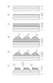
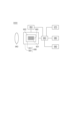
図1(a)は、光学装置930の一例の断面模式図を示す。光学装置930は基体10と、レンズアレイ200とを備える。レンズアレイ200は基体10の上にて複数のレンズ201、202、203が配列されてなる。複数のレンズ201、202、203の各々は、レンズの屈折面としての凸面または凹面を成す曲面(以下、レンズ曲面と称する)を有する。図1(a)では、レンズ曲面を、複数のレンズ201、202、203が矢印で指す点線で示している。本例では、レンズ201、202、203はそれぞれ上凸の平凸レンズであるから、レンズ201、202、203のレンズ曲面は、基体10の側とは反対側の凸面である。レンズ曲面は、少なくとも、珪素(Si)および窒素(N)を含む層である窒化シリコン層21と、珪素(Si)および窒素を含む層(N)である窒化シリコン層22と、で構成されている。窒化シリコン層21と窒化シリコン層22との間に窒化シリコン層21および窒化シリコン層22とは組成が異なる中間層23が設けられている。窒化シリコン層21が窒化シリコン層22と基体10との間に位置する。ここで、比較対象となる2つの層の「組成」が異なることは、2つの層の構成元素の少なくとも1つの元素の有無が異なる、つまり、2つの層の全構成元素が完全一致しないことを包含する。また、比較対象となる2つの層の「組成」が異なることは、2つの層の全構成元素が完全一致する場合、または、2つの層の全構成元素が完全一致しない場合であって、少なくとも1つの元素の濃度が異なることを包含する。
FIG. 1(a) shows a schematic cross-sectional view of an example of the
珪素(Si)および窒素(N)を含む層である窒化シリコン層21、22はその可視光に対する透過率、純粋な酸化シリコンや典型的な透明樹脂よりも高い屈折率を有する点でレンズ201、202、203の材料として適切である。レンズ201、202、203のパワーを高めるためにはレンズ201、202、203の高さを高くすることが有効である。その場合に、レンズ201、202、203を厚い単層の窒化シリコン層で構成すると、厚い単層の窒化シリコン層の内部応力が大きくなる。図1(a)には窒化シリコン層21の厚さTaと窒化シリコン層22の厚さTbとを示している。仮に中間層23がない場合、窒化シリコン層21と窒化シリコン層22とが連続することになり、厚さTa+Tbの厚い単層の窒化シリコン層でレンズアレイ200が構成されることになる。窒化シリコン層の厚さが大きければ大きいほど、窒化シリコン層の内部応力が大きくなる。窒化シリコン層の内部応力が大きくなると、レンズアレイ200に生じる歪みによって、レンズアレイ200の光学特性が低下する。これに対して、窒化シリコン層21と窒化シリコン層22との間に中間層23を設けることで、窒化シリコン層21と窒化シリコン層22とを不連続にし、内部応力の増大を抑制している。つまり、中間層23は窒化シリコン層21と窒化シリコン層22との間の応力緩和層として機能しうる。窒化シリコン層21と窒化シリコン層22とが組成的に不連続であればよいので、中間層23の組成がおよび窒化シリコン層21と窒化シリコン層22の組成と異なっていればよい。
The
中間層23の厚さTcは窒化シリコン層21の厚さTaよりも小さいこと(Tc<Ta)が好ましい。中間層23の厚さTcは窒化シリコン層22の厚さTbよりも小さいこと(Tc<Tb)が好ましい。中間層23の厚さTcを窒化シリコン層21の厚さTaや窒化シリコン層22の厚さTbよりも小さくすることで、中間層23による光学的影響を、窒化シリコン層21、22による光学的影響よりも少なくすることができる。仮に中間層23の厚さTcを、窒化シリコン層21の厚さTa以上、かつ、窒化シリコン層22の厚さTb以上にすると、中間層23での光の屈折が窒化シリコン層21での光の屈折と窒化シリコン層22での光の屈折に対して無視できないほど大きくなる。そのため、球面収差、コマ収差、非点収差などの収差が生じて、レンズ201、202、203の光学特性が低下する。中間層23の厚さTcを、窒化シリコン層21の厚さTa未満、かつ、窒化シリコン層22の厚さTb未満にすることで、光学特性を向上できる。例えば、中間層23内での光路長を、窒化シリコン層21、22内での光路長よりも短くすることができるため、中間層23内での屈折の影響は窒化シリコン層21、22内での屈折の影響よりも小さくできる。なお、厳密には中間層23はレンズ曲面を構成しうるが、中間層23がレンズ曲面を構成することは本質的でない。なぜなら、本実施形態の思想として、レンズにおける主たる屈折体は窒化シリコン層21と窒化シリコン層22であって、中間層23がレンズにおける屈折体として実質的な機能を有しないことが理想的であるからである。
The thickness Tc of the
中間層23の厚さTcは窒化シリコン層21の厚さTaの1/10以下でありうる(Tc≦Ta/10)。中間層23の厚さTcは窒化シリコン層21の厚さTbの1/10以下でありうる(Tc≦Tb/10)。中間層23の厚さTcは窒化シリコン層21の厚さTaと窒化シリコン層22の厚さTbの和の1/10以下でありうる(Tc≦(Ta+Tb)/10)。中間層23の厚さTcは窒化シリコン層21の厚さTaと窒化シリコン層22の厚さTbの和の1/100以下でありうる(Tc≦(Ta+Tb)/100)。窒化シリコン層21の厚さTaと窒化シリコン層22の厚さTbの和は例えば800nm以上であり(Ta+Tb≧800nm)、例えば1000nm以上である(Ta+Tb≧1000nm)。窒化シリコン層21の厚さTaは、例えば100nm以上であり、例えば300nm以上であり、例えば500nm以上であり、例えば1000nm以下であり、例えば800nm以下である。窒化シリコン層22の厚さTbは、例えば100nm以上であり、例えば300nm以上であり、例えば1000nm以下であり、例えば800nm以下であり、例えば500nm以下である。窒化シリコン層22の厚さTbが窒化シリコン層21の厚さTaよりも小さくなりうる(Ta>Tb)。中間層23の厚さTcは20nm未満でありうる(Tc<20nm)。中間層23の厚さTcが20nm未満であれば、可視光に対する中間層23の光学的な影響をほとんど無視できるようになる。中間層23の厚さTcは、レンズ201、202、203に入射する光の波長λ、中間層23の屈折率Ncに対して、Nc×Tc<λ/10であることが好ましい。Nc×Tcは中間層23の光学膜厚である。化学量論的組成の窒化シリコン(Si3N4)の屈折率を2.0、化学量論的組成の窒化シリコン(SiO2)の屈折率を1.5とすると、窒化シリコン層が酸化されて形成された中間層23の屈折率は1.5~2.0である。ここで、入射光が可視光である場合を考える。なお、可視光の波長は400~800nmであるものとする。厚さTcが20nm未満であれば、中間層23の屈折率が2.0以下でありさえすれば、入射光の波長が400nm以上の場合に、Nc×Tc<λ/10を満たす。中間層23の厚さTcは5nm以下でありうる(Tc≦5nm)。屈折率Ncが8.0である中間層23を仮定すると、入射光の波長が400nm以上の場合に、厚さTcが5nm未満であれば、Nc×Tc<λ/10を満たす。よって、仮に中間層23が単結晶シリコン(屈折率は5.6~3.5)のような高屈折率材料であったとしても、波長が400nm以上である入射光に対して、中間層23は屈折による光学特性への影響をほとんど生じない。なお、仮に中間層23が光を吸収する特性があったとしても、厚さTcが20nm未満であれば、光の吸収による損失は無視できるし、厚さTcが5nm未満であれば、なおさらである。中間層23は少なくとも単原子層よりも厚く、中間層23の厚さTcは1Å以上でありうる(Tc≧1Å)。中間層23の厚さTcは1nm以上でありうる(Tc≧1nm)。
The thickness Tc of the
窒化シリコン層21と中間層23との間の距離は中間層23の厚さよりも小さくなりうる。本例において窒化シリコン層21と中間層23は互いに接しており、窒化シリコン層21と中間層23との間の距離はゼロである。窒化シリコン層22と中間層23との間の距離は中間層23の厚さよりも小さくなりうる。本例において窒化シリコン層22と中間層23は互いに接しており、窒化シリコン層22と中間層23との間の距離はゼロである。
The distance between
光学装置930は、レンズの曲面に沿って設けられた反射防止層24を備えうる。本例の反射防止層24は珪素と窒素と酸素を含む層(酸窒化シリコン層)である。光学装置930は、レンズアレイ200に対して基体10の側とは反対側に設けられた平坦化層25を備えうる。本例の平坦化層は珪素と酸素を含む層(酸化シリコン層)であるが、樹脂を含む層(樹脂層)であってもよい。平坦化層25の下面はレンズ曲面に沿った形状を有し、平坦化層25の上面は平坦化層25の下面よりも平坦であり、平坦化層25の上面はレンズ曲面よりも平坦である。本例の反射防止層24は平坦化層25とレンズアレイ200との間に配されており、平坦化層25からレンズアレイ200へ入射する光の反射を抑制する。反射防止層24を省略して、平坦化層25がレンズアレイ200に接するようにすることもできる。平坦化層25を省略して、空気等の外部媒質からレンズアレイ200へ入射するように構成することもでき、その場合にも反射防止層24を設けることは有用である。反射防止層24の屈折率は、レンズ曲面を構成する窒化シリコン層21、22の屈折率と、レンズアレイ200に対して、光が入射する側の媒質(本例では平坦化層25)の屈折率との間の屈折率を有することが好ましい。反射防止層24と平坦化層25をともに省略し、外部媒質からレンズアレイ200へ光が直接的に入射するように構成することもできる。
The
反射防止層24の厚さTdは窒化シリコン層21の厚さTaよりも小さくてよい(Td<Ta)。反射防止層24の厚さTdは窒化シリコン層22の厚さTbよりも小さくてよい(Td<Ta)。反射防止層24の厚さTdが中間層23の厚さTcよりも大きいことが好ましい(Tc<Td)。また、このように中間層23の厚さTcを他の層よりも小さくすることで、中間層23以外の層が生じる光学的な作用に比べて、中間層23が生じうる光学的な作用を小さくし、中間層23の光学的な影響を小さくすることができる。反射防止層24の厚さTdは、例えば100nm以下であってよく、20nm以上であってよく、50nm以上であってよい。窒化シリコン層21と反射防止層24との間の距離は窒化シリコン層22の厚さTbよりも小さくなりうる。窒化シリコン層21と反射防止層24との間の距離は反射防止層24の厚さTdよりも小さくなりうる。本例において窒化シリコン層21と反射防止層24は互いに接しており、窒化シリコン層21と反射防止層24との間の距離はゼロである。窒化シリコン層22と反射防止層24との間の距離は反射防止層24の厚さTdよりも小さくなりうる。本例において窒化シリコン層22と反射防止層24は互いに接しており、窒化シリコン層22と反射防止層24との間の距離はゼロである。
The thickness Td of the
反射防止層24がレンズアレイ200のレンズ曲面に沿った凹凸を有する。一方、反射防止層24が凹凸を有するのと対照的に、中間層23は基体10の主面に沿って平坦であり、反射防止層24の凹凸よりも、中間層23の基体10からの高低差が小さい。反射防止層24の凹凸は、窒化シリコン層21、22が有する、窒化シリコン層21、22の厚さTa、Tb以下の凹凸に起因するものである。中間層23は中間層23の基体10からの高低差が窒化シリコン層21の厚さTaよりも小さくなりうる。中間層23の基体10から高低差が窒化シリコン層22の厚さTcよりも小さくなりうる。
The
平坦化層25や反射防止層24は、複数のレンズ201、202、203の間に位置する部分(中間部分)部分を有する。この中間部分と基体10との間に、レンズ201、202、203を構成する層が延在部分204、205、206、207を有するように位置している。本例では、延在部分204、205、206、207は窒化シリコン層21によって構成されている。つまり、中間部分と、基体10との間に窒化シリコン層21が延在している。延在部分204、205、206、207を中間層23や窒化シリコン層22で構成することもできる。しかしながら、本例のように、窒化シリコン層22が複数のレンズ201、202、203の間で不連続であることが好ましい。
The
また、本例のように、中間層23が複数のレンズ201、202、203の間で不連続であることが好ましい。窒化シリコン層22や中間層23が複数のレンズ201、202、203の間で不連続となるような位置に、窒化シリコン層22や中間層23を配置することは、複数のレンズ201、202、203の光学特性を向上するうえで有利である。延在部分204、205、206、207における窒化シリコン層21の厚さTeはレンズ201、202、203における窒化シリコン層21の厚さTaよりも小さくなりうる(Te<Ta)。例えば、厚さTeは厚さTaの1/2以下であってよく、厚さTeは厚さTaの1/3以下であってよく、厚さTeは厚さTaの1/4以上であってよい。延在部分204、205、206、207における窒化シリコン層21の厚さTeは窒化シリコン層22の厚さTbよりも小さくなりうる(Te<Tb)。例えば、厚さTeは厚さTbの1/2以下であってよく、厚さTeは厚さTbの1/4以上であってよい。厚さTeは厚さTdよりも大きくてよい(Td<Te)。厚さTeは例えば100nm以上であり、例えば500nm以下であり、例えば300nm以下である。
Moreover, it is preferable that the
図1(b)には、窒化シリコン層21、22と中間層23と反射防止層24と平坦化層25を含む部分における珪素(Si)と窒素(N)と酸素(O)のそれぞれの濃度の分布を示している。ここで、特に明記しない場合に濃度の単位はatom%(原子%)であり、atom%で表される濃度を相対濃度と称し、atom/cm3で表される濃度を絶対濃度と称する。相対濃度の分母は軽元素を除く元素の原子の個数である。
FIG. 1B shows the respective concentrations of silicon (Si), nitrogen (N) and oxygen (O) in the portion including the silicon nitride layers 21 and 22, the
図1(b)に示した濃度分布を説明するため、各層21、22、23、24、25について、各層の符号をQとして、珪素濃度を“Si[Q]”と表し、窒素濃度を“N[Q]”、酸素濃度を“O[Q]”とする。例えば窒化シリコン層21の窒素濃度は、Q=21なのでN[21]で表され、中間層23の酸素濃度はQ=23なのでO[23]で表される。図1(b)から理解されるように、珪素濃度の関係は、例えばSi[25]<Si[24]<Si[23]<Si[21]=Si[22]を満たしうる。窒素濃度の関係は、例えばN[25]<N[24]<N[23]<N[21]=N[22]を満たしうる。酸素濃度の関係は、例えばO[21]=O[22]<O[23]<O[24]<O[25]を満たしうる。各層21、22、23、24、25の組成がこの関係の少なくとも一部を満足することは、複数のレンズの光学特性を向上するうえで有利である。
In order to explain the concentration distribution shown in FIG. 1(b), for each of the
中間層23は酸素を含みうる。中間層23における酸素濃度が、窒化シリコン層21における酸素濃度よりも高い。また、中間層23における酸素濃度が、窒化シリコン層22における酸素濃度よりも高い。本例の中間層23は窒化シリコン層の表面が自然酸化することによって形成されている。そのため、中間層23は珪素、窒素および酸素を含みうる。中間層23が窒化シリコンの自然酸化によって形成される場合、中間層23の珪素濃度(atom%)は窒化シリコン層21、22の珪素濃度よりも低くなりうる。中間層23の酸素の絶対濃度は、窒化シリコン層21、22の酸素の絶対濃度よりも高い。また、中間層23の窒素濃度(atom%)は窒化シリコン層21、22の窒素濃度よりも低くなりうる。これは、元から存在する珪素と窒素に、自然酸化によって酸素が追加されたことによって相対的に珪素および窒素が減少するからである。そのため、中間層23の窒素の絶対濃度は、窒化シリコン層21、22の窒素の絶対濃度と等しくてもよく、中間層23の珪素の絶対濃度は、窒化シリコン層21、22の珪素の絶対濃度と等しくてもよい。中間層23の組成の他の例として中間層23は炭素を含みうる。炭素を含む中間層は窒化シリコン層の表面に有機物が吸着することによって形成されうる。その場合、中間層23は珪素、窒素および炭素を含みうる。自然酸化および有機物の吸着の両方が生じてもよく、その場合、中間層23は珪素、窒素、酸素および炭素を含みうる。中間層23が任意の元素を含むように、成膜装置を用いて人工的に中間層23を形成してもよい。自然酸化や吸着によって形成される中間層23の厚さTcは5nm以下でありうる(Tc≦5nm)。
窒化シリコン層21、22が化学量論的組成を有する窒化シリコンからなる場合にはSi3N4の組成となるが、窒化シリコン層21、22は非化学量論的組成を有していてもよい。窒化シリコン層21、22は、珪素および窒素よりも少ない、軽元素(水素(H)とヘリウム(He))以外の元素を含んでいてもよい。珪素および窒素の少なくとも一方よりも多い、軽元素以外の元素を含んでいてもよい。窒化シリコン層21、22が含みうる、軽元素以外の元素としては、炭素(C)、酸素(O)、弗素(F)、塩素(Cl)、アルゴン(Ar)が例示される。窒化シリコン層21、22は珪素および窒素の少なくとも一方よりも多い軽元素(水素(H)とヘリウム(He))を含みうる。窒化シリコン層21、22が含む軽元素は珪素および窒素よりも少なくてもよい。 When the silicon nitride layers 21 and 22 are made of silicon nitride having a stoichiometric composition, they have a composition of Si 3 N 4 . good. The silicon nitride layers 21 and 22 may contain elements other than light elements (hydrogen (H) and helium (He)) less than silicon and nitrogen. Elements other than light elements may be contained in a larger amount than at least one of silicon and nitrogen. Examples of elements other than light elements that the silicon nitride layers 21 and 22 may contain include carbon (C), oxygen (O), fluorine (F), chlorine (Cl), and argon (Ar). The silicon nitride layers 21, 22 may contain more light elements (hydrogen (H) and helium (He)) than at least one of silicon and nitrogen. Light elements contained in the silicon nitride layers 21 and 22 may be less than silicon and nitrogen.
反射防止層24の酸素濃度が中間層23の酸素濃度よりも高くてもよい。中間層23に含まれる酸素が多いと、中間層23の屈折率と窒化シリコン層21、22の屈折率の差が大きくなり、窒化シリコン層21と窒化シリコン層22との間での光の反射が増大しうる。中間層23の酸素濃度を酸窒化シリコン層である反射防止層24の酸素濃度よりも低くすることで、窒化シリコン層21と窒化シリコン層22との間での光の反射を低減できる。
The oxygen concentration of the
図1(b)に記載した濃度分布における各元素の濃度の一例を説明する。下記に示した各層の元素濃度の範囲から、珪素濃度と窒素濃度と酸素濃度の和が100atom%を超えないように適宜調整することができる。窒化シリコン層21および窒化シリコン層22における珪素濃度は、例えば50atom%以上であり、例えば80atom%以下である。中間層23における珪素濃度は、例えば1atom%以上であり、例えば10atom%以上であり、例えば30atom%以上であり、例えば80atom%以下である。反射防止層24および平坦化層25における珪素濃度は、例えば20atom%以上であり、例えば60atom%以下である。窒化シリコン層21および窒化シリコン層22における窒素濃度は、例えば20atom%以上であり、例えば50atom%以下である。中間層23における窒素濃度は、例えば1atom%以上であり、例えば10atom%以上であり、例えば20atom%以上であり、例えば40atom%以下である。反射防止層24における窒素濃度は、例えば10atom%以上であり、例えば40atom%以下である。平坦化層25における窒素濃度は、例えば10atom%未満あり、例えば1atom%未満であり、例えば0atom%である。平坦化層25における酸素濃度は、例えば50atom%以上であり、例えば80atom%以下である。反射防止層24における酸素濃度は、例えば10atom%以上であり、例えば40atom%以下である。中間層23における酸素濃度は、例えば1atom%以上であり、例えば10atom%以上であり、例えば60atom%以下であり、例えば20atom%以下である。窒化シリコン層21および窒化シリコン層22における酸素濃度は、例えば10atom%未満あり、例えば1atom%未満であり、例えば0atom%である。
An example of the concentration of each element in the concentration distribution shown in FIG. 1(b) will be described. From the range of the element concentration of each layer shown below, the sum of the silicon concentration, the nitrogen concentration and the oxygen concentration can be appropriately adjusted so as not to exceed 100 atom %. The silicon concentration in the
図2(a)~(f)は、図1(a)で示した光学装置930の製造方法を工程順に示す断面模式図である。
2(a) to 2(f) are schematic cross-sectional views showing the steps of a method for manufacturing the
図2(a)に示す工程aでは、基体10の上に窒化シリコン膜210を形成する。窒化シリコン膜210が後に窒化シリコン層21になる。
In step a shown in FIG. 2A, a
図2(b)に示す工程bでは、窒化シリコン膜210の上に、窒化シリコン膜210とは組成が異なる異組成膜230を形成する。異組成膜230が後に中間層23になる。異組成膜230の厚さは窒化シリコン膜210の厚さよりも小さくすることができる。異組成膜230の厚さは窒化シリコン膜210の厚さの1/10以下であることが好ましい。異組成膜230の厚さは窒化シリコン膜210の厚さの1/100以下であることがより好ましい。異組成膜230は、窒化シリコン膜210の成膜装置のチャンバー内に空気等の酸素含ガスを導入することで、窒化シリコン膜210をチャンバー内で自然酸化することで形成することができる。異組成膜230は、窒化シリコン膜210の成膜装置のチャンバーから取り出して、基体10の上に成膜された窒化シリコン膜210を空気等の酸素含ガスに晒すことで、窒化シリコン膜210を自然酸化することで形成することもできる。異組成膜230は、窒化シリコン膜210の成膜装置のチャンバー内の雰囲気中の有機物を窒化シリコン膜210に吸着させることで形成することもできる。異組成膜230は、窒化シリコン膜210の成膜装置、あるいは、窒化シリコン膜210の成膜装置とは別の成膜装置を用いて、窒化シリコン膜210の成膜条件とは異なる成膜条件で成膜することもできる。異組成膜230をスパッタ法、蒸着法、熱CVD(Chemical Vapor Deposition)法、プラズマCVD法、ALD(Atomic Layer Deposition)法のいずれかを用いて形成することができる。
In step b shown in FIG. 2B, a
図2(c)に示す工程cでは、異組成膜230の上に窒化シリコン膜220を形成する。窒化シリコン膜220が後に窒化シリコン層22になる。窒化シリコン膜220の厚さは異組成膜230の厚さよりも大きくすることができる。窒化シリコン膜220の厚さは異組成膜230の厚さの10倍以上であることが好ましい。窒化シリコン膜220の厚さは異組成膜230の厚さの100倍以上であることがより好ましい。
In step c shown in FIG. 2C, a
窒化シリコン膜210、220は、スパッタ法、蒸着法、熱CVD(Chemical Vapor Deposition)法、プラズマCVD法、ALD(Atomic Layer Deposition)法のいずれかを用いて形成することができる。レンズ201、202、203の窒化シリコン層21、22として良好な屈折率、透過率を実現するためには、窒化シリコン膜210、220をCVD法で形成することが好ましい。窒化シリコン膜210、220の成膜時の基体10の熱膨張によって生じうる応力を考慮すると、窒化シリコン膜210、220を熱CVD法よりもプラズマCVD法で形成することが好ましい。より厚い窒化シリコン膜210、220は、レンズ201、202、203の高さを高くする(厚くする)上で有利であり、また、レンズ201、202、203内に生じうる異種材料の界面の数を減らすうえでも有利である。そのため、窒化シリコン膜210、220の厚さは、例えば100nm以上とすることができ、例えば300nm以上とすることができ、例えば500nm以上とすることができる。一方、窒化シリコン膜210、220が厚ければ厚いほど、窒化シリコン膜210、220に生じる応力が増大する。そこで、窒化シリコン膜210、220の厚さは、1000nm以下とすることができ、例えば800nm以下とすることができる。
The
図2(d)に示す工程dでは、窒化シリコン膜220の上に被転写部材241、242、243を形成する。被転写部材241、242、243は後で形成されるレンズ201、202、203のレンズ曲面に対応した略半球状の曲面を有する。被転写部材241、242、243は例えば感光性樹脂からなる。曲面を有する被転写部材241、242、243は、感光性樹脂膜(フォトレジスト膜)をレチクル(フォトマスク)を用いて露光し、現像によってパターニングして形成された感光性樹脂パターンをリフローして形成することができる。あるいは、曲面を有する被転写部材241、242、243は、感光性樹脂膜を、ハーフトーンレチクルの透過率分布(階調)に応じて露光量分布が生じるように露光し、これを現像することで露光量分布に応じた膜厚分布を有するように形成されてもよい。いずれにしても、被転写部材241、242、243となる感光性樹脂を露光機によって露光する際には、下地である基体10に形成したパターンと、レチクルとの位置合わせ(アライメント)が行われる。このアライメントの際に、被転写部材241、242、243の下地となる窒化シリコン膜の内部応力が大きいと、アライメト誤差が大きくなる。しかし、異組成膜230を介して窒化シリコン膜210と窒化シリコン膜220とを重ねることで、連続した窒化シリコン膜の厚さの増大を抑制し、被転写部材241、242、243の下地となる窒化シリコン膜の応力を低減することができる。その結果、重ね合わせ精度の低下を抑制できたり、アライメント精度が向上したりする。
In step d shown in FIG. 2D, transferred
図2(e)に示す工程eでは、被転写部材241、242、243を用いて窒化シリコン膜220をエッチングする。この時、被転写部材241、242、243と窒化シリコン膜220のエッチング選択比が小さくなる条件(選択比は例えば1~10)でエッチングを行うと、被転写部材241、242、243の曲面形状が窒化シリコン膜220に転写される。工程eでは異組成膜230が露出しうる。この段階では、窒化シリコン膜220の上には被転写部材241、242、243の一部が残存しうる。
In step e shown in FIG. 2E, the
図2(f)に示す工程fでは、工程eに引き続き、窒化シリコン膜220と異組成膜230と窒化シリコン膜210のエッチングを行う。これにより、窒化シリコン膜220と異組成膜230と窒化シリコン膜210に被転写部材241、242、243の形状を転写し、レンズ201、202、203を形成する。工程fでは、工程eとエッチング条件を異ならせてもよいが、工程eと同じエッチング条件でエッチングを進めることができる。異組成膜230の厚さが窒化シリコン膜210、220の厚さより小さければ、異組成膜230のエッチングレートが窒化シリコン膜210、220のエッチングレートよりも低くても、異組成膜230を設けることによるエッチング時のスループットの低下は小さい。
In step f shown in FIG. 2(f), the
工程aから工程cにおいて、先に成膜される窒化シリコン膜210と、後に成膜される窒化シリコン膜220とで成膜方法を異ならせる必要がない。しかし、窒化シリコン膜210、220の一方が窒化シリコン膜210、220の他方よりも応力分布が大きくなるように、窒化シリコン膜210、220を成膜してもよい。その場合、先に成膜される窒化シリコン膜210の応力分布が、後に成膜される窒化シリコン膜220の応力分布よりも大きいこと(条件1とする)が好ましい。条件1の方が、先に成膜される窒化シリコン膜210の応力分布が、後に成膜される窒化シリコン膜220の応力分布よりも小さい場合(条件2とする)よりも、異組成膜230を形成することにより応力緩和効果が高い。この応力緩和効果の大小は、パターニング後のレンズ201、202、203と、下地である基体10に形成したパターンとの重ね合わせ精度によって評価した結果である。発明者らの検討では、条件1では条件2に対して20%の重ね合わせ精度の改善を確認した。
In steps a to c, there is no need to use different deposition methods for the
図3(a)は図1(a)に示した例の変形例である。光学装置930は、複数のレンズ201、202、203の間に設けられた遮光壁721、722を備える。遮光壁721、722はタングステン等の金属からなる。遮光壁721、722を設けることで、レンズ201、202、203に入射する光のクロストークを抑制できる。本例の遮光壁721、722は反射防止層24を貫通して窒化シリコン層21に接するが、遮光壁721、722が、遮光壁721、722と窒化シリコン層21との間の反射防止層24を介して、窒化シリコン層21から離間してもよい。
FIG. 3(a) is a modification of the example shown in FIG. 1(a). The
図3(a)の変形例における光学装置930は、レンズアレイ200と基体10との間に設けられた低屈折率層11を備えうる。低屈折率層11は窒化シリコン層21、22よりも低い屈折率を有する。本例の低屈折率層11は珪素と酸素を含む層(酸化シリコン層)である。光学装置930は、レンズアレイ200と基体10との間に設けられた反射防止層12を備えうる。反射防止層12は窒化シリコン層21、22よりも低い屈折率を有し、低屈折率層11と窒化シリコン層21との間の屈折率を有しうる。本例の反射防止層12は珪素と窒素と酸素を含む層(酸窒化シリコン層)である。反射防止層12の組成は反射防止層24と同様であってよい。反射防止層12の厚さTfは、反射防止層12の厚さTdと同様に、窒化シリコン層21の厚さTaよりも小さくてよく、窒化シリコン層22の厚さTbよりも小さくてよく、中間層23の厚さTcよりも大きくてよい。反射防止層12の厚さTfは、例えば100nm以下であってよく、20nm以上であってよく、50nm以上であってよい。
The
図1(a)あるいは図3(a)に関して、各層の厚さの関係は、例えばTc<10nm<Td=Tf<100nm<Te<Tb<Ta<1000nm<Ta+Tbでありうる。各層の厚さがこの関係の少なくとも一部を満足することは、複数のレンズの光学特性を向上するうえで有利である。 With respect to FIG. 1(a) or FIG. 3(a), the thickness relationship of each layer can be, for example, Tc<10 nm<Td=Tf<100 nm<Te<Tb<Ta<1000 nm<Ta+Tb. Satisfying at least part of this relationship for the thickness of each layer is advantageous for improving the optical properties of a plurality of lenses.
図3(b)は図1(a)に示した例の変形例である。光学装置930が備える複数のレンズ201、202、203は両凸レンズであり。レンズ曲面のうちの基体10とは反対側の凸面が窒化シリコン層21と窒化シリコン層22とで構成され、窒化シリコン層21と窒化シリコン層22との間に中間層23が位置する点は図1(a)の例と共通である。図3(b)の例では、レンズ曲面のうちの基体10の側の凸面が窒化シリコン層27で構成され、窒化シリコン層27と窒化シリコン層21の間に中間層28が位置している。窒化シリコン層27の組成や厚さは窒化シリコン層21と同様であってよく、中間層28の組成や厚さは中間層23と同様であってよい。レンズ201、202、203との間には凹面を有する低屈折率層11が位置しており、低屈折率層11の凹面に沿って反射防止層12が位置している。このような構造は、凹面を有する低屈折率層11上に、反射防止層12になる酸窒化シリコン膜と、窒化シリコン層27になる窒化シリコン膜を成膜し、窒化シリコン層27となる窒化シリコン膜の上に中間層28となる異組成膜を形成する。中間層28となる異組成膜の上に窒化シリコン層27となる窒化シリコン膜を形成し、窒化シリコン層27となる窒化シリコン膜をCMP法などにより平坦化する。平坦化された窒化シリコン層27となる窒化シリコン膜の上に中間層23となる異組成膜と窒化シリコン層22となる窒化シリコン膜を形成する。この後は、図2で示した方法と同様にして、基体10とは反対側の凸面を有するように窒化シリコン層22となる窒化シリコン膜、中間層23となる異組成膜、窒化シリコン層21なる窒化シリコン膜、中間層28となる異組成膜、を順次エッチングする。
FIG. 3(b) is a modification of the example shown in FIG. 1(a). A plurality of
図1(a)、図3(a)、図3(c)では、レンズ曲面を主に2層の窒化シリコン層21、22で構成する例を示したが、3層以上の窒化シリコン層でレンズ曲面を構成してもよい。そして、それぞれの窒化シリコン層の間に、窒化シリコン層とは組成が異なり、窒化シリコン層よりも薄い中間層を配置すればよい。レンズ曲面を構成する窒化シリコン層の層数は中間層の層数よりも多いことが好ましい。レンズ曲面を構成する窒化シリコン層の層数は、中間層の層数の3/2倍よりも大きくてよく、中間層の層数の3倍よりも小さくてよい。 1(a), 3(a), and 3(c) show an example in which the lens curved surface is mainly composed of two silicon nitride layers 21 and 22, but three or more silicon nitride layers may be used. A lens curved surface may be configured. Then, an intermediate layer having a composition different from that of the silicon nitride layer and being thinner than the silicon nitride layer may be arranged between the respective silicon nitride layers. The number of silicon nitride layers forming the curved surface of the lens is preferably greater than the number of intermediate layers. The number of silicon nitride layers forming the curved surface of the lens may be larger than 3/2 times the number of intermediate layers and may be smaller than three times the number of intermediate layers.
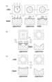
図4(a)は、図3(b)に示したレンズ下面の非球面をウエットエッチッチングで形成するプロセスフローを示す概略図である。曲率半径を小さくすると一般に収差が発生しやすくなる。そこで、基体10に近い面を非球面とすることで、両凸層内レンズで発生する収差、特に球面収差、を補正することも可能である。併せて低屈折率材料を使うことで所望の焦点距離を得るためには曲率半径を小さくする必要がなくなり、ここでも収差を軽減することが可能となる。低屈折率材料として、例えば東京応化製のLALシリーズの屈折率は1.2である。低屈折率材料を凹形状に形成し、その後、高屈折率、例えば屈折率は2程度の材質、例えば窒化シリコン膜を成膜することで、下面が凸レンズとして働く。窒化シリコン膜を、図3(b)に示すように、自然酸化膜からなる中間層28、23を介して、3回にわけて成膜する。この時、超低屈折率材料の凹形状の周辺部を非球面にして球面収差を低減するには、周辺部の曲率を大きくすることが好ましい。そのためには、スリットSを有するマスク材Mを用いて、レジストR1がマスク材Mの孔Hを塞いだ状態で、低屈折率材料に等方的なウエットエッチングエッチングを施して周辺部の凹部を形成する。また、孔Hを有するマスク材Mを用いて、レジストR2がマスク材MのスリットSを塞いだ状態で、低屈折率材料に等方的なウエットエッチングエッチングを施して中央部の凹部を形成する。図4(b)は、低屈折率材料の凹形状の別の形成方法を示す図であり、層内レンズ下面の非球面を、階調マスク露光でパターニングされたレジストR3をエッチバックで低屈折率材料に転写して形成するプロセスフローを示す概略図である。階調マスク露光とエッチバックによっても非球面の凹形状を形成することが可能となる。
FIG. 4(a) is a schematic diagram showing a process flow for forming the aspheric surface on the lower surface of the lens shown in FIG. 3(b) by wet etching. Aberrations generally tend to occur when the radius of curvature is reduced. Therefore, by making the surface closer to the base 10 an aspherical surface, it is also possible to correct aberrations, particularly spherical aberration, that occur in the biconvex in-layer lens. In addition, by using a low refractive index material, it becomes unnecessary to reduce the radius of curvature to obtain a desired focal length, and aberrations can be reduced here as well. As a low refractive index material, for example, the LAL series manufactured by Tokyo Ohka has a refractive index of 1.2. A low refractive index material is formed in a concave shape, and then a material having a high refractive index, for example, a refractive index of about 2, such as a silicon nitride film, is deposited, so that the lower surface functions as a convex lens. As shown in FIG. 3B, a silicon nitride film is formed in three steps through
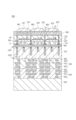
図5は、光学装置930が表面照射型の撮像装置である形態を示している。図1(a)や図3(a)で示した基体10は、半導体層100、配線構造440、導光部451、452、453、導光部451、452、453を連結する連結部450を含んでいる。半導体層100には複数のフォトダイオード101、102、103、104、105、106が設けられている。フォトダイオード101、102、103、104、105、106の各々が光電変換部である。配線構造440はレンズアレイ200と半導体層100との間に位置する。
FIG. 5 shows an embodiment in which the
光学装置930は、平坦化層25の上に設けられ、赤色のカラーフィルタ861、緑色のカラーフィルタ862、青色のカラーフィルタ863を含む、カラーフィルタアレイを備える。光学装置930は、レンズアレイ200に対して基体10の側とは反対側に設けられた、別のレンズアレイ(マイクロレンズアレイ)を備える。マクロレンズアレイは、カラーフィルタアレイの上に平坦化層850を介して配列された、マイクロレンズ871、872、873を含む。すなわち、レンズアレイ200のレンズ201、202、203は層内レンズでありうる。
The
複数のレンズ201、202、203のうちの1つのレンズ201に、複数のフォトダイオード101、102、103、104、105、106のうちの2つ以上(本例では2つ)のフォトダイオード106、101が対応している。複数のレンズ201、202、203のうちの1つのレンズ202に、複数のフォトダイオード101、102、103、104、105、106のうちの2つ以上(本例では2つ)のフォトダイオード102、103が対応している。複数のレンズ201、202、203のうちの1つのレンズ203に、複数のフォトダイオード101、102、103、104、105、106のうちの2つ以上(本例では2つ)のフォトダイオード104、105が対応している。同様に、カラーフィルタ861とマイクロレンズ871にフォトダイオード106、101が対応する。カラーフィルタ862とマイクロレンズ872にフォトダイオード102、103が対応する。カラーフィルタ863とマイクロレンズ873にフォトダイオード104、105が対応する。このように、1つのレンズあるいはカラーフィルタで定義される画素が2つ以上のフォトダイオードを有している。このような構成により、焦点検出や測距、ダイナミックレンジの拡大などが可能となる。このように、1つのレンズで定義される画素が2つ以上のフォトダイオードを有している場合、2つ以上のフォトダイオードの各々で光電変換される光を分離できる。分離精度を向上するためには、フォトダイオードに対して極力1つのレンズに近い位置に焦点を結ぶことが好ましい。上述のように、窒化シリコン層21、22と中間層23を備えることで、レンズ201、202、203の応力の低減と光学特性の劣化抑制を実現しつつ、レンズ201、202、203の厚さを大きくして、そのパワーを高めることができる。
one
配線構造440は、配線層410、420と、層間絶縁膜430とを含む。配線構造440の配線層410、420は半導体層100に設けられた半導体素子に接続されている。半導体層100に設けられた半導体素子は電極層400を含み、例えば電極層400をゲート電極として有するトランジスタでありうる。電極層400はポリシリコン層でありうる。半導体層100に設けられた半導体素子には、フォトダイオードで生じた電荷を転送する転送トランジスタや、フォトダイオードで生じた電荷に基づく電気信号を生成する増幅トランジスタなどを含む画素回路を構成する。画素回路の半導体素子はSTI構造を有する素子分離部109によって分離されている。層間絶縁膜430には開口が設けられており、この開口内に導光部451、452、453が位置する。導光部451、452、453の屈折率は層間絶縁膜430の少なくとも一部の絶縁体層よりも高く、導光部451、452、453がコア、層間絶縁膜430の少なくとも一部の絶縁体層がクラッドとなるコア-クラッド型の導光構造が構成されている。クラッドとなる絶縁体層は例えば酸化シリコンからなり、導光部451、452、453は窒化シリコンや樹脂からなる。層間絶縁膜430を2種類の以上の絶縁体層の積層構造とすることができる。層間絶縁膜430の一方の絶縁体層と他方の絶縁体層との屈折率が異なる場合、異種の絶縁体層の界面で光の反射が生じて感度が低下しうる。層間絶縁膜430に開口を設けて異種の絶縁体層を部分的に除去し、当該開口に共通の材料を埋め込んで、導光部451、452、453を形成してもよい。例えば、炭化シリコン層と酸化シリコン層の積層構造からなる層間絶縁膜430に炭化シリコン層と酸化シリコン層を貫通する開口を設け、その開口の中に酸化シリコン層を埋め込んで、導光部451、452、453を形成してもよい。
The
レンズ201、202、203に入射した光を、レンズ201、202、203から至近距離に位置する導光部451、452、453へ光を入射させるためには、レンズ201、202、203のパワーを高める必要がある。ここでいう至近距離の目安は、例えばレンズ201、202、203から導光部451、452、453の入り口までの距離が、1μm以下の場合である。上述のように、窒化シリコン層21、22と中間層23を備えることで、レンズ201、202、203の応力の低減と光学特性の劣化抑制を実現しつつ、レンズ201、202、203の厚さを大きくして、そのパワーを高めることができる。
In order to cause the light incident on the
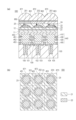
図5(b)は3×3画素分のレンズアレイ200を透過的に平面視したものを示している。図5(b)において、実線は窒化シリコン層22および中間層23の輪郭を示しており、点線はレンズ201、202、203の輪郭を示している。鎖線は導光部451、452、453の輪郭を示しており、2点鎖線はマイクロレンズ871、872、873の輪郭を示している。図5(b)では、窒化シリコン層21のうち、窒化シリコン層22および中間層23に重ならない部分のみをハッチングを付けて示しており、窒化シリコン層21のうち窒化シリコン層22と重なる部分については窒化シリコン層22のハッチングを付けている。図5(b)の例ではレンズ201、202、203の輪郭は円形であるが、多角形でもよく、角丸多角形でもよい。図5(b)の上下方向、左右方向および斜め方向において、レンズ201、202、203は離間している。レンズ201、202、203を隣り合うレンズから離間させることは、レンズ201、202、203の幅を小さくして、レンズ201、202、203曲率を大きくして、レンズ201、202、203のパワーを高めるうえで有用である。一方、マイクロレンズ871、872、873は上下方向、左右方向および斜め方向において、マイクロレンズ871、872、873は互いに境界をなしている。その結果、マイクロレンズ871、872、873の輪郭は四角形となっている。マイクロレンズ871、872、873が隣り合うレンズに隣接することは、マイクロレンズ871、872、873間での光の損失を低減するうえで有利である。図5(b)の例では導光部451、452、453の輪郭は、窒化シリコン層22および中間層23の輪郭に内包される。つまり、窒化シリコン層22および中間層23の幅が導光部451、452、453の幅よりも大きくなっている。このような関係にすることが、レンズ201、202、203へ入射した光を導光部451、452、453の内側に集光するうえで有利である。しかし、窒化シリコン層22および中間層23の輪郭が、導光部451、452、453の輪郭に内包されてもよい。つまり、窒化シリコン層22および中間層23の幅が導光部451、452、453の幅よりも小さくなってもよい。
FIG. 5B shows a transparent planar view of the
図5(a)に示した形態の変形例として、図5(a)のレンズ201、202、203の間に、図3(a)に示した遮光壁721、722を追加してもよい。
As a modification of the form shown in FIG. 5(a),
図6は、光学装置930が裏面照射型の撮像装置である形態を示している。図1(a)や図3(a)で示した基体10は、半導体層100、配線構造440、半導体基板600、配線構造540を含んでいる。配線構造440の配線層410、420は半導体層100に設けられた半導体素子に接続されている。配線構造540の配線層510、520は半導体基板600に設けられた半導体素子に接続されている。半導体基板600に設けられた半導体素子は電極層500を含み、例えば電極層500をゲート電極として有するトランジスタでありうる。電極層500はポリシリコン層でありうる。半導体基板600に設けられた半導体素子は、半導体層100に設けられた画素回路を駆動する駆動回路や、画素回路から出力された画素信号を処理する処理回路などの周辺回路を構成する。配線構造440とレンズアレイ200との間に半導体層100が位置する。半導体層100は裏面1001と表面1002とを有する。半導体層100には、裏面1001から連続する溝が設けられており、溝によって、分離部110、120、123、140、150、160、170が構成されている。分離部150、120、140は、フォトダイオード101とフォトダイオード106との間、フォトダイオード102とフォトダイオード103との間、フォトダイオード104とフォトダイオード105との間、に設けられている。分離部110、130は、フォトダイオード101とフォトダイオード102との間、フォトダイオード103とフォトダイオード104との間に設けられている。このように、分離部150、120、140は画素内の光学的および/または電気的な分離をなし、分離部110、130は画素間の光学的および/または電気的な分離をなす。分離部160、170も分離部110、130と同様に画素間の分離をなす。誘電体膜300は、酸化シリコン層や窒化シリコン層などのシリコン化合物層および/または金属酸化物層を含む多層膜でありうる。誘電体膜300に含まれる層は反射防止層や電荷固定層として機能する。誘電体膜300に含まれる層が分離部110、120、123、140、150、160、170を構成する。
FIG. 6 shows a form in which the
低屈折率層11と誘電体膜300との間には遮光部材710が設けられている。遮光部材710は分離部110、130、160、170に重なるように配置されうる。遮光部材710は分離部120、140、150に重ならないように配置されうる。遮光部材710の上には遮光壁720が設けられている。遮光壁720は、図3(a)の遮光壁721、722と同様に、レンズ201、202、203の間に配される。本例では、遮光壁720は、窒化シリコン層21(延在部分205、206)を貫通して、遮光部材710に接するように設けられている。そして、遮光壁720は層内レンズ201、202、203を囲むように配置されうる。
A
レンズ201、202、203に入射した光を、レンズ201、202、203から至近距離に位置する裏面1001の近傍で焦点を結ぶように集光するには、レンズ201、202、203のパワーを高める必要がある。ここでいう至近距離の目安は、例えばレンズ201、202、203から裏面1001までの距離が、2μm以下の場合である。上述のように窒化シリコン層21、22と中間層23を備えることで、レンズ201、202、203の応力の低減と光学特性の劣化抑制を実現しつつ、レンズ201、202、203の厚さを大きくして、そのパワーを高めることができる。また、図5の形態と同様に、201、202、203のパワーを高めることで、2つ以上のフォトダイオードに入射する光の分離精度を向上することもできる。
In order to focus the light incident on the
図5、図6では、窒化シリコン層21、22および中間層23で構成されたレンズアレイ200を1段だけ備える例を説明したが、窒化シリコン層21、22および中間層23で構成されたレンズアレイ200を複数段に重ねて設けてよい。レンズアレイ200を複数段設けることで、より焦点距離の短いオンチップ光学系を提供することができる。
5 and 6, an example in which only one stage of the
図7は、撮像装置としての光学装置930を備える機器9191の模式図である。機器9191は、光学装置930に加えて、光学系940、制御装置950、処理装置960、記憶装置970、表示装置980、および、機械装置990の少なくともいずれかを更に備える。制御装置950は光学装置930を制御する。処理装置960は光学装置930から出力された信号を処理する。記憶装置970は光学装置930で得られた情報を記憶する。表示装置980は光学装置930で得られた情報を表示する。機械装置990は光学装置930で得られた情報に基づいて動作する。機械装置990は光学装置930を機器9191の中で、あるいは機器9191ごと移動させる移動装置であってもよい。機器9191の中で光学装置930を移動させることで防振(イメージスタビライザー)機能を実現できる。
FIG. 7 is a schematic diagram of a
光学装置930は、電子デバイス910と実装部材920とを含みうるが、実装部材920は無くてもよい。電子デバイス910は、図1(a)に示した基体10に含まれる半導体層を有する半導体デバイスである。電子デバイス910は、画素が配列された画素エリア901と、周辺回路(不図示)が配列された周辺エリア902を含む。機器9191における画素エリア901に、本実施形態におけるレンズアレイ200を配置することができる。周辺回路には、上述の駆動回路やAD変換回路、デジタル信号処理回路や制御回路などが含まれる。光電変換エリア901と周辺回路エリア902は、同一の半導体層に配されてもよいが、本例では、互いに積層された別々の半導体層(半導体基板)に配されてもよい。
The
実装部材920は、セラミックパッケージやプラスチックパッケージ、プリント配線板、フレキシブルケーブル、半田、ワイヤボンディングなどを含む。光学系940は、例えばレンズやシャッター、フィルター、ミラーである。制御装置950、例えばASICなどの半導体デバイスである。処理装置960は、例えばAFE(アナログフロントエンド)あるいはDFE(デジタルフロントエンド)を構成する、例えばCPU(中央処理装置)やASIC(特定用途向け集積回路)などの半導体デバイスである。表示装置980は、例えばEL表示装置や液晶表示装置である。記憶装置970は、SRAMやDRAMなどの揮発性メモリ、あるいは、フラッシュメモリやハードディスクドライブなどの不揮発性メモリであり、例えば磁気デバイスや半導体デバイスである。機械装置MCHNはモーターやエンジン等の可動部あるいは推進部を有する。
The mounting
図7に示した機器9191は、撮影機能を有する情報端末(例えばスマートフォンやウエアラブル端末)やカメラ(例えばレンズ交換式カメラ、コンパクトカメラ、ビデオカメラ、監視カメラ)などの電子機器でありうる。カメラにおける機械装置990はズーミングや合焦、シャッター動作のために光学系940の部品を駆動することができる。レンズ交換式カメラとしてはレフレックス方式(一眼レフカメラ)よりもノンレフレックス方式(ミラーレスカメラ)に好適である。ノンレフレックス方式ではミラーがない分、イメージセンサセンサー(撮像装置)までのフランジバックが短くなり、バックフォーカスも短くなる。そのため、ノンレフレックス方式のカメラには、レフレックス方式のカメラよりパワーの大きいオンチップレンズアレイが必要となる。上述のように、本明細書に開示した技術は、そのような要求を満足する、光学特性に優れたオンチップレンズアレイを備えたセンサーを有するカメラを提供できる。
The
また、機器9191は、車両や船舶、飛行体、人工衛星などの輸送機器(移動体)でありうる。輸送機器における機械装置990は移動装置として用いられうる。輸送機器としての機器9191は、光学装置930を輸送するものや、撮影機能により運転(操縦)の補助および/または自動化を行うものに好適である。運転(操縦)の補助および/または自動化のための処理装置960は、光学装置930で得られた情報に基づいて移動装置としての機械装置990を操作するための処理を行うことができる。また、機器9191は、分析機器や、医療機器でありうる。
In addition, the
本実施形態による光学装置930は、その設計者、製造者、販売者、購入者および/または使用者に、高い価値を提供することができる。そのため、光学装置930を機器9191に搭載すれば、機器9191の価値も高めることができる。よって、機器9191の製造、販売を行う上で、本実施形態の光学装置930の機器9191への搭載を決定することは、機器9191の価値を高める上で有利である。
The
図5、6では、光学装置930として画像を生成する撮像装置を例示したが、光電変換部としてのフォトダイオードを有する光電変換装置としては、撮像装置の他に、測光装置、光検出装置、測距装置、焦点検出装置などであってもよい。また、レンズアレイを有する光学装置930は表示装置であってもよい。表示装置におけるレンズアレイは表示に用いられる光を集光することで、精細感や光利用効率などの面で、画質を向上することができる。かかる表示装置は有機EL素子などを有する自発光型の表示装置であってもよいし、透過型あるいは反射型の表示装置であってもよい。機器9191における光学系940は表示装置に対応付けられて、光学装置930が表示した映像を外部へ投影する。機器9191における処理装置960は表示装置へ入力する信号を処理する。
5 and 6 illustrate an imaging device that generates an image as the
以上、説明した実施形態は、本発明の思想を逸脱しない範囲において適宜変更が可能である。 The embodiments described above can be modified as appropriate without departing from the spirit of the present invention.
10 基体
201、202、202 レンズ
21 窒化シリコン層
22 窒化シリコン層
23 中間層
REFERENCE SIGNS
Claims (20)
前記基体の上に配列された複数のレンズと、
を備える光学装置であって、
複数のレンズの各々のレンズの凸面または凹面を成す曲面は、少なくとも、珪素および窒素を含む第1層と、珪素および窒素を含む第2層と、で定義されており、
前記第1層は前記第2層と前記基体との間に設けられており、
前記第1層と前記第2層との間に、前記第1層および前記第2層とは組成が異なる第3層が設けられており、
前記第3層の厚さは前記第1層の厚さおよび前記第2層の厚さよりも小さく、
前記第3層の厚さは前記第1層の厚さの1/10以下であり、
前記第3層の厚さは前記第2層の厚さの1/10以下であり、
前記第2層は前記複数のレンズの間で不連続である、
ことを特徴とする光学装置。 a substrate;
a plurality of lenses arranged on the base;
An optical device comprising
The convex or concave curved surface of each lens of the plurality of lenses is defined by at least a first layer containing silicon and nitrogen and a second layer containing silicon and nitrogen,
The first layer is provided between the second layer and the substrate,
A third layer having a composition different from that of the first layer and the second layer is provided between the first layer and the second layer,
the thickness of the third layer is less than the thickness of the first layer and the thickness of the second layer;
The thickness of the third layer is 1/10 or less of the thickness of the first layer,
The thickness of the third layer is 1/10 or less of the thickness of the second layer,
the second layer is discontinuous between the plurality of lenses;
An optical device characterized by:
前記基体の上に配列された複数のレンズと、
を備える光学装置であって、
複数のレンズの各々のレンズの凸面または凹面を成す曲面は、少なくとも、珪素および窒素を含む第1層と、珪素および窒素を含む第2層と、で定義されており、
前記第1層は前記第2層と前記基体との間に設けられており、
前記第1層と前記第2層との間に、前記第1層および前記第2層とは組成が異なる第3層が設けられており、
前記第3層の厚さは前記第1層の厚さおよび前記第2層の厚さよりも小さく、
前記第3層における酸素濃度が、前記第1層における酸素濃度および前記第2層における酸素濃度よりも高く、
前記第2層は前記複数のレンズの間で不連続である、
ことを特徴とする光学装置。 a substrate;
a plurality of lenses arranged on the base;
An optical device comprising
The convex or concave curved surface of each lens of the plurality of lenses is defined by at least a first layer containing silicon and nitrogen and a second layer containing silicon and nitrogen,
The first layer is provided between the second layer and the substrate,
A third layer having a composition different from that of the first layer and the second layer is provided between the first layer and the second layer,
the thickness of the third layer is less than the thickness of the first layer and the thickness of the second layer;
The oxygen concentration in the third layer is higher than the oxygen concentration in the first layer and the oxygen concentration in the second layer,
the second layer is discontinuous between the plurality of lenses;
An optical device characterized by:
請求項1または2に記載の光学装置。 wherein said third layer comprises silicon, nitrogen and oxygen;
3. The optical device according to claim 1 or 2.
請求項1乃至3のいずれか1項に記載の光学装置。 the oxygen concentration in the third layer is higher than the oxygen concentration in the first layer and the oxygen concentration in the second layer;
4. The optical device according to claim 1.
請求項1乃至4のいずれか1項に記載の光学装置。 the thickness of the third layer is less than 20 nm;
5. An optical device according to any one of claims 1 to 4.
請求項1乃至5のいずれか1項に記載の光学装置。 The thickness of the third layer is 1/100 or less of the sum of the thickness of the first layer and the thickness of the second layer.
6. An optical device according to any one of claims 1 to 5.
前記第3層の厚さは5nm以下である、
請求項1乃至6のいずれか1項に記載の光学装置。 The sum of the thickness of the first layer and the thickness of the second layer is 800 nm or more,
The third layer has a thickness of 5 nm or less.
7. An optical device according to any one of claims 1-6.
請求項1乃至7のいずれか1項に記載の光学装置。 the distance between the first layer and the third layer and the distance between the second layer and the third layer are less than the thickness of the third layer;
8. An optical device according to any one of claims 1-7.
前記第1層が前記第2層と前記基体との間に位置し、
前記第2層の厚さが前記第1層の厚さよりも小さい、
請求項1乃至8のいずれか1項に記載の光学装置。 each of the plurality of lenses has the convex surface on the side opposite to the base,
said first layer being between said second layer and said substrate;
the thickness of the second layer is less than the thickness of the first layer;
9. An optical device according to any one of claims 1-8.
請求項1乃至9のいずれか1項に記載の光学装置。 The height difference of the third layer from the base is smaller than the thickness of the first layer and the thickness of the second layer.
10. An optical device according to any one of claims 1-9.
請求項1乃至10のいずれか1項に記載の光学装置。 the first layer extends between a portion located between the plurality of lenses and the base;
11. An optical device according to any one of claims 1-10.
請求項1乃至11のいずれか1項に記載の光学装置。 the second layer and the third layer are discontinuous between the plurality of lenses;
12. An optical device according to any one of claims 1-11.
請求項1乃至12のいずれか1項に記載の光学装置。 A light shielding wall provided between the plurality of lenses,
13. An optical device according to any one of claims 1-12.
請求項1乃至13のいずれか1項に記載の光学装置。 a fourth layer containing silicon, nitrogen, and oxygen provided along the convex surface;
14. An optical device according to any one of claims 1-13.
前記第4層の厚さが前記第1層の厚さおよび前記第2層の厚さよりも小さい、
請求項14に記載の光学装置。 the thickness of the fourth layer is greater than the thickness of the third layer;
the thickness of the fourth layer is less than the thickness of the first layer and the thickness of the second layer;
15. An optical device according to claim 14.
請求項14または15に記載の光学装置。 the oxygen concentration of the fourth layer is higher than the oxygen concentration of the third layer;
16. An optical device according to claim 14 or 15.
前記配線構造は前記半導体層に設けられた半導体素子に接続された配線層を含み、
前記配線構造と前記複数のレンズの間に前記半導体層が位置する、
請求項1乃至16のいずれか1項に記載の光学装置。 the substrate includes a semiconductor layer and a wiring structure;
the wiring structure includes a wiring layer connected to a semiconductor element provided in the semiconductor layer;
wherein the semiconductor layer is positioned between the wiring structure and the plurality of lenses;
17. An optical device according to any one of claims 1-16.
前記複数のフォトダイオードのうちの2つ以上のフォトダイオードが、前記複数のレンズのうちの1つのレンズに対応している、
請求項1乃至17のいずれか1項に記載の光学装置。 The base includes a semiconductor layer provided with a plurality of photodiodes,
two or more photodiodes of the plurality of photodiodes correspond to one lens of the plurality of lenses;
18. An optical device according to any one of claims 1-17.
請求項1乃至18のいずれか1項に記載の光学装置。 A lens array provided on the side opposite to the base with respect to the plurality of lenses,
19. An optical device according to any one of the preceding claims.
前記光学装置は電子デバイスであって、
前記光学装置に対応付けられた光学系、
前記光学装置を制御する制御装置、
前記光学装置から出力された信号を処理する処理装置、
前記光学装置で得られた情報を表示する表示装置、
前記光学装置で得られた情報を記憶する記憶装置、および、
前記光学装置で得られた情報に基づいて前記光学装置を移動させる機械装置、
の少なくともいずれかを更に備えることを特徴とする機器。 An apparatus comprising the optical device according to any one of claims 1 to 19,
The optical device is an electronic device,
an optical system associated with the optical device;
a control device for controlling the optical device;
a processing device for processing a signal output from the optical device;
a display device for displaying information obtained by the optical device;
a storage device for storing information obtained by the optical device; and
a mechanical device that moves the optical device based on information obtained by the optical device;
A device further comprising at least one of:
Priority Applications (2)
| Application Number | Priority Date | Filing Date | Title |
|---|---|---|---|
| JP2018225866A JP7301530B2 (en) | 2018-11-30 | 2018-11-30 | Optical devices and equipment |
| US16/694,383 US11332409B2 (en) | 2018-11-30 | 2019-11-25 | Optical apparatus and equipment |
Applications Claiming Priority (1)
| Application Number | Priority Date | Filing Date | Title |
|---|---|---|---|
| JP2018225866A JP7301530B2 (en) | 2018-11-30 | 2018-11-30 | Optical devices and equipment |
Publications (3)
| Publication Number | Publication Date |
|---|---|
| JP2020086408A JP2020086408A (en) | 2020-06-04 |
| JP2020086408A5 JP2020086408A5 (en) | 2022-01-06 |
| JP7301530B2 true JP7301530B2 (en) | 2023-07-03 |
Family
ID=70848833
Family Applications (1)
| Application Number | Title | Priority Date | Filing Date |
|---|---|---|---|
| JP2018225866A Active JP7301530B2 (en) | 2018-11-30 | 2018-11-30 | Optical devices and equipment |
Country Status (2)
| Country | Link |
|---|---|
| US (1) | US11332409B2 (en) |
| JP (1) | JP7301530B2 (en) |
Families Citing this family (2)
| Publication number | Priority date | Publication date | Assignee | Title |
|---|---|---|---|---|
| KR20210081892A (en) * | 2019-12-24 | 2021-07-02 | 삼성전자주식회사 | Image sensor and method of manufacturing the same |
| US20230268364A1 (en) | 2022-02-24 | 2023-08-24 | Visera Technologies Company Limited | Solid-state image sensor |
Citations (10)
| Publication number | Priority date | Publication date | Assignee | Title |
|---|---|---|---|---|
| US20010010952A1 (en) | 1999-12-23 | 2001-08-02 | Irit Abramovich | Color image sensor with embedded microlens array |
| JP2005174967A (en) | 2003-12-05 | 2005-06-30 | Sharp Corp | Semiconductor device and its manufacturing method |
| JP2006073885A (en) | 2004-09-03 | 2006-03-16 | Canon Inc | Solid state imaging device, its manufacturing device, and digital camera |
| US20080048280A1 (en) | 2004-11-16 | 2008-02-28 | Matsushita Electric Industrial Co., Ltd. | Light Receiving Device, Method for Fabricating Same, and Camera |
| JP2009021415A (en) | 2007-07-12 | 2009-01-29 | Panasonic Corp | Solid-state imaging apparatus and manufacturing method thereof |
| JP2009260445A (en) | 2008-04-11 | 2009-11-05 | Sharp Corp | Solid-state image capturing device, its method for manufacturing, and electronic information device |
| US20140252521A1 (en) | 2013-03-11 | 2014-09-11 | Taiwan Semiconductor Manufacturing Company, Ltd. | Image Sensor with Improved Dark Current Performance |
| JP2015230896A (en) | 2014-06-03 | 2015-12-21 | ソニー株式会社 | Solid-state image pickup device, manufacturing method for the same and electronic equipment |
| JP2016052041A (en) | 2014-09-01 | 2016-04-11 | ソニー株式会社 | Solid-state imaging device, signal processing method therefor, and electronic apparatus |
| JP2016219468A5 (en) | 2015-05-14 | 2018-06-21 |
Family Cites Families (13)
| Publication number | Priority date | Publication date | Assignee | Title |
|---|---|---|---|---|
| JP3620237B2 (en) * | 1997-09-29 | 2005-02-16 | ソニー株式会社 | Solid-state image sensor |
| JP4909530B2 (en) | 2005-05-12 | 2012-04-04 | 富士フイルム株式会社 | Solid-state image sensor manufacturing method and solid-state image sensor |
| JP2008060320A (en) | 2006-08-31 | 2008-03-13 | Sony Corp | Solid-state image pickup element and its manufacturing method |
| JP2008071959A (en) | 2006-09-14 | 2008-03-27 | Sony Corp | Solid-state image sensing device |
| JP2008091771A (en) | 2006-10-04 | 2008-04-17 | Matsushita Electric Ind Co Ltd | Solid-state image pickup device and its manufacturing method |
| JP2008108918A (en) | 2006-10-25 | 2008-05-08 | Sony Corp | Solid-state imaging element |
| JP2008112944A (en) | 2006-10-31 | 2008-05-15 | Sony Corp | Solid-state imaging element |
| JP5076679B2 (en) | 2007-06-28 | 2012-11-21 | ソニー株式会社 | Solid-state imaging device and camera module |
| US8395686B2 (en) * | 2007-12-06 | 2013-03-12 | Sony Corporation | Solid-state imaging device, method of manufacturing the same, and camera |
| JP2015176896A (en) * | 2014-03-13 | 2015-10-05 | 株式会社東芝 | Substrate for solid-state imaging device, solid-state imaging device, method of manufacturing substrate for solid-state imaging device, and method of manufacturing solid-state imaging device |
| WO2016052220A1 (en) * | 2014-10-01 | 2016-04-07 | ソニー株式会社 | Solid-state imaging element, production method, and electronic device |
| JP6685653B2 (en) * | 2015-05-14 | 2020-04-22 | キヤノン株式会社 | Method of manufacturing solid-state imaging device |
| JP2017054966A (en) * | 2015-09-10 | 2017-03-16 | ルネサスエレクトロニクス株式会社 | Method of manufacturing semiconductor device and semiconductor device |
-
2018
- 2018-11-30 JP JP2018225866A patent/JP7301530B2/en active Active
-
2019
- 2019-11-25 US US16/694,383 patent/US11332409B2/en active Active
Patent Citations (10)
| Publication number | Priority date | Publication date | Assignee | Title |
|---|---|---|---|---|
| US20010010952A1 (en) | 1999-12-23 | 2001-08-02 | Irit Abramovich | Color image sensor with embedded microlens array |
| JP2005174967A (en) | 2003-12-05 | 2005-06-30 | Sharp Corp | Semiconductor device and its manufacturing method |
| JP2006073885A (en) | 2004-09-03 | 2006-03-16 | Canon Inc | Solid state imaging device, its manufacturing device, and digital camera |
| US20080048280A1 (en) | 2004-11-16 | 2008-02-28 | Matsushita Electric Industrial Co., Ltd. | Light Receiving Device, Method for Fabricating Same, and Camera |
| JP2009021415A (en) | 2007-07-12 | 2009-01-29 | Panasonic Corp | Solid-state imaging apparatus and manufacturing method thereof |
| JP2009260445A (en) | 2008-04-11 | 2009-11-05 | Sharp Corp | Solid-state image capturing device, its method for manufacturing, and electronic information device |
| US20140252521A1 (en) | 2013-03-11 | 2014-09-11 | Taiwan Semiconductor Manufacturing Company, Ltd. | Image Sensor with Improved Dark Current Performance |
| JP2015230896A (en) | 2014-06-03 | 2015-12-21 | ソニー株式会社 | Solid-state image pickup device, manufacturing method for the same and electronic equipment |
| JP2016052041A (en) | 2014-09-01 | 2016-04-11 | ソニー株式会社 | Solid-state imaging device, signal processing method therefor, and electronic apparatus |
| JP2016219468A5 (en) | 2015-05-14 | 2018-06-21 |
Also Published As
| Publication number | Publication date |
|---|---|
| US20200172443A1 (en) | 2020-06-04 |
| JP2020086408A (en) | 2020-06-04 |
| US11332409B2 (en) | 2022-05-17 |
Similar Documents
| Publication | Publication Date | Title |
|---|---|---|
| US8546262B2 (en) | Solid-state image pickup device, method of manufacturing the same and electronic apparatus | |
| TWI438893B (en) | Optical element and solid-state imaging device | |
| JP5082855B2 (en) | Solid-state imaging device having antireflection film, display device, and manufacturing method thereof | |
| JP6668036B2 (en) | Imaging device and method for manufacturing the same, and imaging device and method for manufacturing the same | |
| US7799491B2 (en) | Color filter array and imaging device containing such color filter array and method of fabrication | |
| US7683311B2 (en) | Photonic crystal-based filter for use in an image sensor | |
| JP5364989B2 (en) | Solid-state imaging device and camera | |
| JP7182968B2 (en) | Photoelectric conversion device and equipment | |
| JP6779929B2 (en) | Photoelectric converters and equipment | |
| JP5659707B2 (en) | SOLID-STATE IMAGING DEVICE, ITS MANUFACTURING METHOD, AND ELECTRONIC DEVICE | |
| US20070237888A1 (en) | Methods to make sidewall light shields for color filter array | |
| US20150244958A1 (en) | Solid-state imaging device | |
| JP2018182022A (en) | Solid-state imaging apparatus | |
| JP7301530B2 (en) | Optical devices and equipment | |
| US20100265375A1 (en) | Solid-state imaging device and electronic apparatus | |
| JP2007273586A (en) | Solid-state imaging device | |
| US20150206911A1 (en) | Solid-state imaging device and manufacturing method of the same | |
| TW201507119A (en) | Solid-state imaging device and manufacturing method thereof | |
| JP7414492B2 (en) | Photoelectric conversion device, method for manufacturing photoelectric conversion device | |
| JP4953635B2 (en) | Manufacturing method of solid-state imaging device | |
| US20210265411A1 (en) | Semiconductor device and method for manufacturing semiconductor device | |
| JP2008258367A (en) | Solid-state image pickup device, solid-state image pickup apparatus, and its manufacturing method | |
| KR20070029921A (en) | Image sensor and method for manufacturing the same | |
| JP2006229116A (en) | Solid state image sensor | |
| JP2021170585A (en) | Photoelectric conversion device and apparatus |
Legal Events
| Date | Code | Title | Description |
|---|---|---|---|
| A521 | Request for written amendment filed |
Free format text: JAPANESE INTERMEDIATE CODE: A523 Effective date: 20211124 |
|
| A621 | Written request for application examination |
Free format text: JAPANESE INTERMEDIATE CODE: A621 Effective date: 20211124 |
|
| A977 | Report on retrieval |
Free format text: JAPANESE INTERMEDIATE CODE: A971007 Effective date: 20221122 |
|
| A131 | Notification of reasons for refusal |
Free format text: JAPANESE INTERMEDIATE CODE: A131 Effective date: 20221220 |
|
| A521 | Request for written amendment filed |
Free format text: JAPANESE INTERMEDIATE CODE: A523 Effective date: 20230215 |
|
| TRDD | Decision of grant or rejection written | ||
| A01 | Written decision to grant a patent or to grant a registration (utility model) |
Free format text: JAPANESE INTERMEDIATE CODE: A01 Effective date: 20230523 |
|
| A61 | First payment of annual fees (during grant procedure) |
Free format text: JAPANESE INTERMEDIATE CODE: A61 Effective date: 20230621 |
|
| R151 | Written notification of patent or utility model registration |
Ref document number: 7301530 Country of ref document: JP Free format text: JAPANESE INTERMEDIATE CODE: R151 |