JP7273349B2 - light emitting module - Google Patents
light emitting module Download PDFInfo
- Publication number
- JP7273349B2 JP7273349B2 JP2022056501A JP2022056501A JP7273349B2 JP 7273349 B2 JP7273349 B2 JP 7273349B2 JP 2022056501 A JP2022056501 A JP 2022056501A JP 2022056501 A JP2022056501 A JP 2022056501A JP 7273349 B2 JP7273349 B2 JP 7273349B2
- Authority
- JP
- Japan
- Prior art keywords
- extending
- light
- electrode
- emitting module
- wiring
- Prior art date
- Legal status (The legal status is an assumption and is not a legal conclusion. Google has not performed a legal analysis and makes no representation as to the accuracy of the status listed.)
- Active
Links
- 239000010410 layer Substances 0.000 claims description 58
- 229910052751 metal Inorganic materials 0.000 claims description 44
- 239000002184 metal Substances 0.000 claims description 44
- 239000000758 substrate Substances 0.000 claims description 34
- 239000011247 coating layer Substances 0.000 claims description 17
- 238000000576 coating method Methods 0.000 claims description 2
- 239000011248 coating agent Substances 0.000 claims 1
- 238000004519 manufacturing process Methods 0.000 description 21
- 239000000463 material Substances 0.000 description 17
- OAICVXFJPJFONN-UHFFFAOYSA-N Phosphorus Chemical compound [P] OAICVXFJPJFONN-UHFFFAOYSA-N 0.000 description 15
- 238000000034 method Methods 0.000 description 8
- 229920005989 resin Polymers 0.000 description 8
- 239000011347 resin Substances 0.000 description 8
- 238000006243 chemical reaction Methods 0.000 description 6
- 238000009713 electroplating Methods 0.000 description 6
- 239000000543 intermediate Substances 0.000 description 5
- 239000002245 particle Substances 0.000 description 5
- GWEVSGVZZGPLCZ-UHFFFAOYSA-N Titan oxide Chemical compound O=[Ti]=O GWEVSGVZZGPLCZ-UHFFFAOYSA-N 0.000 description 4
- 239000000853 adhesive Substances 0.000 description 4
- 230000001070 adhesive effect Effects 0.000 description 4
- 230000015572 biosynthetic process Effects 0.000 description 4
- 239000003822 epoxy resin Substances 0.000 description 3
- 238000005530 etching Methods 0.000 description 3
- 150000004767 nitrides Chemical class 0.000 description 3
- 229920000647 polyepoxide Polymers 0.000 description 3
- 239000004065 semiconductor Substances 0.000 description 3
- 229920002050 silicone resin Polymers 0.000 description 3
- 239000004954 Polyphthalamide Substances 0.000 description 2
- TZCXTZWJZNENPQ-UHFFFAOYSA-L barium sulfate Chemical compound [Ba+2].[O-]S([O-])(=O)=O TZCXTZWJZNENPQ-UHFFFAOYSA-L 0.000 description 2
- 239000011521 glass Substances 0.000 description 2
- 238000005304 joining Methods 0.000 description 2
- 238000010030 laminating Methods 0.000 description 2
- 238000007747 plating Methods 0.000 description 2
- 229920006375 polyphtalamide Polymers 0.000 description 2
- 238000004544 sputter deposition Methods 0.000 description 2
- 239000010936 titanium Substances 0.000 description 2
- OGIDPMRJRNCKJF-UHFFFAOYSA-N titanium oxide Inorganic materials [Ti]=O OGIDPMRJRNCKJF-UHFFFAOYSA-N 0.000 description 2
- 239000012463 white pigment Substances 0.000 description 2
- 229910052582 BN Inorganic materials 0.000 description 1
- PZNSFCLAULLKQX-UHFFFAOYSA-N Boron nitride Chemical compound N#B PZNSFCLAULLKQX-UHFFFAOYSA-N 0.000 description 1
- 239000004593 Epoxy Substances 0.000 description 1
- XPIIDKFHGDPTIY-UHFFFAOYSA-N F.F.F.P Chemical compound F.F.F.P XPIIDKFHGDPTIY-UHFFFAOYSA-N 0.000 description 1
- VYPSYNLAJGMNEJ-UHFFFAOYSA-N Silicium dioxide Chemical compound O=[Si]=O VYPSYNLAJGMNEJ-UHFFFAOYSA-N 0.000 description 1
- MCMNRKCIXSYSNV-UHFFFAOYSA-N ZrO2 Inorganic materials O=[Zr]=O MCMNRKCIXSYSNV-UHFFFAOYSA-N 0.000 description 1
- 229910052782 aluminium Inorganic materials 0.000 description 1
- 238000000149 argon plasma sintering Methods 0.000 description 1
- 239000000919 ceramic Substances 0.000 description 1
- 238000000748 compression moulding Methods 0.000 description 1
- PMHQVHHXPFUNSP-UHFFFAOYSA-M copper(1+);methylsulfanylmethane;bromide Chemical compound Br[Cu].CSC PMHQVHHXPFUNSP-UHFFFAOYSA-M 0.000 description 1
- KZHJGOXRZJKJNY-UHFFFAOYSA-N dioxosilane;oxo(oxoalumanyloxy)alumane Chemical compound O=[Si]=O.O=[Si]=O.O=[Al]O[Al]=O.O=[Al]O[Al]=O.O=[Al]O[Al]=O KZHJGOXRZJKJNY-UHFFFAOYSA-N 0.000 description 1
- NJLLQSBAHIKGKF-UHFFFAOYSA-N dipotassium dioxido(oxo)titanium Chemical compound [K+].[K+].[O-][Ti]([O-])=O NJLLQSBAHIKGKF-UHFFFAOYSA-N 0.000 description 1
- 238000001312 dry etching Methods 0.000 description 1
- 229910001938 gadolinium oxide Inorganic materials 0.000 description 1
- 229940075613 gadolinium oxide Drugs 0.000 description 1
- CMIHHWBVHJVIGI-UHFFFAOYSA-N gadolinium(iii) oxide Chemical compound [O-2].[O-2].[O-2].[Gd+3].[Gd+3] CMIHHWBVHJVIGI-UHFFFAOYSA-N 0.000 description 1
- 229910052737 gold Inorganic materials 0.000 description 1
- 239000011147 inorganic material Substances 0.000 description 1
- 238000003475 lamination Methods 0.000 description 1
- 239000004973 liquid crystal related substance Substances 0.000 description 1
- 238000000465 moulding Methods 0.000 description 1
- 229910052863 mullite Inorganic materials 0.000 description 1
- 229910000484 niobium oxide Inorganic materials 0.000 description 1
- URLJKFSTXLNXLG-UHFFFAOYSA-N niobium(5+);oxygen(2-) Chemical compound [O-2].[O-2].[O-2].[O-2].[O-2].[Nb+5].[Nb+5] URLJKFSTXLNXLG-UHFFFAOYSA-N 0.000 description 1
- 239000011368 organic material Substances 0.000 description 1
- TWNQGVIAIRXVLR-UHFFFAOYSA-N oxo(oxoalumanyloxy)alumane Chemical compound O=[Al]O[Al]=O TWNQGVIAIRXVLR-UHFFFAOYSA-N 0.000 description 1
- SIWVEOZUMHYXCS-UHFFFAOYSA-N oxo(oxoyttriooxy)yttrium Chemical compound O=[Y]O[Y]=O SIWVEOZUMHYXCS-UHFFFAOYSA-N 0.000 description 1
- RVTZCBVAJQQJTK-UHFFFAOYSA-N oxygen(2-);zirconium(4+) Chemical compound [O-2].[O-2].[Zr+4] RVTZCBVAJQQJTK-UHFFFAOYSA-N 0.000 description 1
- 239000005011 phenolic resin Substances 0.000 description 1
- 238000000206 photolithography Methods 0.000 description 1
- 229920001721 polyimide Polymers 0.000 description 1
- 239000009719 polyimide resin Substances 0.000 description 1
- 229920001296 polysiloxane Polymers 0.000 description 1
- 238000004382 potting Methods 0.000 description 1
- 238000007639 printing Methods 0.000 description 1
- 229910001404 rare earth metal oxide Inorganic materials 0.000 description 1
- 239000002994 raw material Substances 0.000 description 1
- 229910052814 silicon oxide Inorganic materials 0.000 description 1
- 238000004528 spin coating Methods 0.000 description 1
- 238000005507 spraying Methods 0.000 description 1
- 239000004408 titanium dioxide Substances 0.000 description 1
- 238000001721 transfer moulding Methods 0.000 description 1
- 238000001039 wet etching Methods 0.000 description 1
Images


Classifications
-
- H—ELECTRICITY
- H01—ELECTRIC ELEMENTS
- H01L—SEMICONDUCTOR DEVICES NOT COVERED BY CLASS H10
- H01L33/00—Semiconductor devices having potential barriers specially adapted for light emission; Processes or apparatus specially adapted for the manufacture or treatment thereof or of parts thereof; Details thereof
- H01L33/48—Semiconductor devices having potential barriers specially adapted for light emission; Processes or apparatus specially adapted for the manufacture or treatment thereof or of parts thereof; Details thereof characterised by the semiconductor body packages
- H01L33/62—Arrangements for conducting electric current to or from the semiconductor body, e.g. lead-frames, wire-bonds or solder balls
-
- H—ELECTRICITY
- H01—ELECTRIC ELEMENTS
- H01L—SEMICONDUCTOR DEVICES NOT COVERED BY CLASS H10
- H01L25/00—Assemblies consisting of a plurality of individual semiconductor or other solid state devices ; Multistep manufacturing processes thereof
- H01L25/03—Assemblies consisting of a plurality of individual semiconductor or other solid state devices ; Multistep manufacturing processes thereof all the devices being of a type provided for in the same subgroup of groups H01L27/00 - H01L33/00, or in a single subclass of H10K, H10N, e.g. assemblies of rectifier diodes
- H01L25/04—Assemblies consisting of a plurality of individual semiconductor or other solid state devices ; Multistep manufacturing processes thereof all the devices being of a type provided for in the same subgroup of groups H01L27/00 - H01L33/00, or in a single subclass of H10K, H10N, e.g. assemblies of rectifier diodes the devices not having separate containers
- H01L25/075—Assemblies consisting of a plurality of individual semiconductor or other solid state devices ; Multistep manufacturing processes thereof all the devices being of a type provided for in the same subgroup of groups H01L27/00 - H01L33/00, or in a single subclass of H10K, H10N, e.g. assemblies of rectifier diodes the devices not having separate containers the devices being of a type provided for in group H01L33/00
- H01L25/0753—Assemblies consisting of a plurality of individual semiconductor or other solid state devices ; Multistep manufacturing processes thereof all the devices being of a type provided for in the same subgroup of groups H01L27/00 - H01L33/00, or in a single subclass of H10K, H10N, e.g. assemblies of rectifier diodes the devices not having separate containers the devices being of a type provided for in group H01L33/00 the devices being arranged next to each other
-
- H—ELECTRICITY
- H01—ELECTRIC ELEMENTS
- H01L—SEMICONDUCTOR DEVICES NOT COVERED BY CLASS H10
- H01L33/00—Semiconductor devices having potential barriers specially adapted for light emission; Processes or apparatus specially adapted for the manufacture or treatment thereof or of parts thereof; Details thereof
- H01L33/48—Semiconductor devices having potential barriers specially adapted for light emission; Processes or apparatus specially adapted for the manufacture or treatment thereof or of parts thereof; Details thereof characterised by the semiconductor body packages
- H01L33/50—Wavelength conversion elements
- H01L33/501—Wavelength conversion elements characterised by the materials, e.g. binder
- H01L33/502—Wavelength conversion materials
-
- H—ELECTRICITY
- H01—ELECTRIC ELEMENTS
- H01L—SEMICONDUCTOR DEVICES NOT COVERED BY CLASS H10
- H01L2933/00—Details relating to devices covered by the group H01L33/00 but not provided for in its subgroups
- H01L2933/0008—Processes
- H01L2933/0025—Processes relating to coatings
-
- H—ELECTRICITY
- H01—ELECTRIC ELEMENTS
- H01L—SEMICONDUCTOR DEVICES NOT COVERED BY CLASS H10
- H01L2933/00—Details relating to devices covered by the group H01L33/00 but not provided for in its subgroups
- H01L2933/0008—Processes
- H01L2933/0033—Processes relating to semiconductor body packages
- H01L2933/0041—Processes relating to semiconductor body packages relating to wavelength conversion elements
-
- H—ELECTRICITY
- H01—ELECTRIC ELEMENTS
- H01L—SEMICONDUCTOR DEVICES NOT COVERED BY CLASS H10
- H01L2933/00—Details relating to devices covered by the group H01L33/00 but not provided for in its subgroups
- H01L2933/0008—Processes
- H01L2933/0033—Processes relating to semiconductor body packages
- H01L2933/0066—Processes relating to semiconductor body packages relating to arrangements for conducting electric current to or from the semiconductor body
-
- H—ELECTRICITY
- H01—ELECTRIC ELEMENTS
- H01L—SEMICONDUCTOR DEVICES NOT COVERED BY CLASS H10
- H01L2933/00—Details relating to devices covered by the group H01L33/00 but not provided for in its subgroups
- H01L2933/0091—Scattering means in or on the semiconductor body or semiconductor body package
-
- H—ELECTRICITY
- H01—ELECTRIC ELEMENTS
- H01L—SEMICONDUCTOR DEVICES NOT COVERED BY CLASS H10
- H01L33/00—Semiconductor devices having potential barriers specially adapted for light emission; Processes or apparatus specially adapted for the manufacture or treatment thereof or of parts thereof; Details thereof
- H01L33/44—Semiconductor devices having potential barriers specially adapted for light emission; Processes or apparatus specially adapted for the manufacture or treatment thereof or of parts thereof; Details thereof characterised by the coatings, e.g. passivation layer or anti-reflective coating
-
- H—ELECTRICITY
- H01—ELECTRIC ELEMENTS
- H01L—SEMICONDUCTOR DEVICES NOT COVERED BY CLASS H10
- H01L33/00—Semiconductor devices having potential barriers specially adapted for light emission; Processes or apparatus specially adapted for the manufacture or treatment thereof or of parts thereof; Details thereof
- H01L33/48—Semiconductor devices having potential barriers specially adapted for light emission; Processes or apparatus specially adapted for the manufacture or treatment thereof or of parts thereof; Details thereof characterised by the semiconductor body packages
- H01L33/50—Wavelength conversion elements
-
- H—ELECTRICITY
- H01—ELECTRIC ELEMENTS
- H01L—SEMICONDUCTOR DEVICES NOT COVERED BY CLASS H10
- H01L33/00—Semiconductor devices having potential barriers specially adapted for light emission; Processes or apparatus specially adapted for the manufacture or treatment thereof or of parts thereof; Details thereof
- H01L33/48—Semiconductor devices having potential barriers specially adapted for light emission; Processes or apparatus specially adapted for the manufacture or treatment thereof or of parts thereof; Details thereof characterised by the semiconductor body packages
- H01L33/52—Encapsulations
- H01L33/56—Materials, e.g. epoxy or silicone resin
Landscapes
- Engineering & Computer Science (AREA)
- Microelectronics & Electronic Packaging (AREA)
- Power Engineering (AREA)
- Computer Hardware Design (AREA)
- Manufacturing & Machinery (AREA)
- Physics & Mathematics (AREA)
- Condensed Matter Physics & Semiconductors (AREA)
- General Physics & Mathematics (AREA)
- Led Device Packages (AREA)
Description
本開示は、発光モジュールに関する。 The present disclosure relates to light emitting modules.
発光ダイオード等の発光素子を用いた発光装置は、液晶ディスプレイのバックライトや
ディスプレイ等の各種の光源として広く利用されている。このような発光装置としては、
配線を有する基板の上に発光素子を載置した構造が提案されている。例えば下記の特許文
献1は、基板の上面に配線を有し、その配線に発光素子の下面の電極を接続した発光装置
を開示している。
2. Description of the Related Art Light-emitting devices using light-emitting elements such as light-emitting diodes are widely used as various light sources such as backlights for liquid crystal displays and displays. As such a light-emitting device,
A structure has been proposed in which a light-emitting element is mounted on a substrate having wiring. For example, Patent Document 1 below discloses a light-emitting device having wiring on the upper surface of a substrate and connecting an electrode on the lower surface of a light-emitting element to the wiring.
近年、発光装置のさらなる小型化が求められている。発光装置を小型化するためには、
発光素子と配線を高精度に配置する必要がある。
本開示は、小型化が可能な発光モジュールの製造方法を提供する。
In recent years, there has been a demand for further miniaturization of light-emitting devices. In order to miniaturize the light emitting device,
Light-emitting elements and wiring must be arranged with high accuracy.
The present disclosure provides a method of manufacturing a light-emitting module that can be miniaturized.
本開示の一態様の発光モジュールの製造方法は、基板と、前記基板の一方の主面上に第
1方向および前記第1方向とは異なる第2方向に沿って配置される複数の光源であって、
それぞれが上面側に露出する第1電極及び第2電極を備える光源と、を含む中間体を準備
する工程と、前記中間体の上面に第1配線及び第2配線を含む配線を形成する工程と、を
有し、前記配線を形成する工程は、前記第1電極毎に設けられる前記第1電極から前記第
2方向に延伸する第1延伸部と、前記第1方向に延伸し、複数の前記第1延伸部を電気的
に接続する第1接続部と、を含む第1配線と、前記第2電極毎に設けられ、前記第2電極
から前記第1方向に延伸する第2延伸部と、を形成する工程と、前記複数の第1接続部を
覆い、複数の前記第2延伸部のそれぞれの少なくとも一部が露出する絶縁部材を形成する
工程と、前記第2方向に延伸し、前記第1接続部上の前記絶縁部材上に配置され、複数の
前記第2延伸部を電気的に接続する第2接続部を形成し、第2配線を形成する工程と、を
含む。
A method for manufacturing a light-emitting module according to one aspect of the present disclosure includes a substrate, and a plurality of light sources arranged on one main surface of the substrate along a first direction and a second direction different from the first direction. hand,
a light source having a first electrode and a second electrode each exposed on the upper surface side; and forming a wiring including a first wiring and a second wiring on the upper surface of the intermediate. , and the step of forming the wiring includes: a first extension portion extending in the second direction from the first electrode provided for each of the first electrodes; a first wiring including a first connecting portion electrically connecting the first extending portions; a second extending portion provided for each of the second electrodes and extending from the second electrode in the first direction; forming an insulating member covering the plurality of first connecting portions and exposing at least a portion of each of the plurality of second extending portions; and forming a second connection portion disposed on the insulating member on one connection portion and electrically connecting the plurality of second extension portions to form a second wiring.
本開示の一態様に係る発光モジュールの製造方法によれば、小型化が可能な発光モジュ
ールを実現できる。
According to the method for manufacturing a light-emitting module according to one aspect of the present disclosure, it is possible to realize a light-emitting module that can be miniaturized.
以下、発明の実施形態について適宜図面を参照して説明する。但し、以下に説明する形
態は、本発明の技術思想を具体化するためのものであって、特定的な記載がない限り、本
発明を以下のものに限定しない。また、図面が示す部材の大きさや位置関係等は、説明を
明確にするため、誇張していることがある。
以下、図面に基づいて本発明を詳細に説明する。なお、以下の説明では、必要に応じて
特定の方向や位置を示す用語(例えば、「上」、「下」、及びそれらの用語を含む別の用
語)を用いるが、それらの用語の使用は図面を参照した発明の理解を容易にするためであ
って、それらの用語の意味によって本発明の技術的範囲が制限されるものではない。また
、複数の図面に表れる同一符号の部分は同一もしくは同等の部分又は部材を示す。
さらに以下に示す実施形態は、本発明の技術思想を具体化するための発光モジュールを
例示するものであって、本発明を以下に限定するものではない。また、以下に記載されて
いる構成部品の寸法、材質、形状、その相対的配置等は、特定的な記載がない限り、本発
明の範囲をそれのみに限定する趣旨ではなく、例示することを意図したものである。また
、一の実施の形態、実施例において説明する内容は、他の実施の形態、実施例にも適用可
能である。また、図面が示す部材の大きさや位置関係等は、説明を明確にするため、誇張
していることがある。
Hereinafter, embodiments of the invention will be described with reference to the drawings as appropriate. However, the embodiments described below are for embodying the technical idea of the present invention, and unless there is a specific description, the present invention is not limited to the following. Also, the sizes and positional relationships of members shown in the drawings may be exaggerated for clarity of explanation.
The present invention will now be described in detail with reference to the drawings. In the following description, terms indicating specific directions and positions (e.g., "upper", "lower", and other terms including those terms) are used as necessary, but the use of these terms is These terms are used to facilitate understanding of the invention with reference to the drawings, and the technical scope of the invention is not limited by the meaning of these terms. Also, parts with the same reference numerals appearing in a plurality of drawings indicate the same or equivalent parts or members.
Further, the embodiments shown below are examples of light-emitting modules for embodying the technical idea of the present invention, and the present invention is not limited to the following. In addition, unless there is a specific description, the dimensions, materials, shapes, relative arrangements, etc. of the components described below are not intended to limit the scope of the present invention, but are intended to be examples. It is intended. In addition, the contents described in one embodiment and example can also be applied to other embodiments and examples. Also, the sizes and positional relationships of members shown in the drawings may be exaggerated for clarity of explanation.
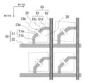
図1は、本実施形態に係る製造方法によって得られる発光モジュールの概略上面図であ
る。図2及び図3は、図1のうち光源20およびその周辺を拡大して示す。図5A及び5
Bは、本実施形態に係る製造方法によって得られる発光モジュールの概略断面図である。
図6は、本実施形態に係る発光モジュールにおける光源の概略断面図である。
発光モジュールは、基板10と、基板10の上面に設けられる複数の光源と、光源の周
囲に設けられる被覆層30と、絶縁部材40と、第1配線50及び第2配線60とを備え
ている。複数の光源20は、複数の行および列を含む二次元状に配置される。複数の光源
20の配置は、二次元状に限定されず、ハニカム状の配置等、任意であってよい。
FIG. 1 is a schematic top view of a light-emitting module obtained by the manufacturing method according to this embodiment. 2 and 3 are enlarged views of the
B is a schematic cross-sectional view of a light-emitting module obtained by the manufacturing method according to this embodiment.
FIG. 6 is a schematic cross-sectional view of the light source in the light emitting module according to this embodiment.
The light emitting module includes a
図1および図2に示す例において、発光モジュール100は、第1方向および第2方向
に沿って光源20が複数配置されている。なお、本明細書において、「第1方向」は、複
数の光源20の行が延びる方向(図1では左右方向)を差し、「第2方向」は、複数の光
源20の列が延びる方向(図1では上下方向)を指す。
In the example shown in FIGS. 1 and 2, the
この例では、光源20のそれぞれは、上面視において正方形状を有している。正方形の
一辺の長さは、例えば15μm以上1000μm以下程度の範囲であり得る。この例では
、発光モジュールの外形も正方形状である。正方形状の発光モジュールの縦方向の長さお
よび横方向の長さは、例えば8cmおよび6cmである。発光モジュール100中の光源
20の数や形状は、任意に設定可能であり、発光モジュール100の形状も任意に設定し
てよい。
In this example, each of the
光源20は、同一面側に正負一対の第1電極23a及び第2電極23bを備える電極形
成面20cと、電極形成面20cと反対側の発光面20aとを有する。光源20は、発光
面20aが基板10の上面に対向するように、直接又は接合部材等を介して配置される。
The
光源20は、発光素子21を有する。発光素子21の発光面21a上に透光性部材22
が設けられている。発光素子21は、透光性接着部材24によって透光性部材22に接着
されている。透光性部材22は、発光素子21の発光面21aを覆うとともに、発光素子
の側面21bよりも外側の領域に広がっている。
The
is provided. The
発光素子21の側面21bは、被覆部材26で覆われている。被覆部材26は、光源2
0の電極形成面20cの一部を構成する。被覆部材26は、発光素子21の第1電極23
a及び第2電極23bの表面が露出するように発光素子21の電極形成面にも設けられて
いる。
A
0 constitutes a part of the
It is also provided on the electrode formation surface of the
被覆層30は、光源20の側面20bを覆うように設けられている。図5A及び5Bに
示す例においては、光源20の電極形成面20cは、被覆層30から露出している。光源
20の電極形成面20cは、第1電極23aおよび第2電極23bが配置される領域以外
を被覆層30で覆っていてもよい。
The
第1配線50は、光源20及び被覆層30の上に配置される。第1配線50は、第1延
伸部51と、第1接続部52とを含む。第1延伸部51は、各光源20の第1電極23a
毎に設けられ、第1電極23aから第2方向に延伸する。第1接続部52は、第1方向に
延伸し、複数の第1延伸部51を電気的に接続する。第1接続部52には、外部端子55
が設けられている。発光モジュールの第1接続部52と第1延伸部51は一体に形成され
ている。
The
, and extends in the second direction from the
is provided. The first connecting
第2配線60は、光源20および被覆層30の上に配置される。第2配線60は、第2
延伸部61と、第2接続部62とを含む。第2延伸部61は、各光源20の第2電極23
b毎に設けられ、第2電極23bから第1方向に延伸する。上面視において、第2延伸部
61の延伸方向における長さは、第2延伸部61の延伸方向と垂直な方向における幅より
も長い。第2延伸部61を第2電極23b上から長く引き出すことにより、複数の第2延
伸部61と接続する第2接続部62を形成する際に、位置合わせを容易に行うことができ
る。
The
It includes an
It is provided every b and extends in the first direction from the
絶縁部材40は、複数の第1接続部52を覆うように設けられている。図5A及び5B
に示す例においては、絶縁部材40は、光源20、第1配線50、第2延伸部61および
被覆層30の上に配置されている。絶縁部材40は、複数の第2延伸部61のそれぞれの
少なくとも一部が露出する開口部を備えている。この開口部は、上面視において、第2電
極23bから離れた位置に設けられている。
第2接続部62は、第2方向に延伸し、絶縁部材40の開口部の位置において、複数の
第2延伸部61を電気的に接続する。第2接続部62には、外部端子55が設けられてい
る(図1参照)。
The insulating
2, the insulating
The second connecting
図4は、図3の光源20およびその周辺をさらに拡大して示す上面図である。図4にお
いて方形状の光源20の電極形成面20cの対向する角部に第1電極23aおよび第2電
極23bが設けられている。図4において、第1電極23aおよび第2電極23bは、直
角三角形であり、方形状である光源20の電極形成面20cの対角線に沿って離隔してい
る。第1延伸部51は、上面視において第1電極23aから第2電極23bとは反対側の
電極形成面20cの角部に向かって延びる第1部分51aと、第2方向に延伸し、第1部
分51aと第1接続部52との間を接続する第2部分51bとを有している。上面視にお
いて、第1部分51aの延伸方向における長さ51aLは、第1部分51aの延伸方向と
垂直な方向における幅51aWよりも長い。また、第2延伸部61は、上面視において第
2電極23bから第1電極23aとは反対側の電極形成面20cの角部に向かって延びる
第3部分61cと、第1方向に延伸し、第3部分61cと第2接続部62との間を接続す
る第4部分61dとを有している。上面視において、第3部分61cの延伸方向における
長さ61cLは、第3部分61cの延伸方向と垂直な方向における幅61cWよりも長い
。これにより、第1延伸部51と第2延伸部61との間でのショートを効果的に防止する
ことができる。なお、第1電極23aおよび第2電極23bの上面視における形状は、三
角形に限定されるものではなく、例えば長方形でもよい。
FIG. 4 is a top view showing the
以下、発光モジュールの製造方法について、図7~図13、図15~図19に示す模式
断面図に基づいて詳細に説明する。
A method for manufacturing a light-emitting module will be described in detail below with reference to schematic cross-sectional views shown in FIGS.
(中間体を準備する工程)
基板10上に、複数の光源20及び被覆層30を配置した中間体90を準備する。
図7に示すように、基板10上に、複数の光源20を配置する。複数の光源20は、基
板10の上面に第1方向および第2方向に沿って配置する。光源20は、電極形成面20
cを上に向け、かつ発光面20aを下に向けた状態で配置する。発光モジュールにおいて
、複数の光源20を所定の間隔を空けて配置する。また、複数の光源20を間隔を空けず
に光源20の側面同士を接触させて配置してもよい。この場合、後述する被覆層30を形
成する工程を省略して、複数の光源20の上に第1配線50および第2配線60を配置す
ることができる。
(Step of preparing an intermediate)
An
As shown in FIG. 7, a plurality of
The
基板10は、光源20を載置することが可能なものである。基板10の形状は、特に限
定されないが、上面が平坦であることが好ましい。基板10と光源20とは、透光性の接
合部材により貼り合わされている。接合部材としては、例えば、エポキシ樹脂等を用いる
ことができる。
The
次に、基板10上であって、光源20の周囲に被覆層30を形成する。被覆層30は、
基板に被覆層30の材料を塗布して設ける。塗布方法は、スピンコータによるスピンコー
ト法、ディスペンサによる吐出など特に限定されない。被覆層30は、例えば、ポリイミ
ド、エポキシ樹脂を用いることができる。
Next, a
A material for the
被覆層30は、基板10及び光源20を覆うように被覆層30の材料を設けた後、光源
20の第1電極23a及び第2電極23bが露出するまで被覆層30の一部を除去するこ
とにより形成することができる。
After providing the material of the
(配線を形成する工程)
得られた中間体の上面に、第1配線50及び第2配線60を含む配線を形成する。配線
を形成する工程は、第1配線50と第2延伸部61とを形成する工程と、絶縁部材40を
形成する工程と、第2接続部62を形成して第2配線を形成する工程とを含む。
(Process of forming wiring)
Wirings including the
(第1配線50と第2延伸部61とを形成する工程)
まず、第1延伸部51と第1接続部52とを含む第1配線50と、第2配線60の一部
である第2延伸部61とを形成する。各々の光源20の第1電極23a及び第2電極23
bの位置を検出し、各々の第1電極23a及び第2電極23bの位置に対応して、第1延
伸部51及び第2延伸部61を形成する。第1配線50及び第2延伸部61は、第1金属
層71及び第2金属層72を積層して形成する。
(Step of Forming
First, the
The position of b is detected, and the first extending
第1配線50と第2延伸部61とを形成する工程においては、まず、図8に示すように
、光源20と被覆層30上の略全面に、第1金属層71をスパッタ等で形成する。第1金
属層71は、後工程である第2金属層72を形成する工程において、第2金属層72を電
解めっき法で形成する際のシード層として用いられる。第1金属層71の積層構造として
は、例えば、基板10側からTi/Cu等が挙げられる。
In the step of forming the
次に、図9に示すように、第1金属層71の上にレジスト81を設ける。レジスト81
は、上面視において、第1延伸部51、第1接続部52及び第2延伸部61に対応した開
口部を有するように形成される。レジスト81は予め検出された第1電極23a及び第2
電極23bの位置に対応して、紫外領域のレーザ光等を用いた直接描画をすることで望ま
しい形状に形成できる。
Next, as shown in FIG. 9, a resist 81 is provided on the
is formed to have openings corresponding to the first extending
A desired shape can be formed by direct drawing using a laser beam or the like in the ultraviolet region corresponding to the position of the
次に、図10に示すように、レジスト81の開口部内に、電解めっき法によって第2金
属層72を形成する。第2金属層72は、第1金属層71を電解めっきのシード層、すな
わち電流経路として用い、レジストの開口部内でめっき成長させることで形成される。第
2金属層72としては、例えば、Cuが挙げられる。
Next, as shown in FIG. 10, the
次に、図11に示すように、レジストを除去して、第1金属層71を露出させる。続い
て、図12に示すように、エッチングにより第2金属層72の一部を除去して薄膜化する
とともに、第2金属層72が形成されていない領域の第1金属層71を除去する。これに
よって、第1金属層71と第2金属層72が積層されてなる第1配線50および第2延伸
部61が形成される。エッチングは、ドライエッチング、ウェットエッチングのいずれで
もよい。
Next, as shown in FIG. 11, the resist is removed to expose the
図2に示すように、光源20が上面視において四角形状である場合、一対の第1電極2
3aおよび第2電極23bの上面視における形状を三角形として、光源20上において対
角に位置するように形成することが好ましい。これにより、小型の光源においても、一対
の第1電極23aおよび第2電極23bを第1方向及び第2方向に広く確保することがで
きるため、その上に形成する一対の第1延伸部51および第2延伸部61と接合する面積
を十分に確保することができる。
As shown in FIG. 2, when the
It is preferable that the shapes of the 3 a and the
(絶縁部材40を形成する工程)
次に、図13に示すように、第1配線50および第2延伸部61の上に、絶縁部材40
を形成する。絶縁部材40は、少なくとも第1接続部52の上であって、第1接続部52
と後述する第2接続部62との間に形成すればよい。図13に示す例では、絶縁部材40
は、第1配線50および第2延伸部61の上に形成する。絶縁部材40の形成後、例えば
フォトリソグラフィによる絶縁部材40のパターニングによって、第1配線50および第
2延伸部61を覆い、かつ、上面視において第2延伸部61に重なる位置に開口部41が
設けられた絶縁部材40を形成する。図14は、絶縁部材40を形成した後の、発光モジ
ュールの一部を拡大して模式的に示す。図14に示すように、絶縁部材40の開口部41
は、第2延伸部61に重なる位置に設けられ、開口部41の位置において、第2延伸部6
1の一部が露出されている。絶縁部材40としては、例えば、シリコーン系、エポキシ系
の感光性の樹脂等を用いることができる。絶縁部材40は、例えばトランスファーモール
ド、圧縮成形、ポッティング、印刷、スプレー等の方法で形成され、光源20および絶縁
層30の上において、第1配線50および第2延伸部61を内部に埋設する厚さ(例えば
2μm~500μm程度)に形成される。
(Step of forming insulating member 40)
Next, as shown in FIG. 13, the insulating
to form The insulating
and a
are formed on the
is provided at a position overlapping the second extending
1 is exposed. As the insulating
(第2接続部62を形成する工程)
次に、複数の第2延伸部61を電気的に接続する第2接続部62を形成する。第2接続
部62は、第3金属層73及び第4金属層74を積層して形成する。
第2接続部62を形成する工程においては、まず、図15に示すように、絶縁部材40
と開口部に露出する第2延伸部61上の略全面に、第3金属層73をスパッタ等で形成す
る。第3金属層73は、後工程である第4金属層74を形成する工程において、第4金属
層74を電解めっき法で形成する際のシード層として用いられる。第3金属層73の積層
構造としては、第1金属層71と同様の材料を用いることができ、例えば、支持部材10
側からTi/Cu等が挙げられる。
(Step of Forming Second Connection Portion 62)
Next, a second connecting
In the step of forming the second connecting
Then, a
Ti/Cu and the like can be mentioned from the side.
次に、図16に示すように、第3金属層73の上にレジスト83を設ける。レジスト8
3は、第2接続部62に対応した開口部84を有するように形成される。
Next, as shown in FIG. 16, a resist 83 is provided on the
3 is formed with an
次に、図17に示すように、レジスト83の開口部84内に、電解めっき法によって第
4金属層74を形成する。第4金属層74は、第3金属層73を電解めっきのシード層、
すなわち電流経路として用い、レジストの開口部内でめっき成長させることで形成される
。第4金属層74としては、第2金属層72と同様の材料を用いることができ、例えば、
Cuが挙げられる。
Next, as shown in FIG. 17, the
That is, it is formed by using it as a current path and growing it by plating within the opening of the resist. As the
Cu is mentioned.
次に、図18に示すように、レジストを除去して、第3金属層73を露出させる。さら
に、エッチングにより第4金属層74の一部を除去して薄膜化するとともに、第4金属層
74が形成されていない領域の第3金属層73を除去する。これによって、図19に示す
ように、第3金属層73と第4金属層74が積層されてなる第2接続部62が形成される
。第2接続部62は、図20に示すように、第2方向に延び、開口部41を介して、第2
の方向に並ぶ第2延伸部61に開口部41の位置で電気的に接続される。これにより、第
2接続部61は、第2方向に並ぶ光源20の第2電極23b同士を電気的に接続する。第
2接続部62を形成する工程において、外部端子55を同時に形成してもよい。
Next, as shown in FIG. 18, the resist is removed to expose the
is electrically connected at the position of the
このようにして、図5A及び5Bに示す構造の発光モジュール100を得ることができ
る。第1配線50の第1延伸部51および第2配線60の第2延伸部61は、光源20の
第1電極23aおよび第2電極23bの位置に対応して形成するため、光源20の第1電
極23aおよび第2電極23bと第1配線50および第2配線60を確実に接続すること
ができる。例えば、図3に示すように光源20を配置する工程等において光源20の位置
ズレが生じたとしても、第1延伸部51の第1部分51aの角度、第2延伸部61の第3
部分61cの角度、第1延伸部51の第2部分51bの長さおよび第2延伸部61の第4
部分61dの長さをそれぞれ変更することで、第1電極23aおよび第2電極23bに対
して第1延伸部51および第2延伸部61を高精度に配置することができる。これにより
、基板上に形成した配線に対して光源の電極を対向させて配置する場合と比較して、光源
20の第1電極23aおよび第2電極23bと第1配線50および第2配線60の位置ズ
レによる接続不良を抑制することができる。第1配線50と第2延伸部61を同一の工程
で形成することにより、製造工程を簡略化することができる。第1配線50と第2延伸部
61を積層することなく設けることができるため、発光モジュールの厚みを低減すること
ができる。また、光源の電極に対して設ける第2延伸部61と、第2接続部62を別の工
程で形成することにより、効率よく第2配線を形成することができる。
Thus, the light-emitting
The angle of the
By changing the length of the
以下、発光モジュールの各構成要素について説明する。 Each component of the light-emitting module will be described below.
(基板10)
基板10は、上面に光源20および被覆層30を配置することが可能なものであれば、
その形状は特に限定されないが、上面が平坦であることが好ましい。基板10は、絶縁性
のものを用いることができる。基板10は、透光性であることが好ましいが、これに限定
されない。基板10としては、例えば、ガラスやセラミック等を用いることが好ましい。
また、基板10として、可撓性を有するものを用いてもよい。基板10の厚みは特に限定
されるものではないが、例えば、0.1mm~1mm程度である。
(Substrate 10)
If the
Although the shape is not particularly limited, it is preferable that the upper surface is flat. An insulating substrate can be used for the
Further, a substrate having flexibility may be used as the
図5A及び5Bに示す例においては、基板10の上面は平坦である。基板10の上面は
必ずしも平坦である必要はなく、上面に各光源20に対応した凹部を設け、その凹部内に
光源20を配置してもよい。
In the example shown in Figures 5A and 5B, the top surface of
(被覆層30)
被覆層30は、光源20の側面を覆っている。被覆層30は、光反射性の材料を用いる
ことができる。光反射性の被覆層30は、光源20から出射される光に対して60%以上
の反射率を有することが好ましく、90%以上の反射率を有することがさらに好ましい。
光反射性の被覆層30の材料は、白色の顔料等を含有させた樹脂を用いることができる。
特に、光反射材(または光散乱材)として酸化チタンを含有させたシリコーン樹脂が好ま
しい。これにより、基板10の一面を被覆するために比較的大量に用いられる材料として
酸化チタンのような安価な原材料を多く用いることで、発光モジュールを安価にすること
ができる。また、被覆層30は、白色の顔料等を含有していない樹脂等の透光性の材料で
形成してもよい。
(Coating layer 30)
The
As a material for the light-
In particular, a silicone resin containing titanium oxide as a light reflecting material (or light scattering material) is preferable. As a result, it is possible to reduce the cost of the light-emitting module by using an inexpensive raw material such as titanium oxide as the material used in a relatively large amount to coat the one surface of the
被覆層30を形成する樹脂材料の母材としては、シリコーン樹脂、フェノール樹脂、エ
ポキシ樹脂、BTレジン、ポリフタルアミド(PPA)等を用いることができる。光反射
材としては、金属の粒子、または、母材よりも高い屈折率を有する無機材料もしくは有機
材料の粒子を用いることができる。光反射材の例は、二酸化チタン、酸化ケイ素、二酸化
ジルコニウム、チタン酸カリウム、酸化アルミニウム、窒化アルミニウム、窒化ホウ素、
ムライト、酸化ニオブ、硫酸バリウムの粒子、または、酸化イットリウムおよび酸化ガド
リニウム等の各種希土類酸化物の粒子等である。
Silicone resin, phenol resin, epoxy resin, BT resin, polyphthalamide (PPA), or the like can be used as the base material of the resin material forming the
Particles of mullite, niobium oxide, barium sulfate, or particles of various rare earth oxides such as yttrium oxide and gadolinium oxide.
(第1配線50、第2配線60)
第1配線50および第2配線60は、光源20の第1電極23aおよび第2電極23b
と電気的に接続される。第1配線50および第2配線60を設けることにより、例えば複
数の光源20同士を電気的に接続することができ、ローカルディミング等に必要な回路を
容易に形成することができる。
(
The
is electrically connected to By providing the
第1配線50および第2配線60の材料としては、電気抵抗が低い材料が好ましく、C
u、Au及びAlよりなる群から選択される少なくとも一つを含むものが挙げられる。な
かでも、Cuを用いることが好ましい。第1配線50および第2配線60の厚みは特に限
定されるものではないが、例えば、10nm~100μm程度である。
As a material for the
Examples include those containing at least one selected from the group consisting of u, Au and Al. Among them, it is preferable to use Cu. Although the thickness of the
(光源20)
図6に示す例では、光源は、発光素子21に加えて、透光性部材22、透光性接着部材
24、被覆部材26を含む。光源は、透光性部材22、透光性接着部材24及び被覆部材
26を省略して、発光素子21のみで構成してもよい。光源20の厚みは特に限定される
ものではないが、例えば、100μm~1mm程度である。
(Light source 20)
In the example shown in FIG. 6, the light source includes a
(発光素子21)
発光素子21は、一対の電極を同じ面側に設けている。発光素子21は、窒化物半導体
等から構成される既知の半導体発光素子を適用できる。また、発光素子21は、所望の発
光色を得るために任意の波長のものを選択することができる。
(Light emitting element 21)
The
発光素子21としては、様々な発光波長の発光ダイオードを利用することができる。ま
た、所望の発光色を得るために、後述する蛍光体と組み合わせてもよい。特に、白色の発
光を得るには、青色を発光する窒化物半導体発光素子と、青色光を吸収して黄色光や緑色
光や赤色光を発する蛍光体とを組み合わせることが好ましい。
As the
(透光性部材22)
透光性部材22は、発光素子21の発光面21aに設けられる。透光性部材22として
は、透明樹脂、ガラス等を用いることができる。透明樹脂としては、耐久性、成形のしや
すさ等の観点から、シリコーン樹脂等を用いることが好ましい。
図21に示すように、光源20における透光性部材22は、発光素子21の上面、つま
り発光面21aと側面21bを覆っていてもよい。
(translucent member 22)
The
As shown in FIG. 21, the
透光性部材22は、波長変換部材を含有させることができる。波長変換部材は、発光素
子21からの光を吸収して他の波長の光を発光することが可能な蛍光体を含む。これによ
り、発光モジュール100は、発光素子21からの光と波長変換部材で波長変換された光
との混色光、例えば、白色光を外部に出射することができる。発光素子21の種類及び蛍
光体の種類を選択することにより、出射光の色を適宜調整することができる。蛍光体は、
発光素子21が発する光によって励起され、発光素子21が発する光の波長とは異なる波
長の光を発する。例えば、蛍光体として、YAG蛍光体、βサイアロン蛍光体、KSF系
蛍光体又はMGF系蛍光体等のフッ化物系蛍光体、CASN系蛍光体等の窒化物蛍光体な
どを用いることができる。透光性部材22は、複数種類の蛍光体を含んでいてもよい。ま
た、上記蛍光体の層を複数積層させてもよい。
The
It is excited by the light emitted by the
また、発光モジュール100の上面または下面に波長変換シートを設けてもよい。波長
変換シートは、典型的には、蛍光体の粒子が分散されたシート状の樹脂である。このよう
な波長変換シートを用いることにより、発光モジュール100の上面または下面に蛍光体
を均一に配置することができる。このような構成においては、透光性部材22が蛍光体等
を含有することは必須ではない。
Also, a wavelength conversion sheet may be provided on the upper surface or the lower surface of the
100 発光モジュール
10 基板
20 光源
21 発光素子
21a 発光面
21b 側面
22 透光性部材
23a 第1電極
23b 第2電極
24 透光性接着部材
26 被覆部材
30 被覆層
40 絶縁部材
50 第1配線
51 第1延伸部
52 第1接続部
55 外部端子
60 第2配線
61 第2延伸部
62 第2接続部
71 第1金属層
72 第2金属層
73 第3金属層
74 第4金属層
81、83 レジスト
84 開口部
90 中間体
REFERENCE SIGNS
Claims (8)
前記基板の一方の主面上に、第1方向および前記第1方向とは異なる第2方向に沿って
配置され、上面側に露出する第1電極及び第2電極を備える複数の光源、
前記第1電極毎に設けられ、前記第1電極から前記第2方向に延伸する第1延伸部と、
前記第1方向に延伸し、複数の前記第1延伸部と電気的に接続する第1接続部とを含む第
1配線、
前記第2電極毎に設けられ、前記第2電極から前記第1方向に延伸する第2延伸部と、
前記第2方向に延伸し、複数の前記第2延伸部と電気的に接続する第2接続部とを含む第
2配線、及び
前記複数の第1延伸部、複数の前記第1接続部及び複数の前記第2延伸部を覆い、複数
の前記第2延伸部のそれぞれの一部を露出する複数の開口部を有する絶縁部材を備え、
前記第2接続部は、前記第1接続部上の前記絶縁部材上に配置され、前記開口部におい
て、複数の前記第2延伸部のそれぞれと接続している発光モジュール。 substrate,
a plurality of light sources arranged on one main surface of the substrate along a first direction and a second direction different from the first direction, and comprising a first electrode and a second electrode exposed on the upper surface side;
a first extending portion provided for each of the first electrodes and extending from the first electrodes in the second direction;
a first wiring extending in the first direction and including a first connecting portion electrically connected to the plurality of first extending portions;
a second extending portion provided for each second electrode and extending from the second electrode in the first direction;
a second wiring extending in the second direction and including a second connecting portion electrically connected to the plurality of second extending portions; and the plurality of first extending portions, the plurality of first connecting portions, and the plurality of second wirings an insulating member having a plurality of openings that cover the second extending portions of and expose a portion of each of the plurality of second extending portions;
The second connection portion is arranged on the insulating member on the first connection portion, and is connected to each of the plurality of second extension portions at the opening.
方向に延伸する第2部分とを含む請求項1に記載の発光モジュール。 2. The light emitting module according to claim 1, wherein the first extending portion includes a first portion extending in a predetermined direction and a second portion extending in a direction different from the extending direction of the first portion.
と垂直な方向における幅Wよりも長い請求項2に記載の発光モジュール。 3. The light-emitting module according to claim 2 , wherein, when viewed from above, the length L in the extending direction of the first portion is longer than the width W in the direction perpendicular to the extending direction of the first portion.
方向に延伸する第4部分とを含む請求項1に記載の発光モジュール。 2. The light emitting module according to claim 1, wherein the second extending portion includes a third portion extending in a predetermined direction and a fourth portion extending in a direction different from the extending direction of the third portion.
と垂直な方向における幅Wよりも長い請求項4に記載の発光モジュール。 5. The light-emitting module according to claim 4 , wherein, when viewed from above, the length L of the third portion in the extending direction is longer than the width W of the third portion in the direction perpendicular to the extending direction.
前記第1電極及び前記第2電極は、上面視において、それぞれ三角形状であり、前記光
源の上面側において対角に位置するように配置されている請求項1に記載の発光モジュー
ル。 The light source has a rectangular shape in top view,
2. The light-emitting module according to claim 1, wherein the first electrode and the second electrode each have a triangular shape when viewed from above, and are arranged so as to be positioned diagonally on the upper surface side of the light source.
載の発光モジュール。 2. The light-emitting module according to claim 1, wherein the first extending portion and the first connecting portion are made of the same metal layer.
の発光モジュール。 2. The light emitting module according to claim 1, further comprising a coating layer on the substrate and coating the periphery of the light source.
Applications Claiming Priority (3)
| Application Number | Priority Date | Filing Date | Title |
|---|---|---|---|
| JP2020015089 | 2020-01-31 | ||
| JP2020015089 | 2020-01-31 | ||
| JP2021006953A JP7054031B2 (en) | 2020-01-31 | 2021-01-20 | Manufacturing method of light emitting module |
Related Parent Applications (1)
| Application Number | Title | Priority Date | Filing Date |
|---|---|---|---|
| JP2021006953A Division JP7054031B2 (en) | 2020-01-31 | 2021-01-20 | Manufacturing method of light emitting module |
Publications (3)
| Publication Number | Publication Date |
|---|---|
| JP2022088567A JP2022088567A (en) | 2022-06-14 |
| JP2022088567A5 JP2022088567A5 (en) | 2022-07-28 |
| JP7273349B2 true JP7273349B2 (en) | 2023-05-15 |
Family
ID=77062359
Family Applications (1)
| Application Number | Title | Priority Date | Filing Date |
|---|---|---|---|
| JP2022056501A Active JP7273349B2 (en) | 2020-01-31 | 2022-03-30 | light emitting module |
Country Status (2)
| Country | Link |
|---|---|
| US (2) | US11508891B2 (en) |
| JP (1) | JP7273349B2 (en) |
Families Citing this family (1)
| Publication number | Priority date | Publication date | Assignee | Title |
|---|---|---|---|---|
| DE102022103970A1 (en) | 2022-02-21 | 2023-08-24 | Ams-Osram International Gmbh | DISPLAY UNIT, DISPLAY DEVICE AND METHOD OF MAKING A DISPLAY UNIT |
Citations (4)
| Publication number | Priority date | Publication date | Assignee | Title |
|---|---|---|---|---|
| WO2006035664A1 (en) | 2004-09-27 | 2006-04-06 | Matsushita Electric Industrial Co., Ltd. | Semiconductor light emitting element, manufacturing method and mounting method of the same and light emitting device |
| JP2009302542A (en) | 2008-06-13 | 2009-12-24 | Samsung Electronics Co Ltd | Light emitting element, light emitting device including light emitting element, method for manufacturing light emitting element, and method for manufacturing light emitting device including light emitting element |
| JP2019197132A (en) | 2018-05-09 | 2019-11-14 | 住宅環境設備株式会社 | Display device |
| JP2020009906A (en) | 2018-07-09 | 2020-01-16 | 日亜化学工業株式会社 | Manufacturing method of light emitting module |
Family Cites Families (4)
| Publication number | Priority date | Publication date | Assignee | Title |
|---|---|---|---|---|
| JP2002329896A (en) | 2001-05-02 | 2002-11-15 | Kansai Tlo Kk | Led surface light emission device |
| KR100928259B1 (en) * | 2007-10-15 | 2009-11-24 | 엘지전자 주식회사 | Light emitting device and manufacturing method thereof |
| KR20130128841A (en) * | 2012-05-18 | 2013-11-27 | 삼성전자주식회사 | Semiconductor light emitting device having a multi-cell array and manufacturing method for the same, light emitting module and illumination apparatus |
| TWI597872B (en) * | 2013-11-25 | 2017-09-01 | 晶元光電股份有限公司 | Light-emitting diode device |
-
2021
- 2021-01-28 US US17/161,402 patent/US11508891B2/en active Active
-
2022
- 2022-03-30 JP JP2022056501A patent/JP7273349B2/en active Active
- 2022-10-20 US US18/048,404 patent/US11777069B2/en active Active
Patent Citations (4)
| Publication number | Priority date | Publication date | Assignee | Title |
|---|---|---|---|---|
| WO2006035664A1 (en) | 2004-09-27 | 2006-04-06 | Matsushita Electric Industrial Co., Ltd. | Semiconductor light emitting element, manufacturing method and mounting method of the same and light emitting device |
| JP2009302542A (en) | 2008-06-13 | 2009-12-24 | Samsung Electronics Co Ltd | Light emitting element, light emitting device including light emitting element, method for manufacturing light emitting element, and method for manufacturing light emitting device including light emitting element |
| JP2019197132A (en) | 2018-05-09 | 2019-11-14 | 住宅環境設備株式会社 | Display device |
| JP2020009906A (en) | 2018-07-09 | 2020-01-16 | 日亜化学工業株式会社 | Manufacturing method of light emitting module |
Also Published As
| Publication number | Publication date |
|---|---|
| US20210242382A1 (en) | 2021-08-05 |
| US11777069B2 (en) | 2023-10-03 |
| US11508891B2 (en) | 2022-11-22 |
| JP2022088567A (en) | 2022-06-14 |
| US20230066932A1 (en) | 2023-03-02 |
Similar Documents
| Publication | Publication Date | Title |
|---|---|---|
| US10128421B2 (en) | Light emitting device | |
| US20220209080A1 (en) | Light emitting device | |
| US11092731B2 (en) | Light emitting module and planar light source having a light guide with cavity and flourescent material disposed on a surface of cavity and light guide | |
| JP6680311B2 (en) | Light emitting device and surface emitting light source | |
| JP7189451B2 (en) | Light emitting module, liquid crystal display | |
| JP7273349B2 (en) | light emitting module | |
| US10797210B2 (en) | Light emitting device having reduced thickness and increased light-reflectivity | |
| JP2017118081A (en) | Light-emitting device | |
| US11640957B2 (en) | Light emitting module | |
| KR20170095016A (en) | Semiconductor light emitting device package | |
| JP7025660B2 (en) | Luminescent device | |
| JP7054031B2 (en) | Manufacturing method of light emitting module | |
| JP7004948B2 (en) | Manufacturing method of light emitting module | |
| JP7140999B2 (en) | Planar light source and manufacturing method thereof | |
| JP7057526B2 (en) | Luminous module | |
| JP7116327B2 (en) | Light-emitting module and method for manufacturing light-emitting module | |
| US11650457B2 (en) | Demarcating member, demarcating structure body, surface light source, and liquid-crystal display device | |
| JP7314474B2 (en) | planar light source | |
| JP7148810B2 (en) | Light-emitting module manufacturing method and light-emitting module | |
| JP2022129961A (en) | Light emitting device and planar light source | |
| JP2023149603A (en) | Surface light source, liquid crystal display device | |
| JP2023081081A (en) | Manufacturing method of planer light source and planer light source |
Legal Events
| Date | Code | Title | Description |
|---|---|---|---|
| A521 | Request for written amendment filed |
Free format text: JAPANESE INTERMEDIATE CODE: A523 Effective date: 20220720 |
|
| A621 | Written request for application examination |
Free format text: JAPANESE INTERMEDIATE CODE: A621 Effective date: 20220721 |
|
| A977 | Report on retrieval |
Free format text: JAPANESE INTERMEDIATE CODE: A971007 Effective date: 20230215 |
|
| A131 | Notification of reasons for refusal |
Free format text: JAPANESE INTERMEDIATE CODE: A131 Effective date: 20230221 |
|
| A521 | Request for written amendment filed |
Free format text: JAPANESE INTERMEDIATE CODE: A523 Effective date: 20230306 |
|
| TRDD | Decision of grant or rejection written | ||
| A01 | Written decision to grant a patent or to grant a registration (utility model) |
Free format text: JAPANESE INTERMEDIATE CODE: A01 Effective date: 20230328 |
|
| A61 | First payment of annual fees (during grant procedure) |
Free format text: JAPANESE INTERMEDIATE CODE: A61 Effective date: 20230410 |
|
| R151 | Written notification of patent or utility model registration |
Ref document number: 7273349 Country of ref document: JP Free format text: JAPANESE INTERMEDIATE CODE: R151 |