JP7264352B2 - トポロジカル絶縁体レーザーシステム - Google Patents
トポロジカル絶縁体レーザーシステム Download PDFInfo
- Publication number
- JP7264352B2 JP7264352B2 JP2020503106A JP2020503106A JP7264352B2 JP 7264352 B2 JP7264352 B2 JP 7264352B2 JP 2020503106 A JP2020503106 A JP 2020503106A JP 2020503106 A JP2020503106 A JP 2020503106A JP 7264352 B2 JP7264352 B2 JP 7264352B2
- Authority
- JP
- Japan
- Prior art keywords
- array
- optical
- topological
- laser system
- resonators
- Prior art date
- Legal status (The legal status is an assumption and is not a legal conclusion. Google has not performed a legal analysis and makes no representation as to the accuracy of the status listed.)
- Active
Links
Images


Classifications
-
- H—ELECTRICITY
- H01—ELECTRIC ELEMENTS
- H01S—DEVICES USING THE PROCESS OF LIGHT AMPLIFICATION BY STIMULATED EMISSION OF RADIATION [LASER] TO AMPLIFY OR GENERATE LIGHT; DEVICES USING STIMULATED EMISSION OF ELECTROMAGNETIC RADIATION IN WAVE RANGES OTHER THAN OPTICAL
- H01S5/00—Semiconductor lasers
- H01S5/40—Arrangement of two or more semiconductor lasers, not provided for in groups H01S5/02 - H01S5/30
- H01S5/4025—Array arrangements, e.g. constituted by discrete laser diodes or laser bar
- H01S5/4031—Edge-emitting structures
- H01S5/4043—Edge-emitting structures with vertically stacked active layers
- H01S5/405—Two-dimensional arrays
-
- G—PHYSICS
- G02—OPTICS
- G02B—OPTICAL ELEMENTS, SYSTEMS OR APPARATUS
- G02B6/00—Light guides; Structural details of arrangements comprising light guides and other optical elements, e.g. couplings
- G02B6/10—Light guides; Structural details of arrangements comprising light guides and other optical elements, e.g. couplings of the optical waveguide type
- G02B6/12—Light guides; Structural details of arrangements comprising light guides and other optical elements, e.g. couplings of the optical waveguide type of the integrated circuit kind
- G02B6/122—Basic optical elements, e.g. light-guiding paths
- G02B6/1225—Basic optical elements, e.g. light-guiding paths comprising photonic band-gap structures or photonic lattices
-
- H—ELECTRICITY
- H01—ELECTRIC ELEMENTS
- H01S—DEVICES USING THE PROCESS OF LIGHT AMPLIFICATION BY STIMULATED EMISSION OF RADIATION [LASER] TO AMPLIFY OR GENERATE LIGHT; DEVICES USING STIMULATED EMISSION OF ELECTROMAGNETIC RADIATION IN WAVE RANGES OTHER THAN OPTICAL
- H01S5/00—Semiconductor lasers
- H01S5/02—Structural details or components not essential to laser action
- H01S5/022—Mountings; Housings
- H01S5/0225—Out-coupling of light
- H01S5/02251—Out-coupling of light using optical fibres
-
- H—ELECTRICITY
- H01—ELECTRIC ELEMENTS
- H01S—DEVICES USING THE PROCESS OF LIGHT AMPLIFICATION BY STIMULATED EMISSION OF RADIATION [LASER] TO AMPLIFY OR GENERATE LIGHT; DEVICES USING STIMULATED EMISSION OF ELECTROMAGNETIC RADIATION IN WAVE RANGES OTHER THAN OPTICAL
- H01S5/00—Semiconductor lasers
- H01S5/04—Processes or apparatus for excitation, e.g. pumping, e.g. by electron beams
- H01S5/041—Optical pumping
-
- H—ELECTRICITY
- H01—ELECTRIC ELEMENTS
- H01S—DEVICES USING THE PROCESS OF LIGHT AMPLIFICATION BY STIMULATED EMISSION OF RADIATION [LASER] TO AMPLIFY OR GENERATE LIGHT; DEVICES USING STIMULATED EMISSION OF ELECTROMAGNETIC RADIATION IN WAVE RANGES OTHER THAN OPTICAL
- H01S5/00—Semiconductor lasers
- H01S5/10—Construction or shape of the optical resonator, e.g. extended or external cavity, coupled cavities, bent-guide, varying width, thickness or composition of the active region
- H01S5/1021—Coupled cavities
-
- H—ELECTRICITY
- H01—ELECTRIC ELEMENTS
- H01S—DEVICES USING THE PROCESS OF LIGHT AMPLIFICATION BY STIMULATED EMISSION OF RADIATION [LASER] TO AMPLIFY OR GENERATE LIGHT; DEVICES USING STIMULATED EMISSION OF ELECTROMAGNETIC RADIATION IN WAVE RANGES OTHER THAN OPTICAL
- H01S5/00—Semiconductor lasers
- H01S5/10—Construction or shape of the optical resonator, e.g. extended or external cavity, coupled cavities, bent-guide, varying width, thickness or composition of the active region
- H01S5/1071—Ring-lasers
-
- H—ELECTRICITY
- H01—ELECTRIC ELEMENTS
- H01S—DEVICES USING THE PROCESS OF LIGHT AMPLIFICATION BY STIMULATED EMISSION OF RADIATION [LASER] TO AMPLIFY OR GENERATE LIGHT; DEVICES USING STIMULATED EMISSION OF ELECTROMAGNETIC RADIATION IN WAVE RANGES OTHER THAN OPTICAL
- H01S5/00—Semiconductor lasers
- H01S5/30—Structure or shape of the active region; Materials used for the active region
- H01S5/34—Structure or shape of the active region; Materials used for the active region comprising quantum well or superlattice structures, e.g. single quantum well [SQW] lasers, multiple quantum well [MQW] lasers or graded index separate confinement heterostructure [GRINSCH] lasers
- H01S5/343—Structure or shape of the active region; Materials used for the active region comprising quantum well or superlattice structures, e.g. single quantum well [SQW] lasers, multiple quantum well [MQW] lasers or graded index separate confinement heterostructure [GRINSCH] lasers in AIIIBV compounds, e.g. AlGaAs-laser, InP-based laser
- H01S5/34333—Structure or shape of the active region; Materials used for the active region comprising quantum well or superlattice structures, e.g. single quantum well [SQW] lasers, multiple quantum well [MQW] lasers or graded index separate confinement heterostructure [GRINSCH] lasers in AIIIBV compounds, e.g. AlGaAs-laser, InP-based laser with a well layer based on Ga(In)N or Ga(In)P, e.g. blue laser
-
- H—ELECTRICITY
- H01—ELECTRIC ELEMENTS
- H01S—DEVICES USING THE PROCESS OF LIGHT AMPLIFICATION BY STIMULATED EMISSION OF RADIATION [LASER] TO AMPLIFY OR GENERATE LIGHT; DEVICES USING STIMULATED EMISSION OF ELECTROMAGNETIC RADIATION IN WAVE RANGES OTHER THAN OPTICAL
- H01S5/00—Semiconductor lasers
- H01S5/40—Arrangement of two or more semiconductor lasers, not provided for in groups H01S5/02 - H01S5/30
- H01S5/4025—Array arrangements, e.g. constituted by discrete laser diodes or laser bar
-
- H—ELECTRICITY
- H01—ELECTRIC ELEMENTS
- H01S—DEVICES USING THE PROCESS OF LIGHT AMPLIFICATION BY STIMULATED EMISSION OF RADIATION [LASER] TO AMPLIFY OR GENERATE LIGHT; DEVICES USING STIMULATED EMISSION OF ELECTROMAGNETIC RADIATION IN WAVE RANGES OTHER THAN OPTICAL
- H01S2301/00—Functional characteristics
- H01S2301/16—Semiconductor lasers with special structural design to influence the modes, e.g. specific multimode
- H01S2301/166—Single transverse or lateral mode
-
- H—ELECTRICITY
- H01—ELECTRIC ELEMENTS
- H01S—DEVICES USING THE PROCESS OF LIGHT AMPLIFICATION BY STIMULATED EMISSION OF RADIATION [LASER] TO AMPLIFY OR GENERATE LIGHT; DEVICES USING STIMULATED EMISSION OF ELECTROMAGNETIC RADIATION IN WAVE RANGES OTHER THAN OPTICAL
- H01S3/00—Lasers, i.e. devices using stimulated emission of electromagnetic radiation in the infrared, visible or ultraviolet wave range
- H01S3/05—Construction or shape of optical resonators; Accommodation of active medium therein; Shape of active medium
- H01S3/06—Construction or shape of active medium
- H01S3/063—Waveguide lasers, i.e. whereby the dimensions of the waveguide are of the order of the light wavelength
- H01S3/0632—Thin film lasers in which light propagates in the plane of the thin film
- H01S3/0637—Integrated lateral waveguide, e.g. the active waveguide is integrated on a substrate made by Si on insulator technology (Si/SiO2)
-
- H—ELECTRICITY
- H01—ELECTRIC ELEMENTS
- H01S—DEVICES USING THE PROCESS OF LIGHT AMPLIFICATION BY STIMULATED EMISSION OF RADIATION [LASER] TO AMPLIFY OR GENERATE LIGHT; DEVICES USING STIMULATED EMISSION OF ELECTROMAGNETIC RADIATION IN WAVE RANGES OTHER THAN OPTICAL
- H01S3/00—Lasers, i.e. devices using stimulated emission of electromagnetic radiation in the infrared, visible or ultraviolet wave range
- H01S3/23—Arrangements of two or more lasers not provided for in groups H01S3/02 - H01S3/22, e.g. tandem arrangements of separate active media
- H01S3/2383—Parallel arrangements
-
- H—ELECTRICITY
- H01—ELECTRIC ELEMENTS
- H01S—DEVICES USING THE PROCESS OF LIGHT AMPLIFICATION BY STIMULATED EMISSION OF RADIATION [LASER] TO AMPLIFY OR GENERATE LIGHT; DEVICES USING STIMULATED EMISSION OF ELECTROMAGNETIC RADIATION IN WAVE RANGES OTHER THAN OPTICAL
- H01S5/00—Semiconductor lasers
- H01S5/10—Construction or shape of the optical resonator, e.g. extended or external cavity, coupled cavities, bent-guide, varying width, thickness or composition of the active region
- H01S5/11—Comprising a photonic bandgap structure
Landscapes
- Physics & Mathematics (AREA)
- General Physics & Mathematics (AREA)
- Optics & Photonics (AREA)
- Condensed Matter Physics & Semiconductors (AREA)
- Electromagnetism (AREA)
- Engineering & Computer Science (AREA)
- Microelectronics & Electronic Packaging (AREA)
- Lasers (AREA)
- Semiconductor Lasers (AREA)
- Optical Integrated Circuits (AREA)
Description
さらに、環境、欠陥、製造の不完全性、および励起パワーの変化に対して、堅牢な放射を有するレーザーアレイ配置が必要とされている。
ゲイン材料を含む光学素子を含む光学素子アレイであって、アレイの光学素子が、それらの間で光学的に結合され、アレイの特定の空間領域に関連する少なくとも1つのトポロジカルモードを維持するように空間的に配置された光学素子アレイ;
該トポロジカルモードに対応する空間領域の少なくとも一部内のアレイの一群の光学素子の励起を可能とするように構成された励起ユニット;および
該トポロジカルモードに関連する1つまたは複数の光学素子に光学的に結合された少なくとも1つの出力ポートであって、該レーザーシステムからの光強度の一部を抽出するように構成された出力ポート
を備える。
六角形格子に配置され、複数の六角形配置を規定し、該六角形配置内の第1の結合比および第1の結合比より小さい隣接六角形配置間の第2の結合比を特徴とする光共振器アレイであって、該共振器の共振周波数に関連する波長帯で光学的放射を行うように構成されたゲイン材料を有する光共振器含む光共振器アレイ;
該アレイのエッジに沿って、少なくとも一部に励起エネルギーを供給するように構成された励起ユニット;ならびに
該アレイのエッジに沿って1つまたは複数の共振器に結合した光学的導波管を含む少なくとも1つの出力ポート
を備える。
第1の共振周波数を特徴とする光共振器アレイ、および第1の共振周波数とは異なる第2の共振周波数を有する複数のリンクカプラーであって、該リンク共振器がアレイにより規定される格子ベクトルに沿って隣接共振器間に配置され、該リンクカプラーが該第1の共振周波数で隣接共振器に強く結合され、該光共振器が、該第1の共振周波数に対応する波長で光を放出するように構成されたゲイン材料を有する光共振器を含む、光共振器アレイおよびリンクカプラー;
該アレイのエッジに沿って、少なくとも一部に励起エネルギーを供給するように構成された励起ユニット;ならびに
該アレイのエッジに沿って1つまたは複数の共振器に結合した光学的導波管を含む少なくとも1つの出力ポート
を備える。
ゲイン材料を有する光学素子を含む光学素子アレイであって、アレイの光学素子がそれらの間で光学的に結合され、アレイがアレイの特定の空間領域に関連する少なくとも1つのトポロジカルモードを維持するように空間的に収容された光学素子アレイ;
該トポロジカルモードに対応する空間領域の少なくとも一部内のアレイの一群の光学素子の励起を可能とするように構成された励起ユニット;および
該トポロジカルモードに関連する1つまたは複数の光学素子に光学的に結合された少なくとも1つの出力ポートであって、該レーザーシステムからの光強度の一部を抽出するように構成された出力ポート
を備える。

式中、
Claims (15)
- レーザーシステムであって、
ある共振範囲を有する光共振器のアレイにより形成されたある配列の単位格子を備えるアレイ構造であって、前記アレイ構造の光共振器は、前記光共振器に隣接する導波管の形態にある光リンクによりそれらの間で光学的に結合され、前記光共振器は、前記光共振器の共振範囲と重なり合う1つ以上の波長範囲内での放出による励起エネルギーに応答することができる非線形の光学ゲインを有する選択されたゲイン媒体から作られた半導性導波管として構成され、前記光共振器および前記光リンクは行をなして配列され、前記行の光リンクは、隣り合う行の光リンクに対して所定のシフト量をもって配列され、それにより、反時計回り方向に結合された光に対して時計回り方向にある光共振器間に連結された光により蓄積された位相シフトの変動を誘導し、その結果、前記励起エネルギーが、前記アレイ構造のエッジ領域の少なくとも一部の中に配列された光共振器に印加されるときに、少なくとも1つのトポロジカルに保護されたエッジモードが創出され、前記アレイ構造のエッジ領域の周りで単一方向に伝播し、前記エッジ領域の周りで均一に広がり、前記アレイ構造は、それにより、前記アレイ構造のエッジ領域内で前記光共振器の単一レージングモードを与えるトポロジカル絶縁体として構成される、アレイ構造と、
前記アレイ構造のエッジ領域の少なくとも一部の中で前記光共振器を励起するために前記励起エネルギーを与えるように構成された励起ユニットと、
レーザー出力を規定する少なくとも1つの出力カプラーであって、前記少なくとも1つの出力カプラーは、前記アレイ構造のエッジ領域にて前記光共振器のうち何れか1つ以上に光学的に結合され、それにより、前記レーザーシステムからの光強度の一部を抽出するべく、前記エッジ領域の周りで単一方向に伝播する単一レージングモードの、前記少なくとも1つの出力カプラーのそれぞれの中への強い結合を与える、出力カプラーと、
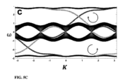
を備える、レーザーシステム。 - 前記光共振器のアレイがフォトニック結晶として構成され、前記フォトニック結晶が、前記フォトニック結晶内のフォトニック状態に関連するバンド構造を有し、前記バンド構造が、前記フォトニック状態のバンド間のギャップと交差する1つ以上のフォトニック状態を備え、前記ギャップと交差する1つ以上のフォトニック状態が、前記アレイ構造のエッジ領域内の少なくとも1つのトポロジカルエッジモードに対応する、請求項1に記載のレーザーシステム。
- 前記アレイが二次元アレイである、請求項1または2に記載のレーザーシステム。
- 前記アレイの光共振器を結合する光リンクが、前記隣り合う行の光共振器間の結合が、選択された位相シフトを一方の方向における光結合に対して導入し、異なる位相シフトを逆方向における光結合に対して導入するように構成される、請求項1乃至3のいずれか1項に記載のレーザーシステム。
- 前記光共振器がリング共振器である、請求項1乃至4のいずれか1項に記載のレーザーシステム。
- 前記光共振器が、少なくとも1つのヘリカル部分を備える、請求項1乃至5のいずれか1項に記載のレーザーシステム。
- 前記単位格子のそれぞれが、前記光共振器間に少なくとも2つの光リンク結合を備え、前記光リンクが、対応する光共振器間の軸に対して選択された空間シフトをもって調節され、それにより、前記光リンクを介して前記光共振器を連結する2つの光路に関連する位相差を与える、請求項1乃至6のいずれか1項に記載のレーザーシステム。
- 前記光リンクが、対応する光共振器間の軸に対するシフトをもって配列され、前記シフトが、前記アレイ構造の別の行間で変化する、請求項7に記載のレーザーシステム。
- 前記光リンクの位置におけるシフトが、前記アレイ構造の別の行間の所定のステップレベルにより変化する、請求項8に記載のレーザーシステム。
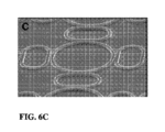
- 前記光共振器が、複数の六角形配列を規定する六角形格子内に配列され、前記六角形配列は、前記六角形配列内の第1の結合定数および隣り合う六角形配列間の第2の結合定数を特徴とし、前記第2の結合定数は、前記第1の結合定数に比べて小さい、請求項1乃至9のいずれか1項に記載のレーザーシステム。
- 前記アレイの隣り合う光共振器間にそれらの間の結合を与えるように配置された光リンクが、前記光共振器の共振範囲に対して共振せず、かつ/または損失が大きいように構成される、請求項1乃至10のいずれか1項に記載のレーザーシステム。
- 前記アレイ構造が、矩形格子、六角格子、およびハニカム格子から選択されるか、または各ユニットがハニカム格子で形成されるサブアレイユニットの三角格子を有する格子形状を有する、請求項1乃至11のいずれか1項に記載のレーザーシステム。
- 前記ゲイン材料が、少なくとも1種の窒化物化合物を備える、請求項1乃至12のいずれか1項に記載のレーザーシステム。
- 前記窒化物化合物が、少なくとも1種のガリウム含有層を備える、請求項13に記載のレーザーシステム。
- 前記光共振器が、前記ゲイン媒体として機能するInGaAsP量子井戸を備える、請求項1乃至14のいずれか1項に記載のレーザーシステム。
Applications Claiming Priority (5)
| Application Number | Priority Date | Filing Date | Title |
|---|---|---|---|
| US201762480604P | 2017-04-03 | 2017-04-03 | |
| US62/480,604 | 2017-04-03 | ||
| US201862624196P | 2018-01-31 | 2018-01-31 | |
| US62/624,196 | 2018-01-31 | ||
| PCT/IL2018/050375 WO2018185749A1 (en) | 2017-04-03 | 2018-03-29 | Topological insulator laser system |
Publications (2)
| Publication Number | Publication Date |
|---|---|
| JP2020516084A JP2020516084A (ja) | 2020-05-28 |
| JP7264352B2 true JP7264352B2 (ja) | 2023-04-25 |
Family
ID=63713356
Family Applications (1)
| Application Number | Title | Priority Date | Filing Date |
|---|---|---|---|
| JP2020503106A Active JP7264352B2 (ja) | 2017-04-03 | 2018-03-29 | トポロジカル絶縁体レーザーシステム |
Country Status (4)
| Country | Link |
|---|---|
| US (1) | US11283244B2 (ja) |
| EP (1) | EP3607371A4 (ja) |
| JP (1) | JP7264352B2 (ja) |
| WO (1) | WO2018185749A1 (ja) |
Families Citing this family (14)
| Publication number | Priority date | Publication date | Assignee | Title |
|---|---|---|---|---|
| DE102016014939B4 (de) * | 2016-12-14 | 2025-10-09 | Forschungsverbund Berlin E.V. | Laservorrichtung, basierend auf einem photonischen Kristall mit säulen- oder wandförmigen Halbleiterelementen, und Verfahren zu deren Betrieb und Herstellung |
| WO2020198321A1 (en) * | 2019-03-25 | 2020-10-01 | The Regents Of The University Of California | System and method for topological lasers generating and multiplexing optical beams with unbounded orbital angular momenta |
| WO2021010894A1 (en) * | 2019-07-15 | 2021-01-21 | Nanyang Technological University | Laser source and method for forming the same |
| US12181772B2 (en) * | 2019-09-12 | 2024-12-31 | The Trustees Of The University Of Pennsylvania | Optical switch device configured for topological light steering and related methods |
| US12531394B2 (en) | 2019-10-28 | 2026-01-20 | Institute Of Physics, Chinese Academy Of Sciences | Topological photonic crystal cavity and its application in lasers |
| CN110932091B (zh) * | 2019-12-06 | 2020-10-09 | 北京大学 | 一种基于能带反转光场限制效应的拓扑体态激光器及方法 |
| JP7684644B2 (ja) | 2020-04-27 | 2025-05-28 | テクニオン リサーチ アンド ディベロップメント ファウンデイション リミテッド | トポロジー絶縁体表面発光レーザシステム |
| CN113204130B (zh) * | 2021-04-27 | 2022-05-20 | 北京大学 | 一种基于非厄米效应的二维可控拓扑态器件及其实现方法 |
| CN113285346A (zh) * | 2021-05-14 | 2021-08-20 | 北京邮电大学 | 一种基于拓扑光子的半导体涡旋光激光器 |
| CN114069389B (zh) * | 2021-11-16 | 2024-07-09 | 深圳斯玛特传感技术有限公司 | 一种量子级联激光器 |
| WO2023163649A1 (en) * | 2022-02-28 | 2023-08-31 | Nanyang Technological University | Laser device, and methods of forming and operating the same |
| CN114637074B (zh) * | 2022-03-14 | 2022-11-25 | 北京大学 | 一种基于二维拓扑光子晶体奇异点的光学器件及其方法 |
| CN114839719B (zh) * | 2022-05-23 | 2022-12-13 | 天津大学 | 一种基于拓扑旋磁光子晶体单向大面积t-型波导分束器 |
| CN115000808B (zh) * | 2022-05-25 | 2026-01-02 | 北京工业大学 | 一种基于增益导引的vcsel相干阵列芯片 |
Citations (1)
| Publication number | Priority date | Publication date | Assignee | Title |
|---|---|---|---|---|
| US20120308181A1 (en) | 2011-02-03 | 2012-12-06 | Mohammad Hafezi | Two-dimensional coupled resonator optical waveguide arrangements and systems, devices, and methods thereof |
Family Cites Families (6)
| Publication number | Priority date | Publication date | Assignee | Title |
|---|---|---|---|---|
| GB2384617B (en) | 2001-10-15 | 2005-06-22 | Arima Optoelectronic | Semiconductor laser diodes |
| US7738527B2 (en) * | 2005-12-30 | 2010-06-15 | Jian-Jun He | Wavelength switchable semiconductor laser using half-wave coupled active double-ring resonator |
| US9157856B2 (en) * | 2012-09-10 | 2015-10-13 | Yunbo Guo | Integrated photonic crystal structures and their applications |
| WO2017066095A1 (en) | 2015-10-13 | 2017-04-20 | The Regents Of The University Of California | System and method for bound state in continuum laser sources |
| KR102370586B1 (ko) * | 2016-03-10 | 2022-03-04 | 레드 뱅크 테크놀로지스 엘엘씨 | 키랄 액정 발광체를 사용하는 대역 가장자리 방출 증대된 유기 발광 다이오드 |
| US10725131B2 (en) * | 2016-09-06 | 2020-07-28 | The Royal Institution For The Advancement Of Learning/Mcgill University | Topologically-protected traveling-wave amplifier |
-
2018
- 2018-03-29 US US16/499,922 patent/US11283244B2/en active Active
- 2018-03-29 EP EP18781800.0A patent/EP3607371A4/en active Pending
- 2018-03-29 WO PCT/IL2018/050375 patent/WO2018185749A1/en not_active Ceased
- 2018-03-29 JP JP2020503106A patent/JP7264352B2/ja active Active
Patent Citations (1)
| Publication number | Priority date | Publication date | Assignee | Title |
|---|---|---|---|---|
| US20120308181A1 (en) | 2011-02-03 | 2012-12-06 | Mohammad Hafezi | Two-dimensional coupled resonator optical waveguide arrangements and systems, devices, and methods thereof |
Non-Patent Citations (4)
| Title |
|---|
| HAFEZI, M., et al,Imaging topological edge states in silicon photonics,Nature Photonics,2013年,Vol. 7,1001-1005,http://www.nature.com/natuephotonics,DOI: 10.1038/nphoton.2013.274 |
| HARARI, G., et al.,Topological Lasers,2016 Conference on Lasers and Electro-Optics (CLEO), OSA,米国,米国光学学会(OSA),2016年06月15日,XP033024649,1-2 |
| LIANG, G.Q., et al.,Optical Resonator Analog of a Two-Dimensional Topological Insulator,PHYSICAL REVIEW LETTERS,米国,American Physical Society,2013年05月17日,Vol.110,pp.203904-1 - 203904-5 |
| RECHTSMAN, M. C., et al.,Photonic Floquet topological insulators,NATURE,2013年04月11日,VOL.496,pp.196-200 |
Also Published As
| Publication number | Publication date |
|---|---|
| EP3607371A1 (en) | 2020-02-12 |
| US20200119524A1 (en) | 2020-04-16 |
| US11283244B2 (en) | 2022-03-22 |
| EP3607371A4 (en) | 2021-01-13 |
| JP2020516084A (ja) | 2020-05-28 |
| WO2018185749A1 (en) | 2018-10-11 |
Similar Documents
| Publication | Publication Date | Title |
|---|---|---|
| JP7264352B2 (ja) | トポロジカル絶縁体レーザーシステム | |
| Yang et al. | Topological-cavity surface-emitting laser | |
| US6711200B1 (en) | Tuneable photonic crystal lasers and a method of fabricating the same | |
| US7181120B2 (en) | Optical active device | |
| US6975664B1 (en) | Article comprising a two-dimensional photonic crystal coupler and method of making the same | |
| EP1955383B1 (en) | Light emitting slot-waveguide device | |
| JP2015523726A (ja) | 偶発的ディラック点によって有効化されるフォトニック結晶面発光レーザー | |
| US20060039433A1 (en) | Silicon nanocrystal/erbium doped waveguide (SNEW) laser | |
| JP2022540884A (ja) | レーザ源およびその形成方法 | |
| JP2023526771A (ja) | トポロジー絶縁体表面発光レーザシステム | |
| JP2006165309A (ja) | 半導体レーザ素子 | |
| JP4921038B2 (ja) | 共振器及びこれを用いた発光素子 | |
| US7869470B2 (en) | Devices and methods for providing stimulated raman lasing | |
| US12191633B2 (en) | System and method for topological lasers generating and multiplexing optical beams with unbounded orbital angular momenta | |
| JP2008216883A (ja) | フォトニック結晶共振器、光子対発生装置、光子位相変調装置 | |
| Shimada et al. | Transmission properties of a two-dimensional photonic crystal slab with an excitonic resonance | |
| Mittal et al. | Topological photonic systems | |
| YOKOYAMA et al. | Finite-difference time-domain simulation of two-dimensional photonic crystal surface-emitting laser having a square-lattice slab structure | |
| JPS606119B2 (ja) | 複合半導体装置 | |
| Checoury et al. | Distributed feedback regime of photonic crystal waveguide lasers at 1.5 μm | |
| Viktorovitch et al. | Surface addressable photonic crystal membrane resonators: generic enablers for 3D harnessing of light | |
| Chigrin et al. | Coupled nanopillar waveguides optical properties and applications | |
| JP5822543B2 (ja) | 発光素子 | |
| JP3269584B2 (ja) | 光子バンド構造を備えたミラーを使用するレーザ・アレイ結合 | |
| Noda et al. | III–V based-semiconductor photonic crystals |
Legal Events
| Date | Code | Title | Description |
|---|---|---|---|
| A521 | Request for written amendment filed |
Free format text: JAPANESE INTERMEDIATE CODE: A523 Effective date: 20200410 |
|
| A621 | Written request for application examination |
Free format text: JAPANESE INTERMEDIATE CODE: A621 Effective date: 20210326 |
|
| A977 | Report on retrieval |
Free format text: JAPANESE INTERMEDIATE CODE: A971007 Effective date: 20220228 |
|
| A131 | Notification of reasons for refusal |
Free format text: JAPANESE INTERMEDIATE CODE: A131 Effective date: 20220329 |
|
| A521 | Request for written amendment filed |
Free format text: JAPANESE INTERMEDIATE CODE: A523 Effective date: 20220628 |
|
| A131 | Notification of reasons for refusal |
Free format text: JAPANESE INTERMEDIATE CODE: A131 Effective date: 20221004 |
|
| A601 | Written request for extension of time |
Free format text: JAPANESE INTERMEDIATE CODE: A601 Effective date: 20221226 |
|
| A521 | Request for written amendment filed |
Free format text: JAPANESE INTERMEDIATE CODE: A523 Effective date: 20230126 |
|
| TRDD | Decision of grant or rejection written | ||
| A01 | Written decision to grant a patent or to grant a registration (utility model) |
Free format text: JAPANESE INTERMEDIATE CODE: A01 Effective date: 20230307 |
|
| A61 | First payment of annual fees (during grant procedure) |
Free format text: JAPANESE INTERMEDIATE CODE: A61 Effective date: 20230403 |
|
| R150 | Certificate of patent or registration of utility model |
Ref document number: 7264352 Country of ref document: JP Free format text: JAPANESE INTERMEDIATE CODE: R150 |
|
| R250 | Receipt of annual fees |
Free format text: JAPANESE INTERMEDIATE CODE: R250 |