JP7259514B2 - Electrophotographic photoreceptor - Google Patents
Electrophotographic photoreceptor Download PDFInfo
- Publication number
- JP7259514B2 JP7259514B2 JP2019081927A JP2019081927A JP7259514B2 JP 7259514 B2 JP7259514 B2 JP 7259514B2 JP 2019081927 A JP2019081927 A JP 2019081927A JP 2019081927 A JP2019081927 A JP 2019081927A JP 7259514 B2 JP7259514 B2 JP 7259514B2
- Authority
- JP
- Japan
- Prior art keywords
- carbon atoms
- group
- general formula
- chemical formula
- independently represent
- Prior art date
- Legal status (The legal status is an assumption and is not a legal conclusion. Google has not performed a legal analysis and makes no representation as to the accuracy of the status listed.)
- Active
Links
Images


Description
本発明は、電子写真感光体に関する。 The present invention relates to an electrophotographic photoreceptor.
電子写真感光体は、像担持体として電子写真方式の画像形成装置(例えば、プリンター又は複合機)において用いられる。電子写真感光体は、感光層を備える。電子写真感光体としては、例えば、単層型電子写真感光体及び積層型電子写真感光体が用いられる。単層型電子写真感光体は、電荷発生の機能と、電荷輸送の機能とを有する単層の感光層を備える。積層型電子写真感光体は、電荷発生の機能を有する電荷発生層と、電荷輸送の機能を有する電荷輸送層とを含む感光層を備える。 An electrophotographic photoreceptor is used as an image carrier in an electrophotographic image forming apparatus (for example, a printer or a multifunction machine). An electrophotographic photoreceptor has a photosensitive layer. As the electrophotographic photoreceptor, for example, a single-layer electrophotographic photoreceptor and a laminated electrophotographic photoreceptor are used. A single-layer electrophotographic photoreceptor includes a single-layer photosensitive layer having a charge generation function and a charge transport function. A laminated electrophotographic photoreceptor includes a photosensitive layer including a charge generation layer having a charge generation function and a charge transport layer having a charge transport function.
特許文献1には、感光層を有する電子写真感光体が記載されている。この感光層のバインダー樹脂は、下記化学式で表される構造を含むポリアリレート樹脂である。

しかし、本発明者らの検討により、特許文献1に記載の像形成部材は、耐摩耗性の点で不十分であることが判明した。
However, the inventors' studies have revealed that the image forming member described in
本発明は上記課題に鑑みてなされたものであり、その目的は、耐摩耗性に優れ、形成画像におけるカブリの発生を抑制できる電子写真感光体を提供することである。 SUMMARY OF THE INVENTION An object of the present invention is to provide an electrophotographic photoreceptor that is excellent in wear resistance and capable of suppressing the occurrence of fogging in formed images.
本発明の電子写真感光体は、導電性基体と、感光層とを備える。前記感光層は、電荷発生層と、電荷輸送層とを含む。前記電荷発生層は、電荷発生剤を含有する。前記電荷輸送層は、正孔輸送剤とバインダー樹脂とを少なくとも含有する。前記バインダー樹脂は、ポリアリレート樹脂を含む。前記ポリアリレート樹脂は、一般式(1)で表される繰り返し単位と、化学式(2)で表される繰り返し単位と、化学式(3)で表される繰り返し単位とを含む。前記化学式(2)で表される繰り返し単位の数n2に対する、前記一般式(1)で表される繰り返し単位の数n1の比率n1/n2は、1.0以上である。前記正孔輸送剤は、一般式(21)、一般式(22)、一般式(23)、化学式(HTM-10)、又は一般式(24)で表される化合物を含む。前記正孔輸送剤の含有量は、100質量部の前記バインダー樹脂に対して、30質量部以上45質量部以下である。
The electrophotographic photoreceptor of the present invention comprises a conductive substrate and a photosensitive layer. The photosensitive layer includes a charge generation layer and a charge transport layer. The charge generation layer contains a charge generation agent. The charge transport layer contains at least a hole transport agent and a binder resin. The binder resin includes polyarylate resin. The polyarylate resin contains repeating units represented by general formula (1), repeating units represented by chemical formula (2), and repeating units represented by chemical formula (3). The ratio n 1 /

前記一般式(1)中、R1及びR2は各々独立に水素原子又はメチル基を表し、R3はメチル基を表し、R4は水素原子、又は炭素原子数2若しくは3のアルキル基を表す。或いは、R1及びR2は各々メチル基を表し、R3及びR4は互いに結合して炭素原子数5又は6のシクロアルキリデン基を表す。 In general formula (1), R 1 and R 2 each independently represent a hydrogen atom or a methyl group, R 3 represents a methyl group, and R 4 represents a hydrogen atom or an alkyl group having 2 or 3 carbon atoms. show. Alternatively, R 1 and R 2 each represent a methyl group, and R 3 and R 4 combined together represent a cycloalkylidene group having 5 or 6 carbon atoms.


前記一般式(21)中、R11、R12、及びR13は、各々独立に、炭素原子数1以上8以下のアルキル基、フェニル基、又は炭素原子数1以上8以下のアルコキシ基を表す。b1、b2、及びb3は、各々独立に、0以上5以下の整数を表す。前記一般式(22)中、R21、R22、及びR23は、各々独立に、炭素原子数1以上8以下のアルキル基、フェニル基、又は炭素原子数1以上8以下のアルコキシ基を表す。d1、d2、及びd3は、各々独立に、0以上5以下の整数を表す。前記一般式(23)中、R31、R32、R33、及びR34は、各々独立に、炭素原子数1以上8以下のアルキル基、又は炭素原子数1以上8以下のアルコキシ基を表す。R35、及びR36は、各々独立に、水素原子、炭素原子数1以上8以下のアルキル基、又は炭素原子数6以上14以下のアリール基を表し、e1、e2、e3、及びe4は、各々独立に、0以上5以下の整数を表す。前記一般式(24)中、R41、R42、R43、及びR44は、各々独立に、炭素原子数1以上8以下のアルキル基、又は炭素原子数1以上8以下のアルコキシ基を表す。f1、f2、f3、及びf4は、各々独立に、0以上5以下の整数を表す。 In general formula (21), R 11 , R 12 , and R 13 each independently represent an alkyl group having 1 to 8 carbon atoms, a phenyl group, or an alkoxy group having 1 to 8 carbon atoms. . b1, b2 and b3 each independently represent an integer of 0 or more and 5 or less. In general formula (22), R 21 , R 22 , and R 23 each independently represent an alkyl group having 1 to 8 carbon atoms, a phenyl group, or an alkoxy group having 1 to 8 carbon atoms. . d1, d2 and d3 each independently represents an integer of 0 or more and 5 or less. In general formula (23), R 31 , R 32 , R 33 and R 34 each independently represent an alkyl group having 1 to 8 carbon atoms or an alkoxy group having 1 to 8 carbon atoms. . R 35 and R 36 each independently represent a hydrogen atom, an alkyl group having 1 to 8 carbon atoms, or an aryl group having 6 to 14 carbon atoms, and e1, e2, e3, and e4 are Each independently represents an integer of 0 or more and 5 or less. In general formula (24), R 41 , R 42 , R 43 and R 44 each independently represent an alkyl group having 1 to 8 carbon atoms or an alkoxy group having 1 to 8 carbon atoms. . f1, f2, f3, and f4 each independently represent an integer of 0 or more and 5 or less.
本発明の電子写真感光体は、耐摩耗性に優れ、形成画像におけるカブリの発生を抑制できる。 The electrophotographic photoreceptor of the present invention is excellent in wear resistance and can suppress the occurrence of fogging in formed images.
以下、本発明の実施形態について詳細に説明する。ただし、本発明は、以下の実施形態に何ら限定されない。本発明は、本発明の目的の範囲内で、適宜変更を加えて実施できる。なお、説明が重複する箇所については、適宜説明を省略する場合があるが、発明の要旨は限定されない。以下、化合物名の後に「系」を付けて、化合物及びその誘導体を包括的に総称する場合がある。また、化合物名の後に「系」を付けて重合体名を表す場合には、重合体の繰り返し単位が化合物又はその誘導体に由来することを意味する。 BEST MODE FOR CARRYING OUT THE INVENTION Hereinafter, embodiments of the present invention will be described in detail. However, the present invention is by no means limited to the following embodiments. The present invention can be implemented with appropriate modifications within the scope of the purpose of the present invention. It should be noted that descriptions of overlapping descriptions may be omitted as appropriate, but the gist of the invention is not limited. Hereinafter, compounds and derivatives thereof may be collectively referred to by adding "system" to the name of the compound. In addition, when the name of a polymer is expressed by adding "system" to the name of a compound, it means that the repeating unit of the polymer is derived from the compound or its derivative.
まず、本明細書で用いられる置換基について説明する。ハロゲン原子(ハロゲン基)としては、例えば、フッ素原子(フルオロ基)、塩素原子(クロロ基)、臭素原子(ブロモ基)、及びヨウ素原子(ヨード基)が挙げられる。 First, the substituents used in this specification are described. Halogen atoms (halogen groups) include, for example, fluorine atoms (fluoro groups), chlorine atoms (chloro groups), bromine atoms (bromo groups), and iodine atoms (iodo groups).
炭素原子数1以上8以下のアルキル基、炭素原子数1以上5以下のアルキル基、炭素原子数1以上4以下のアルキル基、炭素原子数1以上3以下のアルキル基、炭素原子数2のアルキル基、及び炭素原子数3のアルキル基は、各々、特記なき限り、直鎖状又は分枝鎖状で非置換である。炭素原子数1以上8以下のアルキル基としては、例えば、メチル基、エチル基、n-プロピル基、イソプロピル基、n-ブチル基、sec-ブチル基、tert-ブチル基、n-ペンチル基、1-メチルブチル基、2-メチルブチル基、3-メチルブチル基、1-エチルプロピル基、2-エチルプロピル基、1,1-ジメチルプロピル基、1,2-ジメチルプロピル基、2,2-ジメチルプロピル基、1,2-ジメチルプロピル基、n-ヘキシル基、1-メチルペンチル基、2-メチルペンチル基、3-メチルペンチル基、4-メチルペンチル基、1,1-ジメチルブチル基、1,2-ジメチルブチル基、1,3-ジメチルブチル基、2,2-ジメチルブチル基、2,3-ジメチルブチル基、3,3-ジメチルブチル基、1,1,2-トリメチルプロピル基、1,2,2-トリメチルプロピル基、1-エチルブチル基、2-エチルブチル基及び3-エチルブチル基、直鎖状及び分枝鎖状のヘプチル基、並びに直鎖状及び分枝鎖状のオクチル基が挙げられる。炭素原子数1以上5以下のアルキル基、炭素原子数1以上4以下のアルキル基、炭素原子数1以上3以下のアルキル基、炭素原子数2のアルキル基、及び炭素原子数3のアルキル基の例は、各々、炭素原子数1以上8以下のアルキル基の例として述べた基のうち、該当する炭素原子数を有する基である。 Alkyl group having 1 to 8 carbon atoms, alkyl group having 1 to 5 carbon atoms, alkyl group having 1 to 4 carbon atoms, alkyl group having 1 to 3 carbon atoms, alkyl group having 2 carbon atoms Each group and alkyl group having 3 carbon atoms is linear or branched and unsubstituted unless otherwise specified. Examples of alkyl groups having 1 to 8 carbon atoms include methyl group, ethyl group, n-propyl group, isopropyl group, n-butyl group, sec-butyl group, tert-butyl group, n-pentyl group, 1 -methylbutyl group, 2-methylbutyl group, 3-methylbutyl group, 1-ethylpropyl group, 2-ethylpropyl group, 1,1-dimethylpropyl group, 1,2-dimethylpropyl group, 2,2-dimethylpropyl group, 1,2-dimethylpropyl group, n-hexyl group, 1-methylpentyl group, 2-methylpentyl group, 3-methylpentyl group, 4-methylpentyl group, 1,1-dimethylbutyl group, 1,2-dimethyl butyl group, 1,3-dimethylbutyl group, 2,2-dimethylbutyl group, 2,3-dimethylbutyl group, 3,3-dimethylbutyl group, 1,1,2-trimethylpropyl group, 1,2,2 -trimethylpropyl, 1-ethylbutyl, 2-ethylbutyl and 3-ethylbutyl groups, linear and branched heptyl groups, and linear and branched octyl groups. an alkyl group having 1 to 5 carbon atoms, an alkyl group having 1 to 4 carbon atoms, an alkyl group having 1 to 3 carbon atoms, an alkyl group having 2 carbon atoms, and an alkyl group having 3 carbon atoms Examples are groups having the corresponding number of carbon atoms among the groups mentioned as examples of alkyl groups each having from 1 to 8 carbon atoms.
炭素原子数1以上8以下のアルコキシ基、及び炭素原子数1以上3以下のアルコキシ基は、各々、特記なき限り、直鎖状又は分枝鎖状で非置換である。炭素原子数1以上8以下のアルコキシ基としては、例えば、メトキシ基、エトキシ基、n-プロポキシ基、イソプロポキシ基、n-ブトキシ基、sec-ブトキシ基、tert-ブトキシ基、n-ペントキシ基、1-メチルブトキシ基、2-メチルブトキシ基、3-メチルブトキシ基、1-エチルプロポキシ基、2-エチルプロポキシ基、1,1-ジメチルプロポキシ基、1,2-ジメチルプロポキシ基、2,2-ジメチルプロポキシ基、1,2-ジメチルプロポキシ基、n-ヘキシルオキシ基、1-メチルペンチルオキシ基、2-メチルペンチルオキシ基、3-メチルペンチルオキシ基、4-メチルペンチルオキシ基、1,1-ジメチルブトキシ基、1,2-ジメチルブトキシ基、1,3-ジメチルブトキシ基、2,2-ジメチルブトキシ基、2,3-ジメチルブトキシ基、3,3-ジメチルブトキシ基、1,1,2-トリメチルプロポキシ基、1,2,2-トリメチルプロポキシ基、1-エチルブトキシ基、2-エチルブトキシ基、3-エチルブトキシ基、直鎖状及び分枝鎖状のヘプチルオキシ基、並びに直鎖状及び分枝鎖状のオクチルオキシ基が挙げられる。炭素原子数1以上3以下のアルコキシ基の例は、炭素原子数1以上8以下のアルコキシ基の例として述べた基のうち、該当する炭素原子数を有する基である。 Each alkoxy group having 1 to 8 carbon atoms and alkoxy group having 1 to 3 carbon atoms is linear or branched and unsubstituted unless otherwise specified. Examples of alkoxy groups having 1 to 8 carbon atoms include methoxy, ethoxy, n-propoxy, isopropoxy, n-butoxy, sec-butoxy, tert-butoxy, n-pentoxy, 1-methylbutoxy group, 2-methylbutoxy group, 3-methylbutoxy group, 1-ethylpropoxy group, 2-ethylpropoxy group, 1,1-dimethylpropoxy group, 1,2-dimethylpropoxy group, 2,2- dimethylpropoxy group, 1,2-dimethylpropoxy group, n-hexyloxy group, 1-methylpentyloxy group, 2-methylpentyloxy group, 3-methylpentyloxy group, 4-methylpentyloxy group, 1,1- dimethylbutoxy group, 1,2-dimethylbutoxy group, 1,3-dimethylbutoxy group, 2,2-dimethylbutoxy group, 2,3-dimethylbutoxy group, 3,3-dimethylbutoxy group, 1,1,2- trimethylpropoxy, 1,2,2-trimethylpropoxy, 1-ethylbutoxy, 2-ethylbutoxy, 3-ethylbutoxy, linear and branched heptyloxy groups, and linear and A branched octyloxy group can be mentioned. Examples of the alkoxy group having 1 to 3 carbon atoms are groups having the corresponding number of carbon atoms among the groups described as examples of the alkoxy group having 1 to 8 carbon atoms.
炭素原子数6以上14以下のアリール基は、特記なき限り、非置換である。炭素原子数6以上14以下のアリール基としては、例えば、フェニル基、ナフチル基、インダセニル基、ビフェニレニル基、アセナフチレニル基、アントリル基、及びフェナントリル基が挙げられる。以上、本明細書で用いられる置換基について説明した。 Aryl groups containing 6 to 14 carbon atoms are unsubstituted unless otherwise specified. Examples of aryl groups having 6 to 14 carbon atoms include phenyl, naphthyl, indacenyl, biphenylenyl, acenaphthylenyl, anthryl and phenanthryl groups. The substituents used in the present specification have been described above.
<電子写真感光体>
以下、図1~図3を参照して、本実施形態の電子写真感光体(以下、感光体と記載することがある)1の構造について説明する。図1~図3は、各々、感光体1の部分断面を示す。
<Electrophotographic photoreceptor>
The structure of an electrophotographic photoreceptor (hereinafter also referred to as photoreceptor) 1 of this embodiment will be described below with reference to FIGS. 1 to 3. FIG. 1 to 3 each show a partial cross-section of the
図1に示すように、感光体1は、例えば、導電性基体2と、感光層3とを備える。感光層3は、電荷発生層3aと、電荷輸送層3bとを含む。つまり、感光体1は、感光層3として電荷発生層3aと電荷輸送層3bとを備える積層型電子写真感光体である。電荷発生層3aは、例えば、一層である。電荷輸送層3bは、例えば、一層である。
As shown in FIG. 1, the
図1に示すように、感光体1において、導電性基体2上に電荷発生層3aが設けられ、電荷発生層3a上に電荷輸送層3bが設けられてもよい。或いは、図2に示すように、感光体1において、導電性基体2上に電荷輸送層3bが設けられ、電荷輸送層3b上に電荷発生層3aが設けられてもよい。
As shown in FIG. 1, in the
図3に示すように、感光体1は、導電性基体2と、感光層3と、中間層4(下引き層)とを備えてもよい。中間層4は、導電性基体2と感光層3との間に設けられる。図1及び図2に示すように、感光体1において、感光層3は導電性基体2上に直接備えられてもよい。或いは、図3に示すように、感光体1において、感光層3は導電性基体2上に中間層4を介して備えられてもよい。感光体1が中間層4を備える場合、図3に示すように、導電性基体2上に中間層4が設けられ、中間層4上に電荷発生層3aが設けられ、電荷発生層3a上に電荷輸送層3bが設けられてもよい。或いは、導電性基体2上に中間層4が設けられ、中間層4上に電荷輸送層3bが設けられ、電荷輸送層3b上に電荷発生層3aが設けられてもよい。
As shown in FIG. 3, the
感光体1は、導電性基体2と、感光層3と、保護層(不図示)とを備えてもよい。保護層は、感光層3上に設けられる。図1及び図2に示すように、感光層3(例えば、電荷輸送層3b又は電荷発生層3a)が、感光体1の最表面層として備えられてもよい。或いは、保護層が、感光体1の最表面層として備えられてもよい。
The
図1に示すように、電荷輸送層3bが、感光体1の最表面層として備えられることが好ましい。電荷輸送層3bが、一層であり、且つ感光体1の最表面層として備えられることがより好ましい。後述するポリアリレート樹脂(PA)と所定の正孔輸送剤とを含有する電荷輸送層3bが最表面層として備えられることで、感光体1の耐摩耗性を更に向上させ、形成画像におけるカブリの発生を更に抑制することができる。
As shown in FIG. 1, the
電荷発生層3aは、電荷発生剤を含有する。電荷発生層3aは、ベース樹脂を含有してもよい。電荷発生層3aは、必要に応じて、添加剤を含有してもよい。電荷発生層3aの厚さは、特に限定されないが、0.01μm以上5μm以下であることが好ましく、0.1μm以上3μm以下であることがより好ましい。
The
電荷輸送層3bは、正孔輸送剤とバインダー樹脂とを少なくとも含有する。電荷輸送層3bは、必要に応じて、後述する第3化合物を更に含有してもよい。電荷輸送層3bは、必要に応じて、添加剤を更に含有してもよい。電荷輸送層3bの厚さは、特に限定されないが、2μm以上100μm以下であることが好ましく、5μm以上50μm以下であることがより好ましい。以上、図1~図3を参照して、感光体1の構造について説明した。以下、感光体について、更に詳細に説明する。
The
(バインダー樹脂)
電荷輸送層は、バインダー樹脂として、ポリアリレート樹脂を含有する。ポリアリレート樹脂は、一般式(1)で表される繰り返し単位と、化学式(2)で表される繰り返し単位と、化学式(3)で表される繰り返し単位とを含む。化学式(2)で表される繰り返し単位の数n2に対する、一般式(1)で表される繰り返し単位の数n1の比率n1/n2は、1.0以上である。
(binder resin)
The charge transport layer contains a polyarylate resin as a binder resin. The polyarylate resin contains repeating units represented by general formula (1), repeating units represented by chemical formula (2), and repeating units represented by chemical formula (3). The ratio n 1 /

一般式(1)中、R1及びR2は各々独立に水素原子又はメチル基を表し、且つR3はメチル基を表し、且つR4は水素原子又は炭素原子数2若しくは3のアルキル基を表す。或いは、一般式(1)中、R1及びR2は各々メチル基を表し、且つR3及びR4は互いに結合して炭素原子数5又は6のシクロアルキリデン基を表す。 In general formula (1), R 1 and R 2 each independently represent a hydrogen atom or a methyl group, R 3 represents a methyl group, and R 4 represents a hydrogen atom or an alkyl group having 2 or 3 carbon atoms. show. Alternatively, in general formula (1), R 1 and R 2 each represent a methyl group, and R 3 and R 4 are combined to represent a cycloalkylidene group having 5 or 6 carbon atoms.
以下、一般式(1)で表される繰り返し単位、化学式(2)で表される繰り返し単位、及び化学式(3)で表される繰り返し単位を、各々、繰り返し単位(1)、繰り返し単位(2)、及び繰り返し単位(3)と記載することがある。また、繰り返し単位(1)と繰り返し単位(2)と繰り返し単位(3)とを含み、繰り返し単位(2)の数n2に対する繰り返し単位(1)の数n1の比率n1/n2が1.0以上であるポリアリレート樹脂を、ポリアリレート樹脂(PA)と記載することがある。
Hereinafter, the repeating unit represented by the general formula (1), the repeating unit represented by the chemical formula (2), and the repeating unit represented by the chemical formula (3) are respectively referred to as the repeating unit (1) and the repeating unit (2 ), and repeating unit (3). Further, the repeating unit (1), the repeating unit (2) and the repeating unit (3) are included, and the ratio n 1 /
ポリアリレート樹脂(PA)は、電荷輸送層に含有された場合に、感光体の耐摩耗性を向上させることができる。その理由は、以下のように推測される。 A polyarylate resin (PA) can improve the abrasion resistance of the photoreceptor when it is contained in the charge transport layer. The reason is presumed as follows.
第1に、ポリアリレート樹脂(PA)は、繰り返し単位(2)及び繰り返し単位(3)を含んでいる。これにより、感光体の耐摩耗性を向上させることができる。 First, the polyarylate resin (PA) contains repeating units (2) and repeating units (3). Thereby, the abrasion resistance of the photoreceptor can be improved.
第2に、ポリアリレート樹脂(PA)は、繰り返し単位(1)を含んでいる。これにより、電荷輸送層形成用の溶剤に対するポリアリレート樹脂(PA)の溶解性を向上させることができる。更に、繰り返し単位(2)の数n2に対する繰り返し単位(1)の数n1の比率n1/n2が1.0以上であることで、電荷輸送層形成用の溶剤に対するポリアリレート樹脂(PA)の溶解性を更に向上させることができる。ポリアリレート樹脂(PA)の溶解性が向上することで電荷輸送層を好適に形成することができ、感光体の耐摩耗性を向上させることができる。 Second, the polyarylate resin (PA) contains repeating units (1). This can improve the solubility of the polyarylate resin (PA) in the solvent for forming the charge transport layer. Furthermore , the polyarylate resin ( PA) can be further improved in solubility. By improving the solubility of the polyarylate resin (PA), the charge transport layer can be suitably formed, and the wear resistance of the photoreceptor can be improved.
次に、一般式(1)について、詳細に説明する。一般式(1)中のR4が表わす炭素原子数2若しくは3のアルキル基としては、エチル基、n-プロピル基、及びイソプロピル基が挙げられる。炭素原子数2若しくは3のアルキル基としては、エチル基又はイソプロピル基が好ましい。 Next, general formula (1) will be described in detail. Examples of the alkyl group having 2 or 3 carbon atoms represented by R 4 in general formula (1) include ethyl group, n-propyl group and isopropyl group. The alkyl group having 2 or 3 carbon atoms is preferably an ethyl group or an isopropyl group.
一般式(1)中のR3及びR4が互いに結合して表す炭素原子数5又は6のシクロアルキリデン(cycloalkylidene)基としては、シクロペンチリデン基及びシクロヘキシリデン基が挙げられる。シクロペンチリデン基及びシクロヘキシリデン基は、各々、下記化学式(5)及び(6)で表される二価の基である。炭素原子数5又は6のシクロアルキリデン基としては、シクロヘキシリデン基が好ましい。 The cycloalkylidene group having 5 or 6 carbon atoms represented by R 3 and R 4 in general formula (1) combined with each other includes a cyclopentylidene group and a cyclohexylidene group. A cyclopentylidene group and a cyclohexylidene group are divalent groups represented by the following chemical formulas (5) and (6), respectively. As the cycloalkylidene group having 5 or 6 carbon atoms, a cyclohexylidene group is preferred.

繰り返し単位(1)の好適な例としては、化学式(1-1)、化学式(1-2)、化学式(1-3)、化学式(1-4)、及び化学式(1-5)で表される繰り返し単位が挙げられる。以下、化学式(1-1)、化学式(1-2)、化学式(1-3)、化学式(1-4)、及び化学式(1-5)で表される繰り返し単位を、各々、繰り返し単位(1-1)、(1-2)、(1-3)、(1-4)、及び(1-5)と記載することがある。 Preferred examples of the repeating unit (1) are represented by chemical formula (1-1), chemical formula (1-2), chemical formula (1-3), chemical formula (1-4), and chemical formula (1-5). repeating units. Hereinafter, repeating units represented by chemical formulas (1-1), chemical formula (1-2), chemical formula (1-3), chemical formula (1-4), and chemical formula (1-5) are referred to as repeating units ( 1-1), (1-2), (1-3), (1-4), and (1-5).

ポリアリレート樹脂(PA)は、1種の繰り返し単位(1)のみを含んでいてもよい。或いは、ポリアリレート樹脂(PA)は、2種以上の繰り返し単位(1)を含んでいてもよい。 The polyarylate resin (PA) may contain only one repeating unit (1). Alternatively, the polyarylate resin (PA) may contain two or more repeating units (1).
ポリアリレート樹脂(PA)に含まれる繰り返し単位(2)の数n2に対する、ポリアリレート樹脂(PA)に含まれる繰り返し単位(1)の数n1の比率n1/n2は、1.0以上である。即ち、繰り返し単位(1)の数n1は、繰り返し単位(2)の数n2と等しいか、繰り返し単位(2)の数n2よりも多い。比率n1/n2が1.0以上であると、電荷輸送層形成用の溶剤に対するポリアリレート樹脂(PA)の溶解性を向上させることができ、感光体の耐摩耗性を向上させることができる。感光体の耐摩耗性を向上させるためには、比率n1/n2は、10.0以下であることが好ましく、5.0以下であることがより好ましい。電荷輸送層形成用の溶剤に対するポリアリレート樹脂(PA)の溶解性を向上させつつ、感光体の耐摩耗性を向上させるためには、比率n1/n2は、1.0、2.0、3.0、5.0、及び10.0から選ばれる2つの値の範囲内であることも好ましい。比率n1/n2は、例えば、1.0以上2.0未満、又は2.0以上5.0以下であってもよい。比率n1/n2は、例えば、1.0又は3.0であってもよい。
The ratio n 1 /
比率n1/n2は、ポリアリレート樹脂(PA)を製造する際に添加する化合物(BP-1)の量と化合物(BP-2)の量とを変更することにより、調整することができる。なお、化合物(BP-1)、及び化合物(BP-2)については後述する。 The ratio n 1 /n 2 can be adjusted by changing the amount of the compound (BP-1) and the amount of the compound (BP-2) added when producing the polyarylate resin (PA). . The compound (BP-1) and compound (BP-2) will be described later.
比率n1/n2は、プロトン核磁気共鳴分光計を用いてポリアリレート樹脂(PA)の1H-NMRスペクトルを測定し、得られた1H-NMRスペクトルにおける各繰り返し単位に特徴的なピークの比率を算出することにより、得ることができる。 The ratio n 1 /n 2 was obtained by measuring the 1 H-NMR spectrum of the polyarylate resin (PA) using a proton nuclear magnetic resonance spectrometer, and measuring the peak characteristic of each repeating unit in the obtained 1 H-NMR spectrum. can be obtained by calculating the ratio of
ポリアリレート樹脂(PA)の具体的な例としては、以下のポリアリレート樹脂が挙げられる。
繰り返し単位(1-1)、(2)、及び(3)を含み、比率n1/n2が2.0以上5.0以下であるポリアリレート樹脂(ポリアリレート樹脂(I)と記載することがある);
繰り返し単位(1-5)、(2)、及び(3)を含み、比率n1/n2が2.0以上5.0以下であるポリアリレート樹脂(ポリアリレート樹脂(II)と記載することがある);
繰り返し単位(1-2)、(2)、及び(3)を含み、比率n1/n2が2.0以上5.0以下であるポリアリレート樹脂(ポリアリレート樹脂(III)と記載することがある);
繰り返し単位(1-3)、(2)、及び(3)を含み、比率n1/n2が2.0以上5.0以下であるポリアリレート樹脂(ポリアリレート樹脂(IV)と記載することがある);
繰り返し単位(1-4)、(2)、及び(3)を含み、比率n1/n2が2.0以上5.0以下であるポリアリレート樹脂(ポリアリレート樹脂(V)と記載することがある);及び
繰り返し単位(1-1)、(2)、及び(3)を含み、比率n1/n2が1.0以上2.0未満であるポリアリレート樹脂(ポリアリレート樹脂(VI)と記載することがある)。
Specific examples of polyarylate resins (PA) include the following polyarylate resins.
A polyarylate resin containing repeating units (1-1), (2), and (3) and having a ratio n 1 /n 2 of 2.0 or more and 5.0 or less (referred to as polyarylate resin (I) there is);
A polyarylate resin containing repeating units (1-5), (2), and (3) and having a ratio n 1 /n 2 of 2.0 or more and 5.0 or less (referred to as polyarylate resin (II) there is);
A polyarylate resin containing repeating units (1-2), (2), and (3) and having a ratio n 1 /n 2 of 2.0 or more and 5.0 or less (referred to as polyarylate resin (III) there is);
A polyarylate resin containing repeating units (1-3), (2), and (3) and having a ratio n 1 /n 2 of 2.0 or more and 5.0 or less (referred to as polyarylate resin (IV) there is);
A polyarylate resin containing repeating units (1-4), (2), and (3) and having a ratio n 1 /n 2 of 2.0 or more and 5.0 or less (referred to as polyarylate resin (V) ) ; and a polyarylate resin ( polyarylate resin (VI ).
ポリアリレート樹脂(PA)の更に具体的な例としては、化学式(R-1)~(R-6)で表されるポリアリレート樹脂(以下、それぞれをポリアリレート樹脂(R-1)~(R-6)と記載することがある)が挙げられる。なお、化学式(R-1)~(R-6)中、各繰り返し単位の右下に付された数字は、ポリアリレート樹脂に含まれる繰り返し単位の総数に対する、各繰り返し単位の数の百分率(%)を示す。繰り返し単位の総数は、ビスフェノール由来繰り返し単位の数と、ジカルボン酸由来繰り返し単位の数との合計である。また、記載の便宜上、化学式(R-1)~(R-6)の各々においては、繰り返し単位(3)を2つ記載している。しかし、ポリアリレート樹脂(R-1)~(R-6)の各々に含まれる繰り返し単位の総数に対する、繰り返し単位(3)の数の百分率は、50.0%(2つの繰り返し単位(3)の右下に付された数字の合計)である。 More specific examples of the polyarylate resin (PA) include polyarylate resins represented by chemical formulas (R-1) to (R-6) (hereinafter referred to as polyarylate resins (R-1) to (R -6)) may be mentioned. In the chemical formulas (R-1) to (R-6), the number attached to the lower right of each repeating unit is the percentage (%) of the number of each repeating unit to the total number of repeating units contained in the polyarylate resin ). The total number of repeating units is the sum of the number of bisphenol-derived repeating units and the number of dicarboxylic acid-derived repeating units. For convenience of description, two repeating units (3) are shown in each of the chemical formulas (R-1) to (R-6). However, the percentage of the number of repeating units (3) to the total number of repeating units contained in each of the polyarylate resins (R-1) to (R-6) was 50.0% (two repeating units (3) is the sum of the numbers attached to the lower right of ).


ポリアリレート樹脂(PA)において、ビスフェノール由来繰り返し単位と、ジカルボン酸由来繰り返し単位とは、隣接して互いに結合している。ビスフェノール由来繰り返し単位は、例えば、繰り返し単位(1)及び(2)である。また、ジカルボン酸由来繰り返し単位は、例えば、繰り返し単位(3)である。ポリアリレート樹脂(PA)は、例えば、ランダム共重合体、交互共重合体、周期的共重合体、又はブロック共重合体であってもよい。 In the polyarylate resin (PA), the bisphenol-derived repeating unit and the dicarboxylic acid-derived repeating unit are adjacently bonded to each other. Bisphenol-derived repeating units are, for example, repeating units (1) and (2). Further, the dicarboxylic acid-derived repeating unit is, for example, the repeating unit (3). Polyarylate resins (PA) can be, for example, random copolymers, alternating copolymers, periodic copolymers, or block copolymers.
ポリアリレート樹脂(PA)は、繰り返し単位として、繰り返し単位(1)、(2)、及び(3)のみを含んでいてもよい。ポリアリレート樹脂(PA)は、繰り返し単位として、繰り返し単位(1)、(2)、及び(3)に加えて、これらの繰り返し単位以外の繰り返し単位を更に含んでいてもよい。電荷輸送層は、1種のポリアリレート樹脂(PA)のみを含有してもよく、2種以上のポリアリレート樹脂(PA)を含有してもよい。 The polyarylate resin (PA) may contain only repeating units (1), (2) and (3) as repeating units. In addition to repeating units (1), (2), and (3), the polyarylate resin (PA) may further contain repeating units other than these repeating units. The charge transport layer may contain only one type of polyarylate resin (PA), or may contain two or more types of polyarylate resins (PA).
ポリアリレート樹脂(PA)の粘度平均分子量は、10,000以上であることが好ましく、20,000以上であることがより好ましく、30,000以上であることが更に好ましく、40,000以上であることが特に好ましい。ポリアリレート樹脂(PA)の粘度平均分子量が10,000以上であると、感光体の耐摩耗性を向上させることができる。一方、ポリアリレート樹脂(PA)の粘度平均分子量は、80,000以下であることが好ましく、70,000以下であることがより好ましい。ポリアリレート樹脂(PA)の粘度平均分子量が80,000以下であると、ポリアリレート樹脂(PA)が電荷輸送層形成用の溶剤に溶解し易くなる。 The viscosity average molecular weight of the polyarylate resin (PA) is preferably 10,000 or more, more preferably 20,000 or more, still more preferably 30,000 or more, and 40,000 or more. is particularly preferred. When the viscosity average molecular weight of the polyarylate resin (PA) is 10,000 or more, the abrasion resistance of the photoreceptor can be improved. On the other hand, the viscosity average molecular weight of the polyarylate resin (PA) is preferably 80,000 or less, more preferably 70,000 or less. When the viscosity average molecular weight of the polyarylate resin (PA) is 80,000 or less, the polyarylate resin (PA) is easily dissolved in the solvent for forming the charge transport layer.
ポリアリレート樹脂(PA)の製造方法は、特に限定されない。ポリアリレート樹脂(PA)の製造方法として、例えば、ビスフェノール由来繰り返し単位を構成するためのビスフェノールと、ジカルボン酸由来繰り返し単位を構成するためのジカルボン酸とを縮重合させる方法が挙げられる。縮重合させるためには、公知の合成方法(例えば、溶液重合、溶融重合又は界面重合)を採用することができる。 A method for producing the polyarylate resin (PA) is not particularly limited. Examples of a method for producing a polyarylate resin (PA) include a method of condensation polymerization of bisphenol for forming bisphenol-derived repeating units and dicarboxylic acid for forming dicarboxylic acid-derived repeating units. For polycondensation, known synthesis methods (eg, solution polymerization, melt polymerization, or interfacial polymerization) can be employed.
ポリアリレート樹脂(PA)のビスフェノール繰り返し単位を構成するためのビスフェノールとしては、例えば、一般式(BP-1)及び化学式(BP-2)で表される化合物(以下、化合物(BP-1)及び(BP-2)と記載することがある)が挙げられる。ポリアリレート樹脂(PA)のジカルボン酸繰り返し単位を構成するためのジカルボン酸としては、例えば、化学式(DC-3)で表される化合物(以下、化合物(DC-3)と記載することがある)が挙げられる。一般式(BP-1)中のR1、R2、R3及びR4は、各々、一般式(1)中のR1、R2、R3及びR4と同義である。 As bisphenol for constituting the bisphenol repeating unit of polyarylate resin (PA), for example, compounds represented by general formula (BP-1) and chemical formula (BP-2) (hereinafter referred to as compound (BP-1) and (BP-2) may be described). As the dicarboxylic acid for constituting the dicarboxylic acid repeating unit of the polyarylate resin (PA), for example, a compound represented by the chemical formula (DC-3) (hereinafter sometimes referred to as compound (DC-3)) is mentioned. R 1 , R 2 , R 3 and R 4 in general formula (BP-1) have the same meanings as R 1 , R 2 , R 3 and R 4 in general formula (1).

化合物(BP-1)の好適な例としては、化学式(BP-1-1)~(BP-1-5)で表される化合物(以下、それぞれを化合物(BP-1-1)~(BP-1-5)と記載することがある)が挙げられる。 Preferred examples of the compound (BP-1) include compounds represented by chemical formulas (BP-1-1) to (BP-1-5) (hereinafter referred to as compounds (BP-1-1) to (BP -1-5)).

ビスフェノール由来繰り返し単位を構成するためのビスフェノールは、芳香族ジアセテートに誘導体化して使用してもよい。ジカルボン酸由来繰り返し単位を構成するためのジカルボン酸は、誘導体化して使用してもよい。ジカルボン酸の誘導体の例としては、ジカルボン酸ジクロライド、ジカルボン酸ジメチルエステル、ジカルボン酸ジエチルエステル、及びジカルボン酸無水物が挙げられる。ジカルボン酸ジクロライドは、ジカルボン酸が有する2個の「-C(=O)-OH」基が各々「-C(=O)-Cl」基で置換された化合物である。 A bisphenol for forming a bisphenol-derived repeating unit may be used after being derivatized to an aromatic diacetate. A dicarboxylic acid for forming a dicarboxylic acid-derived repeating unit may be used after being derivatized. Examples of derivatives of dicarboxylic acids include dicarboxylic acid dichlorides, dicarboxylic acid dimethyl esters, dicarboxylic acid diethyl esters, and dicarboxylic acid anhydrides. A dicarboxylic acid dichloride is a compound in which two “—C(=O)—OH” groups of a dicarboxylic acid are each substituted with a “—C(=O)—Cl” group.
ビスフェノールとジカルボン酸との縮重合において、塩基及び触媒の一方又は両方が添加されてもよい。塩基の例としては、水酸化ナトリウムが挙げられる。触媒の例としては、ベンジルトリブチルアンモニウムクロライド、アンモニウムクロライド、アンモニウムブロマイド、4級アンモニウム塩、トリエチルアミン、及びトリメチルアミンが挙げられる。 One or both of a base and a catalyst may be added in the polycondensation of bisphenol and dicarboxylic acid. Examples of bases include sodium hydroxide. Examples of catalysts include benzyltributylammonium chloride, ammonium chloride, ammonium bromide, quaternary ammonium salts, triethylamine, and trimethylamine.
電荷輸送層は、バインダー樹脂として、ポリアリレート樹脂(PA)のみを含有してもよい。また、電荷輸送層は、バインダー樹脂として、ポリアリレート樹脂(PA)以外のバインダー樹脂(以下、その他のバインダー樹脂と記載することがある)を更に含有してもよい。 The charge transport layer may contain only a polyarylate resin (PA) as a binder resin. The charge transport layer may further contain a binder resin other than the polyarylate resin (PA) (hereinafter sometimes referred to as other binder resin) as a binder resin.
その他のバインダー樹脂としては、例えば、熱可塑性樹脂(より具体的には、ポリカーボネート樹脂、スチレン系樹脂、スチレン-ブタジエン共重合体、スチレン-アクリロニトリル共重合体、スチレン-マレイン酸共重合体、スチレン-アクリル酸共重合体、アクリル共重合体、ポリエチレン樹脂、エチレン-酢酸ビニル共重合体、塩素化ポリエチレン樹脂、ポリ塩化ビニル樹脂、ポリプロピレン樹脂、アイオノマー、塩化ビニル-酢酸ビニル共重合体、ポリエステル樹脂、アルキド樹脂、ポリアミド樹脂、ポリウレタン樹脂、ポリスルホン樹脂、ジアリルフタレート樹脂、ケトン樹脂、ポリビニルブチラール樹脂、ポリビニルアセタール樹脂、及びポリエーテル樹脂)、熱硬化性樹脂(より具体的には、シリコーン樹脂、エポキシ樹脂、フェノール樹脂、尿素樹脂、メラミン樹脂、及びこれら以外の架橋性熱硬化性樹脂)、及び光硬化性樹脂(より具体的には、エポキシ-アクリル酸系樹脂、及びウレタン-アクリル酸系共重合体)が挙げられる。 Other binder resins include, for example, thermoplastic resins (more specifically, polycarbonate resins, styrene resins, styrene-butadiene copolymers, styrene-acrylonitrile copolymers, styrene-maleic acid copolymers, styrene- Acrylic acid copolymer, acrylic copolymer, polyethylene resin, ethylene-vinyl acetate copolymer, chlorinated polyethylene resin, polyvinyl chloride resin, polypropylene resin, ionomer, vinyl chloride-vinyl acetate copolymer, polyester resin, alkyd resins, polyamide resins, polyurethane resins, polysulfone resins, diallyl phthalate resins, ketone resins, polyvinyl butyral resins, polyvinyl acetal resins, and polyether resins), thermosetting resins (more specifically, silicone resins, epoxy resins, phenolic resins, urea resins, melamine resins, and other crosslinkable thermosetting resins), and photocurable resins (more specifically, epoxy-acrylic acid resins and urethane-acrylic acid copolymers). mentioned.
(正孔輸送剤)
電荷輸送層は、正孔輸送剤として、一般式(21)、一般式(22)、一般式(23)、化学式(HTM-10)、又は一般式(24)で表される化合物(以下、それぞれを、正孔輸送剤(21)、(22)、(23)、(HTM-10)、及び(24)と記載することがある)を含有する。
(Hole transport agent)
The charge transport layer contains, as a hole transport agent, a compound represented by general formula (21), general formula (22), general formula (23), chemical formula (HTM-10), or general formula (24) (hereinafter referred to as (21), (22), (23), (HTM-10), and (24)), respectively.
電荷輸送層が正孔輸送剤(21)、(22)、(23)、(HTM-10)、又は(24)を含有することで、形成画像におけるカブリの発生を抑制することができる。その理由は以下のように推測される。反転現像方式を採用し、帯電装置が感光体を負極性に帯電し、負帯電したトナー(より具体的には、非磁性一成分現像剤であるトナー)によって静電潜像が現像される画像形成装置を例に挙げて説明する。現像時、画像形成装置が備える現像装置の現像部材上に、負帯電トナーが載る。現像部材上の負帯電トナーが感光体と接触することによって、負帯電トナーの負帯電性の低下、及び負帯電トナーの正極性への逆帯電が引き起こされることがある。現像部材上のトナーのうち、画像形成に使用されなかった一部のトナーは、現像装置内に戻り、再び現像に使用される。再び現像に使用される際に、感光体との接触によって負帯電性が低下したトナー及び逆帯電したトナーは、形成画像の白紙部に付着し易い。このため、形成画像にカブリが発生する。電荷輸送層が正孔輸送剤(21)、(22)、(23)、(HTM-10)、又は(24)を含有することで、感光体と接触した場合であっても、負帯電トナーの負帯電性の低下、及び負帯電トナーの正極性への逆帯電が引き起こされることを抑制できる。このため、形成画像におけるカブリの発生を抑制できる。この利点は、ポリアリレート樹脂(PA)とこれらの正孔輸送剤とが電荷輸送層に含有される場合に、顕著となる。以下、正孔輸送剤(21)、(22)、(23)、(HTM-10)、及び(24)について説明する。 By containing the hole transporting agent (21), (22), (23), (HTM-10), or (24) in the charge transporting layer, the occurrence of fogging in the formed image can be suppressed. The reason is presumed as follows. An image that uses a reversal development method, a charging device negatively charges a photoreceptor, and an electrostatic latent image that is developed with negatively charged toner (more specifically, toner that is a non-magnetic one-component developer). A forming apparatus will be described as an example. During development, negatively charged toner is placed on the developing member of the developing device provided in the image forming apparatus. Contact of the negatively charged toner on the development member with the photoreceptor can cause negative charging of the negatively charged toner and reverse charging of the negatively charged toner to a positive polarity. Of the toner on the developing member, some of the toner that has not been used for image formation returns to the developing device and is used again for development. When the toner is used again for development, the toner whose negative charging property has decreased due to contact with the photoreceptor and the toner which has been reversely charged tend to adhere to the white paper portion of the formed image. As a result, fogging occurs in the formed image. The charge transport layer contains a hole transport agent (21), (22), (23), (HTM-10), or (24) to provide a negatively charged toner even when in contact with a photoreceptor. It is possible to suppress the deterioration of the negative chargeability of the toner and the reverse charging of the negatively charged toner to the positive polarity. Therefore, it is possible to suppress the occurrence of fogging in the formed image. This advantage is pronounced when polyarylate resins (PA) and these hole transport agents are included in the charge transport layer. The hole transport agents (21), (22), (23), (HTM-10) and (24) are described below.


一般式(21)中、R11、R12、及びR13は、各々独立に、炭素原子数1以上8以下のアルキル基、フェニル基、又は炭素原子数1以上8以下のアルコキシ基を表す。b1、b2、及びb3は、各々独立に、0以上5以下の整数を表す。 In general formula (21), R 11 , R 12 and R 13 each independently represent an alkyl group having 1 to 8 carbon atoms, a phenyl group, or an alkoxy group having 1 to 8 carbon atoms. b1, b2 and b3 each independently represent an integer of 0 or more and 5 or less.
一般式(21)中、b1が2以上5以下の整数を表すとき、複数のR11は互いに同一であってもよく、異なっていてもよい。b2が2以上5以下の整数を表すとき、複数のR12は互いに同一であってもよく、異なっていてもよい。b3が2以上5以下の整数を表すとき、複数のR13は互いに同一であってもよく、異なっていてもよい。 In general formula (21), when b1 represents an integer of 2 or more and 5 or less, a plurality of R 11 may be the same or different. When b2 represents an integer of 2 or more and 5 or less, a plurality of R 12 may be the same or different. When b3 represents an integer of 2 or more and 5 or less, a plurality of R 13 may be the same or different.
一般式(21)中、R11、R12、及びR13は、各々独立に、炭素原子数1以上3以下のアルキル基又は炭素原子数1以上3以下のアルコキシ基を表すことが好ましく、メチル基又はメトキシ基を表すことがより好ましい。b1、b2、及びb3は、各々独立に、0又は1を表すことが好ましい。 In general formula (21), R 11 , R 12 and R 13 each independently preferably represent an alkyl group having 1 to 3 carbon atoms or an alkoxy group having 1 to 3 carbon atoms, methyl more preferably represents a group or a methoxy group. b1, b2, and b3 preferably each independently represent 0 or 1;
一般式(22)中、R21、R22、及びR23は、各々独立に、炭素原子数1以上8以下のアルキル基、フェニル基、又は炭素原子数1以上8以下のアルコキシ基を表す。d1、d2、及びd3は、各々独立に、0以上5以下の整数を表す。 In general formula (22), R 21 , R 22 and R 23 each independently represent an alkyl group having 1 to 8 carbon atoms, a phenyl group, or an alkoxy group having 1 to 8 carbon atoms. d1, d2 and d3 each independently represents an integer of 0 or more and 5 or less.
一般式(22)中、d1が2以上5以下の整数を表すとき、複数のR21は互いに同一であってもよく、異なっていてもよい。d2が2以上5以下の整数を表すとき、複数のR22は互いに同一であってもよく、異なっていてもよい。d3が2以上5以下の整数を表すとき、複数のR23は互いに同一であってもよく、異なっていてもよい。 In general formula (22), when d1 represents an integer of 2 or more and 5 or less, a plurality of R 21 may be the same or different. When d2 represents an integer of 2 or more and 5 or less, a plurality of R 22 may be the same or different. When d3 represents an integer of 2 or more and 5 or less, a plurality of R 23 may be the same or different.
一般式(22)中、R21、R22、及びR23は、各々独立に、炭素原子数1以上3以下のアルキル基又は炭素原子数1以上3以下のアルコキシ基を表すことが好ましく、メチル基又はメトキシ基を表すことがより好ましい。d1、d2、及びd3は、各々独立に、0以上2以下の整数を表すことが好ましい。 In general formula (22), R 21 , R 22 and R 23 each independently preferably represent an alkyl group having 1 to 3 carbon atoms or an alkoxy group having 1 to 3 carbon atoms, methyl more preferably represents a group or a methoxy group. Each of d1, d2 and d3 preferably independently represents an integer of 0 or more and 2 or less.
一般式(23)中、R31、R32、R33、及びR34は、各々独立に、炭素原子数1以上8以下のアルキル基、又は炭素原子数1以上8以下のアルコキシ基を表す。R35、及びR36は、各々独立に、水素原子、炭素原子数1以上8以下のアルキル基、又は炭素原子数6以上14以下のアリール基を表す。e1、e2、e3、及びe4は、各々独立に、0以上5以下の整数を表す。 In general formula (23), R 31 , R 32 , R 33 and R 34 each independently represent an alkyl group having 1 to 8 carbon atoms or an alkoxy group having 1 to 8 carbon atoms. R 35 and R 36 each independently represent a hydrogen atom, an alkyl group having 1 to 8 carbon atoms, or an aryl group having 6 to 14 carbon atoms. e1, e2, e3, and e4 each independently represent an integer of 0 or more and 5 or less.
一般式(23)中、e1が2以上5以下の整数を表すとき、複数のR31は互いに同一であってもよく、異なっていてもよい。e2が2以上5以下の整数を表すとき、複数のR32は互いに同一であってもよく、異なっていてもよい。e3が2以上5以下の整数を表すとき、複数のR33は互いに同一であってもよく、異なっていてもよい。e4が2以上5以下の整数を表すとき、複数のR34は互いに同一であってもよく、異なっていてもよい。 In general formula (23), when e1 represents an integer of 2 or more and 5 or less, a plurality of R 31 may be the same or different. When e2 represents an integer of 2 or more and 5 or less, a plurality of R 32 may be the same or different. When e3 represents an integer of 2 or more and 5 or less, a plurality of R 33 may be the same or different. When e4 represents an integer of 2 or more and 5 or less, a plurality of R 34 may be the same or different.
一般式(23)中、R31、R32、R33、及びR34は、各々独立に、炭素原子数1以上3以下のアルキル基又は炭素原子数1以上3以下のアルコキシ基を表すことが好ましく、メチル基又はメトキシ基を表すことがより好ましい。R35、及びR36は、各々独立に、炭素原子数1以上3以下のアルキル基を表すことが好ましく、メチル基を表すことがより好ましい。e1、e2、e3、及びe4は、各々独立に、0以上2以下の整数を表すことが好ましい。 In general formula (23), R 31 , R 32 , R 33 and R 34 each independently represent an alkyl group having 1 to 3 carbon atoms or an alkoxy group having 1 to 3 carbon atoms. Preferably, it represents a methyl group or a methoxy group. R 35 and R 36 preferably each independently represent an alkyl group having 1 to 3 carbon atoms, more preferably a methyl group. It is preferable that each of e1, e2, e3 and e4 independently represents an integer of 0 or more and 2 or less.
一般式(24)中、R41、R42、R43、及びR44は、各々独立に、炭素原子数1以上8以下のアルキル基、又は炭素原子数1以上8以下のアルコキシ基を表す。f1、f2、f3、及びf4は、各々独立に、0以上5以下の整数を表す。 In general formula (24), R 41 , R 42 , R 43 and R 44 each independently represent an alkyl group having 1 to 8 carbon atoms or an alkoxy group having 1 to 8 carbon atoms. f1, f2, f3, and f4 each independently represent an integer of 0 or more and 5 or less.
一般式(24)中、f1が2以上5以下の整数を表すとき、複数のR41は互いに同一であってもよく、異なっていてもよい。f2が2以上5以下の整数を表すとき、複数のR42は互いに同一であってもよく、異なっていてもよい。f3が2以上5以下の整数を表すとき、複数のR43は互いに同一であってもよく、異なっていてもよい。f4が2以上5以下の整数を表すとき、複数のR44は互いに同一であってもよく、異なっていてもよい。 In general formula (24), when f1 represents an integer of 2 or more and 5 or less, a plurality of R 41 may be the same or different. When f2 represents an integer of 2 or more and 5 or less, a plurality of R 42 may be the same or different. When f3 represents an integer of 2 or more and 5 or less, a plurality of R 43 may be the same or different. When f4 represents an integer of 2 or more and 5 or less, a plurality of R 44 may be the same or different.
一般式(24)中、R41、R42、R43、及びR44は、各々独立に、炭素原子数1以上3以下のアルキル基を表すことが好ましく、メチル基を表すことがより好ましい。f1、f2、f3、及びf4は、各々独立に、0又は1を表すことが好ましい。 In general formula (24), R 41 , R 42 , R 43 and R 44 preferably each independently represent an alkyl group having 1 to 3 carbon atoms, more preferably a methyl group. f1, f2, f3, and f4 preferably each independently represent 0 or 1.
正孔輸送剤の好適な例としては、化学式(HTM-1)~(HTM-11)で表される化合物が挙げられる。以下、化学式(HTM-1)~(HTM-11)で表される化合物を、各々、正孔輸送剤(HTM-1)~(HTM-11)と記載することがある。なお、正孔輸送剤(HTM-10)については既に述べたため、再度記載しない。 Preferred examples of hole transport agents include compounds represented by chemical formulas (HTM-1) to (HTM-11). Hereinafter, the compounds represented by chemical formulas (HTM-1) to (HTM-11) may be referred to as hole transport agents (HTM-1) to (HTM-11), respectively. Since the hole transport agent (HTM-10) has already been described, it will not be described again.


なお、正孔輸送剤(HTM-1)~(HTM-2)は、各々、正孔輸送剤(21)の好適な例である。正孔輸送剤(HTM-3)~(HTM-8)は、各々、正孔輸送剤(22)の好適な例である。正孔輸送剤(HTM-9)は、正孔輸送剤(23)の好適な例である。正孔輸送剤(HTM-10)は、正孔輸送剤(24)の好適な例である。 The hole transport agents (HTM-1) to (HTM-2) are each suitable examples of the hole transport agent (21). Hole transport agents (HTM-3) through (HTM-8) are each suitable examples of hole transport agents (22). A hole transport agent (HTM-9) is a suitable example of a hole transport agent (23). A hole transport agent (HTM-10) is a suitable example of a hole transport agent (24).
電荷輸送層は、正孔輸送剤として、例えば、正孔輸送剤(21)、(22)、(23)、(HTM-10)、及び(24)のうちの1種の化合物を含有する。電荷輸送層は、正孔輸送剤として、正孔輸送剤(21)、(22)、(23)、(HTM-10)、又は(24)のみを含有してもよい。また、電荷輸送層は、正孔輸送剤として、正孔輸送剤(21)、(22)、(23)、(HTM-10)、又は(24)に加えて、これら以外の正孔輸送剤(以下、その他の正孔輸送剤と記載することがある)を更に含有してもよい。 The charge transport layer contains, as a hole transport agent, for example, a compound of one of the hole transport agents (21), (22), (23), (HTM-10) and (24). The charge transport layer may contain only hole transport agent (21), (22), (23), (HTM-10), or (24) as the hole transport agent. In addition to the hole transport agent (21), (22), (23), (HTM-10), or (24), the charge transport layer contains a hole transport agent other than these as the hole transport agent. (hereinafter sometimes referred to as other hole transport agent) may be further contained.
その他の正孔輸送剤としては、例えば、トリフェニルアミン誘導体、ジアミン誘導体(例えば、N,N,N’,N’-テトラフェニルベンジジン誘導体、N,N,N’,N’-テトラフェニルフェニレンジアミン誘導体、N,N,N’,N’-テトラフェニルナフチレンジアミン誘導体、N,N,N’,N’-テトラフェニルフェナントリレンジアミン誘導体、及びジ(アミノフェニルエテニル)ベンゼン誘導体)、オキサジアゾール系化合物(例えば、2,5-ジ(4-メチルアミノフェニル)-1,3,4-オキサジアゾール)、スチリル系化合物(例えば、9-(4-ジエチルアミノスチリル)アントラセン)、カルバゾール系化合物(例えば、ポリビニルカルバゾール)、有機ポリシラン化合物、ピラゾリン系化合物(例えば、1-フェニル-3-(p-ジメチルアミノフェニル)ピラゾリン)、ヒドラゾン系化合物、インドール系化合物、オキサゾール系化合物、イソオキサゾール系化合物、チアゾール系化合物、チアジアゾール系化合物、イミダゾール系化合物、ピラゾール系化合物、及びトリアゾール系化合物が挙げられる。 Other hole transport agents include, for example, triphenylamine derivatives, diamine derivatives (e.g., N,N,N',N'-tetraphenylbenzidine derivatives, N,N,N',N'-tetraphenylphenylenediamine derivatives, N,N,N',N'-tetraphenylnaphthylenediamine derivatives, N,N,N',N'-tetraphenylphenanthrylenediamine derivatives, and di(aminophenylethenyl)benzene derivatives), oxa Diazole compounds (e.g., 2,5-di(4-methylaminophenyl)-1,3,4-oxadiazole), styryl compounds (e.g., 9-(4-diethylaminostyryl)anthracene), carbazole compounds compounds (e.g., polyvinylcarbazole), organic polysilane compounds, pyrazoline compounds (e.g., 1-phenyl-3-(p-dimethylaminophenyl)pyrazoline), hydrazone compounds, indole compounds, oxazole compounds, isoxazole compounds , thiazole-based compounds, thiadiazole-based compounds, imidazole-based compounds, pyrazole-based compounds, and triazole-based compounds.
正孔輸送剤の含有量は、100質量部のバインダー樹脂に対して、30質量部以上45質量部以下である。正孔輸送剤の含有量が30質量部未満であると、感光体と負帯電トナーとが接触したときに負帯電トナーの負帯電性の低下及び負帯電トナーの逆帯電が引き起こされる。このため、形成画像にカブリが発生する。一方、正孔輸送剤の含有量が45質量部超であると、感光体の耐摩耗性が低下する。なお、電荷輸送層に2種以上の正孔輸送剤が含有される場合、正孔輸送剤の含有量は、2種以上の正孔輸送剤の合計含有量である。 The content of the hole transport agent is 30 parts by mass or more and 45 parts by mass or less with respect to 100 parts by mass of the binder resin. If the content of the hole transporting agent is less than 30 parts by mass, the negative chargeability of the negatively charged toner is lowered and the negatively charged toner is reversely charged when the photoreceptor and the negatively charged toner come into contact with each other. As a result, fogging occurs in the formed image. On the other hand, when the content of the hole transport agent exceeds 45 parts by mass, the abrasion resistance of the photoreceptor is lowered. When the charge transport layer contains two or more hole transport agents, the content of the hole transport agents is the total content of the two or more hole transport agents.
(第3化合物)
第3化合物が、例えば電子アクセプター化合物として、電荷輸送層に含有されてもよい。第3化合物は、ケトン構造又はジシアノメチレン構造を有する。電荷輸送層に第3化合物が含有されることで、感光体の耐摩耗性の向上及び形成画像におけるカブリの発生の抑制を図りつつ、感光体の電気特性を向上させることができる。なお、第3化合物は、ケトン構造及びジシアノメチレン構造の両方の構造を有していてもよい。
(Third compound)
A third compound may be included in the charge transport layer, for example as an electron acceptor compound. The third compound has a ketone structure or a dicyanomethylene structure. By containing the third compound in the charge transport layer, it is possible to improve the electrical properties of the photoreceptor while improving the wear resistance of the photoreceptor and suppressing the occurrence of fogging in formed images. The third compound may have both a ketone structure and a dicyanomethylene structure.
第3化合物は、一般式(31)~(39)で表される化合物のうちの少なくとも1つの化合物(例えば、1つの化合物)であることが好ましい。以下、一般式(31)~(39)で表される化合物を、各々、第3化合物(31)~(39)と記載することがある。 The third compound is preferably at least one compound (for example, one compound) among the compounds represented by general formulas (31) to (39). Hereinafter, the compounds represented by general formulas (31) to (39) may be referred to as third compounds (31) to (39), respectively.

一般式(31)~(39)中、Q31~Q57は、各々独立に、水素原子;ハロゲン原子;炭素原子数1以上5以下のアルキル基;炭素原子数6以上14以下のアリール基で置換されてもよい炭素原子数1以上3以下のアルコキシ基;又は炭素原子数1以上3以下のアルキル基若しくは炭素原子数1以上3以下のアルコキシ基で置換されてもよいフェニル基を表す。 In general formulas (31) to (39), Q 31 to Q 57 are each independently a hydrogen atom; a halogen atom; an alkyl group having 1 to 5 carbon atoms; and an aryl group having 6 to 14 carbon atoms. represents an optionally substituted alkoxy group having 1 to 3 carbon atoms; or a phenyl group optionally substituted with an alkyl group having 1 to 3 carbon atoms or an alkoxy group having 1 to 3 carbon atoms.
一般式(31)~(39)中のQ31~Q57が表わすハロゲン原子としては、塩素原子が好ましい。 A chlorine atom is preferable as the halogen atom represented by Q 31 to Q 57 in general formulas (31) to (39).
一般式(31)~(39)中のQ31~Q57が表わす炭素原子数1以上5以下のアルキル基としては、メチル基、エチル基、n-ブチル基、tert-ブチル基、又は1,1-ジメチルプロピル基が好ましい。 The alkyl group having 1 to 5 carbon atoms represented by Q 31 to Q 57 in general formulas (31) to (39) includes methyl group, ethyl group, n-butyl group, tert-butyl group, or 1, A 1-dimethylpropyl group is preferred.
一般式(31)~(39)中のQ31~Q57が表わす炭素原子数1以上3以下のアルコキシ基としては、メトキシ基が好ましい。炭素原子数1以上3以下のアルコキシ基は、炭素原子数6以上14以下のアリール基で置換されてもよい。炭素原子数1以上3以下のアルコキシ基の置換基である炭素原子数6以上14以下のアリール基としては、フェニル基が好ましい。炭素原子数6以上14以下のアリール基で置換された炭素原子数1以上3以下のアルコキシ基としては、フェニルメトキシ基が好ましい。 The alkoxy group having 1 to 3 carbon atoms represented by Q 31 to Q 57 in general formulas (31) to (39) is preferably a methoxy group. An alkoxy group having 1 to 3 carbon atoms may be substituted with an aryl group having 6 to 14 carbon atoms. As the aryl group having 6 to 14 carbon atoms which is a substituent of the alkoxy group having 1 to 3 carbon atoms, a phenyl group is preferable. As the alkoxy group having 1 to 3 carbon atoms substituted with an aryl group having 6 to 14 carbon atoms, a phenylmethoxy group is preferable.
一般式(31)~(39)中のQ31~Q57が表わすフェニル基は、炭素原子数1以上3以下のアルキル基若しくは炭素原子数1以上3以下のアルコキシ基で置換されてもよい。フェニル基の置換基である炭素原子数1以上3以下のアルキル基としては、メチル基又はエチル基が好ましい。 The phenyl group represented by Q 31 to Q 57 in formulas (31) to (39) may be substituted with an alkyl group having 1 to 3 carbon atoms or an alkoxy group having 1 to 3 carbon atoms. As the alkyl group having 1 to 3 carbon atoms, which is a substituent of the phenyl group, a methyl group or an ethyl group is preferable.
一般式(31)中のQ31~Q34は、各々、炭素原子数1以上5以下のアルキル基を表すことが好ましく、炭素原子数1以上4以下のアルキル基を表すことがより好ましく、メチル基又はtert-ブチル基を表すことが更に好ましい。 Each of Q 31 to Q 34 in general formula (31) preferably represents an alkyl group having 1 to 5 carbon atoms, more preferably an alkyl group having 1 to 4 carbon atoms, methyl more preferably represents a radical or a tert-butyl radical.
一般式(32)中のQ35~Q38は、各々、炭素原子数1以上5以下のアルキル基を表すことが好ましく、炭素原子数1以上4以下のアルキル基を表すことがより好ましく、メチル基又はtert-ブチル基を表すことが更に好ましい。 Each of Q 35 to Q 38 in the general formula (32) preferably represents an alkyl group having 1 to 5 carbon atoms, more preferably an alkyl group having 1 to 4 carbon atoms, methyl more preferably represents a radical or a tert-butyl radical.
一般式(33)中のQ39~Q40は、各々、炭素原子数1以上5以下のアルキル基を表すことが好ましく、1,1-ジメチルプロピル基を表すことがより好ましい。 Each of Q 39 to Q 40 in general formula (33) preferably represents an alkyl group having 1 to 5 carbon atoms, more preferably a 1,1-dimethylpropyl group.
一般式(34)中のQ41~Q42は、各々、炭素原子数1以上5以下のアルキル基を表すことが好ましく、炭素原子数1以上4以下のアルキル基を表すことがより好ましく、tert-ブチル基を表すことが更に好ましい。Q43~Q47は、各々独立に、水素原子又はハロゲン原子を表すことが好ましく、水素原子又は塩素原子を表すことがより好ましい。Q43、Q44、Q46、及びQ47は、各々、水素原子を表すことが好ましい。Q45は、ハロゲン原子を表すことが好ましく、塩素原子を表すことがより好ましい。 Each of Q 41 to Q 42 in general formula (34) preferably represents an alkyl group having 1 to 5 carbon atoms, more preferably an alkyl group having 1 to 4 carbon atoms, and tert -Butyl group is more preferred. Q 43 to Q 47 each independently preferably represent a hydrogen atom or a halogen atom, more preferably a hydrogen atom or a chlorine atom. Q 43 , Q 44 , Q 46 and Q 47 each preferably represent a hydrogen atom. Q 45 preferably represents a halogen atom, more preferably a chlorine atom.
一般式(35)中のQ48~Q51は、各々、炭素原子数1以上5以下のアルキル基を表すことが好ましく、炭素原子数1以上4以下のアルキル基を表すことがより好ましく、tert-ブチル基を表すことが更に好ましい。 Each of Q 48 to Q 51 in general formula (35) preferably represents an alkyl group having 1 to 5 carbon atoms, more preferably an alkyl group having 1 to 4 carbon atoms, and tert -Butyl group is more preferred.
一般式(36)中のQ52~Q53は、各々、炭素原子数1以上3以下のアルキル基若しくは炭素原子数1以上3以下のアルコキシ基で置換されたフェニル基を表すことが好ましく、1つ又は2つの炭素原子数1以上3以下のアルキル基で置換されたフェニル基を表すことがより好ましく、2-エチル-6-メチルフェニル基を表すことが更に好ましい。 Each of Q 52 to Q 53 in the general formula (36) preferably represents a phenyl group substituted with an alkyl group having 1 to 3 carbon atoms or an alkoxy group having 1 to 3 carbon atoms. It more preferably represents a phenyl group substituted with one or two alkyl groups having 1 to 3 carbon atoms, and even more preferably represents a 2-ethyl-6-methylphenyl group.
一般式(37)中のQ54は、炭素原子数1以上5以下のアルキル基を表すことが好ましく、炭素原子数1以上4以下のアルキル基を表すことがより好ましく、n-ブチル基を表すことが更に好ましい。 Q 54 in the general formula (37) preferably represents an alkyl group having 1 to 5 carbon atoms, more preferably represents an alkyl group having 1 to 4 carbon atoms, and represents an n-butyl group. is more preferred.
一般式(38)中のQ55~Q56は、各々、水素原子を表すことが好ましい。 Each of Q 55 to Q 56 in general formula (38) preferably represents a hydrogen atom.
一般式(39)中のQ57は、炭素原子数6以上14以下のアリール基で置換された炭素原子数1以上3以下のアルコキシ基を表すことが好ましく、フェニル基で置換された炭素原子数1以上3以下のアルコキシ基を表すことがより好ましく、フェニルメトキシ基を表すことが更に好ましい。 Q 57 in the general formula (39) preferably represents an alkoxy group having 1 to 3 carbon atoms substituted with an aryl group having 6 to 14 carbon atoms, and the number of carbon atoms substituted by a phenyl group. It is more preferable to represent 1 or more and 3 or less alkoxy groups, and it is even more preferable to represent a phenylmethoxy group.
第3化合物は、化学式(E-1)~(E-11)で表される化合物のうちの少なくとも1つの化合物(例えば、1つの化合物)であることが好ましい。以下、化学式(E-1)~(E-11)で表される化合物を、各々、第3化合物(E-1)~(E-11)と記載することがある。 The third compound is preferably at least one compound (for example, one compound) among the compounds represented by chemical formulas (E-1) to (E-11). Hereinafter, the compounds represented by chemical formulas (E-1) to (E-11) may be referred to as third compounds (E-1) to (E-11), respectively.


なお、第3化合物(E-1)~(E-2)は、各々、第3化合物(31)の好適な例である。第3化合物(E-3)~(E-4)は、各々、第3化合物(32)の好適な例である。第3化合物(E-5)は、第3化合物(33)の好適な例である。第3化合物(E-6)は、第3化合物(34)の好適な例である。第3化合物(E-7)は、第3化合物(35)の好適な例である。第3化合物(E-8)は、第3化合物(36)の好適な例である。第3化合物(E-9)は、第3化合物(37)の好適な例である。第3化合物(E-10)は、第3化合物(38)の好適な例である。第3化合物(E-11)は、第3化合物(39)の好適な例である。 The third compounds (E-1) to (E-2) are each suitable examples of the third compound (31). Each of the third compounds (E-3) to (E-4) is a preferred example of the third compound (32). The third compound (E-5) is a preferred example of the third compound (33). The third compound (E-6) is a preferred example of the third compound (34). The third compound (E-7) is a preferred example of the third compound (35). The third compound (E-8) is a preferred example of the third compound (36). The third compound (E-9) is a preferred example of the third compound (37). The third compound (E-10) is a preferred example of the third compound (38). The third compound (E-11) is a preferred example of the third compound (39).
電荷輸送層は、電子アクセプター化合物として、第3化合物のみを含有してもよく、これ以外の電子アクセプター化合物を更に含有してもよい。第3化合物の含有量は、バインダー樹脂100質量部に対して、0.1質量部以上10.0質量部以下であることが好ましく、0.5質量部以上5.0質量部以下であることがより好ましい。 The charge transport layer may contain only the third compound as an electron acceptor compound, or may further contain an electron acceptor compound other than this. The content of the third compound is preferably 0.1 parts by mass or more and 10.0 parts by mass or less, and 0.5 parts by mass or more and 5.0 parts by mass or less with respect to 100 parts by mass of the binder resin. is more preferred.
(電荷発生剤)
電荷発生層は、電荷発生剤を含有する。電荷発生剤としては、例えば、フタロシアニン系顔料、ペリレン系顔料、ビスアゾ顔料、トリスアゾ顔料、ジチオケトピロロピロール顔料、無金属ナフタロシアニン顔料、金属ナフタロシアニン顔料、スクアライン顔料、インジゴ顔料、アズレニウム顔料、シアニン顔料、無機光導電材料(例えば、セレン、セレン-テルル、セレン-ヒ素、硫化カドミウム、及びアモルファスシリコン)の粉末、ピリリウム顔料、アンサンスロン系顔料、トリフェニルメタン系顔料、スレン系顔料、トルイジン系顔料、ピラゾリン系顔料、及びキナクリドン系顔料が挙げられる。電荷発生層は、電荷発生剤の1種のみを含有してもよく、2種以上を含有してもよい。
(Charge generating agent)
The charge generation layer contains a charge generation agent. Examples of charge generating agents include phthalocyanine pigments, perylene pigments, bisazo pigments, trisazo pigments, dithioketopyrrolopyrrole pigments, metal-free naphthalocyanine pigments, metal naphthalocyanine pigments, squaline pigments, indigo pigments, azulenium pigments, cyanine pigments, Pigments, powders of inorganic photoconductive materials (e.g. selenium, selenium-tellurium, selenium-arsenic, cadmium sulfide, and amorphous silicon), pyrylium pigments, anthanthrone-based pigments, triphenylmethane-based pigments, threne-based pigments, toluidine-based pigments , pyrazoline-based pigments, and quinacridone-based pigments. The charge-generating layer may contain only one type of charge-generating agent, or may contain two or more types thereof.
フタロシアニン系顔料は、フタロシアニン構造を有する顔料である。フタロシアニン系顔料としては、例えば、無金属フタロシアニン、及び金属フタロシアニンが挙げられる。金属フタロシアニンとしては、例えば、チタニルフタロシアニン、ヒドロキシガリウムフタロシアニン、及びクロロガリウムフタロシアニンが挙げられる。無金属フタロシアニンは、化学式(CGM-1)で表される。チタニルフタロシアニンは、化学式(CGM-2)で表される。 A phthalocyanine pigment is a pigment having a phthalocyanine structure. Examples of phthalocyanine pigments include metal-free phthalocyanines and metal phthalocyanines. Metal phthalocyanines include, for example, titanyl phthalocyanine, hydroxygallium phthalocyanine, and chlorogallium phthalocyanine. A metal-free phthalocyanine is represented by the chemical formula (CGM-1). Titanyl phthalocyanine is represented by the chemical formula (CGM-2).


フタロシアニン系顔料は、結晶であってもよく、非結晶であってもよい。無金属フタロシアニンの結晶としては、例えば、無金属フタロシアニンのX型結晶(以下、X型無金属フタロシアニンと記載することがある)が挙げられる。チタニルフタロシアニンの結晶としては、例えば、チタニルフタロシアニンのα型、β型、及びY型結晶(以下、それぞれをα型、β型、及びY型チタニルフタロシアニンと記載することがある)が挙げられる。 The phthalocyanine pigment may be crystalline or amorphous. Examples of metal-free phthalocyanine crystals include X-type crystals of metal-free phthalocyanine (hereinafter sometimes referred to as X-type metal-free phthalocyanine). Examples of titanyl phthalocyanine crystals include α-type, β-type, and Y-type crystals of titanyl phthalocyanine (hereinafter sometimes referred to as α-type, β-type, and Y-type titanyl phthalocyanine).
例えば、デジタル光学式の画像形成装置(例えば、半導体レーザーのような光源を使用した、レーザービームプリンター又はファクシミリ)には、700nm以上の波長領域に感度を有する感光体を用いることが好ましい。700nm以上の波長領域で高い量子収率を有することから、電荷発生剤としては、フタロシアニン系顔料が好ましく、無金属フタロシアニン又はチタニルフタロシアニンがより好ましく、チタニルフタロシアニンが更に好ましく、Y型チタニルフタロシアニンが特に好ましい。 For example, it is preferable to use a photoreceptor having sensitivity in a wavelength region of 700 nm or more for a digital optical image forming apparatus (for example, a laser beam printer or facsimile using a light source such as a semiconductor laser). As the charge generating agent, a phthalocyanine-based pigment is preferred, metal-free phthalocyanine or titanyl phthalocyanine is more preferred, titanyl phthalocyanine is still more preferred, and Y-type titanyl phthalocyanine is particularly preferred, since it has a high quantum yield in a wavelength region of 700 nm or more. .
Y型チタニルフタロシアニンは、CuKα特性X線回折スペクトルにおいて、例えば、ブラッグ角(2θ±0.2°)の27.2°に主ピークを有する。CuKα特性X線回折スペクトルにおける主ピークとは、ブラッグ角(2θ±0.2°)が3°以上40°以下である範囲において、1番目又は2番目に大きな強度を有するピークである。Y型チタニルフタロシアニンは、CuKα特性X線回折スペクトルにおいて、26.2℃にピークを有していない。 Y-type titanyl phthalocyanine has a main peak at, for example, a Bragg angle (2θ±0.2°) of 27.2° in its CuKα characteristic X-ray diffraction spectrum. The main peak in the CuKα characteristic X-ray diffraction spectrum is the peak having the first or second highest intensity in the range where the Bragg angle (2θ±0.2°) is 3° or more and 40° or less. Y-type titanyl phthalocyanine does not have a peak at 26.2° C. in its CuKα characteristic X-ray diffraction spectrum.
CuKα特性X線回折スペクトルは、例えば、次の方法によって測定できる。まず、試料(チタニルフタロシアニン)をX線回折装置(例えば、株式会社リガク製「RINT(登録商標)1100」)のサンプルホルダーに充填して、X線管球Cu、管電圧40kV、管電流30mA、かつCuKα特性X線の波長1.542Åの条件で、X線回折スペクトルを測定する。測定範囲(2θ)は、例えば3°以上40°以下(スタート角3°、ストップ角40°)であり、走査速度は、例えば10°/分である。得られたX線回折スペクトルから主ピークを決定し、主ピークのブラッグ角を読み取る。 The CuKα characteristic X-ray diffraction spectrum can be measured, for example, by the following method. First, a sample (titanyl phthalocyanine) is filled in a sample holder of an X-ray diffraction device (for example, "RINT (registered trademark) 1100" manufactured by Rigaku Corporation), and the X-ray tube Cu, tube voltage 40 kV, tube current 30 mA, Also, the X-ray diffraction spectrum is measured under the condition that the wavelength of the CuKα characteristic X-ray is 1.542 Å. The measurement range (2θ) is, for example, 3° or more and 40° or less (start angle: 3°, stop angle: 40°), and the scanning speed is, for example, 10°/min. A main peak is determined from the obtained X-ray diffraction spectrum, and the Bragg angle of the main peak is read.
電荷発生剤の含有量は、ベース樹脂100質量部に対して、10質量部以上300質量部以下であることが好ましく、100質量部以上200質量部以下であることがより好ましい。 The content of the charge generating agent is preferably 10 parts by mass or more and 300 parts by mass or less, more preferably 100 parts by mass or more and 200 parts by mass or less with respect to 100 parts by mass of the base resin.
(ベース樹脂)
電荷発生層は、ベース樹脂を含有してもよい。ベース樹脂の例は、電荷輸送層が含有するその他のバインダー樹脂の例と同じである。
(base resin)
The charge generation layer may contain a base resin. Examples of the base resin are the same as other binder resins contained in the charge transport layer.
(添加剤)
感光層(より具体的には、電荷発生層及び電荷輸送層)が含有する添加剤としては、例えば、紫外線吸収剤、酸化防止剤、ラジカル捕捉剤、1重項消光剤、軟化剤、表面改質剤、増量剤、増粘剤、分散安定剤、ワックス、ドナー、界面活性剤、可塑剤、増感剤、電子アクセプター化合物、及びレベリング剤が挙げられる。
(Additive)
Additives contained in the photosensitive layer (more specifically, the charge generation layer and the charge transport layer) include, for example, ultraviolet absorbers, antioxidants, radical scavengers, singlet quenchers, softeners, surface modifiers, They include bulking agents, bulking agents, thickeners, dispersion stabilizers, waxes, donors, surfactants, plasticizers, sensitizers, electron acceptor compounds, and leveling agents.
(材料の組み合わせ)
感光体の耐摩耗性を向上させ、形成画像におけるカブリの発生を抑制するためには、電荷輸送層が含有するポリアリレート樹脂及び正孔輸送剤の組み合わせが、表1に示す組み合わせNo.F1~F36の各々であることが好ましい。同じ理由から、電荷輸送層が含有するポリアリレート樹脂及び正孔輸送剤の組み合わせが、表1に示す組み合わせNo.F1~F36の各々であり、電荷発生層が含有する電荷発生剤がY型チタニルフタロシアニンであることがより好ましい。
(combination of materials)
In order to improve the abrasion resistance of the photoreceptor and suppress the occurrence of fogging in the formed image, the combination of the polyarylate resin and the hole transport agent contained in the charge transport layer should be selected from combination No. 1 shown in Table 1. Each of F1 to F36 is preferred. For the same reason, the combination of the polyarylate resin and the hole transport agent contained in the charge transport layer is the combination No. 1 shown in Table 1. It is more preferable that each of F1 to F36 and the charge generation agent contained in the charge generation layer is Y-type titanyl phthalocyanine.

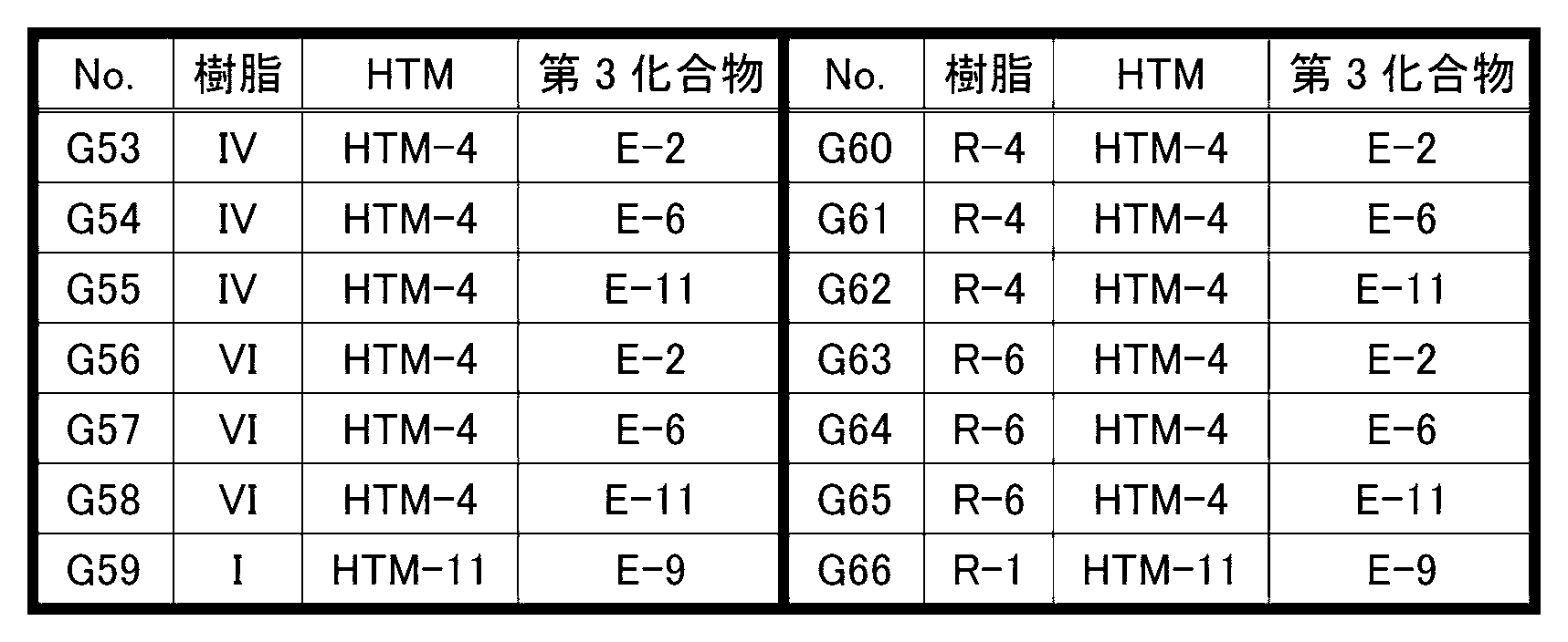
感光体の耐摩耗性を向上させ、形成画像におけるカブリの発生を抑制するためには、電荷輸送層が含有するポリアリレート樹脂、正孔輸送剤、及び第3化合物の組み合わせが、表2及び表3に示す組み合わせNo.G1~G66の各々であることが好ましい。同じ理由から、電荷輸送層が含有するポリアリレート樹脂、正孔輸送剤、及び第3化合物の組み合わせが、表2及び表3に示す組み合わせNo.G1~G66の各々であり、電荷発生層が含有する電荷発生剤がY型チタニルフタロシアニンであることがより好ましい。 In order to improve the wear resistance of the photoreceptor and suppress the occurrence of fogging in the formed image, the combination of the polyarylate resin, the hole transport agent, and the third compound contained in the charge transport layer should be selected as shown in Table 2 and Table 2. Combination No. 3 shown in FIG. Each of G1 to G66 is preferred. For the same reason, the combination of the polyarylate resin, the hole transport agent, and the third compound contained in the charge transport layer is the combination No. shown in Tables 2 and 3. Each of G1 to G66 and the charge generating agent contained in the charge generating layer is more preferably Y-type titanyl phthalocyanine.

上記表1~表3中の用語の意味は次の通りである。「No.」は「組み合わせNo.」を示す。「樹脂」は「ポリアリレート樹脂」を示す。「HTM」は「正孔輸送剤」を示す。 The meanings of the terms in Tables 1 to 3 are as follows. "No." indicates "combination No.". "Resin" means "polyarylate resin". "HTM" stands for "hole transport agent".
(導電性基体)
導電性基体は、感光体の導電性基体として用いることができる限り、特に限定されない。導電性基体は、少なくとも表面部が導電性を有する材料で構成されていればよい。導電性基体の一例としては、導電性を有する材料で構成される導電性基体が挙げられる。導電性基体の別の例としては、導電性を有する材料で被覆される導電性基体が挙げられる。導電性を有する材料としては、例えば、アルミニウム、鉄、銅、錫、白金、銀、バナジウム、モリブデン、クロム、カドミウム、チタン、ニッケル、パラジウム、インジウム、ステンレス鋼、及び真鍮が挙げられる。これらの導電性を有する材料を単独で用いてもよいし、2種以上を組み合わせて(例えば、合金として)用いてもよい。これらの導電性を有する材料のなかでも、感光層から導電性基体への電荷の移動が良好であることから、アルミニウム及びアルミニウム合金が好ましい。
(Conductive substrate)
The conductive substrate is not particularly limited as long as it can be used as the conductive substrate of the photoreceptor. At least the surface portion of the conductive substrate may be made of a conductive material. An example of the conductive substrate is a conductive substrate made of a conductive material. Another example of a conductive substrate is a conductive substrate coated with a material having electrical conductivity. Conductive materials include, for example, aluminum, iron, copper, tin, platinum, silver, vanadium, molybdenum, chromium, cadmium, titanium, nickel, palladium, indium, stainless steel, and brass. These conductive materials may be used alone, or two or more of them may be used in combination (for example, as an alloy). Among these electrically conductive materials, aluminum and aluminum alloys are preferred because of good charge transfer from the photosensitive layer to the conductive substrate.
導電性基体の形状は、画像形成装置の構造に合わせて適宜選択される。導電性基体の形状としては、例えば、シート状及びドラム状が挙げられる。また、導電性基体の厚さは、導電性基体の形状に応じて適宜選択される。 The shape of the conductive substrate is appropriately selected according to the structure of the image forming apparatus. Examples of the shape of the conductive substrate include a sheet shape and a drum shape. Moreover, the thickness of the conductive substrate is appropriately selected according to the shape of the conductive substrate.
(中間層)
中間層(下引き層)は、例えば、無機粒子及び中間層に用いられる樹脂(中間層用樹脂)を含有する。中間層が存在することにより、リーク発生を抑制し得る程度の絶縁状態を維持しつつ、感光体を露光した時に発生する電流の流れを円滑にして、抵抗の上昇を抑制できる。
(middle layer)
The intermediate layer (undercoat layer) contains, for example, inorganic particles and a resin used for the intermediate layer (intermediate layer resin). The presence of the intermediate layer makes it possible to maintain an insulating state to the extent that leakage can be suppressed, and to smooth the flow of current generated when the photosensitive member is exposed to light, thereby suppressing an increase in resistance.
無機粒子としては、例えば、金属(例えば、アルミニウム、鉄、及び銅)の粒子、金属酸化物(例えば、酸化チタン、アルミナ、酸化ジルコニウム、酸化スズ、及び酸化亜鉛)の粒子、及び非金属酸化物(例えば、シリカ)の粒子が挙げられる。これらの無機粒子は、1種を単独で用いてもよいし、2種以上を併用してもよい。 Examples of inorganic particles include particles of metals (e.g., aluminum, iron, and copper), particles of metal oxides (e.g., titanium oxide, alumina, zirconium oxide, tin oxide, and zinc oxide), and non-metal oxides. (eg, silica) particles. One of these inorganic particles may be used alone, or two or more thereof may be used in combination.
中間層用樹脂の例は、電荷輸送層に含有されるその他のバインダー樹脂の例と同じである。中間層は、添加剤を含有してもよい。中間層に含有される添加剤の例は、感光層に含有される添加剤の例と同じである。 Examples of the intermediate layer resin are the same as the other binder resins contained in the charge transport layer. The intermediate layer may contain additives. Examples of additives contained in the intermediate layer are the same as examples of additives contained in the photosensitive layer.
(感光体の製造方法)
感光体の製造方法の一例を説明する。感光体の製造方法は、電荷発生層形成工程と電荷輸送層形成工程とを含む。電荷発生層形成工程では、まず、電荷発生層を形成するための塗布液(以下、電荷発生層用塗布液と記載することがある)を調製する。電荷発生層用塗布液を導電性基体上に塗布する。次いで、塗布した電荷発生層用塗布液に含有される溶剤の少なくとも一部を除去して電荷発生層を形成する。電荷発生層用塗布液は、例えば、電荷発生剤と、ベース樹脂と、溶剤とを含有する。このような電荷発生層用塗布液は、電荷発生剤及びベース樹脂を、溶剤に溶解又は分散させることにより調製される。電荷発生層用塗布液は、必要に応じて、添加剤を更に含有してもよい。
(Manufacturing method of photoreceptor)
An example of a method for manufacturing a photoreceptor will be described. A photoreceptor manufacturing method includes a charge generating layer forming step and a charge transport layer forming step. In the charge generation layer forming step, first, a coating liquid for forming the charge generation layer (hereinafter sometimes referred to as a charge generation layer coating liquid) is prepared. A charge generation layer coating liquid is applied onto a conductive substrate. Next, at least part of the solvent contained in the applied charge-generating layer coating liquid is removed to form the charge-generating layer. The charge generating layer coating liquid contains, for example, a charge generating agent, a base resin, and a solvent. Such a charge generation layer coating liquid is prepared by dissolving or dispersing a charge generation agent and a base resin in a solvent. The charge generation layer coating liquid may further contain additives, if necessary.
電荷輸送層形成工程では、まず、電荷輸送層を形成するための塗布液(以下、電荷輸送層用塗布液と記載することがある)を調製する。電荷輸送層用塗布液を電荷発生層上に塗布する。次いで、塗布した電荷輸送層用塗布液に含有される溶剤の少なくとも一部を除去して電荷輸送層を形成する。電荷輸送層用塗布液は、正孔輸送剤と、バインダー樹脂と、溶剤とを含む。電荷輸送層用塗布液は、正孔輸送剤と、バインダー樹脂とを、溶剤に溶解又は分散させることにより調製できる。電荷輸送層用塗布液は、必要に応じて、第3化合物及び添加剤のうちの少なくとも1つを更に含有してもよい。 In the charge transport layer forming step, first, a coating liquid for forming the charge transport layer (hereinafter sometimes referred to as a charge transport layer coating liquid) is prepared. The charge transport layer coating liquid is applied onto the charge generation layer. Next, at least part of the solvent contained in the applied charge transport layer coating liquid is removed to form the charge transport layer. The charge transport layer coating liquid contains a hole transport agent, a binder resin, and a solvent. The charge transport layer coating liquid can be prepared by dissolving or dispersing a hole transport agent and a binder resin in a solvent. The charge transport layer coating liquid may further contain at least one of a third compound and an additive, if necessary.
電荷発生層用塗布液、及び電荷輸送層用塗布液(以下、これらを包括的に塗布液と記載することがある)に含有される溶剤は、塗布液に含有される各成分を溶解又は分散できる限り、特に限定されない。溶剤としては、例えば、アルコール(より具体的には、メタノール、エタノール、イソプロパノール、及びブタノール等)、脂肪族炭化水素(より具体的には、n-ヘキサン、オクタン、及びシクロヘキサン等)、芳香族炭化水素(より具体的には、ベンゼン、トルエン、及びキシレン等)、ハロゲン化炭化水素(より具体的には、ジクロロメタン、ジクロロエタン、四塩化炭素、及びクロロベンゼン等)、エーテル(より具体的には、ジメチルエーテル、ジエチルエーテル、テトラヒドロフラン、エチレングリコールジメチルエーテル、及びジエチレングリコールジメチルエーテル等)、ケトン(より具体的には、アセトン、メチルエチルケトン、及びシクロヘキサノン等)、エステル(より具体的には、酢酸エチル、及び酢酸メチル等)、ジメチルホルムアルデヒド、ジメチルホルムアミド、及びジメチルスルホキシドが挙げられる。これらの溶剤は、1種を単独で用いてもよいし、2種以上を組み合わせて用いてもよい。 The solvent contained in the charge-generating layer coating liquid and the charge-transporting layer coating liquid (hereinafter collectively referred to as the coating liquid in some cases) dissolves or disperses each component contained in the coating liquid. It is not particularly limited as long as possible. Examples of solvents include alcohols (more specifically, methanol, ethanol, isopropanol, butanol, etc.), aliphatic hydrocarbons (more specifically, n-hexane, octane, cyclohexane, etc.), aromatic hydrocarbons, etc. Hydrogen (more specifically, benzene, toluene, xylene, etc.), halogenated hydrocarbons (more specifically, dichloromethane, dichloroethane, carbon tetrachloride, chlorobenzene, etc.), ethers (more specifically, dimethyl ether , diethyl ether, tetrahydrofuran, ethylene glycol dimethyl ether, and diethylene glycol dimethyl ether), ketones (more specifically, acetone, methyl ethyl ketone, cyclohexanone, etc.), esters (more specifically, ethyl acetate, methyl acetate, etc.), Dimethylformaldehyde, dimethylformamide, and dimethylsulfoxide. These solvents may be used singly or in combination of two or more.
電荷輸送層用塗布液に含有される溶剤は、電荷発生層用塗布液に含有される溶剤と、異なることが好ましい。電荷発生層上に電荷輸送層用塗布液を塗布する場合に、電荷発生層が電荷輸送層用塗布液の溶剤に溶解しないことが好ましいからである。 The solvent contained in the charge-transporting layer coating liquid is preferably different from the solvent contained in the charge-generating layer coating liquid. This is because when the charge-transporting layer coating liquid is applied onto the charge-generating layer, it is preferable that the charge-generating layer does not dissolve in the solvent of the charge-transporting layer coating liquid.
塗布液は、それぞれ各成分を混合し、溶剤に分散することにより調製される。混合又は分散には、例えば、ビーズミル、ロールミル、ボールミル、アトライター、ペイントシェーカー、又は超音波分散器を用いることができる。 The coating liquid is prepared by mixing each component and dispersing it in a solvent. For mixing or dispersing, for example, a bead mill, roll mill, ball mill, attritor, paint shaker, or ultrasonic disperser can be used.
塗布液を塗布する方法は、塗布液を均一に塗布できる方法であれば、特に限定されない。塗布方法としては、例えば、ディップコート法、スプレーコート法、スピンコート法、及びバーコート法が挙げられる。 The method of applying the coating liquid is not particularly limited as long as the method can uniformly apply the coating liquid. Examples of coating methods include dip coating, spray coating, spin coating, and bar coating.
塗布液に含有される溶剤の少なくとも一部を除去する方法としては、例えば、加熱、減圧、又は加熱と減圧との併用が挙げられる。より具体的には、高温乾燥機、又は減圧乾燥機を用いて、熱処理(熱風乾燥)する方法が挙げられる。熱処理の温度は、例えば、40℃以上150℃以下である。熱処理の時間は、例えば、3分以上120分以下である。 Methods for removing at least part of the solvent contained in the coating liquid include, for example, heating, reduced pressure, or combined use of heating and reduced pressure. More specifically, a method of heat treatment (hot air drying) using a high-temperature dryer or a reduced-pressure dryer can be mentioned. The heat treatment temperature is, for example, 40° C. or higher and 150° C. or lower. The heat treatment time is, for example, 3 minutes or more and 120 minutes or less.
なお、感光体の製造方法は、必要に応じて中間層を形成する工程を更に含んでいてもよい。中間層を形成する工程は、公知の方法を適宜選択することができる。 Incidentally, the method for manufacturing a photoreceptor may further include a step of forming an intermediate layer, if necessary. A known method can be appropriately selected for the step of forming the intermediate layer.
以下、実施例を用いて本発明を更に具体的に説明する。しかし、本発明は実施例の範囲に何ら限定されない。 EXAMPLES Hereinafter, the present invention will be described more specifically using examples. However, the present invention is in no way limited to the scope of the examples.
<正孔輸送剤>
正孔輸送剤として、実施形態で述べた正孔輸送剤(HTM-1)~(HTM-11)を準備した。
<Hole transport agent>
As hole transport agents, the hole transport agents (HTM-1) to (HTM-11) described in the embodiment were prepared.
<比較例で使用する正孔輸送剤>
比較例で使用する正孔輸送剤として、正孔輸送剤(HTM-A)~(HTM-E)を準備した。正孔輸送剤(HTM-A)~(HTM-E)は、各々、下記化学式(HTM-A)~(HTM-E)で表される。
<Hole Transport Agent Used in Comparative Example>
As hole transport agents used in comparative examples, hole transport agents (HTM-A) to (HTM-E) were prepared. The hole transport agents (HTM-A) to (HTM-E) are represented by the following chemical formulas (HTM-A) to (HTM-E), respectively.


<第3化合物>
第3化合物として、実施形態で述べた第3化合物(E-1)~(E-11)を準備した。
<Third compound>
As the third compounds, the third compounds (E-1) to (E-11) described in the embodiment were prepared.
<ポリアリレート樹脂(R-1)~(R-6)>
実施形態で述べたポリアリレート樹脂(R-1)~(R-6)の各々を、以下の方法で合成した。
<Polyarylate Resins (R-1) to (R-6)>
Each of the polyarylate resins (R-1) to (R-6) described in the embodiments was synthesized by the following method.
(ポリアリレート樹脂(R-1)の合成)
反応容器として、温度計、三方コック、及び滴下ロートを備えた三口フラスコを用いた。反応容器に、化合物(BP-1-1)(30.9ミリモル)と、化合物(BP-2)(10.3ミリモル)と、p-tert-ブチルフェノール(0.413ミリモル)と、水酸化ナトリウム(98ミリモル)と、ベンジルトリブチルアンモニウムクロライド(0.384ミリモル)とを入れた。反応容器内の空気をアルゴンガスで置換した。反応容器の内容物に水(300mL)を加えた。反応容器の内容物を50℃で1時間攪拌した。反応容器の内容物の温度が10℃になるまで反応容器の内容物を冷却して、アルカリ性水溶液Aを得た。
(Synthesis of polyarylate resin (R-1))
A three-necked flask equipped with a thermometer, a three-way cock, and a dropping funnel was used as a reaction vessel. A reaction vessel was charged with compound (BP-1-1) (30.9 mmol), compound (BP-2) (10.3 mmol), p-tert-butylphenol (0.413 mmol), and sodium hydroxide. (98 mmol) and benzyltributylammonium chloride (0.384 mmol) were charged. The air in the reaction vessel was replaced with argon gas. Water (300 mL) was added to the contents of the reaction vessel. The contents of the reaction vessel were stirred at 50° C. for 1 hour. The contents of the reaction vessel were cooled until the temperature of the contents of the reaction vessel reached 10° C. to obtain an alkaline aqueous solution A.
次に、化合物(DC-3)のジカルボン酸ジクロライド(32.4ミリモル)を、クロロホルム(150mL)に溶解させた。これにより、クロロホルム溶液Bを得た。 Next, the compound (DC-3) dicarboxylic acid dichloride (32.4 mmol) was dissolved in chloroform (150 mL). A chloroform solution B was thus obtained.
アルカリ性水溶液Aに対して、滴下ロートを用いて、110分間かけてゆっくりとクロロホルム溶液Bを滴下した。反応容器の内容物の温度(液温)を15±5℃に調節しながら、反応容器の内容物を4時間攪拌して重合反応を進行させた。デカントを用いて反応容器の内容物の上層(水層)を除去し、有機層を得た。次いで、三角フラスコに、イオン交換水(400mL)を加えた。三角フラスコ内に、得られた有機層を更に加えた。三角フラスコ内に、クロロホルム(400mL)及び酢酸(2mL)を更に加えた。三角フラスコ内容物を、室温(25℃)で30分間攪拌した。デカントを用いて三角フラスコ内容物の上層(水層)を除去し、有機層を得た。分液ロートを用いて、イオン交換水(1L)で、得られた有機層を洗浄した。イオン交換水による洗浄を5回繰り返し、水洗した有機層を得た。次に、水洗した有機層をろ過し、ろ液を得た。メタノール(1L)に得られたろ液をゆっくりと滴下し、沈殿物を得た。沈殿物をろ過により取り出した。取り出した沈殿物を温度70℃で12時間真空乾燥させた。これにより、ポリアリレート樹脂(R-1)が得られた。 Using a dropping funnel, the chloroform solution B was slowly added dropwise to the alkaline aqueous solution A over 110 minutes. While adjusting the temperature (liquid temperature) of the contents of the reaction vessel to 15±5° C., the contents of the reaction vessel were stirred for 4 hours to allow the polymerization reaction to proceed. The upper layer (aqueous layer) of the contents of the reaction vessel was removed using decanting to obtain an organic layer. Then, ion-exchanged water (400 mL) was added to the Erlenmeyer flask. The resulting organic layer was further added to the Erlenmeyer flask. Chloroform (400 mL) and acetic acid (2 mL) were further added to the Erlenmeyer flask. The contents of the Erlenmeyer flask were stirred at room temperature (25° C.) for 30 minutes. The upper layer (aqueous layer) of the contents of the Erlenmeyer flask was removed using decanting to obtain an organic layer. Using a separating funnel, the obtained organic layer was washed with ion-exchanged water (1 L). Washing with ion-exchanged water was repeated five times to obtain a water-washed organic layer. Next, the organic layer washed with water was filtered to obtain a filtrate. The resulting filtrate was slowly added dropwise to methanol (1 L) to obtain a precipitate. The precipitate was removed by filtration. The sediment taken out was vacuum-dried at a temperature of 70° C. for 12 hours. Thus, a polyarylate resin (R-1) was obtained.
(ポリアリレート樹脂(R-2)の合成)
化合物(BP-1-1)(30.9ミリモル)を化合物(BP-1-5)(30.9ミリモル)に変更した以外は、ポリアリレート樹脂(R-1)の合成と同じ方法で、ポリアリレート樹脂(R-2)を得た。
(Synthesis of polyarylate resin (R-2))
In the same manner as in the synthesis of polyarylate resin (R-1), except that compound (BP-1-1) (30.9 mmol) was changed to compound (BP-1-5) (30.9 mmol), A polyarylate resin (R-2) was obtained.
(ポリアリレート樹脂(R-3)の合成)
化合物(BP-1-1)(30.9ミリモル)を化合物(BP-1-2)(30.9ミリモル)に変更した以外は、ポリアリレート樹脂(R-1)の合成と同じ方法で、ポリアリレート樹脂(R-3)を得た。
(Synthesis of polyarylate resin (R-3))
In the same manner as in the synthesis of the polyarylate resin (R-1), except that the compound (BP-1-1) (30.9 mmol) was changed to the compound (BP-1-2) (30.9 mmol), A polyarylate resin (R-3) was obtained.
(ポリアリレート樹脂(R-4)の合成)
化合物(BP-1-1)(30.9ミリモル)を化合物(BP-1-3)(30.9ミリモル)に変更した以外は、ポリアリレート樹脂(R-1)の合成と同じ方法で、ポリアリレート樹脂(R-4)を得た。
(Synthesis of polyarylate resin (R-4))
In the same manner as in the synthesis of the polyarylate resin (R-1), except that the compound (BP-1-1) (30.9 mmol) was changed to the compound (BP-1-3) (30.9 mmol), A polyarylate resin (R-4) was obtained.
(ポリアリレート樹脂(R-5)の合成)
化合物(BP-1-1)(30.9ミリモル)を化合物(BP-1-4)(30.9ミリモル)に変更した以外は、ポリアリレート樹脂(R-1)の合成と同じ方法で、ポリアリレート樹脂(R-5)を得た。
(Synthesis of polyarylate resin (R-5))
In the same manner as in the synthesis of the polyarylate resin (R-1), except that the compound (BP-1-1) (30.9 mmol) was changed to the compound (BP-1-4) (30.9 mmol), A polyarylate resin (R-5) was obtained.
(ポリアリレート樹脂(R-6)の合成)
化合物(BP-1-1)(30.9ミリモル)及び化合物(BP-2)(10.3ミリモル)を、化合物(BP-1-1)(20.6ミリモル)及び化合物(BP-2)(20.6ミリモル)に変更した以外は、ポリアリレート樹脂(R-1)の合成と同じ方法で、ポリアリレート樹脂(R-6)を得た。
(Synthesis of polyarylate resin (R-6))
Compound (BP-1-1) (30.9 mmol) and compound (BP-2) (10.3 mmol), compound (BP-1-1) (20.6 mmol) and compound (BP-2) A polyarylate resin (R-6) was obtained in the same manner as the synthesis of the polyarylate resin (R-1), except that it was changed to (20.6 mmol).
得られたポリアリレート樹脂(R-1)、(R-2)、(R-3)、(R-4)、(R-5)、及び(R-6)の粘度平均分子量は、各々、50500、51,000、45,000、47,300、45,500、及び48,700であった。 The viscosity average molecular weights of the obtained polyarylate resins (R-1), (R-2), (R-3), (R-4), (R-5), and (R-6) are, respectively, 50,500, 51,000, 45,000, 47,300, 45,500 and 48,700.
プロトン核磁気共鳴分光計(日本分光株式会社製、300MHz)を用いて、得られたポリアリレート樹脂(R-1)~(R-6)の1H-NMRスペクトルを測定した。溶媒としてCDCl3を用いた。内部標準試料としてテトラメチルシラン(TMS)を用いた。ポリアリレート樹脂(R-1)~(R-6)のうちの代表例として、ポリアリレート樹脂(R-6)の化学シフト値を以下に示す。化学シフト値から、ポリアリレート樹脂(R-6)が得られていることを確認した。ポリアリレート樹脂(R-1)~(R-5)についても同じ方法で、ポリアリレート樹脂(R-1)~(R-5)が各々得られていることを確認した。 Using a proton nuclear magnetic resonance spectrometer (manufactured by JASCO Corporation, 300 MHz), 1 H-NMR spectra of the obtained polyarylate resins (R-1) to (R-6) were measured. CDCl 3 was used as solvent. Tetramethylsilane (TMS) was used as an internal standard sample. As a representative example of polyarylate resins (R-1) to (R-6), the chemical shift value of polyarylate resin (R-6) is shown below. It was confirmed from the chemical shift value that a polyarylate resin (R-6) was obtained. Polyarylate resins (R-1) to (R-5) were confirmed by the same method to be obtained respectively.
ポリアリレート樹脂(R-6):1H-NMR(300MHz,CDCl3)δ=8.21-8.26(m,8H), 7.25-7.29(m,4H), 7.07-7.23(m,20H), 2.16(q,2H), 1.65(s,3H), 0.78(t,3H). Polyarylate resin (R-6): 1 H-NMR (300 MHz, CDCl 3 ) δ = 8.21-8.26 (m, 8H), 7.25-7.29 (m, 4H), 7.07 -7.23 (m, 20H), 2.16 (q, 2H), 1.65 (s, 3H), 0.78 (t, 3H).
<比較例で使用するポリアリレート樹脂の準備>
また、比較例で使用するポリアリレート樹脂として、ポリアリレート樹脂(R-A)~(R-D)の各々を準備した。ポリアリレート樹脂(R-A)~(R-C)の各々は、下記化学式(R-A)~(R-C)で表される。なお、各繰り返し単位の右下に付された数字は、ポリアリレート樹脂に含まれる繰り返し単位の総数に対する、各繰り返し単位の数の百分率(%)を示す。
<Preparation of polyarylate resin used in Comparative Example>
Further, polyarylate resins (RA) to (RD) were prepared as polyarylate resins used in comparative examples. Each of the polyarylate resins (RA) to (RC) is represented by the following chemical formulas (RA) to (RC). The number attached to the lower right of each repeating unit indicates the percentage (%) of the number of each repeating unit with respect to the total number of repeating units contained in the polyarylate resin.

ポリアリレート樹脂(R-D)は、ビスフェノール由来繰り返し単位として、下記繰り返し単位(BP-A)及び(BP-C)のみを含む。ポリアリレート樹脂(R-D)は、ジカルボン酸由来繰り返し単位として、下記繰り返し単位(3)、(DC-T)及び(DC-I)のみを含む。ポリアリレート樹脂(R-D)に含まれる繰り返し単位の総数に対する、繰り返し単位(BP-A)の数の百分率、繰り返し単位(BP-C)の数の百分率、繰り返し単位(3)の数の百分率、繰り返し単位(DC-T)の数の百分率、及び繰り返し単位(DC-I)の数の百分率は、各々、25.0%、25.0%、25.0%、15.0%、及び10.0%である。 The polyarylate resin (RD) contains only the following repeating units (BP-A) and (BP-C) as bisphenol-derived repeating units. The polyarylate resin (RD) contains only the following repeating units (3), (DC-T) and (DC-I) as dicarboxylic acid-derived repeating units. Percentage of the number of repeating units (BP-A), percentage of the number of repeating units (BP-C), percentage of the number of repeating units (3) with respect to the total number of repeating units contained in the polyarylate resin (RD) , the percentage of the number of repeating units (DC-T), and the percentage of the number of repeating units (DC-I) are respectively 25.0%, 25.0%, 25.0%, 15.0%, and 10.0%.

なお、ポリアリレート樹脂(R-A)、(R-B)、(R-C)、及び(R-D)の粘度平均分子量は、各々、45,300、51,000、46,700、及び46,800であった。 The viscosity average molecular weights of the polyarylate resins (RA), (RB), (RC), and (RD) are 45,300, 51,000, 46,700, and 46,800.
<各ポリアリレート樹脂の構成>
上記各ポリアリレート樹脂の構成を、表4に示す。詳しくは、ポリアリレート樹脂(R-1)~(R-6)及び(R-A)~(R-D)のビスフェノール由来繰り返し単位の種類、比率n1/n2、及びジカルボン酸由来繰り返し単位の種類を、表4に示す。表4中の「-」は該当する値がないことを示す。
<Structure of each polyarylate resin>
Table 4 shows the composition of each polyarylate resin. Specifically, the types of bisphenol-derived repeating units of polyarylate resins (R-1) to (R-6) and (RA) to (RD), ratios n 1 /n 2 , and dicarboxylic acid-derived repeating units The types of are shown in Table 4. "-" in Table 4 indicates that there is no applicable value.

<感光体の製造>
次に、以下の方法により、感光体(A-1)~(A-28)及び(B-1)~(B-11)を製造した。
<Production of Photoreceptor>
Next, photoconductors (A-1) to (A-28) and (B-1) to (B-11) were produced by the following method.
(感光体(A-1)の製造)
まず、中間層を形成した。表面処理された酸化チタン(テイカ株式会社製「試作品SMT-A」、数平均一次粒子径10nm)を準備した。SMT-Aは、アルミナとシリカとを用いて酸化チタンを表面処理し、表面処理された酸化チタンを湿式分散しながらメチルハイドロジェンポリシロキサンを用いて更に表面処理したものであった。次いで、SMT-Aの2質量部と、ポリアミド樹脂(東レ株式会社製「アミラン(登録商標)CM8000」、ポリアミド6、ポリアミド12、ポリアミド66及びポリアミド610の四元共重合ポリアミド樹脂)1質量部と、メタノール10質量部と、ブタノール1質量部と、トルエン1質量部とを、ビーズミルを用いて5時間混合して、中間層用塗布液を得た。中間層用塗布液を、目開き5μmのフィルターを用いてろ過した。その後、ディップコート法により、導電性基体の表面に中間層用塗布液を塗布した。導電性基体としては、アルミニウム製のドラム状支持体を用いた。続いて、塗布した中間層用塗布液を130℃で30分間乾燥させて、導電性基体上に中間層(膜厚1.5μm)を形成した。
(Production of photoreceptor (A-1))
First, an intermediate layer was formed. A surface-treated titanium oxide (“Prototype SMT-A” manufactured by Tayca Co., Ltd., number average primary particle diameter 10 nm) was prepared. SMT-A was obtained by surface-treating titanium oxide with alumina and silica, and further surface-treating it with methylhydrogenpolysiloxane while dispersing the surface-treated titanium oxide in a wet process. Next, 2 parts by mass of SMT-A, and 1 part by mass of a polyamide resin (“Amilan (registered trademark) CM8000” manufactured by Toray Industries, Inc., a quaternary copolymerized polyamide resin of polyamide 6, polyamide 12, polyamide 66 and polyamide 610) , 10 parts by mass of methanol, 1 part by mass of butanol, and 1 part by mass of toluene were mixed for 5 hours using a bead mill to obtain an intermediate layer coating liquid. The intermediate layer coating liquid was filtered using a filter with an opening of 5 μm. Thereafter, the intermediate layer coating liquid was applied to the surface of the conductive substrate by a dip coating method. A drum-like support made of aluminum was used as the conductive substrate. Subsequently, the applied intermediate layer coating liquid was dried at 130° C. for 30 minutes to form an intermediate layer (thickness: 1.5 μm) on the conductive substrate.
次に、電荷発生層を形成した。詳しくは、電荷発生剤であるY型チタニルフタロシアニン1.5質量部と、ベース樹脂であるポリビニルアセタール樹脂(積水化学工業株式会社製「エスレックBX-5」)1.0質量部と、プロピレングリコールモノメチルエーテル40.0質量部と、テトラヒドロフラン40.0質量部とを、ビーズミルを用いて12時間混合して、電荷発生層用塗布液を得た。電荷発生層用塗布液を、目開き3μmのフィルターを用いてろ過した。ディップコート法により、得られたろ液を中間層上に塗布し、50℃で5分間乾燥させた。このようにして、中間層上に電荷発生層(膜厚0.3μm)を形成した。 Next, a charge generation layer was formed. Specifically, 1.5 parts by mass of Y-type titanyl phthalocyanine as a charge generating agent, 1.0 parts by mass of polyvinyl acetal resin (“S-Lec BX-5” manufactured by Sekisui Chemical Co., Ltd.) as a base resin, and 1.0 part by mass of propylene glycol monomethyl 40.0 parts by mass of ether and 40.0 parts by mass of tetrahydrofuran were mixed for 12 hours using a bead mill to obtain a charge generation layer coating liquid. The charge generation layer coating liquid was filtered using a filter with an opening of 3 μm. The resulting filtrate was applied onto the intermediate layer by dip coating and dried at 50° C. for 5 minutes. Thus, a charge generating layer (thickness: 0.3 μm) was formed on the intermediate layer.
次に、電荷輸送層を形成した。詳しくは、正孔輸送剤(HTM-1)45質量部と、バインダー樹脂であるポリアリレート樹脂(R-1)100質量部と、第3化合物(E-1)2質量部と、テトラヒドロフラン550質量部と、トルエン150質量部とを混合して、電荷輸送層用塗布液を得た。ディップコート法により、電荷輸送層用塗布液を電荷発生層上に塗布し、120℃で40分間乾燥させた。このようにして、電荷発生層上に電荷輸送層(膜厚20μm)を形成し、感光体(A-1)を得た。感光体(A-1)において、導電性基体上に中間層が、中間層上に電荷発生層が、電荷発生層上に電荷輸送層が備えられていた。 Next, a charge transport layer was formed. Specifically, 45 parts by mass of a hole transport agent (HTM-1), 100 parts by mass of a polyarylate resin (R-1) as a binder resin, 2 parts by mass of a third compound (E-1), and 550 parts by mass of tetrahydrofuran parts and 150 parts by mass of toluene were mixed to obtain a charge transport layer coating liquid. The charge transport layer coating liquid was applied onto the charge generation layer by dip coating and dried at 120° C. for 40 minutes. Thus, a charge transport layer (thickness: 20 μm) was formed on the charge generation layer to obtain a photoreceptor (A-1). Photoreceptor (A-1) had an intermediate layer on the conductive substrate, a charge generation layer on the intermediate layer, and a charge transport layer on the charge generation layer.
(感光体(A-2)~(A-11)、(A-14)~(A-28)、(B-1)~(B-4)、及び(B-7)~(B-11)の製造)
表5~表7に示すポリアリレート樹脂、正孔輸送剤、及び第3化合物を使用したこと以外は、感光体(A-1)の製造と同じ方法で、感光体(A-2)~(A-11)、(A-14)~(A-28)、(B-1)~(B-4)、及び(B-7)~(B-11)の各々を製造した。
(Photoreceptors (A-2) to (A-11), (A-14) to (A-28), (B-1) to (B-4), and (B-7) to (B-11 )Manufacturing of)
Photoreceptors (A-2) to ( A-11), (A-14) to (A-28), (B-1) to (B-4), and (B-7) to (B-11) were each produced.
(感光体(A-12)~(A-13)、及び(B-5)~(B-6)の製造)
正孔輸送剤(HTM-1)の添加量を、表5及び表7に示す量に変更したこと以外は、感光体(A-1)の製造と同じ方法で、感光体(A-12)~(A-13)、及び(B-5)~(B-6)の各々を製造した。
(Production of photoreceptors (A-12) to (A-13) and (B-5) to (B-6))
Photoreceptor (A-12) was produced in the same manner as photoreceptor (A-1) except that the amount of hole transport agent (HTM-1) added was changed to the amount shown in Tables 5 and 7. ~ (A-13), and (B-5) ~ (B-6) were each produced.
<評価>
以下に示す方法で、評価対象の感光体である上記感光体(A-1)~(A-28)及び(B-1)~(B-11)の各々を評価した。
<Evaluation>
Each of the photoreceptors (A-1) to (A-28) and (B-1) to (B-11), which are photoreceptors to be evaluated, were evaluated by the following methods.
<トナーの摩擦帯電性の評価>
感光体の感光層(より具体的には、電荷輸送層)と摩擦されたときのトナーの摩擦帯電量を、次に示す方法で測定した。トナーの摩擦帯電量の測定には、治具(京セラドキュメントソリューションズ株式会社製)を用いた。
<Evaluation of triboelectrification property of toner>
The triboelectrification amount of the toner when rubbed with the photosensitive layer (more specifically, the charge transport layer) of the photoreceptor was measured by the following method. A jig (manufactured by Kyocera Document Solutions Co., Ltd.) was used to measure the triboelectric charge amount of the toner.
まず、第1フィルム及び第2フィルムとして、直径4cmの円形状のオーバーヘッドプロジェクタ(OHP)フィルムを準備した。第1フィルム及び第2フィルムの各々の上に、感光体(A-1)の製造に使用した電荷輸送層用塗布液を塗布した。塗布した電荷輸送層用塗布液を、120℃で40分間熱風乾燥させた。このようにして、電荷輸送層(膜厚20μm)を備える第1フィルム、及び電荷輸送層(膜厚20μm)を備える第2フィルムを得た。第1フィルムに備えられた電荷輸送層上に、カラープリンター用トナー(株式会社沖データ製「C542dnw」用マゼンタトナー、平均粒径:10μm)0.1gを載せた。トナーの上に、第2フィルムに備えられた電荷輸送層を載せた。このようにして、下から順に、第1フィルム、電荷輸送層、トナー、電荷輸送層、及び第2フィルムを配置した。温度50℃且つ相対湿度50%RHの環境下で、治具を用いて、第2フィルムに備えられた電荷輸送層を固定したまま、回転速度60rpmで1分間、第1フィルムに備えられた電荷輸送層を回転させた。これにより、2枚の電荷輸送層の間でトナーが摩擦され、トナーが摩擦帯電した。摩擦帯電したトナーを治具から取出し、帯電量測定装置(吸引式小型帯電量測定装置、トレック社製「MODEL 212HS」)を用いて吸引した。吸引されたトナーの総電気量Q(単位:+μC)と質量M(単位:g)とを、帯電量測定装置を用いて測定した。式「摩擦帯電量=Q/M」から、トナーの摩擦帯電量(単位:μC/g)を求めた。次いで、感光体(A-1)の製造に使用した電荷輸送層用塗布液を、感光体(A-2)~(A-28)及び(B-1)~(B-11)の各々の製造に使用した電荷輸送層用塗布液に変更したこと以外は、感光体(A-1)に対するトナーの摩擦帯電量の測定と同じ方法で、感光体(A-2)~(A-28)及び(B-1)~(B-11)に対するトナーの摩擦帯電量を測定した。測定されたトナーの摩擦帯電量を、表5~表7に示す。トナーの摩擦帯電量から、下記基準に従って、トナーの摩擦帯電性を評価した。
[トナーの摩擦帯電性の評価基準]
良好:トナーの摩擦帯電量が-20.0μC/g以下である。
不良:トナーの摩擦帯電量が-20.0μC/g超である。
First, circular overhead projector (OHP) films with a diameter of 4 cm were prepared as the first film and the second film. The charge transport layer coating solution used in the production of the photoreceptor (A-1) was applied onto each of the first film and the second film. The applied charge transport layer coating liquid was dried with hot air at 120° C. for 40 minutes. Thus, a first film having a charge transport layer (thickness of 20 μm) and a second film having a charge transport layer (thickness of 20 μm) were obtained. 0.1 g of toner for color printer (magenta toner for “C542dnw” manufactured by Oki Data Co., Ltd., average particle size: 10 μm) was placed on the charge transport layer provided on the first film. A charge transport layer provided in a second film was placed on top of the toner. Thus, the first film, the charge transport layer, the toner, the charge transport layer, and the second film were arranged in order from the bottom. In an environment of a temperature of 50° C. and a relative humidity of 50% RH, using a jig, while fixing the charge transport layer provided on the second film, the charge provided on the first film was rotated at a rotation speed of 60 rpm for 1 minute. The transport layer was rotated. This rubbed the toner between the two charge transport layers and triboelectrically charged the toner. The triboelectrically charged toner was taken out from the jig and sucked using a charge amount measuring device (suction type compact charge amount measuring device, "MODEL 212HS" manufactured by Trek). The total amount of electricity Q (unit: +μC) and the mass M (unit: g) of the attracted toner were measured using a charge amount measuring device. The triboelectrification amount (unit: μC/g) of the toner was obtained from the formula "amount of triboelectrification=Q/M". Next, the charge transport layer coating solution used in the production of the photoreceptor (A-1) was applied to each of the photoreceptors (A-2) to (A-28) and (B-1) to (B-11). Photoreceptors (A-2) to (A-28) were measured in the same manner as the measurement of the triboelectric charge amount of the toner for the photoreceptor (A-1), except that the coating liquid for the charge transport layer used in the production was changed. and (B-1) to (B-11) were measured. Tables 5 to 7 show the measured triboelectric charge amounts of the toner. Based on the triboelectrification amount of the toner, the triboelectrification property of the toner was evaluated according to the following criteria.
[Evaluation Criteria for Triboelectrification of Toner]
Good: The triboelectrification amount of the toner is -20.0 μC/g or less.
Poor: The amount of triboelectrification of the toner exceeds -20.0 μC/g.
<耐摩耗性の評価>
耐摩耗性の評価に使用した評価機は、カラープリンター(株式会社沖データ製「C542dnw」)であった。評価機のトナーカートリッジにシアントナーを充填した。まず、感光体の感光層(より具体的には、電荷輸送層)の膜厚T1を測定した。次いで、感光体を評価機に搭載した。次いで、温度23℃及び相対湿度50%RHの環境下で、評価機を用いて、300,000枚の用紙に、画像I(印字率1%のパターン画像)を印刷した。300,000枚の印刷後に、感光体の感光層の膜厚T2を測定した。そして、印刷前後の感光層の膜厚変化量である摩耗量(T1-T2、単位:μm)を求めた。摩耗量を、表5~表7に示す。求めた摩耗量から、下記基準に従って、感光体の耐摩耗性を評価した。
[耐摩耗性の評価基準]
良好:摩耗量が3.0μm以下である。
不良:摩耗量が3.0μm超である。
<Abrasion resistance evaluation>
A color printer (“C542dnw” manufactured by Oki Data Co., Ltd.) was used as an evaluation machine for evaluating abrasion resistance. Cyan toner was filled in the toner cartridge of the evaluation machine. First, the film thickness T1 of the photosensitive layer (more specifically, the charge transport layer) of the photoreceptor was measured. The photoreceptor was then mounted on the evaluation machine. Next, under an environment of a temperature of 23° C. and a relative humidity of 50% RH, an image I (pattern image with a print rate of 1%) was printed on 300,000 sheets of paper using the evaluation machine. After printing 300,000 sheets, the film thickness T2 of the photosensitive layer of the photoreceptor was measured. Then, the amount of wear (T1-T2, unit: μm), which is the change in thickness of the photosensitive layer before and after printing, was determined. The amount of wear is shown in Tables 5-7. The wear resistance of the photoreceptor was evaluated according to the following criteria from the obtained wear amount.
[Abrasion resistance evaluation criteria]
Good: Wear amount is 3.0 μm or less.
Poor: The amount of wear exceeds 3.0 μm.
<カブリ抑制の評価>
上記<耐摩耗性の評価>が完了した後、評価機を、高温高湿環境(温度32.5℃及び相対湿度85%)に移動させた。なお、この評価機は反転現像方式であり、帯電装置が感光体を負極性に帯電し、負帯電したトナーによって静電潜像が現像される構成であった。高温高湿環境下で、評価機を用いて、1枚の用紙に、画像II(白紙画像)を印刷した。反射濃度計(X-Rite社製「RD914」)を用いて、印刷した用紙の白紙画像部の反射濃度Aと、印刷を行っていない用紙の反射濃度Bとを測定した。そして、式「FD=反射濃度A-反射濃度B」に基づいて、カブリ濃度(FD)を求めた。求めたFDから、下記基準に従って、形成画像におけるカブリの発生が抑制されているかを評価した。評価結果を、表5~表7に示す。
<Evaluation of Fog Suppression>
After completing the above <evaluation of wear resistance>, the evaluation machine was moved to a high-temperature and high-humidity environment (temperature of 32.5°C and relative humidity of 85%). This evaluation machine was of a reversal development system, in which the charging device negatively charged the photoreceptor, and the electrostatic latent image was developed with the negatively charged toner. Image II (blank paper image) was printed on one sheet of paper using the evaluation machine under a high-temperature and high-humidity environment. Using a reflection densitometer ("RD914" manufactured by X-Rite), the reflection density A of the blank image area of the printed paper and the reflection density B of the unprinted paper were measured. Then, the fog density (FD) was obtained based on the formula "FD=reflection density A-reflection density B". Based on the obtained FD, it was evaluated whether or not the occurrence of fogging in the formed image was suppressed according to the following criteria. Evaluation results are shown in Tables 5 to 7.
[カブリ抑制の評価基準]
評価A(良好):FDが0.0%以上0.5%未満である。
評価B(やや不良):FDが0.5%以上2.5%未満である。
評価C(不良):FDが2.5%以上である。
[Evaluation Criteria for Suppression of Fog]
Evaluation A (good): FD is 0.0% or more and less than 0.5%.
Evaluation B (slightly poor): FD is 0.5% or more and less than 2.5%.
Evaluation C (poor): FD is 2.5% or more.
<電気特性の評価>
電気特性の評価は、温度10℃及び相対湿度20%RHの環境下で行った。ドラム感度試験機(ジェンテック株式会社製)を用いて、感光体の表面を-600Vに帯電させた。次いで、バンドパスフィルターを用いて、ハロゲンランプの白色光から単色光(波長780nm、光エネルギー0.8μJ/cm2)を取り出した。取り出された単色光を、感光体の表面に照射した。照射開始から80ミリ秒経過した時の感光体の表面電位を測定した。測定された表面電位を、露光後電位(VL、単位:V)とした。露光後電位を、表5~表7に示す。測定された露光後電位から、下記基準に従って、感光体の電気特性を評価した。
<Evaluation of electrical properties>
Evaluation of electrical properties was performed under an environment of a temperature of 10° C. and a relative humidity of 20% RH. The surface of the photoreceptor was charged to −600 V using a drum sensitivity tester (manufactured by Gentec Co., Ltd.). Then, a bandpass filter was used to extract monochromatic light (wavelength 780 nm, light energy 0.8 μJ/cm 2 ) from the white light of the halogen lamp. The surface of the photoreceptor was irradiated with the extracted monochromatic light. The surface potential of the photoreceptor was measured 80 milliseconds after the start of irradiation. The measured surface potential was taken as post-exposure potential (V L , unit: V). The post-exposure potentials are shown in Tables 5-7. From the measured post-exposure potential, the electrical properties of the photoreceptor were evaluated according to the following criteria.
[電気特性の評価基準]
良好:初期の感光体の露光後電位(VL)の絶対値が、100V以下である。
不良:初期の感光体の露光後電位(VL)の絶対値が、100V超である。
[Evaluation criteria for electrical characteristics]
Good: The absolute value of the initial post-exposure potential (V L ) of the photosensitive member is 100 V or less.
Poor: The absolute value of the post-exposure potential (V L ) of the initial photoreceptor is over 100V.
表5~表7中の用語は、次のとおりである。「樹脂」はポリアリレート樹脂を示す。「HTM」は、正孔輸送剤を示す。「量」は、100質量部のバインダー樹脂に対する正孔輸送剤の含有量を示す。「部」は、質量部を示す。「トナー摩擦帯電量」は、感光体の感光層と摩擦されたときのトナーの摩擦帯電量を示す。「FD」は、形成画像におけるカブリ抑制の評価結果を示す。「溶解せず」は、電荷輸送層用塗布液の調製時に、バインダー樹脂が溶剤に溶解せず、電荷輸送層が形成できなかったことを示す。 Terms in Tables 5 to 7 are as follows. "Resin" refers to polyarylate resin. "HTM" indicates hole transport agent. "Amount" indicates the content of the hole transport agent with respect to 100 parts by mass of the binder resin. "Parts" indicates parts by mass. The "toner triboelectric charge amount" indicates the triboelectric charge amount of the toner when rubbed against the photosensitive layer of the photoreceptor. "FD" indicates the evaluation result of fog suppression in the formed image. "Not dissolved" indicates that the binder resin was not dissolved in the solvent during the preparation of the charge transport layer coating liquid, and the charge transport layer could not be formed.


感光体(A-1)~(A-28)の電荷発生層は、電荷発生剤を含有していた。表5及び表6に示すように、感光体(A-1)~(A-28)の電荷輸送層は、正孔輸送剤と、バインダー樹脂(より具体的には、ポリアリレート樹脂(R-1)~(R-6)の何れか)とを少なくとも含有していた。表4に示すように、ポリアリレート樹脂(R-1)~(R-6)は、各々、繰り返し単位(1)と、繰り返し単位(2)と、繰り返し単位(3)とを含み、繰り返し単位(2)の数n2に対する繰り返し単位(1)の数n1の比率n1/n2が1.0以上であった。表5及び表6に示すように、正孔輸送剤は、一般式(21)、一般式(22)、一般式(23)、化学式(HTM-10)、又は一般式(24)に包含される、正孔輸送剤(HTM-1)~(HTM-11)のうちの1つであった。正孔輸送剤の含有量は、100質量部のバインダー樹脂に対して、30質量部以上45質量部以下であった。
The charge generation layers of photoreceptors (A-1) to (A-28) contained a charge generation agent. As shown in Tables 5 and 6, the charge transport layers of photoreceptors (A-1) to (A-28) consisted of a hole transport agent and a binder resin (more specifically, a polyarylate resin (R- 1) to (R-6)) at least. As shown in Table 4, polyarylate resins (R-1) to (R-6) each contain repeating unit (1), repeating unit (2), and repeating unit (3). The ratio n 1 / n 2 of the number n 1 of repeating units (1) to the
表5及び表6に示すように、感光体(A-1)~(A-28)の摩耗量は、3.0μm以下であり、これらの感光体は耐摩耗性に優れていた。 As shown in Tables 5 and 6, the photoreceptors (A-1) to (A-28) had an abrasion loss of 3.0 μm or less, and these photoreceptors were excellent in abrasion resistance.
表5及び表6に示すように、感光体(A-1)~(A-28)の電荷輸送層と摩擦されたときのトナーの摩擦帯電量は、-20.0μC/g以下であった。感光体(A-1)~(A-28)を用いて画像を形成した場合、カブリ抑制の評価結果はAであった。これらのことから示されるように、感光体(A-1)~(A-28)の電荷輸送層にトナーが接触した場合に、所望値以下の値に良好にトナーが負帯電するため、これらの感光体は形成画像におけるカブリの発生を抑制できていた。 As shown in Tables 5 and 6, the triboelectrification amount of the toner when rubbed against the charge transport layer of the photoreceptors (A-1) to (A-28) was -20.0 μC/g or less. . When images were formed using photoreceptors (A-1) to (A-28), the evaluation result of anti-fogging was A. As shown by these facts, when the toner comes into contact with the charge transport layers of the photoreceptors (A-1) to (A-28), the toner is satisfactorily negatively charged to a desired value or less. was able to suppress the occurrence of fogging in the formed image.
表5及び表6に示すように、感光体(A-1)~(A-28)の露光後電位の絶対値は100V以下であり、これらの感光体は、電気特性を維持しつつ、耐摩耗性に優れ、形成画像におけるカブリの発生を抑制できることが示された。 As shown in Tables 5 and 6, the absolute value of the post-exposure potential of the photoreceptors (A-1) to (A-28) was 100 V or less, and these photoreceptors maintained their electrical properties and their durability. It was shown that the abrasion resistance is excellent and the occurrence of fogging in the formed image can be suppressed.
以上のことから、本発明に係る感光体は、耐摩耗性に優れ、形成画像におけるカブリの発生を抑制できることが示された。 From the above, it was shown that the photoreceptor according to the present invention is excellent in wear resistance and can suppress the occurrence of fogging in formed images.
本発明に係る感光体は、画像形成装置に利用できる。 A photoreceptor according to the present invention can be used in an image forming apparatus.
1 :感光体(電子写真感光体)
2 :導電性基体
3 :感光層
3a :電荷発生層
3b :電荷輸送層
1: photoreceptor (electrophotographic photoreceptor)
2: Conductive substrate 3:
Claims (8)
前記感光層は、電荷発生層と、電荷輸送層とを含み、
前記電荷発生層は、電荷発生剤を含有し、
前記電荷輸送層は、正孔輸送剤とバインダー樹脂とを少なくとも含有し、
前記バインダー樹脂は、ポリアリレート樹脂を含み、前記ポリアリレート樹脂は、一般式(1)で表される繰り返し単位と、化学式(2)で表される繰り返し単位と、化学式(3)で表される繰り返し単位とを含み、前記化学式(2)で表される繰り返し単位の数n2に対する、前記一般式(1)で表される繰り返し単位の数n1の比率n1/n2は、1.0以上であり、
前記正孔輸送剤は、一般式(21)、一般式(22)、一般式(23)、化学式(HTM-10)、又は一般式(24)で表される化合物を含み、
前記正孔輸送剤の含有量は、100質量部の前記バインダー樹脂に対して、30質量部以上45質量部以下である、電子写真感光体。

R1及びR2は各々独立に水素原子又はメチル基を表し、R3はメチル基を表し、R4は水素原子、又は炭素原子数2若しくは3のアルキル基を表すか、或いは、
R1及びR2は各々メチル基を表し、R3及びR4は互いに結合して炭素原子数5又は6のシクロアルキリデン基を表す。)


前記一般式(22)中、R21、R22、及びR23は、各々独立に、炭素原子数1以上8以下のアルキル基、フェニル基、又は炭素原子数1以上8以下のアルコキシ基を表し、d1、d2、及びd3は、各々独立に、0以上5以下の整数を表し、
前記一般式(23)中、R31、R32、R33、及びR34は、各々独立に、炭素原子数1以上8以下のアルキル基、又は炭素原子数1以上8以下のアルコキシ基を表し、R35、及びR36は、各々独立に、水素原子、炭素原子数1以上8以下のアルキル基、又は炭素原子数6以上14以下のアリール基を表し、e1、e2、e3、及びe4は、各々独立に、0以上5以下の整数を表し、
前記一般式(24)中、R41、R42、R43、及びR44は、各々独立に、炭素原子数1以上8以下のアルキル基、又は炭素原子数1以上8以下のアルコキシ基を表し、f1、f2、f3、及びf4は、各々独立に、0以上5以下の整数を表す。) comprising a conductive substrate and a photosensitive layer;
The photosensitive layer includes a charge generation layer and a charge transport layer,
The charge generation layer contains a charge generation agent,
The charge transport layer contains at least a hole transport agent and a binder resin,
The binder resin includes a polyarylate resin, and the polyarylate resin includes repeating units represented by general formula (1), repeating units represented by chemical formula (2), and chemical formula (3). The ratio n 1 /n 2 of the number n 1 of repeating units represented by the general formula (1) to the number n 2 of repeating units represented by the chemical formula (2) is 1. is 0 or more,
The hole transport agent includes a compound represented by general formula (21), general formula (22), general formula (23), chemical formula (HTM-10), or general formula (24),
An electrophotographic photoreceptor, wherein the content of the hole transport agent is 30 parts by mass or more and 45 parts by mass or less with respect to 100 parts by mass of the binder resin.
R 1 and R 2 each independently represent a hydrogen atom or a methyl group, R 3 represents a methyl group, and R 4 represents a hydrogen atom or an alkyl group having 2 or 3 carbon atoms, or
R 1 and R 2 each represent a methyl group, and R 3 and R 4 are combined to represent a cycloalkylidene group having 5 or 6 carbon atoms. )
In general formula (22), R 21 , R 22 , and R 23 each independently represent an alkyl group having 1 to 8 carbon atoms, a phenyl group, or an alkoxy group having 1 to 8 carbon atoms. , d1, d2, and d3 each independently represent an integer of 0 to 5,
In general formula (23), R 31 , R 32 , R 33 and R 34 each independently represent an alkyl group having 1 to 8 carbon atoms or an alkoxy group having 1 to 8 carbon atoms. , R 35 , and R 36 each independently represent a hydrogen atom, an alkyl group having 1 to 8 carbon atoms, or an aryl group having 6 to 14 carbon atoms, and e1, e2, e3, and e4 are , each independently represents an integer from 0 to 5,
In general formula (24), R 41 , R 42 , R 43 and R 44 each independently represent an alkyl group having 1 to 8 carbon atoms or an alkoxy group having 1 to 8 carbon atoms. , f1, f2, f3, and f4 each independently represent an integer of 0 or more and 5 or less. )

前記一般式(22)中、R21、R22、及びR23は、各々独立に、炭素原子数1以上3以下のアルキル基、又は炭素原子数1以上3以下のアルコキシ基を表し、d1、d2、及びd3は、各々独立に、0以上2以下の整数を表し、
前記一般式(23)中、R31、R32、R33、及びR34は、各々独立に、炭素原子数1以上3以下のアルキル基、又は炭素原子数1以上3以下のアルコキシ基を表し、R35、及びR36は、各々独立に、炭素原子数1以上3以下のアルキル基を表し、e1、e2、e3、及びe4は、各々独立に、0以上2以下の整数を表し、
前記一般式(24)中、R41、R42、R43、及びR44は、各々独立に、炭素原子数1以上3以下のアルキル基を表し、f1、f2、f3、及びf4は、各々独立に、0又は1を表す、請求項1又は2に記載の電子写真感光体。 In general formula (21), R 11 , R 12 and R 13 each independently represent an alkyl group having 1 to 3 carbon atoms or an alkoxy group having 1 to 3 carbon atoms; b2 and b3 each independently represent 0 or 1,
In general formula (22), R 21 , R 22 and R 23 each independently represent an alkyl group having 1 to 3 carbon atoms or an alkoxy group having 1 to 3 carbon atoms; d2 and d3 each independently represent an integer of 0 or more and 2 or less,
In general formula (23), R 31 , R 32 , R 33 and R 34 each independently represent an alkyl group having 1 to 3 carbon atoms or an alkoxy group having 1 to 3 carbon atoms. , R 35 and R 36 each independently represent an alkyl group having 1 to 3 carbon atoms, e1, e2, e3 and e4 each independently represents an integer of 0 to 2,
In general formula (24), R 41 , R 42 , R 43 and R 44 each independently represent an alkyl group having 1 to 3 carbon atoms, f1, f2, f3 and f4 each 3. The electrophotographic photoreceptor of claim 1, which independently represents 0 or 1.


前記第3化合物は、ケトン構造又はジシアノメチレン構造を有する、請求項1~4の何れか一項に記載の電子写真感光体。 The charge transport layer further contains a third compound,
5. The electrophotographic photoreceptor according to claim 1, wherein the third compound has a ketone structure or a dicyanomethylene structure.


Priority Applications (1)
| Application Number | Priority Date | Filing Date | Title |
|---|---|---|---|
| JP2019081927A JP7259514B2 (en) | 2019-04-23 | 2019-04-23 | Electrophotographic photoreceptor |
Applications Claiming Priority (1)
| Application Number | Priority Date | Filing Date | Title |
|---|---|---|---|
| JP2019081927A JP7259514B2 (en) | 2019-04-23 | 2019-04-23 | Electrophotographic photoreceptor |
Publications (2)
| Publication Number | Publication Date |
|---|---|
| JP2020181013A JP2020181013A (en) | 2020-11-05 |
| JP7259514B2 true JP7259514B2 (en) | 2023-04-18 |
Family
ID=73023979
Family Applications (1)
| Application Number | Title | Priority Date | Filing Date |
|---|---|---|---|
| JP2019081927A Active JP7259514B2 (en) | 2019-04-23 | 2019-04-23 | Electrophotographic photoreceptor |
Country Status (1)
| Country | Link |
|---|---|
| JP (1) | JP7259514B2 (en) |
Families Citing this family (1)
| Publication number | Priority date | Publication date | Assignee | Title |
|---|---|---|---|---|
| CN116745338A (en) * | 2021-01-26 | 2023-09-12 | 京瓷办公信息系统株式会社 | Polyarylate resin and electrophotographic photoreceptor |
Citations (4)
| Publication number | Priority date | Publication date | Assignee | Title |
|---|---|---|---|---|
| JP2006119217A (en) | 2004-10-19 | 2006-05-11 | Mitsubishi Chemicals Corp | Electrophotographic photoreceptor |
| JP2008293006A (en) | 2007-04-27 | 2008-12-04 | Mitsubishi Chemicals Corp | Electrophotographic photoreceptor |
| JP2017156518A (en) | 2016-03-01 | 2017-09-07 | 三菱ケミカル株式会社 | Sheet-like electrophotographic photoreceptor |
| WO2019017336A1 (en) | 2017-07-21 | 2019-01-24 | 京セラドキュメントソリューションズ株式会社 | Terphenyl compound, electrophotographic photoreceptor, and method for producing terphenyl compound |
Family Cites Families (4)
| Publication number | Priority date | Publication date | Assignee | Title |
|---|---|---|---|---|
| JPH0713741B2 (en) * | 1987-10-05 | 1995-02-15 | コニカ株式会社 | Electrophotographic photoreceptor |
| JPH01106069A (en) * | 1987-10-20 | 1989-04-24 | Konica Corp | Electrophotographic sensitive body |
| JPH10104861A (en) * | 1996-08-08 | 1998-04-24 | Canon Inc | Electrophotographic photoreceptor, process cartridge with the same and electrophotographic device |
| JP4517964B2 (en) * | 2004-07-16 | 2010-08-04 | 三菱化学株式会社 | Electrophotographic photoreceptor |
-
2019
- 2019-04-23 JP JP2019081927A patent/JP7259514B2/en active Active
Patent Citations (4)
| Publication number | Priority date | Publication date | Assignee | Title |
|---|---|---|---|---|
| JP2006119217A (en) | 2004-10-19 | 2006-05-11 | Mitsubishi Chemicals Corp | Electrophotographic photoreceptor |
| JP2008293006A (en) | 2007-04-27 | 2008-12-04 | Mitsubishi Chemicals Corp | Electrophotographic photoreceptor |
| JP2017156518A (en) | 2016-03-01 | 2017-09-07 | 三菱ケミカル株式会社 | Sheet-like electrophotographic photoreceptor |
| WO2019017336A1 (en) | 2017-07-21 | 2019-01-24 | 京セラドキュメントソリューションズ株式会社 | Terphenyl compound, electrophotographic photoreceptor, and method for producing terphenyl compound |
Also Published As
| Publication number | Publication date |
|---|---|
| JP2020181013A (en) | 2020-11-05 |
Similar Documents
| Publication | Publication Date | Title |
|---|---|---|
| JP6747514B2 (en) | Electrophotographic photoreceptor, process cartridge and image forming apparatus | |
| JP6888517B2 (en) | Polyarylate resin and electrophotographic photosensitive member | |
| US20200233324A1 (en) | Electrophotographic photosensitive member, process cartridge, and image forming apparatus | |
| JP6665811B2 (en) | Electrophotographic photoreceptor | |
| JP6604429B2 (en) | Quinone derivatives and electrophotographic photoreceptors | |
| JP7331434B2 (en) | Electrophotographic photoreceptor, process cartridge, and image forming apparatus | |
| JP6760240B2 (en) | Electrophotographic photosensitive member, process cartridge, and image forming apparatus | |
| JP7338402B2 (en) | Electrophotographic photoreceptor | |
| JP7415330B2 (en) | Electrophotographic photoreceptors, process cartridges, and image forming devices | |
| JP7259514B2 (en) | Electrophotographic photoreceptor | |
| JP5126440B2 (en) | Electrophotographic photosensitive member, electrophotographic photosensitive member cartridge, and image forming apparatus | |
| JP6481650B2 (en) | Electrophotographic photoreceptor | |
| JP7251289B2 (en) | Electrophotographic photoreceptor | |
| JP7375633B2 (en) | Undercoat layer, method for producing undercoat layer, electrophotographic photoreceptor, and image forming apparatus | |
| JP6741145B2 (en) | Electrophotographic photoreceptor and image forming apparatus | |
| JP2020118767A (en) | Electrophotographic photoreceptor | |
| JP7298271B2 (en) | electrophotographic photoreceptor | |
| JP6760396B2 (en) | Electrophotographic photosensitive member | |
| JP7331630B2 (en) | Electrophotographic photoreceptor | |
| WO2022163462A1 (en) | Polyarylate resin and electrophotographic photoreceptor | |
| WO2022249714A1 (en) | Electrophotographic photosensitive body | |
| JP2022181414A (en) | Electrophotographic photoreceptor | |
| JP2017197438A (en) | Naphthoquinone derivative and electrophotographic photoreceptor | |
| JP2021006849A (en) | Electrophotographic photoreceptor | |
| JP2022181415A (en) | Electrophotographic photoreceptor |
Legal Events
| Date | Code | Title | Description |
|---|---|---|---|
| A621 | Written request for application examination |
Free format text: JAPANESE INTERMEDIATE CODE: A621 Effective date: 20220330 |
|
| A977 | Report on retrieval |
Free format text: JAPANESE INTERMEDIATE CODE: A971007 Effective date: 20230224 |
|
| TRDD | Decision of grant or rejection written | ||
| A01 | Written decision to grant a patent or to grant a registration (utility model) |
Free format text: JAPANESE INTERMEDIATE CODE: A01 Effective date: 20230307 |
|
| A61 | First payment of annual fees (during grant procedure) |
Free format text: JAPANESE INTERMEDIATE CODE: A61 Effective date: 20230320 |
|
| R150 | Certificate of patent or registration of utility model |
Ref document number: 7259514 Country of ref document: JP Free format text: JAPANESE INTERMEDIATE CODE: R150 |