JP7249201B2 - Connection method, connection structure, contact and connector - Google Patents
Connection method, connection structure, contact and connector Download PDFInfo
- Publication number
- JP7249201B2 JP7249201B2 JP2019093645A JP2019093645A JP7249201B2 JP 7249201 B2 JP7249201 B2 JP 7249201B2 JP 2019093645 A JP2019093645 A JP 2019093645A JP 2019093645 A JP2019093645 A JP 2019093645A JP 7249201 B2 JP7249201 B2 JP 7249201B2
- Authority
- JP
- Japan
- Prior art keywords
- contact
- contacts
- flexible
- connection
- connector
- Prior art date
- Legal status (The legal status is an assumption and is not a legal conclusion. Google has not performed a legal analysis and makes no representation as to the accuracy of the status listed.)
- Active
Links
Images


Classifications
-
- H—ELECTRICITY
- H01—ELECTRIC ELEMENTS
- H01R—ELECTRICALLY-CONDUCTIVE CONNECTIONS; STRUCTURAL ASSOCIATIONS OF A PLURALITY OF MUTUALLY-INSULATED ELECTRICAL CONNECTING ELEMENTS; COUPLING DEVICES; CURRENT COLLECTORS
- H01R43/00—Apparatus or processes specially adapted for manufacturing, assembling, maintaining, or repairing of line connectors or current collectors or for joining electric conductors
- H01R43/04—Apparatus or processes specially adapted for manufacturing, assembling, maintaining, or repairing of line connectors or current collectors or for joining electric conductors for forming connections by deformation, e.g. crimping tool
- H01R43/048—Crimping apparatus or processes
-
- H—ELECTRICITY
- H01—ELECTRIC ELEMENTS
- H01R—ELECTRICALLY-CONDUCTIVE CONNECTIONS; STRUCTURAL ASSOCIATIONS OF A PLURALITY OF MUTUALLY-INSULATED ELECTRICAL CONNECTING ELEMENTS; COUPLING DEVICES; CURRENT COLLECTORS
- H01R12/00—Structural associations of a plurality of mutually-insulated electrical connecting elements, specially adapted for printed circuits, e.g. printed circuit boards [PCB], flat or ribbon cables, or like generally planar structures, e.g. terminal strips, terminal blocks; Coupling devices specially adapted for printed circuits, flat or ribbon cables, or like generally planar structures; Terminals specially adapted for contact with, or insertion into, printed circuits, flat or ribbon cables, or like generally planar structures
- H01R12/50—Fixed connections
- H01R12/59—Fixed connections for flexible printed circuits, flat or ribbon cables or like structures
- H01R12/592—Fixed connections for flexible printed circuits, flat or ribbon cables or like structures connections to contact elements
-
- H—ELECTRICITY
- H01—ELECTRIC ELEMENTS
- H01R—ELECTRICALLY-CONDUCTIVE CONNECTIONS; STRUCTURAL ASSOCIATIONS OF A PLURALITY OF MUTUALLY-INSULATED ELECTRICAL CONNECTING ELEMENTS; COUPLING DEVICES; CURRENT COLLECTORS
- H01R12/00—Structural associations of a plurality of mutually-insulated electrical connecting elements, specially adapted for printed circuits, e.g. printed circuit boards [PCB], flat or ribbon cables, or like generally planar structures, e.g. terminal strips, terminal blocks; Coupling devices specially adapted for printed circuits, flat or ribbon cables, or like generally planar structures; Terminals specially adapted for contact with, or insertion into, printed circuits, flat or ribbon cables, or like generally planar structures
- H01R12/50—Fixed connections
- H01R12/59—Fixed connections for flexible printed circuits, flat or ribbon cables or like structures
- H01R12/61—Fixed connections for flexible printed circuits, flat or ribbon cables or like structures connecting to flexible printed circuits, flat or ribbon cables or like structures
- H01R12/613—Fixed connections for flexible printed circuits, flat or ribbon cables or like structures connecting to flexible printed circuits, flat or ribbon cables or like structures by means of interconnecting elements
-
- H—ELECTRICITY
- H01—ELECTRIC ELEMENTS
- H01R—ELECTRICALLY-CONDUCTIVE CONNECTIONS; STRUCTURAL ASSOCIATIONS OF A PLURALITY OF MUTUALLY-INSULATED ELECTRICAL CONNECTING ELEMENTS; COUPLING DEVICES; CURRENT COLLECTORS
- H01R12/00—Structural associations of a plurality of mutually-insulated electrical connecting elements, specially adapted for printed circuits, e.g. printed circuit boards [PCB], flat or ribbon cables, or like generally planar structures, e.g. terminal strips, terminal blocks; Coupling devices specially adapted for printed circuits, flat or ribbon cables, or like generally planar structures; Terminals specially adapted for contact with, or insertion into, printed circuits, flat or ribbon cables, or like generally planar structures
- H01R12/50—Fixed connections
- H01R12/59—Fixed connections for flexible printed circuits, flat or ribbon cables or like structures
- H01R12/65—Fixed connections for flexible printed circuits, flat or ribbon cables or like structures characterised by the terminal
- H01R12/69—Fixed connections for flexible printed circuits, flat or ribbon cables or like structures characterised by the terminal deformable terminals, e.g. crimping terminals
-
- H—ELECTRICITY
- H01—ELECTRIC ELEMENTS
- H01R—ELECTRICALLY-CONDUCTIVE CONNECTIONS; STRUCTURAL ASSOCIATIONS OF A PLURALITY OF MUTUALLY-INSULATED ELECTRICAL CONNECTING ELEMENTS; COUPLING DEVICES; CURRENT COLLECTORS
- H01R12/00—Structural associations of a plurality of mutually-insulated electrical connecting elements, specially adapted for printed circuits, e.g. printed circuit boards [PCB], flat or ribbon cables, or like generally planar structures, e.g. terminal strips, terminal blocks; Coupling devices specially adapted for printed circuits, flat or ribbon cables, or like generally planar structures; Terminals specially adapted for contact with, or insertion into, printed circuits, flat or ribbon cables, or like generally planar structures
- H01R12/70—Coupling devices
- H01R12/77—Coupling devices for flexible printed circuits, flat or ribbon cables or like structures
- H01R12/771—Details
-
- H—ELECTRICITY
- H01—ELECTRIC ELEMENTS
- H01R—ELECTRICALLY-CONDUCTIVE CONNECTIONS; STRUCTURAL ASSOCIATIONS OF A PLURALITY OF MUTUALLY-INSULATED ELECTRICAL CONNECTING ELEMENTS; COUPLING DEVICES; CURRENT COLLECTORS
- H01R12/00—Structural associations of a plurality of mutually-insulated electrical connecting elements, specially adapted for printed circuits, e.g. printed circuit boards [PCB], flat or ribbon cables, or like generally planar structures, e.g. terminal strips, terminal blocks; Coupling devices specially adapted for printed circuits, flat or ribbon cables, or like generally planar structures; Terminals specially adapted for contact with, or insertion into, printed circuits, flat or ribbon cables, or like generally planar structures
- H01R12/70—Coupling devices
- H01R12/77—Coupling devices for flexible printed circuits, flat or ribbon cables or like structures
- H01R12/79—Coupling devices for flexible printed circuits, flat or ribbon cables or like structures connecting to rigid printed circuits or like structures
-
- H—ELECTRICITY
- H01—ELECTRIC ELEMENTS
- H01R—ELECTRICALLY-CONDUCTIVE CONNECTIONS; STRUCTURAL ASSOCIATIONS OF A PLURALITY OF MUTUALLY-INSULATED ELECTRICAL CONNECTING ELEMENTS; COUPLING DEVICES; CURRENT COLLECTORS
- H01R13/00—Details of coupling devices of the kinds covered by groups H01R12/70 or H01R24/00 - H01R33/00
- H01R13/02—Contact members
- H01R13/22—Contacts for co-operating by abutting
- H01R13/24—Contacts for co-operating by abutting resilient; resiliently-mounted
-
- H—ELECTRICITY
- H01—ELECTRIC ELEMENTS
- H01R—ELECTRICALLY-CONDUCTIVE CONNECTIONS; STRUCTURAL ASSOCIATIONS OF A PLURALITY OF MUTUALLY-INSULATED ELECTRICAL CONNECTING ELEMENTS; COUPLING DEVICES; CURRENT COLLECTORS
- H01R4/00—Electrically-conductive connections between two or more conductive members in direct contact, i.e. touching one another; Means for effecting or maintaining such contact; Electrically-conductive connections having two or more spaced connecting locations for conductors and using contact members penetrating insulation
- H01R4/10—Electrically-conductive connections between two or more conductive members in direct contact, i.e. touching one another; Means for effecting or maintaining such contact; Electrically-conductive connections having two or more spaced connecting locations for conductors and using contact members penetrating insulation effected solely by twisting, wrapping, bending, crimping, or other permanent deformation
- H01R4/18—Electrically-conductive connections between two or more conductive members in direct contact, i.e. touching one another; Means for effecting or maintaining such contact; Electrically-conductive connections having two or more spaced connecting locations for conductors and using contact members penetrating insulation effected solely by twisting, wrapping, bending, crimping, or other permanent deformation by crimping
- H01R4/182—Electrically-conductive connections between two or more conductive members in direct contact, i.e. touching one another; Means for effecting or maintaining such contact; Electrically-conductive connections having two or more spaced connecting locations for conductors and using contact members penetrating insulation effected solely by twisting, wrapping, bending, crimping, or other permanent deformation by crimping for flat conductive elements, e.g. flat cables
-
- H—ELECTRICITY
- H01—ELECTRIC ELEMENTS
- H01R—ELECTRICALLY-CONDUCTIVE CONNECTIONS; STRUCTURAL ASSOCIATIONS OF A PLURALITY OF MUTUALLY-INSULATED ELECTRICAL CONNECTING ELEMENTS; COUPLING DEVICES; CURRENT COLLECTORS
- H01R2107/00—Four or more poles
Landscapes
- Engineering & Computer Science (AREA)
- Manufacturing & Machinery (AREA)
- Coupling Device And Connection With Printed Circuit (AREA)
- Manufacturing Of Electrical Connectors (AREA)
Description
この発明は、接続方法に係り、特に、所定の方向に延びるフレキシブル導体に導電性を有するコンタクトを電気的に接続する接続方法に関する。
また、この発明は、接続構造、コンタクトおよびコネクタにも関している。
The present invention relates to a connection method, and more particularly to a connection method for electrically connecting conductive contacts to flexible conductors extending in a predetermined direction.
The invention also relates to connection structures, contacts and connectors.
フレキシブル基板の導電部にコンタクトを接続する構造として、例えば、特許文献1には、図31に示されるようなコネクタが開示されている。このコネクタは、円板形状のベース部材1と円環形状の枠部材2から構成されており、ベース部材1と枠部材2とで衣服の布3を両面から挟むことにより、布3に取り付けられるコネクタである。
布3には、円形の開口部4が形成され、布3の裏面に、開口部4を中心として放射状に配列された複数の帯状の導体部5が配置されている。枠部材2にも、布3の開口部4とほぼ同じ大きさの円形の開口部6が形成されている。
As a structure for connecting a contact to a conductive portion of a flexible substrate, for example,
A
ベース部材1には、複数のコンタクト7が保持されており、それぞれのコンタクト7は、一端に形成された接点部7Aと他端に形成された外部接続部7Bとを有している。複数のコンタクト7の接点部7Aが、ベース部材1の表面上において、布3の開口部4および枠部材2の開口部6よりも径の小さな円を描くように周方向に配列された状態で露出され、複数のコンタクト7の外部接続部7Bが、ベース部材1の表面の外縁の近傍において、ベース部材1の表面から露出し且つ突出している。
また、ベース部材1の表面の外縁の近傍には、ベース部材1の表面から突出する複数の突起8が形成され、枠部材2の裏面には、複数のコンタクト7の外部接続部7Bおよび複数の突起8に対応する、図示しない複数の嵌合孔が形成されている。
A plurality of
A plurality of
布3の開口部4に近接する複数の導体部5の一端にベース部材1の複数の外部接続部7Bがそれぞれ接触するように、布3の裏面にベース部材1の表面を接触させ、また、ベース部材1に枠部材2を位置合わせして、布3の表面に枠部材2の裏面を接触させ、この状態で、枠部材2をベース部材1に向けて強く押しつける。これにより、布3を挟んだまま、ベース部材1の複数の外部接続部7Bおよび複数の突起8が枠部材16の対応する複数の嵌合孔にそれぞれ嵌合して、布3にコネクタが取り付けられる。
このとき、布3の複数の導体部5は、それぞれ、ベース部材1の対応するコンタクト7の外部接続部7Bに接触した状態で枠部材2の嵌合孔に圧入され、対応するコンタクト7に電気的に接続される。
The surface of the
At this time, the plurality of
しかしながら、ベース部材1の表面の外縁の近傍に配置された複数のコンタクト7の外部接続部7Bが、布3の裏面に放射状に配列された複数の帯状の導体部5の一端に接続されるので、複数のコンタクト7の配列ピッチが大きくなるという問題がある。
布3の裏面に配置されている帯状の導体部5の幅を狭くすれば、複数のコンタクト7の配列ピッチを縮小することができるが、導体部5は、導電量および導電信頼性の点から所定の幅を確保する必要があり、小型のコネクタを構成することが困難であった。
特に、導体部5が導電繊維等の布状の導体からなる場合には、金属の導体に比べて導電率が低く、また、接触面が凹凸形状を有することから導体部5の占有面積に比べて実効的な接触面積が小さくなるため、十分な幅を確保する必要があり、複数のコンタクト7を配列する際の狭ピッチ化を図ることが困難である。
However, since the
By narrowing the width of the strip-
In particular, when the
この発明は、このような従来の問題点を解消するためになされたもので、フレキシブル導体に導電性を有するコンタクトを電気的に接続しながらも、複数のコンタクトを配列する際の狭ピッチ化を実現することができる接続方法を提供することを目的とする。
また、この発明は、このような接続方法により得られる接続構造、並びに、このような接続方法に用いられるコンタクトおよびコネクタを提供することも目的としている。
SUMMARY OF THE INVENTION The present invention has been made in order to solve such conventional problems, and it is possible to reduce the pitch when arranging a plurality of contacts while electrically connecting conductive contacts to a flexible conductor. It is an object of the present invention to provide a connection method that can be realized.
Another object of the present invention is to provide a connection structure obtained by such a connection method, as well as contacts and connectors used in such a connection method.
この発明に係るコネクタは、導電性を有する複数のコンタクトと、複数のコンタクトに接続され且つそれぞれ所定の方向に延びる複数のフレキシブル導体と、複数のコンタクトを保持するハウジングとを備え、複数のコンタクトは、それぞれ、一端に配置され且つ対応するフレキシブル導体に接続されるコンタクト側接続部と、他端に配置され且つ嵌合軸に沿って相手側コネクタと嵌合する際に相手側コネクタの対応するコンタクトに接触する接触部と、コンタクト側接続部と接触部との間に配置され且つハウジングに埋設されて保持される保持部とを有し、複数のフレキシブル導体は、それぞれ、所定の方向における一端部を所定の方向に沿った折り曲げ線で二つ折りにして重ね合わせることにより形成された第1接続部と、所定の方向における他端部に配置された第2接続部とを有し、複数のコンタクトは、それぞれ、コンタクト側接続部が、対応するフレキシブル導体の第1接続部を第1接続部の厚さ方向の両側から押しつけることにより、フレキシブル導体に電気的に接続され、複数のコンタクトは、嵌合軸に対して直交する方向に配列され、複数のフレキシブル導体は、嵌合軸に垂直な面内において、嵌合軸を中心としてほぼ放射状に延びているものである。 A connector according to the present invention includes a plurality of conductive contacts, a plurality of flexible conductors connected to the plurality of contacts and extending in predetermined directions, and a housing holding the plurality of contacts. , respectively, a contact-side connection part arranged at one end and connected to the corresponding flexible conductor, and a contact-side connection part arranged at the other end and corresponding to the mating connector of the mating connector when mating with the mating connector along the mating axis. and a holding portion disposed between the contact-side connection portion and the contact portion and embedded and held in the housing, wherein each of the plurality of flexible conductors has one end portion in a predetermined direction. A plurality of contacts having a first connection portion formed by folding and overlapping the contacts along a bending line along a predetermined direction, and a second connection portion disposed at the other end portion in the predetermined direction. are electrically connected to the flexible conductor by pressing the first connection part of the corresponding flexible conductor from both sides in the thickness direction of the first connection part , and the plurality of contacts are fitted together. The plurality of flexible conductors are arranged in a direction perpendicular to the mating axis and extend substantially radially around the mating axis in a plane perpendicular to the mating axis.
複数のフレキシブル導体の第2接続部は、嵌合軸に垂直な面内において、嵌合軸を中心として周方向に整列しているように構成することができる。 The second connection portions of the plurality of flexible conductors can be configured to be circumferentially aligned around the fitting axis in a plane perpendicular to the fitting axis.
複数のフレキシブル導体の第1接続部は、それぞれ、嵌合軸に沿った方向から見たときに、対応する第2接続部の幅W2よりも狭い幅W1を有することが好ましい。
複数のコンタクトの配列ピッチPは、嵌合軸に沿った方向から見たときに、複数のフレキシブル導体のそれぞれの第1接続部の幅W1よりも広く、且つ、複数のフレキシブル導体のそれぞれの第2接続部の幅W2よりも狭いことが好ましい。
複数のフレキシブル導体は、それぞれ、導電繊維から形成することができる。
複数のコンタクトのコンタクト側接続部に接続された複数のフレキシブル導体の第1接続部を覆いつつ複数のフレキシブル導体の第2接続部を露出させるカバー部材をさらに備えてもよい。
Preferably, the first connection portions of the plurality of flexible conductors each have a width W1 narrower than the width W2 of the corresponding second connection portion when viewed along the mating axis.
The arrangement pitch P of the plurality of contacts is wider than the width W1 of the first connecting portion of each of the plurality of flexible conductors when viewed from the direction along the fitting axis, and It is preferably narrower than the width W2 of the two connecting portions.
Each of the plurality of flexible conductors can be formed from conductive fibers.
A cover member may be further provided that exposes the second connection portions of the plurality of flexible conductors while covering the first connection portions of the plurality of flexible conductors connected to the contact-side connection portions of the plurality of contacts.
この発明によれば、フレキシブル導体の一端部を所定の方向に沿った折り曲げ線で二つ折りにして重ね合わせることによりフレキシブル導体の一端部に第1接続部を形成し、第1接続部をコンタクトのコンタクト側接続部で第1接続部の厚さ方向の両側から押しつけることによりコンタクトをフレキシブル導体に電気的に接続するので、フレキシブル導体に導電性を有するコンタクトを電気的に接続しながらも、複数のコンタクトを配列する際の狭ピッチ化を実現することが可能となる。 According to the present invention, one end of the flexible conductor is folded in half along a predetermined direction and overlapped to form the first connecting portion at the one end of the flexible conductor, and the first connecting portion is connected to the contact. Since the contacts are electrically connected to the flexible conductor by pressing the contact-side connecting portion from both sides in the thickness direction of the first connecting portion, a plurality of contacts can be electrically connected to the flexible conductor while electrically connecting the conductive contacts to the flexible conductor. It is possible to achieve a narrower pitch when arranging the contacts.
以下、この発明の実施の形態を添付図面に基づいて説明する。
実施の形態1
図1~図3に実施の形態1に係る接続構造を示す。この接続構造は、所定の方向に沿って延びるフレキシブル導体11の一端部(先端部)11Aに導電性を有するコンタクト21が接続されたものである。
BEST MODE FOR CARRYING OUT THE INVENTION Hereinafter, embodiments of the present invention will be described with reference to the accompanying drawings.
1 to 3 show the connection structure according to the first embodiment. In this connection structure, a
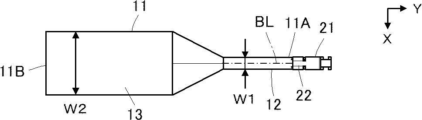
フレキシブル導体11は、一端部11Aから他端部11Bまで所定の方向に延びる帯形状の導電繊維からなり、一端部11Aに第1接続部12が配置され、他端部11Bに第2接続部13が配置されている。第1接続部12は、フレキシブル導体11の一端部11Aが、所定の方向に沿った折り曲げ線BLで二つ折りにして重ね合わされることにより形成されている。フレキシブル導体11の他端部11Bに配置された第2接続部13は、二つ折りにされることなく平面状に延びている。
コンタクト21は、一端に形成されたコンタクト側接続部22を有しており、フレキシブル導体11の第1接続部12がコンタクト側接続部22で第1接続部12の厚さ方向の両側から押しつけられることにより、コンタクト21がフレキシブル導体11に電気的に接続されている。
The
The
ここで、便宜上、フレキシブル導体11の他端部11Bが延びる平面をXY面、フレキシブル導体11の他端部11Bから一端部11Aに向かってフレキシブル導体11が延びる所定の方向を+Y方向、XY面に垂直に延びる方向をZ方向と呼ぶことにする。
Here, for convenience, the plane in which the
フレキシブル導体11の一端部11Aに形成された第1接続部12は、フレキシブル導体11を折り曲げ線BLで二つ折りにすることにより、YZ面に沿って延びる平板形状を有している。このため、図2に示されるように、二つ折りにされることなくXY面に沿って平面状に延びているフレキシブル導体11の他端部11Bに配置された第2接続部13が、X方向の幅W2を有するのに対して、フレキシブル導体11の一端部11Aに形成された第1接続部12は、第2接続部13の幅W2よりも狭いX方向の幅W1を有している。
The first connecting
コンタクト21のコンタクト側接続部22は、フレキシブル導体11の第1接続部12の+X方向側および-X方向側に配置された一対の挟み込み片22Aを有しており、図4に示されるように、フレキシブル導体11の第1接続部12は、一対の挟み込み片22Aにより、第1接続部12の厚さ方向であるX方向の両側から挟まれて押しつけられ、X方向に圧縮された状態で一対の挟み込み片22Aに接触している。
The contact-
次に、実施の形態1に係る接続構造を作製する方法について説明する。
まず、図5および図6に示されるように、Y方向に沿って延びる帯形状の導電繊維からなるフレキシブル導体11の一端部11Aにおいて、フレキシブル導体11のX方向の幅の中心線上にY方向に延びる折り曲げ線BLを規定する。なお、フレキシブル導体11の一端部11Aの-Z方向を向いた裏面には、接着剤14が塗布されているものとする。
Next, a method for manufacturing the connection structure according to
First, as shown in FIGS. 5 and 6, at one
次に、フレキシブル導体11の一端部11Aを、フレキシブル導体11の+Z方向を向いた表面が凸となるように、折り曲げ線BLで二つ折りにして、フレキシブル導体11の裏面同士を重ね合わせる。なお、導電繊維からなるフレキシブル導体11は、繊維の方向が折り曲げ線BLと同一のY方向に沿っており、折り曲げ線BLにより折り曲げやすくなっているものとする。フレキシブル導体11の一端部11Aの裏面には、接着剤14が塗布されているので、フレキシブル導体11の裏面同士が接着され、図7および図8に示されるように、フレキシブル導体11の一端部11Aに、YZ面に沿って延びる平板形状の第1接続部12が形成される。
Next, one
図9に示されるように、コンタクト21は、概ねL字状に屈曲された金属板から形成され、Y方向に延びる第1伸長部21Aと、第1伸長部21Aの+Y方向端部から+Z方向に延びる第2伸長部21Bとを有している。第1伸長部21Aの-Y方向端部にコンタクト側接続部22が配置され、第2伸長部21Bの+Z方向側に接触部23が配置され、コンタクト側接続部22と接触部23との間に保持部24が配置されている。
コンタクト側接続部22の一対の挟み込み片22Aは、+X方向および-X方向に向かって互いに反対方向に延びている。
また、接触部23の先端部は、第1伸長部21Aの+Z方向端部においてU字状に湾曲されている。
As shown in FIG. 9, the
The pair of sandwiching
Also, the tip of the
互いに反対方向に延びた一対の挟み込み片22Aを有するコンタクト側接続部22がフレキシブル導体11の第1接続部12の+Z方向側の縁部で且つ+Y方向端部に接触するように、コンタクト21をフレキシブル導体11に対して位置合わせした状態で、図10に示されるように、一対の挟み込み片22Aをそれぞれ-Z方向に屈曲させて一対の挟み込み片22Aにより第1接続部12を厚さ方向であるX方向の両側から挟み込んで押しつける。これにより、図1~図4に示されるように、コンタクト21がフレキシブル導体11に電気的に接続された接続構造が得られる。
The
フレキシブル導体11の一端部11Aを折り曲げ線BLで二つ折りにして重ね合わせることによりYZ面に沿って延びる平板形状の第1接続部12を形成し、コンタクト21のコンタクト側接続部22で第1接続部12の厚さ方向であるX方向の両側から押しつけることで、フレキシブル導体11とコンタクト21とを接続するので、Z方向から見たときの第1接続部12の占有面積を縮小しつつ、フレキシブル導体11とコンタクト21との間の実効的な接触面積を確保することができる。
One
実施の形態1に係る接続構造を利用することにより構成されたコネクタを図11~図14に示す。コネクタは、Z方向に延びる嵌合軸C1に沿って図示しない相手側コネクタと嵌合するもので、X方向に沿って2列に配列された複数のコンタクト21と、複数のコンタクト21を保持するハウジング31とを有している。それぞれの列の複数のコンタクト21は、嵌合軸C1に対して直交するX方向に沿って配列ピッチPで配列されている。複数のコンタクト21には、嵌合軸C1に垂直なXY面内において、嵌合軸C1を中心としてほぼ放射状に延びるように配列された複数のフレキシブル導体11が接続されており、それぞれのコンタクト21は、図1~図4に示される接続構造により対応するフレキシブル導体11に接続されている。
FIGS. 11 to 14 show connectors constructed by using the connection structure according to the first embodiment. The connector mates with a mating connector (not shown) along a mating axis C1 extending in the Z direction, and holds a plurality of
なお、複数のコンタクト21の配列ピッチPは、嵌合軸C1に沿った方向から見たときに、複数のフレキシブル導体11のそれぞれの第1接続部12の幅W1よりも広く、且つ、複数のフレキシブル導体11のそれぞれの第2接続部13の幅W2よりも狭い値を有している。
The arrangement pitch P of the plurality of
また、コネクタは、ハウジング31の周辺部を+Z方向から覆う外装部材41と、放射状に配列された複数のフレキシブル導体11の全体を+Z方向から覆う円形の上部カバー51と、放射状に配列された複数のフレキシブル導体11の第1接続部12を-Z方向から覆う円形の下部カバー61とを有している。
ハウジング31および外装部材41は、絶縁性樹脂から形成され、上部カバー51および下部カバー61は、可撓性を有する絶縁性繊維または絶縁性樹脂フィルムから形成されている。
The connector includes an
下部カバー61は、上部カバー51の直径よりも小さい直径を有しており、図13に示されるように、複数のフレキシブル導体11の他端部11Bに配置された第2接続部13は、下部カバー61により覆われることなく露出している。上部カバー51と下部カバー61により、複数のフレキシブル導体11の第1接続部12を覆いつつ第2接続部13を露出させるカバー部材が構成されている。
The
図15~図17は、図11~図13に示されるコネクタから、ハウジング31、外装部材41、上部カバー51および下部カバー61の図示を省略することにより、コネクタ内に配列された複数の接続構造のみを示す図である。それぞれの接続構造は、互いに対応するコンタクト21のコンタクト側接続部22とフレキシブル導体11の第1接続部12とが接続されたものである。複数のコンタクト21が、X方向に沿って2列に配列されているのに対して、複数のコンタクト21に接続される複数のフレキシブル導体11の第1接続部12をそれぞれXY面内で屈曲させることにより、複数のフレキシブル導体11の第2接続部13は、嵌合軸C1に垂直なXY面内において、嵌合軸C1を中心としてほぼ円形を描くように周方向に整列している。
15 to 17 show a plurality of connection structures arranged in the connector by omitting the illustration of the
図18および図19に示されるように、ハウジング31は、下部インシュレータ32と、下部インシュレータ32の上に配置される上部インシュレータ33とから形成されている。
それぞれ対応するコンタクト21のコンタクト側接続部22が接続された複数のフレキシブル導体11の第1接続部12が、下部インシュレータ32により保持され、複数のコンタクト21の第2伸長部21Bが、上部インシュレータ33により保持されている。
As shown in FIGS. 18 and 19 ,
The first connecting
下部インシュレータ32は、図20および図21に示されるように、XY面上に延びる円板形状を有しており、下部インシュレータ32の+Y方向側部分および-Y方向側部分に、それぞれY方向に沿って延び且つX方向に等間隔に配列された複数のスロット32Aが形成されている。複数のスロット32Aは、複数のフレキシブル導体11の第1接続部12を挿入して保持するためのものである。
As shown in FIGS. 20 and 21, the
上部インシュレータ33は、図22および図23に示されるように、XY面上に延びる平板形状の基部33Aと、基部33Aから+Z方向に突出し且つX方向に沿って延びるほぼ直方体形状の突状部33Bとを有している。突状部33Bの+Y方向側部分および-Y方向側部分に、それぞれZ方向に延びる複数のコンタクト保持溝33Cが形成され、基部33Aには、突状部33Bの複数のコンタクト保持溝33Cに連通する複数の貫通孔33Dが形成されている。複数のコンタクト保持溝33Cおよび複数の貫通孔33Dは、複数のコンタクト21の第2伸長部21Bを保持するためのものである。
As shown in FIGS. 22 and 23, the
上部インシュレータ33の複数のコンタクト保持溝33Cおよび複数の貫通孔33Dは、下部インシュレータ32の複数のスロット32Aに対応するように形成されている。すなわち、下部インシュレータ32の上に上部インシュレータ33が配置されると、下部インシュレータ32の複数のスロット32Aが、それぞれ、上部インシュレータ33の対応する貫通孔33Dおよびコンタクト保持溝33Cに連通するように構成されている。
A plurality of
ハウジング31の周辺部を+Z方向から覆う外装部材41は、図24および図25に示されるように、XY面上に延びる円板形状を有しており、外装部材41の中心部にX方向に延びる矩形の開口部41Aが形成されると共に、外装部材41の外周縁から-Z方向に突出する環状の突起41Bが形成されている。開口部41Aは、ハウジング31の上部インシュレータ33の突状部33Bが挿入される大きさを有している。
As shown in FIGS. 24 and 25, the
図15~図17に示されるように、それぞれ対応するフレキシブル導体11に接続された複数のコンタクト21がX方向に沿って2列に配列された状態で、図示しない成形型を用いて複数のコンタクト21と共に上部インシュレータ33を一体成形することができる。それぞれのコンタクト21の保持部24が上部インシュレータ33の対応する貫通孔33D内に埋設され、接触部23が上部インシュレータ33の対応するコンタクト保持溝33Cに保持されつつ上部インシュレータ33の突状部33Bから外方に向かって露出される。
As shown in FIGS. 15 to 17, a plurality of
予め絶縁性樹脂を成形することにより作製された下部インシュレータ32を-Z方向から上部インシュレータ33の-Z方向側の面に接触するまで+Z方向に移動させ、複数のコンタクト21のコンタクト側接続部22に接続された複数のフレキシブル導体11の第1接続部12を下部インシュレータ32の複数のスロット32Aに挿入して保持することで、複数のコンタクト21を保持するハウジング31が形成される。
The
その後、図18および図19に示されるように、嵌合軸C1を中心としてほぼ放射状に延びている複数のフレキシブル導体11の全体を+Z方向から円形の上部カバー51で覆い、複数のフレキシブル導体11の第1接続部12を-Z方向から円形の下部カバー61で覆い、外装部材41を+Z方向から上部カバー51の上に被せて、上部インシュレータ33の突状部33Bを外装部材41の開口部41Aから+Z方向に突出させる。
Thereafter, as shown in FIGS. 18 and 19, the plurality of
なお、上部カバー51の中心には、上部インシュレータ33の基部33Aが挿入される開口部51Aが形成されており、上部カバー51は、下部インシュレータ32と、複数のコンタクト21の第2伸長部21Bと、複数のフレキシブル導体11の上に配置され、外装部材41は、上部インシュレータ33の基部33Aと上部カバー51の上に配置される。また、下部カバー61は、下部インシュレータ32と、複数のフレキシブル導体11の第1接続部12の-Z方向側に配置される。
これにより、図11~図14に示されるコネクタが製造される。
An
This produces the connector shown in FIGS. 11-14.
このようにして製造されたコネクタに用いられている接続構造は、図1~図3に示されるように、フレキシブル導体11の一端部11Aを折り曲げ線BLで二つ折りにして重ね合わせることで形成された平板形状の第1接続部12を、コンタクト21のコンタクト側接続部22で第1接続部12の厚さ方向の両側から押しつけることにより、フレキシブル導体11とコンタクト21とを接続するものである。このため、それぞれ対応するフレキシブル導体11に接続された複数のコンタクト21を嵌合軸C1に対して直交する方向に配列したときに、複数のフレキシブル導体11を嵌合軸C1に垂直な面内において嵌合軸C1を中心としてほぼ放射状に延びるように配列することで、複数のコンタクト21の配列ピッチPを、それぞれのフレキシブル導体11の第2接続部13の幅W2よりも狭くすることができ、複数のコンタクト21を配列する際の狭ピッチ化を実現することが可能となる。
1 to 3, the connection structure used in the connector manufactured in this manner is formed by folding one
図11~図14に示されるコネクタは、例えば、衣服に装着され、複数のフレキシブル導体11の第2接続部13を衣服に形成されている複数の導電部材に電気的に接続することで、いわゆるウエアラブルデバイス用のコネクタとして利用することができる。
The connector shown in FIGS. 11 to 14 is attached to, for example, clothing, and electrically connects the second connecting
なお、折り曲げ線BLで二つ折りにされたフレキシブル導体11の裏面同士が、フレキシブル導体11の一端部11Aの裏面に塗布されている接着剤14により接着されているが、接着剤14の代わりに、例えば両面接着テープを用いて接着することもできる。
二つ折りにされたフレキシブル導体11の裏面同士は、必ずしも接着される必要はないが、それぞれ対応するフレキシブル導体11に接続された複数のコンタクト21を配列ピッチPで配列したときに、隣接するフレキシブル導体11の第1接続部12が互いに短絡することを防ぐために、二つ折りにされたフレキシブル導体11の裏面同士を接着することが望ましい。
The back surfaces of the
The back surfaces of the
また、ハウジング31の上部インシュレータ33は、複数のコンタクト21と共に一体成形されているが、これに限るものではなく、予め絶縁性樹脂を成形することにより作製された上部インシュレータ33に、複数のコンタクト21を圧入することで、複数のコンタクト21が上部インシュレータ33に保持されるように構成することもできる。
上部インシュレータ33に複数のコンタクト21を組み込んだ後に、それぞれのコンタクト21のコンタクト側接続部22に対応するフレキシブル導体11の第1接続部12を接続してもよい。
In addition, the
After assembling the plurality of
実施の形態2
図26~図28に実施の形態2に係る接続構造を示す。この接続構造は、実施の形態1で用いられたフレキシブル導体11の第1接続部12に導電性を有するコンタクト71を接続したものである。
コンタクト71は、一端に形成されたコンタクト側接続部72を有し、コンタクト側接続部72に形成されている、切り込み72Aにフレキシブル導体11の第1接続部12が挿入されることにより、コンタクト71がフレキシブル導体11に電気的に接続される。
26 to 28 show connection structures according to the second embodiment. In this connection structure, a
The
図29に示されるように、コンタクト71は、実施の形態1で用いられたコンタクト21において、コンタクト側接続部22の代わりにコンタクト側接続部72が第1伸長部21Aの-Y方向端部に配置されたものであり、その他の構成は、コンタクト21と同様である。
コンタクト側接続部72は、第1伸長部21Aの-Y方向端部から-Z方向に屈曲されてZ方向に延びており、コンタクト側接続部72の-Z方向端部からZ方向に沿って切り込み72Aが形成されている。
As shown in FIG. 29, a
The contact-
切り込み72Aにフレキシブル導体11の第1接続部12を挿入することで、切り込み72Aの内面により、第1接続部12は厚さ方向であるX方向の両側から押しつけられ、フレキシブル導体11とコンタクト71とが電気的に接続される。
このような実施の形態2の接続構造を利用しても、実施の形態1と同様にして、複数のコンタクト71を配列する際の狭ピッチ化を実現することが可能となる。
By inserting the
Even if such a connection structure of the second embodiment is used, it is possible to achieve a narrower pitch when arranging the
実施の形態3
図30に実施の形態3に係る接続構造を示す。実施の形態3の接続構造は、実施の形態1で用いられたフレキシブル導体11の第1接続部12に導電性を有するコンタクト81を接続したものである。
コンタクト81は、実施の形態1で用いられたコンタクト21において、第2伸長部21Bの代わりに、第2伸長部21BよりもZ方向長さが短い第2伸長部81Bが第1伸長部21Aの+Y方向端部に連結されたものであり、その他の構成は、コンタクト21と同様である。
FIG. 30 shows a connection structure according to the third embodiment. In the connection structure of the third embodiment, a
The
第2伸長部81Bの+Z方向端部は、+Y方向に屈曲しており、+Z方向を向いた平面状の接触部83が形成されている。この接触部83は、コンタクト81の+Z方向側においてXY面に沿って延びる図示しない回路基板の導電部に半田付け等により接続されるものである。
実施の形態3の接続構造を用いることにより、フレキシブル導体11を回路基板に接続することができると共に、実施の形態1と同様に、複数のコンタクト81を配列する際の狭ピッチ化を実現することが可能となる。
The +Z direction end of the second
By using the connection structure of the third embodiment, it is possible to connect the
なお、コンタクト81は、実施の形態1で用いられたコンタクト21と同様に、コンタクト側接続部22の一対の挟み込み片22Aにより、フレキシブル導体11の第1接続部12を厚さ方向であるX方向の両側から挟み込んで、フレキシブル導体11との電気的接続を図っている。ただし、実施の形態2におけるコンタクト71と同様に、コンタクト81が、コンタクト側接続部22の代わりに切り込み72Aを有するコンタクト側接続部72を備えていてもよい。このようにしても、フレキシブル導体11を回路基板に接続することができ、また、複数のコンタクト81を配列する際の狭ピッチ化を実現することが可能となる。
また、コンタクト81の接触部83の形状は、図30に示されるものに限られず、種々に変形可能である。
In the
Further, the shape of the
1 ベース部材、2 枠部材、3 布、4,6 開口部、5 導体部、7 コンタクト、7A 接点部、7B 外部接続部、8 突起、11 フレキシブル導体、11A 一端部(先端部)、11B 他端部、12 第1接続部、13 第2接続部、14 接着剤、21,71,81 コンタクト、21A 第1伸長部、21B,81B 第2伸長部、22,72 コンタクト側接続部、22A 挟み込み片、23,83 接触部、24 保持部、31 ハウジング、32 下部インシュレータ、32A スロット、33 上部インシュレータ、33A 基部、33B 突状部、33C コンタクト保持溝、33D 貫通孔、41 外装部材、41A 開口部、41B 突起、51 上部カバー、61 下部カバー、72A 切り込み、BL 折り曲げ線、W1,W2 幅、C1 嵌合軸、P 配列ピッチ。
1 base member, 2 frame member, 3 cloth, 4, 6 opening, 5 conductor, 7 contact, 7A contact, 7B external connection, 8 protrusion, 11 flexible conductor, 11A one end (tip), 11B, etc. end 12 first connecting
Claims (6)
前記複数のコンタクトに接続され且つそれぞれ所定の方向に延びる複数のフレキシブル導体と、
前記複数のコンタクトを保持するハウジングと
を備え、
前記複数のコンタクトは、それぞれ、
一端に配置され且つ対応する前記フレキシブル導体に接続されるコンタクト側接続部と、
他端に配置され且つ嵌合軸に沿って相手側コネクタと嵌合する際に前記相手側コネクタの対応するコンタクトに接触する接触部と、
前記コンタクト側接続部と前記接触部との間に配置され且つ前記ハウジングに埋設されて保持される保持部と
を有し、
前記複数のフレキシブル導体は、それぞれ、
前記所定の方向における一端部を前記所定の方向に沿った折り曲げ線で二つ折りにして重ね合わせることにより形成された第1接続部と、
前記所定の方向における他端部に配置された第2接続部と
を有し、
前記複数のコンタクトは、それぞれ、前記コンタクト側接続部が、対応する前記フレキシブル導体の前記第1接続部を前記第1接続部の厚さ方向の両側から押しつけることにより、前記フレキシブル導体に電気的に接続され、
前記複数のコンタクトは、前記嵌合軸に対して直交する方向に配列され、
前記複数のフレキシブル導体は、前記嵌合軸に垂直な面内において、前記嵌合軸を中心としてほぼ放射状に延びているコネクタ。 a plurality of electrically conductive contacts;
a plurality of flexible conductors connected to the plurality of contacts and extending in predetermined directions;
a housing that holds the plurality of contacts,
Each of the plurality of contacts includes:
a contact-side connecting portion arranged at one end and connected to the corresponding flexible conductor;
a contact portion arranged at the other end and brought into contact with the corresponding contact of the mating connector when mating with the mating connector along the mating axis;
a holding portion disposed between the contact-side connection portion and the contact portion and embedded and held in the housing;
Each of the plurality of flexible conductors is:
a first connecting portion formed by folding one end portion in the predetermined direction in two along a folding line along the predetermined direction and overlapping the first connecting portion;
and a second connection portion arranged at the other end in the predetermined direction,
Each of the plurality of contacts is electrically connected to the flexible conductor by the contact-side connecting portion pressing the corresponding first connecting portion of the flexible conductor from both sides in the thickness direction of the first connecting portion. connected and
The plurality of contacts are arranged in a direction perpendicular to the mating axis,
A connector in which the plurality of flexible conductors extend substantially radially about the fitting axis in a plane perpendicular to the fitting axis .
Priority Applications (4)
| Application Number | Priority Date | Filing Date | Title |
|---|---|---|---|
| JP2019093645A JP7249201B2 (en) | 2019-05-17 | 2019-05-17 | Connection method, connection structure, contact and connector |
| CN202010118052.4A CN111952815B (en) | 2019-05-17 | 2020-02-25 | Connection method, connection structure, contact, and connector |
| US16/803,334 US11398689B2 (en) | 2019-05-17 | 2020-02-27 | Connecting method, connecting structure, contact and connector |
| EP20164342.6A EP3739690B1 (en) | 2019-05-17 | 2020-03-19 | Connecting method, connecting structure, contact and connector |
Applications Claiming Priority (1)
| Application Number | Priority Date | Filing Date | Title |
|---|---|---|---|
| JP2019093645A JP7249201B2 (en) | 2019-05-17 | 2019-05-17 | Connection method, connection structure, contact and connector |
Publications (2)
| Publication Number | Publication Date |
|---|---|
| JP2020187981A JP2020187981A (en) | 2020-11-19 |
| JP7249201B2 true JP7249201B2 (en) | 2023-03-30 |
Family
ID=69903062
Family Applications (1)
| Application Number | Title | Priority Date | Filing Date |
|---|---|---|---|
| JP2019093645A Active JP7249201B2 (en) | 2019-05-17 | 2019-05-17 | Connection method, connection structure, contact and connector |
Country Status (4)
| Country | Link |
|---|---|
| US (1) | US11398689B2 (en) |
| EP (1) | EP3739690B1 (en) |
| JP (1) | JP7249201B2 (en) |
| CN (1) | CN111952815B (en) |
Families Citing this family (2)
| Publication number | Priority date | Publication date | Assignee | Title |
|---|---|---|---|---|
| JP1645875S (en) * | 2019-05-27 | 2019-11-18 | ||
| JP7438085B2 (en) * | 2020-11-18 | 2024-02-26 | 日本航空電子工業株式会社 | connector |
Citations (2)
| Publication number | Priority date | Publication date | Assignee | Title |
|---|---|---|---|---|
| US20170279105A1 (en) | 2016-03-24 | 2017-09-28 | Tyco Electronics Corporation | Terminal assembly with a multi-wire planar cable |
| JP2018101503A (en) | 2016-12-19 | 2018-06-28 | 日本航空電子工業株式会社 | Slide type connector |
Family Cites Families (13)
| Publication number | Priority date | Publication date | Assignee | Title |
|---|---|---|---|---|
| DE7821233U1 (en) * | 1978-07-14 | 1978-10-26 | Raychem Gmbh, 8011 Putzbrunn | Connectors for ribbon cables |
| JPS6016574U (en) * | 1983-07-13 | 1985-02-04 | 株式会社東芝 | flexible printed wiring board |
| DE9102716U1 (en) * | 1990-03-16 | 1991-05-23 | Minnesota Mining & Mfg. Co., Saint Paul, Minn. | Device for connecting a plurality of at least partially insulated conductors to electrical contacts |
| JPH09180797A (en) * | 1995-12-22 | 1997-07-11 | Furukawa Electric Co Ltd:The | Flat cable connection terminal |
| JP2001307559A (en) * | 2000-04-19 | 2001-11-02 | Sumitomo Wiring Syst Ltd | Wiring material and structure of its connection |
| US6394833B1 (en) * | 2001-04-25 | 2002-05-28 | Miraco, Inc. | Flat flexible cable connector |
| US6710251B2 (en) * | 2001-05-22 | 2004-03-23 | Electric Motion Company, Inc. | Fiber optic cable shield bond system |
| JP2003031288A (en) * | 2001-07-18 | 2003-01-31 | Yazaki Corp | Flat circuit body and method for manufacturing the same |
| US6811441B2 (en) * | 2002-05-10 | 2004-11-02 | Fci Americas Technology, Inc. | Electrical cable strain relief and electrical closure |
| JP4036370B2 (en) * | 2003-06-02 | 2008-01-23 | 日本航空電子工業株式会社 | Electrical connector and manufacturing method thereof |
| US8932084B2 (en) * | 2013-01-25 | 2015-01-13 | Tyco Electronics Corporation | Connector system |
| JP6734676B2 (en) * | 2016-03-28 | 2020-08-05 | 日本航空電子工業株式会社 | Sliding connector |
| JP6792493B2 (en) | 2017-03-17 | 2020-11-25 | 日本航空電子工業株式会社 | connector |
-
2019
- 2019-05-17 JP JP2019093645A patent/JP7249201B2/en active Active
-
2020
- 2020-02-25 CN CN202010118052.4A patent/CN111952815B/en active Active
- 2020-02-27 US US16/803,334 patent/US11398689B2/en active Active
- 2020-03-19 EP EP20164342.6A patent/EP3739690B1/en active Active
Patent Citations (2)
| Publication number | Priority date | Publication date | Assignee | Title |
|---|---|---|---|---|
| US20170279105A1 (en) | 2016-03-24 | 2017-09-28 | Tyco Electronics Corporation | Terminal assembly with a multi-wire planar cable |
| JP2018101503A (en) | 2016-12-19 | 2018-06-28 | 日本航空電子工業株式会社 | Slide type connector |
Also Published As
| Publication number | Publication date |
|---|---|
| CN111952815B (en) | 2023-03-31 |
| CN111952815A (en) | 2020-11-17 |
| US11398689B2 (en) | 2022-07-26 |
| EP3739690B1 (en) | 2022-05-04 |
| EP3739690A1 (en) | 2020-11-18 |
| JP2020187981A (en) | 2020-11-19 |
| US20200366010A1 (en) | 2020-11-19 |
Similar Documents
| Publication | Publication Date | Title |
|---|---|---|
| US10617155B2 (en) | Connector attached on opposite sides of garment and sandwiched between connector first member and connector second member | |
| JP6734676B2 (en) | Sliding connector | |
| JP7348060B2 (en) | Connector and connection method | |
| US20210104824A1 (en) | Connector and connecting method | |
| JP7313991B2 (en) | connector | |
| JP7249201B2 (en) | Connection method, connection structure, contact and connector | |
| EP3790115B1 (en) | Connector and connecting method | |
| US11211726B2 (en) | Connector and connecting method | |
| JP7265458B2 (en) | Connector and connection method | |
| EP3799218B1 (en) | Connector | |
| JP2020129435A (en) | Female contact | |
| CN112636040B (en) | Connector having holding member for holding conductive member | |
| KR20140062550A (en) | Interposer and method for manufacturing the same | |
| JP7144332B2 (en) | Connector, wiring board assembly and connection structure | |
| JP3551289B2 (en) | Electronic component mounting socket and electronic component accommodated in the electronic component mounting socket | |
| JP6858949B2 (en) | Contacts, connector members and connectors | |
| JP7348024B2 (en) | Connector and connection method | |
| TWM620947U (en) | Wire connector assembly | |
| JP3935097B2 (en) | connector | |
| JP2024003335A (en) | Sheet-shaped conductive member and connector | |
| JP2024078683A (en) | Connector assembly and connecting method | |
| JP2000100523A (en) | Shield connector |
Legal Events
| Date | Code | Title | Description |
|---|---|---|---|
| A621 | Written request for application examination |
Free format text: JAPANESE INTERMEDIATE CODE: A621 Effective date: 20220112 |
|
| A977 | Report on retrieval |
Free format text: JAPANESE INTERMEDIATE CODE: A971007 Effective date: 20221025 |
|
| A131 | Notification of reasons for refusal |
Free format text: JAPANESE INTERMEDIATE CODE: A131 Effective date: 20221101 |
|
| A521 | Request for written amendment filed |
Free format text: JAPANESE INTERMEDIATE CODE: A523 Effective date: 20221207 |
|
| TRDD | Decision of grant or rejection written | ||
| A01 | Written decision to grant a patent or to grant a registration (utility model) |
Free format text: JAPANESE INTERMEDIATE CODE: A01 Effective date: 20230314 |
|
| A61 | First payment of annual fees (during grant procedure) |
Free format text: JAPANESE INTERMEDIATE CODE: A61 Effective date: 20230317 |
|
| R150 | Certificate of patent or registration of utility model |
Ref document number: 7249201 Country of ref document: JP Free format text: JAPANESE INTERMEDIATE CODE: R150 |