JP7246591B1 - optical semiconductor device - Google Patents
optical semiconductor device Download PDFInfo
- Publication number
- JP7246591B1 JP7246591B1 JP2023503168A JP2023503168A JP7246591B1 JP 7246591 B1 JP7246591 B1 JP 7246591B1 JP 2023503168 A JP2023503168 A JP 2023503168A JP 2023503168 A JP2023503168 A JP 2023503168A JP 7246591 B1 JP7246591 B1 JP 7246591B1
- Authority
- JP
- Japan
- Prior art keywords
- layer
- light absorption
- absorption layer
- scattered light
- semiconductor device
- Prior art date
- Legal status (The legal status is an assumption and is not a legal conclusion. Google has not performed a legal analysis and makes no representation as to the accuracy of the status listed.)
- Active
Links
- 239000004065 semiconductor Substances 0.000 title claims abstract description 183
- 230000003287 optical effect Effects 0.000 title claims abstract description 180
- 230000031700 light absorption Effects 0.000 claims abstract description 170
- 239000013078 crystal Substances 0.000 claims abstract description 49
- 239000000758 substrate Substances 0.000 claims abstract description 28
- 238000005253 cladding Methods 0.000 claims abstract description 10
- 230000004888 barrier function Effects 0.000 claims description 29
- 230000008033 biological extinction Effects 0.000 description 24
- 230000000694 effects Effects 0.000 description 17
- 229910000530 Gallium indium arsenide Inorganic materials 0.000 description 13
- 238000010521 absorption reaction Methods 0.000 description 13
- 238000000034 method Methods 0.000 description 12
- 230000007423 decrease Effects 0.000 description 8
- 230000006870 function Effects 0.000 description 8
- 238000004519 manufacturing process Methods 0.000 description 7
- 239000000463 material Substances 0.000 description 7
- 238000000926 separation method Methods 0.000 description 7
- 238000005530 etching Methods 0.000 description 6
- 230000002829 reductive effect Effects 0.000 description 6
- 238000004891 communication Methods 0.000 description 5
- 238000010586 diagram Methods 0.000 description 4
- 230000008569 process Effects 0.000 description 4
- 230000008859 change Effects 0.000 description 3
- 238000005566 electron beam evaporation Methods 0.000 description 3
- 238000005516 engineering process Methods 0.000 description 3
- XEEYBQQBJWHFJM-UHFFFAOYSA-N iron Substances [Fe] XEEYBQQBJWHFJM-UHFFFAOYSA-N 0.000 description 3
- 230000007246 mechanism Effects 0.000 description 3
- 239000013307 optical fiber Substances 0.000 description 3
- 238000000206 photolithography Methods 0.000 description 3
- 230000001681 protective effect Effects 0.000 description 3
- 229910004298 SiO 2 Inorganic materials 0.000 description 2
- 238000000862 absorption spectrum Methods 0.000 description 2
- 230000002411 adverse Effects 0.000 description 2
- 230000008901 benefit Effects 0.000 description 2
- 230000005540 biological transmission Effects 0.000 description 2
- 239000000969 carrier Substances 0.000 description 2
- 230000008878 coupling Effects 0.000 description 2
- 238000010168 coupling process Methods 0.000 description 2
- 238000005859 coupling reaction Methods 0.000 description 2
- 230000006866 deterioration Effects 0.000 description 2
- 239000012535 impurity Substances 0.000 description 2
- 238000002955 isolation Methods 0.000 description 2
- 239000002184 metal Substances 0.000 description 2
- 229910052751 metal Inorganic materials 0.000 description 2
- 238000012545 processing Methods 0.000 description 2
- 230000009467 reduction Effects 0.000 description 2
- 230000002441 reversible effect Effects 0.000 description 2
- 230000002195 synergetic effect Effects 0.000 description 2
- 240000007594 Oryza sativa Species 0.000 description 1
- 235000007164 Oryza sativa Nutrition 0.000 description 1
- 229910052787 antimony Inorganic materials 0.000 description 1
- WATWJIUSRGPENY-UHFFFAOYSA-N antimony atom Chemical compound [Sb] WATWJIUSRGPENY-UHFFFAOYSA-N 0.000 description 1
- 229910052797 bismuth Inorganic materials 0.000 description 1
- JCXGWMGPZLAOME-UHFFFAOYSA-N bismuth atom Chemical compound [Bi] JCXGWMGPZLAOME-UHFFFAOYSA-N 0.000 description 1
- 238000005229 chemical vapour deposition Methods 0.000 description 1
- 238000002109 crystal growth method Methods 0.000 description 1
- 230000003247 decreasing effect Effects 0.000 description 1
- 238000001312 dry etching Methods 0.000 description 1
- 230000005684 electric field Effects 0.000 description 1
- 230000005284 excitation Effects 0.000 description 1
- 238000000605 extraction Methods 0.000 description 1
- 230000006872 improvement Effects 0.000 description 1
- 229910052742 iron Inorganic materials 0.000 description 1
- 210000001503 joint Anatomy 0.000 description 1
- 230000004048 modification Effects 0.000 description 1
- 238000012986 modification Methods 0.000 description 1
- 230000010355 oscillation Effects 0.000 description 1
- 230000001902 propagating effect Effects 0.000 description 1
- 230000004044 response Effects 0.000 description 1
- 235000009566 rice Nutrition 0.000 description 1
- 238000012216 screening Methods 0.000 description 1
- 238000001228 spectrum Methods 0.000 description 1
- 238000000992 sputter etching Methods 0.000 description 1
- 238000001039 wet etching Methods 0.000 description 1
Images


Classifications
-
- H—ELECTRICITY
- H01—ELECTRIC ELEMENTS
- H01S—DEVICES USING THE PROCESS OF LIGHT AMPLIFICATION BY STIMULATED EMISSION OF RADIATION [LASER] TO AMPLIFY OR GENERATE LIGHT; DEVICES USING STIMULATED EMISSION OF ELECTROMAGNETIC RADIATION IN WAVE RANGES OTHER THAN OPTICAL
- H01S5/00—Semiconductor lasers
- H01S5/02—Structural details or components not essential to laser action
- H01S5/026—Monolithically integrated components, e.g. waveguides, monitoring photo-detectors, drivers
Abstract
本開示の光半導体装置(100)は、共通の半導体基板(1)上に形成された半導体レーザ部(70)及び光変調器部(72)を有する光半導体装置(100)であって、半導体レーザ部(70)は、それぞれIII-V族半導体混晶からなる第1導電型の下部クラッド層(2)、レーザ光を発する活性層(3)、一次の回折格子(15)が設けられた第2導電型の上部クラッド層(4)の各層を備え、光変調器部(72)は、少なくとも一部がBiを含有するIII-V族半導体混晶からなり活性層(3)から入射するレーザ光を吸収する光吸収層(21)と、光吸収層(21)の下面及び上面のいずれか一方の面に対向する散乱光吸収層(20、22)または光吸収層(21)の下面及び上面にそれぞれ対向する一対の散乱光吸収層(20、22)と、を備える。An optical semiconductor device (100) of the present disclosure is an optical semiconductor device (100) having a semiconductor laser section (70) and an optical modulator section (72) formed on a common semiconductor substrate (1), comprising: The laser section (70) is provided with a first conductivity type lower clad layer (2) made of a group III-V semiconductor mixed crystal, an active layer (3) for emitting laser light, and a first-order diffraction grating (15). Equipped with each layer of the upper cladding layer (4) of the second conductivity type, the optical modulator section (72) is at least partially made of a III-V group semiconductor mixed crystal containing Bi, and light is incident from the active layer (3) A light absorption layer (21) that absorbs laser light, and scattered light absorption layers (20, 22) facing either the bottom surface or the top surface of the light absorption layer (21) or the bottom surface of the light absorption layer (21) and a pair of scattered light absorption layers (20, 22) facing each other on the upper surface.
Description
本開示は、光半導体装置に関する。 The present disclosure relates to an optical semiconductor device.
近年の各種情報端末の普及、情報のクラウド化などにともない、データ通信量が急激に増大しつつある。増大するデータ通信量の需要に対応するため、光ファイバ通信の基地局内の伝送速度の高速化及び大容量化が進んでいる。 With the recent spread of various information terminals and cloud computing of information, the amount of data communication is increasing rapidly. 2. Description of the Related Art In order to meet the increasing demand for data communication, the transmission speed and capacity in base stations for optical fiber communication are increasing.
光ファイバ通信の長距離光通信用光源として、光半導体装置の一種である、半導体レーザ部と光変調器部とをモノリシックに集積した光変調器付き半導体レーザ装置(Electro-absorption Modulator Laser Diode:EML-LD)が用いられている。光変調器部は外部変調器の一種であり、レーザ光強度を直接変調する直接変調方式に対して信号波形の劣化が少なく、高速かつ長距離の光ファイバ伝送が可能となる。 As a light source for long-distance optical communication of optical fiber communication, a semiconductor laser device with an optical modulator (Electro-absorption Modulator Laser Diode: EML), which is a type of optical semiconductor device, in which a semiconductor laser section and an optical modulator section are monolithically integrated. -LD) is used. The optical modulator section is a kind of external modulator, which has less signal waveform deterioration than the direct modulation method that directly modulates the laser light intensity, and enables high-speed and long-distance optical fiber transmission.
EML-LDでは、分布帰還型半導体レーザ(Distributed FeedBack Laser Diode:DFB-LD)で構成された半導体レーザ部と電界吸収型光変調器(Electro-absorption Modulator:EML)とで構成された光変調器部との結合部(バットジョイント)において、半導体レーザ部から入射したレーザ光の中で光変調器部の光吸収層に導波されなかった散乱光が、光変調器部の出射端面から外部に出射されて漏れ光となり、出力光のサイドピークとして現れ、EML-LDの光軸調整の妨げとなったり、消光比、つまり、光のオン・オフ状態における光強度比の低下の要因となっていた。EML-LDが高出力で動作するほど、EML-LDから外部に出射される漏れ光の強度も増大するため、ますます消光比が低下するという不具合が生じた。 In the EML-LD, an optical modulator composed of a semiconductor laser section composed of a distributed feedback semiconductor laser (DFB-LD) and an electro-absorption modulator (EML). At the joint (butt joint) with the part, the scattered light that is not guided to the light absorption layer of the optical modulator part in the laser light that is incident from the semiconductor laser part is emitted from the output end face of the optical modulator part to the outside. Leaked light is emitted and appears as a side peak of the output light, which hinders the optical axis adjustment of the EML-LD and causes a decrease in the extinction ratio, that is, the light intensity ratio in the ON/OFF state of the light. rice field. As the EML-LD operates at a higher output, the intensity of leakage light emitted from the EML-LD to the outside also increases, resulting in a problem that the extinction ratio further decreases.
EML-LDにおける消光比の低下を防止するために、例えば、特許文献1に記載の半導体発光装置では、光変調器部の出力端面に光吸収層の端面が開口した遮蔽膜が設けられている。
In order to prevent a decrease in the extinction ratio of the EML-LD, for example, in the semiconductor light emitting device described in
特許文献1に記載の半導体発光装置の光変調器部に設けられた遮蔽膜は、光吸収層以外の出射端面から出力される漏れ光を遮蔽するように機能する。遮蔽膜によって漏れ光を光変調器部の出射端面で確実に遮蔽することが可能となるので、光変調時の消光比が増大するという効果を奏する。
The shielding film provided in the optical modulator section of the semiconductor light-emitting device described in
しかしながら、光変調器部の出力端面に遮蔽膜を設けるには、出力端面の全面に金属膜を形成した後、開口部以外の部分をマスクしてイオンエッチング等により除去するという微細な加工が必要となるが、出力端面上の加工は非常に難度が高く、遮蔽膜として必要な加工精度を維持することは困難であった。したがって、漏れ光の小さい、すなわち消光比の高い光半導体装置を再現性良く製造するという点で問題があった。 However, in order to provide a shielding film on the output facet of the optical modulator section, a fine process is required to form a metal film on the entire surface of the output facet, mask the portion other than the opening, and remove it by ion etching or the like. However, the processing on the output end face is extremely difficult, and it has been difficult to maintain the processing accuracy required for the shielding film. Therefore, there is a problem in manufacturing an optical semiconductor device with a small leakage light, ie, a high extinction ratio, with good reproducibility.
本開示は上記のような問題点を解消するためになされたもので、高出力駆動時においても、消光比の高い光半導体装置を得ることを目的とする。 The present disclosure has been made to solve the above problems, and an object of the present disclosure is to obtain an optical semiconductor device having a high extinction ratio even during high-output driving.
本開示による光半導体装置は、
共通の半導体基板上に形成された半導体レーザ部及び光変調器部を有する光半導体装置であって、
前記半導体レーザ部は、
それぞれIII-V族半導体混晶からなる第1導電型の下部クラッド層、レーザ光を発する活性層、一次の回折格子が設けられた第2導電型の上部クラッド層の各層を備え、
前記光変調器部は、
少なくとも一部がBiを含有するIII-V族半導体混晶からなり、前記活性層から入射する前記レーザ光を吸収する光吸収層と、
前記光吸収層の下面及び上面のいずれか一方の面に対向する散乱光吸収層または前記光吸収層の下面及び上面にそれぞれ対向する一対の散乱光吸収層と、を備え、
前記光変調器部は、少なくとも前記光吸収層及び前記散乱光吸収層を含むメサストライプを有し、前記メサストライプの側面部に側面散乱光吸収層が設けられることを特徴とする。
An optical semiconductor device according to the present disclosure includes:
An optical semiconductor device having a semiconductor laser section and an optical modulator section formed on a common semiconductor substrate,
The semiconductor laser section is
Each layer of a first conductivity type lower clad layer made of a group III-V semiconductor mixed crystal, an active layer that emits laser light, and a second conductivity type upper clad layer provided with a first-order diffraction grating,
The optical modulator section
a light absorption layer at least partially made of a III-V group semiconductor mixed crystal containing Bi and absorbing the laser light incident from the active layer;
a scattered light absorption layer facing either one of the lower surface and the upper surface of the light absorption layer or a pair of scattered light absorption layers facing the lower surface and the upper surface of the light absorption layer, respectively ;
The optical modulator section has a mesa stripe including at least the light absorption layer and the scattered light absorption layer, and a side scattered light absorption layer is provided on a side surface of the mesa stripe.
本開示に係る光半導体装置によれば、光変調器部に設けられた散乱光吸収層が光吸収層に導波される導波光以外の散乱光を吸収するので、散乱光に起因する消光比の低下を防止することができ、さらに、光吸収層がBiを含有することにより、散乱光吸収層による散乱光の吸収により発生した熱によって発生する光吸収層内でのホールのパイルアップに起因する消光比の低下も同時に抑制できるので、消光比の高い光半導体装置が得られるという効果を奏する。 According to the optical semiconductor device according to the present disclosure, the scattered light absorption layer provided in the optical modulator section absorbs the scattered light other than the guided light guided by the light absorption layer, so the extinction ratio due to the scattered light Further, since the light absorption layer contains Bi, holes are piled up in the light absorption layer caused by heat generated by absorption of scattered light by the scattered light absorption layer. At the same time, it is possible to suppress the decrease in the extinction ratio, which causes an effect that an optical semiconductor device having a high extinction ratio can be obtained.
実施の形態1.
<実施の形態1に係る光半導体装置の構成>
図1は、実施の形態1に係る光半導体装置100における光の導波方向に沿った断面図である。実施の形態1に係る光半導体装置100の一例として、EML-LDを挙げている。
<Structure of Optical Semiconductor Device According to First Embodiment>
FIG. 1 is a cross-sectional view of the
実施の形態1に係る光半導体装置100は、半導体レーザ部70、分離部71、及び光変調器部72の各領域で構成されている。なお、以下の説明では、上下方向とは、半導体基板の表面に垂直な方向において、活性層あるいは光吸収層を基準として結晶成長層の表面側に向かう方向を上方向、半導体基板の裏面側に向かう方向を下方向とそれぞれ定義する。
The
半導体レーザ部70は、n型InP基板1(半導体基板1)上に順次形成されたn型InP下部クラッド層2(第1導電型の下部クラッド層2)、活性層3、p型InP上部第1クラッド層4(第2導電型の上部クラッド層4)、p型InP上部第2クラッド層5、p型InGaAs第1コンタクト層6aからなる各結晶成長層によって構成される。
The
p型InP上部第1クラッド層4中には、一次の回折格子15が形成されている。また、活性層3は、典型的には、InGaAsP多重量子井戸構造で構成される。
A first-order diffraction grating 15 is formed in the p-type InP upper
p型InGaAs第1コンタクト層6a上には、表面保護絶縁膜7aの開口部を介してp側第1電極8a及びp側第2電極9aがそれぞれ形成されている。n型InP基板1の裏面側には、n側第1電極10及びn側第2電極11がそれぞれ形成されている。
A p-side
光変調器部72は、n型InP基板1上に順次形成された下部散乱光吸収層20、n型InP下部クラッド層2、Bi(ビスマス)を含有するIII-V族半導体混晶であるi型InGaAsBiからなる光吸収層21、p型InP上部第1クラッド層4、上部散乱光吸収層22、p型InP上部第2クラッド層5、p型InGaAs第2コンタクト層6bからなる各結晶成長層によって構成される。なお、以下の説明では、下部散乱光吸収層20及び上部散乱光吸収層22のそれぞれを単に散乱光吸収層と呼ぶ場合もある。また、下部散乱光吸収層20及び上部散乱光吸収層22を総称して、一対の散乱光吸収層と呼ぶ場合もある。
The
p型InGaAs第2コンタクト層6b上には、表面保護絶縁膜7cの開口部を介してp側第3電極8b及びp側第4電極9bがそれぞれ形成されている。n型InP基板1の裏面側には、n側第1電極10及びn側第2電極11がそれぞれ形成されている。
A p-side
半導体レーザ部70、分離部71、及び光変調器部72は、共通のn型InP基板1上に形成されている。また、n側第1電極10及びn側第2電極11も、半導体レーザ部70、分離部71、及び光変調器部72において、一体となって形成されている。
The
分離部71は、p型InGaAs第2コンタクト層6bが設けられていないこと、表面が表面保護絶縁膜7bで覆われていること、p側第3電極8b及びp側第4電極9bが設けられていないことを除いて、光変調器部72と同一の構成である。
The
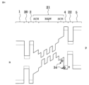
図2は、実施の形態1に係る光半導体装置100における光の導波方向に対して垂直方向の光変調器部72の断面図である。
FIG. 2 is a cross-sectional view of the
メサストライプ35は、両側面に設けられた一対のメサ溝35a、35bによって形成される。メサ溝35a、35bの底面部及び側面部は表面保護絶縁膜7cによって覆われている。メサストライプ35において、i型InGaAsBiからなる光吸収層21の両側面側には、高抵抗InP埋込層37a、37bがそれぞれ形成されている。高抵抗InPを構成する半導体材料の一例として、Fe(鉄)をドープした半絶縁性InPが挙げられる。
The
図3は、光変調器部72のi型InGaAsBiからなる光吸収層21を構成する多重量子井戸構造からなるMQW層31の断面図である。i型InGaAsBiからなる光吸収層21は、n型InP基板1側から、下部SCH層30a、ウエル層32及びバリア層33が交互に積層されたMQW層31、及び上部SCH層30bの各層で構成されている。なお、MQWとは、Multi Quantum Wellの略称であり多重量子井戸を意味する。また、SCHとは、Separate Confinement Heterostructureの略称であり、分離閉じ込め層を意味する。
FIG. 3 is a cross-sectional view of the
ウエル層32及びバリア層33、並びに下部SCH層30a及び上部SCH層30bは、いずれもBiを含有するIII-V族半導体混晶によって構成される。典型的には、i型InGaAsBiである。
The
<実施の形態1に係る光半導体装置の製造方法>
実施の形態1に係る光半導体装置100の製造方法の概要について、以下に説明する。<Method for Manufacturing Optical Semiconductor Device According to First Embodiment>
An overview of the method for manufacturing the
先ず、半導体レーザ部70の各結晶成長層を形成する工程を説明する。
n型InP基板1上において半導体レーザ部70の形成が予定されている領域に、n型InP下部クラッド層2、活性層3、及びp型InP上部第1クラッド層4の一部を、順次エピタキシャル結晶成長する。エピタキシャル結晶成長方法として、例えば有機金属気相成長法(Metal Organic Chemical Vapor Deposition:MOCVD)、分子線エピタキシャル成長法(Molecular Beam Epitaxy:MBE)などが挙げられる。First, the process of forming each crystal growth layer of the
The n-type InP lower clad
上述のエピタキシャル結晶成長後、フォトリソグラフィ技術及びエッチング技術を用いて、p型InP上部第1クラッド層4の表面に一次の回折格子15を形成する。回折格子15が形成されたp型InP上部第1クラッド層4上に、p型InP上部第1クラッド層4の残部、p型InP上部第2クラッド層5、及びp型InGaAs第1コンタクト層6aの各層を、MOCVD法などによって順次エピタキシャル結晶成長する。エピタキシャル結晶成長後、フォトリソグラフィ技術及びエッチング技術を用いて、半導体レーザ部70の表面に絶縁膜マスクをパターニング形成する。絶縁膜マスクを構成する材料としては、例えばSiO2が好適である。After the epitaxial crystal growth described above, a first-
次に、分離部71及び光変調器部72の各結晶成長層を形成する工程を説明する。n型InP基板1上において分離部71及び光変調器部72の形成が予定されている領域に、下部散乱光吸収層20、n型InP下部クラッド層2、i型InGaAsBiからなる光吸収層21、p型InP上部第1クラッド層4、上部散乱光吸収層22、p型InP上部第2クラッド層5、p型InGaAs第2コンタクト層6bの各結晶成長層を、MOCVD法などによって順次エピタキシャル結晶成長する。
Next, the process of forming each crystal growth layer of the
分離部71及び光変調器部72の各結晶成長層の形成後、半導体レーザ部70を覆っていた絶縁膜マスクを除去する。さらに、一対のメサ溝35a、35bの形成が予定されている部位以外を絶縁膜マスクで覆う。絶縁膜マスクを構成する材料としては、例えばSiO2が好適である。After forming the crystal growth layers of the separating
絶縁膜マスクをエッチングマスクとして、ドライエッチング、ウエットエッチングなどのエッチング技術によって、半導体レーザ部70において最表面の結晶成長層であるp型InGaAs第1コンタクト層6aからn型InP基板1に、分離部71において最表面の結晶成長層であるp型InP上部第2クラッド層5から下部散乱光吸収層20に、光変調器部72において最表面の結晶成長層であるp型InGaAs第2コンタクト層6bから下部散乱光吸収層20にそれぞれ達する一対のメサ溝35a、35bを形成する。
Using the insulating film mask as an etching mask, an etching technique such as dry etching or wet etching is performed to form a separating portion from the p-type InGaAs
一対のメサ溝35a、35bを形成後、絶縁膜マスクが残っている状態で、メサストライプ35の形成を予定している側の側面部に、高抵抗InP埋込層37a、37bをMOCVD法などによって埋込成長する。埋込成長後、不要な部位をエッチングなどによって除去することにより、メサストライプ35が完成する。
After forming the pair of
EML-LDの表面側の結晶成長層の全体を覆うように絶縁膜を形成して、フォトリソグラフィ技術及びエッチング技術を用いて、各電極の形成が予定される部位に開口部を設ける。形成された絶縁膜は表面保護絶縁膜7a、7b、7cとして機能する。半導体レーザ部70では、表面保護絶縁膜7aの開口部を介してp型InGaAs第1コンタクト層6aと接するp側第1電極8aと、p側第1電極8a上のp側第2電極9aとを、それぞれ電子ビーム蒸着などによって成膜し、リフトオフしてパターニングする。
An insulating film is formed so as to cover the entire crystal growth layer on the surface side of the EML-LD, and photolithography and etching techniques are used to form openings where electrodes are to be formed. The formed insulating films function as surface protective insulating
光変調器部72では、表面保護絶縁膜7cの開口部を介してp型InGaAs第2コンタクト層6bと接するp側第3電極8bと、p側第3電極8b上のp側第4電極9bとを、それぞれ電子ビーム蒸着などによって成膜し、リフトオフしてパターニングする。なお、半導体レーザ部70及び光変調器部72の電極形成は、同一の工程で行っても良い。
In the
n型InP基板1の裏面側に、n側第1電極10及びn側第2電極11を、それぞれ電子ビーム蒸着などによって成膜し、リフトオフしてパターニングする。へき開などにより、ウエハから個々のチップに分離することにより、EML-LDが完成する。
以上が、実施の形態1に係る光半導体装置100の一例であるEML-LDの製造方法の概要である。An n-side
The above is the outline of the manufacturing method of the EML-LD, which is an example of the
<実施の形態1に係る光半導体装置の動作>
まず、実施の形態1に係る光半導体装置100の一例であるEML-LDの基本的な動作を、以下に説明する。
半導体レーザ部70に、p側第1電極8a及びp側第2電極9aを通して電流注入することにより、レーザ光25を発光させる。半導体レーザ部70の活性層3に近接するp型InP上部第1クラッド層4中には一次の回折格子15が設けられているため、半導体レーザ部70はDFB-LDとして機能する。DFB-LDは、回折格子を有さない半導体レーザと比較して、発振スペクトルを単一縦モード化できるという利点がある。<Operation of Optical Semiconductor Device According to First Embodiment>
First, the basic operation of the EML-LD, which is an example of the
半導体レーザ部70のレーザ光25は、分離部71を介して光変調器部72に、導波光26として入射する。外部から、光変調器部72のp側第3電極8b及びp側第4電極9bがマイナス、n側第1電極10及びn側第2電極11がプラスとなる逆バイアス電圧が印加されると、光吸収層21の吸収スペクトルが変化し、光吸収現象が生じる。半導体レーザ部70から光変調器部72へと入射したレーザ光25は導波光26となり、逆バイアス電圧の大きさに応じて、光吸収層21において導波光26が吸収され、電子及びホールの対が発生する。光吸収現象により殆ど全ての導波光26が光吸収層21において吸収されると、導波光26は消光する。つまり、光変調器部72の出射端面から導波光26は出射されない。以上の動作原理に基づき、光変調器部72においてレーザ光25の強度変調が実現できる。
以上が、EML-LDの基本的な動作である。The
The above is the basic operation of the EML-LD.
次に、実施の形態1に係る光半導体装置100の一例であるEML-LDの特徴的な動作を、以下に説明する。
上述したとおり、従来のEML-LDでは、DFB-LDで構成された半導体レーザ部とEMLで構成された光変調器部との結合部(分離部)において、半導体レーザ部から入射したレーザ光の中で光変調器部の光吸収層に導波されなかった光が散乱光となって光変調器部を伝搬し、光変調器部の出射端面から外部に漏れ光として出射される。EML-LDが出射する光出力の増大とともに、光変調器部の出射端面から外部に出射される漏れ光の強度も比例的に増大するため、消光比が一層低下するという問題があった。Next, a characteristic operation of the EML-LD, which is an example of the
As described above, in the conventional EML-LD, at the coupling portion (separation portion) between the semiconductor laser portion composed of the DFB-LD and the optical modulator portion composed of the EML, the laser light incident from the semiconductor laser portion is The light that is not guided to the light absorption layer of the optical modulator section inside becomes scattered light, propagates through the optical modulator section, and is emitted to the outside as leaked light from the emission end surface of the optical modulator section. As the light output emitted from the EML-LD increases, the intensity of leaked light emitted from the emission end face of the optical modulator section also increases proportionally, resulting in a further decrease in the extinction ratio.
実施の形態1に係る光半導体装置100の一例であるEML-LDでは、光出力の増大にともなう消光比の低下を防止するため、光変調器部72において、光吸収層21の下面、すなわちn型InP基板1側の面、及び光吸収層21の上面、すなわち結晶成長層の表面側の面にそれぞれ対向するように、下部散乱光吸収層20及び上部散乱光吸収層22がそれぞれ設けられている。
In the EML-LD, which is an example of the
下部散乱光吸収層20及び上部散乱光吸収層22は、光変調器部72において光吸収層21に導波されなかった散乱光27を吸収するように機能する。すなわち、下部散乱光吸収層20及び上部散乱光吸収層22に入射した散乱光27は、吸収光28となって吸収される。したがって、光変調器部72の出射端面から外部に出射される漏れ光を大幅に低減できるため、高い消光比を実現できるという効果を奏する。
The lower scattered
下部散乱光吸収層20及び上部散乱光吸収層22は、例えば、層厚が数100nmであり、半導体レーザ部70の活性層3と同程度のバンドギャップエネルギーを有するInGaAsPなどの4元のIII-V族半導体混晶によって構成される。下部散乱光吸収層20にn型の不純物がドープされても良いし、また、上部散乱光吸収層22にp型の不純物がドープされても良い。
The lower scattered
次に、i型InGaAsBiからなる光吸収層21の機能について説明する。図4は、光変調器部72のエネルギーバンド図である。図4の左側から、n型InP基板1、下部散乱光吸収層20、n型InP下部クラッド層2、i型InGaAsBiからなる光吸収層21、p型InP上部第1クラッド層4、上部散乱光吸収層22、p型InP上部第2クラッド層5の各層のエネルギーバンドが示されている。
Next, the function of the
i型InGaAsBiからなる光吸収層21のエネルギーバンドは、さらに、Biを含有する下部SCH層30a、交互に積層された4層のBiを含有するバリア層33及び3層のBiを含有するウエル層32からなるMQW層31、Biを含有する上部SCH層30bの各層のエネルギーバンドで構成されている。ウエル層32、バリア層33、下部SCH層30a、及び上部SCH層30bは、それぞれi型InGaAsBiで構成される。下部SCH層30a及び上部SCH層30bのバンドギャップエネルギーはバリア層33よりも大きく、バリア層33のバンドギャップエネルギーはウエル層32よりも大きく設定されている。
The energy band of the
Biを含有するIII-V族半導体混晶はBiの含有量とともにバンドギャップエネルギーの温度変化が小さくなる。特に、InGaAsBiは温度変化に対してバンドギャップ(0.6~1.5eV)が一定になるという性質を有する。つまり、Biを含有するIII-V族半導体混晶は、バンドギャップエネルギーの温度依存性が小さくなる。したがって、Biを含有するIII-V族半導体混晶の温度が上昇しても、バンドギャップエネルギーが温度上昇により小さくなる度合いは、Biを含有しないIII-V族半導体混晶と比較して、顕著に小さくなる。 In a III-V group semiconductor mixed crystal containing Bi, the temperature change of the bandgap energy becomes smaller as the Bi content increases. InGaAsBi, in particular, has a property that its bandgap (0.6 to 1.5 eV) is constant with respect to temperature changes. In other words, the III-V group semiconductor mixed crystal containing Bi has a smaller temperature dependence of the bandgap energy. Therefore, even if the temperature of the III-V group semiconductor mixed crystal containing Bi rises, the degree to which the bandgap energy decreases due to the temperature rise is remarkable compared to the III-V group semiconductor mixed crystal not containing Bi. becomes smaller.
実施の形態1に係る光半導体装置100の一例であるEML-LDでは、上述したように、下部散乱光吸収層20及び上部散乱光吸収層22に入射した散乱光27は、吸収光28となって吸収される。散乱光27の吸収によって下部散乱光吸収層20及び上部散乱光吸収層22では熱が発生し、光変調器部72を構成する各結晶成長層に熱が広がるため、光変調器部72の温度が上昇する。
In the EML-LD, which is an example of the
図4中の点線で表されるエネルギーバンドに示されるように、散乱光27の吸収によって発生した熱によって、n型InP基板1、下部散乱光吸収層20、n型InP下部クラッド層2、p型InP上部第1クラッド層4、上部散乱光吸収層22、及びp型InP上部第2クラッド層5のそれぞれのバンドギャップエネルギーは、熱が発生していない場合、つまり図4中の実線で示されるエネルギーバンドに比べて小さくなる。
As indicated by the energy band indicated by the dotted line in FIG. The bandgap energy of each of the InP-type InP upper first
一方、i型InGaAsBiからなる光吸収層21は、上述したように、Biを含有しているため、バンドギャップエネルギーの温度依存性が小さいので、散乱光27の吸収によって生じた熱によっても、エネルギーバンドは殆ど変化しない。
On the other hand, since the
したがって、熱の発生に起因して、p型InP上部第1クラッド層4と、i型InGaAsBiからなる光吸収層21のうちp型InP上部第1クラッド層4に接する上部SCH層30bとの間で生じるバンド不連続である伝導帯側の電子障壁ΔEc及び価電子帯側のホール障壁ΔEvの各障壁の大きさが低減する。p型InP上部第1クラッド層4のバンドギャップエネルギーが熱の影響によって小さくなるのに対して、Biを含有する上部SCH層30bのバンドギャップエネルギーは熱によっても殆ど変化しないからである。
Therefore, due to the generation of heat, the p-type InP upper first
ここで、EML-LDの消光比に大きな影響を及ぼすホールのパイルアップ現象について説明する。EML-LDを構成する半導体材料としては、一般に、InP基板上にエピタキシャル結晶成長したInGaAsPなどのIII-V族半導体混晶が用いられる。この半導体材料系では、ヘテロ界面においてエネルギーギャップ差、つまりバンド不連続(ΔEg)が伝導帯及び価電子帯で40:60の比率に分配される。したがって、質量の重いホール34に関して、相対的に大きなホール障壁ΔEvが存在する。このため、光吸収層を構成する多重量子井戸構造内で強度の高い光が吸収されて、キャリア、つまり電子及びホール34が生成された場合、質量の小さい電子に比べて質量の重いホール34は価電子帯側の相対的に大きいホール障壁ΔEvを越えて電流として流れにくくなる。かかる現象はホールのパイルアップ現象と呼ばれる。ホールのパイルアップ現象が発生すると、吸収飽和、あるいは蓄積されたキャリアが外部電界を遮蔽(スクリーニング効果)することによる高速応答特性の劣化、消光比の低下などといった高性能化を阻む要因となる。
Here, the hole pile-up phenomenon, which greatly affects the extinction ratio of the EML-LD, will be described. A III-V group semiconductor mixed crystal such as InGaAsP epitaxially grown on an InP substrate is generally used as a semiconductor material constituting an EML-LD. In this semiconductor material system, the energy gap difference, ie, the band discontinuity (ΔEg), is distributed in the conduction and valence bands in a ratio of 40:60 at the heterointerface. Therefore, there is a relatively large hole barrier ΔEv for the
特に、MQW層をバンドギャップエネルギーが相対的に大きいInPクラッド層で直接はさむ場合及びInGaAsPからなるSCH層をMQW層とInPクラッド層との間に挿入する場合は、ヘテロ界面に価電子帯端の大きなバンド不連続、つまりホール障壁ΔEvが存在する。この結果、ホール34が熱励起によって障壁を乗り越え、InPクラッド層で吸収されるまでの滞留時間が長くなる。
In particular, when an MQW layer is directly sandwiched between InP clad layers having a relatively large bandgap energy and when an InGaAsP SCH layer is inserted between the MQW layer and the InP clad layer, the valence band edge There is a large band discontinuity, the hole barrier ΔEv. As a result, the
実施の形態1に係る光半導体装置100の一例であるEML-LDでは、ホールのパイルアップ現象による消光比の低下を防止するため、下部散乱光吸収層20及び上部散乱光吸収層22が入射した散乱光27を吸収した吸収光28によって発生する熱を利用する点が一つの技術的特徴となっている。
In the EML-LD, which is an example of the
光変調器部72では、散乱光27の吸収によって発生した光によって発生する熱によって、p型InP上部第1クラッド層4とi型InGaAsBiからなる光吸収層21のうちp型InP上部第1クラッド層4に接する上部SCH層30bの間で生じるバンド不連続である伝導帯側の電子障壁ΔEc及び価電子帯側のホール障壁ΔEvの各障壁の大きさが低減する。なお、InGaAsBiにおいても、InGaAsPと同様のバンド不連続が存在する。
In the
この結果、i型InGaAsBiからなる光吸収層21において強度の高い光が吸収されて電子及びホールの対が生成されても、価電子帯側のホール障壁ΔEvは熱が発生していない場合に比べて低減しているため、ホール34はホール障壁ΔEvを越えて電流として流れやすくなる。すなわち、ホールのパイルアップ現象の影響が小さくなる。この結果、EML-LDの消光比が高くなるという効果を奏する。
As a result, even if high-intensity light is absorbed in the
さらに、EML-LDの光吸収層として、Beを含有したi型InGaAsBiからなる光吸収層21とすることの利点を、以下に説明する。
InP基板に形成されたEML-LDの光変調器部では、光吸収層を構成する半導体材料として4元のIII-V族半導体混晶であるInGaAsPまたはAlGaInAsが一般的に使用される。これらは周囲の温度変動に対するバンドギャップエネルギーの変化、つまりバンドギャップエネルギーの温度依存性が大きい。しかしながら、光変調器部において所望の特性を得るためには吸収スペクトルを数nmのオーダーで制御する必要がある。Further, advantages of using the
In the optical modulator section of the EML-LD formed on the InP substrate, InGaAsP or AlGaInAs, which are quaternary group III-V semiconductor mixed crystals, are generally used as the semiconductor material forming the light absorption layer. These have a large change in bandgap energy with respect to ambient temperature fluctuation, that is, a large temperature dependence of the bandgap energy. However, in order to obtain desired characteristics in the optical modulator section, it is necessary to control the absorption spectrum on the order of several nanometers.
したがって、光変調器部としての所望の特性を得るために、通常は温度調整機構であるペルチェクーラーを搭載して一定温度に制御して使用される。他の方法として、温度変動時に光変調器部のバイアス電圧を調節する機構を搭載する方法も挙げられる。しかしながら、これらの付加的な機構は、消費電力の増加、素子構造の複雑度の増大、製造コストの増大といった問題があった。したがって、半導体レーザ部と同様、光変調器部もアンクールドでの動作が可能となれば、EML-LD全体でアンクールド動作が実現できる。 Therefore, in order to obtain the desired characteristics of the optical modulator section, a Peltier cooler, which is a temperature control mechanism, is usually installed to control the temperature to a constant level. As another method, there is a method of installing a mechanism for adjusting the bias voltage of the optical modulator section when the temperature fluctuates. However, these additional mechanisms have problems such as increased power consumption, increased complexity of the device structure, and increased manufacturing costs. Therefore, if the optical modulator section can operate uncooled as well as the semiconductor laser section, uncooled operation can be realized in the entire EML-LD.
EML-LDにおいて、光変調器部の光吸収層を、Beを含有したi型InGaAsBiからなる光吸収層21とすることにより、光吸収層のInGaAsBiのバンドギャップが温度変化に対してほぼ一定となるため、低温及び高温での光吸収特性の変化を抑制することができる結果、EML-LDのアンクールド動作が可能となる。
In the EML-LD, the
上述の説明では、光吸収層21を構成する交互に積層されたウエル層32及びバリア層33からなるMQW層31、並びに下部SCH層30a及び上部SCH層30bは、いずれもBiを含有するIII-V族半導体混晶によって構成される場合を一例とした。しかしながら、下部SCH層30a及び上部SCH層30bのみをBiを含有するIII-V族半導体混晶で構成する場合も、同様の効果を奏する。また、Biを含有するIII-V族半導体混晶の他の例として、InGaPBiからなる4元のIII-V族半導体混晶、InGaPAsBiからなる5元のIII-V族半導体混晶が挙げられる。
In the above description, the
上述の説明では、光変調器部72において、光吸収層21の下面、すなわちn型InP基板1側の面、及び光吸収層21の上面、すなわち結晶成長層の表面側の面にそれぞれ対向するように、下部散乱光吸収層20及び上部散乱光吸収層22をそれぞれ設ける、つまり、一対の散乱光吸収層を設ける構造を一例とした。しかしながら、下部散乱光吸収層20及び上部散乱光吸収層22のいずれか一方のみを設ける構成、すなわち光吸収層21の下面及び上面のいずれか一方の面に対向する散乱光吸収層という構成を適用した場合も、散乱光27を低減する効果を奏する。また、かかる構造を適用すれば、光半導体装置の構造が簡素化するため、さらに製造しやすくなるという効果も併せて奏する。
In the above description, in the
<実施の形態1の効果>
以上、実施の形態1に係る光半導体装置によれば、i型InGaAsBiからなる光吸収層の下面に対向する下部散乱光吸収層を、上面に対向する上部散乱光吸収層をそれぞれ設けることにより、消光比に悪影響を及ぼす散乱光を吸収して低減するとともに、散乱光の吸収によって発生した熱を利用してホールのパイルアップ現象を低減してパイルアップ現象に起因する消光比の低下も同時に抑制できるという相乗効果によって、消光比の高い光半導体装置(EML-LD)が得られるという効果を奏する。<Effect of
As described above, according to the optical semiconductor device according to the first embodiment, by providing the lower scattered light absorption layer facing the lower surface of the light absorption layer made of i-type InGaAsBi and the upper scattered light absorption layer facing the upper surface, In addition to absorbing and reducing scattered light that adversely affects the extinction ratio, the heat generated by the absorption of the scattered light is used to reduce the pile-up phenomenon of holes, thereby simultaneously suppressing the decrease in the extinction ratio caused by the pile-up phenomenon. By the synergistic effect that it is possible to obtain an optical semiconductor device (EML-LD) with a high extinction ratio.
実施の形態2.
<実施の形態2に係る光半導体装置の構成>
図5は、実施の形態2に係る光半導体装置110における光の導波方向に沿った断面図である。実施の形態2に係る光半導体装置110の一例として、EML-LDを挙げている。
<Structure of Optical Semiconductor Device According to Second Embodiment>
FIG. 5 is a cross-sectional view along the waveguide direction of light in the
実施の形態2に係る光半導体装置110が実施の形態1に係る光半導体装置100と構造的に異なる点は、光半導体装置110の光吸収層21aでは、MQW層31aのウエル層32aのみがBiを含有し、MQW層31aのバリア層33a、下部SCH層30c、及び上部SCH層30dはBiを含有しない点にある。なお、その他の構成は、実施の形態1に係る光半導体装置100と同一である。
The
<実施の形態2に係る光半導体装置の動作>
図7は、実施の形態2に係る光半導体装置110における光変調器部72aのエネルギーバンド図である。図7中の点線で表されるエネルギーバンドに示されるように、散乱光27の吸収によって発生した熱によって、p型InP上部第1クラッド層4、上部散乱光吸収層22、及びp型InP上部第2クラッド層5のそれぞれのバンドギャップエネルギーは、熱が発生していない場合、つまり図7中の実線で示されるエネルギーバンドに比べて小さくなる。<Operation of Optical Semiconductor Device According to Second Embodiment>
FIG. 7 is an energy band diagram of the
光吸収層21aにおいて、Biを含有していないMQW層31aのバリア層33a、下部SCH層30c、及び上部SCH層30dのそれぞれのバンドギャップエネルギーは、熱が発生していない場合、つまり図7中の実線で示されるエネルギーバンドに比べて小さくなる。一方、ウエル層32aは、上述したようにBiを含有しているため、バンドギャップエネルギーの温度依存性が小さいので、散乱光27の吸収によって生じた熱によっても、エネルギーバンドは殆ど変化しない。
In the
この結果、散乱光27の吸収によって生じた熱によって、ウエル層32aのエネルギーバンドは殆ど変化しないが、バリア層33aにおけるエネルギーバンドは小さくなるため、ウエル層32aとバリア層33aとの間のホール障壁ΔEvも小さくなる。したがって、ホール34はホール障壁ΔEvを越えて電流として流れやすくなる。すなわち、ホールのパイルアップ現象の影響が小さくなる。この結果、EML-LDの消光比が高くなるという効果を奏する。
As a result, the energy band of the
上述の説明では、光吸収層21aを構成する交互に積層されたウエル層32a及びバリア層33aからなるMQW層31aにおいてウエル層32aのみがBiを含有するIII-V族半導体混晶によって構成される場合を一例とした。しかしながら、ウエル層32aのみではなく、バリア層33aのみをBiを含有するIII-V族半導体混晶で構成した場合も、同様の効果を奏する。
In the above description, only the
<実施の形態2の効果>
以上、実施の形態1に係る光半導体装置によれば、MQW層を構成するウエル層のみがBiを含有する光吸収層の下面に対向する下部散乱光吸収層を、光吸収層の上面に対向する上部散乱光吸収層をそれぞれ設けることにより、消光比に悪影響を及ぼす散乱光を吸収して低減するとともに、散乱光の吸収によって発生した熱を利用してMQW層を構成するウエル層とバリア層間のホールのパイルアップ現象を低減してパイルアップ現象に起因する消光比の低下も同時に抑制できるという相乗効果によって、消光比の高い光半導体装置(EML-LD)が得られるという効果を奏する。<Effect of
As described above, according to the optical semiconductor device according to the first embodiment, only the well layer constituting the MQW layer has the lower scattered light absorption layer facing the lower surface of the light absorption layer containing Bi, and the lower scattered light absorption layer facing the upper surface of the light absorption layer. By providing an upper scattered light absorption layer for each, the scattered light that adversely affects the extinction ratio is absorbed and reduced, and the heat generated by the absorption of the scattered light is utilized between the well layer and the barrier layer that constitute the MQW layer. The synergistic effect that the hole pile-up phenomenon can be reduced and the reduction in the extinction ratio caused by the pile-up phenomenon can be suppressed at the same time, so that an optical semiconductor device (EML-LD) with a high extinction ratio can be obtained.
実施の形態3.
<実施の形態3に係る光半導体装置の構成>
図8は、実施の形態3に係る光半導体装置120における光の導波方向に沿った断面図である。実施の形態3に係る光半導体装置120の一例として、EML-LDを挙げている。
<Structure of Optical Semiconductor Device According to Third Embodiment>
FIG. 8 is a cross-sectional view along the waveguide direction of light in the
実施の形態3に係る光半導体装置120が実施の形態1に係る光半導体装置100と構造的に異なる点は、光半導体装置120の光変調器部72bの下部散乱光吸収層20a中に一次の回折格子16が、上部散乱光吸収層22a中に一次の回折格子17が、それぞれ設けられている点にある。なお、その他の構成は、実施の形態1に係る光半導体装置100と同一である。
The
<実施の形態3に係る光半導体装置の動作>
実施の形態1で説明したとおり、EML-LDでは、一般的に、DFB-LDで構成された半導体レーザ部とEMLで構成された光変調器部との結合部(分離部)において、半導体レーザ部から入射したレーザ光の中で光変調器部の光吸収層に導波されなかった散乱光が、光変調器部の出射端面から外部に出射されて漏れ光となる。実施の形態1に係る光半導体装置100では、光変調器部72に設けられた下部散乱光吸収層20及び上部散乱光吸収層22が、光変調器部72において光吸収層21に導波されなかった散乱光27を吸収するように機能する。しかしながら、特にEML-LDの高出力動作時には、下部散乱光吸収層20及び上部散乱光吸収層22が散乱光27を完全に吸収しきれない場合も生じうる。<Operation of Optical Semiconductor Device According to Third Embodiment>
As described in
実施の形態3に係る光半導体装置120では、下部散乱光吸収層20a中に設けられた一次の回折格子16及び上部散乱光吸収層22a中に設けられた一次の回折格子17が、吸収しきれなかった散乱光27を、光変調器部72の出射端面側以外の方向に向かう回折光29として回折させることにより、散乱光27が光変調器部72の出射端面から出射して漏れ光となることを防止するように機能する。したがって、実施の形態3に係る光半導体装置120は、光変調器部72の出射端面から外部に出射される漏れ光をさらに一層低減できるという効果を奏する。
In the
なお、上述の説明では、下部散乱光吸収層及び上部散乱光吸収層の両方に回折格子を設ける構造を一例としたが、下部散乱光吸収層及び上部散乱光吸収層のいずれか一方にのみ一次の回折格子を設けても、散乱光27を低減する効果を奏する。かかる構造を適用すれば、光半導体装置の構造が簡素化するため、さらに製造しやすくなるという効果も併せて奏する。
In the above description, a structure in which diffraction gratings are provided in both the lower scattered light absorption layer and the upper scattered light absorption layer is taken as an example, but only one of the lower scattered light absorption layer and the upper scattered light absorption layer has a primary diffraction grating. The effect of reducing the
<実施の形態3の効果>
以上、実施の形態3に係る光半導体装置によれば、光変調器部の下部散乱光吸収層及び上部散乱光吸収層中に一次の回折格子がそれぞれ設けられているので、実施の形態1に係る光半導体装置と比較して、光変調器部の出射端面から外部に出射される漏れ光を一層低減できるため、消光比がより高い光半導体装置が得られるという効果を奏する。<Effect of
As described above, according to the optical semiconductor device according to the third embodiment, the first-order diffraction gratings are provided in the lower scattered light absorption layer and the upper scattered light absorption layer of the optical modulator section. As compared with such an optical semiconductor device, it is possible to further reduce the leaked light emitted from the emission end surface of the optical modulator section, so that an optical semiconductor device having a higher extinction ratio can be obtained.
実施の形態4.
<実施の形態4に係る光半導体装置の構成>
図9は、実施の形態4に係る光半導体装置130における光の導波方向に対して垂直方向の断面図である。実施の形態4に係る光半導体装置130の一例として、EML-LDを挙げている。
<Structure of Optical Semiconductor Device According to Fourth Embodiment>
FIG. 9 is a cross-sectional view of the
実施の形態4に係る光半導体装置130が実施の形態1に係る光半導体装置100と構造的に異なる点は、光変調器部72のメサストライプ36の両側の側面部に側面散乱光吸収層39a、39bがそれぞれ設けられている点である。その他の構成は、実施の形態1に係る光半導体装置100と同一である。
The
すなわち、実施の形態4に係る光半導体装置130は、光変調器部72において、光吸収層21の下面、すなわちn型InP基板1側の面、及び光吸収層21の上面、すなわち結晶成長層の表面側の面にそれぞれ対向するように設けられた下部散乱光吸収層20及び上部散乱光吸収層22に加えて、さらに、光変調器部72のメサストライプ36の両側の側面部に設けられた側面散乱光吸収層39a、39bを有する。
That is, in the
<実施の形態4に係る光半導体装置の動作>
実施の形態1で説明したとおり、EML-LDでは、一般に、DFB-LDで構成された半導体レーザ部とEMLで構成された光変調器部との結合部(分離部)において、半導体レーザ部から入射したレーザ光の中で光変調器部の光吸収層に導波されなかった光が散乱光27となる。この散乱光27には、光吸収層21の上下方向のみならず、メサストライプ36内のストライプ状の光吸収層21の横方向、すなわち、メサストライプ36の側面に向かう方向にも進行する成分が存在する。<Operation of Optical Semiconductor Device According to Fourth Embodiment>
As described in
実施の形態4に係る光半導体装置130では、光変調器部72のメサストライプ36の両側の側面部に側面散乱光吸収層39a、39bを設けて、横方向に進行する散乱光27を吸収させる。この結果、光変調器部72の出射端面から外部に出射される漏れ光をさらに低減させることが可能となる。
In the
<実施の形態4の効果>
以上、実施の形態4に係る光半導体装置によれば、光変調器部のメサストライプの両側の側面部にそれぞれ側面散乱光吸収層を設けたので、実施の形態1に係る光半導体装置と比較して、光変調器部の出射端面から外部に出射される漏れ光をさらに一層低減できるため、消光比が一層高い光半導体装置が得られるという効果を奏する。<Effect of
As described above, according to the optical semiconductor device according to the fourth embodiment, since the side scattered light absorption layers are provided on the side surfaces on both sides of the mesa stripe of the optical modulator section, the optical semiconductor device according to the first embodiment can be compared with the optical semiconductor device according to the first embodiment. As a result, it is possible to further reduce the leaked light emitted from the emission end face of the optical modulator section to the outside, so that it is possible to obtain an optical semiconductor device having a higher extinction ratio.
実施の形態1から4では、光吸収層21、21aを構成する半導体材料として、Biを含有するIII-V族半導体混晶を例示し、一例としてInGaAsBiを挙げた。しかしながら、光吸収層21、21aをSb(アンチモン)を含有するIII-V族半導体混晶によって構成しても良い。なお、Sbを含有するIII-V族半導体混晶の一例として、InGaAsSbが挙げられる。
In
本開示は、様々な例示的な実施の形態及び実施例が記載されているが、1つ、または複数の実施の形態に記載された様々な特徴、態様、及び機能は特定の実施の形態の適用に限られるのではなく、単独で、または様々な組み合わせで実施の形態に適用可能である。 While this disclosure describes various exemplary embodiments and examples, various features, aspects, and functions described in one or more of the embodiments may vary from particular embodiment to embodiment. The embodiments are applicable singly or in various combinations without being limited to the application.
従って、例示されていない無数の変形例が、本願明細書に開示される技術の範囲内において想定される。例えば、少なくとも1つの構成要素を変形する場合、追加する場合または省略する場合、さらには、少なくとも1つの構成要素を抽出し、他の実施の形態の構成要素と組み合わせる場合が含まれるものとする。 Accordingly, numerous variations not illustrated are envisioned within the scope of the technology disclosed herein. For example, modification, addition or omission of at least one component, extraction of at least one component, and combination with components of other embodiments shall be included.
1 n型InP基板(半導体基板)、2 n型InP下部クラッド層(第1導電型の下部クラッド層)、3 活性層、4 p型InP上部第1クラッド層(第2導電型の上部クラッド層)、5 p型InP上部第2クラッド層、6a p型InGaAs第1コンタクト層、6b p型InGaAs第2コンタクト層、7a、7b、7c 表面保護絶縁膜、8a p側第1電極、8b p側第3電極、9a p側第2電極、9b p側第4電極、10 n側第1電極、11 n側第2電極、15、16、17 回折格子、20、20a 下部散乱光吸収層、21、21a 光吸収層、22、22a 上部散乱光吸収層、25 レーザ光、26 導波光、27 散乱光、28 吸収光、29 回折光、30a、30c 下部SCH層、30b、30d 上部SCH層、31、31a MQW層、32、32a ウエル層、33、33a バリア層、34 ホール、35、36 メサストライプ、35a、35b メサ溝、37a、37b 高抵抗InP埋込層、39a、39b 側面散乱光吸収層、70 半導体レーザ部、71 分離部、72、72a、72b 光変調器部、 100、110、120、130 光半導体装置
1 n-type InP substrate (semiconductor substrate), 2 n-type InP lower clad layer (first conductivity type lower clad layer), 3 active layer, 4 p-type InP upper first clad layer (second conductivity type upper clad layer ), 5 p-type InP upper second clad layer, 6a p-type InGaAs first contact layer, 6b p-type InGaAs second contact layer, 7a, 7b, 7c surface protection insulating film, 8a p-side first electrode, 8b p-
Claims (8)
前記半導体レーザ部は、
それぞれIII-V族半導体混晶からなる第1導電型の下部クラッド層、レーザ光を発する活性層、一次の回折格子が設けられた第2導電型の上部クラッド層の各層を備え、
前記光変調器部は、
少なくとも一部がBiを含有するIII-V族半導体混晶からなり、前記活性層から入射する前記レーザ光を吸収する光吸収層と、
前記光吸収層の下面及び上面のいずれか一方の面に対向する散乱光吸収層または前記光吸収層の下面及び上面にそれぞれ対向する一対の散乱光吸収層と、を備え、
前記光変調器部は、少なくとも前記光吸収層及び前記散乱光吸収層を含むメサストライプを有し、前記メサストライプの側面部に側面散乱光吸収層が設けられることを特徴とする光半導体装置。 An optical semiconductor device having a semiconductor laser section and an optical modulator section formed on a common semiconductor substrate,
The semiconductor laser section is
Each layer of a first conductivity type lower clad layer made of a group III-V semiconductor mixed crystal, an active layer that emits laser light, and a second conductivity type upper clad layer provided with a first-order diffraction grating,
The optical modulator section
a light absorption layer at least partially made of a III-V group semiconductor mixed crystal containing Bi and absorbing the laser light incident from the active layer;
a scattered light absorption layer facing either one of the lower surface and the upper surface of the light absorption layer or a pair of scattered light absorption layers facing the lower surface and the upper surface of the light absorption layer, respectively ;
An optical semiconductor device, wherein the optical modulator section has a mesa stripe including at least the light absorption layer and the scattered light absorption layer, and a side scattered light absorption layer is provided on a side surface of the mesa stripe.
前記半導体レーザ部は、The semiconductor laser section is
それぞれIII-V族半導体混晶からなる第1導電型の下部クラッド層、レーザ光を発する活性層、一次の回折格子が設けられた第2導電型の上部クラッド層の各層を備え、Each layer of a first conductivity type lower clad layer made of a group III-V semiconductor mixed crystal, an active layer that emits laser light, and a second conductivity type upper clad layer provided with a first-order diffraction grating,
前記光変調器部は、The optical modulator section
少なくとも一部がBiを含有するIII-V族半導体混晶からなり、前記活性層から入射する前記レーザ光を吸収する光吸収層と、a light absorption layer at least partially made of a III-V group semiconductor mixed crystal containing Bi and absorbing the laser light incident from the active layer;
前記光吸収層の下面及び上面のいずれか一方の面に対向する散乱光吸収層または前記光吸収層の下面及び上面にそれぞれ対向する一対の散乱光吸収層と、を備え、a scattered light absorption layer facing either one of the lower surface and the upper surface of the light absorption layer or a pair of scattered light absorption layers facing the lower surface and the upper surface of the light absorption layer, respectively;
前記散乱光吸収層に一次の回折格子が設けられていることを特徴とする光半導体装置。An optical semiconductor device, wherein the scattered light absorption layer is provided with a first-order diffraction grating.
前記半導体レーザ部は、The semiconductor laser section is
それぞれIII-V族半導体混晶からなる第1導電型の下部クラッド層、レーザ光を発する活性層、一次の回折格子が設けられた第2導電型の上部クラッド層の各層を備え、Each layer of a first conductivity type lower clad layer made of a group III-V semiconductor mixed crystal, an active layer that emits laser light, and a second conductivity type upper clad layer provided with a first-order diffraction grating,
前記光変調器部は、The optical modulator section
ウエル層及びバリア層が交互に積層されたMQW層と、前記MQW層の下面に形成された下部SCH層と、前記MQW層の上面に形成された上部SCH層と、を有し、前記MQW層、前記下部SCH層及び前記上部SCH層がそれぞれBiを含有するIII-V族半導体混晶からなり、前記活性層から入射する前記レーザ光を吸収する光吸収層と、an MQW layer in which well layers and barrier layers are alternately stacked; a lower SCH layer formed on the lower surface of the MQW layer; and an upper SCH layer formed on the upper surface of the MQW layer; , the lower SCH layer and the upper SCH layer are each made of a III-V group semiconductor mixed crystal containing Bi, and a light absorption layer for absorbing the laser light incident from the active layer;
前記光吸収層の下面及び上面のいずれか一方の面に対向する散乱光吸収層または前記光吸収層の下面及び上面にそれぞれ対向する一対の散乱光吸収層と、a scattered light absorption layer facing either one of the lower surface and the upper surface of the light absorption layer or a pair of scattered light absorption layers facing the lower surface and the upper surface of the light absorption layer, respectively;
を備える光半導体装置。An optical semiconductor device comprising:
前記半導体レーザ部は、The semiconductor laser section is
それぞれIII-V族半導体混晶からなる第1導電型の下部クラッド層、レーザ光を発する活性層、一次の回折格子が設けられた第2導電型の上部クラッド層の各層を備え、Each layer of a first conductivity type lower clad layer made of a group III-V semiconductor mixed crystal, an active layer that emits laser light, and a second conductivity type upper clad layer provided with a first-order diffraction grating,
前記光変調器部は、The optical modulator section
ウエル層及びバリア層が交互に積層されたMQW層と、前記MQW層の下面に形成された下部SCH層と、前記MQW層の上面に形成された上部SCH層と、を有し、前記下部SCH層及び前記上部SCH層のみがBiを含有するIII-V族半導体混晶からなり、前記活性層から入射する前記レーザ光を吸収する光吸収層と、An MQW layer in which well layers and barrier layers are alternately stacked, a lower SCH layer formed on the lower surface of the MQW layer, and an upper SCH layer formed on the upper surface of the MQW layer, wherein the lower SCH a light absorption layer in which only the layer and the upper SCH layer are made of a III-V group semiconductor mixed crystal containing Bi and absorbs the laser light incident from the active layer;
前記光吸収層の下面及び上面のいずれか一方の面に対向する散乱光吸収層または前記光吸収層の下面及び上面にそれぞれ対向する一対の散乱光吸収層と、a scattered light absorption layer facing either one of the lower surface and the upper surface of the light absorption layer or a pair of scattered light absorption layers facing the lower surface and the upper surface of the light absorption layer, respectively;
を備える光半導体装置。An optical semiconductor device comprising:
前記半導体レーザ部は、The semiconductor laser section is
それぞれIII-V族半導体混晶からなる第1導電型の下部クラッド層、レーザ光を発する活性層、一次の回折格子が設けられた第2導電型の上部クラッド層の各層を備え、Each layer of a first conductivity type lower clad layer made of a group III-V semiconductor mixed crystal, an active layer that emits laser light, and a second conductivity type upper clad layer provided with a first-order diffraction grating,
前記光変調器部は、The optical modulator section
ウエル層及びバリア層が交互に積層されたMQW層と、前記MQW層の下面に形成された下部SCH層と、前記MQW層の上面に形成された上部SCH層と、を有し、前記バリア層のみがBiを含有するIII-V族半導体混晶からなり、前記活性層から入射する前記レーザ光を吸収する光吸収層と、an MQW layer in which well layers and barrier layers are alternately stacked; a lower SCH layer formed on the lower surface of the MQW layer; and an upper SCH layer formed on the upper surface of the MQW layer; a light absorption layer made of a III-V group semiconductor mixed crystal containing only Bi and absorbing the laser light incident from the active layer;
前記光吸収層の下面及び上面のいずれか一方の面に対向する散乱光吸収層または前記光吸収層の下面及び上面にそれぞれ対向する一対の散乱光吸収層と、a scattered light absorption layer facing either one of the lower surface and the upper surface of the light absorption layer or a pair of scattered light absorption layers facing the lower surface and the upper surface of the light absorption layer, respectively;
を備える光半導体装置。An optical semiconductor device comprising:
Applications Claiming Priority (1)
| Application Number | Priority Date | Filing Date | Title |
|---|---|---|---|
| PCT/JP2022/035944 WO2024069755A1 (en) | 2022-09-27 | 2022-09-27 | Optical semiconductor device |
Publications (1)
| Publication Number | Publication Date |
|---|---|
| JP7246591B1 true JP7246591B1 (en) | 2023-03-27 |
Family
ID=85716995
Family Applications (1)
| Application Number | Title | Priority Date | Filing Date |
|---|---|---|---|
| JP2023503168A Active JP7246591B1 (en) | 2022-09-27 | 2022-09-27 | optical semiconductor device |
Country Status (2)
| Country | Link |
|---|---|
| JP (1) | JP7246591B1 (en) |
| WO (1) | WO2024069755A1 (en) |
Cited By (1)
| Publication number | Priority date | Publication date | Assignee | Title |
|---|---|---|---|---|
| CN116899914A (en) * | 2023-09-14 | 2023-10-20 | 厦门优迅高速芯片有限公司 | EML laser screening method |
Citations (8)
| Publication number | Priority date | Publication date | Assignee | Title |
|---|---|---|---|---|
| JPH02271583A (en) * | 1989-04-12 | 1990-11-06 | Fujitsu Ltd | Laser integration light modulator |
| JPH0377386A (en) * | 1989-08-19 | 1991-04-02 | Fujitsu Ltd | Semiconductor light emitter |
| JPH11154770A (en) * | 1997-11-21 | 1999-06-08 | Oki Electric Ind Co Ltd | Integrated semiconductor optical element and its manufacture |
| JP2002131713A (en) * | 2000-10-19 | 2002-05-09 | Mitsubishi Electric Corp | Photosemiconductor device |
| US20040105476A1 (en) * | 2002-08-19 | 2004-06-03 | Wasserbauer John G. | Planar waveguide surface emitting laser and photonic integrated circuit |
| JP2005223043A (en) * | 2004-02-04 | 2005-08-18 | Nippon Telegr & Teleph Corp <Ntt> | Optical integrated device |
| JP2010267801A (en) * | 2009-05-14 | 2010-11-25 | Sumitomo Electric Ind Ltd | Integrated semiconductor optical element and semiconductor optical device |
| WO2019111295A1 (en) * | 2017-12-04 | 2019-06-13 | 三菱電機株式会社 | Electroabsorption modulator, optical semiconductor device, and optical module |
-
2022
- 2022-09-27 JP JP2023503168A patent/JP7246591B1/en active Active
- 2022-09-27 WO PCT/JP2022/035944 patent/WO2024069755A1/en unknown
Patent Citations (8)
| Publication number | Priority date | Publication date | Assignee | Title |
|---|---|---|---|---|
| JPH02271583A (en) * | 1989-04-12 | 1990-11-06 | Fujitsu Ltd | Laser integration light modulator |
| JPH0377386A (en) * | 1989-08-19 | 1991-04-02 | Fujitsu Ltd | Semiconductor light emitter |
| JPH11154770A (en) * | 1997-11-21 | 1999-06-08 | Oki Electric Ind Co Ltd | Integrated semiconductor optical element and its manufacture |
| JP2002131713A (en) * | 2000-10-19 | 2002-05-09 | Mitsubishi Electric Corp | Photosemiconductor device |
| US20040105476A1 (en) * | 2002-08-19 | 2004-06-03 | Wasserbauer John G. | Planar waveguide surface emitting laser and photonic integrated circuit |
| JP2005223043A (en) * | 2004-02-04 | 2005-08-18 | Nippon Telegr & Teleph Corp <Ntt> | Optical integrated device |
| JP2010267801A (en) * | 2009-05-14 | 2010-11-25 | Sumitomo Electric Ind Ltd | Integrated semiconductor optical element and semiconductor optical device |
| WO2019111295A1 (en) * | 2017-12-04 | 2019-06-13 | 三菱電機株式会社 | Electroabsorption modulator, optical semiconductor device, and optical module |
Cited By (2)
| Publication number | Priority date | Publication date | Assignee | Title |
|---|---|---|---|---|
| CN116899914A (en) * | 2023-09-14 | 2023-10-20 | 厦门优迅高速芯片有限公司 | EML laser screening method |
| CN116899914B (en) * | 2023-09-14 | 2024-01-23 | 厦门优迅高速芯片有限公司 | EML laser screening method |
Also Published As
| Publication number | Publication date |
|---|---|
| WO2024069755A1 (en) | 2024-04-04 |
Similar Documents
| Publication | Publication Date | Title |
|---|---|---|
| US6455338B1 (en) | Method of manufacturing an integrated semiconductor laser-modulator device | |
| JP2002324936A (en) | Optical element, waveguide optical element, and optical module | |
| JP6827562B2 (en) | Electric field absorption type modulator, optical semiconductor device and optical module | |
| EP0780030B1 (en) | High power laser diode | |
| US20100117104A1 (en) | Integrated semiconductor optical device and optical apparatus using the same | |
| JP7246591B1 (en) | optical semiconductor device | |
| EP1187277B1 (en) | Stepped substrate semiconductor laser for emitting light at slant portion | |
| US5107514A (en) | Semiconductor optical element | |
| US20080101425A1 (en) | Electro-absorption semiconductor optical modulator | |
| KR20120123123A (en) | Opto-electronic device | |
| JPH04218994A (en) | Semiconductor light emitting device | |
| JP2005116644A (en) | Semiconductor opto-electronic waveguide | |
| JP7220837B1 (en) | semiconductor optical modulator | |
| JP6832936B2 (en) | Light modulator | |
| JP2006229008A (en) | Semiconductor laser element | |
| EP1195864A2 (en) | Semiconductor laser device | |
| US20080304786A1 (en) | Semiconductor optoelectronic waveguide | |
| US20170324219A1 (en) | Semiconductor laser incorporating an electron barrier with low aluminum content | |
| US7218658B2 (en) | Semiconductor laser device | |
| JP2003017813A (en) | Semiconductor laser | |
| US6574027B2 (en) | Optical modulator, and optical-modulator-intergrated laser diode | |
| US20070189344A1 (en) | Modulator-integrated light source and its manufacturing method | |
| US20180269658A1 (en) | Semiconductor laser incorporating an electron barrier with low aluminum content | |
| JP4983791B2 (en) | Optical semiconductor element | |
| JP2001332816A (en) | Semiconductor laser element |
Legal Events
| Date | Code | Title | Description |
|---|---|---|---|
| A521 | Request for written amendment filed |
Free format text: JAPANESE INTERMEDIATE CODE: A523 Effective date: 20230117 |
|
| A621 | Written request for application examination |
Free format text: JAPANESE INTERMEDIATE CODE: A621 Effective date: 20230117 |
|
| A871 | Explanation of circumstances concerning accelerated examination |
Free format text: JAPANESE INTERMEDIATE CODE: A871 Effective date: 20230117 |
|
| TRDD | Decision of grant or rejection written | ||
| A01 | Written decision to grant a patent or to grant a registration (utility model) |
Free format text: JAPANESE INTERMEDIATE CODE: A01 Effective date: 20230214 |
|
| A61 | First payment of annual fees (during grant procedure) |
Free format text: JAPANESE INTERMEDIATE CODE: A61 Effective date: 20230314 |
|
| R151 | Written notification of patent or utility model registration |
Ref document number: 7246591 Country of ref document: JP Free format text: JAPANESE INTERMEDIATE CODE: R151 |