JP7244508B2 - Clock recovery circuits, systems and implementations for increased optical channel density - Google Patents
Clock recovery circuits, systems and implementations for increased optical channel density Download PDFInfo
- Publication number
- JP7244508B2 JP7244508B2 JP2020523248A JP2020523248A JP7244508B2 JP 7244508 B2 JP7244508 B2 JP 7244508B2 JP 2020523248 A JP2020523248 A JP 2020523248A JP 2020523248 A JP2020523248 A JP 2020523248A JP 7244508 B2 JP7244508 B2 JP 7244508B2
- Authority
- JP
- Japan
- Prior art keywords
- signal
- channel
- clock recovery
- flexible grid
- phase
- Prior art date
- Legal status (The legal status is an assumption and is not a legal conclusion. Google has not performed a legal analysis and makes no representation as to the accuracy of the status listed.)
- Active
Links
Images


Classifications
-
- H—ELECTRICITY
- H04—ELECTRIC COMMUNICATION TECHNIQUE
- H04B—TRANSMISSION
- H04B10/00—Transmission systems employing electromagnetic waves other than radio-waves, e.g. infrared, visible or ultraviolet light, or employing corpuscular radiation, e.g. quantum communication
- H04B10/60—Receivers
-
- H—ELECTRICITY
- H04—ELECTRIC COMMUNICATION TECHNIQUE
- H04B—TRANSMISSION
- H04B10/00—Transmission systems employing electromagnetic waves other than radio-waves, e.g. infrared, visible or ultraviolet light, or employing corpuscular radiation, e.g. quantum communication
- H04B10/60—Receivers
- H04B10/61—Coherent receivers
- H04B10/616—Details of the electronic signal processing in coherent optical receivers
- H04B10/6165—Estimation of the phase of the received optical signal, phase error estimation or phase error correction
-
- H—ELECTRICITY
- H03—ELECTRONIC CIRCUITRY
- H03L—AUTOMATIC CONTROL, STARTING, SYNCHRONISATION, OR STABILISATION OF GENERATORS OF ELECTRONIC OSCILLATIONS OR PULSES
- H03L7/00—Automatic control of frequency or phase; Synchronisation
- H03L7/06—Automatic control of frequency or phase; Synchronisation using a reference signal applied to a frequency- or phase-locked loop
- H03L7/08—Details of the phase-locked loop
- H03L7/081—Details of the phase-locked loop provided with an additional controlled phase shifter
-
- H—ELECTRICITY
- H03—ELECTRONIC CIRCUITRY
- H03L—AUTOMATIC CONTROL, STARTING, SYNCHRONISATION, OR STABILISATION OF GENERATORS OF ELECTRONIC OSCILLATIONS OR PULSES
- H03L7/00—Automatic control of frequency or phase; Synchronisation
- H03L7/06—Automatic control of frequency or phase; Synchronisation using a reference signal applied to a frequency- or phase-locked loop
- H03L7/08—Details of the phase-locked loop
- H03L7/085—Details of the phase-locked loop concerning mainly the frequency- or phase-detection arrangement including the filtering or amplification of its output signal
- H03L7/087—Details of the phase-locked loop concerning mainly the frequency- or phase-detection arrangement including the filtering or amplification of its output signal using at least two phase detectors or a frequency and phase detector in the loop
-
- H—ELECTRICITY
- H03—ELECTRONIC CIRCUITRY
- H03L—AUTOMATIC CONTROL, STARTING, SYNCHRONISATION, OR STABILISATION OF GENERATORS OF ELECTRONIC OSCILLATIONS OR PULSES
- H03L7/00—Automatic control of frequency or phase; Synchronisation
- H03L7/06—Automatic control of frequency or phase; Synchronisation using a reference signal applied to a frequency- or phase-locked loop
- H03L7/08—Details of the phase-locked loop
- H03L7/085—Details of the phase-locked loop concerning mainly the frequency- or phase-detection arrangement including the filtering or amplification of its output signal
- H03L7/093—Details of the phase-locked loop concerning mainly the frequency- or phase-detection arrangement including the filtering or amplification of its output signal using special filtering or amplification characteristics in the loop
-
- H—ELECTRICITY
- H03—ELECTRONIC CIRCUITRY
- H03L—AUTOMATIC CONTROL, STARTING, SYNCHRONISATION, OR STABILISATION OF GENERATORS OF ELECTRONIC OSCILLATIONS OR PULSES
- H03L7/00—Automatic control of frequency or phase; Synchronisation
- H03L7/06—Automatic control of frequency or phase; Synchronisation using a reference signal applied to a frequency- or phase-locked loop
- H03L7/08—Details of the phase-locked loop
- H03L7/099—Details of the phase-locked loop concerning mainly the controlled oscillator of the loop
-
- H—ELECTRICITY
- H03—ELECTRONIC CIRCUITRY
- H03L—AUTOMATIC CONTROL, STARTING, SYNCHRONISATION, OR STABILISATION OF GENERATORS OF ELECTRONIC OSCILLATIONS OR PULSES
- H03L7/00—Automatic control of frequency or phase; Synchronisation
- H03L7/06—Automatic control of frequency or phase; Synchronisation using a reference signal applied to a frequency- or phase-locked loop
- H03L7/16—Indirect frequency synthesis, i.e. generating a desired one of a number of predetermined frequencies using a frequency- or phase-locked loop
- H03L7/22—Indirect frequency synthesis, i.e. generating a desired one of a number of predetermined frequencies using a frequency- or phase-locked loop using more than one loop
- H03L7/23—Indirect frequency synthesis, i.e. generating a desired one of a number of predetermined frequencies using a frequency- or phase-locked loop using more than one loop with pulse counters or frequency dividers
- H03L7/235—Nested phase locked loops
-
- H—ELECTRICITY
- H04—ELECTRIC COMMUNICATION TECHNIQUE
- H04B—TRANSMISSION
- H04B10/00—Transmission systems employing electromagnetic waves other than radio-waves, e.g. infrared, visible or ultraviolet light, or employing corpuscular radiation, e.g. quantum communication
- H04B10/50—Transmitters
- H04B10/572—Wavelength control
-
- H—ELECTRICITY
- H04—ELECTRIC COMMUNICATION TECHNIQUE
- H04B—TRANSMISSION
- H04B10/00—Transmission systems employing electromagnetic waves other than radio-waves, e.g. infrared, visible or ultraviolet light, or employing corpuscular radiation, e.g. quantum communication
- H04B10/60—Receivers
- H04B10/61—Coherent receivers
- H04B10/616—Details of the electronic signal processing in coherent optical receivers
- H04B10/6163—Compensation of non-linear effects in the fiber optic link, e.g. self-phase modulation [SPM], cross-phase modulation [XPM], four wave mixing [FWM]
-
- H—ELECTRICITY
- H04—ELECTRIC COMMUNICATION TECHNIQUE
- H04B—TRANSMISSION
- H04B10/00—Transmission systems employing electromagnetic waves other than radio-waves, e.g. infrared, visible or ultraviolet light, or employing corpuscular radiation, e.g. quantum communication
- H04B10/60—Receivers
- H04B10/61—Coherent receivers
- H04B10/616—Details of the electronic signal processing in coherent optical receivers
- H04B10/6164—Estimation or correction of the frequency offset between the received optical signal and the optical local oscillator
-
- H—ELECTRICITY
- H04—ELECTRIC COMMUNICATION TECHNIQUE
- H04B—TRANSMISSION
- H04B10/00—Transmission systems employing electromagnetic waves other than radio-waves, e.g. infrared, visible or ultraviolet light, or employing corpuscular radiation, e.g. quantum communication
- H04B10/60—Receivers
- H04B10/66—Non-coherent receivers, e.g. using direct detection
- H04B10/69—Electrical arrangements in the receiver
- H04B10/697—Arrangements for reducing noise and distortion
-
- H—ELECTRICITY
- H04—ELECTRIC COMMUNICATION TECHNIQUE
- H04L—TRANSMISSION OF DIGITAL INFORMATION, e.g. TELEGRAPHIC COMMUNICATION
- H04L7/00—Arrangements for synchronising receiver with transmitter
- H04L7/0079—Receiver details
- H04L7/0087—Preprocessing of received signal for synchronisation, e.g. by code conversion, pulse generation or edge detection
-
- H—ELECTRICITY
- H04—ELECTRIC COMMUNICATION TECHNIQUE
- H04L—TRANSMISSION OF DIGITAL INFORMATION, e.g. TELEGRAPHIC COMMUNICATION
- H04L7/00—Arrangements for synchronising receiver with transmitter
- H04L7/02—Speed or phase control by the received code signals, the signals containing no special synchronisation information
- H04L7/033—Speed or phase control by the received code signals, the signals containing no special synchronisation information using the transitions of the received signal to control the phase of the synchronising-signal-generating means, e.g. using a phase-locked loop
-
- H—ELECTRICITY
- H03—ELECTRONIC CIRCUITRY
- H03L—AUTOMATIC CONTROL, STARTING, SYNCHRONISATION, OR STABILISATION OF GENERATORS OF ELECTRONIC OSCILLATIONS OR PULSES
- H03L2207/00—Indexing scheme relating to automatic control of frequency or phase and to synchronisation
- H03L2207/06—Phase locked loops with a controlled oscillator having at least two frequency control terminals
-
- H—ELECTRICITY
- H04—ELECTRIC COMMUNICATION TECHNIQUE
- H04L—TRANSMISSION OF DIGITAL INFORMATION, e.g. TELEGRAPHIC COMMUNICATION
- H04L7/00—Arrangements for synchronising receiver with transmitter
- H04L7/02—Speed or phase control by the received code signals, the signals containing no special synchronisation information
- H04L7/027—Speed or phase control by the received code signals, the signals containing no special synchronisation information extracting the synchronising or clock signal from the received signal spectrum, e.g. by using a resonant or bandpass circuit
-
- H—ELECTRICITY
- H04—ELECTRIC COMMUNICATION TECHNIQUE
- H04L—TRANSMISSION OF DIGITAL INFORMATION, e.g. TELEGRAPHIC COMMUNICATION
- H04L7/00—Arrangements for synchronising receiver with transmitter
- H04L7/02—Speed or phase control by the received code signals, the signals containing no special synchronisation information
- H04L7/033—Speed or phase control by the received code signals, the signals containing no special synchronisation information using the transitions of the received signal to control the phase of the synchronising-signal-generating means, e.g. using a phase-locked loop
- H04L7/0334—Processing of samples having at least three levels, e.g. soft decisions
- H04L7/0335—Gardner detector
Description
本発明は、光通信ネットワークにおける受信機に関し、特に、グリッドレス光波長分割多重化における光チャネル間隔のためのクロック回復回路、システムおよび実装に関する。 The present invention relates to receivers in optical communication networks, and more particularly to clock recovery circuits, systems and implementations for optical channel spacing in gridless optical wavelength division multiplexing.
図1Aは、光通信における、データチャネル間のガードバンドを含む固定グリッド光スペクトル内の隣接データチャネルを示す概略図である。固定グリッド光システムにおいて、個々のチャネルは図示するように等しいスペクトル幅を有する一方、(フレックスグリッドとしても知られている)グリッドレス光システムにおいて、個々のデータチャネルは図1Bに示すように、異なるスペクトル幅を有する。複数のデータチャネルが共に、1つの送信元から同じ宛先へ同じ光学経路を共有しつつ伝搬する場合、チャネルは、ITU-T G.870において規定されているように、1つのネットワークメディアチャネル(NMC)に「収納(pack)」される。 FIG. 1A is a schematic diagram illustrating adjacent data channels in a fixed-grid optical spectrum including guard bands between data channels in optical communications. In a fixed-grid optical system, the individual channels have equal spectral widths as shown, whereas in a gridless optical system (also known as flex-grid) the individual data channels have different widths, as shown in FIG. 1B. It has spectral width. When multiple data channels together propagate from one source to the same destination while sharing the same optical path, the channels are defined in ITU-T G. 870, is “packed” into one network media channel (NMC).
実際には、データチャネル幅に関する考慮は、電磁信号の伝搬特性のためである。信号は、光リンクに送信される前に、シンボル間の干渉を最小限とするように整形される。使用される典型的なパルス整形の例は、使用される超過帯域幅の量を規定するパラメータβを用いた「レイズドコサイン」と呼ばれるものである。周波数ドメインの式は、

図1Cは、異なるβに対して対応するチャネルスペクトルを示す。なお、パルス整形は、レイズドコサインに限られない。 FIG. 1C shows the corresponding channel spectra for different β. Note that pulse shaping is not limited to raised cosine.
βにより規定されるような超過帯域幅は、送信機によりチャネル内のデータと共にクロック情報を提供するために使用される。受信機は、超過帯域幅内の情報を用いて、データクロック信号を抽出し、クロックジッタを推定する。 The excess bandwidth as defined by β is used by the transmitter to provide clock information along with the data in the channel. The receiver uses the information in the excess bandwidth to extract the data clock signal and estimate the clock jitter.
固定グリッド配置またはグリッドレス配置でのチャネルの使用に関係なく、ファイバにおける帯域幅使用の増加が望まれている。グリッドレスシステムでは、帯域幅使用の増加により、チャネル密度の増加が見込まれる。固定グリッドシステムでは、チャネル幅を増加することにより、帯域幅使用の増加が可能である。 Regardless of the channel's use in fixed-grid or gridless deployments, increased bandwidth usage in fiber is desired. Gridless systems promise increased channel density due to increased bandwidth usage. Fixed grid systems allow increased bandwidth usage by increasing the channel width.
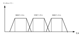
チャネル幅/密度が増加すると、チャネル内のデータ送信は、同一のファイバ上に配置された隣接チャネルからのチャネル間干渉に晒される。図1Dは、本明細書における説明のために基準として使用されるデータチャネルの典型的な受信信号のパワー分布を示す。図1Cに示す送信機での信号整形と形状は明らかに類似しているが、受信機で受信されるデータチャネルから離れたところでは、信号エネルギーが隣接チャネルに漏洩している。エネルギーの漏洩は主に、特定の隣接チャネルの超過帯域幅の領域に影響する。基準チャネル分布から離れた付随信号パワーは、基準チャネルに隣接するチャネルのバックグラウンドノイズの増加に寄与する。 As channel width/density increases, data transmission within a channel is subject to inter-channel interference from adjacent channels located on the same fiber. FIG. 1D shows a typical received signal power distribution for the data channel used as a reference for the description herein. Although the signal shaping and shape at the transmitter shown in FIG. 1C are clearly similar, away from the data channel received at the receiver, signal energy leaks into adjacent channels. Energy leakage primarily affects regions of excess bandwidth of a particular adjacent channel. Satellite signal power away from the reference channel distribution contributes to increased background noise in channels adjacent to the reference channel.
図1Aからよく分かるように、チャネル幅をガードバンドへ広げると、漏洩したチャネルパワーの分布がガードバンドで重なることになる。ガードバンドにおける超過帯域幅は受信機においてクロック回復に使用されるため、隣接チャネルから漏洩したスペクトルエネルギーは、抽出されたデータクロックの整合性に影響を与え、クロックジッタの増加として現れる。 As can be clearly seen from FIG. 1A, when the channel width is extended to the guardband, the leaked channel power distributions overlap in the guardband. Since the excess bandwidth in the guardband is used for clock recovery at the receiver, leaked spectral energy from adjacent channels affects the integrity of the extracted data clock and manifests itself as increased clock jitter.
通常、図1Bに示すように、ガードバンドは、チャネル間の干渉を制限するために、チャネルを分離すべく確保される。ガードバンドの確保は、相互運用性を得るための事業者間の合意に基づく場合がある。 Typically, guard bands are reserved to separate channels to limit inter-channel interference, as shown in FIG. 1B. Ensuring guard bands may be based on agreements between operators for interoperability.
データ転送の観点からは、図1Bに示すガードバンドは、各NMCの両端のデッドバンドである。ガードバンドは最大6.25GHzのロールオフをとることがあるため、貴重なスペクトルを占める。 From a data transfer perspective, the guard bands shown in FIG. 1B are dead bands across each NMC. The guard band can roll off up to 6.25 GHz and thus occupy valuable spectrum.
光通信システムの現在の実装では、パフォーマンス・メトリック(OSNRなど)は、ネットワークでセットアップされたデータチャネルから収集される。新しいデータチャネルがネットワークに追加されるに際し、ネットワーク管理プロセスにより、パフォーマンス・メトリックを利用してデータ転送容量の追加を最適化することが望まれる。特に、グリッドレス配置において、その主な目的は、チャネル密度を増加して、より多くのチャネルを同じCCバンドまたはC+Lバンドに収めることである。リンク条件に基づいてコヒーレント受信機設定を制御することによりチャネル密度を適応的に増加させることで、様々なスペクトル幅のNMC信号にトラフィックを割り当てる際の敏捷性の向上をもたらす。 In current implementations of optical communication systems, performance metrics (such as OSNR) are collected from data channels set up in the network. As new data channels are added to the network, it is desirable for the network management process to utilize performance metrics to optimize the addition of data transfer capacity. Especially in gridless deployment, the main purpose is to increase the channel density to fit more channels in the same CC band or C+L band. Adaptively increasing channel density by controlling coherent receiver settings based on link conditions provides increased agility in allocating traffic to NMC signals of varying spectral widths.
受信機におけるクロック回復の主な目的は、クロック信号のタイミングオフセットを推定し、該オフセットを補償することである。受信機のデータコンバータは、信号対ノイズ比(SNR)の低下に敏感である。良好なパフォーマンスを得るには、A/Dコンバータ(ADC)のクロックタイミングを高周波で最適化する必要がある。信号処理は、光チャネル干渉を補償するために使用される。 The main purpose of clock recovery in receivers is to estimate the timing offset of the clock signal and compensate for it. Receiver data converters are sensitive to signal-to-noise ratio (SNR) degradation. For good performance, the analog-to-digital converter (ADC) clock timing needs to be optimized at high frequencies. Signal processing is used to compensate for optical channel interference.
既知の受信機アーキテクチャは、通常、デジタルコンポーネントとアナログコンポーネントの組み合わせを使用する。典型的な設計は、フィードフォワードベース、フィードバックベース、または両方の組み合わせであってよい。図3を参照すると、光受信機でのクロック回復は、受信機で受信した送信機クロック信号に追従するように設定された比例/積分コントローラを介して受信機の電圧制御発振器(VCO)を直接制御することで実現される。 Known receiver architectures typically use a combination of digital and analog components. Typical designs may be feedforward-based, feedback-based, or a combination of both. Referring to FIG. 3, clock recovery in the optical receiver directly drives the receiver's voltage-controlled oscillator (VCO) through a proportional/integral controller that is set to track the transmitter clock signal received at the receiver. It is realized by controlling.
図3Bを参照すると、クロック回復ループは、デジタル処理ドメインに実装された位相検出器(PD)と、VCOゲインと、フィルタ要素とを中心に構築され、連携してノイズの発生源を削減する。例えば、送信機クロックは、超過帯域幅の信号エネルギーを使用して総位相ノイズを推定するゴダール(Godard)またはガードナー(Gardner)の早期-遅延エラーインジケータ抽出方法を使用して受信機で抽出され得る。その例は、F.M.Gardnerの「サンプル受信機用のBPSK/QPSKタイミングエラー検出器(A BPSK/QPSK timing-error detector for sampled receivers)」、IEEE Trans.Commun.、第34巻、第423~429頁、1986年5月に記載されている。信号エラーは、受信機のサンプリングクロックを調整する制御ループによって抑制される。 Referring to FIG. 3B, a clock recovery loop is built around a phase detector (PD) implemented in the digital processing domain, a VCO gain, and filter elements that work together to reduce sources of noise. For example, the transmitter clock can be extracted at the receiver using the Godard or Gardner early-delay error indicator extraction method, which estimates the total phase noise using excess bandwidth signal energy. . An example of this is F. M. Gardner, "A BPSK/QPSK timing-error detector for sampled receivers," IEEE Trans. Commun. 34, pp. 423-429, May 1986. Signal errors are suppressed by a control loop that adjusts the receiver's sampling clock.
クロックジッタは、受信機での高速ADCのサンプリングモーメントの不確実性の尺度である。クロックジッタは、抽出されたクロック信号の位相誤差の標準偏差に比例する。コヒーレント受信機は、光信号伝搬ジッタと受信機PLL実装固有ジッタの2つのジッタ発生源を許容しなければならない。
ジッタ(合計)=ジッタ(受信信号)+ジッタ(受信機) (2)
Clock jitter is a measure of the uncertainty of the sampling moment of a high speed ADC at the receiver. Clock jitter is proportional to the standard deviation of the phase error of the extracted clock signal. A coherent receiver must tolerate two sources of jitter: optical signal propagation jitter and receiver PLL implementation-specific jitter.
Jitter (total) = jitter (received signal) + jitter (receiver) (2)
光信号伝搬ジッタは、自然放射増幅光(ASE:Amplified Spontaneous Emission)、波長分散、カー(Kerr)の非線形性によるものである。自然放射増幅光は、光回線増幅器によって引き起こされる。タイミング情報をデジタル的に回復する前に、波長分散の大部分を受信機で補填する必要がある。特定の残留波長分散許容値が予想され、ペナルティが伴う。自己位相変調や相互位相変調などのカーの非線形性は、タイミングジッタに影響を与える。カーの非線形性に関する詳細は、M.Eiseltらの「WDMシステムにおけるXPMシステムペナルティへのタイミングジッタと振幅歪みの寄与(Contribution of timing jitter and to XPM system penalty in WDM systems)」、IEEE Photonics Technology Letters、第11巻第6号、第748~750頁、1999年6月、およびV.S.Grigoryanらの「線形化を使用した分散管理光ファイバ通信におけるタイミングと振幅ジッタの計算(Calculation of Timing and Amplitude Jitter in Dispersion-Managed Optical Fiber Communications Using Linearization)」、J.Lightwave Technol.第17巻、第1347頁~(1999)において記載されている。 Optical signal propagation jitter is due to amplified spontaneous emission (ASE), chromatic dispersion, and Kerr nonlinearity. Spontaneous emission amplified light is caused by an optical line amplifier. Most of the chromatic dispersion must be compensated at the receiver before the timing information can be recovered digitally. A certain residual chromatic dispersion tolerance is expected, with penalties involved. Kerr nonlinearities such as self-phase modulation and cross-phase modulation affect timing jitter. Further details on Kerr's nonlinearity can be found in M. Eiselt et al., "Contribution of timing jitter and to XPM system penalty in WDM systems," IEEE Photonics Technology Letters, Vol. 750, June 1999; S. Grigoryan et al., "Calculation of Timing and Amplitude Jitter in Dispersion-Managed Optical Fiber Communications Using Linearization," J. Am. Lightwave Technol. 17, pp. 1347-(1999).
送信機クロックと受信機クロックの双方における電子部品のうちジッタの主な発生源は、VCOとチャージポンプである。図3Cに示すように、VCOは、キャリア周波数に対して低い周波数オフセットで高い位相ノイズとして現れるジッタの累積の影響を受ける。 Among the electronic components in both the transmitter and receiver clocks, the major sources of jitter are the VCO and the charge pump. As shown in FIG. 3C, the VCO suffers from jitter accumulation that appears as high phase noise at low frequency offsets relative to the carrier frequency.
完璧な送信機を想定すると、受信機でのジッタの他の発生源は、クロックバッファの熱ノイズとフリッカノイズ、ADCの内部アパーチャ、電源変動および電磁結合である。後者は、複数の回路が同じ基板上で集積される場合に電子チャネル長が減少することによるものである。一部のジッタ、またはリップル効果は、受信機PLLの閉ループ制御によって引き起こされる。ループフィルタの次数と帯域幅の設計は、受信機で誘発される累積ジッタの制御において重要な役割を果たす。 Assuming a perfect transmitter, other sources of jitter at the receiver are clock buffer thermal and flicker noise, ADC internal aperture, power supply fluctuations and electromagnetic coupling. The latter is due to the reduction in electronic channel length when multiple circuits are integrated on the same substrate. Some jitter, or ripple effects, are caused by closed-loop control of the receiver PLL. The design of the loop filter order and bandwidth plays an important role in controlling the cumulative jitter induced in the receiver.
図2は、Tx信号位相ノイズ、RxVCOクロック位相ノイズおよびチャネル間隔に依存する隣接チャネル干渉に集約された、受信機で見られる様々な受信信号成分の位相ドメイン(ΦdBc)スペクトル密度(位相ノイズ)の変動を示す。有効なクロック回復帯域幅も、プログラム可能なクロック回復帯域幅として破線で示す。 Figure 2 shows the phase-domain (ΦdBc) spectral densities (phase noise) of the various received signal components seen at the receiver, summarized in Tx signal phase noise, RxVCO clock phase noise and channel spacing dependent adjacent channel interference. Show variation. The effective clock recovery bandwidth is also shown in dashed line as the programmable clock recovery bandwidth.
従来のクロック回復システムに関して、受信機のジッタは、受信機でのVCO位相ノイズ抑制と密接に結び付いている。これは、固有位相ノイズが大きい受信機VCOを使用した場合、(受信機で検知される)送信されたクロックのジッタを低下させることはほとんど意味がないことを意味する。これは、「Rx位相ノイズ」曲線の内側に「Tx位相ノイズ」曲線を示す図2において例示されている。逆に、Rx位相ノイズは、(破線の曲線で示されている受信機のクロック回復ループによって整形される)Tx位相ノイズと受信機の内部位相ノイズの合計である。クロック回復帯域幅を最適化して隣接チャネルからのエネルギー漏洩を抑制するには、受信機で適切な受信機VCO位相ノイズ抑制が必要である。図2では、これは、「Rx位相ノイズ」曲線がノイズ抑制を示す破線の曲線よりも下の部分を持つことによって示される。Rx位相ノイズ曲線の破線の曲線の外側の部分は、未追跡ジッタを強調するものである。 For conventional clock recovery systems, receiver jitter is closely tied to VCO phase noise suppression at the receiver. This means that it makes little sense to reduce the jitter of the transmitted clock (detected at the receiver) when using a receiver VCO with high intrinsic phase noise. This is illustrated in FIG. 2 which shows the 'Tx phase noise' curve inside the 'Rx phase noise' curve. Conversely, the Rx phase noise is the sum of the Tx phase noise (shaped by the receiver's clock recovery loop, shown by the dashed curve) and the receiver's internal phase noise. Adequate receiver VCO phase noise suppression at the receiver is required to optimize the clock recovery bandwidth and suppress energy leakage from adjacent channels. In FIG. 2 this is indicated by the "Rx phase noise" curve having a portion below the dashed curve indicating noise suppression. The portion of the Rx phase noise curve outside the dashed curve highlights the untracked jitter.
最終的に、データクロック信号の位相情報を識別できないと、受信機はクロック同期を取得できない結果となる。クロック同期の取得に失敗すると、データチャネルにおけるデータが回復不能となる。 Ultimately, the inability to discern the phase information of the data clock signal results in the receiver's inability to obtain clock synchronization. Failure to obtain clock synchronization will result in unrecoverable data on the data channel.
光グリッドレスネットワークのコンテキストでは、隣接チャネルからのクロストークは、線形ノイズ(障害)の追加的な発生源である。図2から、ガードバンドを減らすと、送信されたクロックの位相情報が隣接チャネル干渉の下に埋もれてしまう可能性があることが分かる。隣接するチャネルからのクロストークは、クロック回復が超過帯域幅に依存している場合、克服すべき大きな課題である。 In the context of optical gridless networks, crosstalk from adjacent channels is an additional source of linear noise (impairment). From FIG. 2, it can be seen that reducing the guardband can cause the phase information of the transmitted clock to be buried under adjacent channel interference. Crosstalk from adjacent channels is a major challenge to overcome when clock recovery relies on excess bandwidth.
光チャネル密度を増加しつつ、同期取得を改善する必要がある。 There is a need to improve synchronous acquisition while increasing optical channel density.
本明細書で提案される解決策は、データチャネル間のガード間隔を減らすことにより、より高いスペクトル効率を提供するシステム、回路および方法を提供する。これは、受信機のPLL帯域幅に影響を与えることなく、有効なクロック回復帯域幅を下げることで実現可能であることが見出された。 The solutions proposed herein provide systems, circuits and methods that provide higher spectral efficiency by reducing guard intervals between data channels. It has been found that this can be achieved by lowering the effective clock recovery bandwidth without affecting the PLL bandwidth of the receiver.
クロック回復に超過帯域幅を使用する受信機が、チャネル重複の量に基づいてクロック回復帯域での平均化を向上する技術と回路が提案される。これにより、隣接アクティブチャネルから対象アクティブチャネルに漏洩するスペクトルエネルギーの影響を緩和し、受信した送信クロックの位相推定の精度を向上させる。 Techniques and circuits are proposed for receivers that use excess bandwidth for clock recovery to improve averaging over the clock recovery band based on the amount of channel overlap. This mitigates the effect of spectral energy leaking from the adjacent active channel to the target active channel and improves the accuracy of phase estimation of the received transmit clock.
提案される解決策の一態様によれば、位相ロックループ回路とクロック回復ループ回路を備える光受信機が提供され、前記位相ロックループ回路は、受信機ローカル基準クロックによって生成された基準信号に基づいて、A/Dコンバータを介して受信信号のサンプリングのタイミングをとるためのサンプリング信号を提供する電圧制御発振器と、前記基準信号の信号変化を平滑化して、前記サンプリング信号の位相ノイズを低減するように構成されたローパスフィルタを備える。前記クロック回復ループ回路は、前記受信信号と前記サンプリング信号との間の位相差を示す第1の出力位相差信号を提供するデジタル位相検出器と、前記位相差信号をフィルタリングして、前記サンプリング信号のクロック回復帯域幅を設定するために使用される制御信号を提供するように構成されたデジタルコントローラを備える。 According to one aspect of the proposed solution, an optical receiver is provided comprising a phase-locked loop circuit and a clock recovery loop circuit, said phase-locked loop circuit being based on a reference signal generated by a receiver local reference clock. a voltage controlled oscillator for providing a sampling signal for timing sampling of a received signal via an A/D converter; and a low pass filter configured to: The clock recovery loop circuit includes a digital phase detector that provides a first output phase difference signal indicative of a phase difference between the received signal and the sampled signal; a digital controller configured to provide a control signal used to set the clock recovery bandwidth of the .
提案される解決策の別の態様によれば、光受信機において受信信号をサンプリングする方法が提供される。この方法は、データチャネル用の所要光信号対ノイズ比を取得することと、同じリンク上の複数のトランスポンダからクロック情報を取得して、前記所要光信号対ノイズ比に基づいてチャネルジッタを見いだすことと、クロック回復帯域幅パラメータとチャネルデータ帯域幅パラメータを決定することと、前記受信機の位相ロックループ回路内に、前記チャネルデータ帯域幅パラメータに基づいてローパスフィルタを構成することと、前記受信機の前記クロック回復ループ回路内に、前記クロック回復帯域幅パラメータに基づいてデジタルコントローラを構成することを含み、受信機電圧制御発振器におけるノイズを排除するための高帯域幅の要件は、クロック回復帯域幅要件から切り離されている。 According to another aspect of the proposed solution, a method is provided for sampling a received signal in an optical receiver. The method includes obtaining a desired optical signal-to-noise ratio for a data channel, obtaining clock information from multiple transponders on the same link, and finding channel jitter based on said desired optical signal-to-noise ratio. determining a clock recovery bandwidth parameter and a channel data bandwidth parameter; configuring a low pass filter within a phase-locked loop circuit of the receiver based on the channel data bandwidth parameter; A high bandwidth requirement to eliminate noise in a receiver voltage controlled oscillator includes configuring a digital controller based on the clock recovery bandwidth parameter within the clock recovery loop circuit of Separated from requirements.
提案される解決策の別の態様によれば、データチャネルをセットアップする構成された帯域幅使用コントローラが提供される。前記コントローラは、データチャネルのための所要光信号対ノイズ比を取得し、同じリンク上の複数のトランスポンダからクロック情報を取得して、前記所要光率に基づいてチャネルジッタを特定し、クロック回復帯域幅パラメータとチャネルデータ帯域幅パラメータとを決定し、受信機の位相ロックループ回路内に、前記チャネルデータ帯域パラメータに基づいてローパスフィルタを設定し、前記受信機のクロック回復ループ回路内に、前記クロック回復帯域幅パラメータに基づいてローパスフィルタを設定するように構成され、前記受信機の受信機電圧制御発振器におけるノイズを排除するための高帯域幅の要件は、クロック回復帯域幅要件から切り離されている。 According to another aspect of the proposed solution, a configured bandwidth usage controller for setting up data channels is provided. The controller obtains a desired optical signal-to-noise ratio for a data channel, obtains clock information from multiple transponders on the same link, determines channel jitter based on the desired optical rate, and clock recovery bandwidth. determining a width parameter and a channel data bandwidth parameter; setting a low pass filter in a phase locked loop circuit of a receiver based on the channel data bandwidth parameter; configured to set a low pass filter based on a recovery bandwidth parameter, wherein the high bandwidth requirement for rejecting noise in a receiver voltage controlled oscillator of said receiver is decoupled from the clock recovery bandwidth requirement. .
提案される解決策は、以下の添付の図面を参照した以下の本発明の実施形態の詳細な説明により、よりよく理解され得る。 The proposed solution can be better understood from the following detailed description of embodiments of the invention with reference to the accompanying drawings.
なお、図面全体を通して、類似の特徴には類似の参照符号が付される。 Similar features are provided with similar reference numerals throughout the drawings.
提案される解決策の動作原理は、プログラム可能なクロック回復帯域幅の選択を提供して、受信機VCOの位相ノイズ抑制パラメータの調整とは無関係に隣接チャネルの漏れを抑制する等するクロック回復回路の採用に基づく。その目的は、クロック回復帯域幅を最適化し、隣接チャネルの干渉を取り除くことである。 The operating principle of the proposed solution is a clock recovery circuit that provides programmable clock recovery bandwidth selection to suppress adjacent channel leakage independently of adjusting the phase noise suppression parameters of the receiver VCO, etc. Based on the adoption of The purpose is to optimize the clock recovery bandwidth and remove adjacent channel interference.
提案される解決策の一の実施形態によれば、受信機に備わるそのようなクロック回復回路400は、図4Aに示されるように、アナログPLLのフィードバック経路に位相回転子402を使用する。位相回転子402は、固有のVCOジッタ位相ノイズ抑制をクロック回復から切り離す。
According to one embodiment of the proposed solution, such a
アナログPLL404は、チャージポンプ412にトリガ信号410を提供するアナログ位相検出器408を使用してローカル基準クロック406にロックする。チャージポンプ412は、電圧設定信号414をローパスフィルタ416に提供する。ローパスフィルタ416は高帯域幅に設定され、電圧信号414の変動を平滑化し、VCO418の出力420におけるVCO位相ノイズを低減する。位相回転子ベースのクロック回復ループ424(デジタルPLL)は、アナログPLL404にネストされ、デジタル位相検出器428を用いて受信データ信号426にロックする。受信データ信号426は、送信クロック信号情報を含む。デジタル位相検出器428の出力430は、受信データ信号とVCO出力420との間の位相差を示しており、デジタルアキュムレータ432に提供される。デジタルアキュムレータ432によって出力されるデジタルコード434は、位相回転子402を、アナログPLLループ404におけるフィードバック信号を遅くしたり早めたりするように構成する。位相回転子402は、未追跡のRMSジッタの合計と比較すると、より細かい分解能を持ちうる。デジタルコードは、例えば関数依存性またはルックアップテーブルを介して、例えばアークタンジェントとI-Qの不一致による非線形エラーを補正するために使用される。回路400は、VCO418の位相ノイズを排除するアナログPLL404の高帯域幅の要件を、クロック回復帯域幅の要件から切り離すように構成される。位相回転子ベースのデジタルクロック回復帯域幅は、VCOジッタ生成に対する受信データ信号のジッタ除去を改善し、(デジタルアキュムレータ432を用いる)フィルタリング/平均化を通じてデジタル位相検出器エラーを最小限に抑える。回復されたデータクロック420を用いて、受信データ信号426をサンプリングするADCをトリガする。図4Aに示す構成により、高帯域幅のアナログPLL404を使用したVCO位相ノイズ抑制の最適化と、クロック回復帯域幅を最小限とすることによりクロック回復帯域への隣接チャネル漏洩の最適化が提供される。
提案される解決策の別の実施形態によれば、図4Bに示されるように、クロック回復帯域幅を低減して隣接チャネル干渉を除去する別の技法は、例えば、受信機の基準クロックを調整することができる。回路500では、VCO418の出力520から導出されたアナログPLLフィードバック信号が、510において、調整可能な基準クロック506の出力と組み合わされる。組み合わせ信号512は、駆動信号512の変動を平滑化して、VCO418の出力520におけるVCO位相ノイズを低減する高帯域幅に設定されたローパスフィルタ416によってフィルタリングされる。分周器514は、アナログPLLループ504のフィードバック信号を提供する。第2のデジタルPLLループ524は、デジタル位相検出器428を使用して、送信クロック情報426を含む受信データ信号をVCO出力520と比較する。デジタル位相検出器428の出力430は、データ信号とVCO出力420との間の位相差を示し、デジタルコントローラ532に提供される。デジタルコントローラ532の出力536を用いて、調整可能な基準クロック506のデジタルPLL周波数制御が行われる。デジタルコントローラ532のデジタルコードは、調整可能な基準クロック502を、より低いまたは高い周波数が出力されて、アナログPLLループ504を駆動するように構成する。デジタルコードは、例えば関数依存性またはルックアップテーブルを通じて、例えばアークタンジェントとI-Qの不一致による非線形エラーを補正するために使用される。このように、調整可能な基準クロックは、周波数制御ワード536が制御ブロック532によって提供される数値制御発振器(NCO:Numerically Controlled Oscillator)と見なすことができる。ここでも、この構成により、高帯域幅のアナログPLL404を使用したVCO位相ノイズ抑制の最適化と、クロック回復ループ524の帯域幅を最小限とすることによりクロック回復帯域への隣接チャネル漏洩の最適化が提供される。
According to another embodiment of the proposed solution, as shown in FIG. 4B, another technique for reducing the clock recovery bandwidth and removing adjacent channel interference is to adjust the receiver's reference clock, for example. can do. In
図4Aおよび図4Bには別個の回路が示されているが、ハイブリッド回路も機能することを理解されたい。 Although separate circuits are shown in FIGS. 4A and 4B, it should be understood that hybrid circuits would also work.
なお、SNRを測定する際にノイズがゼロ平均と無相関であると仮定すると、N個の観測値を平均すると、その結果は平滑化される。

図2を参照すると、クロック回復帯域幅を低くすると、隣接チャネル干渉の影響の排除に効果的に寄与し、受信機での送信機クロックの抽出に対する信号の整合性の向上をもたらす。また、このようなシステムは、クロック回復帯域幅を低くすると受信機の送信クロック追跡(トラッキング)能力が制限されるため、送信機ジッタを確実に低くする信号送信技術を必要とする。 Referring to FIG. 2, a lower clock recovery bandwidth effectively contributes to eliminating the effects of adjacent channel interference, resulting in improved signal integrity for transmitter clock extraction at the receiver. Such systems also require signal transmission techniques that ensure low transmitter jitter, since low clock recovery bandwidth limits the receiver's transmit clock tracking ability.
更に、クロック回復帯域幅を低くすると、受信機による他のジッタ源の効果的な追跡が低下する。Jrx(受信機により引き起こされるジッタ)が受信機PLLによって追跡されると仮定すると、Jchannelは同じNMC内の隣接チャネルから推定できる。全位相エラー(Jtx)における送信機クロックの標準偏差が低い場合、最適化されたパラメータ(帯域幅とゲイン)は、最適なチャネル間隔を抽出するフィッティングを実行するための仕様に基づくことができる。これは、以下のようにまとめることができる。
Jinterference(間隔)<Jspec-Jchannel-Jtx-Jrx
Furthermore, lowering the clock recovery bandwidth reduces the effective tracking of other jitter sources by the receiver. Assuming J rx (receiver-induced jitter) is tracked by the receiver PLL, J channel can be estimated from adjacent channels within the same NMC. If the transmitter clock standard deviation in total phase error (J tx ) is low, the optimized parameters (bandwidth and gain) can be based on the specification to perform the fitting to extract the optimal channel spacing. . This can be summarized as follows.
Jinterference < Jspec - Jchannel - Jtx - Jrx
対象のチャネルの有効なクロック回復帯域幅とゲインをプログラミングするために、隣接チャネルによって引き起こされる位相ノイズを考慮するプロセスが提案される。このようなプロセスを図5Aに示す。このプロセスでは、光ネットワークのタイプに基づいて、帯域幅使用の増加に対するシステムペナルティの評価が可能である。この方法論を使用して、例えばチャネル間隔を推定することにより、所与のチャネル容量に必要とされる所要光信号対ノイズ比(ROSNR)を求めることができる。プロセス600は新しいチャネルの要求に伴い開始され(602)、光ネットワークタイプの決定を伴う(604)。固定グリッド光システムの場合、所定の受信機設定を使用して、チャネル幅の増加を可能にするように、クロック回復帯域幅、ゲイン、ビットエラーレート(BER)、および、隣接チャネル減衰の低減が選択される(606)。ただし、604でネットワーク配置にグリッドレス光システムが含まれる場合、総当たり(ブルートフォース)検索方法を使用して、事前定義された公称間隔のチャネルまたは(1+β)*ボーレートのチャネルを追加することにより、パラメータを最適する。典型的なグリッドレス配置には、ROADMの粒度、例えば、12.5GHzの整数倍に基づくチャネル間隔が含まれる。
In order to program the effective clock recovery bandwidth and gain of the channel of interest, a process is proposed that takes into account the phase noise induced by adjacent channels. Such a process is illustrated in FIG. 5A. This process allows an evaluation of the system penalty for increased bandwidth usage based on the type of optical network. This methodology can be used to determine the required optical signal-to-noise ratio (ROSNR) required for a given channel capacity, eg, by estimating the channel spacing.
市販のコヒーレントモデムで通常使用される様々な変調形式のためのROSNRに対するチャネル密度の影響が測定され、間隔とOSNRの利用可能性によりジッタがどのように影響を受けるかに関するガイドラインが提供される。隣接チャネルからの漏洩エネルギーは、対象のチャネルに付加されたノイズの形として現れる。そのため、前方誤り訂正(FEC:Forward Error Collection)しきい値を満たすROSNRは増加する。図5Bは、チャネル密度の増加に必要とされる最小の利用可能ROSNRを求めるための、様々な変調形式のシミュレートされたペナルティを示す。海底リンク、長距離、メトロ、およびデータセンターの相互接続をカバーする配置が調査され、リンクバジェットにおけるROSNRがチャネル間隔によってどのように影響を受けるかを予測可能となった。 The effect of channel density on ROSNR for various modulation formats commonly used in commercial coherent modems is measured to provide guidelines on how jitter is affected by spacing and OSNR availability. Leakage energy from adjacent channels appears as a form of noise added to the channel of interest. Therefore, the ROSNR that satisfies the Forward Error Correction (FEC) threshold increases. FIG. 5B shows simulated penalties for various modulation formats to find the minimum available ROSNR required for increased channel density. Deployments covering submarine links, long haul, metro and data center interconnects have been investigated to predict how ROSNR in link budget is affected by channel spacing.
測定のグラフから、ペナルティは採用されたコンスタレーションの密度に伴い増加する。図5Aに示すプロセスに戻ると、利用可能なOSNRマージンがない場合(610)、プロセスは、ITU-T G.870に準拠する所定のパラメータを使用してステップ606から再開する。しかしながら、OSNRマージンが利用可能である場合、クロック情報は、グリッドレス光システムにおいて、通常、同じリンク上のトランスポンダから取得され得る(612)。 From the measurement graph, the penalty increases with the density of the adopted constellation. Returning to the process shown in FIG. 5A, if there is no OSNR margin available (610), the process follows ITU-T G. Resume from step 606 using the predetermined parameters according to G.870. However, if OSNR margin is available, clock information can be obtained 612 from transponders on the same link, typically in gridless optical systems.
受信機PLL内のVCOの発生した位相ノイズのパワースペクトル分布(PSD)は、チャネル密度とOSNRとをジッタマージンに関連付けるローレンツ(Lorentzian)分布としてモデル化することができる。上記のノイズ源成分の線形効果は、シミュレーションにおいて組み合わせることができ、その結果を図5Cに示す。マージン0%は、受信機が送信機クロックに同期できず、受信機が定常状態に到達できないポイントである。図5Cは、ジッタ推定において誘発された高帯域幅位相ノイズに起因するASEノイズレベルの変化(グラフの左側)と比較して急勾配な、チャネル間隔に対する変動(グラフの右側)を示す。これを念頭に置いて、図5Aに戻り、受信機のファームウェア(または制御プロセッサ)を使用して2Dスイープを実行して(612)、利用可能なマージンに基づいて図5Cに示す変動にフィッティングすることにより最適化されたジッタを求める。最適化プロセスにより、(未追跡ジッタと光非線形効果をカバーするための)既存のチャネル情報と(線形クロストークペナルティに対処するための)OSNRマージンに関して、最適なクロック回復パラメータ(クロック回復帯域幅)で受信機を操作するためのスイート・スポットを特定する(614)。離散ルックアップテーブルまたは連続フィッティングの両方を使用して、(送受信機に関連する仕様に基づいて定義された)ジッタマージンを既知のOSNR用のチャネル間隔へと変換する。別の言い方をすると、ジッタマージンを隣接チャネルから推定する際に、図5Cの変動を用いてチャネル間隔が規定される。推定ジッタマージンには、非線形の影響が含まれる。フィッティングを用いて、マージン付きチャネル間隔が予測される。 The power spectral distribution (PSD) of the VCO generated phase noise in the receiver PLL can be modeled as a Lorentzian distribution that relates channel density and OSNR to jitter margin. The linear effects of the above noise source components can be combined in a simulation and the results are shown in FIG. 5C. A margin of 0% is the point at which the receiver cannot synchronize to the transmitter clock and the receiver cannot reach steady state. FIG. 5C shows a steeper variation versus channel spacing (right side of the graph) compared to the change in ASE noise level (left side of the graph) due to high-bandwidth phase noise induced in the jitter estimation. With this in mind, returning to FIG. 5A, a 2D sweep is performed (612) using the receiver's firmware (or control processor) to fit the variation shown in FIG. 5C based on the available margin. to find the optimized jitter. The optimization process determines the optimal clock recovery parameter (clock recovery bandwidth) in terms of existing channel information (to cover untracked jitter and optical nonlinear effects) and OSNR margin (to address linear crosstalk penalty) A sweet spot for operating the receiver is identified (614). Both discrete lookup tables or continuous fitting are used to convert the jitter margin (defined based on specifications associated with the transceiver) into channel spacing for known OSNR. Stated another way, the variation of FIG. 5C is used to define channel spacing when estimating jitter margin from adjacent channels. The estimated jitter margin includes non-linear effects. Using fitting, margined channel spacing is predicted.
グリッドレス配置では、所与のOSNR目標のためにチャネル間隔を最適化してチャネル間隔を絞るように、受信機でクロック回復帯域幅を設定することができる(616)。図4Aおよび図4Bを参照して、クロック回復帯域幅は、ローパスフィルタ416のパラメータを調整することにより設定される。チャネル間隔は、デジタルアキュムレータ432またはコントローラ532のパラメータを指定することで設定できる。
In a gridless deployment, the clock recovery bandwidth can be set 616 at the receiver to optimize the channel spacing and narrow the channel spacing for a given OSNR target. 4A and 4B, the clock recovery bandwidth is set by adjusting the parameters of
図5Aに示すプロセスは、これらに限定されないが、受信機コントローラ、ラインカードコントローラ、ネットワークノードコントローラ、リンクコントローラ、コントロールプレーンコントローラ、光システムコントローラ、集中型ネットワークコントローラなどの帯域幅使用コントローラにより、これらに限定されないが、ファームウェア、ソフトウェア、ステートマシンロジックなどのコード化ロジックを介して実装される。 The process illustrated in FIG. 5A is implemented by bandwidth usage controllers such as, but not limited to, receiver controllers, line card controllers, network node controllers, link controllers, control plane controllers, optical system controllers, centralized network controllers. Implemented via coded logic such as, but not limited to, firmware, software, state machine logic.
図5Aに示す方法の有効性を実証するために、グリッドレス実験設定を採用した。実験設定では、ファイバの伝搬効果を考慮し、図6Aに示すように制御された障害を導入して、効果を定量的に評価した。実験では、提案された最適化が現実のシナリオで安定することを確認するために、受信機(Wavelogicモデム)に対し意図的にストレスを与えた。Ciena6500のROADMを使用した配置で通常採用されているグリッドレス設定を使用して、複数のチャネルを1つの光ファイバ上で併用した。対象のプローブ波長を選択し、プログラム可能な波長(調整可能なレーザー)を有するコヒーレント送受信機を使用してチャネル間隔を変更した。3つのチャネルをアクティブとし、中央の1つのチャネルをプローブとして用い、他の2つのチャネルを干渉源として用いた。3つのWaveLogic3トランスポンダ(100G/150G/200G)を使用して、35GBaudでの動作が提供された。実際のファイバ伝搬の模倣に役立てるために、偏波依存損失エミュレーター(PDL)と微分群遅延エミュレーター(DGD)を使用した。可変光減衰器(VOA)を使用して、ASEアンプにより提供されるノイズ障害の量を制御した。ファイバスプールは数キロメートルとした(ただし、リンクバジェットが順守される限り、どのような長さでもよい)。送信された偏波を混合するために、偏波スクランブラPC1、PC2を採用した。測定スイープは、偏波依存損失(PDL)、微分群遅延(DGD)、偏波状態率(PC1/PC2)およびOSNRの複数の値にわたって実行した。
A gridless experimental setup was employed to demonstrate the effectiveness of the method shown in FIG. 5A. In our experimental setup, we considered the propagation effects of the fiber and introduced a controlled impairment as shown in Fig. 6A to evaluate the effects quantitatively. In experiments, the receiver (Wavelogic modem) was deliberately stressed to confirm that the proposed optimization is stable in real-life scenarios. Multiple channels were combined on one optical fiber using a gridless setup typically employed in
図6Bは、テストしたチャネルの測定パワー分布を示す。通常の使用中には、隣接チャネルは同様のパワーを有する。パワーのより高い隣接チャネルの採用を、受信機にストレスを与えるために用いた。テスト方法は、あらゆるタイプの隣接チャネルに対しても一般化が可能である。 FIG. 6B shows the measured power distribution of the tested channel. During normal use, adjacent channels have similar powers. Employing higher power adjacent channels was used to stress the receiver. The test method can be generalized to any type of adjacent channel.
複数のチャネルを超ナイキストモードの動作に絞ろうとすると、ホワイトノイズのように見える線形クロストークからのペナルティが明らかである。提案された方法は、受信機がトラフィックを運ぶことができる境界を押し上げることを可能にした。図6Cおよび図6Dに示すように、この設定により、非最適な方法と同じ2dBのOSNRペナルティで1GHz少ない間隔でエラーなしで動作可能とした。この実験は、各NMCの光スペクトルにおいて、約10~20GHzを節約できることを示す。 When trying to squeeze multiple channels into a super-Nyquist mode of operation, the penalty from linear crosstalk that looks like white noise is evident. The proposed method allowed us to push the boundaries on which receivers can carry traffic. As shown in FIGS. 6C and 6D, this setup allowed error-free operation at 1 GHz less spacing with the same OSNR penalty of 2 dB as the non-optimal method. This experiment shows that about 10-20 GHz can be saved in the optical spectrum of each NMC.
このようなクロック回復方式は、例えば海底での適用などの狭間隔の適用において必要とされた場合にアナログ・フロント・エンドの厳密なフィルタリング要件を緩和するのに役立つことが分かった。 Such a clock recovery scheme has been found to help relax the stringent filtering requirements of the analog front end when required in closely spaced applications, such as undersea applications.
提案された解法をグリッドレス配置でのチャネル密度の増加に関して詳細に説明したが、図4Aおよび図4Bに示す同じ回路を使用して、固定グリッド配置においてチャネル幅を拡大することも可能である。固定グリッド配置では、より高いボーレートでビットエラーレート(BER)の増加が許容され、その際には、受信機において波長選択スイッチ(WSS)(図示しない)などの光フィルタリング装置によって対応するプログラム可能な隣接チャネル減衰がより低い状態で実施される(606)。 Although the proposed solution has been described in detail with respect to increasing channel density in gridless layouts, it is also possible to expand channel widths in fixed grid layouts using the same circuits shown in FIGS. 4A and 4B. A fixed grid arrangement allows an increase in bit error rate (BER) at higher baud rates, with a corresponding programmable Adjacent channel attenuation is performed with lower (606).
本発明をその好ましい実施形態を参照して図示し説明したが、当業者には、添付の請求項に規定される本発明の趣旨および範囲から逸脱することなく、形態および詳細に様々な変更を加えることができることが理解されよう。
Although the present invention has been illustrated and described with reference to preferred embodiments thereof, it will occur to those skilled in the art that various changes in form and detail may be made without departing from the spirit and scope of the invention as defined in the appended claims. It will be appreciated that it is possible to add
Claims (12)
受信信号と前記サンプリング信号との間の位相差を決定し、その位相差に基づいて制御信号を決定し、その制御信号を利用して前記位相ロックループ回路のクロック回復帯域幅を設定するように構成されたクロック回復回路とを有し、
前記クロック回復帯域幅は、隣接するチャネル干渉をフィルタリングにより除去するように最小化され、
前記クロック回復帯域幅は、所定の光信号対ノイズ比に対して受信チャネルのチャネル間隔を最適化するように設定されている、
フレキシブルグリッド光受信回路。 A phase-locked loop circuit configured to receive a reference clock and output a sampling signal generated by combining the output of the phase-locked loop circuit after phase noise reduction with the received reference clock. a phase-locked loop circuit;
determining a phase difference between a received signal and the sampled signal; determining a control signal based on the phase difference; and utilizing the control signal to set a clock recovery bandwidth of the phase locked loop circuit. a clock recovery circuit;
the clock recovery bandwidth is minimized to filter out adjacent channel interference;
wherein the clock recovery bandwidth is set to optimize channel spacing of receive channels for a given optical signal-to-noise ratio;
Flexible grid optical receiving circuit.
前記1つまたは複数のフレキシブルグリッドモデムに通信可能に結合され、以下のように構成された帯域幅使用コントローラとを有し、
前記帯域幅使用コントローラは、
前記1つまたは複数のフレキシブルグリッドモデム上の新規チャネルに対する所定の光信号対ノイズ比目標に対して、前記新規チャネルに必要な光信号対ノイズ比を決定し、
前記1つまたは複数のフレキシブルグリッドモデムに関連する隣接チャネルから推定されたジッタマージンを取得し、
前記推定されたジッタマージンを、前記所定の光信号対ノイズ比目標に基づいて、新規チャネルのチャネル間隔に変換するように構成されている、
フレキシブルグリッド光学システム。 one or more flexible grid modems comprising a flexible grid optical receiving circuit according to any one of claims 1 to 6 ;
a bandwidth usage controller communicatively coupled to the one or more flexible grid modems and configured to:
The bandwidth usage controller comprises:
determining a required optical signal-to-noise ratio for the new channel for a given optical signal-to-noise ratio target for the new channel on the one or more flexible grid modems;
obtaining estimated jitter margins from adjacent channels associated with the one or more flexible grid modems;
configured to convert the estimated jitter margin to channel spacing for a new channel based on the predetermined optical signal-to-noise ratio target;
Flexible grid optical system.
前記1つまたは複数のフレキシブルグリッドモデム上の新規チャネルに対する所定の光信号対ノイズ比目標に対して、前記新規チャネルに必要な光信号対ノイズ比を決定し、
前記1つまたは複数のフレキシブルグリッドモデムに関連する隣接チャネルから推定されたジッタマージンを取得し、
前記推定されたジッタマージンを、前記所定の光信号対ノイズ比目標に基づいて、新規チャネルのチャネル間隔に変換する、
方法。 Using one or more flexible grid modems comprising the flexible grid optical receiving circuit according to any one of claims 1 to 6 ,
determining a required optical signal-to-noise ratio for the new channel for a given optical signal-to-noise ratio target for the new channel on the one or more flexible grid modems;
obtaining estimated jitter margins from adjacent channels associated with the one or more flexible grid modems;
converting the estimated jitter margin to a channel spacing for a new channel based on the predetermined optical signal-to-noise ratio target;
Method.
Applications Claiming Priority (3)
| Application Number | Priority Date | Filing Date | Title |
|---|---|---|---|
| US15/795,676 | 2017-10-27 | ||
| US15/795,676 US10243671B1 (en) | 2017-10-27 | 2017-10-27 | Clock recovery circuits, systems and implementation for increased optical channel density |
| PCT/US2018/056851 WO2019083878A1 (en) | 2017-10-27 | 2018-10-22 | Clock recovery circuits, systems and implementation for increased optical channel density |
Publications (3)
| Publication Number | Publication Date |
|---|---|
| JP2021501516A JP2021501516A (en) | 2021-01-14 |
| JP2021501516A5 JP2021501516A5 (en) | 2021-10-07 |
| JP7244508B2 true JP7244508B2 (en) | 2023-03-22 |
Family
ID=64316986
Family Applications (1)
| Application Number | Title | Priority Date | Filing Date |
|---|---|---|---|
| JP2020523248A Active JP7244508B2 (en) | 2017-10-27 | 2018-10-22 | Clock recovery circuits, systems and implementations for increased optical channel density |
Country Status (4)
| Country | Link |
|---|---|
| US (2) | US10243671B1 (en) |
| EP (1) | EP3701645A1 (en) |
| JP (1) | JP7244508B2 (en) |
| WO (1) | WO2019083878A1 (en) |
Families Citing this family (11)
| Publication number | Priority date | Publication date | Assignee | Title |
|---|---|---|---|---|
| US10805064B1 (en) | 2019-04-23 | 2020-10-13 | Ciena Corporation | Built-in jitter loading and state of polarization generation to characterize optical transceivers |
| US10715169B1 (en) | 2019-05-21 | 2020-07-14 | Ciena Corporation | Coarse-fine gain-tracking loop and method of operating |
| US11228403B2 (en) * | 2019-12-09 | 2022-01-18 | Skyworks Solutions, Inc. | Jitter self-test using timestamps |
| CN111092714B (en) * | 2019-12-10 | 2022-05-06 | 中国科学院微电子研究所 | High-speed signal clock recovery method and device |
| US11119854B2 (en) * | 2020-02-14 | 2021-09-14 | Elite Semiconductor Memory Technology Inc. | Method of controlling verification operations for error correction of non-volatile memory device, and non-volatile memory device |
| US10985900B1 (en) | 2020-03-03 | 2021-04-20 | Ciena Corporation | Estimating clock phase error based on channel conditions |
| US11381306B2 (en) * | 2020-04-29 | 2022-07-05 | Cisco Technology, Inc. | Bisection searching algorithm to derive optimum baud rate with maximum spectral efficiency exploiting Q-margin-to-SNR-margin conversion |
| US11558061B2 (en) | 2021-04-22 | 2023-01-17 | Ciena Corporation | ADC self-calibration with on-chip circuit and method |
| US11463093B1 (en) | 2021-05-12 | 2022-10-04 | Ciena Corporation | Reducing non-linearities of a phase rotator |
| US11750287B2 (en) | 2021-05-25 | 2023-09-05 | Ciena Corporation | Optical DSP operating at half-baud rate with full data rate converters |
| US11770203B2 (en) * | 2021-09-09 | 2023-09-26 | Ciena Corporation | Matching transmitters with receivers for making network-level assignments |
Citations (2)
| Publication number | Priority date | Publication date | Assignee | Title |
|---|---|---|---|---|
| JP2008535387A (en) | 2005-03-30 | 2008-08-28 | シリコン・ラボラトリーズ・インコーポレイテッド | Data cleaning using asynchronous reference clock |
| JP2016521027A (en) | 2013-03-30 | 2016-07-14 | ゼットティーイー コーポレーションZte Corporation | Data recovery from quadrature phase shift keying modulated optical signals |
Family Cites Families (18)
| Publication number | Priority date | Publication date | Assignee | Title |
|---|---|---|---|---|
| JP4454798B2 (en) * | 2000-06-09 | 2010-04-21 | Necエレクトロニクス株式会社 | Clock regenerator |
| US20060024062A1 (en) | 2004-07-28 | 2006-02-02 | Nortel Networks Limited | Pre-compensation for modulator distortion in optical systems |
| US7492849B2 (en) * | 2005-05-10 | 2009-02-17 | Ftd Solutions Pte., Ltd. | Single-VCO CDR for TMDS data at gigabit rate |
| US7492195B1 (en) * | 2005-06-22 | 2009-02-17 | Cypress Semiconductor Corp. | Agile, low phase noise clock synthesizer and jitter attenuator |
| US7742507B1 (en) | 2006-03-28 | 2010-06-22 | Nortel Networks Limited | Method and system for phase and byte alignment on a multiplexed high speed bus |
| US20080240230A1 (en) * | 2007-03-29 | 2008-10-02 | Horizon Semiconductors Ltd. | Media processor with an integrated TV receiver |
| US8849882B2 (en) | 2007-10-19 | 2014-09-30 | The Royal Institution for the Association of Learning | Generation of an analog Gaussian noise signal having predetermined characteristics |
| US8855215B2 (en) | 2011-05-09 | 2014-10-07 | The Royal Institution For The Advancement Of Learning/Mcgill University | Phase/frequency synthesis using periodic sigma-delta modulated bit-stream techniques |
| US8497716B2 (en) * | 2011-08-05 | 2013-07-30 | Qualcomm Incorporated | Phase locked loop with phase correction in the feedback loop |
| US8384452B1 (en) * | 2011-09-13 | 2013-02-26 | Cortina Systems, Inc. | Integrated jitter compliant low bandwidth phase locked loops |
| US8786337B2 (en) * | 2012-05-14 | 2014-07-22 | Ensphere Solutions, Inc. | Low jitter clock generator for multiple lanes high speed data transmitter |
| US9037104B2 (en) * | 2013-02-04 | 2015-05-19 | Qualcomm, Incorporated | Receiver that reconfigures between zero intermediate frequency and direct sampling based on channel conditions |
| US9225430B2 (en) | 2013-05-20 | 2015-12-29 | Ciena Corporation | Digital noise loading for optical receivers |
| US9537493B2 (en) * | 2014-05-21 | 2017-01-03 | Robert Bosch Gmbh | Phase lock loop circuit having a wide bandwidth |
| US9634826B1 (en) * | 2015-11-30 | 2017-04-25 | Intel Corporation | Apparatus and method for automatic bandwidth calibration for phase locked loop |
| US9787466B2 (en) | 2016-03-09 | 2017-10-10 | Ciena Corporation | High order hybrid phase locked loop with digital scheme for jitter suppression |
| EP3602845B1 (en) * | 2017-03-21 | 2021-09-22 | Bifrost Communications APS | Optical communication systems, devices, and methods including high performance optical receivers |
| US10063367B1 (en) * | 2017-04-28 | 2018-08-28 | Ciena Corporation | Optical clock recovery using feedback phase rotator with non-linear compensation |
-
2017
- 2017-10-27 US US15/795,676 patent/US10243671B1/en active Active
-
2018
- 2018-10-22 EP EP18803818.6A patent/EP3701645A1/en active Pending
- 2018-10-22 JP JP2020523248A patent/JP7244508B2/en active Active
- 2018-10-22 WO PCT/US2018/056851 patent/WO2019083878A1/en unknown
-
2019
- 2019-02-07 US US16/270,203 patent/US10855380B2/en active Active
Patent Citations (2)
| Publication number | Priority date | Publication date | Assignee | Title |
|---|---|---|---|---|
| JP2008535387A (en) | 2005-03-30 | 2008-08-28 | シリコン・ラボラトリーズ・インコーポレイテッド | Data cleaning using asynchronous reference clock |
| JP2016521027A (en) | 2013-03-30 | 2016-07-14 | ゼットティーイー コーポレーションZte Corporation | Data recovery from quadrature phase shift keying modulated optical signals |
Also Published As
| Publication number | Publication date |
|---|---|
| US20190190617A1 (en) | 2019-06-20 |
| JP2021501516A (en) | 2021-01-14 |
| US10243671B1 (en) | 2019-03-26 |
| US10855380B2 (en) | 2020-12-01 |
| EP3701645A1 (en) | 2020-09-02 |
| WO2019083878A1 (en) | 2019-05-02 |
Similar Documents
| Publication | Publication Date | Title |
|---|---|---|
| JP7244508B2 (en) | Clock recovery circuits, systems and implementations for increased optical channel density | |
| US10944478B2 (en) | Fiber communication systems and methods | |
| US9831947B2 (en) | Margin determination systems and methods in optical networks | |
| US9698905B2 (en) | Optical transmission system, optical transmission apparatus and wavelength spacing measurement apparatus | |
| US9831976B2 (en) | Optical transmission apparatus, optical transmission system, and transmission wavelength control method | |
| Cugini et al. | Push-pull defragmentation without traffic disruption in flexible grid optical networks | |
| US8855498B2 (en) | Skew suppression method and optical transmission system | |
| KR101605683B1 (en) | Coherent transponder with enhanced frequency locking | |
| Fice et al. | Homodyne coherent optical receiver using an optical injection phase-lock loop | |
| US9325424B2 (en) | Optical phase compensation device, optical receiver, and optical phase compensation method | |
| US9800326B2 (en) | Optical transmission device and protection wavelength selection method | |
| US20070196111A1 (en) | Optic fiber network communication system with duobinary transceiver | |
| Al-Qadi et al. | Phase noise measurements and performance of lasers with non-white FM noise for use in digital coherent optical systems | |
| US20170019203A1 (en) | Optical receiver and method for updating tap coefficient of digital filter | |
| Foggi et al. | Signal overlap for elastic optical networks | |
| US11303381B2 (en) | Processing parameter and resource sharing architecture for superchannel based transmission systems | |
| Cugini et al. | Signal overlap for efficient 1+ 1 protection in elastic optical networks (EONs) | |
| Deynu et al. | Phase noise effects on the performance of joint carrier phase recovery algorithms in phase-locked WDM superchannel transmission systems | |
| Deynu et al. | Design of feedforward master–slave carrier phase recovery in frequency comb-based superchannel coherent transmission systems with nonlinear phase noise | |
| Perelló et al. | Reducing the number of transceivers with probabilistic constellation shaping in flex-grid over MCF optical backbone networks | |
| Lau et al. | Beyond 100 Gb/s: Advanced DSP techniques enabling high spectral efficiency and flexible optical communications | |
| Ranzini et al. | Local and remote laser frequency control in point-to-multipoint networks using digital subcarriers | |
| Fabrega et al. | Constant envelope coherent optical OFDM transceiver for elastic upgrade of transport network | |
| Fàbrega et al. | Experimental demonstration of heterodyne phase-locked loop for optical homodyne PSK receivers in PONs | |
| Silva et al. | Impact and compensation techniques of laser phase noise in ultra-dense coherent access networks |
Legal Events
| Date | Code | Title | Description |
|---|---|---|---|
| RD03 | Notification of appointment of power of attorney |
Free format text: JAPANESE INTERMEDIATE CODE: A7423 Effective date: 20210727 |
|
| RD04 | Notification of resignation of power of attorney |
Free format text: JAPANESE INTERMEDIATE CODE: A7424 Effective date: 20210729 |
|
| A521 | Request for written amendment filed |
Free format text: JAPANESE INTERMEDIATE CODE: A523 Effective date: 20210802 |
|
| A621 | Written request for application examination |
Free format text: JAPANESE INTERMEDIATE CODE: A621 Effective date: 20210802 |
|
| A977 | Report on retrieval |
Free format text: JAPANESE INTERMEDIATE CODE: A971007 Effective date: 20220906 |
|
| A131 | Notification of reasons for refusal |
Free format text: JAPANESE INTERMEDIATE CODE: A131 Effective date: 20220913 |
|
| A521 | Request for written amendment filed |
Free format text: JAPANESE INTERMEDIATE CODE: A523 Effective date: 20221213 |
|
| TRDD | Decision of grant or rejection written | ||
| A01 | Written decision to grant a patent or to grant a registration (utility model) |
Free format text: JAPANESE INTERMEDIATE CODE: A01 Effective date: 20230307 |
|
| A61 | First payment of annual fees (during grant procedure) |
Free format text: JAPANESE INTERMEDIATE CODE: A61 Effective date: 20230309 |
|
| R150 | Certificate of patent or registration of utility model |
Ref document number: 7244508 Country of ref document: JP Free format text: JAPANESE INTERMEDIATE CODE: R150 |