JP7241663B2 - Information processing device, information processing method, information processing program, and semiconductor manufacturing device - Google Patents
Information processing device, information processing method, information processing program, and semiconductor manufacturing device Download PDFInfo
- Publication number
- JP7241663B2 JP7241663B2 JP2019200139A JP2019200139A JP7241663B2 JP 7241663 B2 JP7241663 B2 JP 7241663B2 JP 2019200139 A JP2019200139 A JP 2019200139A JP 2019200139 A JP2019200139 A JP 2019200139A JP 7241663 B2 JP7241663 B2 JP 7241663B2
- Authority
- JP
- Japan
- Prior art keywords
- film thickness
- refractive index
- model
- information processing
- wafer
- Prior art date
- Legal status (The legal status is an assumption and is not a legal conclusion. Google has not performed a legal analysis and makes no representation as to the accuracy of the status listed.)
- Active
Links
Images


Classifications
-
- H—ELECTRICITY
- H01—ELECTRIC ELEMENTS
- H01J—ELECTRIC DISCHARGE TUBES OR DISCHARGE LAMPS
- H01J37/00—Discharge tubes with provision for introducing objects or material to be exposed to the discharge, e.g. for the purpose of examination or processing thereof
- H01J37/32—Gas-filled discharge tubes
- H01J37/32917—Plasma diagnostics
- H01J37/32926—Software, data control or modelling
-
- C—CHEMISTRY; METALLURGY
- C23—COATING METALLIC MATERIAL; COATING MATERIAL WITH METALLIC MATERIAL; CHEMICAL SURFACE TREATMENT; DIFFUSION TREATMENT OF METALLIC MATERIAL; COATING BY VACUUM EVAPORATION, BY SPUTTERING, BY ION IMPLANTATION OR BY CHEMICAL VAPOUR DEPOSITION, IN GENERAL; INHIBITING CORROSION OF METALLIC MATERIAL OR INCRUSTATION IN GENERAL
- C23C—COATING METALLIC MATERIAL; COATING MATERIAL WITH METALLIC MATERIAL; SURFACE TREATMENT OF METALLIC MATERIAL BY DIFFUSION INTO THE SURFACE, BY CHEMICAL CONVERSION OR SUBSTITUTION; COATING BY VACUUM EVAPORATION, BY SPUTTERING, BY ION IMPLANTATION OR BY CHEMICAL VAPOUR DEPOSITION, IN GENERAL
- C23C16/00—Chemical coating by decomposition of gaseous compounds, without leaving reaction products of surface material in the coating, i.e. chemical vapour deposition [CVD] processes
- C23C16/44—Chemical coating by decomposition of gaseous compounds, without leaving reaction products of surface material in the coating, i.e. chemical vapour deposition [CVD] processes characterised by the method of coating
- C23C16/52—Controlling or regulating the coating process
-
- C—CHEMISTRY; METALLURGY
- C23—COATING METALLIC MATERIAL; COATING MATERIAL WITH METALLIC MATERIAL; CHEMICAL SURFACE TREATMENT; DIFFUSION TREATMENT OF METALLIC MATERIAL; COATING BY VACUUM EVAPORATION, BY SPUTTERING, BY ION IMPLANTATION OR BY CHEMICAL VAPOUR DEPOSITION, IN GENERAL; INHIBITING CORROSION OF METALLIC MATERIAL OR INCRUSTATION IN GENERAL
- C23C—COATING METALLIC MATERIAL; COATING MATERIAL WITH METALLIC MATERIAL; SURFACE TREATMENT OF METALLIC MATERIAL BY DIFFUSION INTO THE SURFACE, BY CHEMICAL CONVERSION OR SUBSTITUTION; COATING BY VACUUM EVAPORATION, BY SPUTTERING, BY ION IMPLANTATION OR BY CHEMICAL VAPOUR DEPOSITION, IN GENERAL
- C23C16/00—Chemical coating by decomposition of gaseous compounds, without leaving reaction products of surface material in the coating, i.e. chemical vapour deposition [CVD] processes
- C23C16/44—Chemical coating by decomposition of gaseous compounds, without leaving reaction products of surface material in the coating, i.e. chemical vapour deposition [CVD] processes characterised by the method of coating
- C23C16/455—Chemical coating by decomposition of gaseous compounds, without leaving reaction products of surface material in the coating, i.e. chemical vapour deposition [CVD] processes characterised by the method of coating characterised by the method used for introducing gases into reaction chamber or for modifying gas flows in reaction chamber
- C23C16/45523—Pulsed gas flow or change of composition over time
- C23C16/45525—Atomic layer deposition [ALD]
- C23C16/45527—Atomic layer deposition [ALD] characterized by the ALD cycle, e.g. different flows or temperatures during half-reactions, unusual pulsing sequence, use of precursor mixtures or auxiliary reactants or activations
- C23C16/45536—Use of plasma, radiation or electromagnetic fields
-
- C—CHEMISTRY; METALLURGY
- C23—COATING METALLIC MATERIAL; COATING MATERIAL WITH METALLIC MATERIAL; CHEMICAL SURFACE TREATMENT; DIFFUSION TREATMENT OF METALLIC MATERIAL; COATING BY VACUUM EVAPORATION, BY SPUTTERING, BY ION IMPLANTATION OR BY CHEMICAL VAPOUR DEPOSITION, IN GENERAL; INHIBITING CORROSION OF METALLIC MATERIAL OR INCRUSTATION IN GENERAL
- C23C—COATING METALLIC MATERIAL; COATING MATERIAL WITH METALLIC MATERIAL; SURFACE TREATMENT OF METALLIC MATERIAL BY DIFFUSION INTO THE SURFACE, BY CHEMICAL CONVERSION OR SUBSTITUTION; COATING BY VACUUM EVAPORATION, BY SPUTTERING, BY ION IMPLANTATION OR BY CHEMICAL VAPOUR DEPOSITION, IN GENERAL
- C23C16/00—Chemical coating by decomposition of gaseous compounds, without leaving reaction products of surface material in the coating, i.e. chemical vapour deposition [CVD] processes
- C23C16/44—Chemical coating by decomposition of gaseous compounds, without leaving reaction products of surface material in the coating, i.e. chemical vapour deposition [CVD] processes characterised by the method of coating
- C23C16/455—Chemical coating by decomposition of gaseous compounds, without leaving reaction products of surface material in the coating, i.e. chemical vapour deposition [CVD] processes characterised by the method of coating characterised by the method used for introducing gases into reaction chamber or for modifying gas flows in reaction chamber
- C23C16/45523—Pulsed gas flow or change of composition over time
- C23C16/45525—Atomic layer deposition [ALD]
- C23C16/45544—Atomic layer deposition [ALD] characterized by the apparatus
-
- C—CHEMISTRY; METALLURGY
- C23—COATING METALLIC MATERIAL; COATING MATERIAL WITH METALLIC MATERIAL; CHEMICAL SURFACE TREATMENT; DIFFUSION TREATMENT OF METALLIC MATERIAL; COATING BY VACUUM EVAPORATION, BY SPUTTERING, BY ION IMPLANTATION OR BY CHEMICAL VAPOUR DEPOSITION, IN GENERAL; INHIBITING CORROSION OF METALLIC MATERIAL OR INCRUSTATION IN GENERAL
- C23C—COATING METALLIC MATERIAL; COATING MATERIAL WITH METALLIC MATERIAL; SURFACE TREATMENT OF METALLIC MATERIAL BY DIFFUSION INTO THE SURFACE, BY CHEMICAL CONVERSION OR SUBSTITUTION; COATING BY VACUUM EVAPORATION, BY SPUTTERING, BY ION IMPLANTATION OR BY CHEMICAL VAPOUR DEPOSITION, IN GENERAL
- C23C16/00—Chemical coating by decomposition of gaseous compounds, without leaving reaction products of surface material in the coating, i.e. chemical vapour deposition [CVD] processes
- C23C16/44—Chemical coating by decomposition of gaseous compounds, without leaving reaction products of surface material in the coating, i.e. chemical vapour deposition [CVD] processes characterised by the method of coating
- C23C16/50—Chemical coating by decomposition of gaseous compounds, without leaving reaction products of surface material in the coating, i.e. chemical vapour deposition [CVD] processes characterised by the method of coating using electric discharges
- C23C16/511—Chemical coating by decomposition of gaseous compounds, without leaving reaction products of surface material in the coating, i.e. chemical vapour deposition [CVD] processes characterised by the method of coating using electric discharges using microwave discharges
-
- G—PHYSICS
- G05—CONTROLLING; REGULATING
- G05B—CONTROL OR REGULATING SYSTEMS IN GENERAL; FUNCTIONAL ELEMENTS OF SUCH SYSTEMS; MONITORING OR TESTING ARRANGEMENTS FOR SUCH SYSTEMS OR ELEMENTS
- G05B19/00—Program-control systems
- G05B19/02—Program-control systems electric
- G05B19/18—Numerical control [NC], i.e. automatically operating machines, in particular machine tools, e.g. in a manufacturing environment, so as to execute positioning, movement or co-ordinated operations by means of program data in numerical form
- G05B19/4155—Numerical control [NC], i.e. automatically operating machines, in particular machine tools, e.g. in a manufacturing environment, so as to execute positioning, movement or co-ordinated operations by means of program data in numerical form characterised by program execution, i.e. part program or machine function execution, e.g. selection of a program
-
- H—ELECTRICITY
- H10—SEMICONDUCTOR DEVICES; ELECTRIC SOLID-STATE DEVICES NOT OTHERWISE PROVIDED FOR
- H10P—GENERIC PROCESSES OR APPARATUS FOR THE MANUFACTURE OR TREATMENT OF DEVICES COVERED BY CLASS H10
- H10P72/00—Handling or holding of wafers, substrates or devices during manufacture or treatment thereof
- H10P72/06—Apparatus for monitoring, sorting, marking, testing or measuring
- H10P72/0604—Process monitoring, e.g. flow or thickness monitoring
-
- H—ELECTRICITY
- H10—SEMICONDUCTOR DEVICES; ELECTRIC SOLID-STATE DEVICES NOT OTHERWISE PROVIDED FOR
- H10P—GENERIC PROCESSES OR APPARATUS FOR THE MANUFACTURE OR TREATMENT OF DEVICES COVERED BY CLASS H10
- H10P72/00—Handling or holding of wafers, substrates or devices during manufacture or treatment thereof
- H10P72/06—Apparatus for monitoring, sorting, marking, testing or measuring
- H10P72/0612—Production flow monitoring, e.g. for increasing throughput
-
- G—PHYSICS
- G05—CONTROLLING; REGULATING
- G05B—CONTROL OR REGULATING SYSTEMS IN GENERAL; FUNCTIONAL ELEMENTS OF SUCH SYSTEMS; MONITORING OR TESTING ARRANGEMENTS FOR SUCH SYSTEMS OR ELEMENTS
- G05B2219/00—Program-control systems
- G05B2219/30—Nc systems
- G05B2219/45—Nc applications
- G05B2219/45031—Manufacturing semiconductor wafers
-
- H—ELECTRICITY
- H01—ELECTRIC ELEMENTS
- H01J—ELECTRIC DISCHARGE TUBES OR DISCHARGE LAMPS
- H01J2237/00—Discharge tubes exposing object to beam, e.g. for analysis treatment, etching, imaging
- H01J2237/32—Processing objects by plasma generation
- H01J2237/33—Processing objects by plasma generation characterised by the type of processing
- H01J2237/332—Coating
Landscapes
- Chemical & Material Sciences (AREA)
- Engineering & Computer Science (AREA)
- Metallurgy (AREA)
- Organic Chemistry (AREA)
- General Chemical & Material Sciences (AREA)
- Chemical Kinetics & Catalysis (AREA)
- Materials Engineering (AREA)
- Mechanical Engineering (AREA)
- Physics & Mathematics (AREA)
- Plasma & Fusion (AREA)
- Analytical Chemistry (AREA)
- Automation & Control Theory (AREA)
- Human Computer Interaction (AREA)
- Manufacturing & Machinery (AREA)
- General Physics & Mathematics (AREA)
- Electromagnetism (AREA)
- Plasma Technology (AREA)
- Chemical Vapour Deposition (AREA)
Description
本発明は、情報処理装置、情報処理方法、情報処理プログラム及び半導体製造装置に関する。 The present invention relates to an information processing apparatus, an information processing method, an information processing program, and a semiconductor manufacturing apparatus.
一般に、成膜装置において、所望の膜厚(または屈折率)を実現する新たなレシピを生成する場合、作業者は、ウェハの表面状態(膜厚、屈折率)を逐次確認しながら成膜装置のプロセス条件を調整し、成膜処理を行うことでプロセス条件の最適化を図る。 In general, when creating a new recipe that achieves a desired film thickness (or refractive index) in a film forming apparatus, an operator checks the surface state (film thickness, refractive index) of the wafer while sequentially checking the film forming apparatus. The process conditions are adjusted to optimize the process conditions by performing the film formation process.
一方で、複数のプラズマ源を有する成膜装置の場合、全てのプラズマ源の出力を最適化する作業は作業者にとって負荷が高く、また、これらの作業は、作業者のノウハウに依存するところが大きい。 On the other hand, in the case of a film forming apparatus having a plurality of plasma sources, the task of optimizing the output of all plasma sources is a heavy burden on the operator, and these tasks largely depend on the know-how of the operator. .
本開示は、複数のプラズマ源の出力を最適化する作業を支援する情報処理装置、情報処理方法、情報処理プログラム及び半導体製造装置を提供する。 The present disclosure provides an information processing device, an information processing method, an information processing program, and a semiconductor manufacturing device that support the work of optimizing the outputs of a plurality of plasma sources.
一態様によれば、情報処理装置は、
複数のプラズマ源を有する成膜装置の各プラズマ源の出力を所定量変更して成膜処理を行った場合の、第1のウェハの各位置での膜厚または屈折率の変化量を規定した膜厚モデルまたは屈折率モデルを格納する格納部と、
第2のウェハの各位置での膜厚の目標値または屈折率の目標値を実現するための、前記各プラズマ源の出力の補正値を、前記膜厚モデルまたは前記屈折率モデルに基づいて算出する算出部とを有する。
According to one aspect, the information processing device includes:
The amount of change in film thickness or refractive index at each position on the first wafer is defined when film formation is performed by changing the output of each plasma source of a film formation apparatus having a plurality of plasma sources by a predetermined amount. a storage unit for storing a film thickness model or a refractive index model;
A correction value for the output of each of the plasma sources is calculated based on the film thickness model or the refractive index model in order to achieve the target film thickness or refractive index target value at each position of the second wafer. and a calculation unit for
本開示によれば、複数のプラズマ源の出力を最適化する作業を支援する情報処理装置、情報処理方法、情報処理プログラム及び半導体製造装置を提供することができる。 According to the present disclosure, it is possible to provide an information processing device, an information processing method, an information processing program, and a semiconductor manufacturing device that support the work of optimizing the outputs of a plurality of plasma sources.
以下、各実施形態について添付の図面を参照しながら説明する。なお、本明細書及び図面において、実質的に同一の機能構成を有する構成要素については、同一の符号を付することにより重複した説明を省く。 Each embodiment will be described below with reference to the accompanying drawings. In the present specification and drawings, constituent elements having substantially the same functional configuration are denoted by the same reference numerals, thereby omitting redundant description.
[第1の実施形態]
<成膜システムのシステム構成>
はじめに、第1の実施形態に係る成膜システムのシステム構成について説明する。第1の実施形態に係る成膜システムでは、複数の処理が2つのフェーズに分けて実行される。具体的には、膜厚モデルまたは屈折率モデルを生成するフェーズと、生成した膜厚モデルまたは屈折率モデルを用いて各プラズマ源の出力を最適化し、新レシピを生成するフェーズとに分けて実行される。
[First embodiment]
<System configuration of deposition system>
First, the system configuration of the film forming system according to the first embodiment will be described. In the film forming system according to the first embodiment, a plurality of processes are divided into two phases and executed. Specifically, it is executed in two phases: generating a film thickness model or refractive index model, and optimizing the output of each plasma source using the generated film thickness model or refractive index model and generating a new recipe. be done.
そこで、以下では、
・膜厚モデルまたは屈折率モデルを生成するフェーズにおける成膜システムのシステム構成と、
・生成した膜厚モデルまたは屈折率モデルを用いて各プラズマ源の出力を最適化し、新レシピを生成するフェーズにおける成膜システムのシステム構成と、
に分けて説明する。
Therefore, in the following
- A system configuration of a deposition system in the phase of generating a film thickness model or a refractive index model,
・System configuration of the film deposition system in the phase of generating a new recipe by optimizing the output of each plasma source using the generated film thickness model or refractive index model,
will be explained separately.
(1)膜厚モデルまたは屈折率モデルを生成するフェーズにおける成膜システムのシステム構成
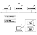
はじめに、膜厚モデルまたは屈折率モデルを生成するフェーズにおける成膜システムのシステム構成について説明する。図1は、膜厚モデルまたは屈折率モデルを生成するフェーズにおける成膜システムのシステム構成の一例を示す図である。図1に示すように、成膜システム100は、成膜装置110、膜厚測定装置120、屈折率測定装置130、情報処理装置140を有する。
(1) System Configuration of Film Forming System in Phase of Generating Film Thickness Model or Refractive Index Model First, the system configuration of the film forming system in the phase of generating a film thickness model or a refractive index model will be described. FIG. 1 is a diagram showing an example of a system configuration of a film forming system in a phase of generating a film thickness model or a refractive index model. As shown in FIG. 1 , the
成膜装置110は、複数のプラズマ源を有する枚葉の成膜装置である。成膜装置110は、所定のプロセス条件のもとで、ウェハの成膜処理を行う。また、成膜装置110は、成膜処理を行った際に用いたプロセス条件を、情報処理装置140に通知する。
The
膜厚測定装置120は、成膜処理前のウェハの各位置の膜厚と、成膜処理後のウェハの各位置の膜厚とをそれぞれ測定する。また、膜厚測定装置120は、成膜処理前及び成膜処理後にそれぞれ測定した各位置の膜厚を、情報処理装置140に通知する。
The film
屈折率測定装置130は、成膜処理前のウェハの各位置の屈折率(膜内の窒素成分の割合に関する値)と、成膜処理後のウェハの各位置の屈折率とをそれぞれ測定する。また、屈折率測定装置130は、成膜処理前及び成膜処理後にそれぞれ測定した各位置の屈折率を、情報処理装置140に通知する。
The refractive
情報処理装置140には、モデル生成プログラムがインストールされており、当該モデル生成プログラムが実行されることで、情報処理装置140は、モデル生成部150として機能する。
A model generation program is installed in the
モデル生成部150は、膜厚測定装置120より通知された、成膜処理前の膜厚及び屈折率と、成膜処理後の膜厚及び屈折率と、成膜装置110より通知された、成膜処理を行った際に用いたプロセス条件とを取得する。
The
また、モデル生成部150は、複数のプラズマ源それぞれの出力を所定量変更したプロセス条件のもとで成膜処理を行った場合の、ウェハの各位置での膜厚の変化量を規定した膜厚モデルを生成する。
In addition, the
また、モデル生成部150は、複数のプラズマ源それぞれの出力を所定量変更したプロセス条件のもとで成膜処理を行った場合の、ウェハの各位置での屈折率の変化量を規定した屈折率モデルを生成する。
The
更に、モデル生成部150は、生成した膜厚モデル及び屈折率モデルを、格納部の一例であるモデル格納部160に格納する。
Furthermore, the
(2)各プラズマ源の出力を最適化し、新レシピを生成するフェーズにおける成膜システムのシステム構成
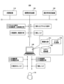
次に、生成した膜厚モデルまたは屈折率モデルを用いて各プラズマ源の出力を最適化し、新レシピを生成するフェーズにおける成膜システムのシステム構成について説明する。図2は、各プラズマ源の出力を最適化し、新レシピを生成するフェーズにおける成膜システムのシステム構成の一例を示す図である。ここでは、図1との相違点を中心に説明する。
(2) System configuration of the deposition system in the phase of optimizing the output of each plasma source and generating a new recipe Next, using the generated film thickness model or refractive index model, optimize the output of each plasma source and The system configuration of the film formation system in the recipe generation phase will be described. FIG. 2 is a diagram showing an example of the system configuration of the film formation system in the phase of optimizing the output of each plasma source and generating a new recipe. Here, the description will focus on the differences from FIG.
成膜装置110は、はじめに、現状のレシピに含まれる所定のプロセス条件のもとで、ウェハに対する成膜処理を行い、成膜処理を行った際に用いたプロセス条件を、情報処理装置140に通知する。続いて、成膜装置110は、新たなプロセス条件が通知された場合に、該新たなプロセス条件のもとで、ウェハに対する成膜処理を行う。
The
膜厚測定装置120は、現状のレシピに含まれる所定のプロセス条件のもとでウェハに対する成膜処理が行われた後の、ウェハの各位置の膜厚を測定し、初期膜厚として、情報処理装置140に通知する。また、膜厚測定装置120は、新たなプロセス条件のもとでウェハに対する成膜処理が行われた後の、ウェハの各位置の膜厚を測定し、現膜厚として、情報処理装置140に通知する。
The film thickness measuring
屈折率測定装置130は、現状のレシピに含まれる所定のプロセス条件のもとでウェハに対する成膜処理が行われた後の、ウェハの各位置の屈折率を測定し、初期屈折率として、情報処理装置140に通知する。また、屈折率測定装置130は、新たなプロセス条件のもとでウェハに対する成膜処理が行われた後の、ウェハの各位置の屈折率を測定し、現屈折率として、情報処理装置140に通知する。
Refractive
情報処理装置140には、最適化プログラムとレシピ生成プログラムとがインストールされており、当該最適化プログラム及びレシピ生成プログラムが実行されることで、情報処理装置140は、最適化部151、レシピ生成部152として機能する。
An optimization program and a recipe generation program are installed in the
最適化部151は算出部の一例であり、作業者170より、新レシピ生成用の膜厚の目標値(目標膜厚)を受け付け、初期膜厚との残差(膜厚残差)を算出する。また、最適化部151は、算出した膜厚残差と、モデル格納部160に格納された膜厚モデルとを用いて、複数のプラズマ源それぞれの出力の変更量(補正値)を算出する。
The
また、最適化部151は、新たなプロセス条件(算出した複数のプラズマ源それぞれの出力の補正値が適用されたプロセス条件)を、成膜装置110に通知する。また、最適化部151は、新たなプロセス条件のもとでウェハに対する成膜処理が行われた後の現膜厚と、目標膜厚との膜厚残差を算出する。最適化部151では、膜厚残差(の真値)がなるべく小さくなるように補正値を算出し、膜厚残差(の真値)が充分小さくなったと判定すると、複数のプラズマ源それぞれの出力の補正値を、レシピ生成部152に通知する。
In addition, the
更に、最適化部151は、当該新たなプロセス条件のもとで成膜処理が行われた場合のウェハの各位置の計算上の膜厚を、予測膜厚として算出する。
Furthermore, the
同様に、最適化部151は、作業者170より、新レシピ生成用の屈折率の目標値(目標屈折率)を受け付け、初期屈折率との残差(屈折率残差)を算出する。また、最適化部151は、算出した屈折率残差と、モデル格納部160に格納された屈折率モデルとを用いて、複数のプラズマ源それぞれの出力の変更量(補正値)を算出する。
Similarly, the
また、最適化部151は、新たなプロセス条件(算出した複数のプラズマ源それぞれの出力の補正値が適用されたプロセス条件)を、成膜装置110に通知する。また、最適化部151は、新たなプロセス条件のもとで成膜処理が行われた後の現屈折率と、目標屈折率との屈折率残差を算出する。最適化部151では、屈折率残差(の真値)がなるべく小さくなるように補正値を算出し、屈折率残差(の真値)が充分小さくなったと判定すると、複数のプラズマ源それぞれの出力の補正値をレシピ生成部152に通知する。
In addition, the
更に、最適化部151は、当該新たなプロセス条件のもとで成膜処理が行われた場合のウェハの各位置の計算上の屈折率を、予測屈折率として算出する。
Furthermore, the
レシピ生成部152は生成部の一例であり、作業者170より現状のレシピを受け付ける。また、レシピ生成部152は、最適化部151より、複数のプロセス源それぞれの出力の補正値が通知された場合に、現状のレシピを修正し、新レシピを生成する。レシピ生成部152は、生成した新レシピを、作業者170に表示するとともに、成膜装置110に通知する。
The
<成膜装置の内部構成>
次に、複数のプラズマ源を有する成膜装置110の内部構成について説明する。図3は、複数のプラズマ源を有する成膜装置の内部構成の一例を示す図である。
<Internal configuration of deposition apparatus>
Next, the internal configuration of the
図3に示すように、成膜装置110は、気密に構成されたアルミニウムまたはステンレス鋼等の金属材料からなる略円筒状をなす接地されたチャンバ300と、チャンバ300内にマイクロ波プラズマを形成するためのマイクロ波プラズマ源310とを有する。
As shown in FIG. 3, the
チャンバ300の上部には開口部300aが形成されており、この開口部300aには円板状をなす蓋体301を介してチャンバ300の内部に臨むようにマイクロ波プラズマ源310が設けられている。蓋体301は、アルミニウム等の金属製であり、チャンバ300の上部に設けられた支持リング311により支持されており、支持リング311と蓋体301との間はシールリング(図示せず)により気密にシールされている。
An
チャンバ300内にはウェハWを水平に支持するためのサセプタ302が、チャンバ300の底部中央に絶縁部材303aを介して立設された筒状の支持部材303により支持された状態で設けられている。サセプタ302および支持部材303を構成する材料としては、例えば、表面をアルマイト処理(陽極酸化処理)したアルミニウム等が挙げられる。
A
また、図示していないが、サセプタ302には、ウェハWを静電吸着するための静電チャック、温度制御機構、ウェハWの裏面に熱伝達用のガスを供給するガス流路、およびウェハWを搬送するために昇降する昇降ピン等が設けられている。更に、サセプタ302には、整合器320を介して高周波バイアス電源321が電気的に接続されている。この高周波バイアス電源321からサセプタ302に高周波電力が供給されることにより、ウェハW側にプラズマ中のイオンが引き込まれる。
Although not shown, the
チャンバ300の底部には排気管304が接続され、この排気管304には真空ポンプを含む排気装置330が接続される。そしてこの排気装置330を作動させることによりチャンバ300内が排気され、チャンバ300内を所定の真空度まで高速に減圧することができる。また、チャンバ300の側壁には、ウェハWの搬入出を行うための搬入出口305と、この搬入出口305を開閉するゲートバルブ306とが設けられている。
An
チャンバ300内のサセプタ302の上方位置には、処理ガスをウェハWに向けて吐出するシャワープレート307が水平に設けられている。このシャワープレート307は、格子状に形成されたガス流路308と、このガス流路308に形成された多数のガス吐出孔308aとを有しており、格子状のガス流路308の間は空間部308bが形成されている。このシャワープレート307のガス流路308にはチャンバ300の外側に延びる配管309が接続されている。また、この配管309には処理ガス供給源340が接続されており、シャワープレート307、配管309、および処理ガス供給源340は処理ガス用のガス供給機構を構成している。
Above the
一方、チャンバ300のシャワープレート307の上方位置には、リング状のプラズマガス導入部材350がチャンバ壁に沿って設けられており、このプラズマガス導入部材350には内周に多数のガス吐出孔が設けられている。このプラズマガス導入部材350には、プラズマガスを供給するプラズマガス供給源351が配管352を介して接続されており、プラズマガス導入部材350、配管352、およびプラズマガス供給源351はプラズマガス用のガス供給機構を構成している。プラズマガスとしてはArガスなどが好適に用いられる。
On the other hand, above the
プラズマガス導入部材350からチャンバ300内に導入されたプラズマガスは、マイクロ波プラズマ源310からチャンバ300内に導入されたマイクロ波によりプラズマ化される。プラズマ化されたプラズマガスはシャワープレート307の空間部308bを通過しシャワープレート307のガス吐出孔308aから吐出された処理ガスを励起し、処理ガスのプラズマを形成する。なお、プラズマガスと処理ガスとを同一の供給部材で供給してもよい。また、処理ガスにプラズマガスの機能をもたせてもよい。
The plasma gas introduced into the
マイクロ波プラズマ源310は、複数経路に分配してマイクロ波を出力するマイクロ波出力部312と、マイクロ波出力部312から出力されたマイクロ波を伝送しチャンバ300内に放射するためのマイクロ波供給部360とを有している。
The
マイクロ波供給部360は、マイクロ波を主に増幅する複数のアンプ部361と、各アンプ部361で増幅されたマイクロ波をそれぞれチャンバ300内へ導く複数のマイクロ波放射機構362とを有している。
The
蓋体301のマイクロ波放射機構362に対応する部分には孔301aが形成されており、孔301aには、マイクロ波放射機構362の一部をなす、マイクロ波を透過させるマイクロ波透過窓として機能する誘電体部材301bが嵌め込まれている。したがって、蓋体301および誘電体部材301bによりチャンバ300の天壁370が形成される。また、天壁370の下面には、マイクロ波放射機構362の配置領域を包含し天壁370を覆うように薄い誘電体板301cが設けられている。誘電体板301cは誘電体部材301bおよび蓋体301の両方を覆う一枚板として構成される。
A
第1の実施形態において、マイクロ波供給部360は、アンプ部361およびマイクロ波放射機構362(プラズマ源)を7個有している(図3(b)のマイクロ波放射機構362a~362g参照)。なお、図3(b)は、マイクロ波放射機構362a~362gの配置を上面から見た様子を示す図である。
In the first embodiment, the
図3(b)に示すように、マイクロ波放射機構362a~362gは、サセプタ302に水平に支持されたウェハWに対して、円周状に6個および中心に1個配置される。
As shown in FIG. 3(b), the
なお、図3(b)に示すように、本実施形態の以下の説明では、マイクロ波放射機構362aを"プラズマ源#1"、マイクロ波放射機構362bを"プラズマ源#2"、マイクロ波放射機構362cを"プラズマ源#3"と称する。また、マイクロ波放射機構362dを"プラズマ源#4"、マイクロ波放射機構362eを"プラズマ源#5"、マイクロ波放射機構362fを"プラズマ源#6"、マイクロ波放射機構362gを"プラズマ源#7"と称する。
As shown in FIG. 3B, in the following description of this embodiment, the
図3(a)の説明に戻る。図3(a)に示す成膜装置110の各構成部は、マイクロプロセッサを有する制御部380により制御される。制御部380は、成膜装置110に設定されるレシピを記憶した記憶部や、操作部、表示部等を備えており、設定されたレシピに従って成膜装置110の各構成部を制御する。
Returning to the description of FIG. Each component of the
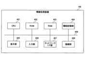
<情報処理装置のハードウェア構成>
次に、情報処理装置140のハードウェア構成について説明する。図4は、情報処理装置のハードウェア構成の一例を示す図である。図4に示すように、情報処理装置140は、CPU(Central Processing Unit)401、ROM(Read Only Memory)402、RAM(Random Access Memory)403を有する。CPU401、ROM402、RAM403は、いわゆるコンピュータを形成する。
<Hardware Configuration of Information Processing Device>
Next, the hardware configuration of the
また、情報処理装置140は、補助記憶部404、表示部405、入力部406、ネットワークI/F(Interface)部407、接続部408を有する。なお、情報処理装置140の各ハードウェアは、バス409を介して相互に接続されている。
The
CPU401は、補助記憶部404にインストールされている各種プログラム(例えば、モデル生成プログラム、最適化プログラム、レシピ生成プログラム等の情報処理プログラム)を実行するデバイスである。
The
ROM402は、不揮発性メモリである。ROM402は、補助記憶部404にインストールされている各種プログラムをCPU401が実行するために必要な各種プログラムやデータ等を格納する、主記憶デバイスとして機能する。具体的には、ROM402はBIOS(Basic Input/Output System)やEFI(Extensible Firmware Interface)等のブートプログラム等を格納する。
RAM403は、DRAM(Dynamic Random Access Memory)やSRAM(Static Random Access Memory)等の揮発性メモリである。RAM403は、補助記憶部404にインストールされている各種プログラムがCPU401によって実行される際に展開される作業領域を提供する、主記憶デバイスとして機能する。
A
補助記憶部404は、各種プログラムや、各種プログラムが実行される際に用いられる情報を格納する補助記憶デバイスである。モデル格納部160は、補助記憶部404において実現される。
The
表示部405は、各種プログラムが実行されることで生成される画面(例えば、予測膜厚、予測屈折率、新レシピを含む画面等)を表示する、表示デバイスである。入力部406は、情報処理装置140に対して、作業者170等が各種指示(例えば、目標膜厚、目標屈折率、現状のレシピ等)を入力するための入力デバイスである。
The
ネットワークI/F部407は、不図示の外部ネットワークと接続する通信デバイスである。接続部408は、成膜装置110、膜厚測定装置120、屈折率測定装置130等の各種装置と接続するための接続デバイスである。
A network I/
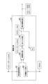
<モデル生成部の機能構成>
次に、情報処理装置140のモデル生成部150の詳細について説明する。図5は、モデル生成部の機能構成の一例を示す図である。
<Functional configuration of the model generator>
Next, details of the
図5に示すように、モデル生成部150は、モデル生成用データ取得部501と、生成部502とを有する。
As shown in FIG. 5 , the
モデル生成用データ取得部501は、膜厚モデル及び屈折率モデルの生成用に、成膜装置110がウェハ(モデル生成処理時の処理対象である第1のウェハ)に対して成膜処理を行った際の、各種データを取得する。第1の実施形態において、膜厚モデル及び屈折率モデル生成用の成膜処理とは、第1の処理手順で行われる成膜処理を指す。なお、第1の処理手順とは、例えば、複数のプラズマ源#1~#7の出力以外のプロセス条件を固定した状態で、複数のプラズマ源#1~#7それぞれの出力を所定量変更する処理手順を指す。
In the model generation
ただし、膜厚モデル及び屈折率モデル生成用の成膜処理は、第1の処理手順で行われる成膜処理に限定されない。例えば、実験計画法(直交表)を用いて、複数のプラズマ源♯1~♯7の出力を同時に変更する第2の処理手順で行われる成膜処理であってもよい。あるいは、他の方法(例えば、PLS(Partial Least Squares)やDL(Deep Learning))により、膜厚モデル及び屈折率モデルを生成する場合にあっては、他の方法に適した他の処理手順で成膜処理を行ってもよい。なお、以下では、説明の簡略化のため、膜厚モデル及び屈折率モデル生成用の成膜処理が、第1の処理手順で行われるものとして説明する。
However, the film formation process for generating the film thickness model and the refractive index model is not limited to the film formation process performed in the first procedure. For example, the film formation process may be performed in the second process procedure in which the outputs of the plurality of
モデル生成用データ取得部501は、成膜装置110より、複数のプラズマ源#1~#7の出力(所定量変更後の出力)を、複数のプラズマ源#1~#7の出力以外のプロセス条件とともに取得する。
The model generation
また、モデル生成用データ取得部501は、膜厚モデル生成用の成膜処理が行われた際の、成膜処理前のウェハの各位置の膜厚と成膜処理後のウェハの各位置の膜厚とを、膜厚測定装置120より取得する。
In addition, the model generation
また、モデル生成用データ取得部501は、屈折率モデル生成用の成膜処理が行われた際の、成膜処理前のウェハの各位置の屈折率と成膜処理後のウェハの各位置の屈折率とを、屈折率測定装置130より取得する。
The model generation
生成部502は、膜厚モデル生成用の成膜処理が行われた際の、ウェハの各位置での膜厚の変化量から、単位量(例えば、1[W])あたりの膜厚の変化量を算出することで、膜厚モデルを生成する。
The
また、生成部502は、屈折率モデル生成用の成膜処理が行われた際の、ウェハの各位置での屈折率の変化量から、単位量(例えば、1[W])あたりの屈折率の変化量を算出することで、屈折率モデルを生成する。
In addition, the
更に、生成部502は、生成した膜厚モデル及び屈折率モデルを、モデル格納部160に格納する。
Furthermore, the
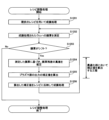
<モデル生成処理の流れ>
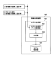
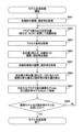
次に、成膜システム100において、膜厚モデル及び屈折率モデル生成用の成膜処理が行われることで実行されるモデル生成処理の流れについて説明する。図6は、膜厚モデル及び屈折率モデルを生成するモデル生成処理の流れを示すフローチャートの一例である。
<Flow of model generation processing>
Next, a flow of model generation processing executed by performing film formation processing for generating a film thickness model and a refractive index model in the
ステップS601において、情報処理装置140のモデル生成用データ取得部501は、膜厚測定装置120及び屈折率測定装置130より、膜厚モデル及び屈折率モデル生成用の成膜処理を行う前の、ウェハの各位置の膜厚及び屈折率を取得する。なお、モデル生成用データ取得部501が膜厚及び屈折率を取得するウェハの各位置の数は、例えば、49箇所であるとする。
In step S<b>601 , the model generation
ステップS602において、成膜装置110は、複数のプラズマ源#1~#7のうちの1のプラズマ源(例えば、プラズマ源#1)の出力を、デフォルトの値から所定量(例えば、50[W])変更して、成膜処理を行う。
In step S602, the
ステップS603において、情報処理装置140のモデル生成用データ取得部501は、成膜装置110より、ステップS602において成膜処理を行った際に用いたプロセス条件を取得する。
In step S<b>603 , the model generation
ステップS604において、膜厚測定装置120及び屈折率測定装置130は、成膜処理後のウェハの各位置の膜厚及び屈折率を測定する。
In step S604, the film
ステップS605において、情報処理装置140のモデル生成用データ取得部501は、膜厚測定装置120及び屈折率測定装置130より、成膜処理後のウェハの各位置の膜厚及び屈折率を取得する。
In step S605, the model generation
ステップS606において、情報処理装置140の生成部502は、ウェハの各位置の単位量(例えば、1[W])あたりの膜厚の変化量及び屈折率の変化量を算出する。
In step S606, the
ステップS607において、情報処理装置140の生成部502は、算出した膜厚の変化量を膜厚モデルMTの1つとしてモデル格納部160に格納する。また、情報処理装置140の生成部502は、算出した屈折率の変化量を屈折率モデルMRの1つとしてモデル格納部160に格納する。
In step S607, the
ステップS608において、情報処理装置140の生成部502は、膜厚モデル及び屈折率モデルの生成が完了したか否かを判定する。ステップS608において、膜厚モデル及び屈折率モデルの生成が完了していないと判定した場合には(ステップS608においてNoの場合には)、ステップS602に戻る。一方、ステップS608において、膜厚モデル及び屈折率モデルの生成が完了したと判定した場合には、モデル生成処理を終了する。
In step S608, the
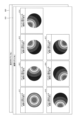
<モデル生成処理の具体例>
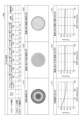
次に、成膜システム100によるモデル生成処理の具体例について図7及び図8を用いて説明する。図7は、モデル生成処理の具体例を示す第1の図であり、情報処理装置140のモデル生成用データ取得部501が成膜装置110より取得する、膜厚モデル生成用の成膜処理を行った際に用いたプロセス条件の具体例を示す図である。
<Specific example of model generation processing>
Next, a specific example of model generation processing by the
図7に示すように、プロセス条件700には、情報の項目として、"プロセスデータの種類"、"プロセスデータ"が含まれる。"プロセスデータの種類"には、チャンバ300内の圧力、プラズマガス供給源351より供給されるプラズマガスの流量、各プラズマ源#1~#7の出力、チャンバ300内の温度、成膜時間等が含まれる。また、"プロセスデータ"には、"プロセスデータの種類"に対応する値が格納される。なお、説明の簡略化のため、プロセス条件700では、プラズマ源#1~#7の出力以外のプロセス条件については、一部のみを抜粋して記載している。
As shown in FIG. 7, the
上述したように、膜厚モデル及び屈折率モデル生成用の成膜処理では、プロセス条件700のうち、プロセスデータの種類="プラズマ源#1の出力"~"プラズマ源#7の出力"それぞれのプロセスデータを、所定量(例えば、50[W])変更する。
As described above, in the film formation process for generating the film thickness model and the refractive index model, among the
図8は、モデル生成処理の具体例を示す第2の図であり、膜厚モデル(MT)810及び屈折率モデル(MR)820の具体例を示す図である。膜厚モデル(MT)810の符号811は、プラズマ源#1の出力を、所定量変更して成膜処理を行った場合の、ウェハの各位置の膜厚の変化量から、単位量あたりの変化量を算出した算出結果(膜厚分布の変化)を、カラーマップとして可視化したものである。
FIG. 8 is a second diagram showing a specific example of model generation processing, and is a diagram showing specific examples of a film thickness model (M T ) 810 and a refractive index model (M R ) 820. In FIG.
同様に、符号812は、プラズマ源#2の出力を、所定量変更して成膜処理を行った場合の、ウェハの各位置の膜厚の変化量から、単位量あたりの変化量を算出した算出結果(膜厚分布の変化)を、カラーマップとして可視化したものである。
Similarly,
同様に、符号813は、プラズマ源#3の出力を、所定量変更して成膜処理を行った場合の、ウェハの各位置の膜厚の変化量から、単位量あたりの変化量を算出した算出結果(膜厚分布の変化)を、カラーマップとして可視化したものである。
Similarly,
同様に、符号814は、プラズマ源#4の出力を、所定量変更して成膜処理を行った場合の、ウェハの各位置の膜厚の変化量から、単位量あたりの変化量を算出した算出結果(膜厚分布の変化)を、カラーマップとして可視化したものである。
Similarly,
同様に、符号815は、プラズマ源#5の出力を、所定量変更して成膜処理を行った場合の、ウェハの各位置の膜厚の変化量から、単位量あたりの変化量を算出した算出結果(膜厚分布の変化)を、カラーマップとして可視化したものである。
Similarly,
同様に、符号816は、プラズマ源#6の出力を、所定量変更して成膜処理を行った場合の、ウェハの各位置の膜厚の変化量から、単位量あたりの変化量を算出した算出結果(膜厚分布の変化)を、カラーマップとして可視化したものである。
Similarly,
同様に、符号817は、プラズマ源#7の出力を、所定量変更して成膜処理を行った場合の、ウェハの各位置の膜厚の変化量から、単位量あたりの変化量を算出した算出結果(膜厚分布の変化)を、カラーマップとして可視化したものである。
Similarly,
このように、モデル生成部150では、膜厚モデル生成用の成膜処理が行われることで、プラズマ源#1~#7の数に応じた数の算出結果(符号811~817)を含む膜厚モデル(MT)810を生成する。同様に、モデル生成部150では、屈折率モデル生成用の成膜処理が行われることで、プラズマ源#1~#7の数に応じた数の算出結果を含む屈折率モデル(MR)820を生成する。なお、膜厚モデル及び屈折率モデル生成用の成膜処理が第2の処理手順によって行われる場合にあっては、プラズマ源#1~#7は複数のゾーンに分類される。このため、ゾーンの数に応じた数の算出結果を含む膜厚モデル(MT)及び屈折率モデル(MR)が生成されることになる。
In this way, in the
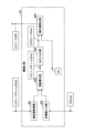
<最適化部及びレシピ生成部の機能構成>
次に、情報処理装置140の最適化部151及びレシピ生成部152の機能構成について説明する。図9は、最適化部及びレシピ生成部の機能構成の一例を示す図である。
<Functional configuration of optimization unit and recipe generation unit>
Next, functional configurations of the
図9に示すように、最適化部151は、測定値取得部901、目標値入力部902、残差算出部903、カルマンフィルタ部904、補正値算出部905を有する。
As shown in FIG. 9 , the
測定値取得部901は、成膜装置110より、現状のレシピにより成膜処理が行われた際に用いられたプロセス条件を取得する。また、測定値取得部901は、膜厚測定装置120及び屈折率測定装置130より、現状のレシピにより成膜処理が行われた後の、ウェハ(新レシピ生成処理時の処理対象である第2のウェハ)の各位置の膜厚及び屈折率を、初期膜厚及び初期屈折率として取得する。
A measurement
また、測定値取得部901は、新たなプロセス条件(複数のプラズマ源の出力の補正値が適用されたプロセス条件)のもとで成膜装置110により成膜処理が行われた後の、ウェハの各位置の膜厚及び屈折率を、現膜厚及び現屈折率として取得する。
In addition, the measurement
目標値入力部902は、作業者170より、目標膜厚及び目標屈折率の入力を受け付ける。
A target
残差算出部903は、初期膜厚と目標膜厚との差分または現膜厚と目標膜厚との差分である膜厚残差を算出する。また、残差算出部903は、初期屈折率と目標屈折率との差分または現屈折率と目標屈折率との差分である屈折率残差を算出する。
The
カルマンフィルタ部904は、カルマンゲインを調整することで、残差算出部903により算出された膜厚残差及び屈折率残差の真値を推定する。なお、膜厚測定装置120及び屈折率測定装置130がウェハの各位置の膜厚及び屈折率を測定した際の測定結果には測定誤差が含まれているものとする。
The
補正値算出部905は、カルマンフィルタ部904により推定された膜厚残差の真値及び屈折率残差の真値と、モデル格納部160に格納された膜厚モデル(MT)810及び屈折率モデル(MR)820とを取得する。また、補正値算出部905は、取得した膜厚残差の真値及び屈折率残差の真値と、膜厚モデル(MT)810及び屈折率モデル(MR)820とに基づいて、複数のプラズマ源#1~#7の出力の補正値を算出する。また、補正値算出部905は、算出した複数のプラズマ源#1~#7の出力の補正値を適用した新たなプロセス条件を、成膜装置110に通知する。
The correction
また、補正値算出部905は、膜厚残差の真値及び屈折率残差の真値がなるべく小さくなるように補正値を算出する。そして、補正値算出部905では、真値が充分小さくなった判定すると、複数のプラズマ源#1~#7の出力の補正値(複数回算出された場合には複数回分の補正値の合計値)を、新レシピ生成部906に通知する。
Further, the correction
また、補正値算出部905は、
・初期膜厚と、
・膜厚モデル(MT)810と、
・複数のプラズマ源#1~#7の出力の補正値(複数回算出された場合には複数回分の補正値の合計値)と、
に基づいて、当該新たなプロセス条件のもとで成膜処理が行われた場合のウェハの各位置の計算上の膜厚を、予測膜厚として算出し、作業者170に表示する。
Further, the correction
・Initial film thickness and
a film thickness model (M T ) 810;
A correction value for the output of a plurality of
, the calculated film thickness at each position of the wafer when film formation is performed under the new process conditions is calculated as a predicted film thickness and displayed to the
また、補正値算出部905は、
・初期屈折率と、
・屈折率モデル(MR)820と、
・複数のプラズマ源#1~#7の出力の補正値(複数回算出された場合には複数回分の補正値の合計値)と、
に基づいて、当該新たなプロセス条件のもとで成膜処理が行われた場合のウェハの各位置の計算上の屈折率を、予測屈折率として算出し、作業者170に表示する。
Further, the correction
an initial refractive index;
a refractive index model (M R ) 820;
A correction value for the output of a plurality of
, the calculated refractive index at each position of the wafer when film formation is performed under the new process conditions is calculated as a predicted refractive index and displayed to the
レシピ生成部152は、新レシピ生成部906を有する。新レシピ生成部906は、作業者170より、現状のレシピの入力を受け付ける。また、新レシピ生成部906は、補正値算出部905より通知された、複数のプラズマ源#1~#7の出力の補正値(複数回算出された場合には複数回分の補正値の合計値)を用いて、現状のレシピを修正し、新レシピを生成する。更に、新レシピ生成部906は、生成した新レシピを作業者170に表示するとともに、成膜装置110に通知する。
The
<最適化部における処理の詳細>
次に、最適化部151における処理の詳細(主に、カルマンフィルタ部904の処理の詳細)について数式を用いて説明する。なお、ここでは、説明の簡略化のために、新レシピ生成用の目標値として、目標膜厚の入力を受け付ける場合について説明する(目標屈折率の入力を受け付ける場合については、目標膜厚の入力を受け付ける場合と同様であるため、説明を省略する)。
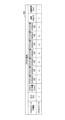
<Details of processing in the optimization unit>
Next, the details of the processing in the optimization unit 151 (mainly the details of the processing in the Kalman filter unit 904) will be described using mathematical expressions. In order to simplify the explanation, the case where the input of the target film thickness is accepted as the target value for generating a new recipe will be explained here (in the case of accepting the input of the target refractive index, the input of the target film thickness is Since it is the same as the case of receiving, the explanation is omitted).
図10は、最適化部における処理の詳細を説明するための図である。このうち、図10(a)は、
・最適化部151の補正値算出部905で算出されるプラズマ源の出力の補正値と、
・最適化部151の残差算出部903で算出される膜厚残差と、
の間の入出力関係を模式的に示した図である。
FIG. 10 is a diagram for explaining details of processing in the optimization unit. Among them, FIG.
A correction value for the output of the plasma source calculated by the correction
The film thickness residual calculated by the
1 is a diagram schematically showing an input/output relationship between;
なお、図10(a)に示す各記号の意味は、下記のとおりである。
・k:時間ステップ(プラズマ源の出力の補正値が成膜装置110に通知された回数)
・u(k):プラズマ源の出力の補正値、
・w(k):システムノイズ、
・x(k+1):k回目の補正値が通知されることで変化する、変化後の成膜装置110の状態、
・x(k):k回目の補正値が通知される前の、成膜装置110の状態、
・y(k):k回目の補正値が通知される前の、膜厚残差(現膜厚-目標膜厚)の真値、
・vT:膜厚に関する測定誤差、
・z(k):k回目の補正値が通知される前の、現膜厚に基づいて算出される膜厚残差。
The meaning of each symbol shown in FIG. 10(a) is as follows.
・k: time step (the number of times the plasma source output correction value is notified to the film forming apparatus 110)
u(k): correction value for plasma source output;
w(k): system noise;
x(k+1): the state of the
x(k): the state of the
· y (k): the true value of the film thickness residual (current film thickness - target film thickness) before the k-th correction value is notified,
・v T : measurement error related to film thickness,
z(k): film thickness residual calculated based on the current film thickness before the k-th correction value is notified.
最適化部151のカルマンフィルタ部904では、
・最適化部151の補正値算出部905で算出されるプラズマ源の出力の補正値と、
・最適化部151の残差算出部903で算出される膜厚残差と、
の間の入出力関係(図10(a))に基づいて、カルマンフィルタを構成し、カルマンゲインを調整する(図10(b)参照)。
In the
A correction value for the output of the plasma source calculated by the correction
The film thickness residual calculated by the
A Kalman filter is configured based on the input/output relationship (FIG. 10(a)) between and the Kalman gain is adjusted (see FIG. 10(b)).
なお、図10(b)は、図10(a)に示す入出力関係に基づいて、カルマンフィルタ部904において構成されたカルマンフィルタの一例である。
FIG. 10(b) is an example of a Kalman filter configured in the
最適化部151のカルマンフィルタ部904では、補正値算出部905がプラズマ源の出力の補正値を通知するごとに、残差算出部903より膜厚残差を取得し、カルマンゲインを調整することで、膜厚残差の真値を推定する。
In the
なお、図10(b)に示す各記号において、例えば、 For each symbol shown in FIG. 10(b), for example,

同様に、例えば、 Similarly, for example,

<新レシピ生成処理の流れ>
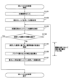
次に、新レシピ生成処理の流れについて説明する。図11Aは、新レシピ生成処理の流れを示すフローチャートである。
<New recipe generation process flow>
Next, the flow of new recipe generation processing will be described. FIG. 11A is a flowchart showing the flow of new recipe generation processing.
ステップS1101において、目標値入力部902は、作業者170より、目標膜厚の入力を受け付ける。
In step S<b>1101 , the target
ステップS1102において、成膜装置110は、現状のレシピを用いて成膜処理を行う。
In step S1102, the
ステップS1103において、膜厚測定装置120は、ステップS1102において成膜処理が行われたウェハの各位置の膜厚を測定する。
In step S1103, the film
ステップS1104において、測定値取得部901は、ステップS1103において測定されたウェハの各位置の膜厚を初期膜厚として取得する。また、残差算出部903は、取得された初期膜厚が、目標膜厚と一致するか否かを判定する。
In step S1104, the measurement
ステップS1104において、一致すると判定した場合には(ステップS1104においてYesの場合には)、新レシピ生成処理を終了する。一方、ステップS1104において、一致しないと判定した場合には(ステップS1104においてNoの場合には)、ステップS1105に進む。以降、ステップS1105~S1106において、最適化部151では、各プラズマ源#1~#7の出力の補正値を算出する工程を実行する。
If it is determined in step S1104 that they match (in the case of Yes in step S1104), the new recipe generation processing ends. On the other hand, if it is determined in step S1104 that they do not match (No in step S1104), the process proceeds to step S1105. After that, in steps S1105 and S1106, the
ステップS1105において、残差算出部903は、初期膜厚と目標膜厚との差分に基づいて膜厚残差を算出する。また、カルマンフィルタ部904は、カルマンゲインを調整することで、膜厚残差の真値を推定する。
In step S1105, the
ステップS1106において、補正値算出部905は、膜厚残差の真値と膜厚モデル(MT)とに基づいて、各プラズマ源#1~#7の出力の補正値を算出する。また、補正値算出部905は、算出した各プラズマ源#1~#7の出力の補正値(複数回算出した場合には複数回分の補正値の合計値)を適用した新たなプロセス条件を、成膜装置110に通知する。
In step S1106, the
ステップS1107において、成膜装置110は、通知された新たなプロセス条件のもとで成膜処理を行い、ステップS1103に戻る。以降、ステップS1103において測定される現膜厚が、ステップS1104において、目標膜厚と一致すると判定されるまで、ステップS1103~S1107の処理を繰り返す。そして、ステップS1104において、目標膜厚と一致すると判定された場合には(ステップS1104においてYesの場合には)、新レシピ生成処理を終了する。
In step S1107, the
なお、図11Aでは、新レシピ生成処理の流れについて示したが、レシピ調整処理の流れも同様である。 Although FIG. 11A shows the flow of the new recipe generation process, the flow of the recipe adjustment process is the same.
図11Bは、レシピ調整処理の流れを示すフローチャートであり、Run to Run時の処理の流れを示している。なお、図11Bに示す処理内容は、図11Aに示した処理内容と概ね同じであるため、ここでは、詳細な説明を省略する。 FIG. 11B is a flowchart showing the flow of recipe adjustment processing, and shows the flow of processing during Run to Run. Note that the processing content shown in FIG. 11B is substantially the same as the processing content shown in FIG. 11A, so detailed description thereof will be omitted here.
<新レシピ生成処理の具体例>
次に、新レシピ生成処理において最適化部151が行う処理の具体例について説明する。図12は、新レシピ生成処理において最適化部が行う処理の具体例を示す第1の図である。
<Specific example of new recipe generation processing>
Next, a specific example of processing performed by the
図12の例は、現状のレシピに基づいて成膜処理が行われることで、測定値取得部901が、膜厚測定装置120から、初期膜厚として、v(1)=(40+vT)[nm]を取得した様子を示している。
In the example of FIG. 12, the film formation process is performed based on the current recipe, and the measurement
また、図12の例は、目標値入力部902が、目標膜厚として、作業者170により、目標膜厚=50[nm]が入力された様子を示している。
Also, the example of FIG. 12 shows a state in which the
また、図12の例は、残差算出部903が、初期膜厚と目標膜厚との差分を算出することで、膜厚残差として、z(1)=(-10+vT)[nm]を算出した様子を示している。
In the example of FIG. 12, the
また、図12の例は、カルマンフィルタ部904が、膜厚残差に基づいて、膜厚残差の真値として、-10[nm]を推定した様子を示している。
Also, the example of FIG. 12 shows how the
また、図12の例は、補正値算出部905が、膜厚残差の真値(=-10[nm])がなるべく小さくなるように、膜厚モデル(MT)と膜厚残差とに基づいて、各プラズマ源の出力の補正値を算出し、u(1)=20[W]を出力した様子を示している。
Further, in the example of FIG. 12, the correction
図13は、新レシピ生成処理において最適化部が行う処理の具体例を示す第2の図である。図13の例は、図12において算出された、各プラズマ源の出力の補正値(u(1)=20[W])が適用された新たなプロセス条件のもとで成膜処理が行われた後の、最適化部151による処理を示している。具体的には、測定値取得部901が、膜厚測定装置120から、現膜厚として、v(2)=(70+vT)[nm]を取得した様子を示している。
FIG. 13 is a second diagram illustrating a specific example of processing performed by the optimization unit in the new recipe generation processing. In the example of FIG. 13, the film formation process is performed under new process conditions to which the correction value (u(1)=20 [W]) of the output of each plasma source calculated in FIG. 12 is applied. It shows the processing by the
また、図13の例は、残差算出部903が、現膜厚と目標膜厚との差分を算出することで、膜厚残差として、v(2)=(20+vT)[nm]を算出した様子を示している。
Further, in the example of FIG. 13, the
また、図13の例は、カルマンフィルタ部904が、膜厚残差に基づいて、膜厚残差の真値として、20[nm]を推定した様子を示している。
Also, the example of FIG. 13 shows how the
また、図13の例は、補正値算出部905が、膜厚残差の真値(=20[nm])がなるべく小さくなるように、膜厚モデル(MT)と膜厚残差とに基づいて、各プラズマ源の出力の補正値を算出し、u(2)=13[W]を出力した様子を示している。
In addition, in the example of FIG. 13, the correction
図14は、新レシピ生成処理の具体例を示す第3の図である。図14の例は、図13において算出された、各プラズマ源の出力の補正値(u(2)=13[W])を適用した新たなプロセス条件のもとで成膜処理が行われた後の、最適化部151による処理を示している。具体的には、測定値取得部901が、膜厚測定装置120から、現膜厚として、v(3)=(50+vT)[nm]を取得した様子を示している。
FIG. 14 is a third diagram showing a specific example of new recipe generation processing. In the example of FIG. 14, the film formation process was performed under new process conditions using the correction value of the output of each plasma source (u(2)=13 [W]) calculated in FIG. It shows the subsequent processing by the
また、図14の例は、残差算出部903が、現膜厚と目標膜厚との差分を算出することで、膜厚残差として、z(3)=(0+vT)[nm]を算出した様子を示している。
Further, in the example of FIG. 14, the
また、図14の例は、カルマンフィルタ部904が、膜厚残差に基づいて、膜厚残差の真値として、0[nm]を推定した様子を示している。
Also, the example of FIG. 14 shows how the
また、図14の例は、膜厚残差の真値が0[nm]になったことで、膜厚残差の真値が充分小さくなったと判定された様子を示している。 Further, the example of FIG. 14 shows a state in which it is determined that the true value of the film thickness residual has become sufficiently small since the true value of the film thickness residual has become 0 [nm].
また、図14の例は、補正値算出部905が、各プラズマ源の出力の補正値(例えば、プラズマ源#1の出力の複数回分の補正値u(1)=20[W]、u(2)=13[W])を、新レシピ生成部906に通知した様子を示している。
Further, in the example of FIG. 14, the correction
このように、成膜装置110において所望の膜厚を実現する新たなレシピを生成する際、情報処理装置140の最適化部151では、各プラズマ源の出力の補正値を自動的に算出する。これにより、作業者170は、最適化部151により算出された補正値を適用した新たなプロセス条件に従って成膜処理を行うだけで、各プラズマ源の出力を最適化することができる。つまり、情報処理装置140によれば、作業者170のノウハウに依存することなく、複数のプラズマ源の出力を最適化することができる。
As described above, when a new recipe for realizing a desired film thickness is generated in the
<新レシピによる成膜処理>
次に、新レシピによる成膜処理について説明する。図15は、新レシピによる成膜処理の結果を示す第1の図である。図15において、プロセス条件1500のうち、上段のプロセスデータは、現状のレシピに含まれるプロセスデータを示しており、下段のプロセスデータは、新レシピに含まれるプロセスデータを示している。
<Film formation processing with new recipe>
Next, a film forming process using a new recipe will be described. FIG. 15 is a first diagram showing the result of the film formation process using the new recipe. In FIG. 15, of the
また、図15において、符号1510は、現状のレシピを用いて成膜処理が行われた場合の、ウェハの各位置での膜厚の分布(つまり、初期の膜厚分布)をカラーマップとして可視化したものである。また、符号1511は、各径方向の初期膜厚の平均値を示している。
Further, in FIG. 15,
一方、符号1520は、新レシピを用いて成膜処理が行われた場合の、ウェハの各位置での予測の膜厚分布をカラーマップとして可視化したものである。また、符号1521は、各径方向の予測の膜厚の平均値を示している。
On the other hand,
また、符号1530は、新レシピを用いて成膜処理が行われた場合の、ウェハの各位置での実際の膜厚分布をカラーマップとして可視化したものである。また、符号1531は、各径方向の実際の膜厚の平均値を示している。
符号1511と符号1521及び符号1531との対比から明らかなように、符号1511の場合、径方向の膜厚の変動が大きい。一方、符号1521及び符号1531の場合、径方向の膜厚の変動が小さい。
As is clear from the comparison between reference numeral 1511 and
このように、プラズマ源ごとに生成した膜厚モデルに基づいて最適化した新レシピを用いることで、ウェハの表面状態のうち、表面形状に関わる膜厚の均一性を向上させることができる。 By using the new recipe optimized based on the film thickness model generated for each plasma source in this way, it is possible to improve the film thickness uniformity related to the surface shape among the wafer surface conditions.
また、符号1521と符号1531との対比から明らかなように、新レシピを用いて成膜処理を行った場合の、ウェハの各位置での予測膜厚の平均値と、ウェハの各位置での膜厚の実測値の平均値とは、概ね同じである。つまり、情報処理装置140によれば、予測膜厚を精度よく算出することができる。
Also, as is clear from the comparison between
<まとめ>
以上の説明から明らかなように、第1の実施形態に係る情報処理装置140では、
・複数のプラズマ源を有する成膜装置の各プラズマ源の出力を所定量変更して成膜処理を行った場合の、ウェハの各位置での膜厚または屈折率の変化量を取得する。
・各プラズマ源の出力を変更した際の変更量に対する、ウェハの各位置での膜厚または屈折率の変化量を算出することで、膜厚モデルまたは屈折率モデルを生成する。
・目標膜厚または目標屈折率を実現するための、各プラズマ源の出力の補正値を、生成した膜厚モデルまたは屈折率モデルに基づいて算出する。
<Summary>
As is clear from the above description, in the
Acquiring the amount of change in film thickness or refractive index at each position on the wafer when film formation is performed by changing the output of each plasma source of a film formation apparatus having a plurality of plasma sources by a predetermined amount.
Generating a film thickness model or a refractive index model by calculating the amount of change in film thickness or refractive index at each position on the wafer with respect to the amount of change when the output of each plasma source is changed.
• Calculate a correction value for the output of each plasma source to achieve the target film thickness or target refractive index based on the generated film thickness model or refractive index model.
これにより、作業者は、算出された補正値が適用された新たなプロセス条件に従って成膜処理を行うことで、各プラズマ源の出力を最適化することができる。 Thereby, the operator can optimize the output of each plasma source by performing the film forming process according to the new process conditions to which the calculated correction value is applied.
このように、第1の実施形態に係る情報処理装置140によれば、複数のプラズマ源の出力を最適化する作業を支援することができる。
Thus, according to the
[第2の実施形態]
上記第1の実施形態において、補正値算出部905は、膜厚モデルを用いて、膜厚残差の真値がなるべく小さくなるよう、各プラズマ源の出力の補正値を算出するものとして説明した。しかしながら、各プラズマ源の出力の補正値の算出方法はこれに限定されない。
[Second embodiment]
In the first embodiment described above, the correction
例えば、膜厚モデルと、各プラズマ源の出力の補正値と、膜厚残差の真値とを含む関数を2乗した値を目的関数とし、各プラズマ源の出力の補正値の上下限値を制約条件とした2次計画法により算出してもよい。これにより、第2の実施形態によれば、上下限値の範囲内で、膜厚残差の真値がなるべく小さくなるよう、各プラズマ源の出力の補正値を算出することができる。 For example, a value obtained by squaring a function including a film thickness model, a correction value of the output of each plasma source, and a true value of the film thickness residual is used as the objective function, and upper and lower limits of the correction value of the output of each plasma source may be calculated by a quadratic programming method with a constraint condition. Thus, according to the second embodiment, it is possible to calculate the correction value of the output of each plasma source so that the true value of the film thickness residual is as small as possible within the range of the upper and lower limits.
[第3の実施形態]
上記第1の実施形態では、各プラズマ源の出力を所定量変更することで、膜厚モデル及び屈折率モデルを生成するものとして説明した。しかしながら、膜厚モデル及び屈折率モデルの生成方法はこれに限定されず、例えば、プラズマガスの流量を所定量変更することで、膜厚モデル及び屈折率モデルを生成してもよい。これにより、プラズマガスの流量を最適化することができる。
[Third embodiment]
In the first embodiment, the film thickness model and the refractive index model are generated by changing the output of each plasma source by a predetermined amount. However, the method of generating the film thickness model and the refractive index model is not limited to this. For example, the film thickness model and the refractive index model may be generated by changing the flow rate of the plasma gas by a predetermined amount. Thereby, the flow rate of the plasma gas can be optimized.
このように、各プラズマ源の出力に加えて、プラズマガスの流量を最適化することで、各プラズマ源の出力のみを最適化する場合と比較して、屈折率の均一性をより向上させることができる。 By optimizing the plasma gas flow rate in addition to the output of each plasma source in this way, the uniformity of the refractive index can be further improved compared to the case where only the output of each plasma source is optimized. can be done.
なお、本実施形態の場合、最適化部151では、2種類の膜厚モデルとして、
・各プラズマ源の出力を所定量変更することで生成した膜厚モデル(第1の膜厚モデル)と、
・各ガス流路のプラズマガスの流量を所定量変更することで生成した膜厚モデル(第2の膜厚モデル)と、
を用いて、各プラズマ源の出力と各ガス流路のプラズマガスの流量とを最適化する。
In addition, in the case of this embodiment, the
a film thickness model (first film thickness model) generated by changing the output of each plasma source by a predetermined amount;
a film thickness model (second film thickness model) generated by changing the flow rate of the plasma gas in each gas flow path by a predetermined amount;
is used to optimize the power of each plasma source and the flow rate of plasma gas in each gas flow path.
同様に、本実施形態の場合、最適化部151では、2種類の屈折率モデルとして、
・各プラズマ源の出力を所定量変更することで生成した屈折率モデル(第1の屈折率モデル)と、
・各ガス流路のプラズマガスの流量を所定量変更することで生成した屈折率モデル(第2の屈折率モデル)と、
を用いて、各プラズマ源の出力と各ガス流路のプラズマガスの流量とを最適化する。
Similarly, in the case of this embodiment, the
- a refractive index model (first refractive index model) generated by changing the output of each plasma source by a predetermined amount;
a refractive index model (second refractive index model) generated by changing the flow rate of the plasma gas in each gas channel by a predetermined amount;
is used to optimize the power of each plasma source and the flow rate of plasma gas in each gas flow path.
あるいは、最適化部151では、
・各プラズマ源の出力を所定量変更することで生成した膜厚モデルと、
・各ガス流路のプラズマガスの流量を所定量変更することで生成した屈折率モデルと、
を用いて、各プラズマ源の出力と各ガス流路のプラズマガスの流量とを最適化してもよい。
Alternatively, in the
A film thickness model generated by changing the output of each plasma source by a predetermined amount,
- A refractive index model generated by changing the flow rate of the plasma gas in each gas flow path by a predetermined amount,
may be used to optimize the power output of each plasma source and the flow rate of plasma gas in each gas flow path.
[第4の実施形態]
上記第1の実施形態では、カルマンフィルタ部904がカルマンゲインを調整することにより、膜厚残差及び屈折率残差の真値を推定するものとして説明した。しかしながら、真値の推定方法はこれに限定されず、他の学習機能を用いて真値を推定するように構成してもよい。
[Fourth embodiment]
In the first embodiment described above, the
[第5の実施形態]
上記第1の実施形態では、プロセス条件700のうち、各プラズマ源の出力以外のプロセス条件を固定するものとして説明した。しかしながら、各プラズマ源の出力以外のプロセス条件であっても、例えば、成膜時間やALD(Atomic Layer Deposition)サイクルについては最適化の対象としてもよい。現状のレシピにより成膜処理が行われた際の成膜時間と膜厚の変化量との関係に基づいて、予め成膜レートを算出しておくことで、最適化部151では、最適化した成膜時間に応じた予測膜厚または予測屈折率を算出することができるからである。
[Fifth embodiment]
In the first embodiment described above, among the
また、上記第1の実施形態では、情報処理プログラムが、情報処理装置140の補助記憶部404に格納されるものとして説明した。しかしながら、情報処理プログラムは、例えば、半導体製造装置の一例である成膜装置110内の制御部380が有する記憶部に組み込まれてもよい。
Further, in the first embodiment described above, the information processing program is stored in the
なお、上記実施形態に挙げた構成等に、その他の要素との組み合わせ等、ここで示した構成に本発明が限定されるものではない。これらの点に関しては、本発明の趣旨を逸脱しない範囲で変更することが可能であり、その応用形態に応じて適切に定めることができる。 It should be noted that the present invention is not limited to the configurations shown here, such as combinations with other elements, etc., in the configurations described in the above embodiments. These points can be changed without departing from the gist of the present invention, and can be determined appropriately according to the application form.
100 :成膜システム
110 :成膜装置
120 :膜厚測定装置
130 :屈折率測定装置
140 :情報処理装置
150 :モデル生成部
151 :最適化部
152 :レシピ生成部
501 :モデル生成用データ取得部
502 :生成部
700 :プロセス条件
810 :膜厚モデル
820 :屈折率モデル
901 :測定値取得部
902 :目標値入力部
903 :残差算出部
904 :カルマンフィルタ部
905 :補正値算出部
906 :新レシピ生成部
1500 :プロセス条件
100: Film formation system 110: Film formation device 120: Film thickness measurement device 130: Refractive index measurement device 140: Information processing device 150: Model generation unit 151: Optimization unit 152: Recipe generation unit 501: Model generation data acquisition unit 502: generation unit 700: process conditions 810: film thickness model 820: refractive index model 901: measured value acquisition unit 902: target value input unit 903: residual calculation unit 904: Kalman filter unit 905: correction value calculation unit 906: new recipe Generation unit 1500: process conditions
Claims (13)
第2のウェハの各位置での膜厚の目標値または屈折率の目標値を実現するための、前記各プラズマ源の出力の補正値を、前記第1の膜厚モデルまたは前記第1の屈折率モデルに基づいて算出する算出部と
を有する情報処理装置。 The amount of change in film thickness or refractive index at each position on the first wafer is defined when film formation is performed by changing the output of each plasma source of a film formation apparatus having a plurality of plasma sources by a predetermined amount. a storage unit that stores the first film thickness model or the first refractive index model;
A correction value for the output of each plasma source for realizing a target value of film thickness or a target value of refractive index at each position of the second wafer is determined by the first film thickness model or the first refractive index. An information processing apparatus comprising: a calculator that calculates based on a rate model;
学習機能を用いて前記膜厚残差または前記屈折率残差の真値を推定し、
推定した前記膜厚残差または前記屈折率残差の真値に基づいて、前記各プラズマ源の出力の補正値を算出する、請求項2に記載の情報処理装置。 The calculation unit
Estimate the true value of the film thickness residual or the refractive index residual using a learning function,
3. The information processing apparatus according to claim 2, wherein a correction value for the output of each plasma source is calculated based on the estimated true value of the film thickness residual or the refractive index residual.
前記算出部は、前記第2のウェハの各位置での膜厚の目標値または屈折率の目標値を実現するための、前記各プラズマ源の出力の補正値及び前記各ガス流路のプラズマガスの流量の補正値を、前記第1の膜厚モデルまたは前記第1の屈折率モデルと、前記第2の膜厚モデルまたは前記第2の屈折率モデルとに基づいて算出する、請求項1に記載の情報処理装置。 Further, the storage unit is configured to change the film thickness or the refractive index at each position of the first wafer when the film forming process is performed by changing the flow rate of the plasma gas in each gas flow path of the film forming apparatus by a predetermined amount. storing a second film thickness model or a second refractive index model defining the amount of change in the index;
The calculation unit calculates a correction value for the output of each plasma source and a plasma gas in each gas flow path for realizing a target value of film thickness or a target value of refractive index at each position of the second wafer. The correction value of the flow rate of is calculated based on the first film thickness model or the first refractive index model and the second film thickness model or the second refractive index model, according to claim 1 The information processing device described.
第2のウェハの各位置での膜厚の目標値または屈折率の目標値を実現するための、前記各プラズマ源の出力の補正値を、前記膜厚モデルまたは前記屈折率モデルに基づいて算出する工程と
を有する情報処理方法。 The amount of change in film thickness or refractive index at each position on the first wafer is defined when film formation is performed by changing the output of each plasma source of a film formation apparatus having a plurality of plasma sources by a predetermined amount. generating a film thickness model or a refractive index model;
A correction value for the output of each plasma source is calculated based on the film thickness model or the refractive index model for realizing the target film thickness value or the refractive index target value at each position of the second wafer. and an information processing method comprising:
第2のウェハの各位置での膜厚の目標値または屈折率の目標値を実現するための、前記各プラズマ源の出力の補正値を、前記膜厚モデルまたは前記屈折率モデルに基づいて算出する工程と
をコンピュータに実行させるための情報処理プログラム。 The amount of change in film thickness or refractive index at each position of the first wafer is specified when film formation is performed by changing the output of each plasma source of a film formation apparatus having a plurality of plasma sources by a predetermined amount. generating a film thickness model or a refractive index model;
A correction value for the output of each plasma source is calculated based on the film thickness model or the refractive index model for realizing the target film thickness value or the refractive index target value at each position of the second wafer. An information processing program for causing a computer to execute the steps of and .
Priority Applications (3)
| Application Number | Priority Date | Filing Date | Title |
|---|---|---|---|
| JP2019200139A JP7241663B2 (en) | 2019-11-01 | 2019-11-01 | Information processing device, information processing method, information processing program, and semiconductor manufacturing device |
| US17/075,869 US12020914B2 (en) | 2019-11-01 | 2020-10-21 | Optimizing plasma resources for targeted film |
| KR1020200138329A KR102930570B1 (en) | 2019-11-01 | 2020-10-23 | Information processing device, information processing method, and semiconductor manufacturing device |
Applications Claiming Priority (1)
| Application Number | Priority Date | Filing Date | Title |
|---|---|---|---|
| JP2019200139A JP7241663B2 (en) | 2019-11-01 | 2019-11-01 | Information processing device, information processing method, information processing program, and semiconductor manufacturing device |
Publications (2)
| Publication Number | Publication Date |
|---|---|
| JP2021072422A JP2021072422A (en) | 2021-05-06 |
| JP7241663B2 true JP7241663B2 (en) | 2023-03-17 |
Family
ID=75687781
Family Applications (1)
| Application Number | Title | Priority Date | Filing Date |
|---|---|---|---|
| JP2019200139A Active JP7241663B2 (en) | 2019-11-01 | 2019-11-01 | Information processing device, information processing method, information processing program, and semiconductor manufacturing device |
Country Status (3)
| Country | Link |
|---|---|
| US (1) | US12020914B2 (en) |
| JP (1) | JP7241663B2 (en) |
| KR (1) | KR102930570B1 (en) |
Families Citing this family (6)
| Publication number | Priority date | Publication date | Assignee | Title |
|---|---|---|---|---|
| JP7224254B2 (en) * | 2019-07-17 | 2023-02-17 | 東京エレクトロン株式会社 | SUBSTRATE PROCESSING APPARATUS, INFORMATION PROCESSING APPARATUS, AND SUBSTRATE PROCESSING METHOD |
| JP2023015523A (en) | 2021-07-20 | 2023-02-01 | 東京エレクトロン株式会社 | Semiconductor manufacturing equipment, condition correction method, program |
| JP7324812B2 (en) * | 2021-09-27 | 2023-08-10 | 株式会社Kokusai Electric | Semiconductor device manufacturing method, substrate processing apparatus and program |
| US12142461B2 (en) * | 2022-05-05 | 2024-11-12 | Applied Materials, Inc. | Control and prediction of multiple plasma coupling surfaces and corresponding power transfer |
| TW202507556A (en) * | 2023-02-01 | 2025-02-16 | 日商東京威力科創股份有限公司 | Computer program, information processing method and information processing device |
| TWI905657B (en) * | 2023-02-14 | 2025-11-21 | 美商高斯實驗室公司 | Systems and methods for process monitoring and control |
Family Cites Families (15)
| Publication number | Priority date | Publication date | Assignee | Title |
|---|---|---|---|---|
| JP2648746B2 (en) * | 1991-09-26 | 1997-09-03 | 株式会社ジーティシー | Insulating film formation method |
| JPH05190458A (en) * | 1991-11-15 | 1993-07-30 | Fuji Electric Co Ltd | Semiconductor manufacturing equipment with learning prediction / instruction function |
| JP3630931B2 (en) * | 1996-08-29 | 2005-03-23 | 富士通株式会社 | Plasma processing apparatus, process monitoring method, and semiconductor device manufacturing method |
| TW483037B (en) * | 2000-03-24 | 2002-04-11 | Hitachi Ltd | Semiconductor manufacturing apparatus and method of processing semiconductor wafer using plasma, and wafer voltage probe |
| JP4242767B2 (en) * | 2001-09-21 | 2009-03-25 | ケイマック | Thin film characteristic measuring apparatus using two-dimensional detector and measuring method thereof |
| CN1808056B (en) * | 2001-09-21 | 2011-09-14 | Kmac株式会社 | Device and method for measuring film characteristics by using two-dimensional detector |
| GB0510497D0 (en) * | 2004-08-04 | 2005-06-29 | Horiba Ltd | Substrate examining device |
| JP2006073866A (en) * | 2004-09-03 | 2006-03-16 | Horiba Ltd | Stress measuring method of semiconductor material, and apparatus therefor |
| JP4942174B2 (en) * | 2006-10-05 | 2012-05-30 | 東京エレクトロン株式会社 | Substrate processing system processing recipe optimization method, substrate processing system, substrate processing apparatus |
| JP5065082B2 (en) * | 2008-02-25 | 2012-10-31 | 東京エレクトロン株式会社 | Substrate processing method, program, computer storage medium, and substrate processing system |
| JP5175616B2 (en) * | 2008-05-23 | 2013-04-03 | シャープ株式会社 | Semiconductor device and manufacturing method thereof |
| WO2012012258A2 (en) * | 2010-07-21 | 2012-01-26 | First Solar, Inc. | Temperature-adjusted spectrometer |
| KR102054309B1 (en) * | 2018-04-17 | 2019-12-10 | 에스케이씨 주식회사 | Porous polishing pad and preparation method thereof |
| US11415519B2 (en) * | 2020-01-16 | 2022-08-16 | Nova Ltd | Accurate Raman spectroscopy |
| JP7632968B2 (en) * | 2021-02-04 | 2025-02-19 | 東京エレクトロン株式会社 | Information processing device, program, and process condition search method |
-
2019
- 2019-11-01 JP JP2019200139A patent/JP7241663B2/en active Active
-
2020
- 2020-10-21 US US17/075,869 patent/US12020914B2/en active Active
- 2020-10-23 KR KR1020200138329A patent/KR102930570B1/en active Active
Also Published As
| Publication number | Publication date |
|---|---|
| KR102930570B1 (en) | 2026-02-24 |
| US12020914B2 (en) | 2024-06-25 |
| KR20210053210A (en) | 2021-05-11 |
| US20210134570A1 (en) | 2021-05-06 |
| JP2021072422A (en) | 2021-05-06 |
Similar Documents
| Publication | Publication Date | Title |
|---|---|---|
| JP7241663B2 (en) | Information processing device, information processing method, information processing program, and semiconductor manufacturing device | |
| US9859088B2 (en) | Inter-electrode gap variation methods for compensating deposition non-uniformity | |
| US12071689B2 (en) | Trim and deposition profile control with multi-zone heated substrate support for multi-patterning processes | |
| US11586789B2 (en) | Machine learning based smart process recipe builder to improve azimuthal flow and thickness uniformity | |
| JP2017227892A (en) | Photoresist design layout pattern proximity correction through fast edge placement error prediction via physics-based etch profile modeling framework | |
| US11322416B2 (en) | Controller for controlling core critical dimension variation using flash trim sequence | |
| US10847352B2 (en) | Compensating chamber and process effects to improve critical dimension variation for trim process | |
| US10347464B2 (en) | Cycle-averaged frequency tuning for low power voltage mode operation | |
| US20210313152A1 (en) | Rf power compensation to reduce deposition or etch rate changes in response to substrate bulk resistivity variations | |
| US11078570B2 (en) | Azimuthal critical dimension non-uniformity for double patterning process | |
| JP7609676B2 (en) | SUBSTRATE PROCESSING APPARATUS AND SUBSTRATE TRANSPORT POSITION ADJUSTING METHOD | |
| US20230002901A1 (en) | Pressure batch compensation to stabilize cd variation for trim and deposition processes | |
| JP7796220B2 (en) | Model-based purge gas flow | |
| JP2025534257A (en) | Automated control of process chamber components | |
| US20250246406A1 (en) | Feedback control systems for impedance matching | |
| US20250266244A1 (en) | Plasma layer deposition apparatus and method of predicting thickness profile of layer | |
| US20260016812A1 (en) | Dynamic process control in electronic device manufacturing | |
| US12595563B2 (en) | Substrate processing method | |
| TW202407140A (en) | Methods and mechanisms for adjusting film deposition parameters during substrate manufacturing |
Legal Events
| Date | Code | Title | Description |
|---|---|---|---|
| A621 | Written request for application examination |
Free format text: JAPANESE INTERMEDIATE CODE: A621 Effective date: 20220415 |
|
| A977 | Report on retrieval |
Free format text: JAPANESE INTERMEDIATE CODE: A971007 Effective date: 20230130 |
|
| TRDD | Decision of grant or rejection written | ||
| A01 | Written decision to grant a patent or to grant a registration (utility model) |
Free format text: JAPANESE INTERMEDIATE CODE: A01 Effective date: 20230207 |
|
| A61 | First payment of annual fees (during grant procedure) |
Free format text: JAPANESE INTERMEDIATE CODE: A61 Effective date: 20230307 |
|
| R150 | Certificate of patent or registration of utility model |
Ref document number: 7241663 Country of ref document: JP Free format text: JAPANESE INTERMEDIATE CODE: R150 |
|
| R250 | Receipt of annual fees |
Free format text: JAPANESE INTERMEDIATE CODE: R250 |