JP7235678B2 - High pressure annealing chamber with vacuum isolation and pretreatment environment - Google Patents
High pressure annealing chamber with vacuum isolation and pretreatment environment Download PDFInfo
- Publication number
- JP7235678B2 JP7235678B2 JP2019559058A JP2019559058A JP7235678B2 JP 7235678 B2 JP7235678 B2 JP 7235678B2 JP 2019559058 A JP2019559058 A JP 2019559058A JP 2019559058 A JP2019559058 A JP 2019559058A JP 7235678 B2 JP7235678 B2 JP 7235678B2
- Authority
- JP
- Japan
- Prior art keywords
- high pressure
- chamber
- pressure region
- lift plate
- inner chamber
- Prior art date
- Legal status (The legal status is an assumption and is not a legal conclusion. Google has not performed a legal analysis and makes no representation as to the accuracy of the status listed.)
- Active
Links
- 238000000137 annealing Methods 0.000 title description 6
- 238000002955 isolation Methods 0.000 title description 4
- 239000000758 substrate Substances 0.000 claims description 126
- 238000012545 processing Methods 0.000 claims description 107
- 238000002347 injection Methods 0.000 claims description 53
- 239000007924 injection Substances 0.000 claims description 53
- 239000012530 fluid Substances 0.000 claims description 38
- 238000000034 method Methods 0.000 claims description 33
- 239000000463 material Substances 0.000 claims description 21
- 230000009969 flowable effect Effects 0.000 claims description 18
- 238000012546 transfer Methods 0.000 claims description 18
- 238000010438 heat treatment Methods 0.000 claims description 14
- 230000008569 process Effects 0.000 claims description 14
- 238000001816 cooling Methods 0.000 claims description 10
- XLYOFNOQVPJJNP-UHFFFAOYSA-N water Chemical compound O XLYOFNOQVPJJNP-UHFFFAOYSA-N 0.000 claims description 8
- 238000004891 communication Methods 0.000 claims description 6
- 239000000080 wetting agent Substances 0.000 claims description 4
- 239000012808 vapor phase Substances 0.000 claims description 3
- 238000004140 cleaning Methods 0.000 claims 1
- JEGUKCSWCFPDGT-UHFFFAOYSA-N h2o hydrate Chemical compound O.O JEGUKCSWCFPDGT-UHFFFAOYSA-N 0.000 claims 1
- 239000007789 gas Substances 0.000 description 14
- 230000007246 mechanism Effects 0.000 description 11
- 238000003860 storage Methods 0.000 description 9
- XUIMIQQOPSSXEZ-UHFFFAOYSA-N Silicon Chemical compound [Si] XUIMIQQOPSSXEZ-UHFFFAOYSA-N 0.000 description 6
- 229910052710 silicon Inorganic materials 0.000 description 6
- 239000010703 silicon Substances 0.000 description 6
- QGZKDVFQNNGYKY-UHFFFAOYSA-N Ammonia Chemical compound N QGZKDVFQNNGYKY-UHFFFAOYSA-N 0.000 description 4
- PXHVJJICTQNCMI-UHFFFAOYSA-N Nickel Chemical compound [Ni] PXHVJJICTQNCMI-UHFFFAOYSA-N 0.000 description 4
- VYPSYNLAJGMNEJ-UHFFFAOYSA-N Silicium dioxide Chemical compound O=[Si]=O VYPSYNLAJGMNEJ-UHFFFAOYSA-N 0.000 description 4
- -1 but not limited to Substances 0.000 description 4
- 239000006227 byproduct Substances 0.000 description 4
- 239000000047 product Substances 0.000 description 4
- 239000010935 stainless steel Substances 0.000 description 4
- 239000012298 atmosphere Substances 0.000 description 3
- QVGXLLKOCUKJST-UHFFFAOYSA-N atomic oxygen Chemical compound [O] QVGXLLKOCUKJST-UHFFFAOYSA-N 0.000 description 3
- 239000001301 oxygen Substances 0.000 description 3
- 229910052760 oxygen Inorganic materials 0.000 description 3
- 238000000926 separation method Methods 0.000 description 3
- 229910000851 Alloy steel Inorganic materials 0.000 description 2
- XKRFYHLGVUSROY-UHFFFAOYSA-N Argon Chemical compound [Ar] XKRFYHLGVUSROY-UHFFFAOYSA-N 0.000 description 2
- IJGRMHOSHXDMSA-UHFFFAOYSA-N Atomic nitrogen Chemical compound N#N IJGRMHOSHXDMSA-UHFFFAOYSA-N 0.000 description 2
- MHAJPDPJQMAIIY-UHFFFAOYSA-N Hydrogen peroxide Chemical compound OO MHAJPDPJQMAIIY-UHFFFAOYSA-N 0.000 description 2
- 229910052581 Si3N4 Inorganic materials 0.000 description 2
- 229910021529 ammonia Inorganic materials 0.000 description 2
- 125000004429 atom Chemical group 0.000 description 2
- 239000000919 ceramic Substances 0.000 description 2
- 239000002826 coolant Substances 0.000 description 2
- 238000005260 corrosion Methods 0.000 description 2
- 230000007797 corrosion Effects 0.000 description 2
- 230000003247 decreasing effect Effects 0.000 description 2
- 238000010586 diagram Methods 0.000 description 2
- 229910000856 hastalloy Inorganic materials 0.000 description 2
- 239000012535 impurity Substances 0.000 description 2
- 238000012544 monitoring process Methods 0.000 description 2
- 229910052759 nickel Inorganic materials 0.000 description 2
- QJGQUHMNIGDVPM-UHFFFAOYSA-N nitrogen group Chemical group [N] QJGQUHMNIGDVPM-UHFFFAOYSA-N 0.000 description 2
- 238000005268 plasma chemical vapour deposition Methods 0.000 description 2
- 238000007781 pre-processing Methods 0.000 description 2
- 239000004065 semiconductor Substances 0.000 description 2
- 235000012239 silicon dioxide Nutrition 0.000 description 2
- 239000000377 silicon dioxide Substances 0.000 description 2
- HQVNEWCFYHHQES-UHFFFAOYSA-N silicon nitride Chemical compound N12[Si]34N5[Si]62N3[Si]51N64 HQVNEWCFYHHQES-UHFFFAOYSA-N 0.000 description 2
- 229910001220 stainless steel Inorganic materials 0.000 description 2
- OKTJSMMVPCPJKN-UHFFFAOYSA-N Carbon Chemical compound [C] OKTJSMMVPCPJKN-UHFFFAOYSA-N 0.000 description 1
- 229920000049 Carbon (fiber) Polymers 0.000 description 1
- 108091028072 EteRNA Proteins 0.000 description 1
- BPQQTUXANYXVAA-UHFFFAOYSA-N Orthosilicate Chemical compound [O-][Si]([O-])([O-])[O-] BPQQTUXANYXVAA-UHFFFAOYSA-N 0.000 description 1
- 229920006169 Perfluoroelastomer Polymers 0.000 description 1
- 229910003828 SiH3 Inorganic materials 0.000 description 1
- 229910004283 SiO 4 Inorganic materials 0.000 description 1
- BOTDANWDWHJENH-UHFFFAOYSA-N Tetraethyl orthosilicate Chemical compound CCO[Si](OCC)(OCC)OCC BOTDANWDWHJENH-UHFFFAOYSA-N 0.000 description 1
- 125000000217 alkyl group Chemical group 0.000 description 1
- XAGFODPZIPBFFR-UHFFFAOYSA-N aluminium Chemical compound [Al] XAGFODPZIPBFFR-UHFFFAOYSA-N 0.000 description 1
- 229910052782 aluminium Inorganic materials 0.000 description 1
- 229910052786 argon Inorganic materials 0.000 description 1
- 238000001505 atmospheric-pressure chemical vapour deposition Methods 0.000 description 1
- 239000004917 carbon fiber Substances 0.000 description 1
- 230000015556 catabolic process Effects 0.000 description 1
- IJOOHPMOJXWVHK-UHFFFAOYSA-N chlorotrimethylsilane Chemical compound C[Si](C)(C)Cl IJOOHPMOJXWVHK-UHFFFAOYSA-N 0.000 description 1
- 229910052681 coesite Inorganic materials 0.000 description 1
- 239000002131 composite material Substances 0.000 description 1
- 230000008878 coupling Effects 0.000 description 1
- 238000010168 coupling process Methods 0.000 description 1
- 238000005859 coupling reaction Methods 0.000 description 1
- 229910052906 cristobalite Inorganic materials 0.000 description 1
- 238000006731 degradation reaction Methods 0.000 description 1
- JJQZDUKDJDQPMQ-UHFFFAOYSA-N dimethoxy(dimethyl)silane Chemical compound CO[Si](C)(C)OC JJQZDUKDJDQPMQ-UHFFFAOYSA-N 0.000 description 1
- CSBYFBGXRRMFDS-UHFFFAOYSA-N dimethoxy-methyl-trimethylsilyloxysilane Chemical compound CO[Si](C)(OC)O[Si](C)(C)C CSBYFBGXRRMFDS-UHFFFAOYSA-N 0.000 description 1
- KZFNONVXCZVHRD-UHFFFAOYSA-N dimethylamino(dimethyl)silicon Chemical compound CN(C)[Si](C)C KZFNONVXCZVHRD-UHFFFAOYSA-N 0.000 description 1
- YYLGKUPAFFKGRQ-UHFFFAOYSA-N dimethyldiethoxysilane Chemical compound CCO[Si](C)(C)OCC YYLGKUPAFFKGRQ-UHFFFAOYSA-N 0.000 description 1
- XISYFRGVGQIFHM-UHFFFAOYSA-N dimethylsilylmethyl(trimethyl)silane Chemical compound C[SiH](C)C[Si](C)(C)C XISYFRGVGQIFHM-UHFFFAOYSA-N 0.000 description 1
- PZPGRFITIJYNEJ-UHFFFAOYSA-N disilane Chemical compound [SiH3][SiH3] PZPGRFITIJYNEJ-UHFFFAOYSA-N 0.000 description 1
- KPUWHANPEXNPJT-UHFFFAOYSA-N disiloxane Chemical compound [SiH3]O[SiH3] KPUWHANPEXNPJT-UHFFFAOYSA-N 0.000 description 1
- 238000009826 distribution Methods 0.000 description 1
- 230000003028 elevating effect Effects 0.000 description 1
- 230000006870 function Effects 0.000 description 1
- 229910002804 graphite Inorganic materials 0.000 description 1
- 239000010439 graphite Substances 0.000 description 1
- 239000013529 heat transfer fluid Substances 0.000 description 1
- 239000001307 helium Substances 0.000 description 1
- 229910052734 helium Inorganic materials 0.000 description 1
- SWQJXJOGLNCZEY-UHFFFAOYSA-N helium atom Chemical compound [He] SWQJXJOGLNCZEY-UHFFFAOYSA-N 0.000 description 1
- NEXSMEBSBIABKL-UHFFFAOYSA-N hexamethyldisilane Chemical compound C[Si](C)(C)[Si](C)(C)C NEXSMEBSBIABKL-UHFFFAOYSA-N 0.000 description 1
- 239000001257 hydrogen Substances 0.000 description 1
- 229910052739 hydrogen Inorganic materials 0.000 description 1
- 125000004435 hydrogen atom Chemical class [H]* 0.000 description 1
- 238000011065 in-situ storage Methods 0.000 description 1
- 238000009616 inductively coupled plasma Methods 0.000 description 1
- 239000011261 inert gas Substances 0.000 description 1
- 230000000977 initiatory effect Effects 0.000 description 1
- 230000003993 interaction Effects 0.000 description 1
- 238000004519 manufacturing process Methods 0.000 description 1
- VNWKTOKETHGBQD-UHFFFAOYSA-N methane Chemical compound C VNWKTOKETHGBQD-UHFFFAOYSA-N 0.000 description 1
- BFXIKLCIZHOAAZ-UHFFFAOYSA-N methyltrimethoxysilane Chemical compound CO[Si](C)(OC)OC BFXIKLCIZHOAAZ-UHFFFAOYSA-N 0.000 description 1
- 239000000203 mixture Substances 0.000 description 1
- 238000012986 modification Methods 0.000 description 1
- 230000004048 modification Effects 0.000 description 1
- VBYLGQXERITIBP-UHFFFAOYSA-N n-[dimethylamino(methyl)silyl]-n-methylmethanamine Chemical compound CN(C)[SiH](C)N(C)C VBYLGQXERITIBP-UHFFFAOYSA-N 0.000 description 1
- 229910052757 nitrogen Inorganic materials 0.000 description 1
- 150000002894 organic compounds Chemical class 0.000 description 1
- 229920000642 polymer Polymers 0.000 description 1
- HBMJWWWQQXIZIP-UHFFFAOYSA-N silicon carbide Chemical compound [Si+]#[C-] HBMJWWWQQXIZIP-UHFFFAOYSA-N 0.000 description 1
- LIVNPJMFVYWSIS-UHFFFAOYSA-N silicon monoxide Chemical compound [Si-]#[O+] LIVNPJMFVYWSIS-UHFFFAOYSA-N 0.000 description 1
- 229910052814 silicon oxide Inorganic materials 0.000 description 1
- OLRJXMHANKMLTD-UHFFFAOYSA-N silyl Chemical compound [SiH3] OLRJXMHANKMLTD-UHFFFAOYSA-N 0.000 description 1
- 229910052682 stishovite Inorganic materials 0.000 description 1
- 239000004094 surface-active agent Substances 0.000 description 1
- BOJSDHZZKKYWAS-UHFFFAOYSA-N tetrakis(trimethylsilyl)silane Chemical compound C[Si](C)(C)[Si]([Si](C)(C)C)([Si](C)(C)C)[Si](C)(C)C BOJSDHZZKKYWAS-UHFFFAOYSA-N 0.000 description 1
- LFQCEHFDDXELDD-UHFFFAOYSA-N tetramethyl orthosilicate Chemical compound CO[Si](OC)(OC)OC LFQCEHFDDXELDD-UHFFFAOYSA-N 0.000 description 1
- CZDYPVPMEAXLPK-UHFFFAOYSA-N tetramethylsilane Chemical compound C[Si](C)(C)C CZDYPVPMEAXLPK-UHFFFAOYSA-N 0.000 description 1
- 229910052905 tridymite Inorganic materials 0.000 description 1
- PQDJYEQOELDLCP-UHFFFAOYSA-N trimethylsilane Chemical compound C[SiH](C)C PQDJYEQOELDLCP-UHFFFAOYSA-N 0.000 description 1
- GIRKRMUMWJFNRI-UHFFFAOYSA-N tris(dimethylamino)silicon Chemical compound CN(C)[Si](N(C)C)N(C)C GIRKRMUMWJFNRI-UHFFFAOYSA-N 0.000 description 1
Images


Classifications
-
- H—ELECTRICITY
- H01—ELECTRIC ELEMENTS
- H01L—SEMICONDUCTOR DEVICES NOT COVERED BY CLASS H10
- H01L21/00—Processes or apparatus adapted for the manufacture or treatment of semiconductor or solid state devices or of parts thereof
- H01L21/67—Apparatus specially adapted for handling semiconductor or electric solid state devices during manufacture or treatment thereof; Apparatus specially adapted for handling wafers during manufacture or treatment of semiconductor or electric solid state devices or components ; Apparatus not specifically provided for elsewhere
- H01L21/67005—Apparatus not specifically provided for elsewhere
- H01L21/67011—Apparatus for manufacture or treatment
- H01L21/67098—Apparatus for thermal treatment
- H01L21/67103—Apparatus for thermal treatment mainly by conduction
-
- C—CHEMISTRY; METALLURGY
- C23—COATING METALLIC MATERIAL; COATING MATERIAL WITH METALLIC MATERIAL; CHEMICAL SURFACE TREATMENT; DIFFUSION TREATMENT OF METALLIC MATERIAL; COATING BY VACUUM EVAPORATION, BY SPUTTERING, BY ION IMPLANTATION OR BY CHEMICAL VAPOUR DEPOSITION, IN GENERAL; INHIBITING CORROSION OF METALLIC MATERIAL OR INCRUSTATION IN GENERAL
- C23C—COATING METALLIC MATERIAL; COATING MATERIAL WITH METALLIC MATERIAL; SURFACE TREATMENT OF METALLIC MATERIAL BY DIFFUSION INTO THE SURFACE, BY CHEMICAL CONVERSION OR SUBSTITUTION; COATING BY VACUUM EVAPORATION, BY SPUTTERING, BY ION IMPLANTATION OR BY CHEMICAL VAPOUR DEPOSITION, IN GENERAL
- C23C16/00—Chemical coating by decomposition of gaseous compounds, without leaving reaction products of surface material in the coating, i.e. chemical vapour deposition [CVD] processes
- C23C16/44—Chemical coating by decomposition of gaseous compounds, without leaving reaction products of surface material in the coating, i.e. chemical vapour deposition [CVD] processes characterised by the method of coating
- C23C16/4401—Means for minimising impurities, e.g. dust, moisture or residual gas, in the reaction chamber
- C23C16/4405—Cleaning of reactor or parts inside the reactor by using reactive gases
-
- C—CHEMISTRY; METALLURGY
- C23—COATING METALLIC MATERIAL; COATING MATERIAL WITH METALLIC MATERIAL; CHEMICAL SURFACE TREATMENT; DIFFUSION TREATMENT OF METALLIC MATERIAL; COATING BY VACUUM EVAPORATION, BY SPUTTERING, BY ION IMPLANTATION OR BY CHEMICAL VAPOUR DEPOSITION, IN GENERAL; INHIBITING CORROSION OF METALLIC MATERIAL OR INCRUSTATION IN GENERAL
- C23C—COATING METALLIC MATERIAL; COATING MATERIAL WITH METALLIC MATERIAL; SURFACE TREATMENT OF METALLIC MATERIAL BY DIFFUSION INTO THE SURFACE, BY CHEMICAL CONVERSION OR SUBSTITUTION; COATING BY VACUUM EVAPORATION, BY SPUTTERING, BY ION IMPLANTATION OR BY CHEMICAL VAPOUR DEPOSITION, IN GENERAL
- C23C16/00—Chemical coating by decomposition of gaseous compounds, without leaving reaction products of surface material in the coating, i.e. chemical vapour deposition [CVD] processes
- C23C16/44—Chemical coating by decomposition of gaseous compounds, without leaving reaction products of surface material in the coating, i.e. chemical vapour deposition [CVD] processes characterised by the method of coating
- C23C16/4401—Means for minimising impurities, e.g. dust, moisture or residual gas, in the reaction chamber
- C23C16/4409—Means for minimising impurities, e.g. dust, moisture or residual gas, in the reaction chamber characterised by sealing means
-
- C—CHEMISTRY; METALLURGY
- C23—COATING METALLIC MATERIAL; COATING MATERIAL WITH METALLIC MATERIAL; CHEMICAL SURFACE TREATMENT; DIFFUSION TREATMENT OF METALLIC MATERIAL; COATING BY VACUUM EVAPORATION, BY SPUTTERING, BY ION IMPLANTATION OR BY CHEMICAL VAPOUR DEPOSITION, IN GENERAL; INHIBITING CORROSION OF METALLIC MATERIAL OR INCRUSTATION IN GENERAL
- C23C—COATING METALLIC MATERIAL; COATING MATERIAL WITH METALLIC MATERIAL; SURFACE TREATMENT OF METALLIC MATERIAL BY DIFFUSION INTO THE SURFACE, BY CHEMICAL CONVERSION OR SUBSTITUTION; COATING BY VACUUM EVAPORATION, BY SPUTTERING, BY ION IMPLANTATION OR BY CHEMICAL VAPOUR DEPOSITION, IN GENERAL
- C23C16/00—Chemical coating by decomposition of gaseous compounds, without leaving reaction products of surface material in the coating, i.e. chemical vapour deposition [CVD] processes
- C23C16/44—Chemical coating by decomposition of gaseous compounds, without leaving reaction products of surface material in the coating, i.e. chemical vapour deposition [CVD] processes characterised by the method of coating
- C23C16/4411—Cooling of the reaction chamber walls
-
- C—CHEMISTRY; METALLURGY
- C23—COATING METALLIC MATERIAL; COATING MATERIAL WITH METALLIC MATERIAL; CHEMICAL SURFACE TREATMENT; DIFFUSION TREATMENT OF METALLIC MATERIAL; COATING BY VACUUM EVAPORATION, BY SPUTTERING, BY ION IMPLANTATION OR BY CHEMICAL VAPOUR DEPOSITION, IN GENERAL; INHIBITING CORROSION OF METALLIC MATERIAL OR INCRUSTATION IN GENERAL
- C23C—COATING METALLIC MATERIAL; COATING MATERIAL WITH METALLIC MATERIAL; SURFACE TREATMENT OF METALLIC MATERIAL BY DIFFUSION INTO THE SURFACE, BY CHEMICAL CONVERSION OR SUBSTITUTION; COATING BY VACUUM EVAPORATION, BY SPUTTERING, BY ION IMPLANTATION OR BY CHEMICAL VAPOUR DEPOSITION, IN GENERAL
- C23C16/00—Chemical coating by decomposition of gaseous compounds, without leaving reaction products of surface material in the coating, i.e. chemical vapour deposition [CVD] processes
- C23C16/44—Chemical coating by decomposition of gaseous compounds, without leaving reaction products of surface material in the coating, i.e. chemical vapour deposition [CVD] processes characterised by the method of coating
- C23C16/448—Chemical coating by decomposition of gaseous compounds, without leaving reaction products of surface material in the coating, i.e. chemical vapour deposition [CVD] processes characterised by the method of coating characterised by the method used for generating reactive gas streams, e.g. by evaporation or sublimation of precursor materials
- C23C16/452—Chemical coating by decomposition of gaseous compounds, without leaving reaction products of surface material in the coating, i.e. chemical vapour deposition [CVD] processes characterised by the method of coating characterised by the method used for generating reactive gas streams, e.g. by evaporation or sublimation of precursor materials by activating reactive gas streams before their introduction into the reaction chamber, e.g. by ionisation or addition of reactive species
-
- C—CHEMISTRY; METALLURGY
- C23—COATING METALLIC MATERIAL; COATING MATERIAL WITH METALLIC MATERIAL; CHEMICAL SURFACE TREATMENT; DIFFUSION TREATMENT OF METALLIC MATERIAL; COATING BY VACUUM EVAPORATION, BY SPUTTERING, BY ION IMPLANTATION OR BY CHEMICAL VAPOUR DEPOSITION, IN GENERAL; INHIBITING CORROSION OF METALLIC MATERIAL OR INCRUSTATION IN GENERAL
- C23C—COATING METALLIC MATERIAL; COATING MATERIAL WITH METALLIC MATERIAL; SURFACE TREATMENT OF METALLIC MATERIAL BY DIFFUSION INTO THE SURFACE, BY CHEMICAL CONVERSION OR SUBSTITUTION; COATING BY VACUUM EVAPORATION, BY SPUTTERING, BY ION IMPLANTATION OR BY CHEMICAL VAPOUR DEPOSITION, IN GENERAL
- C23C16/00—Chemical coating by decomposition of gaseous compounds, without leaving reaction products of surface material in the coating, i.e. chemical vapour deposition [CVD] processes
- C23C16/44—Chemical coating by decomposition of gaseous compounds, without leaving reaction products of surface material in the coating, i.e. chemical vapour deposition [CVD] processes characterised by the method of coating
- C23C16/458—Chemical coating by decomposition of gaseous compounds, without leaving reaction products of surface material in the coating, i.e. chemical vapour deposition [CVD] processes characterised by the method of coating characterised by the method used for supporting substrates in the reaction chamber
- C23C16/4582—Rigid and flat substrates, e.g. plates or discs
- C23C16/4583—Rigid and flat substrates, e.g. plates or discs the substrate being supported substantially horizontally
-
- C—CHEMISTRY; METALLURGY
- C23—COATING METALLIC MATERIAL; COATING MATERIAL WITH METALLIC MATERIAL; CHEMICAL SURFACE TREATMENT; DIFFUSION TREATMENT OF METALLIC MATERIAL; COATING BY VACUUM EVAPORATION, BY SPUTTERING, BY ION IMPLANTATION OR BY CHEMICAL VAPOUR DEPOSITION, IN GENERAL; INHIBITING CORROSION OF METALLIC MATERIAL OR INCRUSTATION IN GENERAL
- C23C—COATING METALLIC MATERIAL; COATING MATERIAL WITH METALLIC MATERIAL; SURFACE TREATMENT OF METALLIC MATERIAL BY DIFFUSION INTO THE SURFACE, BY CHEMICAL CONVERSION OR SUBSTITUTION; COATING BY VACUUM EVAPORATION, BY SPUTTERING, BY ION IMPLANTATION OR BY CHEMICAL VAPOUR DEPOSITION, IN GENERAL
- C23C16/00—Chemical coating by decomposition of gaseous compounds, without leaving reaction products of surface material in the coating, i.e. chemical vapour deposition [CVD] processes
- C23C16/56—After-treatment
-
- F—MECHANICAL ENGINEERING; LIGHTING; HEATING; WEAPONS; BLASTING
- F16—ENGINEERING ELEMENTS AND UNITS; GENERAL MEASURES FOR PRODUCING AND MAINTAINING EFFECTIVE FUNCTIONING OF MACHINES OR INSTALLATIONS; THERMAL INSULATION IN GENERAL
- F16J—PISTONS; CYLINDERS; SEALINGS
- F16J15/00—Sealings
- F16J15/002—Sealings comprising at least two sealings in succession
-
- F—MECHANICAL ENGINEERING; LIGHTING; HEATING; WEAPONS; BLASTING
- F16—ENGINEERING ELEMENTS AND UNITS; GENERAL MEASURES FOR PRODUCING AND MAINTAINING EFFECTIVE FUNCTIONING OF MACHINES OR INSTALLATIONS; THERMAL INSULATION IN GENERAL
- F16J—PISTONS; CYLINDERS; SEALINGS
- F16J15/00—Sealings
- F16J15/02—Sealings between relatively-stationary surfaces
- F16J15/06—Sealings between relatively-stationary surfaces with solid packing compressed between sealing surfaces
- F16J15/061—Sealings between relatively-stationary surfaces with solid packing compressed between sealing surfaces with positioning means
-
- F—MECHANICAL ENGINEERING; LIGHTING; HEATING; WEAPONS; BLASTING
- F16—ENGINEERING ELEMENTS AND UNITS; GENERAL MEASURES FOR PRODUCING AND MAINTAINING EFFECTIVE FUNCTIONING OF MACHINES OR INSTALLATIONS; THERMAL INSULATION IN GENERAL
- F16J—PISTONS; CYLINDERS; SEALINGS
- F16J15/00—Sealings
- F16J15/02—Sealings between relatively-stationary surfaces
- F16J15/06—Sealings between relatively-stationary surfaces with solid packing compressed between sealing surfaces
- F16J15/062—Sealings between relatively-stationary surfaces with solid packing compressed between sealing surfaces characterised by the geometry of the seat
-
- H—ELECTRICITY
- H01—ELECTRIC ELEMENTS
- H01L—SEMICONDUCTOR DEVICES NOT COVERED BY CLASS H10
- H01L21/00—Processes or apparatus adapted for the manufacture or treatment of semiconductor or solid state devices or of parts thereof
- H01L21/02—Manufacture or treatment of semiconductor devices or of parts thereof
- H01L21/02104—Forming layers
- H01L21/02107—Forming insulating materials on a substrate
- H01L21/02225—Forming insulating materials on a substrate characterised by the process for the formation of the insulating layer
- H01L21/0226—Forming insulating materials on a substrate characterised by the process for the formation of the insulating layer formation by a deposition process
- H01L21/02263—Forming insulating materials on a substrate characterised by the process for the formation of the insulating layer formation by a deposition process deposition from the gas or vapour phase
- H01L21/02271—Forming insulating materials on a substrate characterised by the process for the formation of the insulating layer formation by a deposition process deposition from the gas or vapour phase deposition by decomposition or reaction of gaseous or vapour phase compounds, i.e. chemical vapour deposition
- H01L21/02274—Forming insulating materials on a substrate characterised by the process for the formation of the insulating layer formation by a deposition process deposition from the gas or vapour phase deposition by decomposition or reaction of gaseous or vapour phase compounds, i.e. chemical vapour deposition in the presence of a plasma [PECVD]
-
- H—ELECTRICITY
- H01—ELECTRIC ELEMENTS
- H01L—SEMICONDUCTOR DEVICES NOT COVERED BY CLASS H10
- H01L21/00—Processes or apparatus adapted for the manufacture or treatment of semiconductor or solid state devices or of parts thereof
- H01L21/02—Manufacture or treatment of semiconductor devices or of parts thereof
- H01L21/02104—Forming layers
- H01L21/02365—Forming inorganic semiconducting materials on a substrate
- H01L21/02612—Formation types
- H01L21/02617—Deposition types
- H01L21/0262—Reduction or decomposition of gaseous compounds, e.g. CVD
-
- H—ELECTRICITY
- H01—ELECTRIC ELEMENTS
- H01L—SEMICONDUCTOR DEVICES NOT COVERED BY CLASS H10
- H01L21/00—Processes or apparatus adapted for the manufacture or treatment of semiconductor or solid state devices or of parts thereof
- H01L21/67—Apparatus specially adapted for handling semiconductor or electric solid state devices during manufacture or treatment thereof; Apparatus specially adapted for handling wafers during manufacture or treatment of semiconductor or electric solid state devices or components ; Apparatus not specifically provided for elsewhere
- H01L21/67005—Apparatus not specifically provided for elsewhere
- H01L21/67011—Apparatus for manufacture or treatment
- H01L21/67017—Apparatus for fluid treatment
-
- H—ELECTRICITY
- H01—ELECTRIC ELEMENTS
- H01L—SEMICONDUCTOR DEVICES NOT COVERED BY CLASS H10
- H01L21/00—Processes or apparatus adapted for the manufacture or treatment of semiconductor or solid state devices or of parts thereof
- H01L21/67—Apparatus specially adapted for handling semiconductor or electric solid state devices during manufacture or treatment thereof; Apparatus specially adapted for handling wafers during manufacture or treatment of semiconductor or electric solid state devices or components ; Apparatus not specifically provided for elsewhere
- H01L21/67005—Apparatus not specifically provided for elsewhere
- H01L21/67011—Apparatus for manufacture or treatment
- H01L21/67098—Apparatus for thermal treatment
- H01L21/67109—Apparatus for thermal treatment mainly by convection
-
- H—ELECTRICITY
- H01—ELECTRIC ELEMENTS
- H01L—SEMICONDUCTOR DEVICES NOT COVERED BY CLASS H10
- H01L21/00—Processes or apparatus adapted for the manufacture or treatment of semiconductor or solid state devices or of parts thereof
- H01L21/67—Apparatus specially adapted for handling semiconductor or electric solid state devices during manufacture or treatment thereof; Apparatus specially adapted for handling wafers during manufacture or treatment of semiconductor or electric solid state devices or components ; Apparatus not specifically provided for elsewhere
- H01L21/67005—Apparatus not specifically provided for elsewhere
- H01L21/67011—Apparatus for manufacture or treatment
- H01L21/67126—Apparatus for sealing, encapsulating, glassing, decapsulating or the like
-
- H—ELECTRICITY
- H01—ELECTRIC ELEMENTS
- H01L—SEMICONDUCTOR DEVICES NOT COVERED BY CLASS H10
- H01L21/00—Processes or apparatus adapted for the manufacture or treatment of semiconductor or solid state devices or of parts thereof
- H01L21/67—Apparatus specially adapted for handling semiconductor or electric solid state devices during manufacture or treatment thereof; Apparatus specially adapted for handling wafers during manufacture or treatment of semiconductor or electric solid state devices or components ; Apparatus not specifically provided for elsewhere
- H01L21/67005—Apparatus not specifically provided for elsewhere
- H01L21/67011—Apparatus for manufacture or treatment
- H01L21/67155—Apparatus for manufacturing or treating in a plurality of work-stations
- H01L21/6719—Apparatus for manufacturing or treating in a plurality of work-stations characterized by the construction of the processing chambers, e.g. modular processing chambers
-
- H—ELECTRICITY
- H01—ELECTRIC ELEMENTS
- H01L—SEMICONDUCTOR DEVICES NOT COVERED BY CLASS H10
- H01L21/00—Processes or apparatus adapted for the manufacture or treatment of semiconductor or solid state devices or of parts thereof
- H01L21/67—Apparatus specially adapted for handling semiconductor or electric solid state devices during manufacture or treatment thereof; Apparatus specially adapted for handling wafers during manufacture or treatment of semiconductor or electric solid state devices or components ; Apparatus not specifically provided for elsewhere
- H01L21/67005—Apparatus not specifically provided for elsewhere
- H01L21/67011—Apparatus for manufacture or treatment
- H01L21/67155—Apparatus for manufacturing or treating in a plurality of work-stations
- H01L21/67207—Apparatus for manufacturing or treating in a plurality of work-stations comprising a chamber adapted to a particular process
-
- H—ELECTRICITY
- H01—ELECTRIC ELEMENTS
- H01L—SEMICONDUCTOR DEVICES NOT COVERED BY CLASS H10
- H01L21/00—Processes or apparatus adapted for the manufacture or treatment of semiconductor or solid state devices or of parts thereof
- H01L21/67—Apparatus specially adapted for handling semiconductor or electric solid state devices during manufacture or treatment thereof; Apparatus specially adapted for handling wafers during manufacture or treatment of semiconductor or electric solid state devices or components ; Apparatus not specifically provided for elsewhere
- H01L21/677—Apparatus specially adapted for handling semiconductor or electric solid state devices during manufacture or treatment thereof; Apparatus specially adapted for handling wafers during manufacture or treatment of semiconductor or electric solid state devices or components ; Apparatus not specifically provided for elsewhere for conveying, e.g. between different workstations
- H01L21/67739—Apparatus specially adapted for handling semiconductor or electric solid state devices during manufacture or treatment thereof; Apparatus specially adapted for handling wafers during manufacture or treatment of semiconductor or electric solid state devices or components ; Apparatus not specifically provided for elsewhere for conveying, e.g. between different workstations into and out of processing chamber
- H01L21/67757—Apparatus specially adapted for handling semiconductor or electric solid state devices during manufacture or treatment thereof; Apparatus specially adapted for handling wafers during manufacture or treatment of semiconductor or electric solid state devices or components ; Apparatus not specifically provided for elsewhere for conveying, e.g. between different workstations into and out of processing chamber vertical transfer of a batch of workpieces
-
- H—ELECTRICITY
- H01—ELECTRIC ELEMENTS
- H01L—SEMICONDUCTOR DEVICES NOT COVERED BY CLASS H10
- H01L21/00—Processes or apparatus adapted for the manufacture or treatment of semiconductor or solid state devices or of parts thereof
- H01L21/67—Apparatus specially adapted for handling semiconductor or electric solid state devices during manufacture or treatment thereof; Apparatus specially adapted for handling wafers during manufacture or treatment of semiconductor or electric solid state devices or components ; Apparatus not specifically provided for elsewhere
- H01L21/683—Apparatus specially adapted for handling semiconductor or electric solid state devices during manufacture or treatment thereof; Apparatus specially adapted for handling wafers during manufacture or treatment of semiconductor or electric solid state devices or components ; Apparatus not specifically provided for elsewhere for supporting or gripping
- H01L21/687—Apparatus specially adapted for handling semiconductor or electric solid state devices during manufacture or treatment thereof; Apparatus specially adapted for handling wafers during manufacture or treatment of semiconductor or electric solid state devices or components ; Apparatus not specifically provided for elsewhere for supporting or gripping using mechanical means, e.g. chucks, clamps or pinches
- H01L21/68714—Apparatus specially adapted for handling semiconductor or electric solid state devices during manufacture or treatment thereof; Apparatus specially adapted for handling wafers during manufacture or treatment of semiconductor or electric solid state devices or components ; Apparatus not specifically provided for elsewhere for supporting or gripping using mechanical means, e.g. chucks, clamps or pinches the wafers being placed on a susceptor, stage or support
- H01L21/68742—Apparatus specially adapted for handling semiconductor or electric solid state devices during manufacture or treatment thereof; Apparatus specially adapted for handling wafers during manufacture or treatment of semiconductor or electric solid state devices or components ; Apparatus not specifically provided for elsewhere for supporting or gripping using mechanical means, e.g. chucks, clamps or pinches the wafers being placed on a susceptor, stage or support characterised by a lifting arrangement, e.g. lift pins
-
- H—ELECTRICITY
- H01—ELECTRIC ELEMENTS
- H01L—SEMICONDUCTOR DEVICES NOT COVERED BY CLASS H10
- H01L21/00—Processes or apparatus adapted for the manufacture or treatment of semiconductor or solid state devices or of parts thereof
- H01L21/70—Manufacture or treatment of devices consisting of a plurality of solid state components formed in or on a common substrate or of parts thereof; Manufacture of integrated circuit devices or of parts thereof
- H01L21/71—Manufacture of specific parts of devices defined in group H01L21/70
- H01L21/76—Making of isolation regions between components
- H01L21/762—Dielectric regions, e.g. EPIC dielectric isolation, LOCOS; Trench refilling techniques, SOI technology, use of channel stoppers
- H01L21/76224—Dielectric regions, e.g. EPIC dielectric isolation, LOCOS; Trench refilling techniques, SOI technology, use of channel stoppers using trench refilling with dielectric materials
Description
本開示の実施形態は概して、基板上の間隙及びトレンチを充填するための方法及び装置、並びに、基板をバッチアニーリングするためのツールに関する。 Embodiments of the present disclosure generally relate to methods and apparatus for filling gaps and trenches on substrates and tools for batch annealing substrates.
関連技術の説明
半導体デバイスの形状寸法は、数十年前に半導体デバイスが導入されて以来、サイズが著しく減少してきた。デバイス密度の増大により、構造フィーチャの空間寸法の減少がもたらされた。最新の半導体デバイスの構造フィーチャを形成する間隙及びトレンチのアスペクト比(深さと幅の比率)は、間隙を材料で充填することが極めて困難になるほどに、狭長化している。これを困難にしている大きな原因の1つは、間隙内に堆積される材料に、間隙が完全に充填される前に間隙の開口に詰まりやすいという傾向があることである。
Description of the Related Art Semiconductor device geometries have significantly decreased in size since their introduction several decades ago. Increased device density has resulted in decreased spatial dimensions of structural features. The aspect ratios (ratio of depth to width) of the gaps and trenches that form the structural features of modern semiconductor devices have narrowed to the point that filling the gaps with material has become extremely difficult. One of the major complicating factors for this is that the material deposited in the gap has a tendency to clog the opening of the gap before the gap is completely filled.
ゆえに、基板上の高アスペクト比の間隙及びトレンチを充填するための、改良型の装置及び方法が必要とされている。 Therefore, there is a need for improved apparatus and methods for filling high aspect ratio gaps and trenches on substrates.
本開示の実施形態は概して、基板上の間隙及びトレンチを充填するための方法及び装置、並びに、基板をバッチアニーリングするためのツールに関する。一実施形態では、バッチ処理チャンバが開示される。このバッチ処理チャンバは、下側シェルと、下側シェルを通って形成された基板移送ポートと、下側シェルの上に配置された上側シェルと、上側シェルの中に配置された内側シェルと、内側シェルを加熱するよう動作可能なヒータと、下側シェルの中に可動式に配置されたリフトプレートと、リフトプレートの上に配置されたカセットであって、内側チャンバ内で複数の基板を保持するよう構成されたカセットと、注入ポートとを、含む。内側シェルと上側シェルが外側チャンバを囲んでいる一方、内側シェルと下側シェルが、外側チャンバから分離されている内側チャンバを囲んでいる。注入ポートは、内側チャンバ内に流体を導入するよう構成される。 Embodiments of the present disclosure generally relate to methods and apparatus for filling gaps and trenches on substrates and tools for batch annealing substrates. In one embodiment, a batch processing chamber is disclosed. The batch processing chamber includes a lower shell, a substrate transfer port formed through the lower shell, an upper shell positioned over the lower shell, an inner shell positioned within the upper shell, and A heater operable to heat the inner shell, a lift plate movably positioned within the lower shell, and a cassette positioned above the lift plate to hold a plurality of substrates within the inner chamber. and an injection port configured to. An inner shell and an upper shell surround an outer chamber, while an inner shell and a lower shell surround an inner chamber that is separate from the outer chamber. The injection port is configured to introduce fluid into the inner chamber.
本開示の別の実施形態では、バッチ処理チャンバが開示される。このバッチ処理チャンバは、下側シェルと、下側シェルを通って形成された基板移送ポートと、下側シェルの底面に連結された底部プレートと、下側シェルの上に配置された上側シェルと、上側シェルの中に配置された内側シェルと、内側シェルと上側シェルに囲まれた外側チャンバと、外側チャンバ内に配置された一又は複数のヒータと、下側シェルの中に可動式に配置されたリフトプレートと、リフトプレートに連結された加熱素子と、リフトプレートの上に配置されたカセットであって、複数の基板を保持するよう構成されたカセットと、内側シェルの底面に取り外し可能に連結された注入リングと、注入リングの中に配置された注入ポートと、注入リングとリフトプレートとを連結するよう構成された高圧シールと、高圧シールに隣接して配置された冷却チャネルと、注入リングを通って形成された一又は複数の出口ポートと、遠隔プラズマ源とを、含む。内側シェルは内側チャンバの一部分を囲んでおり、内側チャンバは、高圧領域と低圧領域とを有する外側チャンバは、内側チャンバから分離されている。外側チャンバ内に配置された一又は複数のヒータは、内側シェルを加熱するよう動作可能である。リフトプレートは、上昇して高圧領域を密封し、下降して高圧領域と低圧領域との間の流体連結を可能にするよう、構成される。注入リングの中に配置された注入ポートは、内側チャンバ内に流体を導入するよう構成される。高圧シールは、高圧領域において注入リングとリフトプレートとを連結するよう構成される。一又は複数の出口ポートは、内側チャンバを介して注入ポートに面している。遠隔プラズマ源は内側チャンバに連結される。 In another embodiment of the present disclosure, a batch processing chamber is disclosed. The batch processing chamber includes a lower shell, a substrate transfer port formed through the lower shell, a bottom plate coupled to the bottom surface of the lower shell, and an upper shell positioned above the lower shell. , an inner shell disposed within the upper shell, an outer chamber bounded by the inner shell and the upper shell, one or more heaters disposed within the outer chamber, and movably disposed within the lower shell. a heating element coupled to the lift plate; a cassette positioned over the lift plate and configured to hold a plurality of substrates; a coupled injection ring; an injection port positioned within the injection ring; a high pressure seal configured to connect the injection ring and the lift plate; a cooling channel positioned adjacent the high pressure seal; One or more exit ports formed through the ring and a remote plasma source are included. An inner shell encloses a portion of an inner chamber, the inner chamber having a high pressure region and a low pressure region, and an outer chamber separated from the inner chamber. One or more heaters disposed within the outer chamber are operable to heat the inner shell. The lift plate is configured to rise to seal the high pressure area and to lower to allow fluid communication between the high pressure area and the low pressure area. An injection port disposed within the injection ring is configured to introduce fluid into the inner chamber. A high pressure seal is configured to connect the injection ring and the lift plate in the high pressure region. One or more exit ports face the injection port through the inner chamber. A remote plasma source is connected to the inner chamber.
本開示の更に別の実施形態では、バッチ処理チャンバ内に配置された複数の基板を処理するための方法が開示される。この方法は、リフトプレートの上に配置されたカセットに複数の基板をローディング(装填)することであって、複数の基板のうちの流動可能材料を有する少なくとも第1の基板が、基板の外面に露出するように、カセット及びリフトプレートがバッチ処理チャンバの内側チャンバ内に配置される、複数の基板をローディングすることと、処理位置までカセットを上昇させることであって、この処理位置では、内側チャンバの高圧領域内のカセットが、内側チャンバの低圧領域から分離される、カセットを上昇させることと、第1の基板の外面に露出した流動可能材料を流動させることとを、含む。流動可能材料を流動させることは、高圧領域を約50バールを上回る圧力に加圧すること、第1の基板を摂氏約450度を上回る温度に加熱すること、及び第1の基板を処理流体に曝露すること、と同時に実施される。 In yet another embodiment of the present disclosure, a method for processing multiple substrates arranged in a batch processing chamber is disclosed. The method includes loading a plurality of substrates into a cassette positioned on a lift plate, wherein at least a first substrate of the plurality of substrates having a flowable material is deposited on an outer surface of the substrates. loading a plurality of substrates, wherein the cassette and lift plate are arranged in the inner chamber of the batch processing chamber so as to expose; and raising the cassette to a processing position, in which the inner chamber The cassette in the high pressure region of the is separated from the low pressure region of the inner chamber, elevating the cassette and flowing the flowable material exposed on the outer surface of the first substrate. Flowing the flowable material includes pressurizing the high pressure region to a pressure greater than about 50 bar, heating the first substrate to a temperature greater than about 450 degrees Celsius, and exposing the first substrate to the processing fluid. and be implemented at the same time.
本開示の上述の特徴を詳しく理解しうるように、上記で簡単に要約されている本開示のより詳細な説明が、実施形態を参照することによって得られる。一部の実施形態は付随する図面に示されている。しかし、本開示は他の等しく有効な実施形態も許容しうるので、付随する図面は例示的な実施形態のみを示しており、したがって、本開示の範囲を限定すると見なすべきではないことに、留意されたい。 So that the above features of the disclosure may be better understood, a more detailed description of the disclosure, briefly summarized above, is obtained by reference to the embodiments. Some embodiments are illustrated in the accompanying drawings. Note, however, that the accompanying drawings depict only exemplary embodiments, and are therefore not to be considered limiting of the scope of the disclosure, as the disclosure may permit other equally effective embodiments. want to be
理解を容易にするために、可能な場合には、複数の図に共通する同一の要素を指し示すのに同一の参照番号を使用した。一実施形態の要素及び特徴は、更なる記述がなくとも、他の実施形態に有益に組み込まれうると想定される。 For ease of understanding, identical reference numbers have been used, where possible, to designate identical elements common to multiple figures. It is envisioned that elements and features of one embodiment may be beneficially incorporated into other embodiments without further recitation.
本開示の実施形態は概して、基板上の間隙及びトレンチを充填するための方法及び装置、並びに、基板をバッチアニーリングするためのツールに関する。バッチアニーリングは、流動可能材料で高アスペクト比の間隙及びトレンチを充填するのに特に適している。 Embodiments of the present disclosure generally relate to methods and apparatus for filling gaps and trenches on substrates and tools for batch annealing substrates. Batch annealing is particularly suitable for filling high aspect ratio gaps and trenches with flowable materials.
図1は、バッチ処理チャンバの簡略正面断面図である。バッチ処理チャンバ100は、下側シェル114の上に配置された上側シェル112を有する。外側チャンバ110及び内側チャンバ120が形成されるように、内側シェル113が上側シェル112の中に配置される。内側シェル113と上側シェル112は外側チャンバ110を囲む。内側シェル113と下側シェル114が内側チャンバ120を囲む。外側チャンバ110は、内側チャンバ120から分離されている。底部プレート170が、下側シェル114の底面に連結される。内側チャンバ120は、高圧領域115及び低圧領域117を有する。上側シェル112及び下側シェル114の外面は、ステンレス鋼などであるがそれに限定されるわけではない、耐食鋼(CRS)から作製されうる。内側シェル113、上側シェル112、及び下側シェル114の内面、並びに底部プレート170は、HASTELLOY(登録商標)などであるがそれに限定されるわけではない、高い耐食性を示すニッケルベースの鋼合金から作製されうる。
FIG. 1 is a simplified front cross-sectional view of a batch processing chamber.
一又は複数のヒータ122が、外側チャンバ110内に配置される。以下で詳述するように、ヒータ122の動作性能を向上させるために、外側チャンバ110内の環境は真空に維持される。図1に示している実施形態では、ヒータ122は、内側シェル113に連結されている。他の実施形態では、ヒータ122は上側シェル112に連結されることもある。ヒータ122は、オンにされると、内側シェル113を加熱すること、ひいては、内側チャンバ120内の高圧領域115を加熱することも可能になるように、動作可能である。ヒータ122は、抵抗性コイル、ランプ、セラミックヒータ、グラファイトベースの炭素繊維複合物(CFC)ヒータ、ステンレス鋼ヒータ、又はアルミニウムヒータでありうる。ヒータ122への供給電力は、内側チャンバ120の温度をモニタしているセンサ(図示せず)から受信されるフィードバックを通じて、コントローラ180によって制御される。
One or
リフトプレート140は、内側チャンバ120内に配置される。リフトプレート140は、内側チャンバ120の底部プレート170上の一又は複数のロッド142によって支持される。底部プレート170は、リフト機構178に接続されたプラットフォーム176に連結される。一部の実施形態では、リフト機構178は、リフトモータ又はその他の好適なリニアアクチュエータでありうる。図1に示している実施形態では、プラットフォーム176を底部プレート170に密封するために、ベローズ172が利用される。ベローズ172は、締結機構(クランプなどであるがそれに限定されるわけではない)によって、底部プレート170に取り付けられる。ゆえに、リフトプレート140はリフト機構178に連結され、リフト機構178が、内側チャンバ120内でリフトプレート140を上昇させ、下降させる。リフト機構178は、リフトプレート140を上昇させて、高圧領域115を密封する。リフトプレート140及びリフト機構178は、リフトプレート140が上昇位置にある時に、典型的には内側チャンバ120の高圧領域115において下向きに作用する高圧(例えば約50バールの圧力)に抗して機能するよう、構成される。リフト機構178は、高圧領域115と低圧領域117との間の流体連結を可能にするため、及び、バッチ処理チャンバ100との間での基板移送を促進するために、リフトプレート140を下降させる。リフト機構178の動作は、コントローラ180によって制御される。
A
加熱素子145が、リフトプレート140とインターフェース接続(面接触)される。加熱素子145は、処理中だけでなく前処理においても、内側チャンバ120内の高圧領域115を加熱するよう操作される。加熱素子145は、抵抗性コイル、ランプ、又はセラミックヒータでありうる。図1に描かれている実施形態では、加熱素子145は、リフトプレート140の中に連結又は配置された、抵抗加熱器である。加熱素子145への供給電力は、内側チャンバ120の温度をモニタしているセンサ(図示せず)から受信されるフィードバックを通じて、コントローラ180によって制御される。
A
高圧シール135は、処理のために高圧領域115を密封するようにリフトプレート140を内側シェル113に密封するために利用される。高圧シール135は、ポリマー(パーフルオロエラストマなどであるがそれに限定されるわけではない)から作製されうる。処理中に、高圧シール135の最高安全動作温度を下回る温度に高圧シール135を維持するために、冷却チャネル337(図3)が高圧シール135に隣接して配置される。高圧シール135の劣化を防止する温度(例えば摂氏約250~275度)に高圧シール135を維持するために、冷却チャネル337の中で、冷却剤(不活性で誘電性であり、かつ高性能の熱伝達流体などであるがそれに限定されるわけではない)が循環しうる。冷却チャネル337内の冷却剤の流れは、温度センサ及び/又は流れセンサ(図示せず)から受信されるフィードバックを通じて、コントローラ180によって制御される。
バッチ処理チャンバ100は、少なくとも1つの注入ポート134と、一又は複数の出口ポート136とを含む。注入ポート134は内側チャンバ120に流体を導入するよう構成される一方、一又は複数の出口ポート136は、内側チャンバ120から流体を除去するよう構成される。注入ポート134と一又は複数の出口ポート136とは、高圧領域115の中で基板の端から端までクロスフローを誘発するよう、内側チャンバ120を介して互いに面している。
一部の実施形態では、内側シェル113は図3に示している注入リング130に連結されてよく、注入リング130は、内側チャンバ120の周りに円筒環形状を有する。注入リング130は、内側シェル113の底面に取り外し可能に連結される。図3に描かれている実施形態では、注入ポート134及び一又は複数の出口ポート136は、注入リング130の中に形成されている。注入ポート134は、注入リング130を通って形成された通路333を含む。入口チューブ132を介する注入ポート134と流体源131との連結を促進するよう、付属部品331が通路333に連結される。内側チャンバ120に処理流体を提供するために、ノズル339が、注入リング130の内部壁の、通路333の端部に連結される。一又は複数の出口ポート136は、内側チャンバ120内に流体があればそれを、出口チューブ138を通じて除去するよう構成される。
In some embodiments,
注入リング130は、ファスナ340によって、内側シェル113に取り付けられる。一部の実施形態では、ファスナ340は、内側シェル113を通って形成されたクリアランス孔342を貫通するボルトであって、注入リング130に形成されたネジ孔と係合するボルトである。
図3に示している実施形態では、上述の高圧シール135がリフトプレート140と注入リング130との間に配置されており、これによって、リフトプレート140が注入リング130に当接するように付勢されてシール135を圧縮すると、高圧領域115が処理のために密封される。内側シェル113及び上側シェル112を加熱するヒータ122によって生成される熱からシール135を分離するために、上述した冷却チャネル337が、高圧シール135に隣接して、注入リング130の中に配置される。注入リング130は、ファスナ340によって内側シェル113に取り付け可能であるので、別個に購買され、処理に先立ってバッチ処理チャンバ100に取り付けられうる、異色の(distinctive)構成要素である。この様態では、注入リング130は、別の注入リング130であって、注入ポート134及び出口ポート136の異なるセットを有する注入リング130と交換されうる。これにより、バッチ処理チャンバ100は、最少の費用及びダウンタイムで、種々のプロセスのために容易に再構成されうる。
In the embodiment shown in FIG. 3, the
カセット150はリフトプレート140上に配置される。カセット150は、上面152、底面154、及び壁153を有する。カセット150の壁153は、複数の基板ストレージスロット156を有する。基板ストレージスロット156の各々は、内部に基板155を保持するよう構成される。基板ストレージスロット156の各々は、カセット150の壁153に沿って均等に離間している。例えば、図4に示している実施形態では、カセット150に3つの基板ストレージスロット156が図示されており、その各々がそれぞれ1つの基板155を保持している。カセット150は、24かそれを上回る程度の数の基板ストレージスロットを有しうる。
下側シェル114を通って形成された基板移送ポート116が、基板155をカセット150にローディングするために利用される。基板移送ポート116はドア160を有する。ドア160は、基板155のローディングの前後に基板移送ポート116を覆うよう構成される。ドア160は、高い耐食性を示すニッケルベースの鋼合金(HASTELLOY(登録商標)などであるがそれに限定されるわけではない)から作製されてよく、かつ水冷式でありうる。ドア160と基板移送ポート116とを密封し、ひいては、ドア160が閉位置にある時に内側チャンバ120内に空気が漏れることを防止するために、真空シール162が設けられる。
A
図5と図6は、バッチ処理チャンバ100内で基板155を処理する前と後の、基板155の一部分の断面図を示している。基板155は、いくつかのトレンチ557を有する。バッチ処理チャンバ100における処理の前に、基板155は、トレンチ557の側壁と底部の両方だけでなく、基板155の上にも堆積された、流動可能材料558を有している。流動可能材料558は、図5に示しているように、トレンチ557を完全には充填していないことがある。流動可能材料558は、炭化ケイ素(SiC)、酸化ケイ素(SiO)、炭窒化ケイ素(SiCN)、二酸化ケイ素(SiO2)、シリコンオキシカーバイド(SiOC)、炭酸窒化ケイ素(SiOCN)、酸窒化ケイ素(SiON)、及び/又は窒化ケイ素(SiN)といった、誘電体材料でありうる。流動可能材料558は、高密度プラズマCVDシステム、プラズマCVDシステム、及び/又は準大気圧CVDシステム(ただしこれらのシステムに限定されない)を使用して堆積されうる。流動層を形成することが可能なCVDシステムの例は、ULTIMA HDP CVD(登録商標)システムとPRODUCER(登録商標)システムのETERNA CVD(登録商標)を含み、これらは両方とも、カリフォルニア州Santa ClaraのApplied Materials,Inc.から入手可能である。他の製造業者による同様に構成された他のCVDシステムも利用されうる。
5 and 6 show cross-sectional views of a portion of
基板155がバッチ処理チャンバ100内で処理されている時に、処理流体が基板155の端から端まで(矢印658で示しているように)流され、これにより、図6に示しているように、流動可能材料558がトレンチ557に流入し、トレンチ557を充填する。この処理流体は、酸素含有ガス及び/又は窒素含有ガス(例えば、酸素、水蒸気(steam)、水、過酸化水素、及び/又はアンモニア)を含みうる。処理流体は、酸素含有ガス及び/又は窒素含有ガスに代えて又は加えて、ケイ素含有ガスを含みうる。水蒸気は、例えば乾燥水蒸気でありうる。一例では、水蒸気は過熱水蒸気でありうる。ケイ素含有ガスの例は、有機ケイ素ガス、テトラアルキルオルソシリケートガス、及びジシロキサンを含む。有機ケイ素ガスは、少なくとも1つの炭素-ケイ素結合を有する有機化合物のガスを含む。テトラアルキルオルソシリケートガスは、SiO4
4-イオンに付着した4つのアルキル基からなるガスを含む。より詳細には、この一又は複数のガスは、(ジメチルシリル)(トリメチルシリル)メタン((Me)3SiCH2SiH(Me)2)、ヘキサメチルジシラン((Me)3SiSi(Me)3)、トリメチルシラン((Me)3SiH)、トリメチルシリルクロライド((Me)3SiCl)、テトラメチルシラン((Me)4Si)、テトラエトキシシラン((EtO)4Si)、テトラメトキシシラン((MeO)4Si)、テトラキス-(トリメチルシリル)シラン((Me3Si)4Si)、(ジメチルアミノ)ジメチル-シラン((Me2N)SiHMe2)、ジメチルジエトキシシラン((EtO)2Si(Me)2)、ジメチル-ジメトキシシラン((MeO)2Si(Me)2)、メチルトリメトキシシラン((MeO)3Si(Me))、ジメトキシテトラメチル-ジシロキサン(((Me)2Si(OMe))2O)、トリス(ジメチルアミノ)シラン((Me2N)3SiH)、ビス(ジメチルアミノ)メチルシラン((Me2N)2CH3SiH)、ジシロキサン((SiH3)2O)、及びこれらの組み合わせ、でありうる。
As the
図1を再度参照するに、遠隔プラズマ源(RPS)190は、入口195により内側チャンバ120に接続されており、かつガス状ラジカルを生成するよう構成される。このガス状ラジカルは、基板155の一又は複数のバッチを処理した後に、内側チャンバ120の内部を洗浄するために、入口195を通じて内側チャンバ120に流し込まれる。遠隔プラズマ源190は、高周波(RF)又は超高周波(VHRF)の、容量結合プラズマ(CCP)源、誘導結合プラズマ(ICP)源、マイクロ波誘起(MW)プラズマ源、DCグロー放電源、電子サイクロトロン共鳴(ECR)チャンバ、又は高密度プラズマ(HDP)チャンバでありうる。遠隔プラズマ源190は、ガス状ラジカルの一又は複数のソースに動作可能に連結される。ここで、ガスは、ジシラン、アンモニア、水素、窒素、又はアルゴン若しくはヘリウムなどの不活性ガス、のうちの少なくとも1つでありうる。コントローラ180は、ガス状ラジカル(遠隔プラズマ源190において活性化される)の生成だけでなく分配も制御する。
Referring again to FIG. 1, a remote plasma source (RPS) 190 is connected to the
図1に示しているように、真空ポンプ125がバッチ処理チャンバ100に接続される。真空ポンプ125は、排気パイプ111を通じて外側チャンバ110を排気し、排気パイプ124を通じて内側チャンバ120の高圧領域115を排気し、かつ、排気パイプ119を通じて内側チャンバ120の低圧領域117を排気するよう、構成される。真空ポンプ125は出口チューブ138にも接続され、出口チューブ138は、流体があればそれを内側チャンバ120から除去するための、一又は複数の出口ポート136に接続されている。ベントバルブ126が、内側チャンバ120の高圧領域115に接続される。ベントバルブ126は、ベントパイプ127を通じて内側チャンバ120を開放する(vent)よう構成されており、これにより、リフトプレート140及びカセット150の下降に先立って、高圧領域115内の圧力が放出される。真空ポンプ125及びベントバルブ126の動作は、コントローラ180によって制御される。
As shown in FIG. 1, a
コントローラ180は、バッチ処理チャンバ100だけでなく、遠隔プラズマ源190の動作も制御する。コントローラ180は、ワイヤ181と183のそれぞれに接続されることによって、流体源131及び内側チャンバ120の様々なパラメータを測定するセンサ(図示せず)に、通信可能に接続されている。コントローラ180は、ワイヤ185と187のそれぞれに接続されることによって、ポンプ125とベントバルブ126にも通信可能に接続されている。コントローラ180は、コネクタ188と189のそれぞれによって、リフト機構178と遠隔プラズマ源190にも通信可能に接続されている。コントローラ180は、中央処理装置(CPU)182、メモリ184、及びサポート回路186を含む。CPU182は、産業用設定で使用されうる任意の形態の汎用コンピュータプロセッサでありうる。メモリ184は、ランダムアクセスメモリ、読み出し専用メモリ、フロッピー若しくはハードディスクドライブ、又はその他の形態のデジタルストレージでありうる。サポート回路186は、従来的にはCPU182に接続され、キャッシュ、クロック回路、入/出力システム、電源などを含みうる。
バッチ処理チャンバ100は、内側チャンバ120内での高圧領域と115と低圧領域117との間の分離を、有利に作り出す。これにより、基板155が高温に維持されている間に、処理流体658が高圧領域115内に置かれた基板155の端から端まで流されうる。プロセス中、高圧領域115はアニーリングチャンバとなり、ここで、基板155に事前に堆積された流動可能材料558が、基板155に形成されたトレンチ557を充填するよう再分配される。
バッチ処理チャンバ100は、複数の基板155を同時に処理するために利用される。複数の基板155がローディングされる前に、ポンプ125は、オンにされ、排気パイプ111と119を通じて外側チャンバ110と内側チャンバ120をそれぞれ排気するよう連続稼働する。外側チャンバ110と内側チャンバ120の両方が、真空まで排気され、プロセス中ずっと真空に保たれる。この時点では、真空ポンプ125に接続された排気パイプ124はまだ稼働していない。これと同時に、外側チャンバ110内に配置されたヒータ122は、内側チャンバ120を加熱するよう操作される。リフトプレート140とインターフェース接続している加熱素子145も、少なくとも前処理段階において、カセット150を加熱するよう操作される。これにより、カセット150にローディングされた基板155が、高圧領域115内へと上昇する前に予加熱される。次いで、基板移送ポート116を通じて複数の基板155をカセット150にローディングするために、基板移送ポート116のドア160が開かれる。基板155は、図5に示しているように表面上に堆積された、流動可能材料558を有する。
複数の基板155がカセット150にローディングされた後、基板移送ポート116のドア160が閉ざされる。ドア160が閉ざされると、真空シール162により、内側チャンバ120内への空気の漏れがないことが確実になる。前処理段階において、基板155を湿潤処理するために、注入ポート134を通じて内側チャンバ120に流体が導入されうる。湿潤剤は界面活性剤でありうる。湿潤剤により、処理中の、処理流体とカセット150内に配置された基板155との間の相互作用が、より良好になる。
After a plurality of
カセット150に基板155をローディングした後、リフトプレート140を上昇させ、その上に配置されたカセット150を内側シェル113の中の処理位置まで動かすために、リフト機構178が利用される。リフトプレート140は、内側シェル113の中に画定された内側チャンバ120内の高圧領域115を封入し、ひいては、リフトプレート140の下に位置する低圧領域117から高圧領域115を分離させるために、内側シェル113に当接して密封される。基板155の処理中、高圧領域115の環境は、高圧領域内の処理流体が蒸気相に維持される温度及び圧力に、維持される。かかる圧力及び温度は、処理流体の組成に基づいて選択される。一例では、高圧領域115は、大気圧を上回る(例えば約10バールを上回る)圧力まで加圧される。別の例では、高圧領域115は、約10~約60バール(例えば約20~約50バール)の圧力まで加圧される。別の例では、高圧領域115は、最大で約200バールの圧力まで加圧される。更に、処理中に、高圧領域115は、外側チャンバ110内に配置されたヒータ122によって、高温(カセット150に配置された基板155の熱収支によって制限されるが、例えば、摂氏約300度~摂氏約450度といった、摂氏225度を超える温度)に維持される。リフトプレート140とインターフェース接続している加熱素子145は、基板155の加熱を支援しうるが、オプションでオフにされることもある。基板155は、注入ポート134を通じて導入される処理流体658に曝露される。処理流体658は、ポンプ125を使用して、一又は複数の出口ポート136を通じて除去される。基板155を高温に維持しつつ、高圧において処理流体658に曝露することで、基板155上に事前に堆積された流動可能材料558が、再分配され、基板155のトレンチ557の中にしっかりと詰まることになる。
After loading the
処理後に、ベントバルブ126はまず、ベントパイプ127を通じて内側チャンバ120を開放し、ひいては、高圧領域115内部の圧力を約1アトムの圧力まで漸減させるよう、操作される。高圧領域115内部の圧力が1アトムに到達すると、ベントバルブ126は閉ざされ、ポンプ125は、排気パイプ124を通じて高圧領域115を排気するよう操作される。高圧領域115内の温度を低下させ、結果として、基板移送のための基板155の冷却開始を可能にするために、オプションで、外側チャンバ110内に配置されたヒータ122及び/又はリフトプレート140とインターフェース接続された加熱素子145がオフにされうる。これと同時に、注入ポート134が閉ざされる。高圧領域115が真空条件まで排気された後、バッチ処理チャンバ100の外への基板移送を可能にするために、リフトプレート140及びその上に配置されたカセット150が下降する。リフトプレート140の下降中、高圧領域115と低圧領域117とは、流体連結状態のもとに置かれる。この時点では、高圧領域115と低圧領域117の両方が真空条件下にあるので、処理済みの基板155は、基板移送ポート116を通じて、バッチ処理チャンバ100から取り出されうる。
After processing,
基板155が取り出された後に、遠隔プラズマ源190は、ガス状ラジカルを生成するよう操作される。このガス状ラジカルは、入口195を通って内側チャンバ120に流入する。ガス状ラジカルは、内側チャンバ120内に存在する不純物と反応し、揮発性生成物及び副生成物を形成する。これらの揮発性生成物及び副生成物は、真空ポンプ125によって、一又は複数の出口ポート136を通じて除去され、ゆえに、内側チャンバ120は、洗浄され、基板155の次のバッチに備えて準備される。
After
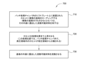
図7は、本開示の別の実施形態による、バッチ処理チャンバ内に配置された複数の基板を処理するための方法のブロック図である。方法700は、ブロック710において、リフトプレート上に配置されたカセットに、複数の基板をローディングすることにより始まる。基板のうちの一又は複数は、その基板の外面に露出した流動可能材料を有する。カセット及びリフトプレートは、バッチ処理チャンバの、真空に維持されている内側チャンバ内に配置される。例えば(限定するわけではないが)、工程の全ての段階において、バッチ処理チャンバ内に配置され、かつ内側チャンバの高圧領域を部分的に取り囲んでいる外側チャンバは、真空条件に維持される。一部の実施形態では、基板は、内側チャンバに接続された基板移送ポートを通じて、カセットにローディングされる。カセットは、複数の基板を収容するための複数の基板ストレージスロットを有する。カセットの基板ストレージスロットの各々は、基板をそこにローディングするために基板移送ポートと位置を合わせるよう、定寸送りされる(indexed)。これと同時に、リフトプレート及びカセットは、カセットにローディングされた基板の温度上昇を開始して処理時間を短縮するために、予加熱されうる。カセットに基板がローディングされると、オプションで、高圧領域内での処理に先立って基板を湿潤処理するために、湿潤剤が注入ポートを通じて内側チャンバに導入されうる。
FIG. 7 is a block diagram of a method for processing multiple substrates arranged in a batch processing chamber according to another embodiment of the present disclosure; The
カセットに基板がローディングされるか、又は別様に処理の準備が整うと、ブロック720において、カセットは処理位置まで上昇する。この処理位置では、高圧領域内のカセットが、内側チャンバの中にある低圧領域から分離される。リフト機構は、内側チャンバの中で高圧領域が分離されるように、リフトプレート及びリフトプレート上に配置されたカセットを処理位置まで上昇させるために、使用される。
Once the cassette is loaded with substrates or otherwise ready for processing, at
高圧領域が低圧領域から分離されると、ブロック730において、高圧領域の真空条件が高圧条件に置き換えられる。基板を処理流体に曝露すること、及び、高圧領域内の処理流体を蒸気相に維持する圧力及び温度まで高圧領域を加圧し加熱することによって、基板上に配置された流動可能材料が基板表面全体に再分配される。一例では、高圧領域は約10~約60バールの圧力まで加圧され、基板は摂氏約225度を上回る温度に加熱される。外側チャンバ内に配置されたヒータと、オプションでカセットを支持するリフトプレートとインターフェース接続された加熱素子を用いて、内側チャンバ内の高圧領域を摂氏約250度を上回る温度(例えば摂氏約300度~摂氏約450度)に維持することによって、基板は加熱される。処理流体は、注入ポートを通じてバッチ処理チャンバに導入される。一部の実施形態では、処理流体は水蒸気又は水でありうる。例えば、水蒸気は乾燥水蒸気でありうる。別の例では、水蒸気は、チャンバへの流入前に或いはチャンバ内で、例えばヒータによって過熱される。処理流体は、内側チャンバの一又は複数の出口ポートを通じて除去される。基板が処理される際に、基板表面上に露出した流動可能材料が再分配されて、基板に形成された間隙及びトレンチを充填する。
Once the high pressure region is separated from the low pressure region, at
処理後に、高圧領域内部の圧力は真空まで低減される。内側チャンバはオプションで冷却されてよく、注入ポートは閉ざされる。高圧領域が真空条件まで排気されると、カセットが上に配置されているリフトプレートは下降して、高圧領域と低圧領域との間の流体連結が可能になる。この時点で真空下にある処理済みの基板は、基板移送ポートを通じてバッチ処理チャンバから取り出される。基板が取り出された後に、内側チャンバ内に存在する不純物と反応して揮発性生成物及び副生成物を形成するラジカルが遠隔プラズマ源から流されることによって、バッチ処理チャンバは洗浄される。その後、これらの揮発性生成物及び副生成物は、内側チャンバから吸い出され(pumped out)、除去される。ゆえに、バッチ処理チャンバは、基板の次のバッチの処理に備えて準備される。 After processing, the pressure inside the high pressure region is reduced to vacuum. The inner chamber may optionally be cooled and the injection port closed. When the high pressure area is evacuated to vacuum conditions, the lift plate on which the cassette is placed is lowered to allow fluid communication between the high pressure area and the low pressure area. The processed substrate, now under vacuum, is removed from the batch processing chamber through the substrate transfer port. After the substrate is removed, the batch processing chamber is cleaned by flowing radicals from the remote plasma source that react with impurities present in the inner chamber to form volatile products and byproducts. These volatile products and by-products are then pumped out of the inner chamber and removed. Thus, the batch processing chamber is ready for processing the next batch of substrates.
バッチ処理チャンバ、及び、このバッチ処理チャンバ内で複数の基板を処理するための方法により、高圧及び高温のもとで複数の基板を処理することが可能になる。本開示のアーキテクチャは、処理中に高圧領域と低圧領域とを分離させると共に、低圧領域を真空に保つことによって、バッチ処理チャンバの内側チャンバ内での分離を有利に作り出す。基板は、分離が解消されている時に、カセットにローディングされ、カセットからアンローディング(取り外し)される。この分離により、2つの個別の環境(一方は高圧領域における処理のための環境であり、他方は低圧領域における基板のローディング/アンローディングのための環境である)の間の、熱分離が可能になる。更に、分離により、処理中に高圧領域を封止状態に保つことによって、チャンバの構成要素間の熱的不整合が防止される。 SUMMARY A batch processing chamber and method for processing multiple substrates in the batch processing chamber enables processing of multiple substrates under high pressure and temperature. The architecture of the present disclosure advantageously creates isolation within the inner chamber of the batch processing chamber by separating the high and low pressure regions during processing and keeping the low pressure region under vacuum. Substrates are loaded into and unloaded from the cassette when the separation is resolved. This separation allows for thermal isolation between two separate environments, one for processing in the high pressure region and the other for loading/unloading substrates in the low pressure region. Become. Further, the isolation prevents thermal mismatch between chamber components by keeping the high pressure region sealed during processing.
内側チャンバの高圧領域の周りに配置された外側チャンバであって、連続して真空に維持される外側チャンバは、追加的に、処理環境内への空気のいかなる漏れも、チャンバ外部の大気への処理流体のいかなる損失も防止するために、内側チャンバ内部の高圧領域の処理環境と、バッチ処理チャンバ外部の大気との間の安全閉じ込め装置(safety containment)としても機能する。更に、外側チャンバは真空に維持され、かつバッチ処理チャンバ外部の大気から分離されているので、外側チャンバ内に設置されるヒータであって、内側チャンバを加熱するよう構成されるヒータを選択する上での、柔軟性を供する。ゆえに、真空条件下でより有効に機能するヒータが利用されうる。 An outer chamber disposed about the high pressure region of the inner chamber and maintained at a continuous vacuum additionally prevents any leakage of air into the processing environment from entering the atmosphere outside the chamber. It also serves as a safety containment between the high pressure region processing environment inside the inner chamber and the atmosphere outside the batch processing chamber to prevent any loss of process fluid. Further, since the outer chamber is maintained at a vacuum and is isolated from the atmosphere outside the batch processing chamber, a heater located within the outer chamber and configured to heat the inner chamber is selected. provide flexibility in Therefore, heaters that function more effectively under vacuum conditions can be utilized.
上述のバッチ処理チャンバは、追加的に、スタンドアロンプロセスチャンバ若しくはクラスタツール内のファクトリインターフェースにドッキングされるチャンバとして動作可能であり、プロセスチャンバの一部としてインシトゥ(in-situ)でも動作可能であるという、柔軟性も供する。これにより、基板を処理するために維持されうる、クリーンルームレベルの環境が確保される。 The batch processing chamber described above can additionally operate as a stand-alone process chamber or a chamber docked to a factory interface in a cluster tool, and can operate in-situ as part of a process chamber. , also provides flexibility. This ensures a clean room level environment that can be maintained for processing substrates.
本明細書の記載は本開示の特定の実施形態を対象としているが、これらの実施形態は、本発明の原理及び応用の単なる例示であることを理解されたい。したがって、付随する特許請求の範囲により規定されている本発明の本質及び範囲から逸脱しなければ、例示的な実施形態には、他の実施形態に到達するよう多数の改変がなされうることを、理解すべきである。 Although the description herein is directed to specific embodiments of the disclosure, it is to be understood that these embodiments are merely illustrative of the principles and applications of the invention. Accordingly, it should be appreciated that many modifications may be made to the illustrative embodiments to arrive at other embodiments without departing from the spirit and scope of the invention as defined by the appended claims. should understand.
Claims (18)
前記下側シェルを通って形成された基板移送ポートと、
前記下側シェルの上に配置された上側シェルと、
前記上側シェルの中に配置された内側シェルであって、内側シェルと前記上側シェルが外側チャンバを囲んでおり、内側シェルと前記下側シェルが、前記外側チャンバから分離されている内側チャンバを囲んでいる、内側シェルと、
前記内側シェルを加熱するよう動作可能なヒータと、
前記下側シェルの中に可動式に配置されたリフトプレートであって、リフトプレートが、上昇位置にある時に、前記内側チャンバを高圧領域と低圧領域とに密封分離させ、前記高圧領域がリフトプレート及び前記内側シェルに囲まれる、リフトプレートと、
前記リフトプレートの上に配置されたカセットであって、複数の基板を保持するよう構成されたカセットと、
前記内側チャンバに流体を導入するよう構成された注入ポートと、
前記内側シェルの底面に取り外し可能に連結された注入リングと、
前記リフトプレートが上昇位置にある時に前記注入リングを前記リフトプレートに密封するよう構成された、高圧シールと、
前記高圧シールと前記内側シェルとの間であって、前記注入リング内に配置された冷却チャネルとを備える、
バッチ処理チャンバ。 a lower shell;
a substrate transfer port formed through the lower shell;
an upper shell positioned over the lower shell;
an inner shell disposed within said upper shell, said inner shell and said upper shell surrounding an outer chamber, and said inner shell and said lower shell surrounding an inner chamber separated from said outer chamber; with an inner shell and
a heater operable to heat the inner shell;
a lift plate movably disposed within the lower shell, sealingly separating the inner chamber into a high pressure region and a low pressure region when the lift plate is in a raised position, the high pressure region being the lift plate; and a lift plate surrounded by the inner shell;
a cassette positioned above the lift plate and configured to hold a plurality of substrates;
an injection port configured to introduce fluid into the inner chamber ;
an injection ring removably coupled to the bottom surface of the inner shell;
a high pressure seal configured to seal the injection ring to the lift plate when the lift plate is in the raised position;
a cooling channel disposed within the injection ring between the high pressure seal and the inner shell ;
batch processing chamber.
前記下側シェルを通って形成された基板移送ポートと、
前記下側シェルの底面に連結された底部プレートと、
前記下側シェルの上に配置された上側シェルと、
前記上側シェルの中に配置された内側シェルであって、高圧領域と低圧領域とを有する内側チャンバの一部分を囲んでいる、内側シェルと
前記内側シェルと前記上側シェルに囲まれた外側チャンバであって、前記内側チャンバから分離された外側チャンバと、
前記外側チャンバ内に配置された一又は複数のヒータであって、前記内側シェルを加熱するよう動作可能な、一又は複数のヒータと、
前記下側シェルの中に可動式に配置されたリフトプレートであって、上昇して前記高圧領域を密封し、下降して、前記高圧領域と前記低圧領域との間の流体連結を可能にするよう構成された、リフトプレートと、
前記リフトプレートに連結された加熱素子と、
前記リフトプレートの上に配置されたカセットであって、複数の基板を保持するよう構成されたカセットと、
前記内側シェルの底面に取り外し可能に連結された注入リングと、
前記注入リングの中に配置された注入ポートであって、前記内側チャンバに流体を導入するよう構成された注入ポートと、
前記高圧領域において前記注入リングと前記リフトプレートとを連結するよう構成された、高圧シールと、
前記高圧シールと前記内側シェルとの間であって、前記注入リング内に配置された冷却チャネルと、
前記注入リングを通って形成された一又は複数の出口ポートであって、前記内側チャンバを横切って前記注入ポートに面している、一又は複数の出口ポートと、
前記内側チャンバに連結された遠隔プラズマ源とを備える、
バッチ処理チャンバ。 a lower shell;
a substrate transfer port formed through the lower shell;
a bottom plate connected to the bottom surface of the lower shell;
an upper shell positioned over the lower shell;
an inner shell disposed within the upper shell and surrounding a portion of the inner chamber having a high pressure region and a low pressure region; and an outer chamber bounded by the inner shell and the upper shell. an outer chamber separated from the inner chamber;
one or more heaters disposed within the outer chamber and operable to heat the inner shell;
A lift plate movably disposed within the lower shell that rises to seal the high pressure region and lowers to allow fluid communication between the high pressure region and the low pressure region. a lift plate configured to:
a heating element coupled to the lift plate;
a cassette positioned above the lift plate and configured to hold a plurality of substrates;
an injection ring removably coupled to the bottom surface of the inner shell;
an injection port disposed within the injection ring, the injection port configured to introduce fluid into the inner chamber;
a high pressure seal configured to connect the injection ring and the lift plate at the high pressure region;
a cooling channel disposed within the injection ring between the high pressure seal and the inner shell ;
one or more exit ports formed through the injection ring, one or more exit ports across the inner chamber facing the injection port;
a remote plasma source coupled to the inner chamber;
batch processing chamber.
リフトプレート上に配置されたカセットに複数の基板を装填することであって、前記カセット及び前記リフトプレートが前記バッチ処理チャンバの内側チャンバ内に配置され、装填される前の前記複数の基板のうちの少なくとも第1の基板が、前記基板の外面に露出した流動可能材料を有する、複数の基板を装填することと、
処理位置まで前記カセットを上昇させることであって、前記処理位置では、前記内側チャンバの高圧領域内の前記カセットが、前記内側チャンバの低圧領域から分離される、前記カセットを上昇させることと、
前記第1の基板の前記外面に露出した前記流動可能材料を流動させることであって、
前記第1の基板を、前記高圧領域の中にある時に、処理流体を蒸気相に維持する温度及び圧力において、前記処理流体に曝露することを更に含む、前記流動可能材料を流動させることとを含む、
方法。 A method of processing a plurality of substrates arranged in a batch processing chamber, comprising:
loading a plurality of substrates into a cassette arranged on a lift plate, wherein the cassette and the lift plate are arranged in an inner chamber of the batch processing chamber and one of the plurality of substrates before being loaded; loading a plurality of substrates, wherein at least a first substrate of has flowable material exposed on an outer surface of said substrate;
raising the cassette to a processing position in which the cassette in the high pressure region of the inner chamber is separated from the low pressure region of the inner chamber;
Flowing the flowable material exposed on the outer surface of the first substrate, comprising:
flowing the flowable material, further comprising exposing the first substrate to the processing fluid at a temperature and pressure that maintains the processing fluid in a vapor phase while in the high pressure region; include,
Method.
前記第1の基板を水蒸気又は水に曝露することを含む、請求項10に記載の方法。 exposing the first substrate to the process fluid;
11. The method of claim 10 , comprising exposing the first substrate to water vapor or water.
Applications Claiming Priority (3)
| Application Number | Priority Date | Filing Date | Title |
|---|---|---|---|
| US201762492700P | 2017-05-01 | 2017-05-01 | |
| US62/492,700 | 2017-05-01 | ||
| PCT/US2018/028258 WO2018204078A1 (en) | 2017-05-01 | 2018-04-19 | High pressure anneal chamber with vacuum isolation and pre-processing environment |
Publications (3)
| Publication Number | Publication Date |
|---|---|
| JP2020519018A JP2020519018A (en) | 2020-06-25 |
| JP2020519018A5 JP2020519018A5 (en) | 2021-05-27 |
| JP7235678B2 true JP7235678B2 (en) | 2023-03-08 |
Family
ID=63917378
Family Applications (1)
| Application Number | Title | Priority Date | Filing Date |
|---|---|---|---|
| JP2019559058A Active JP7235678B2 (en) | 2017-05-01 | 2018-04-19 | High pressure annealing chamber with vacuum isolation and pretreatment environment |
Country Status (6)
| Country | Link |
|---|---|
| US (1) | US20180315626A1 (en) |
| JP (1) | JP7235678B2 (en) |
| KR (1) | KR20190137935A (en) |
| CN (2) | CN116504679A (en) |
| TW (1) | TW201842590A (en) |
| WO (1) | WO2018204078A1 (en) |
Cited By (1)
| Publication number | Priority date | Publication date | Assignee | Title |
|---|---|---|---|---|
| KR20200075009A (en) * | 2017-11-16 | 2020-06-25 | 어플라이드 머티어리얼스, 인코포레이티드 | High pressure steam annealing processing device |
Families Citing this family (27)
| Publication number | Priority date | Publication date | Assignee | Title |
|---|---|---|---|---|
| JP5541274B2 (en) * | 2011-12-28 | 2014-07-09 | 東京エレクトロン株式会社 | Substrate processing apparatus, substrate processing method, and storage medium |
| JP6054470B2 (en) | 2015-05-26 | 2016-12-27 | 株式会社日本製鋼所 | Atomic layer growth equipment |
| JP6050860B1 (en) * | 2015-05-26 | 2016-12-21 | 株式会社日本製鋼所 | Plasma atomic layer growth equipment |
| JP6054471B2 (en) | 2015-05-26 | 2016-12-27 | 株式会社日本製鋼所 | Atomic layer growth apparatus and exhaust layer of atomic layer growth apparatus |
| US10622214B2 (en) | 2017-05-25 | 2020-04-14 | Applied Materials, Inc. | Tungsten defluorination by high pressure treatment |
| JP6947914B2 (en) | 2017-08-18 | 2021-10-13 | アプライド マテリアルズ インコーポレイテッドApplied Materials,Incorporated | Annealing chamber under high pressure and high temperature |
| US10276411B2 (en) | 2017-08-18 | 2019-04-30 | Applied Materials, Inc. | High pressure and high temperature anneal chamber |
| JP7274461B2 (en) | 2017-09-12 | 2023-05-16 | アプライド マテリアルズ インコーポレイテッド | Apparatus and method for manufacturing semiconductor structures using protective barrier layers |
| EP3707746B1 (en) | 2017-11-11 | 2023-12-27 | Micromaterials LLC | Gas delivery system for high pressure processing chamber |
| JP2021503714A (en) | 2017-11-17 | 2021-02-12 | アプライド マテリアルズ インコーポレイテッドApplied Materials,Incorporated | Capacitor system for high pressure processing system |
| KR20230079236A (en) | 2018-03-09 | 2023-06-05 | 어플라이드 머티어리얼스, 인코포레이티드 | High pressure annealing process for metal containing materials |
| US10714331B2 (en) | 2018-04-04 | 2020-07-14 | Applied Materials, Inc. | Method to fabricate thermally stable low K-FinFET spacer |
| US10950429B2 (en) | 2018-05-08 | 2021-03-16 | Applied Materials, Inc. | Methods of forming amorphous carbon hard mask layers and hard mask layers formed therefrom |
| US10748783B2 (en) | 2018-07-25 | 2020-08-18 | Applied Materials, Inc. | Gas delivery module |
| US10675581B2 (en) | 2018-08-06 | 2020-06-09 | Applied Materials, Inc. | Gas abatement apparatus |
| JP7179172B6 (en) | 2018-10-30 | 2022-12-16 | アプライド マテリアルズ インコーポレイテッド | Method for etching structures for semiconductor applications |
| SG11202103763QA (en) | 2018-11-16 | 2021-05-28 | Applied Materials Inc | Film deposition using enhanced diffusion process |
| TWI738002B (en) * | 2018-12-05 | 2021-09-01 | 洪義明 | Temperature adjustment equipment of high temperature oven |
| WO2020117462A1 (en) | 2018-12-07 | 2020-06-11 | Applied Materials, Inc. | Semiconductor processing system |
| WO2020156660A1 (en) * | 2019-01-30 | 2020-08-06 | Applied Materials, Inc. | Method for cleaning a vacuum system, method for vacuum processing of a substrate, and apparatus for vacuum processing a substrate |
| CN110133969A (en) * | 2019-04-26 | 2019-08-16 | 厦门通富微电子有限公司 | It is a kind of for toasting the roasting plant, baking system and baking method of photoresist |
| US11631571B2 (en) | 2019-08-12 | 2023-04-18 | Kurt J. Lesker Company | Ultra high purity conditions for atomic scale processing |
| JP2023507327A (en) * | 2019-12-20 | 2023-02-22 | アプライド マテリアルズ インコーポレイテッド | Baking equipment for substrate handling and uniform baking |
| FI129609B (en) * | 2020-01-10 | 2022-05-31 | Picosun Oy | Substrate processing apparatus |
| US11901222B2 (en) | 2020-02-17 | 2024-02-13 | Applied Materials, Inc. | Multi-step process for flowable gap-fill film |
| US20210398824A1 (en) * | 2020-06-19 | 2021-12-23 | Applied Materials, Inc. | Batch wafer degas chamber and integration into factory interface and vacuum-based mainframe |
| US20240120220A1 (en) * | 2022-10-06 | 2024-04-11 | Applied Materials, Inc. | Load lock chambers and related methods and structures for batch cooling or heating |
Citations (6)
| Publication number | Priority date | Publication date | Assignee | Title |
|---|---|---|---|---|
| JP2007180331A (en) | 2005-12-28 | 2007-07-12 | Ishikawajima Harima Heavy Ind Co Ltd | Heat treatment device |
| JP2007242785A (en) | 2006-03-07 | 2007-09-20 | Ihi Corp | Heat treatment apparatus and heat treatment method |
| JP2013084643A (en) | 2011-10-06 | 2013-05-09 | Nano Material Kenkyusho:Kk | Semiconductor manufacturing device, and manufacturing method |
| JP2014512687A (en) | 2011-04-20 | 2014-05-22 | アプライド マテリアルズ インコーポレイテッド | Low temperature silicon oxide conversion |
| JP2015530477A (en) | 2012-06-27 | 2015-10-15 | イノシティ カンパニー リミテッド | Substrate heating apparatus and process chamber |
| JP2016526279A (en) | 2013-04-30 | 2016-09-01 | アプライド マテリアルズ インコーポレイテッドApplied Materials,Incorporated | Flow control liner with spatially dispersed gas flow paths |
Family Cites Families (10)
| Publication number | Priority date | Publication date | Assignee | Title |
|---|---|---|---|---|
| JP2766856B2 (en) * | 1988-11-11 | 1998-06-18 | 東京エレクトロン株式会社 | Vertical pressure oxidation equipment |
| JP3471100B2 (en) * | 1994-11-07 | 2003-11-25 | 東京エレクトロン株式会社 | Vertical heat treatment equipment |
| JP3445148B2 (en) * | 1998-05-21 | 2003-09-08 | 株式会社神戸製鋼所 | High-temperature and high-pressure processing equipment for substrates to be processed |
| JP4207354B2 (en) * | 2000-03-07 | 2009-01-14 | 東京エレクトロン株式会社 | Heat treatment apparatus and operation method thereof |
| JP2003077974A (en) * | 2001-08-31 | 2003-03-14 | Hitachi Kokusai Electric Inc | Substrate processing device and manufacturing method of semiconductor device |
| US20040060519A1 (en) * | 2002-10-01 | 2004-04-01 | Seh America Inc. | Quartz to quartz seal using expanded PTFE gasket material |
| JP4456341B2 (en) * | 2003-06-30 | 2010-04-28 | 株式会社日立国際電気 | Semiconductor device manufacturing method and substrate processing apparatus |
| US7158221B2 (en) * | 2003-12-23 | 2007-01-02 | Applied Materials, Inc. | Method and apparatus for performing limited area spectral analysis |
| US20060156979A1 (en) * | 2004-11-22 | 2006-07-20 | Applied Materials, Inc. | Substrate processing apparatus using a batch processing chamber |
| WO2014192871A1 (en) * | 2013-05-31 | 2014-12-04 | 株式会社日立国際電気 | Substrate processing apparatus, method for manufacturing semiconductor manufacturing apparatus, and furnace opening cover body |
-
2018
- 2018-04-19 CN CN202310566128.3A patent/CN116504679A/en active Pending
- 2018-04-19 TW TW107113314A patent/TW201842590A/en unknown
- 2018-04-19 JP JP2019559058A patent/JP7235678B2/en active Active
- 2018-04-19 KR KR1020197035331A patent/KR20190137935A/en not_active Application Discontinuation
- 2018-04-19 CN CN201880028790.0A patent/CN110574150B/en active Active
- 2018-04-19 WO PCT/US2018/028258 patent/WO2018204078A1/en active Application Filing
- 2018-04-27 US US15/964,300 patent/US20180315626A1/en not_active Abandoned
Patent Citations (6)
| Publication number | Priority date | Publication date | Assignee | Title |
|---|---|---|---|---|
| JP2007180331A (en) | 2005-12-28 | 2007-07-12 | Ishikawajima Harima Heavy Ind Co Ltd | Heat treatment device |
| JP2007242785A (en) | 2006-03-07 | 2007-09-20 | Ihi Corp | Heat treatment apparatus and heat treatment method |
| JP2014512687A (en) | 2011-04-20 | 2014-05-22 | アプライド マテリアルズ インコーポレイテッド | Low temperature silicon oxide conversion |
| JP2013084643A (en) | 2011-10-06 | 2013-05-09 | Nano Material Kenkyusho:Kk | Semiconductor manufacturing device, and manufacturing method |
| JP2015530477A (en) | 2012-06-27 | 2015-10-15 | イノシティ カンパニー リミテッド | Substrate heating apparatus and process chamber |
| JP2016526279A (en) | 2013-04-30 | 2016-09-01 | アプライド マテリアルズ インコーポレイテッドApplied Materials,Incorporated | Flow control liner with spatially dispersed gas flow paths |
Cited By (2)
| Publication number | Priority date | Publication date | Assignee | Title |
|---|---|---|---|---|
| KR20200075009A (en) * | 2017-11-16 | 2020-06-25 | 어플라이드 머티어리얼스, 인코포레이티드 | High pressure steam annealing processing device |
| KR102622303B1 (en) | 2017-11-16 | 2024-01-05 | 어플라이드 머티어리얼스, 인코포레이티드 | High pressure steam annealing processing equipment |
Also Published As
| Publication number | Publication date |
|---|---|
| CN116504679A (en) | 2023-07-28 |
| KR20190137935A (en) | 2019-12-11 |
| US20180315626A1 (en) | 2018-11-01 |
| TW201842590A (en) | 2018-12-01 |
| WO2018204078A1 (en) | 2018-11-08 |
| JP2020519018A (en) | 2020-06-25 |
| CN110574150A (en) | 2019-12-13 |
| CN110574150B (en) | 2023-09-19 |
Similar Documents
| Publication | Publication Date | Title |
|---|---|---|
| JP7235678B2 (en) | High pressure annealing chamber with vacuum isolation and pretreatment environment | |
| US20220275515A1 (en) | Substrate processing apparatus and method of manufacturing semiconductor device | |
| JP7184810B6 (en) | Improving the quality of films deposited on substrates | |
| US7993457B1 (en) | Deposition sub-chamber with variable flow | |
| TWI489003B (en) | Processing chamber with heated chamber liner | |
| KR101356445B1 (en) | Vertical film formation apparatus, method for using same, and storage medium | |
| JP5632687B2 (en) | Semiconductor device manufacturing method and substrate processing apparatus | |
| KR20200002622A (en) | Temperature-controlled flange and reactor system including same | |
| CN109585248B (en) | Method and apparatus for in-situ cleaning of a process chamber | |
| KR20070121756A (en) | Substrate processing platform allowing processing in different ambients | |
| JP2013530536A (en) | Load lock batch ozone curing | |
| JP2007525021A (en) | Gas distribution shower head featuring exhaust aperture | |
| JP6793031B2 (en) | Substrate processing equipment and substrate processing method, and substrate processing system | |
| US11952664B2 (en) | Substrate processing apparatus and method of manufacturing semiconductor device | |
| JP6976043B2 (en) | Systems and methods that enable low defect treatment by controlled separation and delivery of chemicals during atomic layer deposition | |
| TWI807192B (en) | Gas introduction structure, heat treatment device, and gas supply method | |
| JP2008255386A (en) | Substrate treatment device | |
| CN112996950B (en) | Film deposition using enhanced diffusion process | |
| EP1209250A1 (en) | Apparatus for cleaning a semiconductor process chamber | |
| JP6472356B2 (en) | Heat treatment equipment | |
| JP5571157B2 (en) | Semiconductor device manufacturing method, cleaning method, and substrate processing apparatus |
Legal Events
| Date | Code | Title | Description |
|---|---|---|---|
| A521 | Request for written amendment filed |
Free format text: JAPANESE INTERMEDIATE CODE: A523 Effective date: 20210419 |
|
| A621 | Written request for application examination |
Free format text: JAPANESE INTERMEDIATE CODE: A621 Effective date: 20210419 |
|
| A977 | Report on retrieval |
Free format text: JAPANESE INTERMEDIATE CODE: A971007 Effective date: 20220531 |
|
| A131 | Notification of reasons for refusal |
Free format text: JAPANESE INTERMEDIATE CODE: A131 Effective date: 20220621 |
|
| A521 | Request for written amendment filed |
Free format text: JAPANESE INTERMEDIATE CODE: A523 Effective date: 20220921 |
|
| TRDD | Decision of grant or rejection written | ||
| A01 | Written decision to grant a patent or to grant a registration (utility model) |
Free format text: JAPANESE INTERMEDIATE CODE: A01 Effective date: 20230131 |
|
| A61 | First payment of annual fees (during grant procedure) |
Free format text: JAPANESE INTERMEDIATE CODE: A61 Effective date: 20230224 |
|
| R150 | Certificate of patent or registration of utility model |
Ref document number: 7235678 Country of ref document: JP Free format text: JAPANESE INTERMEDIATE CODE: R150 |