JP7231066B2 - Semiconductor device and method for manufacturing semiconductor device - Google Patents
Semiconductor device and method for manufacturing semiconductor device Download PDFInfo
- Publication number
- JP7231066B2 JP7231066B2 JP2021571240A JP2021571240A JP7231066B2 JP 7231066 B2 JP7231066 B2 JP 7231066B2 JP 2021571240 A JP2021571240 A JP 2021571240A JP 2021571240 A JP2021571240 A JP 2021571240A JP 7231066 B2 JP7231066 B2 JP 7231066B2
- Authority
- JP
- Japan
- Prior art keywords
- region
- concentration
- semiconductor substrate
- hydrogen
- depth position
- Prior art date
- Legal status (The legal status is an assumption and is not a legal conclusion. Google has not performed a legal analysis and makes no representation as to the accuracy of the status listed.)
- Active
Links
- 239000004065 semiconductor Substances 0.000 title claims description 310
- 238000000034 method Methods 0.000 title claims description 44
- 238000004519 manufacturing process Methods 0.000 title claims description 30
- 229910052739 hydrogen Inorganic materials 0.000 claims description 238
- 239000001257 hydrogen Substances 0.000 claims description 238
- 239000000758 substrate Substances 0.000 claims description 216
- UFHFLCQGNIYNRP-UHFFFAOYSA-N Hydrogen Chemical compound [H][H] UFHFLCQGNIYNRP-UHFFFAOYSA-N 0.000 claims description 163
- 239000000126 substance Substances 0.000 claims description 158
- 230000006798 recombination Effects 0.000 claims description 120
- -1 hydrogen ions Chemical class 0.000 claims description 77
- 238000009826 distribution Methods 0.000 claims description 55
- 238000005215 recombination Methods 0.000 claims description 53
- 239000002245 particle Substances 0.000 claims description 52
- 238000010438 heat treatment Methods 0.000 claims description 38
- 239000001307 helium Substances 0.000 claims description 30
- 229910052734 helium Inorganic materials 0.000 claims description 30
- 238000002513 implantation Methods 0.000 claims description 26
- SWQJXJOGLNCZEY-UHFFFAOYSA-N helium atom Chemical group [He] SWQJXJOGLNCZEY-UHFFFAOYSA-N 0.000 claims description 23
- 239000002019 doping agent Substances 0.000 claims description 19
- 238000000227 grinding Methods 0.000 claims description 16
- 239000012535 impurity Substances 0.000 claims description 16
- 230000007423 decrease Effects 0.000 claims description 8
- 238000007669 thermal treatment Methods 0.000 claims 1
- 238000010586 diagram Methods 0.000 description 32
- 238000002347 injection Methods 0.000 description 31
- 239000007924 injection Substances 0.000 description 31
- 239000000386 donor Substances 0.000 description 29
- 239000000370 acceptor Substances 0.000 description 28
- OAICVXFJPJFONN-UHFFFAOYSA-N Phosphorus Chemical compound [P] OAICVXFJPJFONN-UHFFFAOYSA-N 0.000 description 19
- 239000011229 interlayer Substances 0.000 description 19
- 229910052698 phosphorus Inorganic materials 0.000 description 19
- 239000011574 phosphorus Substances 0.000 description 19
- 230000007547 defect Effects 0.000 description 15
- 238000009825 accumulation Methods 0.000 description 13
- 230000002093 peripheral effect Effects 0.000 description 12
- 239000000852 hydrogen donor Substances 0.000 description 10
- 150000002500 ions Chemical class 0.000 description 8
- QVGXLLKOCUKJST-UHFFFAOYSA-N atomic oxygen Chemical compound [O] QVGXLLKOCUKJST-UHFFFAOYSA-N 0.000 description 7
- 229910052760 oxygen Inorganic materials 0.000 description 7
- 239000001301 oxygen Substances 0.000 description 7
- 229910052782 aluminium Inorganic materials 0.000 description 6
- XAGFODPZIPBFFR-UHFFFAOYSA-N aluminium Chemical compound [Al] XAGFODPZIPBFFR-UHFFFAOYSA-N 0.000 description 6
- 230000015572 biosynthetic process Effects 0.000 description 6
- FMGSKLZLMKYGDP-USOAJAOKSA-N dehydroepiandrosterone Chemical compound C1[C@@H](O)CC[C@]2(C)[C@H]3CC[C@](C)(C(CC4)=O)[C@@H]4[C@@H]3CC=C21 FMGSKLZLMKYGDP-USOAJAOKSA-N 0.000 description 6
- 239000010410 layer Substances 0.000 description 6
- 230000008569 process Effects 0.000 description 6
- 125000004429 atom Chemical group 0.000 description 5
- BHEPBYXIRTUNPN-UHFFFAOYSA-N hydridophosphorus(.) (triplet) Chemical compound [PH] BHEPBYXIRTUNPN-UHFFFAOYSA-N 0.000 description 5
- ZOXJGFHDIHLPTG-UHFFFAOYSA-N Boron Chemical compound [B] ZOXJGFHDIHLPTG-UHFFFAOYSA-N 0.000 description 4
- 229910052796 boron Inorganic materials 0.000 description 4
- 239000000969 carrier Substances 0.000 description 4
- 150000002431 hydrogen Chemical class 0.000 description 4
- 229910052751 metal Inorganic materials 0.000 description 4
- 239000002184 metal Substances 0.000 description 4
- 239000007769 metal material Substances 0.000 description 4
- 229910021420 polycrystalline silicon Inorganic materials 0.000 description 4
- 229920005591 polysilicon Polymers 0.000 description 4
- XUIMIQQOPSSXEZ-UHFFFAOYSA-N Silicon Chemical compound [Si] XUIMIQQOPSSXEZ-UHFFFAOYSA-N 0.000 description 3
- 230000001133 acceleration Effects 0.000 description 3
- 230000005684 electric field Effects 0.000 description 3
- 239000000463 material Substances 0.000 description 3
- 229920002120 photoresistant polymer Polymers 0.000 description 3
- 238000001004 secondary ion mass spectrometry Methods 0.000 description 3
- 229910052710 silicon Inorganic materials 0.000 description 3
- 239000010703 silicon Substances 0.000 description 3
- WFKWXMTUELFFGS-UHFFFAOYSA-N tungsten Chemical compound [W] WFKWXMTUELFFGS-UHFFFAOYSA-N 0.000 description 3
- 229910052721 tungsten Inorganic materials 0.000 description 3
- 239000010937 tungsten Substances 0.000 description 3
- BUGBHKTXTAQXES-UHFFFAOYSA-N Selenium Chemical compound [Se] BUGBHKTXTAQXES-UHFFFAOYSA-N 0.000 description 2
- 229910052785 arsenic Inorganic materials 0.000 description 2
- RQNWIZPPADIBDY-UHFFFAOYSA-N arsenic atom Chemical compound [As] RQNWIZPPADIBDY-UHFFFAOYSA-N 0.000 description 2
- 230000004888 barrier function Effects 0.000 description 2
- 230000015556 catabolic process Effects 0.000 description 2
- 239000004020 conductor Substances 0.000 description 2
- 239000013078 crystal Substances 0.000 description 2
- 238000009792 diffusion process Methods 0.000 description 2
- 230000000694 effects Effects 0.000 description 2
- 238000010894 electron beam technology Methods 0.000 description 2
- 230000001747 exhibiting effect Effects 0.000 description 2
- GPRLSGONYQIRFK-UHFFFAOYSA-N hydron Chemical compound [H+] GPRLSGONYQIRFK-UHFFFAOYSA-N 0.000 description 2
- 238000005468 ion implantation Methods 0.000 description 2
- 230000004048 modification Effects 0.000 description 2
- 238000012986 modification Methods 0.000 description 2
- 230000003647 oxidation Effects 0.000 description 2
- 238000007254 oxidation reaction Methods 0.000 description 2
- 238000011084 recovery Methods 0.000 description 2
- 229910052711 selenium Inorganic materials 0.000 description 2
- 239000011669 selenium Substances 0.000 description 2
- 230000007480 spreading Effects 0.000 description 2
- 238000003892 spreading Methods 0.000 description 2
- 229910000789 Aluminium-silicon alloy Inorganic materials 0.000 description 1
- 229910000676 Si alloy Inorganic materials 0.000 description 1
- NINIDFKCEFEMDL-UHFFFAOYSA-N Sulfur Chemical compound [S] NINIDFKCEFEMDL-UHFFFAOYSA-N 0.000 description 1
- RTAQQCXQSZGOHL-UHFFFAOYSA-N Titanium Chemical compound [Ti] RTAQQCXQSZGOHL-UHFFFAOYSA-N 0.000 description 1
- KPSZQYZCNSCYGG-UHFFFAOYSA-N [B].[B] Chemical compound [B].[B] KPSZQYZCNSCYGG-UHFFFAOYSA-N 0.000 description 1
- 230000004913 activation Effects 0.000 description 1
- CSDREXVUYHZDNP-UHFFFAOYSA-N alumanylidynesilicon Chemical compound [Al].[Si] CSDREXVUYHZDNP-UHFFFAOYSA-N 0.000 description 1
- 238000000137 annealing Methods 0.000 description 1
- 229910052787 antimony Inorganic materials 0.000 description 1
- WATWJIUSRGPENY-UHFFFAOYSA-N antimony atom Chemical compound [Sb] WATWJIUSRGPENY-UHFFFAOYSA-N 0.000 description 1
- 238000004364 calculation method Methods 0.000 description 1
- 230000008859 change Effects 0.000 description 1
- 230000005484 gravity Effects 0.000 description 1
- 125000004435 hydrogen atom Chemical group [H]* 0.000 description 1
- 238000005224 laser annealing Methods 0.000 description 1
- 238000005259 measurement Methods 0.000 description 1
- 238000000691 measurement method Methods 0.000 description 1
- 229910001092 metal group alloy Inorganic materials 0.000 description 1
- 238000005121 nitriding Methods 0.000 description 1
- 230000001590 oxidative effect Effects 0.000 description 1
- 238000000059 patterning Methods 0.000 description 1
- 230000001737 promoting effect Effects 0.000 description 1
- 238000004904 shortening Methods 0.000 description 1
- 239000005368 silicate glass Substances 0.000 description 1
- 238000004088 simulation Methods 0.000 description 1
- 239000000243 solution Substances 0.000 description 1
- 229910052717 sulfur Inorganic materials 0.000 description 1
- 239000011593 sulfur Substances 0.000 description 1
- 239000002344 surface layer Substances 0.000 description 1
- 239000010936 titanium Substances 0.000 description 1
- 229910052719 titanium Inorganic materials 0.000 description 1
- 150000003609 titanium compounds Chemical class 0.000 description 1
- 229910052723 transition metal Inorganic materials 0.000 description 1
- 150000003624 transition metals Chemical class 0.000 description 1
Images


Classifications
-
- H—ELECTRICITY
- H01—ELECTRIC ELEMENTS
- H01L—SEMICONDUCTOR DEVICES NOT COVERED BY CLASS H10
- H01L27/00—Devices consisting of a plurality of semiconductor or other solid-state components formed in or on a common substrate
- H01L27/02—Devices consisting of a plurality of semiconductor or other solid-state components formed in or on a common substrate including semiconductor components specially adapted for rectifying, oscillating, amplifying or switching and having potential barriers; including integrated passive circuit elements having potential barriers
- H01L27/04—Devices consisting of a plurality of semiconductor or other solid-state components formed in or on a common substrate including semiconductor components specially adapted for rectifying, oscillating, amplifying or switching and having potential barriers; including integrated passive circuit elements having potential barriers the substrate being a semiconductor body
- H01L27/06—Devices consisting of a plurality of semiconductor or other solid-state components formed in or on a common substrate including semiconductor components specially adapted for rectifying, oscillating, amplifying or switching and having potential barriers; including integrated passive circuit elements having potential barriers the substrate being a semiconductor body including a plurality of individual components in a non-repetitive configuration
- H01L27/07—Devices consisting of a plurality of semiconductor or other solid-state components formed in or on a common substrate including semiconductor components specially adapted for rectifying, oscillating, amplifying or switching and having potential barriers; including integrated passive circuit elements having potential barriers the substrate being a semiconductor body including a plurality of individual components in a non-repetitive configuration the components having an active region in common
- H01L27/0705—Devices consisting of a plurality of semiconductor or other solid-state components formed in or on a common substrate including semiconductor components specially adapted for rectifying, oscillating, amplifying or switching and having potential barriers; including integrated passive circuit elements having potential barriers the substrate being a semiconductor body including a plurality of individual components in a non-repetitive configuration the components having an active region in common comprising components of the field effect type
- H01L27/0727—Devices consisting of a plurality of semiconductor or other solid-state components formed in or on a common substrate including semiconductor components specially adapted for rectifying, oscillating, amplifying or switching and having potential barriers; including integrated passive circuit elements having potential barriers the substrate being a semiconductor body including a plurality of individual components in a non-repetitive configuration the components having an active region in common comprising components of the field effect type in combination with diodes, or capacitors or resistors
-
- H—ELECTRICITY
- H01—ELECTRIC ELEMENTS
- H01L—SEMICONDUCTOR DEVICES NOT COVERED BY CLASS H10
- H01L29/00—Semiconductor devices specially adapted for rectifying, amplifying, oscillating or switching and having potential barriers; Capacitors or resistors having potential barriers, e.g. a PN-junction depletion layer or carrier concentration layer; Details of semiconductor bodies or of electrodes thereof ; Multistep manufacturing processes therefor
- H01L29/66—Types of semiconductor device ; Multistep manufacturing processes therefor
- H01L29/86—Types of semiconductor device ; Multistep manufacturing processes therefor controllable only by variation of the electric current supplied, or only the electric potential applied, to one or more of the electrodes carrying the current to be rectified, amplified, oscillated or switched
- H01L29/861—Diodes
- H01L29/8613—Mesa PN junction diodes
-
- H—ELECTRICITY
- H01—ELECTRIC ELEMENTS
- H01L—SEMICONDUCTOR DEVICES NOT COVERED BY CLASS H10
- H01L21/00—Processes or apparatus adapted for the manufacture or treatment of semiconductor or solid state devices or of parts thereof
- H01L21/02—Manufacture or treatment of semiconductor devices or of parts thereof
- H01L21/04—Manufacture or treatment of semiconductor devices or of parts thereof the devices having potential barriers, e.g. a PN junction, depletion layer or carrier concentration layer
- H01L21/18—Manufacture or treatment of semiconductor devices or of parts thereof the devices having potential barriers, e.g. a PN junction, depletion layer or carrier concentration layer the devices having semiconductor bodies comprising elements of Group IV of the Periodic Table or AIIIBV compounds with or without impurities, e.g. doping materials
- H01L21/26—Bombardment with radiation
- H01L21/263—Bombardment with radiation with high-energy radiation
- H01L21/265—Bombardment with radiation with high-energy radiation producing ion implantation
- H01L21/26506—Bombardment with radiation with high-energy radiation producing ion implantation in group IV semiconductors
- H01L21/26513—Bombardment with radiation with high-energy radiation producing ion implantation in group IV semiconductors of electrically active species
-
- H—ELECTRICITY
- H01—ELECTRIC ELEMENTS
- H01L—SEMICONDUCTOR DEVICES NOT COVERED BY CLASS H10
- H01L21/00—Processes or apparatus adapted for the manufacture or treatment of semiconductor or solid state devices or of parts thereof
- H01L21/70—Manufacture or treatment of devices consisting of a plurality of solid state components formed in or on a common substrate or of parts thereof; Manufacture of integrated circuit devices or of parts thereof
- H01L21/77—Manufacture or treatment of devices consisting of a plurality of solid state components or integrated circuits formed in, or on, a common substrate
- H01L21/78—Manufacture or treatment of devices consisting of a plurality of solid state components or integrated circuits formed in, or on, a common substrate with subsequent division of the substrate into plural individual devices
- H01L21/82—Manufacture or treatment of devices consisting of a plurality of solid state components or integrated circuits formed in, or on, a common substrate with subsequent division of the substrate into plural individual devices to produce devices, e.g. integrated circuits, each consisting of a plurality of components
- H01L21/822—Manufacture or treatment of devices consisting of a plurality of solid state components or integrated circuits formed in, or on, a common substrate with subsequent division of the substrate into plural individual devices to produce devices, e.g. integrated circuits, each consisting of a plurality of components the substrate being a semiconductor, using silicon technology
- H01L21/8248—Combination of bipolar and field-effect technology
- H01L21/8249—Bipolar and MOS technology
-
- H—ELECTRICITY
- H01—ELECTRIC ELEMENTS
- H01L—SEMICONDUCTOR DEVICES NOT COVERED BY CLASS H10
- H01L29/00—Semiconductor devices specially adapted for rectifying, amplifying, oscillating or switching and having potential barriers; Capacitors or resistors having potential barriers, e.g. a PN-junction depletion layer or carrier concentration layer; Details of semiconductor bodies or of electrodes thereof ; Multistep manufacturing processes therefor
- H01L29/02—Semiconductor bodies ; Multistep manufacturing processes therefor
- H01L29/06—Semiconductor bodies ; Multistep manufacturing processes therefor characterised by their shape; characterised by the shapes, relative sizes, or dispositions of the semiconductor regions ; characterised by the concentration or distribution of impurities within semiconductor regions
- H01L29/0603—Semiconductor bodies ; Multistep manufacturing processes therefor characterised by their shape; characterised by the shapes, relative sizes, or dispositions of the semiconductor regions ; characterised by the concentration or distribution of impurities within semiconductor regions characterised by particular constructional design considerations, e.g. for preventing surface leakage, for controlling electric field concentration or for internal isolations regions
- H01L29/0607—Semiconductor bodies ; Multistep manufacturing processes therefor characterised by their shape; characterised by the shapes, relative sizes, or dispositions of the semiconductor regions ; characterised by the concentration or distribution of impurities within semiconductor regions characterised by particular constructional design considerations, e.g. for preventing surface leakage, for controlling electric field concentration or for internal isolations regions for preventing surface leakage or controlling electric field concentration
- H01L29/0611—Semiconductor bodies ; Multistep manufacturing processes therefor characterised by their shape; characterised by the shapes, relative sizes, or dispositions of the semiconductor regions ; characterised by the concentration or distribution of impurities within semiconductor regions characterised by particular constructional design considerations, e.g. for preventing surface leakage, for controlling electric field concentration or for internal isolations regions for preventing surface leakage or controlling electric field concentration for increasing or controlling the breakdown voltage of reverse biased devices
- H01L29/0615—Semiconductor bodies ; Multistep manufacturing processes therefor characterised by their shape; characterised by the shapes, relative sizes, or dispositions of the semiconductor regions ; characterised by the concentration or distribution of impurities within semiconductor regions characterised by particular constructional design considerations, e.g. for preventing surface leakage, for controlling electric field concentration or for internal isolations regions for preventing surface leakage or controlling electric field concentration for increasing or controlling the breakdown voltage of reverse biased devices by the doping profile or the shape or the arrangement of the PN junction, or with supplementary regions, e.g. junction termination extension [JTE]
-
- H—ELECTRICITY
- H01—ELECTRIC ELEMENTS
- H01L—SEMICONDUCTOR DEVICES NOT COVERED BY CLASS H10
- H01L29/00—Semiconductor devices specially adapted for rectifying, amplifying, oscillating or switching and having potential barriers; Capacitors or resistors having potential barriers, e.g. a PN-junction depletion layer or carrier concentration layer; Details of semiconductor bodies or of electrodes thereof ; Multistep manufacturing processes therefor
- H01L29/02—Semiconductor bodies ; Multistep manufacturing processes therefor
- H01L29/06—Semiconductor bodies ; Multistep manufacturing processes therefor characterised by their shape; characterised by the shapes, relative sizes, or dispositions of the semiconductor regions ; characterised by the concentration or distribution of impurities within semiconductor regions
- H01L29/0684—Semiconductor bodies ; Multistep manufacturing processes therefor characterised by their shape; characterised by the shapes, relative sizes, or dispositions of the semiconductor regions ; characterised by the concentration or distribution of impurities within semiconductor regions characterised by the shape, relative sizes or dispositions of the semiconductor regions or junctions between the regions
-
- H—ELECTRICITY
- H01—ELECTRIC ELEMENTS
- H01L—SEMICONDUCTOR DEVICES NOT COVERED BY CLASS H10
- H01L29/00—Semiconductor devices specially adapted for rectifying, amplifying, oscillating or switching and having potential barriers; Capacitors or resistors having potential barriers, e.g. a PN-junction depletion layer or carrier concentration layer; Details of semiconductor bodies or of electrodes thereof ; Multistep manufacturing processes therefor
- H01L29/02—Semiconductor bodies ; Multistep manufacturing processes therefor
- H01L29/06—Semiconductor bodies ; Multistep manufacturing processes therefor characterised by their shape; characterised by the shapes, relative sizes, or dispositions of the semiconductor regions ; characterised by the concentration or distribution of impurities within semiconductor regions
- H01L29/08—Semiconductor bodies ; Multistep manufacturing processes therefor characterised by their shape; characterised by the shapes, relative sizes, or dispositions of the semiconductor regions ; characterised by the concentration or distribution of impurities within semiconductor regions with semiconductor regions connected to an electrode carrying current to be rectified, amplified or switched and such electrode being part of a semiconductor device which comprises three or more electrodes
- H01L29/083—Anode or cathode regions of thyristors or gated bipolar-mode devices
- H01L29/0834—Anode regions of thyristors or gated bipolar-mode devices, e.g. supplementary regions surrounding anode regions
-
- H—ELECTRICITY
- H01—ELECTRIC ELEMENTS
- H01L—SEMICONDUCTOR DEVICES NOT COVERED BY CLASS H10
- H01L29/00—Semiconductor devices specially adapted for rectifying, amplifying, oscillating or switching and having potential barriers; Capacitors or resistors having potential barriers, e.g. a PN-junction depletion layer or carrier concentration layer; Details of semiconductor bodies or of electrodes thereof ; Multistep manufacturing processes therefor
- H01L29/02—Semiconductor bodies ; Multistep manufacturing processes therefor
- H01L29/30—Semiconductor bodies ; Multistep manufacturing processes therefor characterised by physical imperfections; having polished or roughened surface
- H01L29/32—Semiconductor bodies ; Multistep manufacturing processes therefor characterised by physical imperfections; having polished or roughened surface the imperfections being within the semiconductor body
-
- H—ELECTRICITY
- H01—ELECTRIC ELEMENTS
- H01L—SEMICONDUCTOR DEVICES NOT COVERED BY CLASS H10
- H01L29/00—Semiconductor devices specially adapted for rectifying, amplifying, oscillating or switching and having potential barriers; Capacitors or resistors having potential barriers, e.g. a PN-junction depletion layer or carrier concentration layer; Details of semiconductor bodies or of electrodes thereof ; Multistep manufacturing processes therefor
- H01L29/02—Semiconductor bodies ; Multistep manufacturing processes therefor
- H01L29/36—Semiconductor bodies ; Multistep manufacturing processes therefor characterised by the concentration or distribution of impurities in the bulk material
-
- H—ELECTRICITY
- H01—ELECTRIC ELEMENTS
- H01L—SEMICONDUCTOR DEVICES NOT COVERED BY CLASS H10
- H01L29/00—Semiconductor devices specially adapted for rectifying, amplifying, oscillating or switching and having potential barriers; Capacitors or resistors having potential barriers, e.g. a PN-junction depletion layer or carrier concentration layer; Details of semiconductor bodies or of electrodes thereof ; Multistep manufacturing processes therefor
- H01L29/66—Types of semiconductor device ; Multistep manufacturing processes therefor
- H01L29/66007—Multistep manufacturing processes
- H01L29/66075—Multistep manufacturing processes of devices having semiconductor bodies comprising group 14 or group 13/15 materials
- H01L29/66227—Multistep manufacturing processes of devices having semiconductor bodies comprising group 14 or group 13/15 materials the devices being controllable only by the electric current supplied or the electric potential applied, to an electrode which does not carry the current to be rectified, amplified or switched, e.g. three-terminal devices
- H01L29/66409—Unipolar field-effect transistors
- H01L29/66477—Unipolar field-effect transistors with an insulated gate, i.e. MISFET
-
- H—ELECTRICITY
- H01—ELECTRIC ELEMENTS
- H01L—SEMICONDUCTOR DEVICES NOT COVERED BY CLASS H10
- H01L29/00—Semiconductor devices specially adapted for rectifying, amplifying, oscillating or switching and having potential barriers; Capacitors or resistors having potential barriers, e.g. a PN-junction depletion layer or carrier concentration layer; Details of semiconductor bodies or of electrodes thereof ; Multistep manufacturing processes therefor
- H01L29/66—Types of semiconductor device ; Multistep manufacturing processes therefor
- H01L29/68—Types of semiconductor device ; Multistep manufacturing processes therefor controllable by only the electric current supplied, or only the electric potential applied, to an electrode which does not carry the current to be rectified, amplified or switched
- H01L29/70—Bipolar devices
- H01L29/72—Transistor-type devices, i.e. able to continuously respond to applied control signals
- H01L29/739—Transistor-type devices, i.e. able to continuously respond to applied control signals controlled by field-effect, e.g. bipolar static induction transistors [BSIT]
- H01L29/7393—Insulated gate bipolar mode transistors, i.e. IGBT; IGT; COMFET
- H01L29/7395—Vertical transistors, e.g. vertical IGBT
- H01L29/7396—Vertical transistors, e.g. vertical IGBT with a non planar surface, e.g. with a non planar gate or with a trench or recess or pillar in the surface of the emitter, base or collector region for improving current density or short circuiting the emitter and base regions
- H01L29/7397—Vertical transistors, e.g. vertical IGBT with a non planar surface, e.g. with a non planar gate or with a trench or recess or pillar in the surface of the emitter, base or collector region for improving current density or short circuiting the emitter and base regions and a gate structure lying on a slanted or vertical surface or formed in a groove, e.g. trench gate IGBT
-
- H—ELECTRICITY
- H01—ELECTRIC ELEMENTS
- H01L—SEMICONDUCTOR DEVICES NOT COVERED BY CLASS H10
- H01L29/00—Semiconductor devices specially adapted for rectifying, amplifying, oscillating or switching and having potential barriers; Capacitors or resistors having potential barriers, e.g. a PN-junction depletion layer or carrier concentration layer; Details of semiconductor bodies or of electrodes thereof ; Multistep manufacturing processes therefor
- H01L29/66—Types of semiconductor device ; Multistep manufacturing processes therefor
- H01L29/68—Types of semiconductor device ; Multistep manufacturing processes therefor controllable by only the electric current supplied, or only the electric potential applied, to an electrode which does not carry the current to be rectified, amplified or switched
- H01L29/76—Unipolar devices, e.g. field effect transistors
- H01L29/772—Field effect transistors
- H01L29/78—Field effect transistors with field effect produced by an insulated gate
-
- H—ELECTRICITY
- H01—ELECTRIC ELEMENTS
- H01L—SEMICONDUCTOR DEVICES NOT COVERED BY CLASS H10
- H01L29/00—Semiconductor devices specially adapted for rectifying, amplifying, oscillating or switching and having potential barriers; Capacitors or resistors having potential barriers, e.g. a PN-junction depletion layer or carrier concentration layer; Details of semiconductor bodies or of electrodes thereof ; Multistep manufacturing processes therefor
- H01L29/66—Types of semiconductor device ; Multistep manufacturing processes therefor
- H01L29/86—Types of semiconductor device ; Multistep manufacturing processes therefor controllable only by variation of the electric current supplied, or only the electric potential applied, to one or more of the electrodes carrying the current to be rectified, amplified, oscillated or switched
- H01L29/861—Diodes
-
- H—ELECTRICITY
- H01—ELECTRIC ELEMENTS
- H01L—SEMICONDUCTOR DEVICES NOT COVERED BY CLASS H10
- H01L29/00—Semiconductor devices specially adapted for rectifying, amplifying, oscillating or switching and having potential barriers; Capacitors or resistors having potential barriers, e.g. a PN-junction depletion layer or carrier concentration layer; Details of semiconductor bodies or of electrodes thereof ; Multistep manufacturing processes therefor
- H01L29/02—Semiconductor bodies ; Multistep manufacturing processes therefor
- H01L29/06—Semiconductor bodies ; Multistep manufacturing processes therefor characterised by their shape; characterised by the shapes, relative sizes, or dispositions of the semiconductor regions ; characterised by the concentration or distribution of impurities within semiconductor regions
- H01L29/0684—Semiconductor bodies ; Multistep manufacturing processes therefor characterised by their shape; characterised by the shapes, relative sizes, or dispositions of the semiconductor regions ; characterised by the concentration or distribution of impurities within semiconductor regions characterised by the shape, relative sizes or dispositions of the semiconductor regions or junctions between the regions
- H01L29/0692—Surface layout
- H01L29/0696—Surface layout of cellular field-effect devices, e.g. multicellular DMOS transistors or IGBTs
-
- H—ELECTRICITY
- H01—ELECTRIC ELEMENTS
- H01L—SEMICONDUCTOR DEVICES NOT COVERED BY CLASS H10
- H01L29/00—Semiconductor devices specially adapted for rectifying, amplifying, oscillating or switching and having potential barriers; Capacitors or resistors having potential barriers, e.g. a PN-junction depletion layer or carrier concentration layer; Details of semiconductor bodies or of electrodes thereof ; Multistep manufacturing processes therefor
- H01L29/40—Electrodes ; Multistep manufacturing processes therefor
- H01L29/402—Field plates
- H01L29/407—Recessed field plates, e.g. trench field plates, buried field plates
-
- H—ELECTRICITY
- H01—ELECTRIC ELEMENTS
- H01L—SEMICONDUCTOR DEVICES NOT COVERED BY CLASS H10
- H01L29/00—Semiconductor devices specially adapted for rectifying, amplifying, oscillating or switching and having potential barriers; Capacitors or resistors having potential barriers, e.g. a PN-junction depletion layer or carrier concentration layer; Details of semiconductor bodies or of electrodes thereof ; Multistep manufacturing processes therefor
- H01L29/40—Electrodes ; Multistep manufacturing processes therefor
- H01L29/41—Electrodes ; Multistep manufacturing processes therefor characterised by their shape, relative sizes or dispositions
- H01L29/417—Electrodes ; Multistep manufacturing processes therefor characterised by their shape, relative sizes or dispositions carrying the current to be rectified, amplified or switched
-
- H—ELECTRICITY
- H01—ELECTRIC ELEMENTS
- H01L—SEMICONDUCTOR DEVICES NOT COVERED BY CLASS H10
- H01L29/00—Semiconductor devices specially adapted for rectifying, amplifying, oscillating or switching and having potential barriers; Capacitors or resistors having potential barriers, e.g. a PN-junction depletion layer or carrier concentration layer; Details of semiconductor bodies or of electrodes thereof ; Multistep manufacturing processes therefor
- H01L29/40—Electrodes ; Multistep manufacturing processes therefor
- H01L29/41—Electrodes ; Multistep manufacturing processes therefor characterised by their shape, relative sizes or dispositions
- H01L29/423—Electrodes ; Multistep manufacturing processes therefor characterised by their shape, relative sizes or dispositions not carrying the current to be rectified, amplified or switched
- H01L29/42312—Gate electrodes for field effect devices
- H01L29/42316—Gate electrodes for field effect devices for field-effect transistors
- H01L29/4232—Gate electrodes for field effect devices for field-effect transistors with insulated gate
- H01L29/42372—Gate electrodes for field effect devices for field-effect transistors with insulated gate characterised by the conducting layer, e.g. the length, the sectional shape or the lay-out
- H01L29/4238—Gate electrodes for field effect devices for field-effect transistors with insulated gate characterised by the conducting layer, e.g. the length, the sectional shape or the lay-out characterised by the surface lay-out
Landscapes
- Engineering & Computer Science (AREA)
- Power Engineering (AREA)
- Microelectronics & Electronic Packaging (AREA)
- Physics & Mathematics (AREA)
- Condensed Matter Physics & Semiconductors (AREA)
- General Physics & Mathematics (AREA)
- Computer Hardware Design (AREA)
- Ceramic Engineering (AREA)
- High Energy & Nuclear Physics (AREA)
- Manufacturing & Machinery (AREA)
- Health & Medical Sciences (AREA)
- Toxicology (AREA)
- Metal-Oxide And Bipolar Metal-Oxide Semiconductor Integrated Circuits (AREA)
- Thin Film Transistor (AREA)
Description
本発明は、半導体装置および製造方法に関する。 The present invention relates to a semiconductor device and manufacturing method.
従来、半導体基板の所定の深さに水素を注入して拡散させることで、水素が通過した領域に形成された格子欠陥と水素が結合してドナー化し、ドーピング濃度を高くできる技術が知られている(例えば、特許文献1参照)。また、ダイオードの逆回復特性を向上させるべく、キャリアのライフタイムを調整する技術が知られている(例えば、特許文献2参照)。
特許文献1 再公表特許第2016-204227号
特許文献2 特開2015-185742号公報Conventionally, there is known a technique in which hydrogen is implanted into a predetermined depth of a semiconductor substrate and diffused, and lattice defects formed in the region through which the hydrogen passes are combined with the hydrogen to form donors, thereby increasing the doping concentration. (See Patent Document 1, for example). Also, there is known a technique for adjusting the lifetime of carriers in order to improve the reverse recovery characteristics of diodes (see, for example, Patent Document 2).
Patent Document 1 Republished Patent No. 2016-204227 Patent Document 2 Japanese Patent Application Laid-Open No. 2015-185742
キャリアライフタイムを調整する領域を、容易に且つ半導体基板の所定の面に対するダメージが小さい方法で形成する。 A region for adjusting carrier lifetime is easily formed by a method that causes less damage to a predetermined surface of a semiconductor substrate.
上記課題を解決するために、本発明の第1の態様においては、上面および下面を有する半導体基板を備える半導体装置を提供する。半導体装置は、半導体基板の上面側の領域に設けられ、第1深さ位置に第1不純物の第1化学濃度ピークを有する第1領域を備えてよい。半導体装置は、半導体基板において第1領域とは異なる領域に設けられ、第1深さ位置に第1不純物の第2化学濃度ピークを有する第2領域を備えてよい。第1深さ位置において、第2領域の再結合中心の濃度が、第1領域の前記再結合中心の濃度よりも低くてよい。 In order to solve the above problems, a first aspect of the present invention provides a semiconductor device comprising a semiconductor substrate having an upper surface and a lower surface. The semiconductor device may include a first region provided in a region on the upper surface side of the semiconductor substrate and having a first chemical concentration peak of the first impurity at the first depth position. The semiconductor device may include a second region provided in a region different from the first region in the semiconductor substrate and having a second chemical concentration peak of the first impurity at the first depth position. At the first depth position, the concentration of recombination centers in the second region may be lower than the concentration of said recombination centers in the first region.
第1深さ位置において、第1領域の第1化学濃度ピークのピーク値と第2領域の第2化学濃度ピークのピーク値との比は、第1領域の再結合中心の濃度と第2領域の再結合中心の濃度との比よりも1に近くてよい。 At the first depth position, the ratio of the peak value of the first chemical concentration peak in the first region to the peak value of the second chemical concentration peak in the second region is the concentration of the recombination center in the first region and the second region may be closer to 1 than the ratio to the concentration of recombination centers.
第1化学濃度ピークのピーク値と、第2化学濃度ピークのピーク値とが同一であってよい。 The peak value of the first chemical concentration peak and the peak value of the second chemical concentration peak may be the same.
第1領域は、第1深さ位置に、再結合中心の濃度ピークを有してよい。 The first region may have a recombination center concentration peak at the first depth position.
第1領域における再結合中心の濃度ピークの半値全幅の深さ範囲で、第1領域における水素化学濃度を深さ方向に積分した第1積分値が、深さ範囲で第2領域における水素化学濃度を深さ方向に積分した第2積分値よりも小さくてよい。 In the depth range of the full width at half maximum of the concentration peak of the recombination center in the first region, the first integrated value obtained by integrating the hydrogen chemical concentration in the first region in the depth direction is the hydrogen chemical concentration in the second region in the depth range may be smaller than the second integrated value obtained by integrating in the depth direction.
第1深さ位置において、第2領域の水素化学濃度が、第1領域の水素化学濃度よりも高くてよい。 At the first depth location, the hydrogen chemical concentration in the second region may be higher than the hydrogen chemical concentration in the first region.
第1領域における第1深さ位置から半導体基板の下面までの範囲で水素化学濃度を深さ方向に積分した第3積分値が、第2領域における第1深さ位置から半導体基板の下面までの範囲で水素化学濃度を深さ方向に積分した第4積分値よりも小さくてよい。 A third integral value obtained by integrating the hydrogen chemical concentration in the depth direction in the range from the first depth position in the first region to the bottom surface of the semiconductor substrate is the third integral value from the first depth position in the second region to the bottom surface of the semiconductor substrate. It may be smaller than the fourth integrated value obtained by integrating the hydrogen chemical concentration in the depth direction within the range.
半導体装置は、第1領域と半導体基板の下面との間に配置された第1下面側領域を備えてよい。半導体装置は、第2領域と半導体基板の下面との間に設けられ、第2深さ位置に水素化学濃度のピークを有する第2下面側領域を備えてよい。第1下面側領域の第2深さ位置における水素化学濃度は、第2下面側領域の第2深さ位置における水素化学濃度よりも小さくてよい。 The semiconductor device may include a first bottom surface side region arranged between the first region and the bottom surface of the semiconductor substrate. The semiconductor device may comprise a second lower side region provided between the second region and the lower surface of the semiconductor substrate and having a hydrogen chemical concentration peak at the second depth position. The hydrogen chemical concentration at the second depth location of the first bottom side region may be less than the hydrogen chemical concentration at the second depth location of the second bottom side region.
半導体装置は、第1領域と半導体基板の上面との間に配置された第1上面側領域を備えてよい。半導体装置は、第2領域と半導体基板の上面との間に設けられ、第3深さ位置に水素化学濃度のピークを有する第2上面側領域を備えてよい。第2上面側領域の第3深さ位置における水素化学濃度は、第1上面側領域の第3深さ位置における水素化学濃度よりも大きくてよい。 The semiconductor device may comprise a first top side region arranged between the first region and the top surface of the semiconductor substrate. The semiconductor device may comprise a second top side region provided between the second region and the top surface of the semiconductor substrate and having a hydrogen chemical concentration peak at the third depth. The hydrogen chemical concentration at the third depth location of the second top side region may be greater than the hydrogen chemical concentration at the third depth location of the first top side region.
第1不純物の化学濃度分布は、第1化学濃度ピークから半導体基板の上面に向かう上側裾と、第1化学濃度ピークから下面に向かう下側裾とを有してよい。上側裾は、下側裾よりも第1不純物の化学濃度が急峻に減少してよい。 The chemical concentration distribution of the first impurity may have an upper skirt extending from the first chemical concentration peak toward the upper surface of the semiconductor substrate and a lower skirt extending from the first chemical concentration peak toward the lower surface. The upper skirt may have a steeper decrease in chemical concentration of the first impurity than the lower skirt.
第1不純物はヘリウムであってよい。 The first impurity may be helium.
半導体装置は、半導体基板の上面に設けられたゲート絶縁膜を備えてよい。 The semiconductor device may include a gate insulating film provided on the upper surface of the semiconductor substrate.
半導体装置は、半導体基板に設けられたN型のドリフト領域を備えてよい。ドリフト領域と半導体基板の下面との間に設けられ、ドリフト領域よりもドーピング濃度の高いN型のバッファ領域を備えてよい。第2領域の下方におけるバッファ領域は、第2下面側領域を含んでよい。第1領域の下方におけるバッファ領域は、第1下面側領域を含んでよい。 The semiconductor device may include an N-type drift region provided in the semiconductor substrate. An N-type buffer region having a higher doping concentration than the drift region may be provided between the drift region and the lower surface of the semiconductor substrate. The buffer region below the second region may include a second bottom side region. The buffer region below the first region may include a first bottom side region.
第1下面側領域は、水素以外のN型ドーパントの化学濃度ピークを有してよい。 The first bottom side region may have a chemical concentration peak of an N-type dopant other than hydrogen.
半導体装置は、半導体基板の下面にP型のコレクタ領域を有するトランジスタ部を備えてよい。半導体装置は、半導体基板の下面にN型のカソード領域を有するダイオード部を備えてよい。第2領域はトランジスタ部に設けられてよい。第1領域はダイオード部に設けられてよい。 The semiconductor device may include a transistor section having a P-type collector region on the lower surface of the semiconductor substrate. The semiconductor device may include a diode section having an N-type cathode region on the lower surface of the semiconductor substrate. The second region may be provided in the transistor portion. The first region may be provided in the diode section.
半導体基板はN型のドリフト領域を有してよい。半導体装置は、ドリフト領域と半導体基板の下面との間にP型のコレクタ領域を有するトランジスタ部を備えてよい。半導体装置は、ドリフト領域と半導体基板の下面との間にN型のカソード領域を有するダイオード部を備えてよい。第2上面側領域はトランジスタ部に設けられてよい。第1上面側領域はダイオード部に設けられてよい。 The semiconductor substrate may have an N-type drift region. The semiconductor device may include a transistor section having a P-type collector region between the drift region and the lower surface of the semiconductor substrate. The semiconductor device may include a diode section having an N-type cathode region between the drift region and the lower surface of the semiconductor substrate. The second upper surface side region may be provided in the transistor section. The first upper surface side region may be provided in the diode section.
トランジスタ部は、ドリフト領域と半導体基板の上面との間に配置されたP型のベース領域を有してよい。第3深さ位置は、ベース領域の下端よりも上方に配置されていてよい。 The transistor portion may have a P-type base region located between the drift region and the top surface of the semiconductor substrate. The third depth position may be arranged above the lower end of the base region.
トランジスタ部は、ドリフト領域と半導体基板の上面との間に配置され、ベース領域よりもドーピング濃度の高い高濃度領域を有してよい。第3深さ位置は、高濃度領域の下端よりも浅い位置に配置されていてよい。 The transistor portion may have a heavily doped region located between the drift region and the top surface of the semiconductor substrate and having a higher doping concentration than the base region. The third depth position may be arranged at a position shallower than the lower end of the high concentration region.
半導体装置は、半導体基板の上面の上方に配置されたエミッタ電極を備えてよい。第3深さ位置は、エミッタ電極と接する半導体基板の上面からの深さ方向の距離が1μm以下であってよい。 The semiconductor device may comprise an emitter electrode located above the top surface of the semiconductor substrate. The third depth position may be 1 μm or less in the depth direction from the upper surface of the semiconductor substrate in contact with the emitter electrode.
本発明の第2の態様においては、上面および下面を有する半導体基板を備える半導体装置を提供する。半導体装置は、半導体基板に設けられた第1領域を備えてよい。半導体装置は、半導体基板において第1領域と同一の深さ位置に設けられた第2領域を備えてよい。第1領域は、第2領域よりも再結合中心の濃度が高くてよい。第2領域は、第1領域よりも水素化学濃度が高くてよい。 A second aspect of the present invention provides a semiconductor device comprising a semiconductor substrate having a top surface and a bottom surface. A semiconductor device may include a first region provided in a semiconductor substrate. The semiconductor device may include a second region provided at the same depth position as the first region in the semiconductor substrate. The first region may have a higher concentration of recombination centers than the second region. The second region may have a higher hydrogen chemical concentration than the first region.
本発明の第3の態様においては、半導体装置の製造方法を提供する。製造方法は、上面および下面を有する半導体基板に荷電粒子を注入して、再結合中心を形成する第1注入段階を備えてよい。製造方法は、上面視において第1注入段階で荷電粒子が注入された領域のうちの一部に、荷電粒子の飛程よりも短い飛程で水素イオンを注入する第2注入段階を備えてよい。製造方法は、半導体基板を熱処理して半導体基板中の水素を拡散させて、再結合中心を上面視において局所的に回復させる熱処理段階を備えてよい。 A third aspect of the present invention provides a method of manufacturing a semiconductor device. The method may comprise a first implanting step of implanting charged particles into a semiconductor substrate having a top surface and a bottom surface to form recombination centers. The manufacturing method may include a second implantation step of implanting hydrogen ions with a range shorter than the range of the charged particles into part of the region into which the charged particles were implanted in the first implantation step when viewed from above. . The manufacturing method may include a heat treatment step of heat-treating the semiconductor substrate to diffuse hydrogen in the semiconductor substrate and locally restore recombination centers in top view.
熱処理段階の後に、第2注入段階で水素イオンを注入することで形成された水素化学濃度ピークを含む半導体基板の部分を研削してよい。 After the heat treatment step, the portion of the semiconductor substrate containing the hydrogen concentration peaks formed by the hydrogen ion implantation in the second implantation step may be ground.
なお、上記の発明の概要は、本発明の必要な特徴の全てを列挙したものではない。また、これらの特徴群のサブコンビネーションもまた、発明となりうる。 It should be noted that the above summary of the invention does not list all the necessary features of the invention. Subcombinations of these feature groups can also be inventions.
以下、発明の実施の形態を通じて本発明を説明するが、以下の実施形態は請求の範囲にかかる発明を限定するものではない。また、実施形態の中で説明されている特徴の組み合わせの全てが発明の解決手段に必須であるとは限らない。 Hereinafter, the present invention will be described through embodiments of the invention, but the following embodiments do not limit the invention according to the claims. Also, not all combinations of features described in the embodiments are essential for the solution of the invention.
本明細書においては半導体基板の深さ方向と平行な方向における一方の側を「上」、他方の側を「下」と称する。基板、層またはその他の部材の2つの主面のうち、一方の面を上面、他方の面を下面と称する。「上」、「下」の方向は、重力方向または半導体装置の実装時における方向に限定されない。 In this specification, one side in a direction parallel to the depth direction of the semiconductor substrate is called "upper", and the other side is called "lower". One of the two main surfaces of a substrate, layer or other member is called the upper surface and the other surface is called the lower surface. The directions of “up” and “down” are not limited to the direction of gravity or the direction when the semiconductor device is mounted.
本明細書では、X軸、Y軸およびZ軸の直交座標軸を用いて技術的事項を説明する場合がある。直交座標軸は、構成要素の相対位置を特定するに過ぎず、特定の方向を限定するものではない。例えば、Z軸は地面に対する高さ方向を限定して示すものではない。なお、+Z軸方向と-Z軸方向とは互いに逆向きの方向である。正負を記載せず、Z軸方向と記載した場合、+Z軸および-Z軸に平行な方向を意味する。 In this specification, technical matters may be described using X-, Y-, and Z-axis orthogonal coordinate axes. The Cartesian coordinate axes only specify the relative positions of the components and do not limit any particular orientation. For example, the Z axis does not limit the height direction with respect to the ground. Note that the +Z-axis direction and the −Z-axis direction are directions opposite to each other. When the Z-axis direction is described without indicating positive or negative, it means a direction parallel to the +Z-axis and -Z-axis.
本明細書では、半導体基板の上面および下面に平行な直交軸をX軸およびY軸とする。また、半導体基板の上面および下面と垂直な軸をZ軸とする。本明細書では、Z軸の方向を深さ方向と称する場合がある。また、本明細書では、X軸およびY軸を含めて、半導体基板の上面および下面に平行な方向を、水平方向と称する場合がある。 In this specification, orthogonal axes parallel to the upper and lower surfaces of the semiconductor substrate are defined as the X-axis and the Y-axis. Also, the axis perpendicular to the upper and lower surfaces of the semiconductor substrate is defined as the Z-axis. In this specification, the Z-axis direction may be referred to as the depth direction. Further, in this specification, a direction parallel to the upper and lower surfaces of the semiconductor substrate, including the X-axis and Y-axis, may be referred to as a horizontal direction.
また、半導体基板の深さ方向における中心から、半導体基板の上面までの領域を、上面側と称する場合がある。同様に、半導体基板の深さ方向における中心から、半導体基板の下面までの領域を、下面側と称する場合がある。本明細書では、半導体基板の深さ方向における中心位置をZcと称する場合がある。 Further, the region from the center of the semiconductor substrate in the depth direction to the upper surface of the semiconductor substrate may be referred to as the upper surface side. Similarly, the region from the center of the semiconductor substrate in the depth direction to the bottom surface of the semiconductor substrate may be referred to as the bottom surface side. In this specification, the central position in the depth direction of the semiconductor substrate may be referred to as Zc.
本明細書において「同一」または「等しい」のように称した場合、製造ばらつき等に起因する誤差を有する場合も含んでよい。当該誤差は、例えば10%以内である。 In this specification, terms such as "identical" or "equal" may include cases where there is an error due to manufacturing variations or the like. The error is, for example, within 10%.
本明細書においては、不純物がドーピングされたドーピング領域の導電型をP型またはN型として説明している。本明細書においては、不純物とは、特にN型のドナーまたはP型のアクセプタのいずれかを意味する場合があり、ドーパントと記載する場合がある。本明細書においては、ドーピングとは、半導体基板にドナーまたはアクセプタを導入し、N型の導電型を示す半導体またはP型の導電型を示す半導体とすることを意味する。 In this specification, the conductivity type of the doping region doped with an impurity is described as either P-type or N-type. As used herein, impurities may specifically refer to either N-type donors or P-type acceptors, and may also be referred to as dopants. As used herein, doping means introducing donors or acceptors into a semiconductor substrate to make it a semiconductor exhibiting N-type conductivity or a semiconductor exhibiting P-type conductivity.
本明細書においては、ドーピング濃度とは、熱平衡状態におけるドナーの濃度またはアクセプタの濃度を意味する。本明細書においては、ネット・ドーピング濃度とは、ドナー濃度を正イオンの濃度とし、アクセプタ濃度を負イオンの濃度として、電荷の極性を含めて足し合わせた正味の濃度を意味する。一例として、ドナー濃度をND、アクセプタ濃度をNAとすると、任意の位置における正味のネット・ドーピング濃度はND-NAとなる。本明細書では、ネット・ドーピング濃度を単にドーピング濃度と記載する場合がある。As used herein, doping concentration means the concentration of donors or the concentration of acceptors at thermal equilibrium. In this specification, the net doping concentration means the net concentration including charge polarity, where the donor concentration is the positive ion concentration and the acceptor concentration is the negative ion concentration. As an example, if the donor concentration is N D and the acceptor concentration is N A , then the net net doping concentration at any location is N D −N A. In this specification, net doping concentration may be simply referred to as doping concentration.
ドナーは、半導体に電子を供給する機能を有している。アクセプタは、半導体から電子を受け取る機能を有している。ドナーおよびアクセプタは、不純物自体には限定されない。例えば、半導体中に存在する空孔(V)、酸素(O)および水素(H)が結合したVOH欠陥は、電子を供給するドナーとして機能する。本明細書では、VOH欠陥を水素ドナーと称する場合がある。 A donor has a function of supplying electrons to a semiconductor. The acceptor has the function of receiving electrons from the semiconductor. Donors and acceptors are not limited to impurities per se. For example, VOH defects in which vacancies (V), oxygen (O), and hydrogen (H) are combined in semiconductors function as donors that supply electrons. VOH defects are sometimes referred to herein as hydrogen donors.
本明細書においてP+型またはN+型と記載した場合、P型またはN型よりもドーピング濃度が高いことを意味し、P-型またはN-型と記載した場合、P型またはN型よりもドーピング濃度が低いことを意味する。また、本明細書においてP++型またはN++型と記載した場合には、P+型またはN+型よりもドーピング濃度が高いことを意味する。本明細書の単位系は、特に断りがなければSI単位系である。長さの単位をcmで表示することがあるが、諸計算はメートル(m)に換算してから行ってよい。 References herein to P-type or N-type refer to higher doping concentrations than P-type or N-type; references to P-type or N-type refer to higher doping than P-type or N-type. It means that the concentration is low. In addition, the term P++ type or N++ type in this specification means that the doping concentration is higher than that of the P+ type or N+ type. The unit system in this specification is the SI unit system unless otherwise specified. The unit of length is sometimes displayed in cm, but various calculations may be performed after converting to meters (m).
本明細書において化学濃度とは、電気的な活性化の状態によらずに測定される不純物の原子密度を指す。化学濃度は、例えば二次イオン質量分析法(SIMS)により計測できる。上述したネット・ドーピング濃度は、電圧-容量測定法(CV法)により測定できる。また、拡がり抵抗測定法(SR法)により計測されるキャリア濃度を、ネット・ドーピング濃度としてよい。CV法またはSR法により計測されるキャリア濃度は、熱平衡状態における値としてよい。また、N型の領域においては、ドナー濃度がアクセプタ濃度よりも十分大きいので、当該領域におけるキャリア濃度を、ドナー濃度としてもよい。同様に、P型の領域においては、当該領域におけるキャリア濃度を、アクセプタ濃度としてもよい。本明細書では、N型領域のドーピング濃度をドナー濃度と称する場合があり、P型領域のドーピング濃度をアクセプタ濃度と称する場合がある。 As used herein, the chemical concentration refers to the atomic density of impurities measured regardless of the state of electrical activation. Chemical concentrations can be measured, for example, by secondary ion mass spectroscopy (SIMS). The net doping concentrations mentioned above can be measured by the voltage-capacitance method (CV method). Also, the carrier concentration measured by the spreading resistance measurement method (SR method) may be used as the net doping concentration. The carrier concentration measured by the CV method or SR method may be a value in thermal equilibrium. In addition, since the donor concentration is sufficiently higher than the acceptor concentration in the N-type region, the carrier concentration in the region may be used as the donor concentration. Similarly, in a P-type region, the carrier concentration in that region may be used as the acceptor concentration. The doping concentration of the N-type regions is sometimes referred to herein as the donor concentration, and the doping concentration of the P-type regions is sometimes referred to as the acceptor concentration.
また、ドナー、アクセプタまたはネット・ドーピングの濃度分布がピークを有する場合、当該ピーク値を当該領域におけるドナー、アクセプタまたはネット・ドーピングの濃度としてよい。ドナー、アクセプタまたはネット・ドーピングの濃度がほぼ均一な場合等においては、当該領域におけるドナー、アクセプタまたはネット・ドーピングの濃度の平均値をドナー、アクセプタまたはネット・ドーピングの濃度としてよい。本明細書において、単位体積当りの濃度表示にatоms/cm3、または、/cm3を用いる。この単位は、半導体基板内のドナーまたはアクセプタ濃度、または、化学濃度に用いられる。atоms表記は省略してもよい。Further, when the concentration distribution of donors, acceptors or net doping has a peak, the peak value may be taken as the concentration of donors, acceptors or net doping in the region. In cases such as when the concentration of donors, acceptors or net doping is substantially uniform, the average value of the concentration of donors, acceptors or net doping in the region may be used as the concentration of donors, acceptors or net doping. In this specification, atoms/cm 3 or /cm 3 are used to express concentration per unit volume. This unit is used for donor or acceptor concentrations, or chemical concentrations, within a semiconductor substrate. The atoms notation may be omitted.
SR法により計測されるキャリア濃度が、ドナーまたはアクセプタの濃度より低くてもよい。拡がり抵抗を測定する際に電流が流れる範囲において、半導体基板のキャリア移動度が結晶状態の値よりも低い場合がある。キャリア移動度の低下は、格子欠陥等による結晶構造の乱れ(ディスオーダー)により、キャリアが散乱されることで生じる。 The carrier concentration measured by the SR method may be lower than the donor or acceptor concentration. In the range through which the current flows when measuring the spreading resistance, the carrier mobility of the semiconductor substrate may be lower than the value in the crystalline state. A decrease in carrier mobility is caused by scattering of carriers due to disorder of the crystal structure due to lattice defects or the like.
CV法またはSR法により計測されるキャリア濃度から算出したドナーまたはアクセプタの濃度は、ドナーまたはアクセプタを示す元素の化学濃度よりも低くてよい。一例として、シリコンの半導体においてドナーとなるリンまたはヒ素のドナー濃度、あるいはアクセプタとなるボロン(ホウ素)のアクセプタ濃度は、これらの化学濃度の99%程度である。一方、シリコンの半導体においてドナーとなる水素のドナー濃度は、水素の化学濃度の0.1%から10%程度である。本明細書における各濃度は、室温における値でよい。室温における値は、一例として300K(ケルビン)(約26.9℃)のときの値を用いてよい。 The donor or acceptor concentration calculated from the carrier concentration measured by the CV method or the SR method may be lower than the chemical concentration of the element representing the donor or acceptor. As an example, the donor concentration of phosphorus or arsenic as a donor or the acceptor concentration of boron (boron) as an acceptor in a silicon semiconductor is about 99% of these chemical concentrations. On the other hand, the donor concentration of hydrogen serving as a donor in a silicon semiconductor is about 0.1% to 10% of the chemical concentration of hydrogen. Each concentration herein may be a value at room temperature. As an example of the value at room temperature, the value at 300 K (Kelvin) (approximately 26.9° C.) may be used.
図1は、半導体装置100の一例を示す断面図である。半導体装置100は半導体基板10を備える。半導体基板10は、半導体材料で形成された基板である。一例として半導体基板10はシリコン基板である。
FIG. 1 is a cross-sectional view showing an example of a
半導体基板10には、絶縁ゲート型バイポーラトランジスタ(IGBT)等のトランジスタ素子、および、還流ダイオード(FWD)等のダイオード素子の少なくとも一方が形成されている。図1においては、トランジスタ素子およびダイオード素子の各電極、半導体基板10の内部に設けられた各領域を省略している。トランジスタ素子およびダイオード素子の構成例は後述する。
At least one of a transistor element such as an insulated gate bipolar transistor (IGBT) and a diode element such as a freewheeling diode (FWD) is formed on the
本例の半導体基板10は、N型のバルク・ドナーが全体に分布している。バルク・ドナーは、半導体基板10の元となるインゴットの製造時に、インゴット内に略一様に含まれたドーパントによるドナーである。本例のバルク・ドナーは、水素以外の元素である。バルク・ドナーのドーパントは、例えばリン、アンチモン、ヒ素、セレンまたは硫黄であるが、これに限定されない。本例のバルク・ドナーは、リンである。バルク・ドナーは、P型の領域にも含まれている。
The
半導体基板10は、半導体のインゴットから切り出したウエハであってよく、ウエハを個片化したチップであってもよい。半導体のインゴットは、チョクラルスキー法(CZ法)、磁場印加型チョクラルスキー法(MCZ法)、フロートゾーン法(FZ法)のいずれかで製造されよい。本例におけるインゴットは、MCZ法で製造されている。MCZ法で製造された基板に含まれる酸素濃度は1×10¹⁷~7×10¹⁷/cm3である。FZ法で製造された基板に含まれる酸素濃度は1×1015~5×1016/cm3である。酸素濃度が高い方が水素ドナーが生成しやすい傾向がある。バルク・ドナー濃度は、半導体基板10の全体に分布しているバルク・ドナーの化学濃度を用いてよく、当該化学濃度の90%から100%の間の値であってもよい。また、半導体基板10は、リン等のドーパントを含まないノンドープ基板を用いてもよい。その場合、ノンドーピング基板のバルク・ドナー濃度(D0)は例えば1×1010/cm3以上、5×1012/cm3以下である。ノンドーピング基板のバルク・ドナー濃度(D0)は、好ましくは1×1011/cm3以上である。ノンドーピング基板のバルク・ドナー濃度(D0)は、好ましくは5×1012/cm3以下である。The
半導体基板10は、互いに向かい合う上面21および下面23を有する。上面21および下面23は、半導体基板10の2つの主面である。本明細書では、上面21および下面23と平行な面における直交軸をX軸およびY軸、上面21および下面23と垂直な軸をZ軸とする。
半導体基板10の上面側には、第1領域210および第2領域220が設けられている。第1領域210および第2領域220は、XY面における位置が異なり、且つ、Y軸方向における位置が同一であってよい。本例においては、第1領域210および第2領域220は、XY面において接して配置されている。また、第1領域210および第2領域220は、共に第1深さ位置Z1を含む深さ範囲に設けられている。
A
第1領域210には、キャリア(電子または正孔)の再結合中心が、周辺よりも高い濃度で設けられている。図1においては、再結合中心を模式的にバツ印で示している。再結合中心は、空孔や複空孔などの空孔を主体とする格子欠陥であってよく、転位であってよく、格子間原子であってよく、遷移金属等であってよい。
The
再結合中心は、例えば水素イオン、ヘリウムイオン、電子等の荷電粒子を、下面23から半導体基板10に注入することで形成できる。水素イオンまたはヘリウムイオン等のイオンを注入する場合、イオンの飛程が第1深さ位置Z1となるように、イオンの加速エネルギーを調整する。
The recombination centers can be formed by implanting charged particles, such as hydrogen ions, helium ions, or electrons, into the
第2領域220における再結合中心の濃度は、第1領域210における再結合中心の濃度よりも低い。例えば第1深さ位置Z1における再結合中心の濃度を比べた場合に、第2領域220は第1領域210よりも低濃度である。このように、同一の深さ位置において、選択的に高濃度の再結合中心を設けることで、半導体装置100の特性を調整できる。例えば、トランジスタとダイオードが同一基板に設けられた半導体装置100においては、ダイオードに高濃度の再結合中心を設け、トランジスタには再結合中心を設けないか、または、低濃度の再結合中心を設ける場合がある。これにより、ダイオードの逆回復時間を短縮しつつ、トランジスタにおけるリーク電流の増大を抑制できる。
The concentration of recombination centers in the
なお、半導体基板10の上面21にゲート絶縁膜等が設けられている場合に上面21から荷電粒子を注入すると、ゲート絶縁膜がダメージを受けて、閾値電圧等の特性が変化してしまう場合がある。これに対して荷電粒子を下面23から半導体基板10に注入することで、半導体基板10の上面21へのダメージを抑制できる。
When a gate insulating film or the like is provided on the
しかし、下面23から上面21側に荷電粒子を注入する場合、荷電粒子の加速エネルギーが高くなる。このような場合に、XY面において選択的に荷電粒子を注入しようとすると、荷電粒子を遮蔽するためのフォトレジスト等のマスクを設けることが困難になる。例えば、マスクの膜厚が非常に大きくなるので、パターニングが難しくなる。
However, when the charged particles are injected from the
本例では、第1領域210および第2領域220の両方を含む領域に対して、荷電粒子を注入する。これにより、第1領域210および第2領域220の両方に再結合中心が同程度の濃度で形成される。
In this example, charged particles are injected into a region including both the
その後、Z軸方向から観察した場合において第2領域220と重なる領域に、荷電粒子よりも短い飛程で水素イオン(例えばプロトン)を注入する。水素イオンの注入は、下面23から行ってよく、上面21から行ってもよい。水素イオンの飛程を小さくしているので、注入面へのダメージは小さく、且つ、選択的な遮蔽も容易である。水素イオンを注入した後に、半導体基板10を熱処理することで、水素イオンが第2領域220まで拡散して、第2領域220における再結合中心と結合する。これにより、第2領域220における再結合中心の濃度を、第1領域210における再結合中心の濃度よりも低くできる。
After that, hydrogen ions (for example, protons) are implanted in a region that overlaps with the
図2は、半導体装置100の製造方法の一例を説明する図である。まず、第1注入段階S201において、半導体基板10の下面23から第1深さ位置Z1に、ヘリウムイオンまたは水素イオン等の荷電粒子を注入する。第1注入段階S201においては、第1領域210および第2領域220の両方を含む領域に対して、荷電粒子を注入する。荷電粒子の注入は、半導体基板10のXY面における全体に対して行ってもよい。これにより、第1領域210および第2領域220の両方に再結合中心が同程度の濃度で形成される。
2A and 2B are diagrams illustrating an example of a method for manufacturing the
次に、第2注入段階S202において、上面視において第1注入段階S201で荷電粒子が注入された領域のうちの一部に、荷電粒子の飛程よりも短い飛程で水素イオンを注入する。水素イオンの飛程は、荷電粒子の飛程の半分以下であってよく、1/4以下であってよく、1/10以下であってもよい。図2では、注入されたイオンを模式的に丸印で示している。上面視とは、Z軸方向から観察することを指す。つまり、各構成の位置を、XY面上に投影して観察することを指す。 Next, in a second implantation step S202, hydrogen ions are implanted in a range shorter than the range of the charged particles into part of the region where the charged particles were implanted in the first implantation step S201 when viewed from above. The range of hydrogen ions may be half or less, 1/4 or less, or 1/10 or less of the range of charged particles. In FIG. 2, the implanted ions are schematically indicated by circles. Top view refers to observation from the Z-axis direction. In other words, it refers to observing the position of each configuration by projecting it onto the XY plane.
本例では、上面視において第2領域220と重なる領域に、水素イオンを注入する。また、水素イオンは、下面23から第2深さ位置Z2に注入される。第2深さ位置Z2は、半導体基板10の下面23側に配置されている。第2深さ位置Z2と下面23との距離は、第1深さ位置Z1と下面23との距離の半分以下であってよく、1/4以下であってよく、1/10以下であってもよい。本例では、水素イオンが注入された領域を第2下面側領域240とし、水素イオンが注入されていない領域を第1下面側領域230とする。第2下面側領域240は、第2領域220とXY面において同一の位置に設けられてよい。第1下面側領域230は、第1領域210とXY面において同一の位置に設けられてよい。第1下面側領域230および第2下面側領域240は、XY面において接して配置されていてよい。また、第1下面側領域230および第2下面側領域240は、共に第2深さ位置Z2を含む深さ範囲に設けられている。なお、第2注入段階S202においては、半導体基板10の下面23に、第1下面側領域230を覆うフォトレジスト等のマスクを形成することで、第1下面側領域230への水素イオンを遮蔽してよい。
In this example, hydrogen ions are implanted into a region that overlaps with the
次に、熱処理段階S203において、半導体基板10を熱処理する。熱処理段階S203では、第2下面側領域240の第2深さ位置Z2に注入された水素が、第2領域220の第1深さ位置Z1まで拡散する条件で、半導体基板10を熱処理する。
Next, in a heat treatment step S203, the
第2領域220の第1深さ位置Z1まで水素が拡散することで、第2領域220の第1深さ位置Z1における再結合中心が水素で終端される。これにより、第2領域220の再結合中心の濃度が低下する。従って、第1領域210の再結合中心を選択的に残存させることができる。このため、半導体装置100の特性を容易に調整できる。なお、水素は、半導体基板10の上面21または下面23に対して水平方向(X軸方向)にも拡散する。第1領域210と第2領域220とのX軸方向における境界は、一例として、第1深さ位置Z1における水素化学濃度が、第2領域220の最大水素濃度の1%となる位置としてよい。
By diffusing hydrogen to the first depth position Z1 of the
図3は、図1および図2のA-A線およびB-B線における、荷電粒子、再結合中心および水素の濃度分布を示している。本例の荷電粒子はヘリウム(注入時はヘリウムイオン)である。図3の各濃度は、熱処理段階S203の後の分布である。 FIG. 3 shows the concentration distributions of charged particles, recombination centers and hydrogen along lines AA and BB of FIGS. 1 and 2. FIG. The charged particles in this example are helium (helium ions when implanted). Each concentration in FIG. 3 is the distribution after the heat treatment step S203.
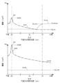
A-A線は、第1領域210および第1下面側領域230を通過するZ軸と平行な線であり、B-B線は、第2領域220および第2下面側領域240を通過するZ軸と平行な線である。図3の上段グラフはA-A線の各濃度分布を示し、下段グラフはB-B線の各濃度分布を示している。図3の各グラフにおける縦軸は各濃度(/cm3)を示す対数軸であり、横軸は下面23からの深さ位置(μm)を示す線形軸である。Line AA is a line parallel to the Z-axis passing through
A-A線におけるヘリウムの化学濃度をDheA、再結合中心の濃度をDrcA、水素の化学濃度をDhAとする。B-B線におけるヘリウムの化学濃度をDheB、再結合中心の濃度をDrcB、水素の化学濃度をDhBとする。本明細書における各化学濃度は、SIMSで計測してよい。 Let DheA be the chemical concentration of helium on the AA line, DrcA be the concentration of recombination centers, and DhA be the chemical concentration of hydrogen. Let DheB be the chemical concentration of helium on the BB line, DrcB be the concentration of recombination centers, and DhB be the chemical concentration of hydrogen. Each chemical concentration herein may be measured by SIMS.
第1領域210および第2領域220には、同一の工程でヘリウムが注入されるので、ヘリウム化学濃度DheAおよびヘリウム化学濃度DheBは、任意の深さ位置において同一であってよい。具体的には、第1領域210の第1深さ位置Z1におけるヘリウム化学濃度Dhe1Aと、第2領域220の第1深さ位置Z1におけるヘリウム化学濃度Dhe1Bは、同一の濃度であってよい。
Since the
ヘリウム化学濃度DheAの分布は、第1深さ位置Z1におけるピーク211と、ピーク211から上面21に向かう上側裾212と、ピーク211から下面23に向かう下側裾213を有する。本例のヘリウムは下面23から注入されている。この場合、上側裾212は、下側裾213よりもヘリウム化学濃度DheAが急峻に減少してよい。ピーク211におけるヘリウム化学濃度Dhe1Aは、第2深さ位置Z2におけるヘリウム化学濃度DheAの2倍以上であってよく、5倍以上であってよく、10倍以上であってもよい。
The distribution of the helium chemical concentration DheA has a peak 211 at the first depth position Z1, an
ヘリウム化学濃度DheBの分布は、第1深さ位置Z1におけるピーク221と、ピーク221から上面21に向かう上側裾222と、ピーク221から下面23に向かう下側裾223を有する。上側裾222は、下側裾223よりもヘリウム化学濃度DheBが急峻に減少してよい。
The distribution of the helium chemical concentration DheB has a peak 221 at the first depth position Z1, an
水素化学濃度DhAは、下面23から第1深さ位置Z1までの任意の深さ位置において、水素化学濃度DhBより小さい。A-A線における水素化学濃度DhAは、深さ方向においてほぼ一定であってよい。水素化学濃度DhAは0であってもよい。
The hydrogen chemical concentration DhA is smaller than the hydrogen chemical concentration DhB at any depth position from the
水素化学濃度DhBの分布は、第2深さ位置Z2にピーク241を有する。熱処理段階S203を行うことで、第2深さ位置Z2の近傍に注入された水素が、第1深さ位置Z1まで拡散する。水素化学濃度DhBは、第2深さ位置Z2から第1深さ位置Z1まで減少してよい。 The distribution of the hydrogen chemical concentration DhB has a peak 241 at the second depth position Z2. By performing the heat treatment step S203, the hydrogen implanted near the second depth position Z2 diffuses to the first depth position Z1. The hydrogen chemical concentration DhB may decrease from the second depth position Z2 to the first depth position Z1.
再結合中心濃度DrcAの分布は、ヘリウム化学濃度DheAの分布と相似形であってよい。相似形とは、分布におけるピークが、同一の深さ位置に配置されていることを指してよい。なお、一方のピークが、他方のピークの半値全幅の範囲内に配置されている場合、2つのピークが同一の深さ位置に配置されているとしてよい。本例の再結合中心濃度DrcAの分布は、第1領域210の第1深さ位置Z1にピーク251を有する。つまり第1領域210は、第1深さ位置Z1にキャリアライフタイムの極小値を有する。
The distribution of the recombination center concentration DrcA may be similar to the distribution of the helium chemical concentration DheA. Similarity may refer to peaks in the distribution being located at the same depth position. Note that when one peak is located within the full width at half maximum of the other peak, the two peaks may be located at the same depth position. The distribution of the recombination center concentration DrcA in this example has a peak 251 at the first depth position Z1 of the
再結合中心濃度DrcAの分布は、ピーク251から上面21に向かう上側裾252と、ピーク251から下面23に向かう下側裾253を有する。上側裾252は、下側裾253よりも再結合中心濃度DrcAが急峻に減少してよい。再結合中心濃度DrcAが、第1深さ位置Z1においてピーク251を有することで、第1深さ位置Z1の近傍におけるキャリアのライフタイムを短くできる。ピーク251における再結合中心濃度Drc1Aは、第2深さ位置Z2における再結合中心濃度Drc2Aの2倍以上であってよく、5倍以上であってよく、10倍以上であってもよい。
The distribution of the recombination center concentration DrcA has an
第2下面側領域240には水素イオンが注入されるので、再結合中心濃度DrcBは、再結合中心濃度DrcAに比べて小さくなる。再結合中心濃度DrcBは、下面23から第1深さ位置Z1までの任意の深さ位置において、再結合中心濃度DrcAより小さくてよい。再結合中心濃度DrcBの分布は、第1深さ位置Z1においてピークを有さなくてよい。第1深さ位置Z1における再結合中心濃度Drc1Bは、第2深さ位置Z2における再結合中心濃度DrcBと同一であってよく、1.5倍以下であってよく、2倍以下であってもよい。
Since hydrogen ions are implanted into the second lower
なお、再結合中心の濃度の大小は、キャリアのライフタイムを比較することで判別してよい。キャリアのライフタイムが短いほうを、再結合中心の濃度が高いとしてよい。本明細書で「再結合中心濃度がN倍」と規定した場合、「キャリアライフタイムが1/N倍」と読み替えてもよい。再結合中心の濃度の大小は、陽電子消滅法により空孔の濃度を測定し、その大小を比較することで判別してもよい。また、再結合中心の濃度の大小は、周知のデバイス・シミュレーションを用いて、後述するトランジスタ部またはダイオード部のオン電圧降下(順方向電圧降下)を算出し、当該特性の電気的測定値と比較することで判別してもよい。また、レーザー光照射とマイクロ波反射によりキャリアのライフタイムを測定してもよい。 The magnitude of the concentration of recombination centers may be determined by comparing carrier lifetimes. A carrier with a shorter lifetime may be considered to have a higher concentration of recombination centers. In the present specification, "the recombination center concentration is N times" may be read as "the carrier lifetime is 1/N times". The magnitude of the concentration of recombination centers may be determined by measuring the concentration of vacancies by the positron annihilation method and comparing the magnitudes. In addition, the magnitude of the concentration of the recombination center is determined by calculating the on-voltage drop (forward voltage drop) of the transistor section or diode section described later using well-known device simulation, and comparing it with the electrical measurement value of the characteristic. It can be determined by Alternatively, the carrier lifetime may be measured by laser light irradiation and microwave reflection.
図4は、A-A線における水素化学濃度DhAおよび再結合中心濃度DrcAと、B-B線における水素化学濃度DhBおよび再結合中心濃度DrcBを比較する図である。水素化学濃度DhA、再結合中心濃度DrcA、水素化学濃度DhBおよび再結合中心濃度DrcBの各分布は、図3に示した例と同一である。 FIG. 4 is a diagram comparing the hydrogen chemical concentration DhA and the recombination center concentration DrcA on the AA line with the hydrogen chemical concentration DhB and the recombination center concentration DrcB on the BB line. Each distribution of hydrogen chemical concentration DhA, recombination center concentration DrcA, hydrogen chemical concentration DhB and recombination center concentration DrcB is the same as the example shown in FIG.
上述したように、水素化学濃度DhBは、下面23から第1深さ位置Z1の全範囲に渡って、水素化学濃度DhAより大きくてよい。第2深さ位置Z2における水素化学濃度Dh2Bは、第2深さ位置Z2における水素化学濃度Dh2Aの10倍以上であってよく、100倍以上であってよく、1000倍以上であってよく、1010倍以上であってもよい。As described above, the hydrogen chemical concentration DhB may be greater than the hydrogen chemical concentration DhA over the entire range from the
第1深さ位置Z1における水素化学濃度Dh1Bは、第1深さ位置Z1における水素化学濃度Dh1Aの10倍以上であってよく、100倍以上であってよく、1000倍以上であってもよい。第2領域220の第1深さ位置Z1における水素化学濃度Dh1Bを高くすることで、第2領域220の第1深さ位置Z1における再結合中心濃度Drc1Bを小さくできる。第2領域220の第1深さ位置Z1における再結合中心濃度Drc1Bは、第1領域210の第1深さ位置Z1における再結合中心濃度Drc1Aの1/2以下であってよく、1/5以下であってよく、1/10以下であってよく、1/100以下であってもよい。
The hydrogen chemical concentration Dh1B at the first depth position Z1 may be 10 times or more, 100 times or more, or 1000 times or more the hydrogen chemical concentration Dh1A at the first depth position Z1. By increasing the hydrogen chemical concentration Dh1B at the first depth position Z1 of the
第1深さ位置Z1において、第1領域210のヘリウム化学濃度Dhe1A(図3参照)と、第2領域220のヘリウム化学濃度Dhe1B(図3参照)との比Dhe1A/Dhe1Bは、第1領域210の再結合中心の濃度Drc1Aと、第2領域220の再結合中心の濃度Drc1Bとの比Drc1A/Drc1Bよりも1に近い。Dhe1A/Dhe1Bは、1であってよい。つまり、第1領域210の再結合中心の濃度Drc1Aと、第2領域220の再結合中心の濃度Drc1Bは同じであってよい。Drc1A/Drc1Bは、2以上であってよく、5以上であってよく、10以上であってよく、100以上であってもよい。本例では、第1深さ位置Z1におけるヘリウム化学濃度が、第1領域210と第2領域220とでほぼ同一であるが、第1深さ位置Z1における再結合中心濃度は比較的に大きな差異を有する。
At the first depth position Z1, the ratio Dhe1A/Dhe1B between the helium chemical concentration Dhe1A in the first region 210 (see FIG. 3) and the helium chemical concentration Dhe1B in the second region 220 (see FIG. 3) is is closer to 1 than the ratio Drc1A/Drc1B between the concentration Drc1A of the recombination centers in the
第1領域210における再結合中心濃度DrcAのピーク251の半値全幅の深さ範囲をFWHM1とする。ピーク251の半値全幅の深さ範囲とは、ピーク251よりも上面21側において、再結合中心濃度DrcAがピーク濃度Drc1Aの半分になる位置から、ピーク251よりも下面23側において、再結合中心濃度DrcAがピーク濃度Drc1Aの半分になる位置までの範囲を指す。範囲FWHM1において、第1領域210における水素化学濃度DhAを深さ方向に積分した値を第1積分値とする。範囲FWHM1において、第2領域220における水素化学濃度DhBを深さ方向に積分した値を第2積分値とする。第1積分値は、第2積分値よりも小さい。第1積分値は、第2積分値の0.1倍以下であってよく、0.01倍以下であってよく、0.001倍以下であってもよい。
Let FWHM1 be the depth range of the full width at half maximum of the
第1領域210における第1深さ位置Z1から下面23までの範囲で水素化学濃度DhAを深さ方向に積分した値を第3積分値とする。第2領域220における第1深さ位置Z1から下面23までの範囲で水素化学濃度DhBを深さ方向に積分した値を第4積分値とする。第3積分値は、第4積分値よりも小さい。第3積分値は、第4積分値の0.1倍以下であってよく、0.01倍以下であってよく、0.001倍以下であってもよい。
A value obtained by integrating the hydrogen chemical concentration DhA in the depth direction in the range from the first depth position Z1 to the
なお、半導体基板10において荷電粒子が通過した通過領域には、水素が通過したことにより、単原子空孔(V)、複原子空孔(VV)等の、空孔を主体とする格子欠陥(再結合中心)が形成されている。空孔に隣接する原子は、ダングリング・ボンドを有する。格子欠陥には格子間原子や転位等も含まれ、広義ではドナーやアクセプタも含まれ得るが、本明細書では空孔を主体とする格子欠陥を空孔型格子欠陥、空孔型欠陥、あるいは単に格子欠陥と称する場合がある。また、半導体基板10への荷電粒子注入により、格子欠陥が多く形成されることで、半導体基板10の結晶性が強く乱れることがある。本明細書では、この結晶性の乱れをディスオーダーと称する場合がある。
In the
また、半導体基板10の全体には酸素が含まれる。当該酸素は、半導体のインゴットの製造時において、意図的にまたは意図せずに導入される。半導体基板10の内部では、水素(H)、空孔(V)および酸素(O)が結合し、VOH欠陥が形成される。また、半導体基板10を熱処理することで水素が拡散し、VOH欠陥の形成が促進される。VOH欠陥は、電子を供給するドナーとして機能する。本明細書では、VOH欠陥を単に水素ドナーと称する場合がある。
In addition, the
本例の半導体基板10には、第2領域220と第2下面側領域240との間の第2通過領域に水素ドナーが形成される。一方で、第1領域210と第1下面側領域230との間の第1通過領域には水素ドナーが形成されにくい。第2通過領域におけるドーピング濃度は、第1通過領域におけるドーピング濃度より高くてよい。第2通過領域におけるドーピング濃度を深さ方向に積分した積分値が、第1通過領域におけるドーピング濃度を深さ方向に積分した積分値よりも大きくてよい。
In the
図5は、図1および図2のA-A線およびB-B線における、荷電粒子、再結合中心および水素の濃度分布の他の例を示している。本例の荷電粒子は水素(注入時は水素イオン)である。図5の各濃度は、熱処理段階S203の後の分布である。荷電粒子以外の条件は、図3の例と同一である。荷電粒子の種類以外は、特に説明する場合を除き、図3および図4に示した例と同様の構造(各濃度分布を含む)であってよい。 FIG. 5 shows another example of concentration distributions of charged particles, recombination centers and hydrogen along lines AA and BB of FIGS. 1 and 2. FIG. The charged particles in this example are hydrogen (hydrogen ions when implanted). Each concentration in FIG. 5 is the distribution after the heat treatment step S203. Conditions other than charged particles are the same as in the example of FIG. Other than the type of charged particles, the structure (including each concentration distribution) may be the same as the examples shown in FIGS. 3 and 4, unless otherwise specified.
A-A線における水素の化学濃度をDhA1、再結合中心の濃度をDrcAとする。B-B線において、第1深さ位置Z1に注入された水素の化学濃度をDhB1、第2深さ位置に注入された水素の化学濃度をDhB2、再結合中心の濃度をDrcBとする。本例では、水素化学濃度DhB1およびDhB2を加算した水素化学濃度をDhBと称する。 Let DhA1 be the chemical concentration of hydrogen on line AA, and DrcA be the concentration of recombination centers. On line BB, the chemical concentration of hydrogen implanted at the first depth position Z1 is DhB1, the chemical concentration of hydrogen implanted at the second depth position is DhB2, and the concentration at the recombination center is DrcB. In this example, the sum of the hydrogen chemical concentrations DhB1 and DhB2 is referred to as DhB.
図3に示したヘリウム化学濃度と同様に、水素化学濃度DhA1の分布は第1深さ位置Z1にピーク211を有してよい。水素化学濃度DhA1の分布は、上側裾212および下側裾213を有してよい。水素化学濃度DhBの分布は第1深さ位置Z1にピーク221を有してよい。水素化学濃度DhBの分布は、上側裾222および下側裾223を有してよい。
Similar to the helium chemical concentration shown in FIG. 3, the distribution of hydrogen chemical concentration DhA1 may have a peak 211 at the first depth location Z1. The distribution of hydrogen chemical concentration DhA1 may have an
再結合中心濃度DrcAは、第1深さ位置Z1の近傍においてピーク251を有してよい。本例では荷電粒子が水素なので、第1深さ位置Z1に多くの水素が存在する。つまり、第1深さ位置Z1の再結合中心は水素で終端されやすい。ピーク251は、第1深さ位置Z1よりも下面23側に配置されていてもよい。再結合中心濃度DrcBは、図3および図4に示した例と同様である。ピーク241における水素化学濃度Dh2Bは、ピーク221における水素化学濃度Dh1Bの10倍以上であってよく、100倍以上であってよく、1000倍以上であってもよい。図5において説明したように、荷電粒子として水素イオンを用いた場合においても、再結合中心を局所的に設けることができる。
The recombination center concentration DrcA may have a
図6は、半導体装置100の製造方法の他の例を説明する図である。本例の製造方法は、図2において説明した熱処理段階S203の後に、研削段階S204を更に備える。研削段階S204では、第2注入段階S202で水素イオンを注入することで形成された水素化学濃度のピーク(例えば、図3から図5において説明したピーク241)を含む半導体基板10の部分を、下面23側から研削する。つまり、研削段階S204では、第2深さ位置Z2を超える深さ位置まで、下面23を研削する。研削した後の半導体基板10は、下面123を有する。下面123の深さ位置は、第2深さ位置Z2よりも上面21側に配置されている。
6A and 6B are diagrams for explaining another example of the method for manufacturing the
本例によれば、水素化学濃度のピーク241を削除できる。ピーク241の近傍においては、VOH欠陥が比較的に多く形成されるので、ドーピング濃度が高くなる。本例によれば、ドーピング濃度が高くなった領域を研削するので、ピーク241を設けたことによる半導体装置100の特性への影響を抑制できる。
According to this example, the hydrogen
図7は、半導体装置100の製造方法の他の例を説明する図である。本例における荷電粒子は電子である。荷電粒子の種類以外の製造条件、製造工程および装置の構造は、図1から図6において説明したいずれかの例と同様である。
7A and 7B are diagrams for explaining another example of the method for manufacturing the
本例においては、第1注入段階S701において、半導体基板10の下面23から電子線を照射する。半導体基板10に注入された電子は、半導体基板10を貫通して、上面21から外部に放出されてよい。電子が通過した領域には、深さ方向においてほぼ均一濃度の再結合中心が形成されてよい。
In this example, an electron beam is irradiated from the
次に第2注入段階S702において、第2深さ位置Z2に水素イオンを注入する。図2に示した例と同様に、第2注入段階S702においては、第2下面側領域240だけに水素イオンを注入してよい。他の例では、第1下面側領域230および第2下面側領域240の両方に水素イオンを注入してもよい。ただし、第1下面側領域230への水素イオンのドーズ量は、第2下面側領域240への水素イオンのドーズ量よりも少ない。
Next, in a second implantation step S702, hydrogen ions are implanted at the second depth Z2. Similar to the example shown in FIG. 2, hydrogen ions may be implanted only into the second
次に熱処理段階S703において、半導体基板10を熱処理する。熱処理段階S703では、第2下面側領域240に注入した水素が第2領域220の第1深さ位置Z1まで拡散する条件で熱処理する。第1下面側領域230の水素化学濃度は、第2下面側領域240の水素化学濃度よりも低いので、第1領域210まで拡散する水素化学濃度は、第2領域220まで拡散する水素化学濃度よりも低い。このため、第1領域210における再結合中心の濃度を、第2領域220における再結合中心の濃度よりも高くできる。熱処理段階S703では、第1下面側領域230に注入した水素が第1領域210の第1深さ位置Z1まで拡散しない条件で熱処理してよい。
Next, in a heat treatment step S703, the
図8は、図7のA-A線およびB-B線における、再結合中心および水素の濃度分布を示している。図8の各濃度は、熱処理段階S703の後の分布である。荷電粒子以外の条件は、図3の例と同一である。荷電粒子の種類以外は、特に説明する場合を除き、図3および図4に示した例と同様の構造(各濃度分布を含む)であってよい。 FIG. 8 shows the concentration distribution of recombination centers and hydrogen along lines AA and BB of FIG. Each concentration in FIG. 8 is the distribution after the heat treatment step S703. Conditions other than charged particles are the same as in the example of FIG. Other than the type of charged particles, the structure (including each concentration distribution) may be the same as the examples shown in FIGS. 3 and 4, unless otherwise specified.
本例においては、第1下面側領域230にも水素イオンが注入されている。A-A線における水素化学濃度DhAは、第2深さ位置Z2にピーク231を有する。ただし、ピーク231における水素化学濃度Dh2Aは、ピーク241における水素化学濃度Dh2Bよりも低い。水素化学濃度Dh2Aは、水素化学濃度Dh2Bの1/2以下であってよく、1/10以下であってよく、1/100以下であってもよい。
In this example, hydrogen ions are also implanted into the first lower
第1深さ位置Z1において、A-A線の水素化学濃度Dh1Aは、B-B線の水素化学濃度Dh1Bよりも低い。水素化学濃度Dh1Aは、水素化学濃度Dh1Bの1/2以下であってよく、1/10以下であってよく、1/100以下であってもよい。水素化学濃度Dh1Aはほぼ0であってもよい。 At the first depth position Z1, the hydrogen chemical concentration Dh1A on the AA line is lower than the hydrogen chemical concentration Dh1B on the BB line. The hydrogen chemical concentration Dh1A may be 1/2 or less, 1/10 or less, or 1/100 or less of the hydrogen chemical concentration Dh1B. The hydrogen chemical concentration Dh1A may be approximately zero.
本例の再結合中心濃度DrcAの分布は、第1深さ位置Z1にピークを有さなくてもよい。再結合中心濃度DrcAの分布は、水素化学濃度DhAがほぼ0となる深さ位置から、上面21に向かって徐々に増大してよい。第1深さ位置Z1は、再結合中心濃度Drc1Aが、再結合中心濃度DrcAの最大値DrcAmaxの半値となる位置であってよい。再結合中心濃度DrcAの最大値DrcAmaxは、後述するドリフト領域18における最大値であってよい。第1深さ位置Z1において、再結合中心濃度Drc1Aは、再結合中心濃度Drc1Bの2倍以上であってよく、5倍以上であってよく、10倍以上であってもよい。
The distribution of the recombination center concentration DrcA in this example may not have a peak at the first depth position Z1. The distribution of the recombination center concentration DrcA may gradually increase toward the
なお、図8以外の例においても、第1下面側領域230に水素イオンを注入してよい。ただし。第1下面側領域230の水素イオンの単位面積当たりのドーズ量は、第2下面側領域240の水素イオンの単位面積当たりのドーズ量よりも少ない。
Note that hydrogen ions may be implanted into the first lower
図9は、半導体装置100の他の構造例を示す図である。本例の半導体装置100は、第1下面側領域230および第2下面側領域240に代えて、第1上面側領域260および第2上面側領域270を備える。他の構造は、図1から図8において説明したいずれかの例と同様である。
FIG. 9 is a diagram showing another structural example of the
第1上面側領域260は、第1領域210と上面21との間に配置されている。第2上面側領域270は、第2領域220と上面21との間に配置されている。本例では、上面21から、第2上面側領域270の第3深さ位置Z3に水素イオンを注入する。第3深さ位置Z3は、第1深さ位置Z1よりも上面21側に位置してよい。第1上面側領域260には、水素イオンを注入してよく、しなくてもよい。ただし、第1上面側領域260への水素イオンのドーズ量は、第2上面側領域270への水素イオンのドーズ量よりも少ない。本例においても、第2上面側領域270に注入した水素が、第2領域220に拡散することで、第2領域220における再結合中心の濃度を低くできる。
The first upper
図10は、図9に示した半導体装置100の製造方法の一例を示す図である。まず第1注入段階S1001において、下面23から荷電粒子を注入する。本例の荷電粒子は、水素イオンまたはヘリウムイオン等のイオンである。第1注入段階S1001は、図2等において説明した第1注入段階S201と同様である。
10A and 10B are diagrams showing an example of a method for manufacturing the
次に、第2注入段階S1002において、上面21から第3深さ位置Z3に水素イオンを注入する。第3深さ位置Z3と上面21との距離は、第1深さ位置Z1と上面21との距離の半分以下であってよく、1/4以下であってよく、1/10以下であってよく、1/20以下であってもよい。本例では、第2上面側領域270に水素イオンを注入する。第1上面側領域260には、水素イオンを注入しないか、または、第2上面側領域270よりも少ないドーズ量で水素イオンを注入する。
Next, in a second implantation step S1002, hydrogen ions are implanted from the
第2上面側領域270は、第2領域220とXY面において同一の位置に設けられてよい。第1上面側領域260は、第1領域210とXY面において同一の位置に設けられてよい。第1上面側領域260および第2上面側領域270は、XY面において接して配置されていてよい。また、第1上面側領域260および第2上面側領域270は、共に第3深さ位置Z3を含む深さ範囲に設けられている。なお、第2注入段階S1002においては、半導体基板10の上面21に、第1上面側領域260を覆うフォトレジスト等のマスクを形成することで、第1上面側領域260への水素イオンを遮蔽してよい。
The second upper
次に、熱処理段階S1003において、半導体基板10を熱処理する。熱処理段階S1003では、第2上面側領域270の第3深さ位置Z3に注入された水素が、第2領域220の第1深さ位置Z1まで拡散する条件で、半導体基板10を熱処理する。これにより、第2領域220の再結合中心の濃度が低下する。従って、第1領域210の再結合中心を選択的に残存させることができる。このため、半導体装置100の特性を容易に調整できる。
Next, in a heat treatment step S1003, the
なお、本例においては水素イオンを上面21から注入している。ただし、水素イオンの飛程は、荷電粒子の飛程よりも短い。このため、水素イオンの注入による半導体基板10へのダメージは比較的に小さい。本例によっても、半導体基板10へのダメージを抑制しつつ、再結合中心を選択的に設けることができる。
Note that hydrogen ions are implanted from the
図11は、図10のA-A線およびB-B線における、荷電粒子、再結合中心および水素の濃度分布を示している。本例の荷電粒子はヘリウム(注入時はヘリウムイオン)である。図11の各濃度は、熱処理段階S1003の後の分布である。本例においては、B-B線における水素化学濃度DhBの分布が、図3に示した水素化学濃度DhBの分布と異なる。他の濃度分布は、図3に示した例と同様である。 FIG. 11 shows the concentration distributions of charged particles, recombination centers and hydrogen along lines AA and BB of FIG. The charged particles in this example are helium (helium ions when implanted). Each concentration in FIG. 11 is the distribution after the heat treatment step S1003. In this example, the distribution of the hydrogen chemical concentration DhB on the BB line differs from the distribution of the hydrogen chemical concentration DhB shown in FIG. Other density distributions are similar to the example shown in FIG.
水素化学濃度DhBの分布は、第3深さ位置Z3にピーク241を有する。熱処理段階S1003を行うことで、第3深さ位置Z3の近傍に注入された水素が、第1深さ位置Z1まで拡散する。水素化学濃度DhBは、第3深さ位置Z3から第1深さ位置Z1まで減少してよい。 The distribution of the hydrogen chemical concentration DhB has a peak 241 at the third depth position Z3. By performing the heat treatment step S1003, the hydrogen implanted near the third depth position Z3 diffuses to the first depth position Z1. The hydrogen chemical concentration DhB may decrease from the third depth position Z3 to the first depth position Z1.
水素化学濃度DhBは、上面21から第1深さ位置Z1の全範囲に渡って、水素化学濃度DhAより大きくてよい。第3深さ位置Z3における水素化学濃度Dh3Bは、第3深さ位置Z3における水素化学濃度DhAの10倍以上であってよく、100倍以上であってよく、1000倍以上であってよく、1010倍以上であってもよい。The hydrogen chemical concentration DhB may be greater than the hydrogen chemical concentration DhA over the entire range from the
第1深さ位置Z1における水素化学濃度Dh1Bは、第1深さ位置Z1における水素化学濃度DhAの10倍以上であってよく、100倍以上であってよく、1000倍以上であってもよい。第2領域220の第1深さ位置Z1における再結合中心濃度Drc1Bは、第1領域210の第1深さ位置Z1における再結合中心濃度Drc1Aの1/2以下であってよく、1/5以下であってよく、1/10以下であってよく、1/100以下であってもよい。
The hydrogen chemical concentration Dh1B at the first depth position Z1 may be 10 times or more, 100 times or more, or 1000 times or more the hydrogen chemical concentration DhA at the first depth position Z1. The recombination center concentration Drc1B at the first depth position Z1 of the
第1領域210における再結合中心濃度DrcAのピーク251の半値全幅の深さ範囲をFWHM1とする。範囲FWHM1において、第1領域210における水素化学濃度DhAを深さ方向に積分した値を第5積分値とする。範囲FWHM1において、第2領域220における水素化学濃度DhBを深さ方向に積分した値を第6積分値とする。第5積分値は、第6積分値よりも小さい。第5積分値は、第6積分値の0.1倍以下であってよく、0.01倍以下であってよく、0.001倍以下であってもよい。
Let FWHM1 be the depth range of the full width at half maximum of the
第1領域210における第1深さ位置Z1から上面21までの範囲で水素化学濃度DhAを深さ方向に積分した値を第7積分値とする。第2領域220における第1深さ位置Z1から上面21までの範囲で水素化学濃度DhBを深さ方向に積分した値を第8積分値とする。第7積分値は、第8積分値よりも小さい。第7積分値は、第8積分値の0.1倍以下であってよく、0.01倍以下であってよく、0.001倍以下であってもよい。
A value obtained by integrating the hydrogen chemical concentration DhA in the depth direction in the range from the first depth position Z1 to the
図12は、半導体装置100の一例を示す上面図である。図12においては、各部材を半導体基板10の上面に投影した位置を示している。図12においては、半導体装置100の一部の部材だけを示しており、一部の部材は省略している。
FIG. 12 is a top view showing an example of the
半導体装置100は、半導体基板10を備えている。半導体基板10は、図1から図11において説明した水素化学濃度分布、荷電粒子濃度分布および再結合中心濃度分布を有してよい。ただし半導体基板10は、図1から図11において説明した各濃度ピークとは異なる他の濃度ピークを更に有していてよい。後述するバッファ領域20のように、水素イオンを注入して半導体基板10におけるN型領域を形成する場合がある。この場合、水素化学濃度分布は、図1から図11において説明した水素化学濃度の分布の他に、局所的な水素濃度ピークを有し得る。また、後述するエミッタ領域12等のように、所定のドーパントを局所的に注入して、所定の導電型の領域を形成する場合がある。この場合、再結合中心の濃度分布は、ドーパントの飛程近傍に局所的なピークを有し得る。
A
半導体基板10は、上面視において端辺162を有する。本明細書で単に上面視と称した場合、半導体基板10の上面側から見ることを意味している。本例の半導体基板10は、上面視において互いに向かい合う2組の端辺162を有する。図12においては、X軸およびY軸は、いずれかの端辺162と平行である。またZ軸は、半導体基板10の上面と垂直である。
The
半導体基板10には活性部160が設けられている。活性部160は、半導体装置100が動作した場合に半導体基板10の上面と下面との間で、深さ方向に主電流が流れる領域である。活性部160の上方には、エミッタ電極が設けられているが図12では省略している。
An
活性部160には、IGBT等のトランジスタ素子を含むトランジスタ部70と、還流ダイオード(FWD)等のダイオード素子を含むダイオード部80の少なくとも一方が設けられている。図12の例では、トランジスタ部70およびダイオード部80は、半導体基板10の上面における所定の配列方向(本例ではX軸方向)に沿って、交互に配置されている。他の例では、活性部160には、トランジスタ部70およびダイオード部80の一方だけが設けられていてもよい。
At least one of a
図12においては、トランジスタ部70が配置される領域には記号「I」を付し、ダイオード部80が配置される領域には記号「F」を付している。本明細書では、上面視において配列方向と垂直な方向を延伸方向(図12ではY軸方向)と称する場合がある。トランジスタ部70およびダイオード部80は、それぞれ延伸方向に長手を有してよい。つまり、トランジスタ部70のY軸方向における長さは、X軸方向における幅よりも大きい。同様に、ダイオード部80のY軸方向における長さは、X軸方向における幅よりも大きい。トランジスタ部70およびダイオード部80の延伸方向と、後述する各トレンチ部の長手方向とは同一であってよい。
In FIG. 12, the region where the
ダイオード部80は、半導体基板10の下面と接する領域に、N+型のカソード領域を有する。本明細書では、カソード領域が設けられた領域を、ダイオード部80と称する。つまりダイオード部80は、上面視においてカソード領域と重なる領域である。半導体基板10の下面には、カソード領域以外の領域には、P+型のコレクタ領域が設けられてよい。本明細書では、ダイオード部80を、後述するゲート配線までY軸方向に延長した延長領域81も、ダイオード部80に含める場合がある。延長領域81の下面には、コレクタ領域が設けられている。
The
トランジスタ部70は、半導体基板10の下面と接する領域に、P+型のコレクタ領域を有する。また、トランジスタ部70は、半導体基板10の上面側に、N型のエミッタ領域、P型のベース領域、ゲート導電部およびゲート絶縁膜を有するゲート構造が周期的に配置されている。
The
半導体装置100は、半導体基板10の上方に1つ以上のパッドを有してよい。本例の半導体装置100は、ゲートパッド164を有している。半導体装置100は、アノードパッド、カソードパッドおよび電流検出パッド等のパッドを有してもよい。各パッドは、端辺162の近傍に配置されている。端辺162の近傍とは、上面視における端辺162と、エミッタ電極との間の領域を指す。半導体装置100の実装時において、各パッドは、ワイヤ等の配線を介して外部の回路に接続されてよい。
ゲートパッド164には、ゲート電位が印加される。ゲートパッド164は、活性部160のゲートトレンチ部の導電部に電気的に接続される。半導体装置100は、ゲートパッド164とゲートトレンチ部とを接続するゲート配線を備える。図12においては、ゲート配線に斜線のハッチングを付している。
A gate potential is applied to the
本例のゲート配線は、外周ゲート配線130と、活性側ゲート配線131とを有している。外周ゲート配線130は、上面視において活性部160と半導体基板10の端辺162との間に配置されている。本例の外周ゲート配線130は、上面視において活性部160を囲んでいる。上面視において外周ゲート配線130に囲まれた領域を活性部160としてもよい。また、外周ゲート配線130は、ゲートパッド164と接続されている。外周ゲート配線130は、半導体基板10の上方に配置されている。外周ゲート配線130は、アルミニウム等を含む金属配線であってよい。
The gate wiring of this example has a
活性側ゲート配線131は、活性部160に設けられている。活性部160に活性側ゲート配線131を設けることで、半導体基板10の各領域について、ゲートパッド164からの配線長のバラツキを低減できる。
The active-
活性側ゲート配線131は、活性部160のゲートトレンチ部と接続される。活性側ゲート配線131は、半導体基板10の上方に配置されている。活性側ゲート配線131は、不純物がドープされたポリシリコン等の半導体で形成された配線であってよい。
The active-
活性側ゲート配線131は、外周ゲート配線130と接続されてよい。本例の活性側ゲート配線131は、Y軸方向の略中央で一方の外周ゲート配線130から他方の外周ゲート配線130まで、活性部160を横切るように、X軸方向に延伸して設けられている。活性側ゲート配線131により活性部160が分割されている場合、それぞれの分割領域において、トランジスタ部70およびダイオード部80がX軸方向に交互に配置されてよい。
The active
また、半導体装置100は、ポリシリコン等で形成されたPN接合ダイオードである不図示の温度センス部や、活性部160に設けられたトランジスタ部の動作を模擬する不図示の電流検出部を備えてもよい。
The
本例の半導体装置100は、上面視において、活性部160と端辺162との間に、エッジ終端構造部90を備える。本例のエッジ終端構造部90は、外周ゲート配線130と端辺162との間に配置されている。エッジ終端構造部90は、半導体基板10の上面側の電界集中を緩和する。エッジ終端構造部90は、活性部160を囲んで環状に設けられたガードリング、フィールドプレートおよびリサーフのうちの少なくとも一つを備えていてよい。
The
図13は、図12における領域Dの拡大図である。領域Dは、トランジスタ部70、ダイオード部80、および、活性側ゲート配線131を含む領域である。本例の半導体装置100は、半導体基板10の上面側の内部に設けられたゲートトレンチ部40、ダミートレンチ部30、ウェル領域11、エミッタ領域12、ベース領域14およびコンタクト領域15を備える。ゲートトレンチ部40およびダミートレンチ部30は、それぞれがトレンチ部の一例である。また、本例の半導体装置100は、半導体基板10の上面の上方に設けられたエミッタ電極52および活性側ゲート配線131を備える。エミッタ電極52および活性側ゲート配線131は互いに分離して設けられる。
13 is an enlarged view of region D in FIG. 12. FIG. Region D is a region including
エミッタ電極52および活性側ゲート配線131と、半導体基板10の上面との間には層間絶縁膜が設けられるが、図13では省略している。本例の層間絶縁膜には、コンタクトホール54が、当該層間絶縁膜を貫通して設けられる。図13においては、それぞれのコンタクトホール54に斜線のハッチングを付している。
An interlayer insulating film is provided between the
エミッタ電極52は、ゲートトレンチ部40、ダミートレンチ部30、ウェル領域11、エミッタ領域12、ベース領域14およびコンタクト領域15の上方に設けられる。エミッタ電極52は、コンタクトホール54を通って、半導体基板10の上面におけるエミッタ領域12、コンタクト領域15およびベース領域14と接触する。また、エミッタ電極52は、層間絶縁膜に設けられたコンタクトホールを通って、ダミートレンチ部30内のダミー導電部と接続される。エミッタ電極52は、Y軸方向におけるダミートレンチ部30の先端において、ダミートレンチ部30のダミー導電部と接続されてよい。
活性側ゲート配線131は、層間絶縁膜に設けられたコンタクトホールを通って、ゲートトレンチ部40と接続する。活性側ゲート配線131は、Y軸方向におけるゲートトレンチ部40の先端部41において、ゲートトレンチ部40のゲート導電部と接続されてよい。活性側ゲート配線131は、ダミートレンチ部30内のダミー導電部とは接続されない。
The active-
エミッタ電極52は、金属を含む材料で形成される。図13においては、エミッタ電極52が設けられる範囲を示している。例えば、エミッタ電極52の少なくとも一部の領域はアルミニウムまたはアルミニウム‐シリコン合金、例えばAlSi、AlSiCu等の金属合金で形成される。エミッタ電極52は、アルミニウム等で形成された領域の下層に、チタンやチタン化合物等で形成されたバリアメタルを有してよい。さらにコンタクトホール内において、バリアメタルとアルミニウム等に接するようにタングステン等を埋め込んで形成されたプラグを有してもよい。
The
ウェル領域11は、活性側ゲート配線131と重なって設けられている。ウェル領域11は、活性側ゲート配線131と重ならない範囲にも、所定の幅で延伸して設けられている。本例のウェル領域11は、コンタクトホール54のY軸方向の端から、活性側ゲート配線131側に離れて設けられている。ウェル領域11は、ベース領域14よりもドーピング濃度の高い第2導電型の領域である。本例のベース領域14はP-型であり、ウェル領域11はP+型である。
The
トランジスタ部70およびダイオード部80のそれぞれは、配列方向に複数配列されたトレンチ部を有する。本例のトランジスタ部70には、配列方向に沿って1以上のゲートトレンチ部40と、1以上のダミートレンチ部30とが交互に設けられている。本例のダイオード部80には、複数のダミートレンチ部30が、配列方向に沿って設けられている。本例のダイオード部80には、ゲートトレンチ部40が設けられていない。
Each of the
本例のゲートトレンチ部40は、配列方向と垂直な延伸方向に沿って延伸する2つの直線部分39(延伸方向に沿って直線状であるトレンチの部分)と、2つの直線部分39を接続する先端部41を有してよい。図13における延伸方向はY軸方向である。
The
先端部41の少なくとも一部は、上面視において曲線状に設けられることが好ましい。2つの直線部分39のY軸方向における端部どうしを先端部41が接続することで、直線部分39の端部における電界集中を緩和できる。
It is preferable that at least part of the
トランジスタ部70において、ダミートレンチ部30はゲートトレンチ部40のそれぞれの直線部分39の間に設けられる。それぞれの直線部分39の間には、1本のダミートレンチ部30が設けられてよく、複数本のダミートレンチ部30が設けられていてもよい。ダミートレンチ部30は、延伸方向に延伸する直線形状を有してよく、ゲートトレンチ部40と同様に、直線部分29と先端部31とを有していてもよい。図13に示した半導体装置100は、先端部31を有さない直線形状のダミートレンチ部30と、先端部31を有するダミートレンチ部30の両方を含んでいる。
In the
ウェル領域11の拡散深さは、ゲートトレンチ部40およびダミートレンチ部30の深さよりも深くてよい。ゲートトレンチ部40およびダミートレンチ部30のY軸方向の端部は、上面視においてウェル領域11に設けられる。つまり、各トレンチ部のY軸方向の端部において、各トレンチ部の深さ方向の底部は、ウェル領域11に覆われている。これにより、各トレンチ部の当該底部における電界集中を緩和できる。
The diffusion depth of
配列方向において各トレンチ部の間には、メサ部が設けられている。メサ部は、半導体基板10の内部において、トレンチ部に挟まれた領域を指す。一例としてメサ部の上端は半導体基板10の上面である。メサ部の下端の深さ位置は、トレンチ部の下端の深さ位置と同一である。本例のメサ部は、半導体基板10の上面において、トレンチに沿って延伸方向(Y軸方向)に延伸して設けられている。本例では、トランジスタ部70にはメサ部60が設けられ、ダイオード部80にはメサ部61が設けられている。本明細書において単にメサ部と称した場合、メサ部60およびメサ部61のそれぞれを指している。
A mesa portion is provided between each trench portion in the arrangement direction. The mesa portion refers to a region sandwiched between trench portions inside the
それぞれのメサ部には、ベース領域14が設けられる。メサ部において半導体基板10の上面に露出したベース領域14のうち、活性側ゲート配線131に最も近く配置された領域をベース領域14-eとする。図13においては、それぞれのメサ部の延伸方向における一方の端部に配置されたベース領域14-eを示しているが、それぞれのメサ部の他方の端部にもベース領域14-eが配置されている。それぞれのメサ部には、上面視においてベース領域14-eに挟まれた領域に、第1導電型のエミッタ領域12および第2導電型のコンタクト領域15の少なくとも一方が設けられてよい。本例のエミッタ領域12はN+型であり、コンタクト領域15はP+型である。エミッタ領域12およびコンタクト領域15は、深さ方向において、ベース領域14と半導体基板10の上面との間に設けられてよい。
Each mesa is provided with a
トランジスタ部70のメサ部60は、半導体基板10の上面に露出したエミッタ領域12を有する。エミッタ領域12は、ゲートトレンチ部40に接して設けられている。ゲートトレンチ部40に接するメサ部60は、半導体基板10の上面に露出したコンタクト領域15が設けられていてよい。
The
メサ部60におけるコンタクト領域15およびエミッタ領域12のそれぞれは、X軸方向における一方のトレンチ部から、他方のトレンチ部まで設けられる。一例として、メサ部60のコンタクト領域15およびエミッタ領域12は、トレンチ部の延伸方向(Y軸方向)に沿って交互に配置されている。
Each of the
他の例においては、メサ部60のコンタクト領域15およびエミッタ領域12は、トレンチ部の延伸方向(Y軸方向)に沿ってストライプ状に設けられていてもよい。例えばトレンチ部に接する領域にエミッタ領域12が設けられ、エミッタ領域12に挟まれた領域にコンタクト領域15が設けられる。
In another example, the
ダイオード部80のメサ部61には、エミッタ領域12が設けられていない。メサ部61の上面には、ベース領域14およびコンタクト領域15が設けられてよい。メサ部61の上面においてベース領域14-eに挟まれた領域には、それぞれのベース領域14-eに接してコンタクト領域15が設けられてよい。メサ部61の上面においてコンタクト領域15に挟まれた領域には、ベース領域14が設けられてよい。ベース領域14は、コンタクト領域15に挟まれた領域全体に配置されてよい。
The
それぞれのメサ部の上方には、コンタクトホール54が設けられている。コンタクトホール54は、ベース領域14-eに挟まれた領域に配置されている。本例のコンタクトホール54は、コンタクト領域15、ベース領域14およびエミッタ領域12の各領域の上方に設けられる。コンタクトホール54は、ベース領域14-eおよびウェル領域11に対応する領域には設けられない。コンタクトホール54は、メサ部60の配列方向(X軸方向)における中央に配置されてよい。
A
ダイオード部80において、半導体基板10の下面と隣接する領域には、N+型のカソード領域82が設けられる。半導体基板10の下面において、カソード領域82が設けられていない領域には、P+型のコレクタ領域22が設けられてよい。カソード領域82およびコレクタ領域22は、半導体基板10の下面23と、バッファ領域20との間に設けられている。図13においては、カソード領域82およびコレクタ領域22の境界を点線で示している。
In the
カソード領域82は、Y軸方向においてウェル領域11から離れて配置されている。これにより、比較的にドーピング濃度が高く、且つ、深い位置まで形成されているP型の領域(ウェル領域11)と、カソード領域82との距離を確保して、耐圧を向上できる。本例のカソード領域82のY軸方向における端部は、コンタクトホール54のY軸方向における端部よりも、ウェル領域11から離れて配置されている。他の例では、カソード領域82のY軸方向における端部は、ウェル領域11とコンタクトホール54との間に配置されていてもよい。
The
図14は、図13におけるe-e断面の一例を示す図である。e-e断面は、エミッタ領域12およびカソード領域82を通過するXZ面である。本例の半導体装置100は、当該断面において、半導体基板10、層間絶縁膜38、エミッタ電極52およびコレクタ電極24を有する。
FIG. 14 is a diagram showing an example of the ee cross section in FIG. The ee section is the XZ plane passing through
層間絶縁膜38は、半導体基板10の上面に設けられている。層間絶縁膜38は、ホウ素またはリン等の不純物が添加されたシリケートガラス等の絶縁膜、熱酸化膜、および、その他の絶縁膜の少なくとも一層を含む膜である。層間絶縁膜38には、図13において説明したコンタクトホール54が設けられている。
An interlayer insulating
エミッタ電極52は、層間絶縁膜38の上方に設けられる。エミッタ電極52は、層間絶縁膜38のコンタクトホール54を通って、半導体基板10の上面21と接触している。コレクタ電極24は、半導体基板10の下面23に設けられる。エミッタ電極52およびコレクタ電極24は、アルミニウム等の金属材料で形成されている。本明細書において、エミッタ電極52とコレクタ電極24とを結ぶ方向(Z軸方向)を深さ方向と称する。
半導体基板10は、N型またはN-型のドリフト領域18を有する。ドリフト領域18は、トランジスタ部70およびダイオード部80のそれぞれに設けられている。
トランジスタ部70のメサ部60には、N+型のエミッタ領域12およびP-型のベース領域14が、半導体基板10の上面21側から順番に設けられている。ベース領域14の下方にはドリフト領域18が設けられている。メサ部60には、N+型の蓄積領域16が設けられてもよい。蓄積領域16は、ベース領域14とドリフト領域18との間に配置される。
In the
エミッタ領域12は半導体基板10の上面21に露出しており、且つ、ゲートトレンチ部40と接して設けられている。エミッタ領域12は、メサ部60の両側のトレンチ部と接していてよい。エミッタ領域12は、ドリフト領域18よりもドーピング濃度が高い。
The
ベース領域14は、エミッタ領域12の下方に設けられている。本例のベース領域14は、エミッタ領域12と接して設けられている。ベース領域14は、メサ部60の両側のトレンチ部と接していてよい。
A
蓄積領域16は、ベース領域14の下方に設けられている。蓄積領域16は、ドリフト領域18よりもドーピング濃度が高いN+型の領域である。ドリフト領域18とベース領域14との間に高濃度の蓄積領域16を設けることで、キャリア注入促進効果(IE効果)を高めて、オン電圧を低減できる。蓄積領域16は、各メサ部60におけるベース領域14の下面全体を覆うように設けられてよい。
An
ダイオード部80のメサ部61には、半導体基板10の上面21に接して、P-型のベース領域14が設けられている。ベース領域14の下方には、ドリフト領域18が設けられている。メサ部61において、ベース領域14の下方に蓄積領域16が設けられていてもよい。
A P−
トランジスタ部70およびダイオード部80のそれぞれにおいて、ドリフト領域18の下にはN+型のバッファ領域20が設けられてよい。バッファ領域20のドーピング濃度は、ドリフト領域18のドーピング濃度よりも高い。バッファ領域20は、ドリフト領域18よりもドーピング濃度の高い濃度ピーク25を有する。濃度ピーク25のドーピング濃度とは、濃度ピーク25の頂点におけるドーピング濃度を指す。また、ドリフト領域18のドーピング濃度は、ドーピング濃度分布がほぼ平坦な領域におけるドーピング濃度の平均値を用いてよい。
An N+
本例のバッファ領域20は、半導体基板10の深さ方向(Z軸方向)において、3つ以上の濃度ピーク25を有する。バッファ領域20の濃度ピーク25は、例えば水素(プロトン)またはリンの濃度ピークと同一の深さ位置に設けられていてよい。バッファ領域20は、ベース領域14の下端から広がる空乏層が、P+型のコレクタ領域22およびN+型のカソード領域82に到達することを防ぐフィールドストップ層として機能してよい。本明細書では、バッファ領域20の上端の深さ位置をZfとする。深さ位置Zfは、ドーピング濃度が、ドリフト領域18のドーピング濃度より高くなる位置であってよい。
The
トランジスタ部70において、バッファ領域20の下には、P+型のコレクタ領域22が設けられる。コレクタ領域22のアクセプタ濃度は、ベース領域14のアクセプタ濃度より高い。コレクタ領域22は、ベース領域14と同一のアクセプタを含んでよく、異なるアクセプタを含んでもよい。コレクタ領域22のアクセプタは、例えばボロンである。
In the
ダイオード部80において、バッファ領域20の下には、N+型のカソード領域82が設けられる。カソード領域82のドナー濃度は、ドリフト領域18のドナー濃度より高い。カソード領域82のドナーは、例えば水素またはリンである。なお、各領域のドナーおよびアクセプタとなる元素は、上述した例に限定されない。コレクタ領域22およびカソード領域82は、半導体基板10の下面23に露出しており、コレクタ電極24と接続している。コレクタ電極24は、半導体基板10の下面23全体と接触してよい。エミッタ電極52およびコレクタ電極24は、アルミニウム等の金属材料で形成される。
In the
半導体基板10の上面21側には、1以上のゲートトレンチ部40、および、1以上のダミートレンチ部30が設けられる。各トレンチ部は、半導体基板10の上面21から、ベース領域14を貫通して、ドリフト領域18に到達している。エミッタ領域12、コンタクト領域15および蓄積領域16の少なくともいずれかが設けられている領域においては、各トレンチ部はこれらのドーピング領域も貫通して、ドリフト領域18に到達している。トレンチ部がドーピング領域を貫通するとは、ドーピング領域を形成してからトレンチ部を形成する順序で製造したものに限定されない。トレンチ部を形成した後に、トレンチ部の間にドーピング領域を形成したものも、トレンチ部がドーピング領域を貫通しているものに含まれる。
One or more
上述したように、トランジスタ部70には、ゲートトレンチ部40およびダミートレンチ部30が設けられている。ダイオード部80には、ダミートレンチ部30が設けられ、ゲートトレンチ部40が設けられていない。本例においてダイオード部80とトランジスタ部70のX軸方向における境界は、カソード領域82とコレクタ領域22の境界である。
As described above, the
ゲートトレンチ部40は、半導体基板10の上面21に設けられたゲートトレンチ、ゲート絶縁膜42およびゲート導電部44を有する。ゲート絶縁膜42は、ゲートトレンチの内壁を覆って設けられる。ゲート絶縁膜42は、ゲートトレンチの内壁の半導体を酸化または窒化して形成してよい。ゲート導電部44は、ゲートトレンチの内部においてゲート絶縁膜42よりも内側に設けられる。つまりゲート絶縁膜42は、ゲート導電部44と半導体基板10とを絶縁する。ゲート導電部44は、ポリシリコン等の導電材料で形成される。
The
ゲート導電部44は、深さ方向において、ベース領域14よりも長く設けられてよい。当該断面におけるゲートトレンチ部40は、半導体基板10の上面21において層間絶縁膜38により覆われる。ゲート導電部44は、ゲート配線に電気的に接続されている。ゲート導電部44に所定のゲート電圧が印加されると、ベース領域14のうちゲートトレンチ部40に接する界面の表層に電子の反転層によるチャネルが形成される。
The gate
ダミートレンチ部30は、当該断面において、ゲートトレンチ部40と同一の構造を有してよい。ダミートレンチ部30は、半導体基板10の上面21に設けられたダミートレンチ、ダミー絶縁膜32およびダミー導電部34を有する。ダミー導電部34は、エミッタ電極52に電気的に接続されている。ダミー絶縁膜32は、ダミートレンチの内壁を覆って設けられる。ダミー導電部34は、ダミートレンチの内部に設けられ、且つ、ダミー絶縁膜32よりも内側に設けられる。ダミー絶縁膜32は、ダミー導電部34と半導体基板10とを絶縁する。ダミー導電部34は、ゲート導電部44と同一の材料で形成されてよい。例えばダミー導電部34は、ポリシリコン等の導電材料で形成される。ダミー導電部34は、深さ方向においてゲート導電部44と同一の長さを有してよい。
The
本例のゲートトレンチ部40およびダミートレンチ部30は、半導体基板10の上面21において層間絶縁膜38により覆われている。なお、ダミートレンチ部30およびゲートトレンチ部40の底部は、下側に凸の曲面状(断面においては曲線状)であってよい。本明細書では、ゲートトレンチ部40の下端の深さ位置をZtとする。
The
本例のバッファ領域20は、図1から図13において説明した第1下面側領域230および第2下面側領域240を有する。第1下面側領域230は、後述する第1領域210の下方のバッファ領域20に配置され、第2下面側領域240は、後述する第2領域220の下方のバッファ領域20に配置されている。第1下面側領域230の少なくとも一部は、ダイオード部80のバッファ領域20に設けられる。第2下面側領域240の少なくとも一部は、トランジスタ部70のバッファ領域20に設けられる。図14の例では、第1下面側領域230は、ダイオード部80の全体と、ダイオード部80と接するトランジスタ部70の一部の領域に設けられている。第2下面側領域240は、トランジスタ部70において、第1下面側領域230が設けられていない残りの領域全体に設けられている。
The
本例の第2下面側領域240には、水素が注入される。第2下面側領域240に注入された水素は、第2下面側領域240において水素ドナー化して、ドナー濃度のピークを形成する。また、第2下面側領域240に注入された水素は、熱処理段階を行うことで、上面21側に向かって拡散する。
Hydrogen is implanted into the second lower
本例の第1下面側領域230には、水素以外のN型ドーパントが注入される。これにより、第1下面側領域230にも、ドナー濃度のピークが形成される。第1下面側領域230におけるN型のドーパントは、例えばリンまたはセレンである。
An N-type dopant other than hydrogen is implanted in the first
本例のドリフト領域18は、図1から図13において説明した第1領域210および第2領域220を有する。第1領域210および第2領域220には、下面23から荷電粒子が注入される。これにより、第1領域210および第2領域220には再結合中心の濃度ピークが形成される。ただし、第2領域220における再結合中心は、第2下面側領域240から拡散した水素により終端される。このため、第2領域220における再結合中心濃度は、第1領域210における再結合中心濃度よりも低くなる。
The
第1領域210の少なくとも一部は、ダイオード部80のドリフト領域18に設けられる。第2領域220の少なくとも一部は、トランジスタ部70のドリフト領域18に設けられる。図14の例では、第1領域210は、ダイオード部80の全体と、ダイオード部80と接するトランジスタ部70の一部の領域に設けられている。第2領域220は、トランジスタ部70において、第1領域210が設けられていない残りの領域全体に設けられている。第1領域210および第2領域220は、トレンチ部の下端位置Ztよりも下面23側に配置されている。
At least part of the
図15は、図14のF-F線におけるドーピング濃度、および、水素化学濃度の分布例を示す図である。F-F線は、トランジスタ部70において、第2領域220および第2下面側領域240を通過するZ軸と平行な直線である。
FIG. 15 is a diagram showing an example distribution of doping concentration and hydrogen chemical concentration along line FF of FIG. The FF line is a straight line parallel to the Z-axis passing through the
エミッタ領域12は、リン等のN型ドーパントを含む。コレクタ領域22およびベース領域14は、ボロン等のP型ドーパントを含む。蓄積領域16は、リンまたは水素等のN型ドーパントを含む。それぞれの領域において、ドーピング濃度は、ドーパントの飛程近傍に濃度ピークを有してよい。
本例のバッファ領域20は、複数のドーピング濃度ピーク25-1、25-2、25-3、25-4を有する。本例では、それぞれのドーピング濃度ピーク25は、水素イオンを局所的に注入することで形成されている。
The
本例の水素化学濃度の分布は、バッファ領域20において局所的な水素濃度ピーク103を複数有する。複数の水素濃度ピーク103のうち、最も上面21に近い水素濃度ピーク103-4の深さ位置を第2深さ位置Z2としてよい。他の例では、複数の水素濃度ピーク103のうち、最も水素化学濃度が高いピークの深さ位置を第2深さ位置Z2としてもよい。
The hydrogen chemical concentration distribution in this example has multiple local hydrogen concentration peaks 103 in the
本例では、半導体基板10のバルク・ドナー濃度をD0とする。第2領域220および第2下面側領域240の間の通過領域では水素ドナーが形成されるので、バルク・ドナー濃度D0よりもドーピング濃度が高くなってよい。
In this example, the bulk donor concentration of the
図16は、図14のG-G線におけるドーピング濃度、および、リン化学濃度の分布例を示す図である。G-G線は、ダイオード部80において、第1領域210および第1下面側領域230を通過するZ軸と平行な直線である。
FIG. 16 is a diagram showing an example distribution of doping concentration and phosphorus chemical concentration along line GG of FIG. A GG line is a straight line parallel to the Z axis passing through the
カソード領域82は、リン等のN型ドーパントを含む。ベース領域14は、ボロン等のP型ドーパントを含む。蓄積領域16は、リンまたは水素等のN型ドーパントを含む。それぞれの領域において、ドーピング濃度は、ドーパントの飛程近傍に濃度ピークを有してよい。
本例のバッファ領域20は、1つまたは複数のドーピング濃度ピーク25-1、25-2、25-3、25-4を有する。本例では、それぞれのドーピング濃度ピーク25は、リンを局所的に注入することで形成されている。
The
本例のリン化学濃度の分布は、バッファ領域20において局所的なリン濃度ピーク104を1つまたは複数有する。複数のリン濃度ピーク104のうち、最も上面21に近いリン濃度ピーク104-4の深さ位置を第4深さ位置Z4としてよい。他の例では、複数のリン濃度ピーク104のうち、最もリン化学濃度が高いピークの深さ位置を第4深さ位置Z4としてもよい。リン濃度ピーク104は、水素濃度ピーク103と同じ個数設けられてよく、異なる個数設けられてもよい。また、リン濃度ピーク104は、水素濃度ピーク103と同一の深さ位置に設けられてよく、異なる深さ位置に設けられてもよい。第4深さ位置Z4は、第2深さ位置Z2と同じでよいし、第2深さ位置Z2より深くてよいし、第2深さ位置Z2より浅くてもよい。本例では、第4深さ位置Z4は、第2深さ位置Z2よりも浅い。第1領域210および第1下面側領域230の間の通過領域では、水素ドナーがほとんど形成されないので、バルク・ドナー濃度D0とほぼ同一のドーピング濃度になっている。つまり、第1領域210および第1下面側領域230の間の通過領域におけるドーピング濃度は、第2領域220および第2下面側領域240の間の通過領域におけるドーピング濃度よりも低くてよい。
The phosphorous chemical concentration distribution in this example has one or more local phosphorous concentration peaks 104 in the
図17は、e-e断面の他の構造例を示す図である。本例の半導体装置100は、第1下面側領域230および第2下面側領域240に代えて、第1上面側領域260および第2上面側領域270を備える。他の構造は、図12から図16において説明した半導体装置100と同様である。
FIG. 17 is a diagram showing another structural example of the ee cross section. The
第1上面側領域260の少なくとも一部は、ダイオード部80に設けられている。第2上面側領域270の少なくとも一部は、トランジスタ部70に設けられている。第1上面側領域260は、第1領域210の上方に配置され、第2上面側領域270は、第2領域220の上方に配置されている。第1上面側領域260は、第1領域210の上方におけるメサ部60およびメサ部61に設けられてよい。第2上面側領域270は、第2領域220の上方におけるメサ部60に設けられてよい。第2上面側領域270における第3深さ位置Z3(図10等参照)は、ベース領域14の下端よりも上方に配置されてよい。図17の例では、第1上面側領域260および第2上面側領域270は、ベース領域14の上端よりも上方に配置されている。図17においては、第1上面側領域260および第2上面側領域270の下端の位置を破線で示している。第1上面側領域260および第2上面側領域270は、当該破線の位置から、半導体基板10の上面21までの領域を指してよい。第1上面側領域260および第2上面側領域270は、各メサ部の上面21に平行な方向(X軸方向)全体に形成されてよい。
At least part of the first upper
なお、第1上面側領域260および第2上面側領域270に形成される水素ドナーが、当該領域のP型ドーパントよりも十分低濃度となるように、当該領域に水素イオンが注入されている。つまり、本例の第1上面側領域260および第2上面側領域270は、ともにP型の領域である。ただし、第2上面側領域270には、第2領域220まで十分な濃度の水素が拡散できるように、第1上面側領域260よりも高濃度の水素イオンが注入されている。第1上面側領域260には、水素イオンが注入されていなくてよい。
Hydrogen ions are implanted into the first upper
図18は、図17に示した半導体装置100の製造方法の一例を示す図である。まず第1注入段階S1801において、下面23から第1領域210および第2領域220に荷電粒子を注入する。本例の荷電粒子は、水素イオンまたはヘリウムイオン等のイオンである。第1注入段階S1801は、図10等において説明した第1注入段階S1001と同様である。なお第1注入段階S1801の前に、半導体基板10には、各トレンチ部、エミッタ領域12、ベース領域14、蓄積領域16、ドリフト領域18、バッファ領域20、コレクタ領域22およびカソード領域82が形成されていてよい。
18A and 18B are diagrams showing an example of a method for manufacturing the
次に、第2注入段階S1802において、上面21から各メサ部のベース領域14内またはベース領域14よりも上面21側に、水素イオンを注入する。第2注入段階S1802の前には、層間絶縁膜38が設けられてよい。層間絶縁膜38は、水素イオンを遮蔽するマスクとして機能してよく、機能しなくてよい。本例は、層間絶縁膜38は、水素イオンを遮蔽するマスクとして機能しない場合であり、各メサ部の上面21に平行な方向(X軸方向)全体に水素イオンが注入される。層間絶縁膜38には、コンタクトホール54が形成されていてよい。第2上面側領域270には水素イオンが注入され、第1上面側領域260に対しては水素イオンを注入しなくてもよい。他の例では、第1上面側領域260にも、第2上面側領域270よりも少ないドーズ量(/cm2)で、水素イオンが注入されてもよい。Next, in a second implantation step S1802, hydrogen ions are implanted from the
次に、熱処理段階S1803において、半導体基板10を熱処理する。熱処理段階S1803では、第2上面側領域270に注入された水素が、第2領域220まで拡散する条件で、半導体基板10を熱処理する。これにより、第2領域220の再結合中心の濃度が低下する。従って、第1領域210の再結合中心を選択的に残存させることができる。このため、半導体装置100の特性を容易に調整できる。
Next, in a heat treatment step S1803, the
本例においては、第2上面側領域270は、第2領域220の上方の一部の領域に形成されている。ただし、第2上面側領域270に注入された水素はXY面においても拡散するので、第2領域220の全体に渡って再結合中心を終端できる。他の例では、第2領域220のうち、トレンチ部の下方の領域における再結合中心濃度は、メサ部60の下方の領域における再結合中心濃度よりも高くてよい。
In this example, the second upper
図19は、第2上面側領域270が設けられたメサ部60の他の構造例を示す図である。本例のメサ部60は、エミッタ領域12が、メサ部60のX軸方向における両端に配置され、メサ部60のX軸方向における中央には設けられていない。エミッタ領域12は、各トレンチ部と接する領域に設けられている。半導体基板10の上面21において、メサ部60の両端のエミッタ領域12の間には、ベース領域14が設けられている。エミッタ領域12およびベース領域14以外の構造は、図12から図18に説明したいずれかのメサ部60と同様である。
FIG. 19 is a diagram showing another structural example of the
本例では、エミッタ領域12の下端の深さ位置をZeとする。エミッタ領域12は、ベース領域14よりもドーピング濃度が高い高濃度領域である。第2上面側領域270における第3深さ位置Z3は、深さ位置Zeよりも上方に配置されている。上述したように、第3深さ位置Z3は、深さ方向における水素化学濃度分布がピークとなる位置である。
In this example, the depth position of the lower end of the
本例の第2上面側領域270は、メサ部60のX軸方向の両端に配置されたエミッタ領域12に挟まれたベース領域14に設けられている。第3深さ位置Z3における水素化学濃度分布は、ほぼ均一であってよく、X軸方向におけるメサ部60の中央位置に最大値を有していてもよい。本例によれば、第2上面側領域270に注入された水素が、ベース領域14とゲートトレンチ部40との界面まで拡散することで、当該界面における結晶欠陥濃度を低減できる。このため、閾値電圧等の特性のばらつきを低減できる。
The second upper
図20は、第2上面側領域270が設けられたメサ部60の他の構造例を示す図である。本例のメサ部60は、P型のコンタクト領域15が、メサ部60の上面21に露出している。コンタクト領域15以外の構造は、図12から図19において説明したいずれかのメサ部60と同様である。コンタクト領域15は、ベース領域14よりもドーピング濃度の高い高濃度領域である。メサ部60のX軸方向の両端には、図19の例と同様にエミッタ領域12が設けられていてよい。他の例では、コンタクト領域15がメサ部60のX軸方向の全体に設けられていてもよい。
FIG. 20 is a diagram showing another structural example of the
本例では、コンタクト領域15の下端の深さ位置をZpとする。第2上面側領域270における第3深さ位置Z3は、深さ位置Zpよりも上方に配置されている。第2上面側領域270における第3深さ位置Z3は、深さ位置Zeよりも上方に配置されていてもよい。本例の深さ位置Zeは、深さ位置Zpよりも上方に配置されている。
In this example, the depth position of the lower end of the
本例の第2上面側領域270は、コンタクト領域15に設けられている。本例においても、第3深さ位置Z3における水素化学濃度分布は、図19において説明した例と同様である。本例によっても、ベース領域14とゲートトレンチ部40との界面まで水素が拡散することで、閾値電圧等の特性のばらつきを低減できる。
The second upper
なお、図9から図11、図19、および図20において説明した第3深さ位置Z3は、半導体基板10の上面21からのZ軸方向における距離が、1μm以下であってよい。当該距離を小さくすることで、第3深さ位置Z3に水素イオンを注入するときのダメージを小さくできる。当該距離は、0.5μm以下であってもよい。水素イオンを注入する場合に、半導体基板10の上面21に薄いレジスト等のマスクを形成して、水素イオンの飛程を調整してもよい。
9 to 11, 19, and 20, the distance in the Z-axis direction from the
図21は、第2上面側領域270が設けられたメサ部60の他の構造例を示す図である。本例のメサ部60は、トレンチコンタクト55を有する。トレンチコンタクト55以外の構造は、図12から図20において説明したいずれかのメサ部60と同様である。トレンチコンタクト55は、半導体基板10の上面21から、ベース領域14に達する位置まで形成された溝である。本例のメサ部60においては、ベース領域14と上面21との間にエミッタ領域12が設けられており、トレンチコンタクト55は、エミッタ領域12を貫通している。トレンチコンタクト55の内部には、タングステン等の金属材料のプラグが形成されてよい。トレンチコンタクト55は、X軸方向におけるメサ部60の中央に配置されてよい。層間絶縁膜38は、トレンチコンタクト55が設けられていない領域を覆っていてよい。
FIG. 21 is a diagram showing another structural example of the
第2上面側領域270は、エミッタ領域12内と、トレンチコンタクト55の下方に配置されている。エミッタ領域12における第2上面側領域270は、第3深さ位置Z3aにおいて、水素化学濃度のピークを有する。ベース領域14における第2上面側領域270は、第3深さ位置Z3bにおいて、水素化学濃度のピークを有する。第3深さ位置Z3aは、トレンチコンタクト55の底面よりも浅い位置であり、第3深さ位置Z3bは、トレンチコンタクト55の底面よりも深い位置である。トレンチコンタクト55を形成した後で、且つ、タングステン等の金属材料を充填する前に、トレンチコンタクト55を介して水素イオンを注入することで、トレンチコンタクト55の下方に第2上面側領域270を形成できる。この場合、トレンチコンタクト55の底面が、水素イオンの注入面である上面21となる。トレンチコンタクト55の底面の深さ位置をZtcとする。深さ位置Ztcと、第2上面側領域270の第3深さ位置Z3bとのZ軸方向の距離は、1μm以下であってよく、0.5μm以下であってもよい。
A second
図22は、半導体装置100の製造方法の一例を示す図である。本例の製造方法は、上面側構造形成段階S2300、研削段階S2302、下面側構造形成段階S2304、第1注入段階S2306、第2注入段階S2308、熱処理段階S2310および電極形成段階S2312を備える。
22A and 22B are diagrams showing an example of a method for manufacturing the
上面側構造形成段階S2300において、半導体装置100の構造のうち、半導体基板10の上面21側の構造を形成する。上面21側の構造には、例えばベース領域14、エミッタ領域12、蓄積領域16、ゲートトレンチ部40、ダミートレンチ部30、ウェル領域11、エミッタ電極52、層間絶縁膜38、ゲート配線等が含まれる。
In the upper surface side structure forming step S2300, the structure of the
次に研削段階S2302において、半導体基板10の下面23を研削して、半導体装置100の耐圧に応じた基板厚にする。次に下面側構造形成段階S2304において、半導体基板10の下面23側の構造を形成する。下面23側の構造には、例えばコレクタ領域22、カソード領域82等が含まれる。
Next, in the grinding step S2302, the
次に第1注入段階S2306において、半導体基板10の下面23から、半導体基板10の第1深さ位置Z1に荷電粒子を注入する。第1注入段階S2306は、図2における第1注入段階S201、図7における第1注入段階S701、または、図10における第1注入段階S1001と同様の工程である。
Next, in a first injection step S2306, charged particles are injected from the
第1注入段階S2306においては、半導体基板10の下面23の全体に荷電粒子を照射してよい。第1注入段階S2306においては、半導体基板10を貫通するように電子線を注入してもよい。第1深さ位置Z1は、半導体基板10の上面21側に配置されている。このため、荷電粒子の飛程は比較的に大きくなる。ただし、下面23にはゲート絶縁膜42等が形成されていないので、荷電粒子の注入による半導体装置100の特性への影響は比較的に小さい。
In a first implantation step S2306, the
次に第2注入段階S2308において、半導体基板10の下面23から、半導体基板10の第2深さ位置Z2に水素イオンを注入する。第2注入段階S2308は、図2における第2注入段階S202、図7における第2注入段階S702、または、図10における第2注入段階S1002と同様の工程である。
Next, in a second implantation step S2308, hydrogen ions are implanted from the
第2注入段階S2308においては、荷電粒子が注入された領域の一部の領域に、選択的に水素イオンを注入する。第2深さ位置Z2は、半導体基板10の下面23側に配置されている。このため、水素イオンの飛程は比較的に小さい。このため、水素イオンを遮蔽するマスクを形成することが容易であり、水素イオンを所定の領域に精度よく注入できる。
In a second implantation step S2308, hydrogen ions are selectively implanted into a portion of the charged particle-implanted region. The second depth position Z2 is arranged on the
第2注入段階S2308においては、半導体基板10の上面21から、半導体基板10の第3深さ位置Z3に水素イオンを注入してもよい。第3深さ位置Z3は、第1深さ位置Z1と、上面21との間に配置されている。この場合も、水素イオンの飛程は比較的に小さい。
In the second implantation step S<b>2308 , hydrogen ions may be implanted from the
次に、熱処理段階S2310において半導体基板10を熱処理して、水素イオンを第1深さ位置Z1まで拡散させる。熱処理段階S2310は、図2における熱処理段階S203、図7における熱処理段階S703、または、図10における熱処理段階S1003と同様の工程である。
Next, in a heat treatment step S2310, the
熱処理段階S2310により、半導体基板中の水素を拡散させて、第1深さ位置Z1の近傍における再結合中心を、上面視において局所的に回復させる。これにより、図1から図21において説明した第1領域210および第2領域220を形成できる。熱処理段階S2310においては、半導体基板10を熱処理炉に投入して、半導体基板10の全体を加熱してよい。熱処理段階S2310においては、350℃以上、380℃以下の温度で、3時間以上、10時間以下の期間、熱処理を行ってよい。
In the heat treatment step S2310, hydrogen in the semiconductor substrate is diffused to locally recover recombination centers in the vicinity of the first depth position Z1 when viewed from above. Thereby, the
なお、第2注入段階S2308よりも後の工程では、注入した水素が半導体基板10の外に放出されないように、半導体基板10の全体を500℃以上に加熱する工程が存在しないことが好ましい。第2注入段階S2308の後に、コレクタ領域22、カソード領域82等を形成する場合、レーザーアニールで局所的なアニール行ってよい。また、ゲート絶縁膜42等の酸化膜は、1000℃程度の高温による熱酸化で形成される場合がある。このため、第2注入段階S2308は、熱酸化工程よりも後に行うことが好ましい。
In the processes after the second implantation step S2308, it is preferable that there is no process of heating the
次に、電極形成段階S2312において、コレクタ電極24を形成する。S2300からS2312の工程は、ウエハ状態の半導体基板を用いて行ってよい。この場合、S2312の後に、ウエハを個片化してチップ状態の半導体装置100を製造してよい。
Next, in the electrode forming step S2312, the
図23は、半導体装置100の製造方法の他の例を示す図である。本例の製造方法は、上面側構造形成段階S2300、第1研削段階S2400、第1注入段階S2306、第2注入段階S2308、熱処理段階S2310、第2研削段階S2402、下面側構造形成段階S2304および電極形成段階S2312を備える。
23A and 23B are diagrams showing another example of the method for manufacturing the
上面側構造形成段階S2300は、図22の例と同様である。本例においては、上面側構造形成段階S2300の後に、第1研削段階S2400で下面23を研削する。ただし、第1研削段階S2400の後の半導体基板10の基板厚は、耐圧に応じた基板厚よりも大きい。
The top surface side structure forming step S2300 is similar to the example of FIG. In this example, after the upper structure forming step S2300, the
次に第1注入段階S2306を行う。第1注入段階S2306は、図22の例と同様である。第1研削段階S2400の後に第1注入段階S2306を行うことで、荷電粒子の飛程および加速エネルギーを小さくできる。 A first injection step S2306 is then performed. The first injection step S2306 is similar to the example of FIG. By performing the first injection step S2306 after the first grinding step S2400, the range and acceleration energy of the charged particles can be reduced.
次に第2注入段階S2308を行う。第2注入段階S2308は、図22の例と同様である。ただし本例の第2注入段階S2308においては、半導体基板10の下面23から水素イオンを注入する。
A second injection step S2308 is then performed. The second injection step S2308 is similar to the example of FIG. However, hydrogen ions are implanted from the
次に熱処理段階S2310を行う。熱処理段階S2310は、図22の例と同様である。次に第2研削段階S2402により、半導体基板10の下面23側を研削する。第2研削段階S2402は、図6における研削段階S204と同様である。第2研削段階S2402において、第2深さ位置Z2を含む領域を研削する。これにより、不要な水素化学濃度および水素ドナー濃度のピークを無くすことができる。
Next, a heat treatment step S2310 is performed. The heat treatment step S2310 is similar to the example of FIG. Next, in a second grinding step S2402, the
次に下面側構造形成段階S2304を行う。下面側構造形成段階S2304は、図22の例と同様である。本例の下面側構造形成段階S2304においては、例えばコレクタ領域22、カソード領域82、バッファ領域20等を形成する。次に電極形成段階S2312を行う。電極形成段階S2312以降は、図22の例と同様である。
Next, the lower surface side structure forming step S2304 is performed. The lower surface side structure forming step S2304 is the same as the example of FIG. In the lower surface side structure forming step S2304 of this example, for example, the
以上、本発明を実施の形態を用いて説明したが、本発明の技術的範囲は上記実施の形態に記載の範囲には限定されない。上記実施の形態に、多様な変更または改良を加えることが可能であることが当業者に明らかである。その様な変更または改良を加えた形態も本発明の技術的範囲に含まれ得ることが、請求の範囲の記載から明らかである。 Although the present invention has been described above using the embodiments, the technical scope of the present invention is not limited to the scope described in the above embodiments. It is obvious to those skilled in the art that various modifications and improvements can be made to the above embodiments. It is clear from the description of the scope of the claims that forms with such modifications or improvements can also be included in the technical scope of the present invention.
請求の範囲、明細書、および図面中において示した装置、システム、プログラム、および方法における動作、手順、ステップ、および段階等の各処理の実行順序は、特段「より前に」、「先立って」等と明示しておらず、また、前の処理の出力を後の処理で用いるのでない限り、任意の順序で実現しうることに留意すべきである。請求の範囲、明細書、および図面中の動作フローに関して、便宜上「まず、」、「次に、」等を用いて説明したとしても、この順で実施することが必須であることを意味するものではない。 The execution order of each process such as actions, procedures, steps, and stages in devices, systems, programs, and methods shown in claims, specifications, and drawings is etc., and it should be noted that they can be implemented in any order unless the output of a previous process is used in a later process. Regarding the operation flow in the claims, specification, and drawings, even if explanations are made using "first," "next," etc. for the sake of convenience, it means that it is essential to carry out in this order. isn't it.
10・・・半導体基板、11・・・ウェル領域、12・・・エミッタ領域、14・・・ベース領域、15・・・コンタクト領域、16・・・蓄積領域、18・・・ドリフト領域、20・・・バッファ領域、21・・・上面、22・・・コレクタ領域、23・・・下面、24・・・コレクタ電極、25・・・濃度ピーク、29・・・直線部分、30・・・ダミートレンチ部、31・・・先端部、32・・・ダミー絶縁膜、34・・・ダミー導電部、38・・・層間絶縁膜、39・・・直線部分、40・・・ゲートトレンチ部、41・・・先端部、42・・・ゲート絶縁膜、44・・・ゲート導電部、52・・・エミッタ電極、54・・・コンタクトホール、55・・・トレンチコンタクト、60、61・・・メサ部、70・・・トランジスタ部、80・・・ダイオード部、81・・・延長領域、82・・・カソード領域、90・・・エッジ終端構造部、100・・・半導体装置、103・・・水素濃度ピーク、104・・・リン濃度ピーク、123・・・下面、130・・・外周ゲート配線、131・・・活性側ゲート配線、160・・・活性部、162・・・端辺、164・・・ゲートパッド、210・・・第1領域、211・・・ピーク、212・・・上側裾、213・・・下側裾、220・・・第2領域、221・・・ピーク、222・・・上側裾、223・・・下側裾、230・・・第1下面側領域、231・・・ピーク、240・・・第2下面側領域、241、251・・・ピーク、252・・・上側裾、253・・・下側裾、260・・・第1上面側領域、270・・・第2上面側領域
Claims (22)
前記半導体基板の上面側の領域に設けられ、第1深さ位置に第1不純物の第1化学濃度ピークを有する第1領域と、
前記半導体基板において前記第1領域とは異なる領域に設けられ、前記第1深さ位置に前記第1不純物の第2化学濃度ピークを有する第2領域と
を備え、
前記第1深さ位置において、前記第2領域の再結合中心の濃度が、前記第1領域の前記再結合中心の濃度よりも低い
半導体装置。a semiconductor substrate having a top surface and a bottom surface;
a first region provided in a region on the upper surface side of the semiconductor substrate and having a first chemical concentration peak of a first impurity at a first depth position;
a second region provided in a region different from the first region in the semiconductor substrate and having a second chemical concentration peak of the first impurity at the first depth position;
The semiconductor device, wherein the concentration of the recombination centers in the second region is lower than the concentration of the recombination centers in the first region at the first depth position.
請求項1に記載の半導体装置。At the first depth position, the ratio of the peak value of the first chemical concentration peak in the first region to the peak value of the second chemical concentration peak in the second region is the recombination 2 . The semiconductor device according to claim 1 , wherein the ratio of the concentration of the center and the concentration of the recombination center in the second region is closer to 1. 3 .
請求項2に記載の半導体装置。3. The semiconductor device according to claim 2, wherein said peak value of said first chemical concentration peak and said peak value of said second chemical concentration peak are the same.
請求項1から3のいずれか一項に記載の半導体装置。The semiconductor device according to any one of claims 1 to 3, wherein the first region has a concentration peak of the recombination center at the first depth position.
請求項4に記載の半導体装置。In the depth range of the full width at half maximum of the concentration peak of the recombination center in the first region, a first integrated value obtained by integrating the hydrogen chemical concentration in the first region in the depth direction is the first integrated value in the depth range. 5. The semiconductor device according to claim 4, which is smaller than a second integrated value obtained by integrating the hydrogen chemical concentrations in the two regions in the depth direction.
請求項1から5のいずれか一項に記載の半導体装置。6. The semiconductor device according to any one of claims 1 to 5, wherein the chemical hydrogen concentration of the second region is higher than the chemical hydrogen concentration of the first region at the first depth position.
請求項1から6のいずれか一項に記載の半導体装置。A third integral value obtained by integrating the hydrogen chemical concentration in the depth direction in the range from the first depth position in the first region to the lower surface of the semiconductor substrate is obtained from the first depth position in the second region. The semiconductor device according to any one of claims 1 to 6, wherein the semiconductor device is smaller than a fourth integrated value obtained by integrating the hydrogen chemical concentration in the depth direction in the range up to the lower surface of the semiconductor substrate.
前記第2領域と前記半導体基板の前記下面との間に設けられ、第2深さ位置に水素化学濃度のピークを有する第2下面側領域と
を更に備え、
前記第1下面側領域の前記第2深さ位置における水素化学濃度は、前記第2下面側領域の前記第2深さ位置における水素化学濃度よりも小さい
請求項1から7のいずれか一項に記載の半導体装置。a first lower surface side region arranged between the first region and the lower surface of the semiconductor substrate;
a second lower surface side region provided between the second region and the lower surface of the semiconductor substrate and having a hydrogen chemical concentration peak at a second depth position;
The hydrogen chemical concentration at the second depth position of the first lower surface side region is lower than the hydrogen chemical concentration at the second depth position of the second lower surface side region, according to any one of claims 1 to 7 The semiconductor device described.
前記第2領域と前記半導体基板の前記上面との間に設けられ、第3深さ位置に水素化学濃度のピークを有する第2上面側領域と
を更に備え、
前記第2上面側領域の前記第3深さ位置における水素化学濃度は、前記第1上面側領域の前記第3深さ位置における水素化学濃度よりも大きい
請求項1から7のいずれか一項に記載の半導体装置。a first upper surface side region arranged between the first region and the upper surface of the semiconductor substrate;
a second upper surface side region provided between the second region and the upper surface of the semiconductor substrate and having a hydrogen chemical concentration peak at a third depth position;
8. The hydrogen chemical concentration at the third depth position of the second top side region is higher than the hydrogen chemical concentration at the third depth position of the first top side region The semiconductor device described.
前記上側裾は、前記下側裾よりも前記第1不純物の化学濃度が急峻に減少する
請求項1から9のいずれか一項に記載の半導体装置。the chemical concentration distribution of the first impurity has an upper skirt extending from the first chemical concentration peak toward the upper surface of the semiconductor substrate and a lower skirt extending from the first chemical concentration peak toward the lower surface;
10. The semiconductor device according to claim 1, wherein said upper skirt has a chemical concentration of said first impurity that decreases more sharply than said lower skirt.
請求項1から10のいずれか一項に記載の半導体装置。The semiconductor device according to any one of claims 1 to 10, wherein the first impurity is helium.
請求項1から11のいずれか一項に記載の半導体装置。12. The semiconductor device according to claim 1, further comprising a gate insulating film provided on said upper surface of said semiconductor substrate.
前記ドリフト領域と前記半導体基板の前記下面との間に設けられ、前記ドリフト領域よりもドーピング濃度の高いN型のバッファ領域と
を更に備え、
前記第2領域の下方における前記バッファ領域は、前記第2下面側領域を含み、
前記第1領域の下方における前記バッファ領域は、前記第1下面側領域を含む
請求項8に記載の半導体装置。an N-type drift region provided in the semiconductor substrate;
an N-type buffer region provided between the drift region and the lower surface of the semiconductor substrate and having a higher doping concentration than the drift region;
the buffer region below the second region includes the second lower surface side region;
9. The semiconductor device according to claim 8, wherein said buffer region below said first region includes said first lower surface side region.
請求項13に記載の半導体装置。14. The semiconductor device according to claim 13, wherein said first lower surface side region has a chemical concentration peak of an N-type dopant other than hydrogen.
前記半導体基板の前記下面にN型のカソード領域を有するダイオード部と
を更に備え、
前記第2領域は前記トランジスタ部に設けられ、
前記第1領域は前記ダイオード部に設けられる
請求項1から14のいずれか一項に記載の半導体装置。a transistor section having a P-type collector region on the lower surface of the semiconductor substrate;
a diode section having an N-type cathode region on the lower surface of the semiconductor substrate,
The second region is provided in the transistor section,
The semiconductor device according to any one of claims 1 to 14, wherein the first region is provided in the diode section.
前記ドリフト領域と前記半導体基板の前記下面との間にP型のコレクタ領域を有するトランジスタ部と、
前記ドリフト領域と前記半導体基板の前記下面との間にN型のカソード領域を有するダイオード部と
を更に備え、
前記第2上面側領域は前記トランジスタ部に設けられ、
前記第1上面側領域は前記ダイオード部に設けられる
請求項9に記載の半導体装置。The semiconductor substrate has an N-type drift region,
a transistor section having a P-type collector region between the drift region and the lower surface of the semiconductor substrate;
a diode section having an N-type cathode region between the drift region and the lower surface of the semiconductor substrate;
The second upper surface side region is provided in the transistor section,
10. The semiconductor device according to claim 9, wherein said first upper surface side region is provided in said diode section.
前記第3深さ位置は、前記ベース領域の下端よりも上方に配置されている
請求項16に記載の半導体装置。The transistor section has a P-type base region arranged between the drift region and the upper surface of the semiconductor substrate,
17. The semiconductor device according to claim 16, wherein said third depth position is located above the lower end of said base region.
前記第3深さ位置は、前記高濃度領域の下端よりも浅い位置に配置されている
請求項17に記載の半導体装置。the transistor section is disposed between the drift region and the upper surface of the semiconductor substrate and has a high concentration region having a higher doping concentration than the base region;
18. The semiconductor device according to claim 17, wherein said third depth position is located at a position shallower than the lower end of said high concentration region.
前記第3深さ位置は、前記エミッタ電極と接する前記半導体基板の前記上面からの深さ方向の距離が1μm以下である
請求項16から18のいずれか一項に記載の半導体装置。further comprising an emitter electrode positioned above the top surface of the semiconductor substrate;
19. The semiconductor device according to claim 16, wherein said third depth position is 1 μm or less in a depth direction from said upper surface of said semiconductor substrate in contact with said emitter electrode.
前記半導体基板に設けられた第1領域と、
前記半導体基板において前記第1領域と同一の深さ位置に設けられた第2領域と
を備え、
前記第1領域は、前記第2領域よりも再結合中心の濃度が高く、
前記第2領域は、前記第1領域よりも水素化学濃度が高い
半導体装置。a semiconductor substrate having a top surface and a bottom surface;
a first region provided on the semiconductor substrate;
a second region provided at the same depth position as the first region in the semiconductor substrate,
The first region has a higher concentration of recombination centers than the second region,
The semiconductor device, wherein the second region has a higher hydrogen chemical concentration than the first region.
上面および下面を有する半導体基板に荷電粒子を注入して、再結合中心を形成する第1注入段階と、
上面視において前記第1注入段階で前記荷電粒子が注入された領域のうちの一部に、前記荷電粒子の飛程よりも短い飛程で水素イオンを注入する第2注入段階と、
前記半導体基板を熱処理して前記半導体基板中の水素を拡散させて、前記再結合中心を上面視において局所的に回復させる熱処理段階と
を備える半導体装置の製造方法。A method for manufacturing a semiconductor device,
a first implanting step of implanting charged particles into a semiconductor substrate having a top surface and a bottom surface to form recombination centers;
a second implantation step of implanting hydrogen ions with a range shorter than the range of the charged particles into part of the region into which the charged particles were implanted in the first implantation step when viewed from above;
a heat treatment step of heat-treating the semiconductor substrate to diffuse hydrogen in the semiconductor substrate and locally restore the recombination center when viewed from above.
請求項21に記載の半導体装置の製造方法。22. The method of manufacturing a semiconductor device according to claim 21, wherein after said thermal treatment step, grinding a portion of said semiconductor substrate containing a hydrogen concentration peak formed by implanting said hydrogen ions in said second implanting step.
Applications Claiming Priority (3)
| Application Number | Priority Date | Filing Date | Title |
|---|---|---|---|
| JP2020006033 | 2020-01-17 | ||
| JP2020006033 | 2020-01-17 | ||
| PCT/JP2021/001135 WO2021145397A1 (en) | 2020-01-17 | 2021-01-14 | Semiconductor device and method for manufacturing semiconductor device |
Publications (2)
| Publication Number | Publication Date |
|---|---|
| JPWO2021145397A1 JPWO2021145397A1 (en) | 2021-07-22 |
| JP7231066B2 true JP7231066B2 (en) | 2023-03-01 |
Family
ID=76864436
Family Applications (1)
| Application Number | Title | Priority Date | Filing Date |
|---|---|---|---|
| JP2021571240A Active JP7231066B2 (en) | 2020-01-17 | 2021-01-14 | Semiconductor device and method for manufacturing semiconductor device |
Country Status (5)
| Country | Link |
|---|---|
| US (1) | US20220123133A1 (en) |
| JP (1) | JP7231066B2 (en) |
| CN (1) | CN114051653A (en) |
| DE (1) | DE112021000038T5 (en) |
| WO (1) | WO2021145397A1 (en) |
Citations (6)
| Publication number | Priority date | Publication date | Assignee | Title |
|---|---|---|---|---|
| WO2014208404A1 (en) | 2013-06-26 | 2014-12-31 | 富士電機株式会社 | Semiconductor device and method for manufacturing semiconductor device |
| JP2015185742A (en) | 2014-03-25 | 2015-10-22 | 株式会社デンソー | semiconductor device |
| WO2016204227A1 (en) | 2015-06-17 | 2016-12-22 | 富士電機株式会社 | Semiconductor device and method of manufacturing semiconductor device |
| WO2017146148A1 (en) | 2016-02-23 | 2017-08-31 | 富士電機株式会社 | Semiconductor device |
| JP2018125537A (en) | 2014-10-03 | 2018-08-09 | 富士電機株式会社 | Semiconductor device and semiconductor device manufacturing method |
| WO2019181852A1 (en) | 2018-03-19 | 2019-09-26 | 富士電機株式会社 | Semiconductor device and method for manufacturing semiconductor device |
Family Cites Families (1)
| Publication number | Priority date | Publication date | Assignee | Title |
|---|---|---|---|---|
| JP6457324B2 (en) | 2015-04-27 | 2019-01-23 | 株式会社ジェイエスピー | Glass board slip |
-
2021
- 2021-01-14 JP JP2021571240A patent/JP7231066B2/en active Active
- 2021-01-14 CN CN202180004245.XA patent/CN114051653A/en active Pending
- 2021-01-14 DE DE112021000038.1T patent/DE112021000038T5/en active Pending
- 2021-01-14 WO PCT/JP2021/001135 patent/WO2021145397A1/en active Application Filing
- 2021-12-26 US US17/645,992 patent/US20220123133A1/en active Pending
Patent Citations (6)
| Publication number | Priority date | Publication date | Assignee | Title |
|---|---|---|---|---|
| WO2014208404A1 (en) | 2013-06-26 | 2014-12-31 | 富士電機株式会社 | Semiconductor device and method for manufacturing semiconductor device |
| JP2015185742A (en) | 2014-03-25 | 2015-10-22 | 株式会社デンソー | semiconductor device |
| JP2018125537A (en) | 2014-10-03 | 2018-08-09 | 富士電機株式会社 | Semiconductor device and semiconductor device manufacturing method |
| WO2016204227A1 (en) | 2015-06-17 | 2016-12-22 | 富士電機株式会社 | Semiconductor device and method of manufacturing semiconductor device |
| WO2017146148A1 (en) | 2016-02-23 | 2017-08-31 | 富士電機株式会社 | Semiconductor device |
| WO2019181852A1 (en) | 2018-03-19 | 2019-09-26 | 富士電機株式会社 | Semiconductor device and method for manufacturing semiconductor device |
Also Published As
| Publication number | Publication date |
|---|---|
| WO2021145397A1 (en) | 2021-07-22 |
| US20220123133A1 (en) | 2022-04-21 |
| JPWO2021145397A1 (en) | 2021-07-22 |
| CN114051653A (en) | 2022-02-15 |
| DE112021000038T5 (en) | 2022-04-07 |
Similar Documents
| Publication | Publication Date | Title |
|---|---|---|
| JP7268743B2 (en) | semiconductor equipment | |
| JP7476996B2 (en) | Semiconductor Device | |
| US20230039920A1 (en) | Semiconductor device | |
| US20210384330A1 (en) | Semiconductor device and manufacturing method | |
| JP7279846B2 (en) | semiconductor equipment | |
| CN112752871A (en) | Semiconductor device and method of manufacturing the same | |
| WO2022196768A1 (en) | Semiconductor device | |
| JP7323049B2 (en) | Semiconductor device and power converter equipped with semiconductor device | |
| JP7231066B2 (en) | Semiconductor device and method for manufacturing semiconductor device | |
| JP2023119676A (en) | Semiconductor device | |
| CN113140616A (en) | Semiconductor device with a plurality of semiconductor chips | |
| JP7400834B2 (en) | Semiconductor device and semiconductor device manufacturing method | |
| WO2023210727A1 (en) | Semiconductor device | |
| US20230038712A1 (en) | Semiconductor device | |
| US20230144542A1 (en) | Manufacturing method of semiconductor device and semiconductor device | |
| JP7279806B2 (en) | Semiconductor device and method for manufacturing semiconductor device | |
| JP7439929B2 (en) | semiconductor equipment | |
| WO2023145805A1 (en) | Semiconductor device and manufacturing method | |
| WO2023063411A1 (en) | Semiconductor device | |
| WO2023063412A1 (en) | Semiconductor device and manufacturing method for semiconductor device | |
| JP2022161357A (en) | Semiconductor device and manufacturing method | |
| JP2024014333A (en) | Semiconductor device and method for manufacturing semiconductor device | |
| JP2024067536A (en) | Semiconductor Device | |
| JP2024101464A (en) | Semiconductor Device | |
| JP2024035557A (en) | Semiconductor device |
Legal Events
| Date | Code | Title | Description |
|---|---|---|---|
| A621 | Written request for application examination |
Free format text: JAPANESE INTERMEDIATE CODE: A621 Effective date: 20211228 |
|
| TRDD | Decision of grant or rejection written | ||
| A01 | Written decision to grant a patent or to grant a registration (utility model) |
Free format text: JAPANESE INTERMEDIATE CODE: A01 Effective date: 20230117 |
|
| A61 | First payment of annual fees (during grant procedure) |
Free format text: JAPANESE INTERMEDIATE CODE: A61 Effective date: 20230130 |
|
| R150 | Certificate of patent or registration of utility model |
Ref document number: 7231066 Country of ref document: JP Free format text: JAPANESE INTERMEDIATE CODE: R150 |