JP7217153B2 - Information processing device, time synchronization method, and time synchronization program - Google Patents
Information processing device, time synchronization method, and time synchronization program Download PDFInfo
- Publication number
- JP7217153B2 JP7217153B2 JP2019002774A JP2019002774A JP7217153B2 JP 7217153 B2 JP7217153 B2 JP 7217153B2 JP 2019002774 A JP2019002774 A JP 2019002774A JP 2019002774 A JP2019002774 A JP 2019002774A JP 7217153 B2 JP7217153 B2 JP 7217153B2
- Authority
- JP
- Japan
- Prior art keywords
- time
- information
- difference
- system time
- sensor
- Prior art date
- Legal status (The legal status is an assumption and is not a legal conclusion. Google has not performed a legal analysis and makes no representation as to the accuracy of the status listed.)
- Active
Links
Images


Classifications
-
- H—ELECTRICITY
- H04—ELECTRIC COMMUNICATION TECHNIQUE
- H04L—TRANSMISSION OF DIGITAL INFORMATION, e.g. TELEGRAPHIC COMMUNICATION
- H04L7/00—Arrangements for synchronising receiver with transmitter
- H04L7/04—Speed or phase control by synchronisation signals
-
- H—ELECTRICITY
- H04—ELECTRIC COMMUNICATION TECHNIQUE
- H04Q—SELECTING
- H04Q9/00—Arrangements in telecontrol or telemetry systems for selectively calling a substation from a main station, in which substation desired apparatus is selected for applying a control signal thereto or for obtaining measured values therefrom
- H04Q9/04—Arrangements for synchronous operation
-
- H—ELECTRICITY
- H04—ELECTRIC COMMUNICATION TECHNIQUE
- H04J—MULTIPLEX COMMUNICATION
- H04J3/00—Time-division multiplex systems
- H04J3/02—Details
- H04J3/06—Synchronising arrangements
- H04J3/0635—Clock or time synchronisation in a network
- H04J3/0638—Clock or time synchronisation among nodes; Internode synchronisation
- H04J3/0658—Clock or time synchronisation among packet nodes
- H04J3/0661—Clock or time synchronisation among packet nodes using timestamps
- H04J3/0664—Clock or time synchronisation among packet nodes using timestamps unidirectional timestamps
-
- H—ELECTRICITY
- H04—ELECTRIC COMMUNICATION TECHNIQUE
- H04N—PICTORIAL COMMUNICATION, e.g. TELEVISION
- H04N21/00—Selective content distribution, e.g. interactive television or video on demand [VOD]
- H04N21/20—Servers specifically adapted for the distribution of content, e.g. VOD servers; Operations thereof
- H04N21/21—Server components or server architectures
- H04N21/218—Source of audio or video content, e.g. local disk arrays
- H04N21/2187—Live feed
-
- H—ELECTRICITY
- H04—ELECTRIC COMMUNICATION TECHNIQUE
- H04N—PICTORIAL COMMUNICATION, e.g. TELEVISION
- H04N21/00—Selective content distribution, e.g. interactive television or video on demand [VOD]
- H04N21/20—Servers specifically adapted for the distribution of content, e.g. VOD servers; Operations thereof
- H04N21/23—Processing of content or additional data; Elementary server operations; Server middleware
- H04N21/242—Synchronization processes, e.g. processing of PCR [Program Clock References]
-
- H—ELECTRICITY
- H04—ELECTRIC COMMUNICATION TECHNIQUE
- H04Q—SELECTING
- H04Q2209/00—Arrangements in telecontrol or telemetry systems
- H04Q2209/80—Arrangements in the sub-station, i.e. sensing device
- H04Q2209/84—Measuring functions
- H04Q2209/845—Measuring functions where the measuring is synchronized between sensing devices
Landscapes
- Engineering & Computer Science (AREA)
- Computer Networks & Wireless Communication (AREA)
- Signal Processing (AREA)
- Synchronisation In Digital Transmission Systems (AREA)
- Electric Clocks (AREA)
- Selective Calling Equipment (AREA)
- Telephonic Communication Services (AREA)
Description
本発明は、情報処理装置、時刻同期方法、及び時刻同期プログラムに関する。 The present invention relates to an information processing device, time synchronization method, and time synchronization program.
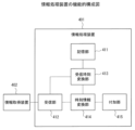
図1は、複数のセンサから情報を収集する、従来の情報処理システムの構成例を示している。図1の情報処理システムは、情報処理装置101、センサ102-1、及びセンサ102-2を含む。情報処理装置101は、FPGA(Field-Programmable Gate Array)111を含む。
FIG. 1 shows a configuration example of a conventional information processing system that collects information from multiple sensors. The information processing system of FIG. 1 includes an
センサ102-1及びセンサ102-2は、個別のタイミング信号に同期して動作する。センサ102-1は、データ121-1~データ121-4を取得し、取得したデータをバッファリングしながら情報処理装置101へ送信する。同様に、センサ102-2は、データ122-1~データ122-4を取得し、取得したデータをバッファリングしながら情報処理装置101へ送信する。
Sensor 102-1 and sensor 102-2 operate in synchronization with separate timing signals. The sensor 102-1 acquires the data 121-1 to 121-4, and transmits the acquired data to the
FPGA111は、センサ102-1からデータ121-1~データ121-4を受信し、センサ102-2からデータ122-1~データ122-4を受信する。そして、FPGA111は、受信したデータに対する情報処理を行う。
The
センサに関連して、複数のセンサによる計測結果同士を時間的に対応付けるセンサ情報処理装置、及びセンサデータに関する誤差の少ないタイムスタンプが得られるセンシングシステムが知られている(例えば、特許文献1及び特許文献2を参照)。
In relation to sensors, a sensor information processing device that temporally associates measurement results from a plurality of sensors, and a sensing system that obtains a time stamp with little error regarding sensor data are known (for example,
情報処理装置において複数のセンサから収集した情報を処理する際に、各情報に時刻を示すタイムスタンプを付加する場合がある。しかし、各センサが個別のタイミング信号に同期して動作している場合、複数のセンサのタイミング信号に基づく時刻は互いに同期しておらず、情報処理装置のシステム時刻とも同期していない。 2. Description of the Related Art When processing information collected from a plurality of sensors in an information processing apparatus, a time stamp indicating time may be added to each piece of information. However, when each sensor operates in synchronization with an individual timing signal, the times based on the timing signals of the plurality of sensors are not synchronized with each other, nor are they synchronized with the system time of the information processing apparatus.
なお、時刻同期の問題は、複数のセンサから情報を収集する場合に限らず、単一のセンサから情報を収集する場合においても生ずるものである。 Note that the problem of time synchronization occurs not only when information is collected from a plurality of sensors, but also when information is collected from a single sensor.
1つの側面において、本発明は、情報取得装置が情報を取得した時刻を、取得された情報を処理する情報処理装置のシステム時刻と同期させることを目的とする。 In one aspect, an object of the present invention is to synchronize the time at which an information acquisition device acquires information with the system time of an information processing device that processes the acquired information.
1つの案では、情報処理装置は、記憶部、受信部、受信時刻変換部、時刻情報変換部、及び付加部を含む。 In one proposal, the information processing device includes a storage unit, a reception unit, a reception time conversion unit, a time information conversion unit, and an addition unit.
記憶部は、第1システム時刻を記憶する。受信部は、記憶部に第1システム時刻が書き込まれた後に、情報取得装置から、情報取得装置が取得した第1情報と、第1情報の取得時刻を示す第1時刻情報とを受信する。そして、受信部は、第1情報と第1時刻情報とを受信した後に、情報取得装置から、第2情報と第2情報の取得時刻を示す第2時刻情報とを受信する。 The storage unit stores the first system time. The receiving unit receives the first information acquired by the information acquisition device and the first time information indicating the acquisition time of the first information from the information acquisition device after the first system time is written in the storage unit. After receiving the first information and the first time information, the receiving unit receives the second information and the second time information indicating the acquisition time of the second information from the information acquisition device.
受信時刻変換部は、第1システム時刻に基づいて、受信部が第1情報と第1時刻情報とを受信した受信時刻を、第2システム時刻に変換し、時刻情報変換部は、第2システム時刻と第1時刻情報とに基づいて、第2時刻情報を第3システム時刻に変換する。付加部は、第2システム時刻を第1情報に付加し、第3システム時刻を第2情報に付加する。 The reception time converter converts the reception time at which the receiver receives the first information and the first time information into the second system time based on the first system time, and the time information converter converts the second system time The second time information is converted into a third system time based on the time and the first time information. The adding unit adds the second system time to the first information and adds the third system time to the second information.
実施形態によれば、情報取得装置が情報を取得した時刻を、取得された情報を処理する情報処理装置のシステム時刻と同期させることができる。 According to the embodiment, the time at which the information acquisition device acquires information can be synchronized with the system time of the information processing device that processes the acquired information.
以下、図面を参照しながら、実施形態を詳細に説明する。
図2は、データにタイムスタンプを付加するFPGAの第1の比較例を示している。図2のFPGA201は、割り込みコントローラ211、MMIO(Memory-mapped Input Output)レジスタ212、及び検出部213を含む。
Hereinafter, embodiments will be described in detail with reference to the drawings.
FIG. 2 shows a first comparative example of an FPGA that adds time stamps to data. The FPGA 201 of FIG. 2 includes an
検出部213は、センサから入力データを受信すると、割り込みコントローラ211へ検出信号を出力する。割り込みコントローラ211は、検出信号を受信すると、オペレーティングシステム(Operating System,OS)202に対して、割り込み又はポーリングにより時刻同期を要求する。OS202は、割り込みコントローラ211からの要求に基づいてOS時刻221を取得し、FPGA201のMMIOレジスタ212に書き込む。OS時刻221は、システム時刻の一例である。
The
FPGA201は、MMIOレジスタ212に書き込まれたOS時刻221を、タイムスタンプとして、検出部213から出力される入力データに付加し、タイムスタンプが付加された出力データを出力する。
The FPGA 201 adds the OS time 221 written in the
しかしながら、図2の構成では、出力データのタイムスタンプは、FPGA201が入力データを受信したときのOS時刻を示しており、センサが入力データを取得したときのOS時刻を示していない。 However, in the configuration of FIG. 2, the time stamp of the output data indicates the OS time when the FPGA 201 received the input data, and does not indicate the OS time when the sensor acquired the input data.
図3は、データにタイムスタンプを付加するFPGAの第2の比較例を示している。図3のFPGA301は、MMIOレジスタ311及び加算部312を含む。
FIG. 3 shows a second comparative example of an FPGA that adds time stamps to data. The
センサは、タイミング信号に同期してカウント値をインクリメントするカウンタを含み、入力データを取得したときのカウント値をその入力データに付加して、FPGA301へ送信する。
The sensor includes a counter that increments the count value in synchronization with the timing signal, adds the count value when the input data is acquired, and transmits the input data to the
OS202は、定期的にOS時刻221を取得し、FPGA301のMMIOレジスタ311に書き込む。FPGA301は、MMIOレジスタ311にOS時刻221が書き込まれると、リセット信号をセンサへ送信し、センサは、リセット信号を受信すると、カウンタをリセットする。
The
FPGA301は、センサから入力データを受信すると、入力データからカウント値を取得する。加算部312は、MMIOレジスタ311に書き込まれたOS時刻221に、カウント値が示す時間を加算することで、タイムスタンプを生成する。そして、FPGA301は、生成されたタイムスタンプを入力データに付加し、タイムスタンプが付加された出力データを出力する。
FPGA301 will acquire a count value from input data, if input data is received from a sensor. The
しかしながら、図3の構成では、入力データに付加されたカウント値に、FPGA301からセンサへリセット信号を送信する通信のオーバヘッドが含まれている。このため、そのカウント値から生成されるタイムスタンプは、必ずしも、センサが入力データを取得したときのOS時刻を示していない。
However, in the configuration of FIG. 3, the count value added to the input data includes communication overhead for transmitting a reset signal from the
図4は、実施形態の情報処理装置の機能的構成例を示している。図4の情報処理装置401は、記憶部411、受信部412、受信時刻変換部413、時刻情報変換部414、及び付加部415を含む。記憶部411は、第1システム時刻を記憶する。
FIG. 4 shows a functional configuration example of the information processing apparatus according to the embodiment. The
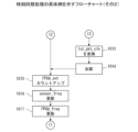
図5は、図4の情報処理装置401が行う時刻同期処理の例を示すフローチャートである。まず、受信部412は、記憶部411に第1システム時刻が書き込まれた後に、情報取得装置402から、情報取得装置402が取得した第1情報と、第1情報の取得時刻を示す第1時刻情報とを受信する(ステップ501)。そして、受信部412は、第1情報と第1時刻情報とを受信した後に、情報取得装置402から、第2情報と第2情報の取得時刻を示す第2時刻情報とを受信する(ステップ502)。
FIG. 5 is a flowchart showing an example of time synchronization processing performed by the
受信時刻変換部413は、第1システム時刻に基づいて、受信部412が第1情報と第1時刻情報とを受信した受信時刻を、第2システム時刻に変換する(ステップ503)。時刻情報変換部414は、第2システム時刻と第1時刻情報とに基づいて、第2時刻情報を第3システム時刻に変換する(ステップ504)。そして、付加部415は、第2システム時刻を第1情報に付加し(ステップ505)、第3システム時刻を第2情報に付加する(ステップ506)。
The
図4の情報処理装置401によれば、情報取得装置が情報を取得した時刻を、取得された情報を処理する情報処理装置のシステム時刻と同期させることができる。
According to the
図6は、実施形態の情報処理システムの構成例を示している。図6の情報処理システムは、情報処理装置601と情報取得装置602-1~情報取得装置602-N(Nは1以上の整数)を含む。情報処理装置601及び各情報取得装置602-i(i=1~N)は、図4の情報処理装置401及び情報取得装置402にそれぞれ対応する。情報処理装置601と各情報取得装置602-iは、通信ネットワーク603を介して通信することができる。
FIG. 6 shows a configuration example of an information processing system according to the embodiment. The information processing system of FIG. 6 includes an
情報取得装置602-iは、各種センサ、撮像装置、マイクロフォン等を含み、所定の情報を取得する。例えば、情報取得装置602-iが圧力センサを含む場合、気圧、水圧等を示す情報が取得され、情報取得装置602-iが温度センサを含む場合、温度を示す情報が取得される。情報取得装置602-iが撮像装置を含む場合、画像情報が取得され、情報取得装置602-iがマイクロフォンを含む場合、音声情報が取得される。情報取得装置602-iに含まれるセンサは、湿度センサ、風力センサ等であってもよい。 The information acquisition device 602-i includes various sensors, imaging devices, microphones, etc., and acquires predetermined information. For example, when the information acquisition device 602-i includes a pressure sensor, information indicating air pressure, water pressure, etc. is obtained, and when the information acquisition device 602-i includes a temperature sensor, information indicating temperature is obtained. If the information acquisition device 602-i includes an imaging device, image information is acquired, and if the information acquisition device 602-i includes a microphone, audio information is acquired. The sensors included in information acquisition device 602-i may be humidity sensors, wind sensors, and the like.
情報取得装置602-iは、取得した情報に、その情報の取得時刻を示す時刻情報を付加することで、センサデータのパケットを生成し、生成したパケットを情報処理装置601へ送信する。情報取得装置602-iは、タイミング信号を用いて時刻情報を生成する。
The information acquisition device 602 - i generates a sensor data packet by adding time information indicating the acquisition time of the information to the acquired information, and transmits the generated packet to the
情報処理装置601は、CPU(Central Processing Unit)611、メモリ612、及び時刻同期部613を含む。CPU611(プロセッサ)は、NTP(Network Time Protocol)によって定期的に更新されるOS時刻を、時刻同期部613へ出力する。
The
時刻同期部613は、CPU611が出力するOS時刻に基づいて、情報取得装置602-iから受信したパケットに含まれる所定の情報に、その情報の取得時刻を示すOS時刻を付加することで、転送データを生成する。そして、時刻同期部613は、生成した転送データをメモリ612へ転送し、メモリ612は、転送された転送データを記憶する。CPU611は、メモリ612が記憶している転送データに対する情報処理を行う。
Based on the OS time output by the
時刻同期部613は、受信部621、第1周波数計算部622-1~第1周波数計算部622-N、第1周波数計算部623、変換部624-1~変換部624-N、及び付加部625を含む。受信部621及び付加部625は、図4の受信部412及び付加部415にそれぞれ対応する。
The
受信部621は、情報取得装置602-iからパケットを受信し、パケットに含まれる所定の情報を付加部625へ出力し、パケットに含まれる時刻情報を、第1周波数計算部622-i及び変換部624-iへ出力する。
The receiving
第2周波数計算部623は、CPU611が出力するOS時刻と、時刻同期部613内のクロック信号とを用いて、そのクロック信号の周波数を計算する。そして、第2周波数計算部623は、計算したクロック信号の周波数を、第1周波数計算部622-1~第1周波数計算部622-N及び変換部624-1~変換部624-Nへ出力する。
The second
第1周波数計算部622-iは、2つのパケットに含まれる時刻情報の差分と、時刻同期部613内のクロック信号と、第2周波数計算部623が出力する、クロック信号の周波数とを用いて、情報取得装置602-i内のタイミング信号の周波数を計算する。そして、第1周波数計算部622-iは、計算したタイミング信号の周波数を変換部624-iへ出力する。
The first frequency calculation unit 622-i uses the difference in the time information contained in the two packets, the clock signal in the
変換部624-iは、CPU611が出力するOS時刻に基づいて、受信部412が出力する時刻情報をOS時刻に変換し、そのOS時刻を付加部625へ出力する。付加部625は、変換部624-iが出力するOS時刻を、受信部412が出力する所定の情報にタイムスタンプとして付加することで、転送データを生成し、メモリ612へ転送する。
Conversion unit 624 - i converts the time information output by
図7は、情報取得装置602-iの一例であるセンサモジュールの構成例を示している。図7のセンサモジュール701は、圧力センサ711、水晶振動子712、AD(Analog-to-Digital)コンバータ713、カウンタ714、書き込み回路715、データバッファ716、及びI2C(Inter-Integrated Circuit)バスマスタ717を含む。この場合、図6の通信ネットワーク603としてI2Cバスが用いられる。
FIG. 7 shows a configuration example of a sensor module, which is an example of the information acquisition device 602-i. A
圧力センサ711は、圧力を示すアナログ信号をADコンバータ713へ出力し、水晶振動子712は、正弦波のタイミング信号をADコンバータ713、カウンタ714、及びI2Cバスマスタ717へ出力する。
The
カウンタ714は、水晶振動子712が出力するタイミング信号に同期してカウント動作を行い、カウント値を書き込み回路715へ出力する。カウント値は、情報の取得時刻を示す時刻情報の一例である。ADコンバータ713は、水晶振動子712が出力するタイミング信号に同期して、圧力センサ711が出力するアナログ信号をデジタル信号の情報721に変換し、書き込み回路715へ出力する。
The
書き込み回路715は、ADコンバータ713が出力する情報721に、カウンタ714が出力するカウント値を付加することで、センサデータのパケットを生成して、データバッファ716へ出力する。データバッファ716は、複数のパケットをバッファリングして、I2Cバスマスタ717へ出力する。
The
I2Cバスマスタ717は、水晶振動子712が出力するタイミング信号に同期して動作し、データバッファ716が出力するパケットを、シリアルデータSDAとして情報処理装置601へ送信する。I2Cバスマスタ717は、シリアルデータSDAとともに、シリアルクロックSCLを情報処理装置601へ送信する。
The
図8は、情報取得装置602-iの一例であるビデオモジュールの構成例を示している。図8のビデオモジュール801は、撮像装置811、水晶振動子812、ADコンバータ813、カウンタ814、書き込み回路815、及びデータバッファ816を含む。
FIG. 8 shows a configuration example of a video module, which is an example of the information acquisition device 602-i. A
撮像装置811は、画像センサを含み、デジタル映像を撮影して、VGA(Video Graphics Array)信号をADコンバータ813へ出力する。VGA信号は、Hsync(Horizontal synchronizing signal)、Vsync(Vertical synchronizing signal)、blueビデオ信号、greenビデオ信号、及びredビデオ信号を含む。Hsyncは、書き込み回路815にも出力される。水晶振動子812は、正弦波のタイミング信号をカウンタ814へ出力する。
The
カウンタ814は、水晶振動子812が出力するタイミング信号に同期してカウント動作を行い、カウント値を書き込み回路815へ出力する。ADコンバータ813は、撮像装置811が出力するVGA信号をデジタル信号の画像情報821に変換し、書き込み回路815へ出力する。ADコンバータ813の代わりに、デジタルエンコーダを用いてもよい。
The
書き込み回路815は、Hsyncに同期して動作し、ADコンバータ813が出力する画像情報821に、カウンタ814が出力するカウント値を付加することで、センサデータのパケットを生成して、データバッファ816へ出力する。データバッファ816は、複数のパケットをバッファリングして、情報処理装置601へ送信する。
The
図6の時刻同期部613は、ハードウェア制御又はソフトウェア制御によって実現される。ハードウェア制御による時刻同期部613としては、FPGAのようなハードウェア論理回路が用いられ、ソフトウェア制御による時刻同期部613としては、コンピュータが用いられる。
The
以下では、図9~図17を参照しながら、時刻同期部613としてFPGAを用いた場合の構成及び動作を説明する。
The configuration and operation when an FPGA is used as the
図9は、図6の変換部624-iの構成例を示している。図9の変換部624-iは、書き込み回路901、判定回路902、セレクタ903、カウンタ904、レジスタ905~レジスタ911、及び減算器(sub)912を含む。変換部624-iは、さらに、DSP(Digital Signal Processor)913、DSP914、加算器(add)915、及び加算器916を含む。
FIG. 9 shows a configuration example of the conversion unit 624-i in FIG. 9 includes a
レジスタ905は、図4の記憶部411に対応し、DSP913及び加算器915は、受信時刻変換部413に対応し、減算器912、DSP914、及び加算器916は、時刻情報変換部414に対応する。減算器912は減算部の一例であり、DSP914は第1差分計算部の一例であり、加算器916は第1加算部の一例である。DSP913は第2差分計算部の一例であり、加算器915は第2加算部の一例である。
A
書き込み回路901は、CPU611が出力するOS時刻であるOS_system_timeを受信すると、OS_system_timeをOS_timeとしてレジスタ905に書き込む。レジスタ905は、OS_timeを加算器915へ出力する。
Upon receiving OS_system_time, which is the OS time output from the
そして、書き込み回路901は、カウンタ904をクリアして、カウント値FPGA_cntに0を設定し、レジスタ909が記憶するフラグfirst_pktflagをクリアして、first_pktflagに論理“0”を設定する。その後、カウンタ904は、時刻同期部613内のクロック信号FPGA_clkに同期してカウント動作を行い、カウント値FPGA_cntをレジスタ906へ出力する。
Then, the
受信部621は、情報取得装置602-iからパケットを受信したとき、パケットの受信を示す信号sensor_validと、パケットに含まれるカウント値sensor_cntとを、第1周波数計算部622-i及び変換部624-iへ出力する。sensor_valid及びsensor_cntは、判定回路902及びセレクタ903にそれぞれ入力される。
Upon receiving a packet from the information acquisition device 602-i, the
判定回路902は、sensor_validを受信した場合、レジスタ909のfirst_pktflagをチェックする。first_pktflagが論理“0”である場合、判定回路902は、first_pktflagに論理“1”を設定し、カウンタ904が出力するFPGA_cntを、1st_pkt_clkとしてレジスタ906に書き込む。
The
したがって、OS_system_timeがレジスタ905に書き込まれた後、受信部621が最初のパケットを受信したときに、first_pktflagに論理“1”が設定され、そのときのFPGA_cntが1st_pkt_clkに設定される。1st_pkt_clkは、最初のパケットを受信した受信時刻を示している。レジスタ906は、1st_pkt_clkをDSP913へ出力する。
Therefore, when the receiving
次に、判定回路902は、セレクタ903にレジスタ907を選択させ、セレクタ903は、sensor_cntをレジスタ907へ出力し、レジスタ907は、sensor_cntを1st_pkt_cntとして記憶する。そして、判定回路902は、セレクタ903にレジスタ908を選択させ、セレクタ903は、sensor_cntをレジスタ908へ出力し、レジスタ908は、sensor_cntをcur_pkt_cntとして記憶する。
Next,
したがって、受信部621が最初のパケットを受信したとき、そのパケットのsensor_cntが、1st_pkt_cnt及びcur_pkt_cntに設定される。
Therefore, when the
一方、first_pktflagが論理“1”である場合、判定回路902は、セレクタ903にレジスタ908を選択させ、レジスタ908は、sensor_cntをcur_pkt_cntとして記憶する。この場合、first_pktflag、1st_pkt_clk、及び1st_pkt_cntは更新されない。
On the other hand, when first_pktflag is logic "1",
したがって、OS_system_timeがレジスタ905に書き込まれた後、受信部621が2番目以降のパケットを受信したとき、そのパケットのsensor_cntがcur_pkt_cntに設定され、1st_pkt_clk及び1st_pkt_cntは変化しない。
Therefore, when the
このように、1st_pkt_cntは、最初のパケットのsensor_cntを表し、cur_pkt_cntは、最初のパケット又は2番目以降のパケットのsensor_cntを表す。レジスタ907及びレジスタ908は、1st_pkt_cnt及びcur_pkt_cntをそれぞれ減算器912へ出力する。減算器912は、cur_pkt_cntから1st_pkt_cntを減算することで、カウント値の差分を求め、DSP914へ出力する。
Thus, 1st_pkt_cnt represents the sensor_cnt of the first packet, and cur_pkt_cnt represents the sensor_cnt of the first packet or the second and subsequent packets.
したがって、受信部621が最初のパケットを受信したとき、減算器912は、カウント値の差分として0を出力する。一方、受信部621が2番目以降のパケットを受信したとき、減算器912は、受信したパケットのsensor_cntと最初のパケットのsensor_cntとの差分を出力する。
Therefore, when the
第2周波数計算部623は、クロック信号FPGA_clkの周波数FPGA_freqを、第1周波数計算部622-1~第1周波数計算部622-N及び変換部624-1~変換部624-Nへ出力する。レジスタ910は、FPGA_freqを記憶し、DSP913へ出力する。
The
第1周波数計算部622-iは、情報取得装置602-i内のタイミング信号の周波数sensor_freqを変換部624-iへ出力する。レジスタ911は、sensor_freqを記憶し、DSP914へ出力する。
The first frequency calculator 622-i outputs the frequency sensor_freq of the timing signal in the information acquisition device 602-i to the converter 624-i.
DSP913は、レジスタ906が出力する1st_pkt_clkと、レジスタ910が出力するFPGA_freqとを用いて、受信部621が最初のパケットを受信したときのOS時刻と、レジスタ905が記憶するOS_timeとの差分を計算する。DSP913は、1st_pkt_clkをFPGA_freqで除算することで、差分を求めることができる。そして、DSP913は、計算した差分を加算器915へ出力する。
The
加算器915は、DSP913が出力する差分を、レジスタ905が出力するOS_timeに加算することで、受信部621が最初のパケットを受信したときのOS時刻を求め、加算器916へ出力する。このように、DSP913及び加算器915によって、1st_pkt_clkを、最初のパケットの受信時刻を示すOS時刻に変換することができる。
The
DSP914は、レジスタ911が出力するsensor_freqを用いて、減算器912が出力するカウント値の差分から、受信したパケットのsensor_cntと最初のパケットのsensor_cntとの差分に対応する、OS時刻の差分を計算する。DSP914は、カウント値の差分をsensor_freqで除算することで、OS時刻の差分を求めることができる。そして、DSP914は、計算した差分を加算器916へ出力する。
The
DSP914が出力するOS時刻の差分は、sensor_cntの差分をsensor_freqに基づいて変換した値であるため、情報取得装置602-iと時刻同期部613との間におけるパケットの転送時間を含んでいない。したがって、通信ネットワーク603の転送遅延とは無関係である。
The OS time difference output by the
加算器916は、DSP914が出力する差分を、加算器915が出力するOS時刻に加算することで、最初のパケットの受信時刻を示すOS時刻から、sensor_cntの差分に対応する相対時間が経過した後のOS時刻を求める。そして、加算器916は、求めたOS時刻をReal_timeとして付加部625へ出力する。
The
このように、減算器912、DSP914、及び加算器916によって、受信したパケットのsensor_cntを、そのパケットに含まれる情報の取得時刻を示すOS時刻に変換することができる。加算器916が出力するReal_timeは、受信したパケットに含まれる情報にタイムスタンプとして付加される。
Thus, the
図10A及び図10Bは、図9の変換部624-iが行う時刻同期処理の具体例を示すフローチャートである。まず、書き込み回路901は、CPU611からOS_system_timeを受信したか否かをチェックする(ステップ1001)。
10A and 10B are flowcharts showing a specific example of the time synchronization processing performed by the converter 624-i in FIG. First, the
OS_system_timeを受信した場合(ステップ1001,YES)、書き込み回路901は、OS_system_timeをOS_timeとしてレジスタ905に書き込む(ステップ1003)。そして、書き込み回路901は、カウンタ904のFPGA_cntをクリアし(ステップ1004)、レジスタ909のfirst_pktflagをクリアする(ステップ1005)。
When OS_system_time is received (
次に、判定回路902は、受信部621からsensor_validを受信したか否かをチェックする(ステップ1002)。sensor_validを受信した場合(ステップ1002,YES)、判定回路902は、レジスタ909のfirst_pktflagをチェックする(ステップ1006)。
Next, the
first_pktflagが論理“0”である場合(ステップ1006,YES)、判定回路902は、first_pktflagに論理“1”を設定する(ステップ1009)。そして、判定回路902は、カウンタ904が出力するFPGA_cntを、1st_pkt_clkとしてレジスタ906に書き込む(ステップ1010)。
If first_pktflag is logic "0" (
次に、セレクタ903は、sensor_cntをレジスタ907へ出力し、レジスタ907は、sensor_cntを1st_pkt_cntとして記憶する(ステップ1011)。そして、セレクタ903は、sensor_cntをレジスタ908へ出力し、レジスタ908は、sensor_cntをcur_pkt_cntとして記憶する(ステップ1007)。
Next,
次に、減算器912は、cur_pkt_cntから1st_pkt_cntを減算することで、カウント値の差分を求める(ステップ1008)。そして、DSP914は、レジスタ911のsensor_freqを用いて、減算器912が出力するカウント値の差分をOS時刻の差分に変換する(ステップ1012)。
Next, the
次に、DSP913は、レジスタ910のFPGA_freqを用いて、レジスタ906の1st_pkt_clkを、受信部621が最初のパケットを受信したときのOS時刻と、レジスタ905のOS_timeとの差分に変換する(ステップ1013)。
Next, the
次に、加算器915は、DSP913が出力する差分を、レジスタ905のOS_timeに加算し、加算器916は、DSP914が出力する差分を、加算器915が出力する加算結果に加算する(ステップ1014)。これにより、Real_timeが求められる。
Next, the
次に、カウンタ904は、FPGA_cntをカウントアップする(ステップ1015)。そして、変換部624-iは、レジスタ911のsensor_freqを更新し(ステップ1016)、レジスタ910のFPGA_freqを更新して(ステップ1017)、ステップ1001以降の処理を繰り返す。
Next, the
OS_system_timeを受信していない場合(ステップ1001,NO)、変換部624-iは、ステップ1002以降の処理を行う。first_pktflagが論理“1”である場合(ステップ1006,NO)、変換部624-iは、ステップ1007以降の処理を行う。sensor_validを受信していない場合(ステップ1002,NO)、変換部624-iは、ステップ1015以降の処理を行う。
If OS_system_time has not been received (
図11は、図9の変換部624-iが行う時刻同期処理の例を示している。CPU611は、所定のタイミングでOS_system_timeを出力し、レジスタ905のOS_timeを更新する。
FIG. 11 shows an example of time synchronization processing performed by the converter 624-i in FIG. The
図11の例では、15:00:05、15:00:10、及び15:00:16が順番にOS_timeに設定されている。タイムフレーム1101は、15:00:05から15:00:10までの区間を表し、タイムフレーム1102は、15:00:10から15:00:16までの区間を表す。
In the example of FIG. 11, 15:00:05, 15:00:10, and 15:00:16 are set to OS_time in order. A
タイムフレーム1101において、受信部621は、FPGA_cnt=50のときに最初のパケットを受信し、FPGA_cnt=71のときに2番目のパケットを受信し、FPGA_cnt=125のときに3番目のパケットを受信する。最初のパケットのsensor_cntは1010であり、2番目のパケットのsensor_cntは1050であり、3番目のパケットのsensor_cntは1150である。
In
この場合、2番目のパケットのsensor_cntと最初のパケットのsensor_cntとの差分“40”が、OS時刻の差分1111に変換される。そして、FPGA_cnt=50に対応するOS時刻に差分1111が加算されて、sensor_cnt=1050に対応するReal_timeが求められる。
In this case, the difference “40” between the sensor_cnt of the second packet and the sensor_cnt of the first packet is converted to the
また、3番目のパケットのsensor_cntと最初のパケットのsensor_cntとの差分“140”が、OS時刻の差分1112に変換される。そして、FPGA_cnt=50に対応するOS時刻に差分1112が加算されて、sensor_cnt=1150に対応するReal_timeが求められる。
Also, the difference “140” between the sensor_cnt of the third packet and the sensor_cnt of the first packet is converted to the
タイムフレーム1102において、受信部621は、FPGA_cnt=36のときに最初のパケットを受信し、FPGA_cnt=73のときに2番目のパケットを受信し、FPGA_cnt=114のときに3番目のパケットを受信する。最初のパケットのsensor_cntは1213であり、2番目のパケットのsensor_cntは1255であり、3番目のパケットのsensor_cntは1291である。
In
タイムフレーム1102においても、タイムフレーム1101の場合と同様にして、各sensor_cntに対応するReal_timeが求められる。
In the
図6の情報処理システムによれば、各タイムフレーム内において受信した複数のパケットに含まれる情報に、情報取得装置602-iが情報を取得したときのOS時刻を示すタイムスタンプが付加される。複数の情報それぞれに付加されたタイムスタンプの差分は正確な相対時間を表しているため、それらの情報の取得時刻を情報処理装置601のOS時刻と同期させることができる。この場合、図3の構成のように、情報処理装置601から情報取得装置602-iへリセット信号を送信する必要はない。
According to the information processing system of FIG. 6, a time stamp indicating the OS time when the information acquisition device 602-i acquired the information is added to the information contained in the plurality of packets received within each time frame. Since the time stamp difference added to each of the plurality of pieces of information represents an accurate relative time, the acquisition time of the pieces of information can be synchronized with the OS time of the
また、各情報取得装置602-iが個別のタイミング信号に同期して動作している場合であっても、情報取得装置602-1~情報取得装置602-Nの間で、情報の取得時刻を同期させることが可能になる。 Further, even when each information acquisition device 602-i operates in synchronization with an individual timing signal, the information acquisition time can be set between the information acquisition devices 602-1 to 602-N. can be synchronized.
図12は、図6の第2周波数計算部623の構成例を示している。図12の第2周波数計算部623は、書き込み回路1201、ロード回路(τ)1202、カウンタ1203、レジスタ1204~レジスタ1206、減算器1207、減算器1208、DSP1209、及び統計値計算回路1210を含む。
FIG. 12 shows a configuration example of the
書き込み回路1201は、CPU611からOS_system_timeを受信すると、ロード指示をロード回路1202へ出力し、OS_system_timeをcurrent_timeとしてレジスタ1205に書き込む。レジスタ1205は、current_timeを減算器1208へ出力する。
Upon receiving OS_system_time from the
そして、書き込み回路1201は、カウンタ1203をクリアして、カウント値に0を設定する。その後、カウンタ1203は、FPGA_clkに同期してカウント動作を行い、カウント値をレジスタ1204及び減算器1207へ出力する。
Then, the
ロード回路1202は、書き込み回路1201が出力するロード指示に従って、OS_system_timeが書き込まれる直前のcurrent_timeを、last_timeとしてレジスタ1206に書き込む。レジスタ1206は、last_timeを減算器1208へ出力する。
The
また、ロード回路1202は、書き込み回路1201が出力するロード指示に従って、カウンタ1203がクリアされる直前のカウント値を、レジスタ1204に書き込む。レジスタ1204は、カウント値を減算器1207へ出力する。
Also, the
減算器1207は、レジスタ1204が出力するカウント値から、カウンタ1203が出力するカウント値を減算することで、カウント値の差分を求め、DSP1209へ出力する。減算器1208は、レジスタ1205が出力するcurrent_timeから、レジスタ1206が出力するlast_timeを減算することで、OS時刻の差分を求め、DSP1209へ出力する。
A
DSP1209は、減算器1207が出力する差分を、減算器1208が出力する差分で除算することで、FPGA_clkの周波数を求め、統計値計算回路1210へ出力する。統計値計算回路1210は、DSP1209が出力する複数の周波数の統計値を求め、求めた統計値をFPGA_freqとして出力する。統計値としては、平均値、中央値、最頻値等を用いることができる。統計値を求める必要がない場合は、統計値計算回路1210を省略してもよい。
The
図12の第2周波数計算部623によれば、環境の変化によって、時刻同期部613内のクロック信号FPGA_clkの周波数が変動する場合であっても、正確な周波数を求めることができる。そして、求められた周波数を用いることで、図9のReal_timeを補正することが可能になる。
According to the second
図13は、図6の第1周波数計算部622-iの構成例を示している。図13の第1周波数計算部622-iは、カウンタ1301、レジスタ1302~レジスタ1304、減算器1305、減算器1306、DSP1307、DSP1308、及び統計値計算回路1309を含む。
FIG. 13 shows a configuration example of the first frequency calculator 622-i in FIG. The first frequency calculator 622-i in FIG. 13 includes a
カウンタ1301は、FPGA_clkに同期してカウント動作を行い、カウント値FPGA_cur_clkをレジスタ1302及び減算器1305へ出力する。第1周波数計算部622-iは、受信部621からsensor_validを受信したとき、カウンタ1301が出力するFPGA_cur_clkを、FPGA_last_clkとしてレジスタ1302に書き込む。レジスタ1302は、FPGA_last_clkを減算器1305へ出力する。
レジスタ1303は、受信部621が出力するsensor_cntを、sensor_cur_clkとして記憶し、sensor_cur_clkを減算器1306へ出力する。第1周波数計算部622-iは、受信部621からsensor_validを受信したとき、レジスタ1303のsensor_cur_clkを、sensor_last_clkとしてレジスタ1304に書き込む。レジスタ1304は、sensor_last_clkを減算器1306へ出力する。
減算器1305は、カウンタ1301が出力するFPGA_cur_clkから、レジスタ1302が出力するFPGA_last_clkを減算することで、カウント値の差分を求め、DSP1307へ出力する。減算器1306は、レジスタ1303が出力するsensor_cur_clkから、レジスタ1304が出力するsensor_last_clkを減算することで、sensor_cntの差分を求め、DSP1307へ出力する。
DSP1307は、減算器1306が出力する差分を、減算器1305が出力する差分で除算し、除算結果をDSP1308へ出力する。DSP1308は、DSP1307が出力する除算結果に、第2周波数計算部623が出力するFPGA_freqを乗算することで、情報取得装置602-i内のタイミング信号の周波数を求め、統計値計算回路1309へ出力する。統計値計算回路1309は、DSP1308が出力する複数の周波数の統計値を求め、求めた統計値をsensor_freqとして出力する。統計値としては、平均値、中央値、最頻値等を用いることができる。統計値を求める必要がない場合は、統計値計算回路1309を省略してもよい。
The
図13の第1周波数計算部622-iによれば、環境の変化によって、情報取得装置602-i内のタイミング信号の周波数が変動する場合であっても、正確な周波数を求めることができる。そして、求められた周波数を用いることで、図9のReal_timeを補正することが可能になる。 According to the first frequency calculator 622-i in FIG. 13, even if the frequency of the timing signal in the information acquisition device 602-i fluctuates due to changes in the environment, it is possible to obtain an accurate frequency. By using the obtained frequency, Real_time in FIG. 9 can be corrected.
図14は、図12の第2周波数計算部623によって計算される、クロック信号FPGA_clkの周波数FPGA_freqの例を示している。この例では、統計値計算回路1210による統計値計算は省略されている。図14のSub出力は、減算器1207が出力するカウント値の差分を表す。FPGA_freqは、次式により計算される。
FPGA_freq
=Sub出力/(current_time-last_time) (1)
FIG. 14 shows an example of the frequency FPGA_freq of the clock signal FPGA_clk calculated by the
FPGA_freq
=Sub output/(current_time-last_time) (1)
図11の時刻同期処理において、OS_time=15:00:05のとき、Sub出力=11000である。次に、OS_time=15:00:10のとき、カウンタ1203、レジスタ1204、current_time、及びlast_timeの値は、以下のようになる。
カウンタ1203 00000
レジスタ1204 10000
current_time 15:00:10
last_time 15:00:05
In the time synchronization process of FIG. 11, Sub output=11000 when OS_time=15:00:05. Next, when OS_time=15:00:10, the values of
current_time 15:00:10
last_time 15:00:05
この場合、Sub出力=10000となり、FPGA_freqは、次式により計算される。
FPGA_freq=10000/(10-5)=2000[Hz] (2)
In this case, Sub output=10000 and FPGA_freq is calculated by the following equation.
FPGA_freq=10000/(10-5)=2000 [Hz] (2)
次に、OS_time=15:00:16のとき、カウンタ1203、レジスタ1204、current_time、及びlast_timeの値は、以下のようになる。
カウンタ1203 00000
レジスタ1204 11000
current_time 15:00:16
last_time 15:00:10
Next, when OS_time=15:00:16, the values of
register 1204 11000
current_time 15:00:16
last_time 15:00:10
この場合、Sub出力=11000となり、FPGA_freqは、次式により計算される。
FPGA_freq=11000/(16-10)=1833[Hz] (3)
In this case, Sub output=11000 and FPGA_freq is calculated by the following equation.
FPGA_freq=11000/(16-10)=1833 [Hz] (3)
図15は、図13の第1周波数計算部622-iによって計算される、タイミング信号の周波数sensor_freqの例を示している。この例では、統計値計算回路1309による統計値計算は省略されている。sensor_freqは、次式により計算される。
sensor_freq
={(sensor_cur_clk-sensor_last_clk)
/(FPGA_cur_clk-FPGA_last_clk)}
*FPGA_freq (4)
FIG. 15 shows an example of the timing signal frequency sensor_freq calculated by the first frequency calculator 622-i in FIG. In this example, statistical value calculation by the statistical
sensor_freq
= {(sensor_cur_clk-sensor_last_clk)
/(FPGA_cur_clk−FPGA_last_clk)}
*FPGA_freq (4)
図11のタイムフレーム1101において、最初のパケットを受信したとき、sensor_cnt、FPGA_cur_clk、及びFPGA_freqの値は、以下のようになる。
sensor_cnt=1010
FPGA_cur_clk=2050
FPGA_freq=2000
In
sensor_cnt=1010
FPGA_cur_clk=2050
FPGA_freq=2000
次に、2番目のパケットを受信したとき、sensor_cnt、FPGA_cur_clk、FPGA_last_clk、sensor_cur_clk、sensor_last_clk、及びFPGA_freqの値は、以下のようになる。
sensor_cnt=1050
FPGA_cur_clk=2071
FPGA_last_clk=2050
sensor_cur_clk=1050
sensor_last_clk=1010
FPGA_freq=2000
Then, when the second packet is received, the values of sensor_cnt, FPGA_cur_clk, FPGA_last_clk, sensor_cur_clk, sensor_last_clk, and FPGA_freq are as follows.
sensor_cnt=1050
FPGA_cur_clk=2071
FPGA_last_clk=2050
sensor_cur_clk=1050
sensor_last_clk=1010
FPGA_freq=2000
この場合、sensor_freqは、次式により計算される。
sensor_freq
={(1050-1010)/(2071-2050)}*2000
=3810[Hz] (5)
In this case, sensor_freq is calculated by the following equation.
sensor_freq
= {(1050-1010)/(2071-2050)}*2000
= 3810 [Hz] (5)
次に、3番目のパケットを受信したとき、sensor_cnt、FPGA_cur_clk、FPGA_last_clk、sensor_cur_clk、sensor_last_clk、及びFPGA_freqの値は、以下のようになる。
sensor_cnt=1150
FPGA_cur_clk=2125
FPGA_last_clk=2071
sensor_cur_clk=1150
sensor_last_clk=1050
FPGA_freq=2000
Then, when the third packet is received, the values of sensor_cnt, FPGA_cur_clk, FPGA_last_clk, sensor_cur_clk, sensor_last_clk, and FPGA_freq are as follows.
sensor_cnt=1150
FPGA_cur_clk=2125
FPGA_last_clk=2071
sensor_cur_clk=1150
sensor_last_clk=1050
FPGA_freq=2000
この場合、sensor_freqは、次式により計算される。
sensor_freq
={(1150-1050)/(2125-2071)}*2000
=3704[Hz] (6)
In this case, sensor_freq is calculated by the following equation.
sensor_freq
= {(1150-1050)/(2125-2071)}*2000
= 3704 [Hz] (6)
図16は、図9の変換部624-iによって計算されるOS時刻Real_timeの例を示している。Real_timeは、次式により計算される。
Real_time
=(cur_pkt_cnt-1st_pkt_cnt)/sensor_freq
+1st_pkt_clk/FPGA_freq+OS_time
(7)
FIG. 16 shows an example of the OS time Real_time calculated by the converter 624-i of FIG. Real_time is calculated by the following formula.
Real_time
= (cur_pkt_cnt-1st_pkt_cnt)/sensor_freq
+1st_pkt_clk/FPGA_freq+OS_time
(7)
図11の時刻同期処理において、OS_time=15:00:05のとき、1st_pkt_clk、first_pktflag、FPGA_freq、及びsensor_freqの値は、以下のようになる。
1st_pkt_clk=0
first_pktflag=0
FPGA_freq=2000
sensor_freq=4000
In the time synchronization process of FIG. 11, when OS_time=15:00:05, the values of 1st_pkt_clk, first_pktflag, FPGA_freq, and sensor_freq are as follows.
1st_pkt_clk=0
first_pktflag=0
FPGA_freq=2000
sensor_freq=4000
次に、最初のパケットを受信したとき、sensor_cnt、1st_pkt_clk、first_pktflag、1st_pkt_cnt、cur_pkt_cnt、FPGA_freq、及びsensor_freqの値は、以下のようになる。
sensor_cnt=1010
1st_pkt_clk=50
first_pktflag=1
1st_pkt_cnt=1010
cur_pkt_cnt=1010
FPGA_freq=2000
sensor_freq=4000
Then, when the first packet is received, the values of sensor_cnt, 1st_pkt_clk, first_pktflag, 1st_pkt_cnt, cur_pkt_cnt, FPGA_freq, and sensor_freq are as follows.
sensor_cnt=1010
1st_pkt_clk=50
first_pktflag=1
1st_pkt_cnt=1010
cur_pkt_cnt=1010
FPGA_freq=2000
sensor_freq=4000
この場合、Real_timeは、次式により計算される。
Real_time
=(1010-1010)/4000+50/2000+15:00:05
=15:00:05:025 (8)
In this case, Real_time is calculated by the following equation.
Real_time
=(1010-1010)/4000+50/2000+15:00:05
= 15:00:05:025 (8)
次に、2番目のパケットを受信したとき、sensor_cnt、1st_pkt_clk、first_pktflag、1st_pkt_cnt、cur_pkt_cnt、FPGA_freq、及びsensor_freqの値は、以下のようになる。
sensor_cnt=1050
1st_pkt_clk=50
first_pktflag=1
1st_pkt_cnt=1010
cur_pkt_cnt=1050
FPGA_freq=2000
sensor_freq=3810
Then, when the second packet is received, the values of sensor_cnt, 1st_pkt_clk, first_pktflag, 1st_pkt_cnt, cur_pkt_cnt, FPGA_freq, and sensor_freq are as follows.
sensor_cnt=1050
1st_pkt_clk=50
first_pktflag=1
1st_pkt_cnt=1010
cur_pkt_cnt=1050
FPGA_freq=2000
sensor_freq=3810
この場合、Real_timeは、次式により計算される。
Real_time
=(1050-1010)/3810+50/2000+15:00:05
=15:00:05:035 (9)
In this case, Real_time is calculated by the following equation.
Real_time
=(1050-1010)/3810+50/2000+15:00:05
= 15:00:05:035 (9)
次に、3番目のパケットを受信したとき、sensor_cnt、1st_pkt_clk、first_pktflag、1st_pkt_cnt、cur_pkt_cnt、FPGA_freq、及びsensor_freqの値は、以下のようになる。
sensor_cnt=1150
1st_pkt_clk=50
first_pktflag=1
1st_pkt_cnt=1010
cur_pkt_cnt=1150
FPGA_freq=2000
sensor_freq=3704
Next, when the third packet is received, the values of sensor_cnt, 1st_pkt_clk, first_pktflag, 1st_pkt_cnt, cur_pkt_cnt, FPGA_freq, and sensor_freq are as follows.
sensor_cnt=1150
1st_pkt_clk=50
first_pktflag=1
1st_pkt_cnt=1010
cur_pkt_cnt=1150
FPGA_freq=2000
sensor_freq=3704
この場合、Real_timeは、次式により計算される。
Real_time
=(1150-1010)/3704+50/2000+15:00:05
=15:00:05:063 (10)
In this case, Real_time is calculated by the following equation.
Real_time
=(1150-1010)/3704+50/2000+15:00:05
= 15:00:05:063 (10)
ところで、通信ネットワーク603において障害等が発生した場合、情報取得装置602-iから送信されたセンサデータのパケットが消失して、情報処理装置601に到達しないことがある。このような場合であっても、時刻同期部613は、情報処理装置601に到達したパケットに含まれる情報に対して、タイムスタンプを付加することが可能である。
By the way, when a failure or the like occurs in the
図17は、通信ネットワーク603におけるパケット消失時の時刻同期処理の例を示している。図17(a)は、図11のタイムフレーム1101において、最初のパケットが消失した場合の時刻同期処理の例を示している。
FIG. 17 shows an example of time synchronization processing when packets are lost in the
図17(a)のタイムフレーム1101において、最初のパケットが消失した場合、受信部621は、FPGA_cnt=71のときに2番目のパケットを受信し、FPGA_cnt=125のときに3番目のパケットを受信する。
In the
この場合、3番目のパケットのsensor_cntと2番目のパケットのsensor_cntとの差分“100”が、OS時刻の差分1701に変換される。そして、FPGA_cnt=71に対応するOS時刻に差分1701が加算されて、sensor_cnt=1150に対応するReal_timeが求められる。
In this case, the difference “100” between the sensor_cnt of the third packet and the sensor_cnt of the second packet is converted to the
図17(b)は、図11のタイムフレーム1101において、2番目のパケットが消失した場合の時刻同期処理の例を示している。
FIG. 17(b) shows an example of time synchronization processing when the second packet is lost in the
図17(b)のタイムフレーム1101において、2番目のパケットが消失した場合、受信部621は、FPGA_cnt=50のときに最初のパケットを受信し、FPGA_cnt=125のときに3番目のパケットを受信する。
In the
この場合、3番目のパケットのsensor_cntと最初のパケットのsensor_cntとの差分“140”が、OS時刻の差分1112に変換される。そして、FPGA_cnt=50に対応するOS時刻に差分1112が加算されて、sensor_cnt=1150に対応するReal_timeが求められる。
In this case, the difference “140” between the sensor_cnt of the third packet and the sensor_cnt of the first packet is converted to the
このように、図6の情報処理システムによれば、タイムフレーム内のいずれのパケットが消失した場合であっても、いずれかのパケットを受信したOS時刻を基準として、後続するパケットに含まれる情報にタイムスタンプを付加することができる。 As described above, according to the information processing system of FIG. 6, even if any packet within the time frame is lost, the information contained in the subsequent packet is determined based on the OS time when the packet was received. can be timestamped.
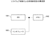
図18は、ソフトウェア制御による時刻同期部613の構成例を示している。図18の時刻同期部613は、CPU1801、メモリ1802、及びインタフェース1803を含むコンピュータである。
FIG. 18 shows a configuration example of the
メモリ1802は、例えば、ROM(Read Only Memory)、RAM(Random Access Memory)、フラッシュメモリ等の半導体メモリであり、処理に用いられるプログラム及びデータを格納する。メモリ1802は、図4の記憶部411として用いることができる。
The
CPU1801(プロセッサ)は、例えば、メモリ1802を利用してプログラムを実行することにより、図4の受信時刻変換部413、時刻情報変換部414、及び付加部415として動作する。CPU1801は、メモリ1802を利用してプログラムを実行することにより、第1周波数計算部、第2周波数計算部、減算部、第1差分計算部、第1加算部、第2差分計算部、及び第2加算部としても動作する。
The CPU 1801 (processor) operates as the reception
インタフェース1803は、通信ネットワーク603に接続され、通信に伴うデータ変換を行う通信インタフェース回路である。時刻同期部613は、プログラム及びデータを外部の装置からインタフェース1803を介して受信し、それらをメモリ1802にロードして使用することができる。インタフェース1803は、図4の受信部412又は図6の受信部621として用いることができる。
The
図18の時刻同期部613は、さらに、可搬型記録媒体を駆動する媒体駆動装置を含んでいてもよい。可搬型記録媒体は、メモリデバイス、フレキシブルディスク、光ディスク、光磁気ディスク等である。可搬型記録媒体は、CD-ROM(Compact Disk Read Only Memory)、DVD(Digital Versatile Disk)、USB(Universal Serial Bus)メモリ等であってもよい。オペレータ又はユーザは、この可搬型記録媒体にプログラム及びデータを格納しておき、それらをメモリ1802にロードして使用することができる。
The
このように、処理に用いられるプログラム及びデータを格納するコンピュータ読み取り可能な記録媒体は、メモリ1802又は可搬型記録媒体のような、物理的な(非一時的な)記録媒体である。
Thus, a computer-readable recording medium storing programs and data used for processing is a physical (non-temporary) recording medium such as
図4の情報処理装置401の構成は一例に過ぎず、情報処理装置401の用途又は条件に応じて一部の構成要素を省略又は変更してもよい。
The configuration of the
図6の情報処理システムの構成は一例に過ぎず、情報処理システムの用途又は条件に応じて一部の構成要素を省略又は変更してもよい。例えば、時刻同期部613内のクロック信号の周波数があまり変動せず、第1周波数計算部622-i及び変換部624-iがその周波数を示す固定値を保持している場合は、第2周波数計算部623を省略することができる。情報取得装置602-i内のタイミング信号の周波数があまり変動せず、変換部624-iがその周波数を示す固定値を保持している場合は、第1周波数計算部622-iを省略することができる。
The configuration of the information processing system in FIG. 6 is merely an example, and some components may be omitted or changed according to the application or conditions of the information processing system. For example, when the frequency of the clock signal in the
情報取得装置602-1~情報取得装置602-Nは、情報処理装置601内に設けられていてもよい。
Information acquisition device 602 - 1 to information acquisition device 602 -N may be provided in
図7のセンサモジュール701及び図8のビデオモジュール801の構成は一例に過ぎず、情報処理システムの用途又は条件に応じて一部の構成要素を省略又は変更してもよい。図7の圧力センサ711の代わりに、温度センサ、湿度センサ、風力センサ等を用いることもできる。
The configurations of the
図9の変換部624-i、図12の第2周波数計算部623、図13の第1周波数計算部622-i、及び図18の時刻同期部613の構成は一例に過ぎず、情報処理システムの用途又は条件に応じて一部の構成要素を省略又は変更してもよい。
The configuration of the conversion unit 624-i in FIG. 9, the second
図5、図10A、及び図10Bのフローチャートは一例に過ぎず、変換部624-iの構成又は条件に応じて一部の処理を省略又は変更してもよい。 The flowcharts of FIGS. 5, 10A, and 10B are merely examples, and some processing may be omitted or changed according to the configuration or conditions of the conversion unit 624-i.
図11及び図17に示した時刻同期処理は一例に過ぎず、sensor_cnt、FPGA_cnt、及びOS_timeは、情報取得装置602-iが取得する情報に応じて変化する。図14~図16に示した計算結果は一例に過ぎず、計算結果は、情報取得装置602-iが取得する情報に応じて変化する。 The time synchronization processing shown in FIGS. 11 and 17 is merely an example, and sensor_cnt, FPGA_cnt, and OS_time change according to information acquired by the information acquisition device 602-i. The calculation results shown in FIGS. 14 to 16 are only examples, and the calculation results change according to the information acquired by the information acquisition device 602-i.
式(1)~式(10)の計算式は一例に過ぎず、情報処理装置601の構成又は条件に応じて別の計算式を用いてもよい。
The calculation formulas (1) to (10) are merely examples, and other calculation formulas may be used according to the configuration or conditions of the
開示の実施形態とその利点について詳しく説明したが、当業者は、特許請求の範囲に明確に記載した本発明の範囲から逸脱することなく、様々な変更、追加、省略をすることができるであろう。 Although the disclosed embodiments and their advantages have been described in detail, those skilled in the art can make various modifications, additions and omissions without departing from the scope of the invention as defined in the claims. deaf.
図2乃至図18を参照しながら説明した実施形態に関し、さらに以下の付記を開示する。
(付記1)
第1システム時刻を記憶する記憶部と、
前記記憶部に前記第1システム時刻が書き込まれた後に、情報取得装置から、前記情報取得装置が取得した第1情報と、前記第1情報の取得時刻を示す第1時刻情報とを受信し、前記第1情報と前記第1時刻情報とを受信した後に、前記情報取得装置から、第2情報と前記第2情報の取得時刻を示す第2時刻情報とを受信する受信部と、
前記第1システム時刻に基づいて、前記受信部が前記第1情報と前記第1時刻情報とを受信した受信時刻を、第2システム時刻に変換する受信時刻変換部と、
前記第2システム時刻と前記第1時刻情報とに基づいて、前記第2時刻情報を第3システム時刻に変換する時刻情報変換部と、
前記第2システム時刻を前記第1情報に付加し、前記第3システム時刻を前記第2情報に付加する付加部と、
を備えることを特徴とする情報処理装置。
(付記2)
前記時刻情報変換部は、
前記第2時刻情報と前記第1時刻情報との差分を生成する減算部と、
前記第2時刻情報と前記第1時刻情報との差分から、前記第3システム時刻と前記第2システム時刻との差分を計算する第1差分計算部と、
前記第3システム時刻と前記第2システム時刻との差分を前記第2システム時刻に加算することで、前記第3システム時刻を求める第1加算部と、
を含むことを特徴とする付記1記載の情報処理装置。
(付記3)
前記第2時刻情報と前記第1時刻情報との差分と、クロック信号と、前記クロック信号の周波数とを用いて、前記情報取得装置において取得時刻を生成するタイミング信号の周波数を計算する第1周波数計算部をさらに備え、
前記受信時刻変換部は、前記受信部が前記第1情報と前記第1時刻情報とを受信したときに、前記クロック信号に基づいて特定された時刻を、前記受信時刻として用い、
前記第1差分計算部は、前記第2時刻情報と前記第1時刻情報との差分と、前記タイミング信号の周波数とを用いて、前記第3システム時刻と前記第2システム時刻との差分を計算することを特徴とする付記2記載の情報処理装置。
(付記4)
前記受信時刻変換部は、
前記受信時刻と前記クロック信号の周波数とを用いて、前記第2システム時刻と前記第1システム時刻との差分を計算する第2差分計算部と、
前記第2システム時刻と前記第1システム時刻との差分を前記第1システム時刻に加算することで、前記第2システム時刻を求める第2加算部と、
を含むことを特徴とする付記3記載の情報処理装置。
(付記5)
前記第1システム時刻と前記クロック信号とを用いて、前記クロック信号の周波数を計算する第2周波数計算部をさらに備えることを特徴とする付記4記載の情報処理装置。
(付記6)
前記受信部は、前記記憶部に前記第1システム時刻が書き込まれた後に、複数の情報取得装置のうちいずれかの情報取得装置から、前記いずれかの情報取得装置が取得した第1情報と第1時刻情報とを受信し、前記第1情報と前記第1時刻情報とを受信した後に、前記いずれかの情報取得装置から、第2情報と第2時刻情報とを受信し、
前記付加部は、前記第2システム時刻を前記いずれかの情報取得装置から受信した第1情報に付加し、前記第3システム時刻を前記いずれかの情報取得装置から受信した第2情報に付加することを特徴とする付記1乃至5のいずれか1項に記載の情報処理装置。
(付記7)
情報処理装置によって実行される時刻同期方法であって、
前記情報処理装置が、
第1システム時刻が記憶部に書き込まれた後に、情報取得装置から、前記情報取得装置が取得した第1情報と、前記第1情報の取得時刻を示す第1時刻情報とを受信し、
前記第1情報と前記第1時刻情報とを受信した後に、前記情報取得装置から、第2情報と前記第2情報の取得時刻を示す第2時刻情報とを受信し、
前記第1システム時刻に基づいて、前記第1情報と前記第1時刻情報とを受信した受信時刻を、第2システム時刻に変換し、
前記第2システム時刻と前記第1時刻情報とに基づいて、前記第2時刻情報を第3システム時刻に変換し、
前記第2システム時刻を前記第1情報に付加し、
前記第3システム時刻を前記第2情報に付加する、
ことを特徴とする時刻同期方法。
(付記8)
前記情報処理装置は、
前記第2時刻情報と前記第1時刻情報との差分を生成し、
前記第2時刻情報と前記第1時刻情報との差分から、前記第3システム時刻と前記第2システム時刻との差分を計算し、
前記第3システム時刻と前記第2システム時刻との差分を前記第2システム時刻に加算することで、前記第3システム時刻を求めることを特徴とする付記7記載の時刻同期方法。
(付記9)
前記情報処理装置は、
前記第2時刻情報と前記第1時刻情報との差分と、クロック信号と、前記クロック信号の周波数とを用いて、前記情報取得装置において取得時刻を生成するタイミング信号の周波数を計算し、
前記第1情報と前記第1時刻情報とを受信したときに、前記クロック信号に基づいて特定された時刻を、前記受信時刻として用い、
前記第2時刻情報と前記第1時刻情報との差分と、前記タイミング信号の周波数とを用いて、前記第3システム時刻と前記第2システム時刻との差分を計算することを特徴とする付記8記載の時刻同期方法。
(付記10)
前記情報処理装置は、
前記受信時刻と前記クロック信号の周波数とを用いて、前記第2システム時刻と前記第1システム時刻との差分を計算し、
前記第2システム時刻と前記第1システム時刻との差分を前記第1システム時刻に加算することで、前記第2システム時刻を求めることを特徴とする付記9記載の時刻同期方法。
(付記11)
第1システム時刻が記憶部に書き込まれた後に、情報取得装置から、前記情報取得装置が取得した第1情報と、前記第1情報の取得時刻を示す第1時刻情報とを受信し、
前記第1情報と前記第1時刻情報とを受信した後に、前記情報取得装置から、第2情報と前記第2情報の取得時刻を示す第2時刻情報とを受信し、
前記第1システム時刻に基づいて、前記第1情報と前記第1時刻情報とを受信した受信時刻を、第2システム時刻に変換し、
前記第2システム時刻と前記第1時刻情報とに基づいて、前記第2時刻情報を第3システム時刻に変換し、
前記第2システム時刻を前記第1情報に付加し、
前記第3システム時刻を前記第2情報に付加する、
処理をコンピュータに実行させるための時刻同期プログラム。
(付記12)
前記コンピュータは、
前記第2時刻情報と前記第1時刻情報との差分を生成し、
前記第2時刻情報と前記第1時刻情報との差分から、前記第3システム時刻と前記第2システム時刻との差分を計算し、
前記第3システム時刻と前記第2システム時刻との差分を前記第2システム時刻に加算することで、前記第3システム時刻を求めることを特徴とする付記11記載の時刻同期プログラム。
(付記13)
前記コンピュータは、
前記第2時刻情報と前記第1時刻情報との差分と、クロック信号と、前記クロック信号の周波数とを用いて、前記情報取得装置において取得時刻を生成するタイミング信号の周波数を計算し、
前記第1情報と前記第1時刻情報とを受信したときに、前記クロック信号に基づいて特定された時刻を、前記受信時刻として用い、
前記第2時刻情報と前記第1時刻情報との差分と、前記タイミング信号の周波数とを用いて、前記第3システム時刻と前記第2システム時刻との差分を計算することを特徴とする付記12記載の時刻同期プログラム。
(付記14)
前記コンピュータは、
前記受信時刻と前記クロック信号の周波数とを用いて、前記第2システム時刻と前記第1システム時刻との差分を計算し、
前記第2システム時刻と前記第1システム時刻との差分を前記第1システム時刻に加算することで、前記第2システム時刻を求めることを特徴とする付記13記載の時刻同期プログラム。
The following remarks are further disclosed with respect to the embodiments described with reference to FIGS.
(Appendix 1)
a storage unit that stores the first system time;
After the first system time is written in the storage unit, receiving the first information acquired by the information acquisition device and the first time information indicating the acquisition time of the first information from the information acquisition device, a receiving unit that receives second information and second time information indicating an acquisition time of the second information from the information acquisition device after receiving the first information and the first time information;
a reception time conversion unit that converts a reception time at which the reception unit receives the first information and the first time information into a second system time based on the first system time;
a time information conversion unit that converts the second time information into a third system time based on the second system time and the first time information;
an addition unit that adds the second system time to the first information and adds the third system time to the second information;
An information processing device comprising:
(Appendix 2)
The time information conversion unit
a subtraction unit that generates a difference between the second time information and the first time information;
a first difference calculation unit that calculates the difference between the third system time and the second system time from the difference between the second time information and the first time information;
a first addition unit that obtains the third system time by adding the difference between the third system time and the second system time to the second system time;
The information processing apparatus according to
(Appendix 3)
A first frequency for calculating a frequency of a timing signal for generating an acquisition time in the information acquisition device using a difference between the second time information and the first time information, a clock signal, and a frequency of the clock signal. further comprising a calculation unit,
The reception time conversion unit uses, as the reception time, the time specified based on the clock signal when the reception unit receives the first information and the first time information,
The first difference calculator calculates the difference between the third system time and the second system time using the difference between the second time information and the first time information and the frequency of the timing signal. The information processing apparatus according to Supplementary Note 2, wherein:
(Appendix 4)
The reception time conversion unit
a second difference calculator that calculates the difference between the second system time and the first system time using the reception time and the frequency of the clock signal;
a second addition unit that obtains the second system time by adding the difference between the second system time and the first system time to the first system time;
The information processing apparatus according to appendix 3, characterized by comprising:
(Appendix 5)
5. The information processing apparatus according to claim 4, further comprising a second frequency calculator that calculates the frequency of the clock signal using the first system time and the clock signal.
(Appendix 6)
After the first system time is written in the storage unit, the receiving unit receives the first information acquired by any one of the plurality of information acquisition devices from the information acquisition device and the first information acquired by the information acquisition device. receiving the first time information, and after receiving the first information and the first time information, receiving the second information and the second time information from any of the information acquisition devices;
The adding unit adds the second system time to the first information received from the information acquisition device, and adds the third system time to the second information received from the information acquisition device. The information processing apparatus according to any one of
(Appendix 7)
A time synchronization method executed by an information processing device,
The information processing device
After the first system time is written in the storage unit, receiving the first information acquired by the information acquisition device and the first time information indicating the acquisition time of the first information from the information acquisition device,
After receiving the first information and the first time information, receiving the second information and second time information indicating an acquisition time of the second information from the information acquisition device,
converting the reception time of receiving the first information and the first time information into a second system time based on the first system time;
converting the second time information into a third system time based on the second system time and the first time information;
adding the second system time to the first information;
adding the third system time to the second information;
A time synchronization method characterized by:
(Appendix 8)
The information processing device is
generating a difference between the second time information and the first time information;
calculating the difference between the third system time and the second system time from the difference between the second time information and the first time information;
8. The time synchronization method according to claim 7, wherein the third system time is obtained by adding a difference between the third system time and the second system time to the second system time.
(Appendix 9)
The information processing device is
using the difference between the second time information and the first time information, a clock signal, and the frequency of the clock signal to calculate the frequency of a timing signal for generating an acquisition time in the information acquisition device;
using the time specified based on the clock signal as the reception time when the first information and the first time information are received;
Supplementary note 8, wherein the difference between the third system time and the second system time is calculated using the difference between the second time information and the first time information and the frequency of the timing signal. Described time synchronization method.
(Appendix 10)
The information processing device is
calculating a difference between the second system time and the first system time using the received time and the frequency of the clock signal;
The time synchronization method according to claim 9, wherein the second system time is obtained by adding a difference between the second system time and the first system time to the first system time.
(Appendix 11)
After the first system time is written in the storage unit, receiving the first information acquired by the information acquisition device and the first time information indicating the acquisition time of the first information from the information acquisition device,
After receiving the first information and the first time information, receiving the second information and second time information indicating an acquisition time of the second information from the information acquisition device,
converting the reception time of receiving the first information and the first time information into a second system time based on the first system time;
converting the second time information into a third system time based on the second system time and the first time information;
adding the second system time to the first information;
adding the third system time to the second information;
A time synchronization program for executing processing on a computer.
(Appendix 12)
The computer is
generating a difference between the second time information and the first time information;
calculating the difference between the third system time and the second system time from the difference between the second time information and the first time information;
12. The time synchronization program according to
(Appendix 13)
The computer is
using the difference between the second time information and the first time information, a clock signal, and the frequency of the clock signal to calculate the frequency of a timing signal for generating an acquisition time in the information acquisition device;
using the time specified based on the clock signal as the reception time when the first information and the first time information are received;
(Appendix 14)
The computer is
calculating a difference between the second system time and the first system time using the received time and the frequency of the clock signal;
14. The time synchronization program according to
101、401、601 情報処理装置
102-1、102-2 センサ
121-1~121-4、122-1~122-4 データ
111、201、301 FPGA
202 OS
211 割り込みコントローラ
212、311 MMIOレジスタ
213 検出部
221 OS時刻
312 加算部
402、602-1~602-N 情報取得装置
411 記憶部
412、621 受信部
413 受信時刻変換部
414 時刻情報変換部
415、625 付加部
603 通信ネットワーク
611 CPU
612 メモリ
613 時刻同期部
622-1~622-N 第1周波数計算部
623 第2周波数計算部
624-1~624-N 変換部
701 センサモジュール
711 圧力センサ
712、812 水晶振動子
713、813 ADコンバータ
714、814、904、1203、1301 カウンタ
715、815、901、1201 書き込み回路
716、816 データバッファ
717 I2Cバスマスタ
721 情報
801 ビデオモジュール
811 撮像装置
821 画像情報
902 判定回路
903 セレクタ
905~911、1204~1206、1302~1304 レジスタ
912、1207、1208、1305、1306 減算器
913、914、1209、1307、1308 DSP
915、916 加算器
1101、1102 タイムフレーム
1111、1112、1701 OS時刻の差分
1202 ロード回路
1210、1309 統計値計算回路
1801 CPU
1802 メモリ
1803 インタフェース
101, 401, 601 Information processing device 102-1, 102-2 Sensor 121-1 to 121-4, 122-1 to 122-4
202 OS
211 interrupt
612
915, 916
1802
Claims (6)
前記記憶部に前記第1システム時刻が書き込まれた後に、情報取得装置から、前記情報取得装置が取得した第1情報と、前記第1情報の取得時刻を示す第1時刻情報とを受信し、前記第1情報と前記第1時刻情報とを受信した後に、前記情報取得装置から、第2情報と前記第2情報の取得時刻を示す第2時刻情報とを受信する受信部と、
前記第2時刻情報と前記第1時刻情報との差分と、クロック信号と、前記クロック信号の周波数とを用いて、前記情報取得装置において取得時刻を生成するタイミング信号の周波数を計算する第1周波数計算部と、
前記受信部が前記第1情報と前記第1時刻情報とを受信したときに、前記クロック信号に基づいて特定された時刻を、前記受信部が前記第1情報と前記第1時刻情報とを受信した受信時刻として用い、前記第1システム時刻に基づいて、前記受信時刻を第2システム時刻に変換する受信時刻変換部と、
前記第2システム時刻と前記第1時刻情報とに基づいて、前記第2時刻情報を第3システム時刻に変換する時刻情報変換部と、
前記第2システム時刻を前記第1情報に付加し、前記第3システム時刻を前記第2情報に付加する付加部と、
を備え、
前記時刻情報変換部は、
前記第2時刻情報と前記第1時刻情報との差分を生成する減算部と、
前記第2時刻情報と前記第1時刻情報との差分と、前記タイミング信号の周波数とを用いて、前記第3システム時刻と前記第2システム時刻との差分を計算する第1差分計算部と、
前記第3システム時刻と前記第2システム時刻との差分を前記第2システム時刻に加算することで、前記第3システム時刻を求める第1加算部と、
を含むことを特徴とする情報処理装置。 a storage unit that stores the first system time;
After the first system time is written in the storage unit, receiving the first information acquired by the information acquisition device and the first time information indicating the acquisition time of the first information from the information acquisition device, a receiving unit that receives second information and second time information indicating an acquisition time of the second information from the information acquisition device after receiving the first information and the first time information;
A first frequency for calculating a frequency of a timing signal for generating an acquisition time in the information acquisition device using a difference between the second time information and the first time information, a clock signal, and a frequency of the clock signal. a calculation unit;
When the receiving unit receives the first information and the first time information, the receiving unit receives the first information and the first time information at the time specified based on the clock signal. a reception time converter for converting the reception time into a second system time based on the first system time;
a time information conversion unit that converts the second time information into a third system time based on the second system time and the first time information;
an addition unit that adds the second system time to the first information and adds the third system time to the second information;
with
The time information conversion unit
a subtraction unit that generates a difference between the second time information and the first time information;
a first difference calculator that calculates the difference between the third system time and the second system time using the difference between the second time information and the first time information and the frequency of the timing signal;
a first addition unit that obtains the third system time by adding the difference between the third system time and the second system time to the second system time;
An information processing device comprising :
前記受信時刻と前記クロック信号の周波数とを用いて、前記第2システム時刻と前記第1システム時刻との差分を計算する第2差分計算部と、
前記第2システム時刻と前記第1システム時刻との差分を前記第1システム時刻に加算することで、前記第2システム時刻を求める第2加算部と、
を含むことを特徴とする請求項1記載の情報処理装置。 The reception time conversion unit
a second difference calculator that calculates the difference between the second system time and the first system time using the reception time and the frequency of the clock signal;
a second addition unit that obtains the second system time by adding the difference between the second system time and the first system time to the first system time;
2. The information processing apparatus according to claim 1 , comprising:
前記付加部は、前記第2システム時刻を前記いずれかの情報取得装置から受信した第1情報に付加し、前記第3システム時刻を前記いずれかの情報取得装置から受信した第2情報に付加することを特徴とする請求項1乃至3のいずれか1項に記載の情報処理装置。 After the first system time is written in the storage unit, the receiving unit receives the first information acquired by any one of the plurality of information acquisition devices from the information acquisition device and the first information acquired by the information acquisition device. receiving the first time information, and after receiving the first information and the first time information, receiving the second information and the second time information from any of the information acquisition devices;
The adding unit adds the second system time to the first information received from the information acquisition device, and adds the third system time to the second information received from the information acquisition device. 4. The information processing apparatus according to any one of claims 1 to 3 , characterized by:
前記情報処理装置が、
第1システム時刻が記憶部に書き込まれた後に、情報取得装置から、前記情報取得装置が取得した第1情報と、前記第1情報の取得時刻を示す第1時刻情報とを受信し、
前記第1情報と前記第1時刻情報とを受信した後に、前記情報取得装置から、第2情報と前記第2情報の取得時刻を示す第2時刻情報とを受信し、
前記第2時刻情報と前記第1時刻情報との差分と、クロック信号と、前記クロック信号の周波数とを用いて、前記情報取得装置において取得時刻を生成するタイミング信号の周波数を計算し、
前記第1情報と前記第1時刻情報とを受信したときに、前記クロック信号に基づいて特定された時刻を、前記第1情報と前記第1時刻情報とを受信した受信時刻として用い、前記第1システム時刻に基づいて、前記受信時刻を第2システム時刻に変換し、
前記第2時刻情報と前記第1時刻情報との差分と、前記タイミング信号の周波数とを用いて、前記第3システム時刻と前記第2システム時刻との差分を計算し、
前記第3システム時刻と前記第2システム時刻との差分を前記第2システム時刻に加算することで、第3システム時刻を求め、
前記第2システム時刻を前記第1情報に付加し、
前記第3システム時刻を前記第2情報に付加する、
ことを特徴とする時刻同期方法。 A time synchronization method executed by an information processing device,
The information processing device
After the first system time is written in the storage unit, receiving the first information acquired by the information acquisition device and the first time information indicating the acquisition time of the first information from the information acquisition device,
After receiving the first information and the first time information, receiving the second information and second time information indicating an acquisition time of the second information from the information acquisition device,
using the difference between the second time information and the first time information, a clock signal, and the frequency of the clock signal to calculate the frequency of a timing signal for generating an acquisition time in the information acquisition device;
When the first information and the first time information are received, the time specified based on the clock signal is used as the reception time when the first information and the first time information are received, and the first information and the first time information are received . Converting the received time to a second system time based on one system time;
calculating the difference between the third system time and the second system time using the difference between the second time information and the first time information and the frequency of the timing signal;
Obtaining a third system time by adding the difference between the third system time and the second system time to the second system time ,
adding the second system time to the first information;
adding the third system time to the second information;
A time synchronization method characterized by:
前記第1情報と前記第1時刻情報とを受信した後に、前記情報取得装置から、第2情報と前記第2情報の取得時刻を示す第2時刻情報とを受信し、
前記第2時刻情報と前記第1時刻情報との差分と、クロック信号と、前記クロック信号の周波数とを用いて、前記情報取得装置において取得時刻を生成するタイミング信号の周波数を計算し、
前記第1情報と前記第1時刻情報とを受信したときに、前記クロック信号に基づいて特定された時刻を、前記第1情報と前記第1時刻情報とを受信した受信時刻として用い、前記第1システム時刻に基づいて、前記受信時刻を第2システム時刻に変換し、
前記第2時刻情報と前記第1時刻情報との差分と、前記タイミング信号の周波数とを用いて、前記第3システム時刻と前記第2システム時刻との差分を計算し、
前記第3システム時刻と前記第2システム時刻との差分を前記第2システム時刻に加算することで、第3システム時刻を求め、
前記第2システム時刻を前記第1情報に付加し、
前記第3システム時刻を前記第2情報に付加する、
処理をコンピュータに実行させるための時刻同期プログラム。 After the first system time is written in the storage unit, receiving the first information acquired by the information acquisition device and the first time information indicating the acquisition time of the first information from the information acquisition device,
After receiving the first information and the first time information, receiving the second information and second time information indicating an acquisition time of the second information from the information acquisition device,
using the difference between the second time information and the first time information, a clock signal, and the frequency of the clock signal to calculate the frequency of a timing signal for generating an acquisition time in the information acquisition device;
When the first information and the first time information are received, the time specified based on the clock signal is used as the reception time when the first information and the first time information are received, and the first information and the first time information are received . Converting the received time to a second system time based on one system time;
calculating the difference between the third system time and the second system time using the difference between the second time information and the first time information and the frequency of the timing signal;
Obtaining a third system time by adding the difference between the third system time and the second system time to the second system time ,
adding the second system time to the first information;
adding the third system time to the second information;
A time synchronization program for executing processing on a computer.
Priority Applications (3)
| Application Number | Priority Date | Filing Date | Title |
|---|---|---|---|
| JP2019002774A JP7217153B2 (en) | 2019-01-10 | 2019-01-10 | Information processing device, time synchronization method, and time synchronization program |
| EP19210588.0A EP3681171B1 (en) | 2019-01-10 | 2019-11-21 | Information processing apparatus, time synchronization method, and time synchronization program |
| US16/693,456 US10771232B2 (en) | 2019-01-10 | 2019-11-25 | Information processing apparatus, time synchronization method, and computer-readable recording medium recording time synchronization program |
Applications Claiming Priority (1)
| Application Number | Priority Date | Filing Date | Title |
|---|---|---|---|
| JP2019002774A JP7217153B2 (en) | 2019-01-10 | 2019-01-10 | Information processing device, time synchronization method, and time synchronization program |
Publications (2)
| Publication Number | Publication Date |
|---|---|
| JP2020112412A JP2020112412A (en) | 2020-07-27 |
| JP7217153B2 true JP7217153B2 (en) | 2023-02-02 |
Family
ID=68762408
Family Applications (1)
| Application Number | Title | Priority Date | Filing Date |
|---|---|---|---|
| JP2019002774A Active JP7217153B2 (en) | 2019-01-10 | 2019-01-10 | Information processing device, time synchronization method, and time synchronization program |
Country Status (3)
| Country | Link |
|---|---|
| US (1) | US10771232B2 (en) |
| EP (1) | EP3681171B1 (en) |
| JP (1) | JP7217153B2 (en) |
Families Citing this family (2)
| Publication number | Priority date | Publication date | Assignee | Title |
|---|---|---|---|---|
| EP3594815A4 (en) * | 2017-03-09 | 2021-03-24 | Pioneer Corporation | INFORMATION PROCESSING DEVICE, INFORMATION PROCESSING PROCESS, COMPUTER PROGRAM AND RECORDING MEDIA |
| CN113259037B (en) * | 2021-03-30 | 2022-12-23 | 杭州涂鸦信息技术有限公司 | Time synchronization method, medium, and apparatus based on sensor time synchronization system |
Citations (1)
| Publication number | Priority date | Publication date | Assignee | Title |
|---|---|---|---|---|
| JP2008209995A (en) | 2007-02-23 | 2008-09-11 | Mitsubishi Electric Corp | Distributed measurement system and method |
Family Cites Families (11)
| Publication number | Priority date | Publication date | Assignee | Title |
|---|---|---|---|---|
| US7835366B2 (en) * | 2005-11-01 | 2010-11-16 | Ciena Corporation | Three-way message exchange clock synchronization |
| KR20090032306A (en) * | 2007-09-27 | 2009-04-01 | 한국전자통신연구원 | Time synchronization system and method on the network |
| JP5369814B2 (en) * | 2009-03-26 | 2013-12-18 | ソニー株式会社 | Receiving device and time correction method for receiving device |
| CN102111258A (en) * | 2009-12-25 | 2011-06-29 | 华为技术有限公司 | Clock synchronization method, equipment and system |
| WO2012111112A1 (en) * | 2011-02-16 | 2012-08-23 | 富士通株式会社 | Information processing device, time setting method, and time setting program |
| US9426763B2 (en) * | 2013-04-17 | 2016-08-23 | Qualcomm Incorporated | Systems and methods for synchronizing timing between wireless networking devices |
| JP6183016B2 (en) | 2013-07-10 | 2017-08-23 | 住友電気工業株式会社 | Sensor information processing apparatus, sensor information processing method, and sensor information processing program |
| US20170041688A1 (en) * | 2013-11-12 | 2017-02-09 | Qualcomm Incorporated | Apparatus and methods for timestamping in a system synchronizing controller and sensors |
| CN106162860B (en) * | 2015-04-27 | 2020-01-03 | 华为技术有限公司 | Time synchronization method and system, and network device |
| US10349368B2 (en) * | 2016-06-30 | 2019-07-09 | Imagination Technologies Limited | Reference synchronisation |
| JP6649517B2 (en) | 2017-02-17 | 2020-02-19 | 日本電信電話株式会社 | Sensing system and time stamp correction method |
-
2019
- 2019-01-10 JP JP2019002774A patent/JP7217153B2/en active Active
- 2019-11-21 EP EP19210588.0A patent/EP3681171B1/en active Active
- 2019-11-25 US US16/693,456 patent/US10771232B2/en active Active
Patent Citations (1)
| Publication number | Priority date | Publication date | Assignee | Title |
|---|---|---|---|---|
| JP2008209995A (en) | 2007-02-23 | 2008-09-11 | Mitsubishi Electric Corp | Distributed measurement system and method |
Also Published As
| Publication number | Publication date |
|---|---|
| EP3681171A1 (en) | 2020-07-15 |
| US10771232B2 (en) | 2020-09-08 |
| JP2020112412A (en) | 2020-07-27 |
| US20200228305A1 (en) | 2020-07-16 |
| EP3681171B1 (en) | 2023-07-19 |
Similar Documents
| Publication | Publication Date | Title |
|---|---|---|
| US10051158B2 (en) | Control apparatus for image pickup apparatus | |
| JP7217153B2 (en) | Information processing device, time synchronization method, and time synchronization program | |
| TWI640165B (en) | Method of sensor clock estimation, and associated apparatus | |
| JP2010190635A (en) | Slave device, method of synchronizing time of the same, master device, and electronic device system | |
| TW201802700A (en) | Systems and methods for controlling isochronous data streams | |
| CN115361084B (en) | A method, device, equipment and medium for synchronizing clock | |
| JP2015056039A (en) | Control device, control system, and control method | |
| US6895009B1 (en) | Method of generating timestamps for isochronous data | |
| KR100828216B1 (en) | Universal adaptive synchronization scheme for distributed audio-video capture on heterogeneous computing platforms | |
| JP4247759B2 (en) | Subject information transmission system and subject information synchronization method | |
| JP2002064788A (en) | Data stream processing apparatus and method, and program storage medium | |
| US10809760B1 (en) | Headset clock synchronization | |
| CN107690053B (en) | A kind of method and system of the time shaft of determining video flowing | |
| CN107392983B (en) | A method and system for recording animation | |
| CN113847980A (en) | Time series sensor data processing device and method | |
| CN109933418B (en) | Timestamp synchronization method, electronic equipment and heterogeneous equipment | |
| CN115451954B (en) | Time delay compensation method for synchronization of strapdown inertial navigation and external clock | |
| CN113448723B (en) | Image sensing system control method and image sensing system | |
| JP7265403B2 (en) | NETWORK DELAY MEASUREMENT METHOD AND APPARATUS AND PROGRAM | |
| TWI748892B (en) | Clock synchronization system and method for operating a clock synchronization system | |
| JP5423071B2 (en) | Data transfer device and imaging device | |
| EP4539471A1 (en) | Media transmission system, sending device, sending system, reception device, and reception system | |
| US20240153036A1 (en) | Medical image processing system, medical image processing method, and program | |
| CN114257781B (en) | Double-rate dynamic random access memory read-write control method, device and system | |
| WO2024166271A1 (en) | Determination device and determination method |
Legal Events
| Date | Code | Title | Description |
|---|---|---|---|
| A621 | Written request for application examination |
Free format text: JAPANESE INTERMEDIATE CODE: A621 Effective date: 20211007 |
|
| A977 | Report on retrieval |
Free format text: JAPANESE INTERMEDIATE CODE: A971007 Effective date: 20220720 |
|
| A131 | Notification of reasons for refusal |
Free format text: JAPANESE INTERMEDIATE CODE: A131 Effective date: 20220823 |
|
| A521 | Request for written amendment filed |
Free format text: JAPANESE INTERMEDIATE CODE: A523 Effective date: 20221018 |
|
| RD03 | Notification of appointment of power of attorney |
Free format text: JAPANESE INTERMEDIATE CODE: A7423 Effective date: 20221018 |
|
| TRDD | Decision of grant or rejection written | ||
| A01 | Written decision to grant a patent or to grant a registration (utility model) |
Free format text: JAPANESE INTERMEDIATE CODE: A01 Effective date: 20230110 |
|
| A61 | First payment of annual fees (during grant procedure) |
Free format text: JAPANESE INTERMEDIATE CODE: A61 Effective date: 20230123 |
|
| R150 | Certificate of patent or registration of utility model |
Ref document number: 7217153 Country of ref document: JP Free format text: JAPANESE INTERMEDIATE CODE: R150 |