JP7216550B2 - Broadband ultrasonic transducer - Google Patents
Broadband ultrasonic transducer Download PDFInfo
- Publication number
- JP7216550B2 JP7216550B2 JP2018564926A JP2018564926A JP7216550B2 JP 7216550 B2 JP7216550 B2 JP 7216550B2 JP 2018564926 A JP2018564926 A JP 2018564926A JP 2018564926 A JP2018564926 A JP 2018564926A JP 7216550 B2 JP7216550 B2 JP 7216550B2
- Authority
- JP
- Japan
- Prior art keywords
- cmut
- cmut cells
- cells
- transducer
- layer
- Prior art date
- Legal status (The legal status is an assumption and is not a legal conclusion. Google has not performed a legal analysis and makes no representation as to the accuracy of the status listed.)
- Active
Links
Images


Classifications
-
- B—PERFORMING OPERATIONS; TRANSPORTING
- B06—GENERATING OR TRANSMITTING MECHANICAL VIBRATIONS IN GENERAL
- B06B—METHODS OR APPARATUS FOR GENERATING OR TRANSMITTING MECHANICAL VIBRATIONS OF INFRASONIC, SONIC, OR ULTRASONIC FREQUENCY, e.g. FOR PERFORMING MECHANICAL WORK IN GENERAL
- B06B1/00—Methods or apparatus for generating mechanical vibrations of infrasonic, sonic, or ultrasonic frequency
- B06B1/02—Methods or apparatus for generating mechanical vibrations of infrasonic, sonic, or ultrasonic frequency making use of electrical energy
- B06B1/0292—Electrostatic transducers, e.g. electret-type
-
- A—HUMAN NECESSITIES
- A61—MEDICAL OR VETERINARY SCIENCE; HYGIENE
- A61B—DIAGNOSIS; SURGERY; IDENTIFICATION
- A61B8/00—Diagnosis using ultrasonic, sonic or infrasonic waves
- A61B8/44—Constructional features of the ultrasonic, sonic or infrasonic diagnostic device
- A61B8/4483—Constructional features of the ultrasonic, sonic or infrasonic diagnostic device characterised by features of the ultrasound transducer
-
- G—PHYSICS
- G01—MEASURING; TESTING
- G01N—INVESTIGATING OR ANALYSING MATERIALS BY DETERMINING THEIR CHEMICAL OR PHYSICAL PROPERTIES
- G01N29/00—Investigating or analysing materials by the use of ultrasonic, sonic or infrasonic waves; Visualisation of the interior of objects by transmitting ultrasonic or sonic waves through the object
- G01N29/22—Details, e.g. general constructional or apparatus details
- G01N29/24—Probes
- G01N29/2406—Electrostatic or capacitive probes, e.g. electret or cMUT-probes
-
- G—PHYSICS
- G01—MEASURING; TESTING
- G01S—RADIO DIRECTION-FINDING; RADIO NAVIGATION; DETERMINING DISTANCE OR VELOCITY BY USE OF RADIO WAVES; LOCATING OR PRESENCE-DETECTING BY USE OF THE REFLECTION OR RERADIATION OF RADIO WAVES; ANALOGOUS ARRANGEMENTS USING OTHER WAVES
- G01S15/00—Systems using the reflection or reradiation of acoustic waves, e.g. sonar systems
- G01S15/88—Sonar systems specially adapted for specific applications
- G01S15/89—Sonar systems specially adapted for specific applications for mapping or imaging
- G01S15/8906—Short-range imaging systems; Acoustic microscope systems using pulse-echo techniques
- G01S15/8909—Short-range imaging systems; Acoustic microscope systems using pulse-echo techniques using a static transducer configuration
- G01S15/8915—Short-range imaging systems; Acoustic microscope systems using pulse-echo techniques using a static transducer configuration using a transducer array
- G01S15/8925—Short-range imaging systems; Acoustic microscope systems using pulse-echo techniques using a static transducer configuration using a transducer array the array being a two-dimensional transducer configuration, i.e. matrix or orthogonal linear arrays
Description
本発明は、各々が基板により支持された第1電極と膜体により支持された第2電極とを備えた複数のCMUTセルを有するトランスジューサアレイであって、前記膜体が第1電極と第2電極との間の空洞上に懸架され、前記複数のCMUTセルが第1グループのCMUTセルと該第1グループのCMUTセルとは異なる第2グループのCMUTセルとを有するトランスジューサアレイに関する。 The present invention is a transducer array having a plurality of CMUT cells each having a first electrode supported by a substrate and a second electrode supported by a membrane, the membrane comprising a first electrode and a second electrode. a transducer array suspended over a cavity between electrodes, said plurality of CMUT cells comprising a first group of CMUT cells and a second group of CMUT cells different from said first group of CMUT cells.
本発明は、更に、このようなトランスジューサアレイを有する装置にも関する。 The invention also relates to a device comprising such a transducer array.
本発明は、更に、このようなトランスジューサアレイを有する超音波撮像システムにも関する。 The invention also relates to an ultrasound imaging system having such a transducer array.
本発明は、更に、このような超音波撮像システムを動作させる方法にも関する。 The invention further relates to methods of operating such ultrasound imaging systems.
医療撮像のために使用される超音波トランスジューサは、高品質診断画像の生成につながる数々の特性を有している。これらのうちのものは、広帯域幅、影響のある解像度及び超音波周波数における低レベル音響信号に対する高感度(圧力出力と組み合わさって、被写界深度に影響する)である。従来、これらの特性を有する圧電材料はPZT及びPVDF材料から形成されており、PZTは好適な材料として人気がある。しかしながら、PZTは数々の目立った欠点を被る。第1に、セラミックPZT材料は、ダイシング、整合層接着、充填物、電気メッキ及び相互接続を含む製造工程を必要とし、これらは極めて異なると共に複雑であって広範囲な処理を要し、これらは全て望まれるより低いトランスジューサ積層ユニットの歩留まりとなり得る。この製造の複雑さは、最終的トランスジューサプローブのコストを上昇させると共に、素子間の最小間隔及び個々の素子の寸法に対して設計的制限を課す。更に、PZT材料は水又は生物組織に対して劣った整合性のインピーダンスを有し、かくして、関心媒体との所望の音響インピーダンス整合を得るために当該PZT材料には整合層が追加されねばならない。 Ultrasound transducers used for medical imaging have a number of characteristics that lead to the production of high quality diagnostic images. Among these are wide bandwidth, resolution of impact and high sensitivity to low-level acoustic signals at ultrasonic frequencies (combined with pressure output to affect depth of field). Conventionally, piezoelectric materials with these properties have been formed from PZT and PVDF materials, with PZT being a popular preferred material. However, PZT suffers from a number of notable drawbacks. First, ceramic PZT materials require manufacturing processes that include dicing, matching layer bonding, filling, electroplating, and interconnection, which are very different and complex and require extensive processing, all of which are This can result in a yield of transducer stack units that is lower than desired. This manufacturing complexity increases the cost of the final transducer probe and imposes design constraints on the minimum spacing between elements and the dimensions of individual elements. In addition, PZT materials have poor impedance matching to water or biological tissue, and thus matching layers must be added to the PZT materials to obtain the desired acoustic impedance match with the medium of interest.
超音波システムのメインフレームが、一層小さくなり、殆どの信号処理のためのフィールドプログラマブルゲートアレイ(FPGA)により支配されるにつれて、システムメインフレームのコストはシステムのサイズに伴い低下した。超音波システムは、今や、例えば超音波診断撮像システムとして又は特定の(組織)異常が高エネルギ超音波パルスを用いて焼灼される超音波治療システムとして使用するための安価な携帯型、卓上型及び手持ち型の形態で利用可能である。結果として、トランスジューサプローブのコストは、システムの全体的コストの益々増加する割合、例えば超音波診断撮像システムの場合には3D撮像のために使用される高素子数アレイの出現により加速された増加となっている。電子的ステアリングによる超音波3D撮像のために使用されるプローブは、トランスジューサ素子の二次元(2D)アレイのためのマイクロビーム形成を実行する特化された半導体装置特定用途向け集積回路(ASIC)に依存する。従って、低価格超音波システムに対する需要を促進するために改善された歩留まりで且つ低コストで、そして好ましくは半導体製造と互換性のある製造工程によりトランスジューサアレイを製造することができることが望ましい。 As ultrasound system mainframes have become smaller and dominated by field programmable gate arrays (FPGAs) for most signal processing, system mainframe costs have decreased with system size. Ultrasound systems are now inexpensive portable, tabletop and for use as, for example, ultrasound diagnostic imaging systems or as ultrasound therapeutic systems in which specific (tissue) abnormalities are ablated using high-energy ultrasound pulses. Available in handheld form. As a result, the cost of transducer probes is an ever increasing proportion of the overall cost of the system, an increase accelerated by the advent of high element count arrays used for 3D imaging in the case of ultrasound diagnostic imaging systems, for example. It's becoming The probe used for ultrasonic 3D imaging with electronic steering is built into a specialized semiconductor device application-specific integrated circuit (ASIC) that performs microbeamforming for a two-dimensional (2D) array of transducer elements. Dependent. Accordingly, it is desirable to be able to manufacture transducer arrays with improved yields and at low cost, and preferably by manufacturing processes compatible with semiconductor manufacturing, to drive the demand for low cost ultrasound systems.
近年の進展の結果、超音波トランスジューサを半導体工程によりバッチ製造することができる見通しが立った。望ましくは、これらの工程は、CMOS工程等の超音波プローブにより必要とされるASIC回路を製造するために使用されるものと同一のものとすべきである。これらの進展は、好ましい形態は容量型MUT(CMUT)である微細加工超音波トランスジューサ又はMUTを製造するに到った。CMUTは、受信される超音波信号の音響振動を変調された容量に変換する電極を備えた小型のダイヤフラム状装置である。送信のために、電極に供給される容量電荷は当該装置のダイヤフラムを振動/移動させるために変調され、これにより超音波を送信する。これらのダイヤフラムは半導体工程により製造されるので、当該装置は一般的に10~500マイクロメートル範囲内の寸法を有し、個々のダイヤフラム間の間隔は数マイクロメートル未満である。多数の斯様な個別のCMUTは一緒に接続され、単一のトランスジューサ素子として一体的に動作され得る。例えば、4~16個のCMUTを、単一のトランスジューサ素子として一体的に機能するように一緒に結合することができる。典型的な2Dトランスジューサアレイは、2000~3000のCMUTトランスジューサ素子を有し得る。 Recent developments have led to the prospect that ultrasonic transducers can be batch manufactured by semiconductor processes. Desirably, these processes should be identical to those used to fabricate the ASIC circuitry required by ultrasound probes, such as CMOS processes. These developments have led to the fabrication of microfabricated ultrasonic transducers or MUTs, the preferred form being capacitive MUTs (CMUTs). A CMUT is a small diaphragm-like device with electrodes that convert the acoustic vibrations of a received ultrasound signal into a modulated capacitance. For transmission, the capacitive charge applied to the electrodes is modulated to vibrate/move the diaphragm of the device, thereby transmitting ultrasound waves. Since these diaphragms are manufactured by semiconductor processes, the device typically has dimensions in the range of 10-500 micrometers, with the spacing between individual diaphragms being less than a few micrometers. A number of such individual CMUTs can be connected together and operated together as a single transducer element. For example, 4 to 16 CMUTs can be coupled together to function together as a single transducer element. A typical 2D transducer array may have 2000-3000 CMUT transducer elements.
従って、CMUT型超音波システムの製造はPZT型システムと比較して一層費用効果的である。更に、このような半導体工程に使用される材料により、CMUTトランスジューサは水及び生物組織に対して大幅に改善された音響インピーダンス整合を示し、このことは整合層の必要性をなくすと共に、改善された有効帯域幅を生じる。 Therefore, manufacturing CMUT-type ultrasound systems is more cost-effective compared to PZT-type systems. In addition, the materials used in such semiconductor processes allow CMUT transducers to exhibit greatly improved acoustic impedance matching to water and biological tissue, which eliminates the need for matching layers and improves yields effective bandwidth.
効果的な超音波システム、特にCMUTトランスジューサ型超音波システムを開発する際の主たる困難さの1つは、超音波診断撮像システムの場合においてシステムに優れた解像度及び良好な被写界深度を備えさせることである。これらは対立する要件である。より高い周波数のパルス状超音波は改善された解像度につながるが、媒体の周波数依存性減衰により一層短い被写界深度につながるからである。深さにおける高解像度を得るためには、大きな帯域幅を要する高い圧力の短いパルスが望ましい。原理的にCMUTトランスジューサは広い周波数スペクトルを発生することができるが、効率的に動作する周波数は当該CMUTに対して印加される静バイアス電圧に強く依存するので帯域幅は限定される。アレイ内のCMUTセルを該アレイが異なるバネ定数を持つ複数グループのCMUTを有するように差別化することによりCMUT型超音波トランスジューサアレイの動作帯域幅を増加させる努力がなされた。例えば、米国特許第5,870,351号は、超音波トランスジューサの周波数応答を広げるために異なる寸法(直径)及び/又は形状の複数の共振膜を含む広帯域微細加工超音波トランスジューサを開示している。 One of the major difficulties in developing effective ultrasound systems, especially CMUT transducer-based ultrasound systems, is to provide the system with good resolution and good depth of field in the case of ultrasound diagnostic imaging systems. That is. These are conflicting requirements. Higher frequency pulsed ultrasound leads to improved resolution, but a shorter depth of field due to the frequency dependent attenuation of the medium. To obtain high resolution in depth, short pulses of high pressure, which require large bandwidths, are desirable. Although in principle CMUT transducers can generate a wide frequency spectrum, their bandwidth is limited because the frequencies at which they operate efficiently depend strongly on the static bias voltage applied to the CMUT. Efforts have been made to increase the operating bandwidth of CMUT-based ultrasound transducer arrays by differentiating the CMUT cells within the array so that the array has groups of CMUTs with different spring constants. For example, US Pat. No. 5,870,351 discloses a broadband micromachined ultrasonic transducer that includes multiple resonant membranes of different sizes (diameters) and/or shapes to broaden the frequency response of the ultrasonic transducer.
米国特許出願公開第2014/0010388号は、広帯域周波数特性を有する容量型トランスジューサを開示している。該容量型トランスジューサは複数の種類のセルを有するエレメントを含み、各セルは第1電極と、該第1電極に対しギャップを伴って対向された第2電極を含む振動薄膜と、前記ギャップを形成するように該振動薄膜を支持する支持部とを含む。該複数種類のセルは、前記振動薄膜の法線方向から見た場合に前記ギャップの面積に対する第1電極及び第2電極の一方の面積の異なる比を有している。更に、これらセルの幾つかのバネ定数は、当該セルの振動薄膜(膜)上の追加の層により変化させることができる。 US Patent Application Publication No. 2014/0010388 discloses a capacitive transducer with broadband frequency characteristics. The capacitive transducer includes an element having a plurality of types of cells, each cell having a vibrating membrane including a first electrode and a second electrode opposed to the first electrode with a gap forming the gap. a support for supporting the vibrating membrane so that it The plurality of types of cells have different ratios of the area of one of the first electrode and the second electrode to the area of the gap when viewed from the normal direction of the vibration thin film. Furthermore, the spring constant of some of these cells can be changed by additional layers on the vibrating membrane of the cell.
それ自体良く知られているように、CMUTセルにより生成される音響パワー(出力圧)は当該CMUTセルを所謂圧潰モード(collapse mode)で動作させることにより最適化することができ、該圧潰モードにおいてCMUTセルは、ギャップを介してダイヤフラム又は可撓膜の中央部分を対向する基板へと駆動するバイアス電圧により付勢されると共に、設定された周波数を持つ刺激が供給され、上記ダイヤフラム又は可撓膜を該設定された周波数において共振させる。このことは、例えば、Internet on 9 June 2015 from URL: http://kyg.stanford.edu/khuriyakub/opencms/Downloads/11_Park_02.pdfから取り込まれる“Comparison of conventional and collapse-mode CMUT in 1-D array configuration”に、K.K. Park他により示されている。 As is well known per se, the acoustic power (output pressure) generated by a CMUT cell can be optimized by operating the CMUT cell in a so-called collapse mode, in which The CMUT cell is energized by a bias voltage that drives the central portion of the diaphragm or flexible membrane through the gap to the opposing substrate, and a stimulus having a set frequency is applied to the diaphragm or flexible membrane. to resonate at the set frequency. This can be seen, for example, in “Comparison of conventional and collapse-mode CMUT in 1-D array configuration” by K.K. Park et al.
しかしながら、CMUTセルの寿命を守るために、セルの中央領域が対向する基板に接触した状態に維持されることが必須である。CMUTセルが対向する基板上に倒れ込むバイアス電圧は当該セルのバネ定数に直に比例するので、トランスジューサアレイ内に大幅に異なるバネ定数を持つCMUTセルを有することは望ましくない。このことは、全CMUTセルに単一のバイアス電圧が印加される圧潰モードにおいてCMUTセルの幾つかが対向する基板から一時的に自由になるようにさせ、これが、前述したように、早期のセル故障の危険性を増加させるからである。 However, to preserve the lifetime of CMUT cells, it is imperative that the central region of the cell remains in contact with the opposing substrate. It is undesirable to have CMUT cells with widely different spring constants in a transducer array because the bias voltage at which a CMUT cell collapses onto the opposing substrate is directly proportional to the spring constant of that cell. This causes some of the CMUT cells to temporarily free themselves from the opposing substrate in crush mode, where a single bias voltage is applied to all CMUT cells, which, as previously mentioned, is the early cell This is because it increases the risk of failure.
本発明は、圧潰モードで動作される場合に優れた寿命及び広帯域特性を兼ね備えた複数のCMUTセルを有するトランスジューサアレイを提供しようとするものである。 The present invention seeks to provide a transducer array having a plurality of CMUT cells that combine excellent longevity and broadband characteristics when operated in crush mode.
本発明は、更に、このようなトランスジューサアレイを有する装置を提供しようとするものである。 The present invention further seeks to provide an apparatus having such a transducer array.
本発明は、更に、このような装置及び/又はトランスジューサアレイを有する超音波撮像システムを提供しようとするものである。 The present invention further seeks to provide an ultrasound imaging system comprising such a device and/or transducer array.
本発明は、更に、このような超音波撮像システムを動作させる方法を提供しようとするものである。 The present invention further seeks to provide a method of operating such an ultrasound imaging system.
一態様によれば、複数のCMUTセルを有するトランスジューサアレイが提供され、前記CMUTセルの各々は基板により支持された第1電極及び膜体により支持された第2電極を有し、該膜体は前記第1電極と前記第2電極との間の空洞上に懸架され、前記複数のCMUTセルは、各々が第1積層部を備えた膜体を有する第1グループのCMUTセルと、各々が前記第1積層部における層の何れよりも高い密度を持つ材料の層を含む第2積層部を備えた膜体を有する第2グループのCMUTセルとを有し、前記第1グループのCMUTセルの前記膜体は第1バネ定数を有する一方、前記第2グループのCMUTセルの前記膜体は前記第1バネ定数から20%以下で相違する第2バネ定数を有する。本発明は、当該トランスジューサアレイの選択されたCMUTセルを相違させるために該選択されたCMUTセルに高密度の材料の(薄い)層を設けることを、該選択されたCMUTセルの膜体の質量を、これら膜体のバネ定数を著しく増加させることなく大幅に増加させるために用いることができるという洞察に基づいている。従って、当該トランスジューサアレイのCMUTセルは、第1グループ及び第2グループの各々の膜体の質量の差により、依然として略同一のバイアス電圧で圧潰することができ、それでいて、異なる共振周波数を示すことができ、これにより、圧潰モードにおいて安全に動作され得ると共に、全てのCMUTセルが同一の幾何学構造を有するCMUTトランスジューサアレイと比較して増加された帯域幅(即ち、広帯域特性)を示すトランスジューサアレイを生じさせる。このような理由で、前記材料は好ましくは前記第1積層部の層の何れの層の材料と比較しても一層低いヤング率も有するものとし、かくして、当該高密度材料が第2グループのCMUTセルの膜体の全体的曲げ剛性に対して最小限の貢献しか有さないようにする。例えば、前記第1積層部における層の何れよりも高い密度を持つ前記材料は、7g/cm3を超える密度、好ましくは10g/cm3を超える密度及び200GPa未満のヤング率、好ましくは100GPa未満のヤング率を有することができる。 According to one aspect, a transducer array is provided having a plurality of CMUT cells, each CMUT cell having a first electrode supported by a substrate and a second electrode supported by a membrane body, the membrane body comprising: Suspended over a cavity between the first electrode and the second electrode, the plurality of CMUT cells comprising: a first group of CMUT cells each having a membrane with a first stack; a second group of CMUT cells having a membrane with a second stack comprising layers of material having a higher density than any of the layers in the first stack; The membrane bodies have a first spring constant, while the membrane bodies of the CMUT cells of the second group have second spring constants that differ from the first spring constants by no more than 20%. The present invention provides a (thin) layer of high density material to the selected CMUT cells to differentiate the selected CMUT cells of the transducer array, the mass of the membrane of the selected CMUT cells can be used to significantly increase the spring constant of these membranes without significantly increasing them. Therefore, the CMUT cells of the transducer array can still be crushed with approximately the same bias voltage and still exhibit different resonant frequencies due to the difference in mass of each membrane in the first and second groups. This results in a transducer array that can be safely operated in collapsed mode and that exhibits increased bandwidth (i.e. broadband characteristics) compared to a CMUT transducer array in which all CMUT cells have the same geometry. give rise to For this reason, the material preferably also has a lower Young's modulus compared to the material of any of the layers of the first stack, so that the high density material is the CMUT of the second group. It should have a minimal contribution to the overall bending stiffness of the membrane of the cell. For example, said material having a density higher than any of the layers in said first laminate has a density greater than 7 g/cm 3 , preferably greater than 10 g/cm 3 and a Young's modulus less than 200 GPa, preferably less than 100 GPa. can have a Young's modulus.
好ましくは、前記第2バネ定数は前記第1バネ定数とは10%以下で相違するものとし、当該トランスジューサアレイの全CMUTセルが略同一のバイアス電圧で圧潰モードに入ることを保証する。幾つかの実施態様において、前記第1グループのCMUTセルの膜体のバネ定数は前記第2グループのCMUTセルの膜体のバネ定数と同一である。各膜体のバネ定数の調整は、前記材料を選択すると共に前記第1グループ及び第2グループの各々のCMUTセルの膜体における斯かる材料の層の厚さを調整することにより達成することができる。 Preferably, the second spring constant differs from the first spring constant by no more than 10% to ensure that all CMUT cells of the transducer array enter crush mode at approximately the same bias voltage. In some embodiments, the spring constant of the membranes of the CMUT cells of the first group is the same as the spring constant of the membranes of the CMUT cells of the second group. Adjustment of the spring constant of each membrane may be achieved by selecting the material and adjusting the thickness of the layer of such material in the membranes of each CMUT cell of the first and second groups. can.
例えば、前記第1積層部は誘電体材料の層を第1の厚さで有し、前記第2積層部は前記誘電体材料の層を前記第1の厚さより小さな第2の厚さで有する。前記第2の厚さは、前記第2積層部における前記第2の厚さの誘電体材料層と、前記第1積層部における層の何れよりも高い密度を持つ材料の前記層の厚さとの組み合わせが、第2グループにおけるCMUTセルの膜体の全体のバネ定数に対して、前記第1の厚さの誘電体材料の層が前記第1グループのCMUTセルの膜体に対して達成するものと(略)同一の貢献をもたらすように選択することができる。 For example, the first stack comprises a layer of dielectric material with a first thickness and the second stack comprises a layer of dielectric material with a second thickness less than the first thickness. . The second thickness is the sum of a layer of dielectric material of the second thickness in the second stack and a thickness of the layer of material having a higher density than any of the layers in the first stack. What the combination achieves for the overall spring constant of the membranes of the CMUT cells in the second group by the layer of dielectric material of the first thickness for the membranes of the CMUT cells in the first group. and (abbreviated) can be chosen to provide the same contribution.
代わりに、前記第2積層部は、前記第1積層部における層の何れよりも高い密度を持つ材料の前記層が追加の層であることを除き、前記第1積層部と同一とすることができる。この構成は、例えば第2グループのCMUTセルに対する高密度材料の層の選択的堆積による等の、特に容易なやり方で製造することができる超音波トランスジューサアレイをもたらす。 Alternatively, the second stack may be identical to the first stack, except that the layer of material having a higher density than any of the layers in the first stack is an additional layer. can. This configuration results in an ultrasound transducer array that can be manufactured in a particularly easy manner, such as by selective deposition of a layer of high density material on the CMUT cells of the second group.
当該トランスジューサアレイは複数のトランスジューサ素子を有することができ、これらトランスジューサ素子の各々は前記第1グループの少なくとも1つのCMUTセル及び前記第2グループの少なくとも1つのCMUTセルを有する。 The transducer array may have a plurality of transducer elements, each transducer element having at least one CMUT cell of said first group and at least one CMUT cell of said second group.
一実施態様において、前記第1グループのCMUTセルは、各々、第1直径を有し、前記第2グループのCMUTセルは、各々、前記第1直径とは異なる第2直径を有する。圧潰モードにおいて、CMUTセルの共振周波数はセル直径とは非常に無関係となり、かくして、第2グループのCMUTセルに対する高密度材料層の追加は、異なる直径のCMUTセルを持つ圧潰モードで動作可能な超音波トランスジューサアレイにおいて広帯域特性を達成するための代替設計の自由度が生じる。 In one embodiment, the CMUT cells of the first group each have a first diameter and the CMUT cells of the second group each have a second diameter different from the first diameter. In crushed mode, the resonant frequency of the CMUT cells becomes highly independent of the cell diameter, thus the addition of the high density material layer to the second group of CMUT cells is an ultra-compact mode operable with CMUT cells of different diameters. Alternative design latitudes arise to achieve broadband performance in acoustic transducer arrays.
前記第1積層部における層の何れよりも高い密度を持つ材料の前記層は、連続した層又はパターン形成(パターニング)された層とすることができる。該層をパターニングすることは、該層が被着されるCMUTセルの膜体の質量を更に調整するために用いることができる。例えば、前記第2グループのCMUTセルは、CMUTセルの膜体が高密度材料の連続した層を有する第1副グループ及びCMUTセルの膜体が該高密度材料のパターニングされた層を有する第2副グループを有することができる。このようにして、当該超音波トランスジューサアレイの周波数特性を一層微細に調整することができる。 The layer of material having a higher density than any of the layers in the first stack may be a continuous layer or a patterned layer. Patterning the layer can be used to further adjust the mass of the membrane of the CMUT cell to which the layer is applied. For example, the second group of CMUT cells includes a first subgroup in which the CMUT cell membranes have a continuous layer of high density material and a second subgroup in which the CMUT cell membranes have a patterned layer of the high density material. It can have subgroups. In this way, the frequency characteristics of the ultrasonic transducer array can be adjusted more finely.
一実施態様において、前記第1積層部における層の何れよりも高い密度を持つ材料の前記層は金属層、好ましくは、金層又はプラチナ層である。それらの高い密度により、金属を用いることができ、該高い密度は、これら材料を高密度材料層として使用するのに特に適したものとさせる。本出願の前後関係において、金属なる用語は金属合金も含む。 In one embodiment, said layer of material having a higher density than any of the layers in said first layer stack is a metal layer, preferably a gold layer or a platinum layer. Their high density allows metals to be used, which makes them particularly suitable for use as the high density material layer. In the context of this application, the term metal also includes metal alloys.
特に有利な実施態様において、前記CMUTセル又はトランスジューサ素子は千鳥状アレイに配列され、該千鳥状アレイは、少なくとも1つのシリコンアイランド上の第1列の間隔があいたCMUTセル又はトランスジューサ素子と、少なくとも1つの他のシリコンアイランド上の第2列の間隔があいたCMUTセル又はトランスジューサ素子であって、前記第1列と前記第2列とはギャップにより隔てられていて、前記第2列が前記第1列に対して前記第2列のセルが前記第1列の連続するセルの間の間隔に部分的に配置されるように千鳥配列されている、第2列の間隔があいたCMUTセル又はトランスジューサ素子と、前記各シリコンアイランドを保持すると共に、導電性相互接続部を有する可撓箔と、を有する。 In a particularly advantageous embodiment, the CMUT cells or transducer elements are arranged in a staggered array, the staggered array comprising a first row of spaced apart CMUT cells or transducer elements on at least one silicon island and at least one a second row of spaced apart CMUT cells or transducer elements on two other silicon islands, said first row and said second row being separated by a gap, said second row being said first row; and a second row of spaced CMUT cells or transducer elements staggered such that the cells of said second row are partially disposed in the spaces between successive cells of said first row with respect to and a flexible foil holding the silicon islands and having conductive interconnects.
このような列を千鳥配列することにより、或る列のセル又はトランスジューサ素子を隣接する列のセル又はトランスジューサ素子の間で分散配置することができ、ステアリングされない方向のピッチを必ずしも増加させることなく、両ステアリング方向において一層小さなアレイピッチをもたらす。当該アレイを湾曲したアレイ及びカテーテル用途のために曲げることを可能にするために、該アレイの素子は、アイランド当たり1つ又は数個のように少ないセル又はトランスジューサ素子のシリコンアイランド上に作製され、該アイランドは一体的な可撓箔オーバーレイにより結合され、該可撓箔オーバーレイはCMUTセル又はトランスジューサ素子の連続した横向きアレイがアレイ領域の間の不連続性を伴わないで三次元主体(例えば、カテーテルシース等の円柱状主体)の周りに完全に巻き付けられることを容易にする。従って、このことは、CMUTセル又はトランスジューサ素子の間の減少されたピッチにより、改善された画像品質及び低減されたグレーティングローブ等の画像アーチファクトの超音波画像の発生を容易にする。 Staggering such rows allows cells or transducer elements in one row to be interspersed between cells or transducer elements in adjacent rows without necessarily increasing the pitch in the non-steered direction. This results in a smaller array pitch in both steering directions. To allow the array to be bent for curved array and catheter applications, the elements of the array are fabricated on silicon islands of as few as one or a few cells or transducer elements per island, The islands are joined by an integral flexible foil overlay that allows a continuous transverse array of CMUT cells or transducer elements to be formed into a three-dimensional entity (e.g., a catheter) with no discontinuities between array regions. It facilitates being completely wrapped around a cylindrical body (such as a sheath). This therefore facilitates the generation of ultrasound images with improved image quality and image artifacts such as reduced grating lobes due to the reduced pitch between CMUT cells or transducer elements.
前記第1グループのCMUTセル及び前記第2グループのCMUTセル又はトランスジューサ素子は、各々、好ましくは前記千鳥状アレイにおいて一定のピッチで配列されて、当該トランスジューサアレイの性能を最適化する。 The first group of CMUT cells and the second group of CMUT cells or transducer elements are each preferably arranged at a constant pitch in the staggered array to optimize the performance of the transducer array.
一実施態様において、前記第1列の間隔があいたCMUTセル又はトランスジューサ素子は対向する(反対側に位置する)蛇行エッジを有する第1シリコンアイランドに配置され、これらエッジの各々は当該CMUTセル又はトランスジューサ素子のうちの1つの周りで外側に向かって蛇行すると共に当該CMUTセル又はトランスジューサ素子の間の間隔へと内側に向かって蛇行し、前記第2列の間隔があいたCMUTセル又はトランスジューサ素子は対向する蛇行エッジを有する第2シリコンアイランドに配置され、これらエッジの各々は当該CMUTセル又はトランスジューサ素子のうちの1つの周りで外側に向かって蛇行すると共に当該CMUTセル又はトランスジューサ素子の間の間隔へと内側に向かって蛇行し、前記第1シリコンアイランドは前記第2シリコンアイランドに対し、前記第1シリコンアイランドの外側に向かって蛇行するエッジ部分が前記第2シリコンアイランドの内側に向かって蛇行するエッジ部分へ入り込むように隣接して配置される。 In one embodiment, the first column of spaced apart CMUT cells or transducer elements are arranged on a first silicon island having opposed (oppositely located) serpentine edges, each of which edges are aligned with the CMUT cell or transducer element in question. meandering outwardly around one of the elements and meandering inwardly into the spacing between the CMUT cells or transducer elements, the second row of spaced CMUT cells or transducer elements facing each other; disposed on a second silicon island having serpentine edges, each of which serpentines outwardly around one of the CMUT cells or transducer elements and inwards into the spacing between the CMUT cells or transducer elements; and the first silicon island meanders toward the second silicon island, the outwardly meandering edge portion of the first silicon island to the inwardly meandering edge portion of the second silicon island. They are arranged adjacent to each other so as to enter.
このようなアレイは、各シリコンアイランドが複数の(即ち、1列の)CMUTセル又はトランスジューサ素子を担持し、これらシリコンアイランドの形状がCMUTセル又はトランスジューサ素子の千鳥状アレイを生じるために該シリコンアイランドの特別に密な充填を促進することによってもたらされる構造的完全さの利益を受ける。更に、上記シリコンアイランドはカテーテルの長さに沿って配置することができるという事実により、結果としてのトランスジューサアレイは、良好な構造的完全さに当該アレイの優れた可撓性を組み合わせるものとなる。 Such arrays are preferred because each silicon island carries a plurality (i.e., a row) of CMUT cells or transducer elements and the shape of the silicon islands produces a staggered array of CMUT cells or transducer elements. Benefit from the structural integrity provided by facilitating extra-dense packing of the Furthermore, due to the fact that the silicon islands can be placed along the length of the catheter, the resulting transducer array combines good structural integrity with the excellent flexibility of the array.
第1シリコンアイランド及び第2シリコンアイランドは、各々、間隔があいたCMUTセル又はトランスジューサ素子の少なくとも1対の前記列を有することができ、該対における前記列は千鳥配列される。この構成は、当該アレイにおける別個のシリコンアイランドの数を制限する一方、各シリコンアイランドの限られた幅により当該アレイの優れた可撓性を依然として提供する。 The first silicon island and the second silicon island may each have at least one pair of said columns of spaced apart CMUT cells or transducer elements, wherein said columns in said pairs are staggered. This configuration limits the number of discrete silicon islands in the array while still providing great flexibility of the array due to the limited width of each silicon island.
当該超音波トランスジューサアレイの斯様なシリコンアイランドベースの実施態様は、更なる態様において、外部シースを有するカテーテルの一部を形成することができ、該CMUTトランスジューサアレイは該外部シースの周りに該アレイの各列が該カテーテルの長さ方向に延びるように巻き付けられる。このようなカテーテルは、自身のシースの周りに巻き付けられた該CMUTトランスジューサアレイの連続的性質により改善された撮像能力の利益を受ける。 Such a silicon island-based embodiment of the ultrasound transducer array may, in a further aspect, form part of a catheter having an outer sheath, the CMUT transducer array surrounding the outer sheath. are wrapped to extend the length of the catheter. Such catheters benefit from improved imaging capabilities due to the continuous nature of the CMUT transducer array wrapped around its sheath.
斯かるカテーテルは、更に、該カテーテルの撮像能力を更に向上させるために、該カテーテルの遠端部に(例えば、該カテーテルの遠位先端に)他のCMUTトランスジューサアレイを有することができる。このようなカテーテルは、例えば、前記他のCMUTトランスジューサアレイによる前方視画像及び前記CMUTトランスジューサアレイによる360°画像を発生することができる。 Such catheters may also have other CMUT transducer arrays at the distal end of the catheter (eg, at the distal tip of the catheter) to further enhance the imaging capabilities of the catheter. Such a catheter can, for example, generate forward-looking images with the other CMUT transducer array and 360° images with the CMUT transducer array.
幾つかの実施態様において、前記カテーテルは心臓内カテーテル又は血管内カテーテルとすることができる。 In some embodiments, the catheter can be an intracardiac catheter or an intravascular catheter.
代替実施態様において、前記トランスジューサアレイは、該CMUTトランスジューサアレイを制御するように構成されたコントローラを更に含む装置の一部を形成することができる。該装置は、例えば、前記CMUTトランスジューサアレイを有するプローブを含むことができる。該プローブは、例えば、針(ニードル)状プローブ、TEE(経食道心エコー検査)プローブ又は診断超音波プローブ等とすることができる。 In alternative embodiments, the transducer array may form part of an apparatus that further includes a controller configured to control the CMUT transducer array. The apparatus can include, for example, a probe having the CMUT transducer array. The probe can be, for example, a needle probe, a TEE (transesophageal echocardiography) probe, a diagnostic ultrasound probe, or the like.
他の態様によれば、患者インターフェースモジュールと、本発明の前述した実施態様の何れかによるトランスジューサアレイ又はカテーテルとを有する超音波撮像システムが提供される。このような超音波撮像システムは、前記超音波トランスジューサアレイの該アレイの差別化されたCMUTセルにより提供される改善された広帯域特性の利益を受ける。 According to another aspect, an ultrasound imaging system is provided having a patient interface module and a transducer array or catheter according to any of the previously described embodiments of the invention. Such ultrasound imaging systems benefit from the improved broadband characteristics provided by the differentiated CMUT cells of the ultrasound transducer array.
前記超音波撮像システムは、好ましくは、超音波送信モード及び超音波受信モードの少なくとも一方の間において前記CMUTセルを圧潰モードで動作させるように構成された電源を更に有する。当該超音波トランスジューサアレイは、前述したような該超音波トランスジューサアレイ内の各CMUTセル膜体の同程度のバネ定数(曲げ剛性)により斯様な圧潰モード動作に特に適している。 The ultrasound imaging system preferably further comprises a power supply configured to operate the CMUT cell in a collapse mode during at least one of an ultrasound transmit mode and an ultrasound receive mode. The ultrasonic transducer array is particularly suited for such crush mode operation due to the similar spring constant (bending stiffness) of each CMUT cell membrane within the ultrasonic transducer array as previously described.
更に他の態様によれば、このような超音波撮像システムの作動方法が提供され、該方法は、前記超音波撮像システムの超音波送信モードの間において前記CMUTセルに制御信号を供給するステップを有し、該制御信号は前記CMUTセルを圧潰モードにさせるDC成分及び該圧潰されたCMUTセルを共振させるAC成分を有し、前記第1グループのCMUTセル及び前記第2グループのCMUTセルは異なる共振周波数において共振する。この作動方法は、当該超音波撮像システムが、前記アレイの寿命を著しく損なうことなく圧潰モードでの広帯域特性を達成することを確かのものとする。 According to yet another aspect, a method of operating such an ultrasound imaging system is provided, comprising providing control signals to the CMUT cell during an ultrasound transmit mode of the ultrasound imaging system. wherein the control signal has a DC component that causes the CMUT cells to enter a crush mode and an AC component that causes the crushed CMUT cells to resonate, wherein the first group of CMUT cells and the second group of CMUT cells are different Resonate at the resonance frequency. This method of operation ensures that the ultrasound imaging system achieves broadband performance in collapsed mode without significantly compromising the lifetime of the array.
本発明の実施態様は、添付図面を参照し、限定するものでない例示として後に更に詳細に説明される。 Embodiments of the invention are described in more detail hereinafter by way of non-limiting example, with reference to the accompanying drawings.
最初に、各図は概略的なのものに過ぎず、実寸通りには描かれていないと理解されるべきである。また、全図を通して同一の符号は同一又は同様の部分を示すために使用されていると理解されるべきである。 First, it should be understood that the figures are schematic only and are not drawn to scale. Also, it should be understood that the same reference numerals are used throughout the figures to designate the same or similar parts.
本出願の前後関係において、膜体が参照される場合、この膜体とは、容量型微細加工超音波トランスジューサ(CMUT)の基板上のギャップ又は空洞(キャビティ)に跨がると共に、当該CMUTの電極の1つ(例えば、上記基板上の他の電極に対向すると共に該他の電極からギャップ又は空洞により分離された電極)を支持する(例えば、埋め込む)変形可能な構造体である。 In the context of this application, when a membrane is referenced, the membrane is defined as spanning a gap or cavity on the substrate of a capacitive micromachined ultrasonic transducer (CMUT) and A deformable structure that supports (eg, embeds) one of the electrodes (eg, the electrode facing and separated from the other electrode on the substrate by a gap or cavity).
本出願の前後関係において、膜状積層部が参照される場合、該膜状積層部とは、単一層から形成された膜体及び複数の層から形成された膜体は含むが、該膜体に埋め込まれる又は該膜体により支持される電極は除くことを意図するものである。 In the context of this application, when a membrane stack is referred to, the membrane stack includes membranes formed from a single layer and membranes formed from multiple layers, but Electrodes embedded in or supported by the membrane are intended to be excluded.
本出願の前後関係において、CMUT素子又はトランスジューサ素子が参照される場合、この素子は、単一のCMUTセル又は一体的に動作されるように構成された(例えば、単一の制御信号によりアドレス指定されるように構成された)一群のCMUTセルと等しいものであり得る。 In the context of this application, when a CMUT element or transducer element is referred to, this element is either a single CMUT cell or configured to be operated together (e.g., addressed by a single control signal). can be equivalent to a group of CMUT cells).
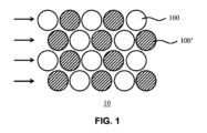
図1は、一実施態様による超音波トランスジューサアレイ10の上面図を概略的に示す。超音波トランスジューサアレイ10は、第1グループのCMUTセル100及び第2グループのCMUTセル100’に分割される複数のCMUTセルを有し、この場合、これらCMUTセルは限定することのない例のみとして円形形状を有するものとして示されている。CMUTセル100,100’に関しては他の形状も考えられる。セル100,100’は個別にアドレス指定されるように配置することができるが、好ましくは、各群のセルが一体的に(即ち、1つのトランスジューサ素子として)アドレス指定されるものとし、1つの群は両セル100,100’(好ましくは、等しい数のセル100,100’)を有して、各トランスジューサ素子が同じ広帯域特性を示すようにする(後に更に詳細に説明する)。超音波トランスジューサアレイ10は、このようなトランスジューサ素子のアレイとすることができる。CMUTセル100,100’は、当該超音波トランスジューサアレイ10のセル密度を増加させるために、図1に示されるように千鳥状に配置することができる。単一の行におけるセル100,100’を、水平矢印により示されるように、群化することができる(例えば、単一の行アドレス信号によりアドレス指定することができる)。図2は、第1グループのCMUTセル100及び第2グループのCMUTセル100’の各々の断面を概略的に示している。各CMUTセルは、基板101により支持された第1電極110と、該第1電極110に対向すると共に該第1電極から空洞(キャビティ)105により隔てられた第2電極120とを有している。
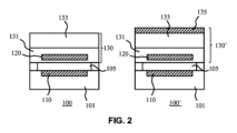
FIG. 1 schematically illustrates a top view of an
第1グループのCMUTセル100において、第2電極120は第1積層部130を有する可撓膜により支持され、該積層部は例えば酸化シリコン、窒化シリコン等の電気的に絶縁性の又は誘電体の材料の第1層131及び第2層133を含む。幾つかの応用例(例えば、低周波数応用例)において、第1積層部130は1ミクロンを遙かに超える厚さ(例えば、5~20ミクロンの厚さ)を有し得る。幾つかの他の応用例(例えば、高周波数応用例)において、第1積層部130は2ミクロン未満の厚さを有し得る。第2電極120は第1積層部130を有する可撓膜内に埋め込むことができ、かくして、例えば超音波トランスジューサアレイ10のCMUTセル100,100’の圧潰モードにおける動作の間において前記可撓膜の中央領域が基板101に接触する際に、第1電極110と第2電極120との間の短絡を防止するために第2電極120が空洞105から誘電体材料の薄い層により隔てられるようにする。
In the first group of
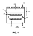
第2グループのCMUTセル100’において、第2電極120は第2積層部130’を有する可撓膜により支持され、該積層部は第1積層部130における層の何れよりも高い密度を有する材料の層135を含む。該質量層135は膜状積層部130’の曲げ剛性に大きな影響を与えることなく該膜状積層部130’の質量を増加させるために第2グループのCMUTセル100’の膜状積層部130’内に存在するものである。上記曲げ剛性は、特にCMUTセル100,100’が当該膜体の中央部分が基板101上に永久的に倒れ込む一方、該膜体における該中央部分の周囲の周辺部分が当該超音波トランスジューサ10の送信モードにおいて所望の周波数スペクトルを持つ超音波パルスを発生するように振動するか又は当該超音波トランスジューサ10の受信モードにおいて受信される所望の周波数スペクトルを持つパルスエコーに応答して共振する圧潰モードにおいて動作される場合に当該CMUTセル100,100’のバネ定数を主に定めることになる。このような圧潰モード動作自体は良く知られているので、簡略化のために、これ以上は詳細に説明しない。
In the second group of
円形のCMUTセル膜体の中心周波数Fcは、以下の式(1)により近似することができる:

膜体の曲げ剛性Dは、当該膜状積層部の有効ヤング率Eeffにより表すことができる:


一実施態様において、第1積層部130及び第2積層部130’の各層組成は、第1グループのCMUTセル100の膜体が第1バネ定数(有効ヤング率)を有する一方、第2グループのCMUTセル100’の膜体が上記第1バネ定数から20%以下だけ相違する第2バネ定数(有効ヤング率)を有するように選択される。より好ましくは、第2グループのCMUTセル100’の膜体は、前記第1バネ定数から10%以下だけ相違する第2バネ定数を有する。幾つかの実施態様において、第1バネ定数及び第2バネ定数は、略同一、即ち互いに1%未満しか相違しない。このことは、トランスジューサアレイ10のトランスジューサ素子がCMUTセル100及び100’の群により形成され、これらトランスジューサ素子が典型的に単一の制御信号(例えば、当該トランスジューサ素子の各CMUTセルを圧潰モードに付勢するための単一のバイアス電圧)によりアドレス指定される場合に特に有利である。というのは、CMUTセル100及び100’の同等のバネ定数は、当該トランスジューサ素子の動作の間において(例えば、超音波トランスジューサアレイ10の送信モード又は受信モードにおいて)該トランスジューサ素子の全てのセルが基板101上に倒れ込んだ状態に留まり得る(即ち、同等の動的“圧潰”挙動を呈し得る)ことを保証するからである。
In one embodiment, the layer composition of each of the
質量層135として、任意の好適な“重い”材料が、即ち、少なくとも7g/cm3の密度、好ましくは少なくとも10g/cm3の密度、更に好ましくは少なくとも15g/cm3の密度等の相対的に高い密度を持つ材料を用いることができる。当該質量層は、更に、好ましくは200GPa未満のヤング率を有する。100GPa未満のヤング率を持つ密な材料が特に好ましい。ヤング率は、例えばISO14577又はASTM E2546-07によるナノインデンテーション法を用いて(例えば、常温により)決定することができる。当該材料は、素材料又は複合若しくは合金材料とすることができる。該材料は、例えば、高い密度及び低いヤング率持つ金属(又は金属合金)、例えば金又はプラチナとすることができ、金が特に好適であると考えられる。それにも拘わらず、疑義を回避するために、質量層135は必ずしも金属又は金属合金である必要なないことが繰り返し述べられる。即ち、適切に高い密度及び低いヤング率を持つ如何なる好適な材料の使用も、考えることができる。
As the
図2に示されるように、第2積層部130’は、第1積層部130と同一とすることができるが、質量層135を更に含む。このような構成において、第2積層部130’のバネ定数は、該追加の質量層135の存在により、第1積層部130のバネ定数から僅かな量だけ相違するであろう。この理由により、質量層135の厚さは、第2積層部130’の曲げ剛性(即ち、バネ定数)に対する影響を最少にするために、好ましくは可能な限り小さく維持されるものとする。
As shown in FIG. 2, the
しかしながら、第1積層部130の層構成は第2積層部130’の層構成と相当に異なることができると理解されるべきである。例えば、第1積層部130は第2積層部13’における対応する層とは異なる厚さを持つ誘電体材料の1以上の層を有することができ、及び/又は第1積層部130は第2積層部130’には存在しない誘電体材料の1以上の層を有することができ若しくはその逆とすることができる。このことは、一層複雑な製造工程を必要とし得るが、このようにすることにより、第1積層部130及び質量層135を含む第2積層部130’の各曲げ剛性(即ち、バネ定数)を、最小限の差しか有ないように(例えば、(略)同一となるように)調整することができる。簡単な例として、第1積層部130は第1の厚さの誘電体材料の層を有することができる一方、第2積層部は上記第1の厚さより小さな第2の厚さの同じ誘電体材料の層を有することができ、ここで、第2の厚さは、該第2の厚さの誘電体材料の層及び質量層135の組み合わせが第1積層部130における第1の厚さの誘電体材料の層の曲げ剛性と(略)同一の曲げ剛性を示すように選定することができる。
However, it should be understood that the layer configuration of the
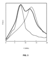
図3は、全てが質量層無しで同一の膜体を有するCMUTセル100の超音波トランスジューサアレイのFEM計算された周波数応答(点線)、全てが該膜体を有し、これら膜体上に1.5ミクロン厚の金層からなる質量層135が形成されたCMUTセル100’の超音波トランスジューサアレイの周波数応答(細い実線)及び斯様なCMUTセル100及びCMUTセル100’の交互のパターンを有する超音波トランスジューサアレイの周波数応答(太い実線)を示す。該周波数応答は、各トランスジューサアレイをDCバイアス電圧により圧潰モードで駆動すると共に各トランスジューサアレイの圧潰状態CMUTセルにAC刺激を印加することにより得られた。
FIG. 3 shows the FEM-calculated frequency response (dotted line) of an ultrasonic transducer array of
図3から分かるように、質量層135の追加は、CMUTセル100のピーク共振周波数を、約13MHzから質量層135を含むCMUTセル100’の約7MHzへとシフトさせる。太い実線により識別される単一の超音波トランスジューサアレイにおけるCMUTセル100及びCMUTセル100’の組み合わせは、CMUTセル100又はCMUTセル100’のみを有する超音波トランスジューサアレイと比較して略倍化された帯域幅を持つ周波数応答を示す。このことは、第1グループのCMUTセル100及び第2グループのCMUTセル100’の単一のトランスジューサアレイ10内の存在が該アレイの広帯域特性を改善することを明らかに示している。更に、このような複数グループのセルの単一トランスジューサアレイ10内での配置は、斯様なアレイの周波数応答を整形するために用いることもできることに注意すべきである。例えば、周波数応答を、該周波数応答において低い点(例えば、-3dB)に向かって非対称なプロファイルを有するように整形することができる。このような非対称なプロファイルは、例えば、当該アレイの第1高調波周波数において一層調和した波形を促すことができる。
As can be seen in FIG. 3, the addition of
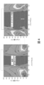
図4は、第1グループのCMUTセル100のみを有するトランスジューサアレイ10の出力圧の等高線プロット(左枠)及び各膜体に質量層135を含む第2グループのCMUTセル100’のみを有するトランスジューサアレイ10の出力圧の等高線プロット(右枠)である。水平軸は印加されるバイアス電圧[V]を示す一方、垂直軸は発生されたパルス長[ns]を示す。両等高線プロットを通して水平に延びる下側の点線は第1グループのCMUTセル100の中心周波数を示す一方、両等高線プロットを通して水平に延びる上側の点線は第2グループのCMUTセル100’の中心周波数を示す。ブロック矢印により示されているように、このようなCMUTセルの中心周波数は斯かるセルに質量層135を含めることにより一層低い値に実効的にシフトされ得、これによれば、超音波トランスジューサアレイ10の広帯域特性は当該アレイ内に複数グループのCMUTセルを含める(この場合、これらグループのうちの幾つかのみが斯様な質量層135を含む膜体を有する)ことにより増加することができることを示している。
FIG. 4 is a contour plot (left panel) of the output pressure of a
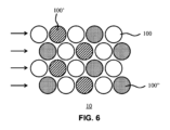
図5はCMUTセル100’の他の実施態様の断面を示すもので、該実施態様において質量層135はパターン化された層である。この構成は、例えば、第2グループのCMUTセル100’が該CMUTセル100’の各膜体が第1質量の質量層135を有する第1副グループ及び該CMUTセル100’の各膜体が第1質量より小さな第2質量の質量層135を有する第2副グループに分割されねばならない場合に有利であり得る。このような異なる質量を達成するために異なる厚さの質量層135を配置しなければならないというより、各質量層135は単一の厚さに形成することができ、第2副グループのCMUTセル100’の質量層135は、これら層の質量を減少させるためにパターン化される。当業者により即座に明らかとなるように、該パターンの密度及び/又は形状は、第2副グループのCMUTセル100’の質量層135の質量の減少を調整するために制御することができる。斯かるパターン化された層は、幾つかの実施態様では、同心リングのパターン又は当該膜体の上面の中心から放射状に延びる輻(スポーク)若しくは細条とすることができる。当業者により容易に理解されるように、当該膜体に所望の応力プロファイルを付与するために特定のパターンを選択することができる。
FIG. 5 shows a cross-section of another embodiment of CMUT cell 100', in which
このようにして、異なる質量の質量層135を含む複数グループのCMUTセルが存在する超音波トランスジューサアレイ10を形成することができる。図6は、このような超音波トランスジューサアレイ10の例示的実施態様を概略的に示すもので、該アレイは自身の各膜体に質量層を持たない第1グループのCMUTセル100、自身の各膜体に連続した質量層135を含む第2グループのCMUTセル100’及び自身の各膜体にパターン化された質量層135を含む第3グループのCMUTセル100”を有する。異なる中心周波数を持つ複数グループのCMUTセルを含めることは、当該超音波トランスジューサアレイ10の所望の周波数特性(例えば、広帯域特性)の精細な調整を可能にする。当業者によれば、図6の例示的超音波トランスジューサアレイ10は異なる質量の質量エレメントを含む2つの異なるグループのCMUTセルを有するが、このような超音波トランスジューサアレイが異なる質量の質量エレメントを含む3以上のグループ、例えば3つのグループ、4つのグループ及び5つのグループ等のCMUTセルを有することも等しく可能であることが即座に明らかとなるであろう。
In this way, an
図7に概略的に図示された代替実施態様において、第1グループのCMUTセル100及び第2グループのCMUTセル100’は異なる直径を有している。CMUTセル100及び100’の対が、単位セル(トランスジューサ素子)50を形成し得る。単位セル50内には(例えば、CMUTセル100,100’の間には)、これらCMUTセルを基礎となる基板内の回路(ASIC等)に接続するために相互接続部102が存在し得る。この実施態様において、単一グループ内のCMUTセル間のピッチは、当該超音波トランスジューサアレイ10の該トランスジューサの表面にわたる周波数特性が実質的に均一となることを保証するために、好ましくは一定とする。異なる直径を持つCMUTセルのグループを使用することは、選択されたグループ(又は複数のグループ)のCMUTセルに質量層135を追加する際の更なる設計自由度を提供する。このことは、圧潰モードの間においてCMUTセルの中心周波数は膜体半径から大いに独立したものとなるという事実を補償するために用いることができる。このことは、式(1)から理解することができ、この場合において、小半径膜体の圧潰半径Rcは大半径膜体のものより大幅に小さく、かくして、式(1)において項(1-x2)は項R2を補い、従って、CMUTセルが圧潰モードで動作される場合において中心周波数は膜半径に対して大いに不感的となる。
In an alternative embodiment schematically illustrated in FIG. 7, the
図8は、CMUTトランスジューサアレイ製造方法の限定するものでない例示的実施態様を概略的に示している。該方法はステップ(a)において基板101の準備を開始し、該基板はシリコン基板、シリコンオンインシュレータ基板、シリコンゲルマニウム基板及び窒化ガリウム基板等の任意の好適な基板とすることができる。シリコンベースの基板は、例えば、CMOS製造工程において用いることができる。基板101は、半導体装置、半導体装置及び/又はCMUTセルを相互接続する金属化積層部、金属化積層部上のパシベーション(不動態化)積層部等の幾つかの構造を有することができる。基板101は、例えば、自身の積層部(例えば、パシベーション及び/又は平坦化積層部)上に存在するならCMUTセル100、100’及び100”を含む特定用途向け集積回路(ASIC)の基板とすることができ、その場合、CMUTセルは基板101上の信号処理回路に金属化積層部により接続することができる。このような基板101を設けることは、それ自体良く知られており、当業者の常套的技術に属するものであるので、適切な基板101を設けることは簡略化のため更に詳細には説明しない。
FIG. 8 schematically illustrates a non-limiting exemplary embodiment of a CMUT transducer array manufacturing method. The method begins in step (a) with the provision of a
基板101上に第1電極110が形成され、該電極は、例えば金属又は金属合金、ドーピングされたポリシリコン等のドーピングされた半導体材料、(半)導電性酸化物等の任意の好適な導電材料から形成することができる。例えば、一般的に好まれる製造技術において容易に入手可能な金属を使用することが特に有利である。このことは、製造の流れの最小限の再設計しか必要とせず、これは費用の観点から魅力的であるからである。例えば、CMOS製造工程において、Al、W、Cu、Ti及びTiN等の導電材料並びに斯様な材料の組み合わせを、第1電極110を形成するために使用することができる。
A
第1電極110の形成は、基板101上の第1電極配置の形成の一部を形成することができ、該第1電極配置はCMUTセル100,100’,100”の各第1電極110を含む。
The formation of the
第1電極110及び基板101は、次いで、オプションとして電気絶縁(誘電体)材料層111により被覆することができる。これが、ステップ(b)に示されている。このような誘電体層111は、例えば、該第1電極110を対向電極120(下記参照)から電気的に絶縁し、当該CMUTセルの動作の間における斯かる電極の間の短絡の危険性を低減するために用いることができる。更に、誘電体層111は、第1電極110上に空洞を形成するための犠牲材料の除去の間において該第1電極110及び基板101を損傷から保護するために用いることができる。
The
誘電体層111は基板101の表面全体を覆うように示されているが、基板101の特定の部分のみが第1電極110と一緒に誘電体層111により被覆されるようなパターン化された誘電体層111を設けることも等しく可能である。第1電極110及び基板101の保護のために、例えば窒化シリコン(Si3N4)、酸化シリコン(SiO2)、酸化アルミニウム(Al2O3)又は酸化ハフニウム(HfO2)等から選択される1以上の材料等の任意の好適な誘電体材料を用いることができる。もっとも、好適な誘電体材料は、これらの例示的材料に限定されるものではないことを強調しておく。更に、上述した誘電体材料の混合物又は積層体も、第1電極110の保護のために用いることができる。このような誘電体層111は、例えばALD、(PE)ALD、PLD、PVD、LPCVD及びPECVD等の適切な堆積技術を用いる任意の好適な方法で形成することができるので、該層の形成は簡略化のために更に詳細には説明しない。
Although the
ステップ(c)において、第1電極110及びオプションとしての誘電体層111を含む基板101上に、例えば適切な堆積技術により犠牲材料が形成される。該犠牲材料は、第1電極110上の空洞が形成される第1領域112を含むと共に、当該犠牲材料を除去することができる通路(チャンネル)として働く、目的とされる空洞の外側の第2領域112’を更に有することができるようにパターン化される。形成されるべき空洞のギャップ高に対応する該犠牲材料層の高さは、典型的に、100~1,000nmの範囲である。もっとも、この範囲外の値も想定することができると理解されるべきである。
In step (c), a sacrificial material is formed on the
一実施態様において、第1領域112は、該第1領域112から1以上の歯状突起(例えば、2~8の斯様な突起)の形態で延びる第2領域112’を備えた円形領域である。このような犠牲材料層の上面図がステップ(c’)に示され、該図には4つの斯様な突起が限定するものでない例としてのみ示されている。該歯状第2領域112’は、典型的に、形成されるべき膜体の外側の空洞アクセスプラットフォームとして使用されるもので、該空洞アクセスプラットフォームを介して空洞を開成又は開放するための第1部分112へのアクセスを提供することができる。
In one embodiment, the
原理的に、如何なる好適な犠牲材料も用いることができるが、装置性能の理由で、後続のエッチング工程において効果的に除去することが可能な犠牲材料を用いることが好ましい。例えば、Al、Cr及びMo、Ti及び(Ti)W等の金属又はアモルファスシリコン又は酸化シリコン等の非金属の使用を考えることができる。Al、アモルファスシリコン及び酸化シリコン等の材料は、例えばCMOS製造工程において容易に利用可能であり、これらの材料のうちのAlはエッチングにより特に効果的に除去することができる。パターン化される犠牲材料は、例えば適切な堆積及びパターニング技術を用いる等の任意の好適な方法により形成することができるもので、その形成は簡略化のために更に詳細には説明しない。 In principle, any suitable sacrificial material can be used, but for device performance reasons it is preferred to use sacrificial materials that can be effectively removed in subsequent etching steps. For example, the use of metals such as Al, Cr and Mo, Ti and (Ti)W or non-metals such as amorphous silicon or silicon oxide can be considered. Materials such as Al, amorphous silicon and silicon oxide are readily available, for example in CMOS manufacturing processes, and among these materials Al can be removed particularly effectively by etching. The patterned sacrificial material may be formed by any suitable method, such as using suitable deposition and patterning techniques, and its formation is not described in further detail for the sake of brevity.
第1領域112の直径が、形成されるべきCMUT100,100’,100”の空洞の直径を定めることが理解されるであろう。一実施態様において、当該直径は20~500ミクロンの範囲に、より好ましくは50~300ミクロンの範囲に選択されるが、より大きな直径、例えば1,000ミクロンまでもの直径も想定され得ると理解されるべきである。
It will be appreciated that the diameter of the
ステップ(d)において、形成されるべき膜体の第1誘電体層131が、犠牲材料の第1領域112及び第2領域並びに、もし存在するなら、誘電体層111の露出部分上に堆積される。第1誘電体層131及び誘電体層111は犠牲層を除去するために共にエッチ法に曝されるので、第1誘電体層131及び誘電体層111は同一の材料のものとすることができるが、第1誘電体層131及び誘電体層111のために異なる材料を各々使用することも、勿論、もっともである。一実施態様において、第1誘電体層131及び誘電体層111は、各々、酸化シリコン層(例えば、SiO2)、窒化シリコン層(例えば、Si3N4等)、酸化アルミニウム(Al2O3)層及び酸化ハフニウム(HfO2)層等の何らかの好適な誘電材料から形成された少なくとも1つの層を有する。当業者にとり、多くの他の好適な誘電体層材料が明らかであろう。好ましくは、斯かる誘電体層を形成するためにPECVD及びALD等の堆積技術が用いられる。これらの技術は400℃より低い温度で実行することができ、このことは、これら技術をCMOS製造処理と両立させ得るからである。第1誘電体層131は積層体、例えば酸化物-窒化物積層体又は酸化物-窒化物-酸化物積層体として形成することができる。同様に、オプションとしての誘電体層111も斯様な積層体として形成することができる。オプションとしての誘電体層111及び第1誘電体層131のために任意の好適な誘電体材料を用いることができることを繰り返し言及する。更に、これらの誘電体層のために、上述した誘電体材料の混合物又は積層(例えば、ALD積層)を用いることもできる。
In step (d), a first
第1誘電体層131の形成の後、第2電極120を含む第2電極配置が、ステップ(e)に示されるように第1誘電体層131上に各第2電極120が第1電極110に対向されるようにして形成される。該第2電極配置は、好ましくは、前記第1電極配置のものと同一の導電材料から形成されるものとするが、第2電極配置及び第1電極配置は他の例として異なる材料から形成することもできると理解されるべきである。第2電極配置は、例えば、Al、W、Cu、Ti及びTiN等並びに斯かる材料の組み合わせのような任意の適切な導電材料から形成することができる。第2電極配置は良く知られた技術を用いて形成することができるが、これら技術は簡略化のために更に説明されることはない。第1電極110を含む第1電極配置及び第2電極120を含む第2電極配置は、例えば50~250nm厚等の任意の適切な厚さに形成することができる。例えば応用分野に依存して、他の好適な厚さも考えられる。
After formation of the
第2電極120の形成の後、本方法は第2誘電体層133が形成されるステップ(f)に示されるように進む。オプション的な実施態様において、第2誘電体層133は第1電極110と第2電極120との間における犠牲材料の第1部分112の厚さを超える第1厚さt1に形成され、かくして、空洞105を形成した際に空洞ギャップの高さgが該厚さt1より大幅に小さくなる(即ち、g/t1≪1)ようにする。好ましくはt1≧3g、より好ましくはt1≧5gとする。このことは、ステップ(g)における空洞105の解放(即ち、アクセス部又はビア116の形成及び後続する犠牲材料の第1部分112及び第2部分112’の除去による)の間において、該空洞105を形成するための犠牲材料の除去の段階においてg≪t1となるので、当該膜体が該空洞解放の間において優れた膜強度を示すことを保証する。更に、第2誘電体層133は空洞105の解放の前に形成(例えば、堆積)されるので、優れた平坦特性を持つ膜体が得られる。該第2誘電体層133の形成の間において犠牲材料の存在が第1誘電体層131の変形を防止するからである。
After forming the
犠牲材料の第1部分112及び第2部分112’は、次いで、ステップ(g)に示されるようにCMUTセル100,100’の第1電極110と、膜状積層部130における第1誘電体層131と第2誘電体層133との間に埋め込まれた第2電極120との間に空洞105を形成するために適切なエッチ法を用いてアクセス部又はビア116を形成することにより除去される。このような通常の犠牲材料のための好適なエッチ法自体は良く知られており、当業者であれば自身の通常の知識を用いて適切なエッチ法を選択することは困難ではないであろう。
The
積層部130の厚さは、ステップ(h)におけるアクセス部又はビア116の密閉の間において該アクセス部又はビア116内の栓118を含む更なる誘電体層134の形成により更に増加され得る。該更なる誘電体層134は、第2誘電体層133より大幅に薄くすることができる。該更なる誘電体層134は、上記アクセス部又はビア116を効果的に密閉するために空洞105の高さの少なくなくとも2倍(例えば、該高さの3~4倍)の厚さに形成することができる。
The thickness of
ステップ(i)において、第2グループのCMUT素子100’の膜状積層部130’を形成するために、選択された膜状積層部130に質量層135が被着される。このような質量層135は、例えば膜状積層部130にわたってマスク層を被着し、質量層135が被着される膜状積層部130を露出させるために該マスク層をパターニングする(質量層の被着後、該マスク層は除去することができる)ことによる等の任意の適切なやり方で選択的に被着することができる。質量層135を選択的に被着させるための他の好適な技術は、当業者にとり即座に明らかになるであろう。明示されていないが、第2グループのCMUTセル100’における更なる差別化は、選択された質量層135をパターニングして、前述したような異なる質量の質量層135を有する第1副グループ及び第2副グループのCMUTセルを形成することにより達成することができる。
In step (i), a
この時点で、ステップ(a)~(i)は、1以上のCMUTセル100、100’及び100”( 基板101上に存在する場合)を形成する有利であるが限定するものでない例を概略的に示すものであることが強調される。当業者によれば、多数の他の方法が明らかであろう。
At this point, steps (a)-(i) schematically illustrate an advantageous but non-limiting example of forming one or
注目すべき製造工程変形例は、前記アクセス部又はビア116を、例えば栓118を形成するために金属又は誘電体層等の専用の密閉層を堆積及びパターニングすることによる等の何らかの好適な材料を用いる任意の好適なやり方で密閉することができるというものである。更に、前記空洞105は、例えば第2誘電体層133の形成前等の当該CMUT製造工程における任意の好適な時点で解放することができることが注記される。他の注目すべき製造工程変更例は、第1電極110及び/又は第2電極120を誘電体層により空洞105から分離することができ又は分離しなくてもよいというものである(これは、典型的な設計上の選択であるからである)。前述したように、当該CMUTセル100、100’及び100”(存在する場合)の動作の間において第1電極110と第2電極120との間の直接的接触を防止するために第1電極110及び/又は第2電極120上に誘電体層(即ち、電気絶縁層)を設けることができる。
A notable manufacturing process variation is to form the access or via 116 with any suitable material, such as by depositing and patterning a dedicated sealing layer, such as a metal or dielectric layer, to form the
膜状積層部130は、例えば誘電体層の積層体というより単一の誘電体層等による等の、任意の好適な態様で形成することができる。このような製造工程上の選択は当業者の常套的技量内に入るもので、明示的には言及しない。前述したように、全てのCMUTセル100,100’が同一の膜状積層部130を有し得るものではない。第2グループのCMUTセル100’における質量層135の存在に加えて、積層部130及び130’の間で異なる層及び/又は異なる層厚を有することも等しく可能である。
The
また、個々のCMUTセル100の他の設計も勿論可能であると理解されるべきである。CMUTセル100の設計は本発明に特に関連があるものではなく、これらセルの任意の好適な設計が想定され得る。例えば、底部電極110と空洞105との間に中間電極が配置されるような3電極CMUTセル100も等しく可能である。このような3電極CMUTセルは、例えば、刺激及びバイアス電圧を別個の電極を介して供給するために(CMUTセルの底部へ膜体が固着する危険性を低減するために)想定することができる。
It should also be understood that other designs of
この時点で、種々の実施態様には図示されていないが、実施態様に従って製造されるCMUTセル100、100’及び100”(存在する場合)は、更なる回路エレメントを有することができ、これら回路エレメントは基板101上に集積することができるか、又は別の基板上に設けられると共に本発明の実施態様に従って製造されるウェファからのCMUT装置の1以上と一緒に単一のパッケージに統合することができると理解されるべきであることを更に注記する。このような更なる回路は、例えば、1以上のCMUTセル100、100’及び100”(存在するなら)を制御し及び/又は1以上のCMUTセル100、100’及び100”(存在するなら)により発生される信号を処理する(例えば、該1以上のCMUTセル100、100’及び100”(存在するなら)の送信及び/又は受信モードを制御するために)ためのIC(例えば、ASIC)とすることができる。CMUTセル100、100’及び100”(存在するなら)及び/又は斯様なセルを有する超音波トランスジューサアレイの他の好適な実施態様は、当業者によれば即座に明らかとなるであろう。
At this point, although not shown in the various embodiments, the
更に、上述した製造工程において、該製造工程の間において処理されるウェファは、単一のダイ、即ち単一の装置を含むことができ(この場合、基板101が該ウェファに対応する)、又は当該装置製造工程の完了の後に何らかの適切な方法で単一化する(例えば、ダイシングする)ことができる複数のダイを含むことができる(この場合、基板101は当該ウェファの一部に対応し、その例示的実施態様は後に更に詳細に説明される)ことが注記される。
Further, in the manufacturing process described above, a wafer processed during the manufacturing process may comprise a single die, i.e. a single device (in which
図9は、一実施態様による前述した複数グループの円形CMUT素子50(これらの各々は、前述したようなCMUTセル100、100’及び100”(存在するなら)を含み得る)の二次元トランスジューサアレイ10の平面図である。該アレイは、従来の態様で対称に整列されたCMUT素子の行56及び列58に構成されている。この例において、各列58は埋め込まれた金属トラックを含む一体の可撓箔により被覆され、このことは、これら列が円筒状に曲げられることを可能にする。該可撓箔は後に詳細に説明する。この例において、当該アレイは、列方向におけるピッチを示す矢印52及び行方向におけるピッチを示す矢印54により示されるように、行及び列の両方向において同一のピッチを有するように寸法決めされている。これら列58は別個の基板アイランド(例えば、別個のシリコンアイランド又は細条)として形成することができ、かくして、当該トランスジューサアレイ10は三次元主体(例えば、カテーテルの外部シース等の円筒状主体)の周囲に巻き付けることができる。
FIG. 9 illustrates a two-dimensional transducer array of groups of circular CMUT elements 50 (each of which may include
図10は、好ましい実施態様により構成された二次元超音波トランスジューサアレイ10の平面図である。図10に示されるように、CMUT素子50のグループの行56及び列58は、それ自体は良く知られているように、千鳥状に配列されている。この例における千鳥状配列はCMUT素子50間の間隔55を列方向に増加させることにより適合され、該増加は隣接する列及び行が更に一層互い同士で分散配置される(互いに更に間隔をつめられる)ことを可能にする。一実施態様において、間隔55は少なくともCMUT素子50の直径である。複数グループのCMUTセル100、100’(及び100”等)を備えたトランスジューサ素子50を有するトランスジューサアレイ10において、同一のグループのCMUTセル100,100’の間のピッチは、好ましくは、当該アレイにおいて一定であるものとし、かくして、当該アレイが該アレイの全トランスジューサ面積にわたって均一な広帯域特性を示すようにする。
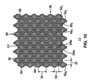
FIG. 10 is a plan view of a two-dimensional
図示された例において、トランスジューサ素子50は、セルからセルへの列又は行方向の接線が隣接する千鳥配置された列又は行のセルと実際に交差するほど密に間隔がつめられている。トランスジューサ素子50の該間隔詰めは、トランスジューサ素子50の間の垂直方向の(即ち、列方向の)間隔の増加を要せずに、少なくともトランスジューサ素子50の最も密な充填が達成される点までの当該トランスジューサアレイ10内のCMUT素子の密度の増加を可能にする。この点を超えて、列方向における連続するCMUT素子50の間のピッチを矢印55が示すように増加して、矢印57及び59により示されるような水平方向の間隔の更なる低減を促進することができるが、このことは当該トランスジューサアレイの全体のCMUT密度を減少させる。図10のCMUTトランスジューサアレイ10は、少なくとも最密な充填において、図9のCMUTトランスジューサアレイ10よりも高いセル密度を有する。
In the illustrated example, the
図10において、CMUT素子50の各列58は、別個の基板アイランド、即ちシリコンダイの別個の断片上に配置されている。各基板アイランド(例えば、シリコンアイランド)は、列58の長さ方向に(即ち、列58に沿って)蛇行するエッジ構造を有することを特徴とし、エッジ部58aはトランスジューサ素子50の周囲で外側方向に蛇行する一方、エッジ部58bは1つの列58における隣接するCMUTセル50,50’の間の間隔へと内側方向に蛇行する。言い換えると、列58は列方向に波状の対向するエッジを有し、これら波のピークはCMUTセル50,50’に一致し、波の谷はCMUT素子50の間の空間55に一致する。
In FIG. 10, each
隣接する列58は、自身のシリコンアイランドの外側方向に蛇行するエッジ部が隣接するシリコンアイランドの内側方向に蛇行するエッジ部と整列する(即ち、内側方向に蛇行するエッジに入り込む)ように配置され、これにより、隣接する列58の間のCMUT素子50の千鳥状整列によりCMUT素子50の千鳥状の行を形成する。隣同士のシリコンアイランドは、典型的に、ギャップ57により分離され、例えば当該CMUTトランスジューサアレイ10を円筒状主体(例えば、カテーテルのシース)等の三次元主体の周りに巻き付ける場合に斯かるシリコンアイランドの互いに対する面外への曲げを容易にする。
上記基板アイランドの互いに対する相対位置を維持するために、CMUTトランスジューサアレイ10は該基板アイランドが取り付けられる可撓箔60を更に有する。該可撓箔60は、例えば、金属層又は金属積層体(例えば、金属トラック)がポリマ層又はポリマ積層体に埋め込まれ(又は、により被覆され)、該ポリマが典型的に上記金属層を偶発的短絡から保護するために電気的に絶縁するような所謂フレックス・リジッド(可撓/剛性)箔を有することができる。このような可撓箔60のための好適なポリマの限定するものでない例は、ポリイミドである。ポリイミドはCMOS製造工程等の多くの半導体製造工程と相性が良いことが良く知られているからである。当業者によれば、例えばパリレン等の他の好適なポリマも即座に明らかとなるであろう。好適な金属の限定するものでない例は、アルミニウム又は半導体製造工程において一般的に使用される何らかの他の金属である。このような材料の既存の半導体製造工程との相性は、製造方法を再設計又は再開発しなければならない(このことは、CMUTトランスジューサアレイ10のコストを増加させ得る)というより、既存の半導体製造工程を用いて当該CMUTトランスジューサアレイの製造を容易化する。
In order to maintain the relative positions of the substrate islands with respect to each other,
可撓箔60を介して相互接続された複数の隣接する蛇行基板アイランド上にCMUT素子50を設けることは、当該CMUTトランスジューサアレイ10の該アレイの行方向における面外の曲げを可能にすると同時に該アレイの列方向における構造的完全性を提供し、このことは、例えば該アレイを血管内カテーテル又は心臓内カテーテル等のカテーテルの周りに巻き付ける場合に特に有利である。例えば、当該CMUTトランスジューサアレイ10は、このようなカテーテルの外部シースの周りに前記シリコンアイランド列58を該カテーテルの長さ方向に整列させて巻き付けることができる(即ち、CMUTトランスジューサアレイ10は面外に曲げられ、該カテーテルシースの周りに行方向に巻き付けられる)。多数の相対的に狭いシリコンアイランドを設けることにより、CMUTトランスジューサアレイ10をカテーテルシース等の円筒状主体の周りに巻き付ける場合に該CMUTトランスジューサアレイ10の略円筒状の構造を実現することができ、斯様なCMUTトランスジューサアレイが斯かる主体の全表面にわたり連続的となる(例えば、文献EP2455133A1の場合におけるように、CMUTトランスジューサアレイの一部を形成する隣接する長方形シリコンアイランドの間の不連続部を含まない)という更なる利点を伴う。
Providing
本発明の他の態様によれば、この減少された間隔57及び59の利点が、図10のアレイをトランスジューサ素子50の動作行が素子の水平の行56ではなく、2つの(又はそれ以上の)隣接する千鳥配列された行の間隔のつめられた組み合わせとなるように動作させることにより利用される。このことは、素子の動作行が素子の完全に線状の行であるような従来のダイシングされた圧電トランスジューサ素子の知識とは反するものである。図10の例において、素子の動作行は素子の千鳥配列された行により形成される。例えば、図10における1つの動作行は、2つの隣接する千鳥配列された行のトランスジューサ素子621,622,623,624,…62Nを有する。即ち、M番目の動作行はCMUT素子50の各列58のM番目のCMUT素子50を有し、Mは正の整数であり、各行はカテーテルの周囲に巻き付けられた場合に蛇行する環状の行を形成する。千鳥配列された行の一層密な間隔は、96個のセルの動作行が設けられることを可能にし(ここで、標準的な対称配列は、例えば、64個のセルしか収容しない)、斯かる動作行の千鳥状構造は、アンテナパターンにおける減少されたグレーティングローブによる一層小さなクラッタにより高度に解像される画像のための音響信号を依然として供給することができる。このような千鳥配列された行は、例えば、隣接する列58の適切なCMUT素子50を順次駆動する(例えば、N個の列58のトランスジューサ素子621,622,623,624,…62Nを順次駆動する)ことによりアドレス指定することができる。
According to another aspect of the invention, the advantage of this reduced
図10の実施態様において、各基板(例えば、シリコン)アイランドは、連続した可撓箔60により保持されている。他の実施態様において、可撓箔60は、該可撓箔60が前記ギャップ57に整列した複数の凹部(recess)を有し、該可撓箔60の異なる領域(例えば、異なる基板(シリコン)アイランドを保持する異なる領域)を相互接続するために各ブリッジ部又はブリッジがギャップ57に跨がって延在するようにパターン化することができる。この構成は、当該CMUTトランスジューサアレイの可撓性を増加させるが、より低い強度のものとなり得る。
In the embodiment of FIG. 10, each substrate (eg silicon) island is held by a continuous
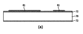
図11は、CMUT素子50が配置された2つのシリコンアイランドを結合する可撓箔ブリッジの形成における幾つかの製造方法ステップを示す。図11の(a)は、上面及び底面上に熱二酸化シリコン層72が成長されたシリコンウェファ70を示す。上面には、標準的リソグラフィを用いて、パターン形成されたアルミニウム領域81がスパッタリングされる。上面における該アルミニウム領域の一方上にポリイミドのパターン形成された領域74が設けられ、該パターンが当該可撓箔におけるブリッジを画定する。連続した可撓箔の場合、ポリイミド74は連続したシートであり得る。該ポリイミド74上にアルミニウム層80が堆積され、該アルミニウム上に第2のポリイミド層76が設けられる。図11の(b)に示されるように、エッチングの間においてマスクとして使用するために、他のアルミニウムの層82がアルミニウム層80上にパターン形成される。
FIG. 11 shows several manufacturing method steps in forming a flexible foil bridge that joins two silicon islands on which
最後に、図11の(c)に示されるように、シリコンウェファ70は、共にCMUT位置88の下及び可撓性ブリッジ74,80,76の下である、厚いレジストによりマスキングされた領域84の外側の領域において背後からエッチング除去される。上面における可撓性ブリッジ90の両側におけるポリイミド層76はエッチマスク層82の両側においてパターニング除去され、該エッチマスク層自体も次いでエッチング除去される。その結果は、可撓性ブリッジ90により結合された2つの別個のシリコンアイランド92及び94である。可撓性ブリッジ90及び該ブリッジに類似した他のものは、斯様なCMUTが植設されたアイランドのアレイが円筒形状に巻き付けられることを可能にし、心臓内カテーテルトランスジューサの要求に適合する。
Finally, as shown in FIG. 11(c), the
前述したように、音響トランスジューサ素子50の動作行200は、従来のように真っ直ぐな行のトランスジューサ素子により形成されるのではなく、CMUTセル50,50’の2以上の隣接する千鳥配列された行202及び204により形成される。図12は超音波トランスジューサアレイ10の代替実施態様を概略的に示すもので、該実施態様において、各シリコンアイランド列58は1対の千鳥状配列に配置されたCMUT素子50を有する列を有する。即ち、第1列における1つのCMUT素子50の領域は隣接する列における隣接するCMUT素子50の間の間隔へと延在し、かくして、これらの隣接するCMUTセルの間の接線が、好ましくは、これらの隣接するCMUT素子の間の間隔へと延在するCMUT素子50の領域と交差するようにする。
As previously mentioned, the
前述したものと同様に、シリコンアイランド列58は該列58の長さ方向において(即ち、該列58に沿って)蛇行するエッジを有し、CMUT素子50の周りで外側に向かって蛇行するエッジ部分及び列58における隣接するCMUT素子50の間の間隔へと内側に向かって蛇行するエッジ部分を備える。隣接する列58は、自身のシリコンアイランドの外側に向かって蛇行するエッジ部分が隣接するシリコンアイランドの内側に向かって蛇行するエッジ部分と整列する(即ち、該内側に向かって蛇行するエッジ部分に入り込む)ように構成され、これにより、隣接する列58の間のCMUT素子50の千鳥状整列によりCMUT素子50の千鳥配列された行を形成する。隣接するシリコンアイランドは、典型的に、例えば当該CMUTトランスジューサアレイ10を前述したようにカテーテルシースに巻き付ける場合におけるシリコンアイランドの互いに対する面外への曲げを容易にするためにギャップ57により分離される。
Similar to that previously described, the
この実施態様は、より大きな(即ち、より広い)シリコンアイランドをもたらし、このことが斯かるアイランドの構造的剛性を改善する一方、行方向に優れた可撓性を備えた超音波トランスジューサアレイを依然として提供するという利点を有する。この実施態様は、当該トランスジューサアレイが巻き付けられる主体(例えば、カテーテルシース)の周面が単一のシリコンアイランドの幅の何倍もあり、多数のシリコンアイランドが該主体に巻き付けられるべきものとなり、該主体の周りに実質的に連続したトランスジューサ行が設けられるようになる場合に、特に有利である。 This embodiment results in larger (i.e., wider) silicon islands, which improves the structural rigidity of such islands while still providing an ultrasound transducer array with excellent flexibility in the row direction. have the advantage of providing This embodiment is such that the circumference of the body (e.g., catheter sheath) around which the transducer array is wrapped is many times the width of a single island of silicon, such that multiple islands of silicon are to be wrapped around the body. It is particularly advantageous when a substantially continuous row of transducers is provided around the main body.
前述したのと同様に、動作行200の方向は面内ビームステアリング方向である。即ち、ビームステアリングは、典型的に、列58に対して垂直に行われる。別個のシリコンアイランドは、これらシリコンアイランドの各向きを維持すると共に、当該二次元トランスジューサアレイ10が図13に示されるようにカテーテル250の遠位先端210の周囲で円筒形状に曲げられることを可能にするために、可撓箔60(例えば、図に示されるような連続した箔又は隣接するシリコンアイランドの間のギャップを跨ぐブリッジ部90を含むパターニングされた箔)と重ね合わされる。当該アレイは限定するものでない例示としてのみ遠位先端210に巻き付けられていると理解されるべきである。即ち、アレイ10はカテーテル250の遠位先端の近くに配置されることが好ましいが、例えば該トランスジューサアレイ10をカテーテル250の任意の他の部分に巻き付けることも等しく可能である。幾つかの実施態様において、カテーテル250は、遠位先端210上に、例えば該巻き付けられた超音波トランスジューサアレイ10に加えて円形の周を持つ平面状超音波トランスジューサアレイ等の他の超音波トランスジューサアレイ(図示略)も有することができ、かくして、カテーテル250は該カテーテルの前方の及び該カテーテルの周囲の身体部分の画像を発生することができ、このことは、例えば心臓内撮像の際に特に有利である。幾つかの実施態様において、カテーテル250は、従って、心臓内カテーテル又は血管内カテーテルとすることができる。
As before, the direction of
図14及び図15は、本発明の他の実施態様による2つのCMUTアレイ10の平面図である。図14において、各CMUT素子50は自身の基板(例えば、シリコン)アイランド92上に作製されている(図11参照)。CMUT素子40の各列58は、可撓箔の細条60と重ねられ、隣接する列の箔細条は、図11に示された様に形成される可撓性ブリッジ90により相互接続されている。可撓箔細条60はアルミニウム等の導電材料を有することができ、該導電材料は当該列内の超音波素子を一緒にアドレス指定するか、又は斯かる素子を接地等の同一の電位に維持することができる。当該トランスジューサアレイ10内の素子50の個々のアドレス指定は、集積回路を介して実現することができる。上記可撓性ブリッジは、このようにして、当該トランスジューサアレイ10の素子50の向き維持することを助ける一方、該アレイが湾曲された構造に屈曲及び湾曲されることを可能にする。特に、この実施態様において、CMUTトランスジューサアレイ10は、各列58が可撓箔細条60におけるブリッジ構造90により相互接続された複数の基板アイランドにより形成されることにより、行方向及び列方向に曲げることができる。
14 and 15 are plan views of two
図15は、各基板(例えば、シリコン)アイランド92上に2つのCMUT素子50,50’が存在することを除き類似したCMUTアレイ10を示す。例えば、隣接する素子列のCMUT素子50及び50’は、共に同一のシリコンアイランド上に配置される。該2つの隣接する列は可撓箔細条60と重ねられ、隣接する箔細条は可撓性ブリッジ90により相互接続され、このことは、CMUTトランスジューサアレイ10の湾曲された又は円筒状の形状への曲げを可能にする。
FIG. 15 shows a
前述したのと同様に、ブリッジ構造90により相互接続された別個の部分を有する可撓箔細条60の代わりに、各基板アイランドを保持するために連続した可撓箔を用いることもできる。このような代替実施態様は、一層強固であるが、一層限られた可撓性しか有さないであろう。しかしながら、このことは、当該CMUTトランスジューサアレイ10が適合される主体の曲率が相対的に限られたものであるなら問題とはならないであろう。
As before, instead of flexible foil strips 60 having separate portions interconnected by
この時点で、図9~図15における実施態様はCMUTセル100,100’の群(クラスタ)を有するCMUT素子50に関して説明されたものであるが、各CMUT素子50が単一のCMUTセル(例えば、CMUTセル100又はCMUTセル100’)を有することも等しく可能であり、後者の場合、当該トランスジューサアレイ10は典型的にCMUT素子50としてCMUTセル100,100’の交互のパターンを有することが更に注記される。
At this point, although the embodiments in FIGS. 9-15 were described in terms of
図16は超音波診断撮像システム1の例示的実施態様をブロック図の形で概略的に示すもので、該システムは、一緒に接続されて単一のトランスジューサ素子として一体的に動作される複数のCMUTセル100及び/又は100’を有する超音波トランスジューサアレイ10(例えば、超音波トランスジューサ素子タイル(トランスジューサ素子)のアレイ)を備える。アレイ10は、前述したように、カテーテル250等の超音波プローブの一部を形成することができる。図16において、トランスジューサアレイ10は超音波を送信すると共にエコー情報を受信するために設けられる。前述したように、トランスジューサアレイ10は、2D面で又は3D撮像のために三次元でスキャンすることができる超音波トランスジューサ素子タイルの一次元又は二次元アレイとすることができる。
FIG. 16 schematically illustrates in block diagram form an exemplary embodiment of an ultrasonic
トランスジューサアレイ10は、プローブ又はカテーテル250に組み込むことができるマイクロビーム形成器12に結合することができ、該マイクロビーム形成器は超音波トランスジューサセル100(又は超音波トランスジューサセルのクラスタ)による信号の送信及び受信を制御する。マイクロビーム形成器は、例えば米国特許第5,997,479号(Savord他)、米国特許第6,013,032号(Savord)及び米国特許第6,623,432号(Powers他)に記載されているように、トランスジューサ素子タイルのグループ又は“パッチ”により受信される信号の少なくとも部分的ビーム形成を行うことができる。
The
マイクロビーム形成器12は送信器/受信器(T/R)スイッチ16を有する端末(例えば、患者インターフェースモジュール等)にプローブケーブル(例えば、同軸ワイヤ)により結合することができ、上記T/Rスイッチは送信モードと受信モードとの間を切り換えると共に、マイクロビーム形成器が存在しないか又は使用されず、トランスジューサアレイ10が主(システム)ビーム形成器20により直接的に動作される場合に該主ビーム形成器20を高エネルギ送信信号から保護する。マイクロビーム形成器12の制御の下でのトランスジューサアレイ10からの超音波ビームの送信は、T/Rスイッチ16により前記マイクロビーム形成器に結合されたトランスジューサコントローラ18及び主システムビーム形成器20により指示することができ、これらはユーザインターフェース又は制御パネル38のユーザ操作から入力を受信する。トランスジューサコントローラ18により制御される機能の1つは、ビームがステアリング及び収束される方向である。ビームは、トランスジューサアレイ10から真っ直ぐ前方に(垂直に)、又は一層広い視野のために異なる角度でステアリングすることができる。トランスジューサコントローラ18は、超音波トランスジューサアレイ10のための電圧源45を制御するように結合することができる。例えば、電源45は、それ自体良く知られているように、CMUT素子の1以上のCMUTセル100,100’を圧潰モードで動作させるためにCMUTアレイ10のCMUT素子に印加されるDC及びACバイアス電圧(又は複数の電圧)を設定する。
The
この目的のために、電源45は、オプションとして、上記DC及びAC又は例えば送信モードにおいてCMUTセル100の駆動電圧の各刺激成分を供給するための別個のステージを有することができる。第1ステージは静的(DC)電圧成分を発生するように構成することができる一方、第2ステージは設定された交流周波数を持つ交流可変電圧成分又は刺激を発生するように構成することができ、該信号は典型的に全体の駆動電圧と上述した該駆動電圧の静的成分との間の差分である。印加される駆動電圧の静的又はバイアス成分は、好ましくは、当該CMUT素子を圧潰状態にさせる場合の(即ち、これらCMUT素子を圧潰モードで動作させる場合の)閾電圧を満たす又は超えるものとする。この構成は、全体の電圧の特に低ノイズの静的成分を発生させるために第1ステージが相対的に大きなコンデンサ(例えば、平滑コンデンサ)を含むことができるという利点を有し、ここで、上記静的成分は典型的に上記全体の電圧を全体の電圧信号のノイズ特性が該静的成分のノイズ特性により支配されるように支配するものである。
To this end, the
電源45の他の好適な実施態様は、例えば、該電源45がCMUT駆動電圧の静的DC成分を発生するための第1ステージ、該駆動電圧の可変DC成分を発生するための第2ステージ、及び当該信号の周波数変調又は刺激成分を発生するための第3ステージ(例えば、パルス回路等)を含む3つの別個のステージを含む実施態様等のように、明らかであろう。
Other suitable embodiments of the
マイクロビーム形成器12により生成される部分的にビーム形成された信号は主ビーム形成器20に送ることができ、ここで、トランスジューサ素子の個々のパッチからの該部分的にビーム形成された信号は完全にビーム形成された信号へと組み合わされる。例えば、主ビーム形成器20は128のチャンネルを有することができ、これらチャンネルの各々が数十又は数百の超音波トランスジューサセル100,100’のパッチからの部分的にビーム形成された信号を受信する。このようにして、トランスジューサアレイ10の数百のトランスジューサ素子により受信された信号が、単一のビーム形成された信号に効率的に貢献することができる。
The partially beamformed signals produced by the
ビーム形成された信号は、信号プロセッサ22に結合される。信号プロセッサ22は受信されたエコー信号を帯域通過フィルタ処理、デシメーション、I及びQ成分分離及び高調波信号分離等の種々の方法で処理することができ、該処理は線形及び非線形信号を分離して、組織及びマイクロバブル(微少気泡)から戻る非線形(基本周波数の高い調波)エコー信号の識別を可能にするように働く。
The beamformed signals are coupled to signal
信号プロセッサ22は、オプションとして、スペックル(斑紋)低減、信号合成(signal compounding)及びノイズ除去等の付加的信号強調を実行することができる。信号プロセッサ22における上記帯域通過フィルタは、エコー信号が増加する深度から受信されるにつれて自身の通過帯域が高い周波数帯域から低い周波数帯域にシフトする追跡フィルタとすることができ、これにより、一層大きな深度からの一層高い周波数におけるノイズ(一層大きな深度では、これらの周波数は解剖学的情報に欠ける)を排除する。
上記の処理された信号は、Bモードプロセッサ26に、及びオプションとしてドプラプロセッサ28に供給することができる。Bモードプロセッサ26は、身体内の臓器及び血管の組織等の身体内の構造の撮像のために、受信された超音波信号の振幅の検出を採用する。身体の構造のBモード画像は、例えば、米国特許第6,283,919号(Roundhill他)及び米国特許第6,458,083号(Jago他)に記載されているように、高調波画像モード、基本画像モード又は両モードの組み合わせの何れかで形成することができる。
The above processed signals may be supplied to B-
ドプラプロセッサ28(存在するなら)は、画像フィールド内の血液細胞の流れ等の物質の動きを検出するために、組織運動及び血流からの時間的に区別できる信号を処理する。該ドプラプロセッサは、典型的に、身体内の選択されたタイプの物質から戻るエコーを通過及び/又は拒絶するように設定することができるパラメータを備えたウォールフィルタを含む。例えば、該ウォールフィルタは一層高い速度の物質からの相対的に低い振幅の信号を通過させる一方一層低い又はゼロ速度の物質からの相対的に強い信号を拒絶する帯域通過特性を有するように設定することができる。 A Doppler processor 28 (if present) processes the temporally distinct signals from tissue motion and blood flow to detect movement of materials such as blood cell flow within the image field. The Doppler processor typically includes a wall filter with parameters that can be set to pass and/or reject echoes returning from selected types of material within the body. For example, the wall filter is set to have a bandpass characteristic that passes relatively low amplitude signals from higher velocity material while rejecting relatively stronger signals from lower or zero velocity material. be able to.
この帯域通過特性は、流れる血液からの信号を通過させる一方、略静止した又は心臓の壁等の緩やかに移動する物体からの信号を拒絶する。逆の特性は、組織の動きを検出及び描写する組織ドプラ撮像と称されるもののために、心臓の運動する組織からの信号を通過させる一方、血流信号は拒絶する。当該ドプラプロセッサは、画像フィールド内の異なる点からの時間的に離散したエコー信号の系列を受信及び処理することができ、特定の点からの該エコーの系列はアンサンブルと称される。相対的に短い期間にわたり立て続けに受信されるエコーのアンサンブルは、流れる血液のドプラシフト周波数を推定するために使用することができ、該ドプラ周波数の速度に対する対応が血流速度を示す。より長い期間にわたり受信されるエコーのアンサンブルは、緩やかに流れる血液又は緩やかに動く組織の速度を推定するために使用される。 This bandpass characteristic allows signals from flowing blood to pass, while rejecting signals from substantially stationary or slowly moving objects such as the walls of the heart. The opposite property allows signals from moving tissue of the heart to pass, while rejecting blood flow signals, for what is referred to as tissue Doppler imaging, which detects and depicts tissue motion. The Doppler processor can receive and process a series of time-discrete echo signals from different points in the image field, the series of echoes from a particular point being called an ensemble. An ensemble of echoes received in quick succession over a relatively short period of time can be used to estimate the Doppler shift frequency of flowing blood, and the correspondence of the Doppler frequency to velocity indicates the blood flow velocity. An ensemble of echoes received over a longer period of time is used to estimate the velocity of slowly flowing blood or slowly moving tissue.
前記Bモード(及びドプラ)プロセッサにより生成された構造及び動き信号は、スキャンコンバータ32及び多面再フォーマッタ44に結合される。スキャンコンバータ32は、受信された空間関係におけるエコー信号を所望の画像フォーマットに配列する。例えば、該スキャンコンバータは、当該エコー信号を二次元(2D)扇状フォーマット又は角錐状三次元(3D)画像に配列することができる。
The structure and motion signals produced by the B-mode (and Doppler) processor are coupled to scan
上記スキャンコンバータは、Bモード構造画像に、当該画像フィールド内の各点における斯かる点のドプラ推定速度による動きに対応するカラーを重ね合わせ、該画像フィールドにおいて組織の動き及び血流を描くカラードプラ画像を生成することができる。多面再フォーマッタ44は、例えば米国特許第6,443,896号(Detmer)に記載されているように、当該身体のボリューム領域における共通面内の各点から受信されるエコーを、該面の超音波画像に変換する。ボリュームレンダラ42は、米国特許第6,530,885号(Entrekin他)に記載されているように、3Dデータセットのエコー信号を、所与の基準点から見た投影3D画像に変換する。
The scan converter superimposes the B-mode structural image at each point in the image field with a color corresponding to the Doppler-estimated velocity motion of that point, color Doppler depicting tissue motion and blood flow in the image field. Images can be generated. A
上記2D又は3D画像は、スキャンコンバータ32、多面再フォーマッタ44及びボリュームレンダラ42から、画像表示器40上で表示するための更なる強調、バッファリング及び一時的記憶のために画像プロセッサ30に結合される。撮像のために使用されることに加えて、ドプラプロセッサ28により生成された血流値及びBモードプロセッサ26により生成された組織構造情報は、定量化プロセッサ34にも結合される。該定量化プロセッサは、血流の体積流量等の異なる流れ条件の尺度並びに臓器の寸法及び妊娠期間等の構造的尺度を生成する。該定量化プロセッサは、画像の解剖学的構造における測定がなされるべき点等の入力をユーザ制御パネル38から受信することができる。
The 2D or 3D images are coupled from
上記定量化プロセッサからの出力データは、表示器40上の画像による測定図形及び値の再生のためにグラフィックプロセッサ36に結合される。グラフィックプロセッサ36は、超音波画像と一緒に標示するためのグラフィックオーバーレイも発生することができる。これらのグラフィックオーバーレイは、患者名、画像の日時及び撮像パラメータ等の標準的識別情報を含むことができる。これらの目的のために、該グラフィックプロセッサは、ユーザインターフェース38から患者名等の入力を受信する。
Output data from the quantification processor is coupled to a
上記ユーザインターフェースは、当該トランスジューサアレイ10からの超音波信号の発生を、従って該トランスジューサアレイ及び当該超音波システムにより生成される画像を制御するために送信コントローラ18にも結合される。該ユーザインターフェースは、複数の多面再フォーマット(MPR)画像の画像フィールドにおいて定量化された測定法を実行するために使用することができる該複数の多面再フォーマット画像の面の選択及び制御のために多面再フォーマッタ44にも結合することができる。
The user interface is also coupled to a transmit
当業者により理解されるように、超音波診断撮像システムの上記実施態様は、このような超音波診断撮像システムの限定するものでない例を示すことを意図するものである。当業者によれば、当該超音波診断撮像システムのアーキテクチャの幾つかの変形例は、本発明の教示から逸脱することなく可能であることを即座に理解するであろう。例えば、上述した実施態様にも示されたように、マクロビーム形成器12及び/又はドプラプロセッサ28は省略することができ、超音波トランスジューサアレイ10は3D撮像能力を有する必要はなく、等である。他の変形例も当業者によれば明らかであろう。
As will be appreciated by those skilled in the art, the above-described embodiments of ultrasonic diagnostic imaging systems are intended to illustrate non-limiting examples of such ultrasonic diagnostic imaging systems. Those skilled in the art will readily appreciate that several variations of the architecture of the ultrasonic diagnostic imaging system are possible without departing from the teachings of the present invention. For example, as also shown in the embodiments described above, the
本発明の実施態様による超音波トランスジューサアレイ10は、前述したようにカテーテルの一部を形成することができる。当業者により容易に理解されるように、このようなトランスジューサアレイは、例えば超音波プローブ、超音波マトリクスプローブ、超音波カテーテル及び超音波診断針(ニードル)等の任意のタイプの調査装置の一部を形成することができる。このような超音波トランスジューサアレイ10は、任意の好適な超音波撮像技術においても用いることができる。
An
上述した実施態様は本発明を限定するというより解説するものであり、当業者であれば添付請求項の範囲から逸脱することなしに多くの代替実施態様を設計することができることに注意すべきである。請求項において、括弧内の如何なる符号も当該請求項を限定するものと見なしてはならない。“有する”なる文言は、請求項に記載されたもの以外の要素又はステップの存在を排除するものではない。単数形の要素は、複数の斯様な要素の存在を排除するものではない。本発明は、幾つかの異なる要素を有するハードウェアにより実施化することができる。幾つかの手段を列挙する装置の請求項において、これらの手段のうちの幾つかはハードウェアの全く同一の品目により具現化することができる。特定の手段が互いに異なる従属請求項に記載されているという単なる事実は、これら手段の組み合わせを有利に使用することができないということを示すものではない。 It should be noted that the above-described embodiments are illustrative rather than limiting of the invention, and that many alternative embodiments can be designed by those skilled in the art without departing from the scope of the appended claims. be. In the claims, any reference signs placed between parentheses shall not be construed as limiting the claim. The word "comprising" does not exclude the presence of elements or steps other than those stated in a claim. The singular form of an element does not exclude the presence of a plurality of such elements. The invention can be implemented in hardware with several different elements. In a device claim enumerating several means, several of these means can be embodied by one and the same item of hardware. The mere fact that certain measures are recited in mutually different dependent claims does not indicate that a combination of these measures cannot be used to advantage.
Claims (15)
各々が第1積層部を備えた膜体を有する第1グループのCMUTセルと、
各々が、前記第1グループのCMUTセルと異なる共振周波数を有するように、前記第1積層部における層の何れよりも高い密度を持つ材料の層を含む第2積層部を備えた膜体を有する第2グループのCMUTセルと、
を有し、
前記第1グループのCMUTセルと前記第2グループのCMUTセルとが同一のバイアス電圧で圧潰することができるように、前記第1グループのCMUTセルの前記膜体は第1バネ定数を有する一方、前記第2グループのCMUTセルの前記膜体が前記第1バネ定数から20%以下で相違する第2バネ定数を有する、
トランスジューサアレイ。 A transducer array having a plurality of CMUT cells suitable for a crush mode of operation, each CMUT cell having a first electrode supported by a substrate and a second electrode supported by a membrane body, the membrane body comprising: suspended over a cavity between the first electrode and the second electrode, the plurality of CMUT cells comprising:
a first group of CMUT cells each having a membrane with a first stack;
A membrane body with second stacks each including a layer of material having a higher density than any of the layers in the first stack such that each has a different resonant frequency than the CMUT cells of the first group. a second group of CMUT cells;
has
while the membranes of the first group of CMUT cells have a first spring constant such that the first group of CMUT cells and the second group of CMUT cells can be crushed with the same bias voltage ; wherein the membranes of the CMUT cells of the second group have second spring constants that differ from the first spring constant by no more than 20%;
transducer array.
前記第2積層部が前記誘電体材料の層を前記第1の厚さより小さな第2の厚さで有するか、又は
前記第2積層部は、前記第1積層部における層の何れよりも高い密度を持つ材料の前記層が追加の層であることを除き、前記第1積層部と同一である、
請求項1又は2に記載のトランスジューサアレイ。 the first stack having a layer of dielectric material with a first thickness; and
said second stack having layers of said dielectric material with a second thickness less than said first thickness; or said second stack having a higher density than any of the layers in said first stack. identical to the first laminate except that the layer of material having
3. A transducer array as claimed in claim 1 or 2.
少なくとも1つのシリコンアイランド上の第1列の間隔があいたCMUTセル又はトランスジューサ素子と、
少なくとも1つの他のシリコンアイランド上の第2列の間隔があいたCMUTセル又はトランスジューサ素子であって、前記第1列と前記第2列とはギャップにより隔てられていて、前記第2列は前記第1列に対して前記第2列のCMUTセルが前記第1列の連続するCMUTセルの間の間隔に部分的に配置されるように千鳥配列されている、第2列の間隔があいたCMUTセル又はトランスジューサ素子と、
前記各シリコンアイランドを保持すると共に、導電性相互接続部を有する可撓箔と、
を有する、請求項1ないし8の何れか一項に記載のトランスジューサアレイ。 The CMUT cells are arranged in a staggered array, the staggered array comprising:
a first row of spaced apart CMUT cells or transducer elements on at least one silicon island;
A second row of spaced apart CMUT cells or transducer elements on at least one other silicon island, said first row and said second row being separated by a gap, said second row being spaced apart from said second row. A second row of spaced CMUT cells staggered with respect to a row such that the CMUT cells of said second row are partially positioned in the spaces between successive CMUT cells of said first row. or a transducer element;
a flexible foil holding each of the silicon islands and having a conductive interconnect;
9. A transducer array as claimed in any one of claims 1 to 8, comprising:
前記第2列の間隔があいたCMUTセル又はトランスジューサ素子は対向する蛇行エッジを有する第2シリコンアイランドに配置され、これらエッジの各々は当該CMUTセル又はトランスジューサ素子のうちの1つの周りで外側に向かって蛇行すると共に当該CMUTセル又はトランスジューサ素子の間の間隔へと内側に向かって蛇行し、
前記第1シリコンアイランドは前記第2シリコンアイランドに対し、前記第1シリコンアイランドの外側に向かって蛇行するエッジ部分が前記第2シリコンアイランドの内側に向かって蛇行するエッジ部分へ入り込むように隣接して配置される、
請求項9又は10に記載のトランスジューサアレイ。 The first row of spaced apart CMUT cells or transducer elements are disposed on a first silicon island having opposed serpentine edges, each of which faces outwardly around one of the CMUT cells or transducer elements. meandering and meandering inwardly into the spaces between the CMUT cells or transducer elements;
The second row of spaced apart CMUT cells or transducer elements are disposed on a second silicon island having opposed serpentine edges, each of which faces outwardly around one of the CMUT cells or transducer elements. meandering and meandering inwardly into the spaces between the CMUT cells or transducer elements;
The first silicon island is adjacent to the second silicon island such that the outward meandering edge portion of the first silicon island enters into the inward meandering edge portion of the second silicon island. to be placed,
11. A transducer array as claimed in claim 9 or 10.
前記超音波撮像システムの超音波送信モードの間において前記CMUTセルに制御信号を供給するステップであって、該制御信号が前記CMUTセルを圧潰モードにさせるDC成分及び圧潰されたCMUTセルを共振させるAC成分を有し、前記第1グループのCMUTセル及び前記第2グループのCMUTセルが異なる共振周波数において共振するステップ、
を有する、方法。 15. A method of operating an ultrasound imaging system according to claim 13 or 14, said method comprising:
providing a control signal to the CMUT cell during an ultrasound transmit mode of the ultrasound imaging system, the control signal causing the CMUT cell to resonate with a DC component that causes the CMUT cell to enter a collapse mode; having an AC component, wherein the first group of CMUT cells and the second group of CMUT cells resonate at different resonant frequencies;
A method.
Applications Claiming Priority (3)
| Application Number | Priority Date | Filing Date | Title |
|---|---|---|---|
| EP16174192 | 2016-06-13 | ||
| EP16174192.1 | 2016-06-13 | ||
| PCT/EP2017/064363 WO2017216139A1 (en) | 2016-06-13 | 2017-06-13 | Broadband ultrasound transducer |
Publications (3)
| Publication Number | Publication Date |
|---|---|
| JP2019522925A JP2019522925A (en) | 2019-08-15 |
| JP2019522925A5 JP2019522925A5 (en) | 2020-07-27 |
| JP7216550B2 true JP7216550B2 (en) | 2023-02-01 |
Family
ID=56120966
Family Applications (1)
| Application Number | Title | Priority Date | Filing Date |
|---|---|---|---|
| JP2018564926A Active JP7216550B2 (en) | 2016-06-13 | 2017-06-13 | Broadband ultrasonic transducer |
Country Status (5)
| Country | Link |
|---|---|
| US (1) | US11400487B2 (en) |
| EP (1) | EP3468726B1 (en) |
| JP (1) | JP7216550B2 (en) |
| CN (1) | CN109311055B (en) |
| WO (1) | WO2017216139A1 (en) |
Families Citing this family (13)
| Publication number | Priority date | Publication date | Assignee | Title |
|---|---|---|---|---|
| CN104379268B (en) * | 2012-05-31 | 2017-02-22 | 皇家飞利浦有限公司 | Wafer and method of manufacturing same |
| JP2018013368A (en) * | 2016-07-20 | 2018-01-25 | 古野電気株式会社 | Underwater detection device |
| US11039814B2 (en) | 2016-12-04 | 2021-06-22 | Exo Imaging, Inc. | Imaging devices having piezoelectric transducers |
| US10656007B2 (en) * | 2018-04-11 | 2020-05-19 | Exo Imaging Inc. | Asymmetrical ultrasound transducer array |
| US10648852B2 (en) * | 2018-04-11 | 2020-05-12 | Exo Imaging Inc. | Imaging devices having piezoelectric transceivers |
| EP4029068A4 (en) | 2019-09-12 | 2023-12-13 | Exo Imaging Inc. | Increased mut coupling efficiency and bandwidth via edge groove, virtual pivots, and free boundaries |
| CN110749343A (en) * | 2019-09-29 | 2020-02-04 | 杭州电子科技大学 | Multi-band MEMS ultrasonic transducer array based on hexagonal grid layout |
| US11472537B2 (en) * | 2020-12-07 | 2022-10-18 | Gregory Hubert Piesinger | Artificial buoyancy method and apparatus |
| CN112845002B (en) * | 2020-12-31 | 2022-01-14 | 武汉大学 | MEMS broadband ultrasonic transducer array |
| US11951512B2 (en) | 2021-03-31 | 2024-04-09 | Exo Imaging, Inc. | Imaging devices having piezoelectric transceivers with harmonic characteristics |
| US11819881B2 (en) | 2021-03-31 | 2023-11-21 | Exo Imaging, Inc. | Imaging devices having piezoelectric transceivers with harmonic characteristics |
| CN114367431B (en) * | 2022-01-10 | 2023-05-23 | 京东方科技集团股份有限公司 | Transducer and preparation method thereof |
| CN114950925B (en) * | 2022-06-06 | 2023-05-23 | 清华大学 | Flexible extensible micro-electromechanical system ultrasonic array and medical ultrasonic diagnostic equipment |
Citations (5)
| Publication number | Priority date | Publication date | Assignee | Title |
|---|---|---|---|---|
| US20070215964A1 (en) | 2006-02-28 | 2007-09-20 | Butrus Khuri-Yakub | Capacitive micromachined ultrasonic transducer (CMUT) with varying thickness membrane |
| JP2011044757A (en) | 2009-08-19 | 2011-03-03 | Canon Inc | Capacitive electromechanical transducer device and sensitivity adjustment method therefor |
| WO2013125626A1 (en) | 2012-02-23 | 2013-08-29 | 日立アロカメディカル株式会社 | Ultrasound diagnostic device and ultrasound probe |
| JP2014023775A (en) | 2012-07-27 | 2014-02-06 | Olympus Medical Systems Corp | Ultrasonic vibrator and ultrasonic endoscope using the same |
| WO2016008833A1 (en) | 2014-07-16 | 2016-01-21 | Koninklijke Philips N.V. | Tiled cmut dies with pitch uniformity |
Family Cites Families (19)
| Publication number | Priority date | Publication date | Assignee | Title |
|---|---|---|---|---|
| US5619476A (en) | 1994-10-21 | 1997-04-08 | The Board Of Trustees Of The Leland Stanford Jr. Univ. | Electrostatic ultrasonic transducer |
| US6283919B1 (en) | 1996-11-26 | 2001-09-04 | Atl Ultrasound | Ultrasonic diagnostic imaging with blended tissue harmonic signals |
| US6458083B1 (en) | 1996-11-26 | 2002-10-01 | Koninklijke Philips Electronics N.V. | Ultrasonic harmonic imaging with adaptive image formation |
| US6013032A (en) | 1998-03-13 | 2000-01-11 | Hewlett-Packard Company | Beamforming methods and apparatus for three-dimensional ultrasound imaging using two-dimensional transducer array |
| US5997479A (en) | 1998-05-28 | 1999-12-07 | Hewlett-Packard Company | Phased array acoustic systems with intra-group processors |
| US6530885B1 (en) | 2000-03-17 | 2003-03-11 | Atl Ultrasound, Inc. | Spatially compounded three dimensional ultrasonic images |
| US6443896B1 (en) | 2000-08-17 | 2002-09-03 | Koninklijke Philips Electronics N.V. | Method for creating multiplanar ultrasonic images of a three dimensional object |
| US6468216B1 (en) | 2000-08-24 | 2002-10-22 | Kininklijke Philips Electronics N.V. | Ultrasonic diagnostic imaging of the coronary arteries |
| US7547283B2 (en) * | 2000-11-28 | 2009-06-16 | Physiosonics, Inc. | Methods for determining intracranial pressure non-invasively |
| DE10122765A1 (en) * | 2001-05-10 | 2002-12-05 | Campus Micro Technologies Gmbh | Electroacoustic transducer for generating or detecting ultrasound, transducer array and method for manufacturing the transducer or transducer array |
| JP4945769B2 (en) * | 2005-07-26 | 2012-06-06 | サーフ テクノロジー アクティーゼルスカブ | Dual frequency ultrasonic transducer array |
| GB2459866B (en) | 2008-05-07 | 2011-08-31 | Wolfson Microelectronics Plc | Mems transducer |
| US8563345B2 (en) * | 2009-10-02 | 2013-10-22 | National Semiconductor Corporated | Integration of structurally-stable isolated capacitive micromachined ultrasonic transducer (CMUT) array cells and array elements |
| EP2455133A1 (en) | 2010-11-18 | 2012-05-23 | Koninklijke Philips Electronics N.V. | Catheter comprising capacitive micromachined ultrasonic transducers with an adjustable focus |
| WO2013093728A1 (en) | 2011-12-20 | 2013-06-27 | Koninklijke Philips Electronics N.V. | Ultrasound transducer device and method of manufacturing the same |
| JP5986441B2 (en) | 2012-07-06 | 2016-09-06 | キヤノン株式会社 | Capacitive transducer |
| US20140265720A1 (en) | 2013-03-14 | 2014-09-18 | The Royal Institution For The Advancement Of Learning / Mcgill University | Methods and devices relating to capacitive micromachined diaphragms and transducers |
| WO2015028945A2 (en) | 2013-08-27 | 2015-03-05 | Koninklijke Philips N.V. | Variable frequency control of collapsed mode cmut transducer |
| CN105492129B (en) * | 2013-08-27 | 2019-07-02 | 皇家飞利浦有限公司 | Double mode CMUT energy converter |
-
2017
- 2017-06-13 WO PCT/EP2017/064363 patent/WO2017216139A1/en unknown
- 2017-06-13 JP JP2018564926A patent/JP7216550B2/en active Active
- 2017-06-13 CN CN201780036829.9A patent/CN109311055B/en active Active
- 2017-06-13 US US16/309,170 patent/US11400487B2/en active Active
- 2017-06-13 EP EP17731510.8A patent/EP3468726B1/en active Active
Patent Citations (5)
| Publication number | Priority date | Publication date | Assignee | Title |
|---|---|---|---|---|
| US20070215964A1 (en) | 2006-02-28 | 2007-09-20 | Butrus Khuri-Yakub | Capacitive micromachined ultrasonic transducer (CMUT) with varying thickness membrane |
| JP2011044757A (en) | 2009-08-19 | 2011-03-03 | Canon Inc | Capacitive electromechanical transducer device and sensitivity adjustment method therefor |
| WO2013125626A1 (en) | 2012-02-23 | 2013-08-29 | 日立アロカメディカル株式会社 | Ultrasound diagnostic device and ultrasound probe |
| JP2014023775A (en) | 2012-07-27 | 2014-02-06 | Olympus Medical Systems Corp | Ultrasonic vibrator and ultrasonic endoscope using the same |
| WO2016008833A1 (en) | 2014-07-16 | 2016-01-21 | Koninklijke Philips N.V. | Tiled cmut dies with pitch uniformity |
Also Published As
| Publication number | Publication date |
|---|---|
| CN109311055A (en) | 2019-02-05 |
| EP3468726A1 (en) | 2019-04-17 |
| WO2017216139A1 (en) | 2017-12-21 |
| US11400487B2 (en) | 2022-08-02 |
| CN109311055B (en) | 2021-06-29 |
| EP3468726B1 (en) | 2023-11-15 |
| JP2019522925A (en) | 2019-08-15 |
| US20190176193A1 (en) | 2019-06-13 |
Similar Documents
| Publication | Publication Date | Title |
|---|---|---|
| JP7216550B2 (en) | Broadband ultrasonic transducer | |
| JP6312938B2 (en) | Catheter transducer with staggered rows of micromachined ultrasonic transducers | |
| JP6878546B2 (en) | Coaxial wire assembly | |
| JP6767474B2 (en) | Capacitive Micromachine Ultrasonic Transducer with Increased Life | |
| JP6357275B2 (en) | Tiled CMUT die with pitch uniformity | |
| CN107405130B (en) | Ultrasound system and method | |
| CN104811872B (en) | Electroacoustic transducer | |
| US11061000B2 (en) | CMUT probe, system and method | |
| US11241715B2 (en) | Ultrasound system and ultrasonic pulse transmission method | |
| US20220304659A1 (en) | Trenches for the reduction of cross-talk in mut arrays | |
| CN106660072B (en) | The CMUT of tiling with pitch uniformity is sliced | |
| WO2019038242A1 (en) | Ultrasound transducer array, device and system | |
| US20230002213A1 (en) | Micro-machined ultrasound transducers with insulation layer and methods of manufacture | |
| CN115968272A (en) | Trench for reducing crosstalk in MUT arrays | |
| WO2023277914A1 (en) | Micro-machined ultrasound transducers with insulation layer and methods of manufacture |
Legal Events
| Date | Code | Title | Description |
|---|---|---|---|
| A521 | Request for written amendment filed |
Free format text: JAPANESE INTERMEDIATE CODE: A523 Effective date: 20200612 |
|
| A621 | Written request for application examination |
Free format text: JAPANESE INTERMEDIATE CODE: A621 Effective date: 20200612 |
|
| A977 | Report on retrieval |
Free format text: JAPANESE INTERMEDIATE CODE: A971007 Effective date: 20210420 |
|
| A131 | Notification of reasons for refusal |
Free format text: JAPANESE INTERMEDIATE CODE: A131 Effective date: 20210621 |
|
| A601 | Written request for extension of time |
Free format text: JAPANESE INTERMEDIATE CODE: A601 Effective date: 20210916 |
|
| A521 | Request for written amendment filed |
Free format text: JAPANESE INTERMEDIATE CODE: A523 Effective date: 20211216 |
|
| A131 | Notification of reasons for refusal |
Free format text: JAPANESE INTERMEDIATE CODE: A131 Effective date: 20220517 |
|
| TRDD | Decision of grant or rejection written | ||
| A01 | Written decision to grant a patent or to grant a registration (utility model) |
Free format text: JAPANESE INTERMEDIATE CODE: A01 Effective date: 20221223 |
|
| A61 | First payment of annual fees (during grant procedure) |
Free format text: JAPANESE INTERMEDIATE CODE: A61 Effective date: 20230120 |
|
| R150 | Certificate of patent or registration of utility model |
Ref document number: 7216550 Country of ref document: JP Free format text: JAPANESE INTERMEDIATE CODE: R150 |