JP7206130B2 - adaptive interface storage device - Google Patents
adaptive interface storage device Download PDFInfo
- Publication number
- JP7206130B2 JP7206130B2 JP2019034566A JP2019034566A JP7206130B2 JP 7206130 B2 JP7206130 B2 JP 7206130B2 JP 2019034566 A JP2019034566 A JP 2019034566A JP 2019034566 A JP2019034566 A JP 2019034566A JP 7206130 B2 JP7206130 B2 JP 7206130B2
- Authority
- JP
- Japan
- Prior art keywords
- state
- multiplexer
- port
- connector
- interface
- Prior art date
- Legal status (The legal status is an assumption and is not a legal conclusion. Google has not performed a legal analysis and makes no representation as to the accuracy of the status listed.)
- Active
Links
Images


Classifications
-
- G—PHYSICS
- G06—COMPUTING; CALCULATING OR COUNTING
- G06F—ELECTRIC DIGITAL DATA PROCESSING
- G06F3/00—Input arrangements for transferring data to be processed into a form capable of being handled by the computer; Output arrangements for transferring data from processing unit to output unit, e.g. interface arrangements
- G06F3/06—Digital input from, or digital output to, record carriers, e.g. RAID, emulated record carriers or networked record carriers
- G06F3/0601—Interfaces specially adapted for storage systems
- G06F3/0628—Interfaces specially adapted for storage systems making use of a particular technique
- G06F3/0655—Vertical data movement, i.e. input-output transfer; data movement between one or more hosts and one or more storage devices
- G06F3/0661—Format or protocol conversion arrangements
-
- G—PHYSICS
- G06—COMPUTING; CALCULATING OR COUNTING
- G06F—ELECTRIC DIGITAL DATA PROCESSING
- G06F13/00—Interconnection of, or transfer of information or other signals between, memories, input/output devices or central processing units
- G06F13/38—Information transfer, e.g. on bus
- G06F13/42—Bus transfer protocol, e.g. handshake; Synchronisation
- G06F13/4282—Bus transfer protocol, e.g. handshake; Synchronisation on a serial bus, e.g. I2C bus, SPI bus
-
- G—PHYSICS
- G06—COMPUTING; CALCULATING OR COUNTING
- G06F—ELECTRIC DIGITAL DATA PROCESSING
- G06F13/00—Interconnection of, or transfer of information or other signals between, memories, input/output devices or central processing units
- G06F13/14—Handling requests for interconnection or transfer
- G06F13/20—Handling requests for interconnection or transfer for access to input/output bus
- G06F13/28—Handling requests for interconnection or transfer for access to input/output bus using burst mode transfer, e.g. direct memory access DMA, cycle steal
- G06F13/287—Multiplexed DMA
-
- G—PHYSICS
- G06—COMPUTING; CALCULATING OR COUNTING
- G06F—ELECTRIC DIGITAL DATA PROCESSING
- G06F3/00—Input arrangements for transferring data to be processed into a form capable of being handled by the computer; Output arrangements for transferring data from processing unit to output unit, e.g. interface arrangements
- G06F3/06—Digital input from, or digital output to, record carriers, e.g. RAID, emulated record carriers or networked record carriers
- G06F3/0601—Interfaces specially adapted for storage systems
- G06F3/0602—Interfaces specially adapted for storage systems specifically adapted to achieve a particular effect
- G06F3/0604—Improving or facilitating administration, e.g. storage management
- G06F3/0607—Improving or facilitating administration, e.g. storage management by facilitating the process of upgrading existing storage systems, e.g. for improving compatibility between host and storage device
-
- G—PHYSICS
- G06—COMPUTING; CALCULATING OR COUNTING
- G06F—ELECTRIC DIGITAL DATA PROCESSING
- G06F13/00—Interconnection of, or transfer of information or other signals between, memories, input/output devices or central processing units
- G06F13/38—Information transfer, e.g. on bus
- G06F13/382—Information transfer, e.g. on bus using universal interface adapter
- G06F13/385—Information transfer, e.g. on bus using universal interface adapter for adaptation of a particular data processing system to different peripheral devices
-
- G—PHYSICS
- G06—COMPUTING; CALCULATING OR COUNTING
- G06F—ELECTRIC DIGITAL DATA PROCESSING
- G06F13/00—Interconnection of, or transfer of information or other signals between, memories, input/output devices or central processing units
- G06F13/38—Information transfer, e.g. on bus
- G06F13/40—Bus structure
- G06F13/4004—Coupling between buses
- G06F13/4027—Coupling between buses using bus bridges
-
- G—PHYSICS
- G06—COMPUTING; CALCULATING OR COUNTING
- G06F—ELECTRIC DIGITAL DATA PROCESSING
- G06F13/00—Interconnection of, or transfer of information or other signals between, memories, input/output devices or central processing units
- G06F13/38—Information transfer, e.g. on bus
- G06F13/42—Bus transfer protocol, e.g. handshake; Synchronisation
- G06F13/4204—Bus transfer protocol, e.g. handshake; Synchronisation on a parallel bus
- G06F13/4208—Bus transfer protocol, e.g. handshake; Synchronisation on a parallel bus being a system bus, e.g. VME bus, Futurebus, Multibus
-
- G—PHYSICS
- G06—COMPUTING; CALCULATING OR COUNTING
- G06F—ELECTRIC DIGITAL DATA PROCESSING
- G06F13/00—Interconnection of, or transfer of information or other signals between, memories, input/output devices or central processing units
- G06F13/38—Information transfer, e.g. on bus
- G06F13/42—Bus transfer protocol, e.g. handshake; Synchronisation
- G06F13/4282—Bus transfer protocol, e.g. handshake; Synchronisation on a serial bus, e.g. I2C bus, SPI bus
- G06F13/4295—Bus transfer protocol, e.g. handshake; Synchronisation on a serial bus, e.g. I2C bus, SPI bus using an embedded synchronisation
-
- G—PHYSICS
- G06—COMPUTING; CALCULATING OR COUNTING
- G06F—ELECTRIC DIGITAL DATA PROCESSING
- G06F3/00—Input arrangements for transferring data to be processed into a form capable of being handled by the computer; Output arrangements for transferring data from processing unit to output unit, e.g. interface arrangements
- G06F3/06—Digital input from, or digital output to, record carriers, e.g. RAID, emulated record carriers or networked record carriers
- G06F3/0601—Interfaces specially adapted for storage systems
- G06F3/0602—Interfaces specially adapted for storage systems specifically adapted to achieve a particular effect
- G06F3/061—Improving I/O performance
- G06F3/0611—Improving I/O performance in relation to response time
-
- G—PHYSICS
- G06—COMPUTING; CALCULATING OR COUNTING
- G06F—ELECTRIC DIGITAL DATA PROCESSING
- G06F3/00—Input arrangements for transferring data to be processed into a form capable of being handled by the computer; Output arrangements for transferring data from processing unit to output unit, e.g. interface arrangements
- G06F3/06—Digital input from, or digital output to, record carriers, e.g. RAID, emulated record carriers or networked record carriers
- G06F3/0601—Interfaces specially adapted for storage systems
- G06F3/0628—Interfaces specially adapted for storage systems making use of a particular technique
- G06F3/0655—Vertical data movement, i.e. input-output transfer; data movement between one or more hosts and one or more storage devices
-
- G—PHYSICS
- G06—COMPUTING; CALCULATING OR COUNTING
- G06F—ELECTRIC DIGITAL DATA PROCESSING
- G06F3/00—Input arrangements for transferring data to be processed into a form capable of being handled by the computer; Output arrangements for transferring data from processing unit to output unit, e.g. interface arrangements
- G06F3/06—Digital input from, or digital output to, record carriers, e.g. RAID, emulated record carriers or networked record carriers
- G06F3/0601—Interfaces specially adapted for storage systems
- G06F3/0668—Interfaces specially adapted for storage systems adopting a particular infrastructure
- G06F3/0671—In-line storage system
- G06F3/0673—Single storage device
- G06F3/0679—Non-volatile semiconductor memory device, e.g. flash memory, one time programmable memory [OTP]
-
- G—PHYSICS
- G06—COMPUTING; CALCULATING OR COUNTING
- G06F—ELECTRIC DIGITAL DATA PROCESSING
- G06F3/00—Input arrangements for transferring data to be processed into a form capable of being handled by the computer; Output arrangements for transferring data from processing unit to output unit, e.g. interface arrangements
- G06F3/06—Digital input from, or digital output to, record carriers, e.g. RAID, emulated record carriers or networked record carriers
- G06F3/0601—Interfaces specially adapted for storage systems
- G06F3/0668—Interfaces specially adapted for storage systems adopting a particular infrastructure
- G06F3/0671—In-line storage system
- G06F3/0683—Plurality of storage devices
- G06F3/0685—Hybrid storage combining heterogeneous device types, e.g. hierarchical storage, hybrid arrays
-
- G—PHYSICS
- G06—COMPUTING; CALCULATING OR COUNTING
- G06F—ELECTRIC DIGITAL DATA PROCESSING
- G06F13/00—Interconnection of, or transfer of information or other signals between, memories, input/output devices or central processing units
-
- G—PHYSICS
- G06—COMPUTING; CALCULATING OR COUNTING
- G06F—ELECTRIC DIGITAL DATA PROCESSING
- G06F2213/00—Indexing scheme relating to interconnection of, or transfer of information or other signals between, memories, input/output devices or central processing units
- G06F2213/0026—PCI express
-
- Y—GENERAL TAGGING OF NEW TECHNOLOGICAL DEVELOPMENTS; GENERAL TAGGING OF CROSS-SECTIONAL TECHNOLOGIES SPANNING OVER SEVERAL SECTIONS OF THE IPC; TECHNICAL SUBJECTS COVERED BY FORMER USPC CROSS-REFERENCE ART COLLECTIONS [XRACs] AND DIGESTS
- Y02—TECHNOLOGIES OR APPLICATIONS FOR MITIGATION OR ADAPTATION AGAINST CLIMATE CHANGE
- Y02D—CLIMATE CHANGE MITIGATION TECHNOLOGIES IN INFORMATION AND COMMUNICATION TECHNOLOGIES [ICT], I.E. INFORMATION AND COMMUNICATION TECHNOLOGIES AIMING AT THE REDUCTION OF THEIR OWN ENERGY USE
- Y02D10/00—Energy efficient computing, e.g. low power processors, power management or thermal management
Description
本発明は永久ストレージに関する。さらに詳細には、構成可能なストレージインターフェイスを有するストレージ装置に関する。 The present invention relates to permanent storage. More particularly, it relates to storage devices with configurable storage interfaces.
永久ストレージ装置は、多様なアプリケーションで使用されることができ、多様なインターフェイスと共に動作される。幾つかのアプリケーションで、多数の異なるインターフェイスが使用されるシステムにおいて異なるストレージインターフェイスをサポートするストレージ装置の在庫を維持することは不都合な可能性がある。 Permanent storage devices can be used in a variety of applications and operate with a variety of interfaces. In some applications, it can be inconvenient to maintain an inventory of storage devices that support different storage interfaces in systems where many different interfaces are used.
従って、異なるストレージインターフェイスで動作することができるストレージ装置が必要である。 Therefore, there is a need for a storage device that can operate with different storage interfaces.
本発明の目的は、異なるストレージインターフェイスで動作することができるストレージ装置を提供することである。 An object of the present invention is to provide a storage device that can operate with different storage interfaces.
本発明の実施形態によれば、後端ストレージインターフェイスコネクターと、後端ストレージインターフェイスコネクターと連結される適応可能(adaptable)回路と、適応可能回路と連結される第1ルーティング回路と、第1マルチプレクサーと連結される前端ストレージインターフェイスコネクターと、を含み、第1状態又は第2状態で動作し、第1状態において前端ストレージインターフェイスコネクターで第1ストレージプロトコルに従って第1装置側ストレージインターフェイスを提供し、第2状態において前端ストレージインターフェイスコネクターで第1ストレージプロトコルとは異なる第2ストレージプロトコルに従って第2装置側ストレージインターフェイスを提供する、ように構成される適応型インターフェイスストレージ装置が提供される。 According to an embodiment of the present invention, a rear-end storage interface connector, an adaptable circuit coupled with the rear-end storage interface connector, a first routing circuit coupled with the adaptable circuit, and a first multiplexer. a front-end storage interface connector coupled with a first state or a second state, wherein in the first state the front-end storage interface connector provides a first device-side storage interface according to a first storage protocol; Provided is an adaptive interface storage device configured to provide a second device side storage interface according to a second storage protocol different from the first storage protocol at a front end storage interface connector in a state.
一実施形態で、適応型インターフェイスストレージ装置は、第1PCIe(Peripheral Component Interconnect express)エンドポイント(endpoint)及び第2PCIeエンドポイントを含み、第1ルーティング回路は、前端ストレージインターフェイスコネクターと連結される第1マルチプレクサーチャンネル共通ポートを有する第1マルチプレクサーチャンネル、及び前端ストレージインターフェイスコネクターと連結される第2マルチプレクサーチャンネル共通ポート、第1PCIeエンドポイントと連結される第1選択可能(selectable)ポート、及び第2PCIeエンドポイントと連結される第2選択可能ポートを有する第2マルチプレクサーを含む第1マルチプレクサーである。 In one embodiment, the adaptive interface storage device includes a first PCIe (Peripheral Component Interconnect express) endpoint and a second PCIe endpoint, wherein the first routing circuit is a first multiplexer coupled with the front end storage interface connector. and a second multiplexer channel common port coupled with the front end storage interface connector, a first selectable port coupled with the first PCIe endpoint, and a second PCIe end. A first multiplexer including a second multiplexer having a second selectable port coupled to the point.
一実施形態で、第1マルチプレクサーチャンネルは、第1PCIeエンドポイントと連結される第3選択可能ポートを有する。 In one embodiment, the first multiplexer channel has a third selectable port coupled with the first PCIe endpoint.
一実施形態で、第1マルチプレクサーチャンネルは、連結されない状態である第4選択可能ポートを有し、第1状態において第3選択可能ポートが選択され、第2状態において3選択可能ポートが選択される。 In one embodiment, the first multiplexer channel has a fourth selectable port that is uncoupled, with the third selectable port selected in the first state and the three selectable ports selected in the second state. be.
一実施形態で、第1ストレージプロトコルは、NMVeである。 In one embodiment, the first storage protocol is NMVe.
一実施形態で、適応可能回路は、前端ストレージインターフェイスコネクターの第1複数のコンダクターに連結され、第2状態で適応可能回路は、第1複数のコンダクターでイーサーネットインターフェイスを提供するように構成される。 In one embodiment, the adaptable circuitry is coupled to the first plurality of conductors of the front end storage interface connector, and in the second state the adaptable circuitry is configured to provide an Ethernet interface on the first plurality of conductors. .
一実施形態で、第2ストレージプロトコルは、イーサーネットインターフェイス上のNVMeoF(NVMe over Fabrics)である。 In one embodiment, the second storage protocol is NVMeoF (NVMe over Fabrics) over an Ethernet interface.
一実施形態では、第1状態において、第1選択可能ポートが選択される。 In one embodiment, in the first state a first selectable port is selected.
一実施形態では、第2状態において、第2選択可能ポートが選択される。 In one embodiment, in the second state a second selectable port is selected.
一実施形態では、第2状態において、前端ストレージインターフェイスコネクターでPCIe制御プレーン(plane)を提供するようにさらに構成される。 In one embodiment, in the second state, the front end storage interface connector is further configured to provide a PCIe control plane.
一実施形態で、第1PCIエンドポイントは、4レーンPCIeエンドポイントであり、第2PCIeエンドポイントは、4レーンエンドポイントであり、第2マルチプレクサーチャンネル共通ポートは、2つの入力レーンと2つの出力レーンを有する。 In one embodiment, the first PCIe endpoint is a 4-lane PCIe endpoint, the second PCIe endpoint is a 4-lane endpoint, and the second multiplexer channel common port has two input lanes and two output lanes. have
一実施形態で、適応可能回路は、構成ポートを有しシステム開始の時に、構成ポートを通じてビットファイルをロードするように構成されるプログラマブル(progarmmable)適応可能回路である。 In one embodiment, the adaptable circuit is a programmable adaptable circuit that has a configuration port and is configured to load a bitfile through the configuration port at system startup.
一実施形態で、第1ルーティング回路は、第1マルチプレクサーであり、適応型インターフェイスストレージ装置は、第1ビットファイルメモリと、第2ビットファイルメモリと、構成ポートと連結される第2マルチプレクサー共通ポート、第1ビットファイルメモリと連結される第1選択可能ポート、及び第2ビットファイルメモリと連結される第2選択可能ポートを有する第2マルチプレクサーと、を含む。 In one embodiment, the first routing circuit is a first multiplexer, and the adaptive interface storage device is common to a second multiplexer coupled with the first bitfile memory, the second bitfile memory, and the configuration port. a second multiplexer having a port, a first selectable port coupled with the first bitfile memory, and a second selectable port coupled with the second bitfile memory.
一実施形態では、第1状態で第1選択可能ポートが選択され、第2状態で第2選択可能ポートが選択される。 In one embodiment, the first state selects the first selectable port and the second state selects the second selectable port.
一実施形態で、前端ストレージインターフェイスコネクターは、U.2コネクターである。 In one embodiment, the front end storage interface connector is a U.S.C. 2 connectors.
一実施形態で、適応型インターフェイスストレージ装置は、第1状態及び第2状態の間で選択するための信号を受信するように構成される状態制御入力を含む。 In one embodiment, the adaptive interface storage device includes a state control input configured to receive a signal to select between a first state and a second state.
一実施形態で、前端ストレージインターフェイスコネクターは、E6ピンを有するU.2コネクターであり、状態制御入力は、E6ピンである。 In one embodiment, the front end storage interface connector is a U.S.C. 2 connectors and the state control input is the E6 pin.
本発明の実施形態によれば、前端ストレージインターフェイスコネクターと、永久ストレージと、を含む適応型インターフェイスストレージ装置が提供され、適応型インターフェイスストレージ装置は、第1状態又は第2状態で動作し、適応型インターフェイスストレージ装置は、第1状態において前端ストレージインターフェイスコネクターで第1装置側NVMeストレージインターフェイスを提供し、第2状態において前端ストレージインターフェイスコネクターで第2装置側NVMeoFストレージインターフェイスを提供するように構成される。 According to an embodiment of the present invention, an adaptive interface storage device is provided that includes a front-end storage interface connector and permanent storage, the adaptive interface storage device operating in a first state or a second state, adaptive The interface storage device is configured to provide a first device side NVMe storage interface at the front end storage interface connector in a first state and to provide a second device side NVMeoF storage interface at the front end storage interface connector in a second state.
本発明の異なる実施形態の場合に、ストレージシステムは、シャーシと、後端ストレージインターフェイスコネクター、後端ストレージインターフェイスコネクターと連結される適応可能回路、及び適応可能回路と連結される第1ルーティング回路を含む適応型インターフェイスストレージ装置と、を含み、適応型インターフェイスストレージ装置は、第1状態又は第2状態で動作し、第1状態において前端ストレージインターフェイスコネクターで第1ストレージプロトコルに従って第1装置側ストレージインターフェイスを提供し、第2状態において前端ストレージインターフェイスコネクターで第1ストレージプロトコルと異なる第2ストレージプロトコルに従って第2装置側ストレージインターフェイスを提供するように構成される。 In accordance with a different embodiment of the present invention, a storage system includes a chassis, a rear end storage interface connector, an adaptable circuit coupled with the rear end storage interface connector, and a first routing circuit coupled with the adaptable circuit. an adaptive interface storage device, wherein the adaptive interface storage device operates in a first state or a second state and provides a first device side storage interface according to a first storage protocol at a front end storage interface connector in the first state. and configured to provide a second device-side storage interface according to a second storage protocol different from the first storage protocol at the front end storage interface connector in a second state.
一実施形態で、適応型インターフェイスストレージ装置は、第1状態と第2状態との間で選択するための信号を受信するように構成される状態制御入力をさらに含み、シャーシは状態制御入力で第1状態を選択するための信号を供給するためにハードワイヤ処理(hard-wired)される。 In one embodiment, the adaptive interface storage device further includes a state control input configured to receive a signal to select between the first state and the second state, wherein the chassis is configured to receive a first state at the state control input. It is hard-wired to provide a signal to select one state.
外部ハードウェア前端マルチプレクサーを使用することは、適応可能回路を構成することがPCIeリンクのトレーニングのためのPCIe標準によって割り当てられた時間より長い時間を消耗する場合に発生し得る問題を回避することができる。 Using an external hardware front-end multiplexer avoids problems that can occur when configuring the adaptable circuitry consumes more time than the time allotted by the PCIe standard for training the PCIe link. can be done.
添付された図面と関連して、以下で説明される詳細な説明は、本発明によって提供される適応型インターフェイスストレージ装置の例示的な実施形態の説明として意図されており、本発明が構成されるか、或いは使用されることができる唯一の形態を示すことを意図するものではない。説明は、図示された実施形態と関連して本発明の特徴を説明する。しかし、同一又は同等な機能及び構造が、発明の範囲内に含まれるように意図された異なる実施形態によって達成されることができる。本明細書で言及されるように、同一な構成要素番号は、同一な構成要素又は特徴を示すことが意図されている。 DETAILED DESCRIPTION The detailed description set forth below in conjunction with the accompanying drawings is intended as a description of exemplary embodiments of the adaptive interface storage device provided by the present invention, which constitutes the present invention. or to indicate the only form that can be used. The description sets forth the features of the invention in connection with the illustrated embodiments. However, the same or equivalent functions and structures can be achieved by different embodiments intended to be within the scope of the invention. As referred to herein, identical component numbers are intended to indicate identical components or features.
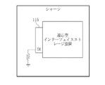
図1を参照すると、幾つかの実施形態で、適応型インターフェイスストレージ装置(adaptive interface storage device)は、後端ストレージインターフェイスコネクター105、適応可能(adaptable)回路110、前端ストレージインターフェイスコネクター115、及び、前端ストレージインターフェイスコネクター115と適応可能回路110との間に連結された前端マルチプレクサー120、を含む。このような構成要素は、後端ストレージインターフェイスコネクター105を通じて固定インターフェイスストレージ装置107(例えば、NVMe(nonvolatile memory express)、SSD(Solid State Drive)等)に連結されるアダプターモジュールとして動作し、ホストシャーシに1つ以上のストレージインターフェイスをサポートするストレージディバイスとして動作する。前端マルチプレクサーは、一般的に、信号を複数の利用可能である経路の中で1つにルーティングするための任意の適切な回路であるルーティング又はスイッチング回路の例示である。2つ以上の経路が利用可能である場合、PCIe(Peripheral Component Interconnect express)スイッチのようなルーティング構成要素が使用される。一例として、ルーティングは、単なる2つの構成要素の間に存在し得る。
Referring to FIG. 1, in some embodiments, an adaptive interface storage device includes a rear end
幾つかの実施形態で、適応型インターフェイスストレージ装置は(i)3.5インチハードドライブフォームファクタ(又は“LFF(Large From Factor)”標準、又は(ii)2.5インチハードドライブフォームファクタ(又はSFF(Small Form Dactor))、又は(iii)例えば、FH-FLカードアウトライン(Full-Height、Full Length card outline)のような標準PCIeカードフォームファクタ、又はFH-HLアウトライン(Full-Height、Half Length outline)に従っている。 In some embodiments, the adaptive interface storage device is (i) a 3.5 inch hard drive form factor (or "LFF (Large From Factor)" standard), or (ii) a 2.5 inch hard drive form factor (or SFF (Small Form Dactor), or (iii) standard PCIe card form factors, such as FH-FL card outline (Full-Height, Full Length card outline), or FH-HL outline (Full-Height, Half Length). outline).
本明細書で使用される、“ストレージインターフェイス”は、(i)ストレージ装置(例えば、ハードドライブ又はSSDのような永久ストレージ装置)、及び、(ii)ストレージ装置に連結されるマザーボード又はプロセッサのようなホストとの間のインターフェイスである。幾つかの実施形態で、ホストは、電力及び機械的なサポート(マウンティング及び冷却)を提供し、ストレージ装置に連結され、他のホスト(例えば、サーバー)とストレージ装置との間の連結を提供するシャーシである。これと関連して、永久ストレージ装置とホストとの間のストレージインターフェイスで、ホストは、ストレージ装置に対する“ホスト側ストレージインターフェイス”、例えば、ホスト側NVMeストレージインターフェイスを提供し(例えば、ホストは命令(例えば、読出し又は書込み命令)をNVMeインターフェイスを通じてストレージ装置に伝送し)、ストレージ装置は、“装置側ストレージ装置インターフェイス”、例えば装置側NVMeストレージ装置インターフェイスをホストに提供する。他の例示として、ストレージインターフェイスは“NVMeoF(NVMe over Fabrics)”である。 As used herein, a "storage interface" includes (i) a storage device (e.g., a permanent storage device such as a hard drive or SSD) and (ii) a device such as a motherboard or processor that is coupled to the storage device. It is the interface between the host In some embodiments, hosts provide power and mechanical support (mounting and cooling), are coupled to storage devices, and provide connectivity between other hosts (e.g., servers) and storage devices. Chassis. Relatedly, in the storage interface between the persistent storage device and the host, the host provides a "host-side storage interface" to the storage device, e.g. , read or write command) to the storage device through the NVMe interface), and the storage device provides a “device-side storage device interface”, eg, a device-side NVMe storage device interface, to the host. As another example, the storage interface is "NVMeoF (NVMe over Fabrics)".
適応可能回路110は、FPGA(Field Programmable Gate Array)のようなプログラマブル(programmable)論理回路である。図1の実施形態は、適応可能回路110と前端ストレージインターフェイスコネクター115との間の1つ以上の連結(“イーサーネット連結”と称される)125を形成する1つ以上のコンダクターのセットをさらに含むことができ、適応可能回路110は、動作の幾つかのモード(又は“状態”)で、1つ以上のイーサーネットインターフェイス(例えば、図示されたように2つのイーサーネットインターフェイス)をイーサーネット連結125で提供するように構成される。前端ストレージインターフェイスコネクター115はU.2コネクターであり、U.2コネクターのSASポート0及びSASポート1ピンは、イーサーネット連結のために使用されることができる。
図1の適応型インターフェイスストレージ装置は、2つの状態、第1状態及び第2状態で動作するように構成される;第1状態において、適応型インターフェイスストレージ装置は、前端ストレージインターフェイスコネクターで第1ストレージプロトコル(例えば、“NVMe”)に従って装置側ストレージインターフェイスを提供するように構成され、第2状態において、適応型インターフェイスストレージ装置は、前端ストレージインターフェイスコネクター115で第2ストレージプロトコル(例えば、“NVMe over Fabrics”)に従って装置側ストレージインターフェイスを提供するように構成されている。 The adaptive interface storage device of Figure 1 is configured to operate in two states, a first state and a second state; configured to provide a device-side storage interface according to a protocol (eg, "NVMe"), and in a second state, the adaptive interface storage device provides a second storage protocol (eg, "NVMe over Fabrics ”) to provide a device-side storage interface.
前端マルチプレクサー120は、2つの異なる装置側ストレージインターフェイスをサポートするために、第1状態及び第2状態で異なるように構成される。前端マルチプレクサー120は、図1に示されるように、第1マルチプレクサーチャンネル121と第2マルチプレクサーチャンネル122とを含む。第1マルチプレクサーチャンネル121及び第2マルチプレクサーチャンネル122の各々は、以下でさらに詳細に論議されるように制御される。幾つかの実施形態で、前端マルチプレクサー120、例えばクワッド1:2-2:1マルチプレクサーは、“Texas Instruments”から購入可能なモデル“SN65LVCP114”集積回路のような信号コンディショニングを含む線形リドライバー(redriver)で具現される。
The front-
本明細書で使用されるように、マルチプレクサーは、1つの共通ポート、2つ以上の選択可能(selectable)ポート、及び選択入力を有する装置である。動作の時、選択入力で受信された選択信号に応じて、マルチプレクサーは、共通ポートと選択可能ポートとの中で1つのポート(“選択されたポート”と称される)を連結する(即ち、それらの間で内部接続を作る)。各ポートは、1つのレーン幅又は様々なレーンの幅である。ポートの全てのレーンは、入力レーン又は出力レーンであり、ポートは、入力レーン及び出力レーンの組み合わせを含む。(出力レーンを有しない)共通入力ポート及び複数の選択可能出力レーンを含むマルチプレクサーは、デマルチプレクサー(de-multiplexer)と称されることもある。様々なレーン幅を有する共通ポートを有するマルチプレクサーは(“マルチプレクサーチャンネル”と称される)、複数のマルチプレクサーと同等であり、各マルチプレクサーチャンネルはさらに少ないレーンを有し(これによってマルチプレクサーチャンネルの総レーン数がマルチプレクサーのレーン数と同一である)、共有された選択入力連結を有する(即ち、各々が同一な選択信号ソースに連結された選択入力を有する)。幾つかの実施形態で、複数のマルチプレクサーチャンネルが、単一集積回路(“Texas Instruments”から購入可能なモデル“SN65LVCP114”集積回路など)に含まれてよい。このような集積回路は、例として4つの独立なチャンネル(各々が1つのレーン幅)を含み、各々が別の独立な選択入力を有するので、集積回路は、4つの選択入力を有する。 As used herein, a multiplexer is a device that has one common port, two or more selectable ports, and a select input. In operation, the multiplexer links one port (referred to as the "selected port") among the common port and the selectable port in response to the select signal received at the select input. , making an internal connection between them). Each port is one lane wide or various lanes wide. All lanes of a port are input lanes or output lanes, and a port includes a combination of input and output lanes. A multiplexer that includes a common input port (with no output lanes) and multiple selectable output lanes is sometimes referred to as a de-multiplexer. A multiplexer that has a common port with varying lane widths (referred to as a "multiplexer channel") is equivalent to multiple multiplexers, with each multiplexer channel having even fewer lanes (thereby multiplexing (the total number of lanes in the channel is the same as the number of lanes in the multiplexer), and have shared select input connections (ie, each has a select input connected to the same select signal source). In some embodiments, multiple multiplexer channels may be included in a single integrated circuit (such as the model "SN65LVCP114" integrated circuit available from "Texas Instruments"). Such an integrated circuit illustratively includes four independent channels (each one lane wide) each having another independent select input, so the integrated circuit has four select inputs.
このように、“Texas Instruments”で購入することができるモデル“SN65LVCP114”のような信号コンディショニングを有する線形リドライバーであるクワッド1:2-2:1マルチプレクサーが採用される場合には、単一マルチプレクサー(例えば、前端マルチプレクサー120)、又は2つのマルチプレクサーチャンネル(第1マルチプレクサーチャンネル121及び第2マルチプレクサーチャンネル122)、又は8個のマルチプレクサーチャンネルとして称され、各々は、1つのレーン幅を有する(共に4つの入力レーン及び4つの出力レーン提供する)。
Thus, if a quad 1:2-2:1 multiplexer that is a linear redriver with signal conditioning such as model SN65LVCP114 available from Texas Instruments is employed, a single Referred to as a multiplexer (e.g., front-end multiplexer 120), or two multiplexer channels (
適応可能回路110は、以下で、さらに具体的に説明されるように、前端ストレージインターフェイスコネクター115で、装置側ストレージインターフェイス又は制御プレーンインターフェイスの具現の一部を形成する、第1PCIeエンドポイント141及び第2PCIeエンドポイント142を含む。後端ストレージインターフェイスコネクター105で、後端ストレージインターフェイスコネクター105と連結される固定インターフェイスストレージ装置107にホスト側ストレージインターフェイスを具現するための1つ以上のPCIeルートポート(又は、ルートコンプレックス)150も含む。
The
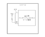
図2Aを参照すると、幾つかの実施形態では、適応型インターフェイスストレージ装置が第1状態で動作する時、第1マルチプレクサーチャンネルの第1選択可能ポートが選択され、第2マルチプレクサーチャンネルの第1選択可能ポートが選択される。図2Aでは、異なる環境(例えば、適応型インターフェイスストレージ装置が第2状態で動作する時)でこれらの連結を生成するコンダクターが存在するにも拘らず、このような構成は、容易な理解のために、第1マルチプレクサーチャンネルの第2選択可能ポート及び第2マルチプレクサーチャンネルの第2選択可能ポートで終わるラインを図面から省略することによって図示されている。第2PCIeエンドポイント142は、((以下でさらに具体的に説明されるように)適応可能回路110のプログラミングの結果として)存在しないか、或いは(選択されない第2マルチプレクサーチャンネルの第2選択可能であるポートの結果として)存在するが、使用されないことがある。同様に、適応可能インターフェイスストレージ装置が(適応可能回路110のプログラミングの結果として)第1状態で動作する時、イーサーネット連結125は、動作可能である;容易な理解のために、イーサーネット連結によって採用されるコンダクターが(例えば、適応型インターフェイスストレージ装置が第2状態で動作する時)存在するにも拘らず、イーサーネット連結125を示す(例えば、図1で)ラインを図2Aから省略することによって図示されている。
Referring to FIG. 2A, in some embodiments, when the adaptive interface storage device operates in the first state, the first selectable port of the first multiplexer channel is selected and the first selectable port of the second multiplexer channel is selected. A selectable port is selected. Although in FIG. 2A there are conductors creating these connections in different environments (eg, when the adaptive interface storage device operates in the second state), such a configuration is for ease of understanding. , by omitting from the drawing the lines ending in the second selectable port of the first multiplexer channel and the second selectable port of the second multiplexer channel. The
第1状態において、前端ストレージインターフェイスコネクター115に存在する装置側ストレージインターフェイスは、NVMeである。適応型インターフェイスストレージ装置は、ホスト(例えば、以下でさらに具体的に説明されるように、適応型インターフェイスストレージ装置を収容するシャーシに連結されたホスト)からNVMe命令を受信し、その命令は、前端マルチプレクサー120、適応可能回路110、及び後端ストレージインターフェイスコネクター105を通じて、固定インターフェイスストレージ装置107に伝送される。固定インターフェイスストレージ装置107は、各命令を処理し、適応型インターフェイスストレージ装置が、適応可能回路110、前端マルチプレクサー120、及び前端ストレージインターフェイスコネクター115を通じて、ホストに伝達する命令応答を、受信された各命令に応答して伝送する。適応可能インターフェイスストレージ装置は、1x4NVMe装置側ストレージインターフェイスをホストに提供する。第1PCIeエンドポイント141は、1x4PCIeエンドポイントである;1x4NVMe装置側ストレージインターフェイスの4つのレーンの中で2つ(例えば、第1番目の2つのレーン、レーン“0”及び“1”)は、第1マルチプレクサーチャンネル121を通じて第1PCIeエンドポイント141に連結され、4つのレーンの中で他の2つ(例えば、第3及び第4レーン、レーン“2”及び“3”)は、第2マルチプレクサーチャンネル122を通じて第1PCIeエンドポイント141と連結されている。
In the first state, the device-side storage interface present at the front-end
図2Bを参照すると、幾つかの実施形態で、適応型インターフェイスストレージ装置は、第2状態で動作する時、第1マルチプレクサーチャンネルの第1選択可能ポートが選択され、第2マルチプレクサーチャンネルの第2選択可能ポートが選択される。図2Bで、(例えば、適応型インターフェイスストレージ装置が第1状態で動作する時)他の環境でこのような連結を生成するコンダクターが存在するにも拘らず、容易な理解のために、この構成は、第1マルチプレクサーチャンネルの第2選択可能ポート及び第2マルチプレクサーチャンネルの第1選択可能ポートで終わるラインを図面から省略することによって図示されている。 Referring to FIG. 2B, in some embodiments, when the adaptive interface storage device operates in the second state, the first selectable port of the first multiplexer channel is selected and the first selectable port of the second multiplexer channel is selected. 2 selectable ports are selected. In FIG. 2B, for ease of understanding, this configuration is shown even though there are conductors that create such connections in other environments (eg, when the adaptive interface storage device operates in the first state). is illustrated by omitting from the drawing the lines ending in the second selectable port of the first multiplexer channel and the first selectable port of the second multiplexer channel.
第2状態において、前端ストレージインターフェイスコネクター115で提供された装置側ストレージインターフェイスは、1つ以上のイーサーネット連結125上の“NVMe over Fabrics”である。適応型インターフェイスストレージ装置は、イーサーネット連結125を通じて“NVMe over Fabrics”命令を受信し、その命令は、適応可能回路110及び後端ストレージインターフェイスコネクター105を通じて、固定インターフェイスストレージ装置107に伝達される。適応可能回路110は、前端ストレージインターフェイスコネクター115で採用される“NVMe over Fabrics”ストレージプロトコルと後端ストレージインターフェイスコネクター105で採用されるNVMeストレージプロトコルとの間の変換のためのイーサーネット-NVMeブリッジ210を含む。
In the second state, the device-side storage interface provided at front-end
適応型インターフェイスストレージ装置が第1状態で動作する時のように、適応型インターフェイスストレージ装置が第2状態で動作する時、固定インターフェイスストレージ装置107は、ストレージ装置107が受信した各命令を処理して、各々の受信された命令に対して後端ストレージインターフェイスコネクター105を通じて適応型インターフェイスストレージ装置が適応可能回路110及び前端ストレージインターフェイスコネクター115を通じて戻して伝送する命令応答を伝送する。適応型インターフェイスストレージ装置は、“NVMe over Fabrics”装置側ストレージインターフェイスをホストに提供する。
When the adaptive interface storage device operates in the second state, such as when the adaptive interface storage device operates in the first state, the fixed
適応型インターフェイスストレージ装置が第2状態で動作する時、第1PCIeエンドポイント141は、1x4PCIeエンドポイントであり、第2PCIeエンドポイント142も1x4PCIeエンドポイントである;第1PCIeエンドポイント141及び第2PCIeエンドポイント142が、共に第1前端ストレージインターフェイスコネクター115で第1マルチプレクサーチャンネル121及び第2マルチプレクサーチャンネル122を通じて制御プレーン動作のための2x2PCIeリンクを提供する。このような制御プレーン動作は、例として、固定インターフェイスストレージ装置107の消去コードをアップデートするか、或いは適応型インターフェイスストレージ装置でファームウェアをアップグレードすることを含む。
When the adaptive interface storage device operates in the second state, the
図2A及び図2Bから分かるように、第1マルチプレクサーチャンネル121の状態は、適応型インターフェイスストレージ装置の第1状態及び適応型インターフェイスストレージ装置の第2状態で同一である(そして、第1マルチプレクサーチャンネル121の第2選択可能ポートは“連結されない”、即ち、他のどの構成要素とも連結されない)。第2マルチプレクサーチャンネル122を通じて連結されたPCIeレーンに遅延等化(delay equalization)を提供するためのシステムに含まれる。適応型インターフェイスストレージ装置が第1状態で動作する時及び適応型ストレージ装置が第2状態で動作する時、全ての適応型インターフェイスストレージ装置は、ホスト側“1x4NVMe”ストレージインターフェイスを固定インターフェイスストレージ装置107に提供し、以後、装置側“1x4NVMe”ストレージインターフェイスを適応型インターフェイスストレージ装置に提供する。
As can be seen from FIGS. 2A and 2B, the state of the
図3A及び図3Bを参照すると、幾つかの実施形態で、以上言及されたように、適応型インターフェイスストレージ装置が、シャーシに設置されている。適応型インターフェイスストレージ装置は、第1状態及び第2状態の間で選択するための信号を受信するピン(例えば、前端ストレージインターフェイスコネクター115がU.2コネクターである場合、U.2コネクターの”E6”ピン)を有する。シャーシは、第1状態で動作する適応型インターフェイスストレージ装置に信号するための接地電圧(図3Aのように)、又は第2状態で動作する適応型インターフェイスストレージ装置に信号するための“Vdd”(図3Bのように)にピンを連結する配線(wiring)を有する。以下でさらに具体的に説明されるように、適応型インターフェイスストレージ装置の回路は、適応型インターフェイスストレージ装置が信号(例えば、“E6”ピンで受信された信号)により、前端マルチプレクサー120をセッティングすることによって、及び適応可能回路110をプログラミングすることによって識別された状態で動作するように惹起する。
Referring to Figures 3A and 3B, in some embodiments, adaptive interface storage devices, as mentioned above, are installed in a chassis. The adaptive interface storage device has a pin that receives a signal to select between the first state and the second state (e.g., "E6" on the U.2 connector if the front end
図4を参照すると、幾つかの実施形態で、(適応可能回路110の構成ポート(例えば、適応可能回路110のSPI(Serial Peripheral Interface)構成ポート)を通じて)開始される時、適応可能回路110によってロードされたビットファイルは、適応型インターフェイスストレージ装置が動作中である時の状態に基づいて選択される。例として、適応型インターフェイスストレージ装置が第1状態において動作する時、ビットファイルマルチプレクサー410は適応可能回路110の構成ポートを第1状態で動作するための適応可能回路110を構成するためのビットファイルを格納する第1メモリ421(例えば、SPIフラッシュメモリ)と連結させ、第2状態において、ビットファイルマルチプレクサー410は、適応可能回路110の構成ポートを第2状態で動作するための適応可能回路110を構成するためのビットファイルを格納する第2メモリ422(例えば、SPIフラッシュメモリ)と連結させる。これによって、メモリ421は、第1状態のためのビットファイルのみを格納し、メモリ422は第2状態のためのビットファイルのみを格納することができる。第1メモリ421及び第2メモリ422の各々のビットファイルの1つは、PCIe部分を含み、PCIe部分は、適応可能回路110に読み出し、先ず具現され、PCIeエンドポイント141と142、及びルートポイント150が、PCIeリンクトレーニングに正確な時間に参与するように構成されるように引き起こす。適応可能回路110の残りは、PCIeリンクトレーニングが発生する間又はPCIeリンクトレーニングが成功的に完了された後、もしくは、PCIeトレーニングの間及びPCIeトレーニングの後で、全てに構成される。(前端マルチプレクサー120によって生成される連結を適応可能回路110にプログラミングする代わりに)外部ハードウェア前端マルチプレクサー120を使用することは、適応可能回路110を構成することがPCIeリンクのトレーニングのためのPCIe標準によって割り当てられた時間より長い時間を消耗する場合に発生し得る問題を回避することができる。
Referring to FIG. 4, in some embodiments, when initiated (through a configuration port of adaptable circuit 110 (e.g., a serial peripheral interface (SPI) configuration port of adaptable circuit 110),
たとえ、ここでは、“第1”、“第2”、“第3”等の用語が、多様な要素、成分、領域、層、及び/又はセクションを説明するために使用されていても、このような要素、成分、領域、層、及び/又はセクションは、このような用語によって限定されないことが理解されるべきである。このような用語は、他の要素、成分、領域、層、又はセクションから1つの要素、構成、領域、層又はセクションを区別するために使用される。従って、後述する第1構成要素、成分、領域、層、又はセクションは、本発明の思想及び範囲を逸脱することなく、第2構成要素、成分、領域、層、又はセクションを指称することができる。 Even though the terms "first," "second," "third," etc. are used herein to describe various elements, components, regions, layers, and/or sections, this It should be understood that such elements, components, regions, layers and/or sections are not limited by such terms. Such terms are used to distinguish one element, composition, region, layer or section from another element, component, region, layer or section. Thus, reference to a first component, component, region, layer or section discussed below could refer to a second component, component, region, layer or section without departing from the spirit and scope of the present invention. .
1つの要素又は図面で図示された他の構成要素又は特徴との特徴的な関係を説明することを容易にするために“下の”、“下”、“低い”、“特定部分の下”、“上に”、“上部”と同一の、空間的であり、相対的な用語が、ここにおいて使用され得る。空間的であり、相対的な用語は、図面で示された方向に加えて、使用又は動作で装置の他の方向を含むように意図されることが理解されるべきである。例えば、仮に、図面の装置を裏返したら、他の構成要素又は特徴の“下”又は“下の”又は“特定部分の下”として説明された構成要素は、他の構成要素又は特徴の“上に”合わせられるようになる。従って、“下の”又は“特定部分の下”の例示的な用語は、上又は下方向の全てを含むことができる。装置は、異なって合わせられ(例えば、90°又は他の方向に回転されること)、そして、空間的であり相対的な技術語は、それに従って解釈されなければならない。また、2層の“間に”と指称される時、2層の間に1つの層のみがあるか、又は、1つ以上の間の層が存在することも、また理解されるべきである。 "Below", "below", "lower", "below a particular portion" to facilitate describing the characteristic relationships of one element or other components or features illustrated in the drawings. , "above", "upper", and the same spatial and relative terms may be used herein. It should be understood that spatial and relative terms are intended to include other orientations of the device in use or operation in addition to the orientation shown in the drawings. For example, if the device in the drawings were turned over, a component described as "below" or "beneath" other components or features or "below certain portions" would be "above" other components or features. It will be able to be adjusted to Thus, the exemplary terms "below" or "below a particular portion" can include all directions above or below. Devices may be aligned differently (eg, rotated 90° or in other directions), and spatial and relative terms should be interpreted accordingly. Also, when referring to "between" two layers, it should also be understood that there may be only one layer between the two layers or there may be more than one layer between them. .
本明細書で使用された用語は、単に特定の実施形態を説明するためのものであり、本発明を限定しようとすることを意図するものではない。本明細書で使用されるように、“大体”、“約”の用語、及びこれらと同様な用語は、近似する用語として使用され、程度の用語としては、使用されなく、本発明の当業者によって識別される測定され又は計算された値の固有な変動を考慮するように意図されている。 The terminology used herein is for the purpose of describing particular embodiments only and is not intended to be limiting of the invention. As used herein, the terms "approximately," "about," and like terms are used as terms of approximation and not as terms of degree, and are intended to is intended to account for inherent variations in the measured or calculated values identified by
本明細書で使用されるように、文脈上で明確に異なるように指示されない限り、単数形態は、本発明の概念の説明及び付加された請求項に使用される時、複数の形態を含むものと意図されている。そして、“含む”又は“含み、限定されない”の用語が本明細書に使用される場合は、記述された特徴、領域、数字、段階、動作、構成、及び/又は部品の存在を明記することであり、これらの1つ又はそれ以上の他の特徴、数字、段階、動作、構成、部品、及び/又は、グループの存在又は付加を排除しないものと、さらに理解されなければならない。本明細書で使用されるように、“及び/又は”の用語は、1つ以上の関連した羅列されたアイテムの任意の、及び、全ての組み合わせを含む。“少なくとも1つ”のような表現は、要素の全体リーストを修正し、そしてリーストの個別要素を修正しない。また、“することができる”の使用は、本発明の実施形態を説明する時、“本発明の1つ以上の実施形態”を称する。また、“例示的な”の用語は、例示又は実施形態を指称するように意図されている。本明細書で使用されたように、“使用する”、“使う”、及び“使用された“の用語は、“利用する”、“利用している”、そして“利用された”の用語の同意語であると各々看做され得る。 As used herein, the singular forms include the plural forms when used in describing the inventive concept and in the appended claims, unless the context clearly dictates otherwise. is intended. and when the terms "including" or "including but not limited to" are used herein, specify the presence of the described features, regions, numbers, steps, acts, configurations, and/or parts. and does not exclude the presence or addition of one or more of these other features, figures, steps, acts, configurations, parts and/or groups. As used herein, the term "and/or" includes any and all combinations of one or more of the associated listed items. Expressions such as "at least one" modify the entire list of elements and not individual elements of the list. Also, the use of "can" refers to "one or more embodiments of the invention" when describing embodiments of the invention. Also, the word "exemplary" is intended to refer to an illustration or embodiment. As used herein, the terms "use," "use," and "used" are synonymous with the terms "utilize," "utilize," and "utilized." Each can be considered synonymous.
構成要素又はレイヤーが他の構成要素又はレイヤーと“上にある”、”連結される”、“結合される”、又は“隣接する”と言及される時は、他の構成要素又はレイヤー上に直接的にあるか、連結させるか、或いは結合されるか、或いは隣接することができ、もしくは、1つ以上の間に位置する構成要素又はレイヤーが存在することができる。反面、構成要素が他の構成要素又はレイヤーに“直接的に上にある”、“直接的に連結される”、“直接的に結合される”、又は“直ぐ隣接する”と言及される時は、間に位置する構成要素又はレイヤーが存在しない。 When a component or layer is referred to as being “over,” “coupled with,” “coupled with,” or “adjacent to” another component or layer, They may be direct, connected, joined, or adjacent, or there may be one or more intervening components or layers. Conversely, when a component is referred to as being "directly overlying," "directly coupled," "directly coupled to," or "immediately adjacent to" another component or layer. has no intervening components or layers.
本明細書で羅列された任意の数の範囲は、羅列された範囲内に含まれる同一な数の正確性の全ての下位範囲を含むように意図されている。例として、“1.0で10.0”の範囲は羅列された最小値1.0と羅列された最大値10.0との間の(そして含まれた)全ての下位範囲を含むするように、即ち、例として、2.4で7.6のように、1.0と同一であるか、又は、大きい最小値及び10.0と同一であるか、もしくは、小さい最小値を有する下位グループを含むように意図されている。本明細書で羅列された任意の最大数の制限は、ここに含まれる全てのさらに低い数の制限を含むように意図され、本明細書で羅列された任意の最小数の制限は、ここに含まれた全てのさらに高い数の制限を含むするように意図される。 Any numerical range recited herein is intended to include all subranges of the same numerical precision subsumed within the recited range. As an example, a range of "1.0 to 10.0" would include all subranges between (and inclusive) the listed minimum value of 1.0 and the listed maximum value of 10.0. i.e., sub Intended to contain groups. Any maximum numerical limitation recited herein is intended to include all lower numerical limitations contained herein, and any minimum numerical limitation recited herein is intended to include all lower numerical limitations contained herein. It is intended to include all higher numerical limitations included.
本明細書では、適応型インターフェイスストレージ装置の例示的な実施形態が具体的に説明され図示されたが、多くの修正と変形が当業者にとっては明確である。従って、本開示の原理に従って説明される適応型インターフェイスストレージ装置について、本明細書で具体的に説明されること以外の実施形態が具現できることが理解されるべきである。 Although exemplary embodiments of adaptive interface storage devices have been specifically described and illustrated herein, many modifications and variations will be apparent to those skilled in the art. Thus, it should be understood that embodiments of adaptive interface storage devices described in accordance with the principles of the present disclosure may be implemented other than those specifically described herein.
105 後端ストレージインターフェイスコネクター
107 固定インターフェイスストレージ装置
110 適応可能回路
115 前端ストレージインターフェイスコネクター
120 前端マルチプレクサー
121 第1マルチプレクサーチャンネル
122 第2マルチプレクサーチャンネル
125 イーサーネット連結
141 第1PCIeエンドポイント
142 第2PCIeエンドポイント
150 PCleルートポイント
210 イーサーネットNVMeブリッジ
105 rear end
Claims (14)
前記第1コネクターに接続された第1回路と、
前記第1回路に接続された第2回路と、
前記第2回路に接続された第2コネクターと、
を含み、
前記第1回路は、第1エンドポイントおよび第2エンドポイントを含み、
前記第2回路は、第1マルチプレクサーであって、
第1マルチプレクサーチャンネルであり、
前記第2コネクターに接続された、第1マルチプレクサーチャンネル共通ポートと、
前記第1エンドポイントに接続された、第1マルチプレクサーチャンネル第1選択可能ポートと、
接続されていない、第1マルチプレクサーチャンネル第2選択可能ポートと、
を有する、第1マルチプレクサーチャンネルと、
第2マルチプレクサーチャンネルであり、
前記第2コネクターに接続された、第2マルチプレクサーチャンネル共通ポートと、
前記第1エンドポイントに接続された、第2マルチプレクサーチャンネル第1選択可能ポートと、
前記第2エンドポイントに接続された第2マルチプレクサーチャンネル第2選択可能ポートと、
を有する、第2マルチプレクサーチャンネルと、
を含む、装置であって、
前記装置は、第1状態または第2状態で動作するように構成されており、
前記第1状態では、前記第1マルチプレクサーチャンネル第1選択可能ポートが選択され、かつ、前記第2マルチプレクサーチャンネル第1選択可能ポートが選択されており、
前記第2状態では、前記第1マルチプレクサーチャンネル第1選択可能ポートが選択され、かつ、前記第2マルチプレクサーチャンネル第2選択可能ポートが選択されており、
前記装置は、
前記第1状態において、前記第2コネクターで、第1プロトコルに従って第1インターフェイスを提供し、かつ、
前記第2状態において、前記第2コネクターで、前記第1プロトコルとは異なる第2プロトコルに従って、第2インターフェイスを提供する、
ように構成されている、
装置。 a first connector;
a first circuit connected to the first connector;
a second circuit connected to the first circuit;
a second connector connected to the second circuit;
including
the first circuit includes a first endpoint and a second endpoint;
The second circuit is a first multiplexer,
a first multiplexer channel,
a first multiplexer channel common port connected to the second connector;
a first multiplexer channel first selectable port connected to the first endpoint;
a first multiplexer channel second selectable port that is not connected;
a first multiplexer channel having
a second multiplexer channel,
a second multiplexer channel common port connected to the second connector;
a second multiplexer channel first selectable port connected to the first endpoint;
a second multiplexer channel second selectable port connected to the second endpoint;
a second multiplexer channel having
An apparatus comprising
the device is configured to operate in a first state or a second state;
in the first state, the first multiplexer channel first selectable port is selected and the second multiplexer channel first selectable port is selected;
in the second state, the first multiplexer channel first selectable port is selected and the second multiplexer channel second selectable port is selected;
The device comprises:
providing a first interface according to a first protocol at the second connector in the first state; and
providing a second interface at the second connector in the second state according to a second protocol different from the first protocol;
configured as
Device.
請求項1に記載の装置。 wherein the first protocol is NVMe;
A device according to claim 1 .
請求項2に記載の装置。 wherein the second protocol is NVMeoF (NVMe over Fabrics);
3. Apparatus according to claim 2 .
請求項1に記載の装置。 The device is further configured to provide a first control plane interface at the second connector in the second state.
A device according to claim 1 .
前記第2エンドポイントは、4レーンエンドポイントであり、かつ、
前記第1マルチプレクサーチャンネル共通ポートおよび前記第2マルチプレクサーチャンネル共通ポートは、合わせて、2つの入力レーンおよび2つの出力レーンを有する、
請求項1に記載の装置。 the first endpoint is a 4-lane endpoint;
the second endpoint is a 4-lane endpoint, and
the first multiplexer channel common port and the second multiplexer channel common port collectively have two input lanes and two output lanes;
A device according to claim 1 .
請求項1に記載の装置。 said first circuit being a programmable adaptable circuit having a configuration port and configured to load a bitfile through said configuration port at system startup;
A device according to claim 1 .
第1ビットファイルメモリと、
第2ビットファイルメモリと、
第2マルチプレクサーと、
を含み、
前記第2マルチプレクサーは、
前記構成ポートに接続された第2マルチプレクサー共通ポートと、
前記第1ビットファイルメモリに接続された第2マルチプレクサーの第1選択可能ポートと、
前記第2ビットファイルメモリに接続された第2マルチプレクサーの第2選択可能ポートと、
を有する、
請求項6に記載の装置。 The device further comprises:
a first bit file memory;
a second bit file memory;
a second multiplexer;
including
The second multiplexer is
a second multiplexer common port connected to the configuration port;
a first selectable port of a second multiplexer connected to the first bitfile memory;
a second selectable port of a second multiplexer connected to the second bitfile memory;
having
7. Apparatus according to claim 6 .
前記第2状態では、前記第2マルチプレクサーの第2選択可能ポートが選択される、
請求項7に記載の装置。 in the first state a first selectable port of the second multiplexer is selected; and
in the second state a second selectable port of the second multiplexer is selected;
8. Apparatus according to claim 7 .
請求項1に記載の装置。 The second connector is a U.S.C. 2 connectors,
A device according to claim 1 .
前記第1状態と前記第2状態との間を選択するための信号を受信するように構成されている状態制御入力、
を含む、請求項1に記載の装置。 The device further comprises:
a state control input configured to receive a signal to select between the first state and the second state;
2. The device of claim 1, comprising:
前記状態制御入力は、前記E6ピンである、
請求項10に記載の装置。 The second connector is a U.S.C. 2 connectors, and
the state control input is the E6 pin;
11. Apparatus according to claim 10 .
前記第1状態では、前記第2コネクターで、装置側NVMeストレージインターフェイスを提供し、かつ、
前記第2状態では、前記第2コネクターで、装置側NVMeoFストレージインターフェイスを提供する、
ように構成されている、
請求項1に記載の装置。 The device comprises:
in the first state, the second connector provides a device-side NVMe storage interface; and
in the second state, providing a device-side NVMeoF storage interface at the second connector;
configured as
A device according to claim 1 .
請求項1乃至12いずれか一項に記載の装置と、
を含む、システム。 a chassis;
a device according to any one of claims 1 to 12 ;
system , including
前記シャーシは、前記第1状態を選択する信号を前記状態制御入力へ供給するようにハードワイヤ処理されている、
請求項13に記載のシステム。 the device further includes a state control input configured to receive a signal for selecting between the first state and the second state; and
the chassis is hardwired to provide a signal to the state control input that selects the first state;
14. The system of claim 13 .
Applications Claiming Priority (4)
| Application Number | Priority Date | Filing Date | Title |
|---|---|---|---|
| US201862641246P | 2018-03-09 | 2018-03-09 | |
| US62/641,246 | 2018-03-09 | ||
| US16/020,923 | 2018-06-27 | ||
| US16/020,923 US10521378B2 (en) | 2018-03-09 | 2018-06-27 | Adaptive interface storage device with multiple storage protocols including NVME and NVME over fabrics storage devices |
Publications (3)
| Publication Number | Publication Date |
|---|---|
| JP2019160307A JP2019160307A (en) | 2019-09-19 |
| JP2019160307A5 JP2019160307A5 (en) | 2022-02-07 |
| JP7206130B2 true JP7206130B2 (en) | 2023-01-17 |
Family
ID=67842668
Family Applications (1)
| Application Number | Title | Priority Date | Filing Date |
|---|---|---|---|
| JP2019034566A Active JP7206130B2 (en) | 2018-03-09 | 2019-02-27 | adaptive interface storage device |
Country Status (5)
| Country | Link |
|---|---|
| US (4) | US10521378B2 (en) |
| JP (1) | JP7206130B2 (en) |
| KR (1) | KR102457658B1 (en) |
| CN (2) | CN110245104B (en) |
| TW (1) | TWI796398B (en) |
Families Citing this family (10)
| Publication number | Priority date | Publication date | Assignee | Title |
|---|---|---|---|---|
| US11461258B2 (en) | 2016-09-14 | 2022-10-04 | Samsung Electronics Co., Ltd. | Self-configuring baseboard management controller (BMC) |
| US10372659B2 (en) | 2016-07-26 | 2019-08-06 | Samsung Electronics Co., Ltd. | Multi-mode NMVE over fabrics devices |
| US10210123B2 (en) | 2016-07-26 | 2019-02-19 | Samsung Electronics Co., Ltd. | System and method for supporting multi-path and/or multi-mode NMVe over fabrics devices |
| US11144496B2 (en) | 2016-07-26 | 2021-10-12 | Samsung Electronics Co., Ltd. | Self-configuring SSD multi-protocol support in host-less environment |
| US20190109720A1 (en) | 2016-07-26 | 2019-04-11 | Samsung Electronics Co., Ltd. | Modular system (switch boards and mid-plane) for supporting 50g or 100g ethernet speeds of fpga+ssd |
| US10346041B2 (en) | 2016-09-14 | 2019-07-09 | Samsung Electronics Co., Ltd. | Method for using BMC as proxy NVMeoF discovery controller to provide NVM subsystems to host |
| US10521378B2 (en) | 2018-03-09 | 2019-12-31 | Samsung Electronics Co., Ltd. | Adaptive interface storage device with multiple storage protocols including NVME and NVME over fabrics storage devices |
| CN111383154A (en) * | 2020-04-02 | 2020-07-07 | 广东金宇恒软件科技有限公司 | Data interface and public financial budget management integrated platform system convenient to manage |
| TWI759772B (en) * | 2020-06-19 | 2022-04-01 | 英業達股份有限公司 | Pcie data transmission control system |
| US11770271B2 (en) | 2020-08-21 | 2023-09-26 | Samsung Electronics Co., Ltd. | Data center |
Citations (3)
| Publication number | Priority date | Publication date | Assignee | Title |
|---|---|---|---|---|
| JP2015528608A (en) | 2012-09-19 | 2015-09-28 | コンバーサント・インテレクチュアル・プロパティ・マネジメント・インコーポレイテッドConversant Intellectual Property Management Inc. | Flash memory controller with dual mode pinout |
| US20170185554A1 (en) | 2015-12-28 | 2017-06-29 | Emc Corporation | Fabric for modular solid-state storage systems |
| JP2018018514A (en) | 2016-07-26 | 2018-02-01 | 三星電子株式会社Samsung Electronics Co.,Ltd. | Storage device operative in multiple modes, and system including the same |
Family Cites Families (26)
| Publication number | Priority date | Publication date | Assignee | Title |
|---|---|---|---|---|
| US20050251609A1 (en) * | 2004-05-04 | 2005-11-10 | Horng-Yee Chou | Removable peripheral device |
| CN100479368C (en) * | 2007-06-15 | 2009-04-15 | 中兴通讯股份有限公司 | Switcher firewall plug board |
| US9736012B2 (en) * | 2008-11-14 | 2017-08-15 | Dell Products, Lp | System and method for sharing storage resources |
| US20140089609A1 (en) | 2012-09-26 | 2014-03-27 | Advanced Micro Devices, Inc. | Interposer having embedded memory controller circuitry |
| EP3074873A4 (en) * | 2013-11-26 | 2017-08-16 | Intel Corporation | Method and apparatus for storing data |
| EP3117583A4 (en) * | 2014-03-08 | 2017-11-01 | Diamanti, Inc. | Methods and systems for converged networking and storage |
| US9304690B2 (en) * | 2014-05-07 | 2016-04-05 | HGST Netherlands B.V. | System and method for peer-to-peer PCIe storage transfers |
| US9645902B2 (en) | 2014-06-23 | 2017-05-09 | Liqid Inc. | Modular switched fabric for data storage systems |
| US9842075B1 (en) * | 2014-09-12 | 2017-12-12 | Amazon Technologies, Inc. | Presenting multiple endpoints from an enhanced PCI express endpoint device |
| CN104572555B (en) * | 2014-12-15 | 2017-08-11 | 浙江大学 | Restructural adaptive interface circuit |
| US9767856B2 (en) | 2015-02-10 | 2017-09-19 | Netapp, Inc. | High density storage device system |
| US10114778B2 (en) * | 2015-05-08 | 2018-10-30 | Samsung Electronics Co., Ltd. | Multi-protocol IO infrastructure for a flexible storage platform |
| US10572426B2 (en) * | 2015-06-02 | 2020-02-25 | Nxp Usa, Inc. | System-level redundancy in PCI express equipment |
| US10055379B2 (en) | 2015-07-10 | 2018-08-21 | SK Hynix Inc. | Peripheral component interconnect express card |
| US20170068628A1 (en) * | 2015-09-08 | 2017-03-09 | Lenovo Enterprise Solutions (Singapore) Pte. Ltd. | Reducing ethernet latency in a multi-server chassis |
| WO2017100941A1 (en) * | 2015-12-18 | 2017-06-22 | Nanoport Technology Inc. | Protocol selection |
| US10210121B2 (en) * | 2016-01-27 | 2019-02-19 | Quanta Computer Inc. | System for switching between a single node PCIe mode and a multi-node PCIe mode |
| US10289560B2 (en) * | 2016-03-10 | 2019-05-14 | Toshiba Memory Corporation | Switch module and storage system |
| US10346041B2 (en) * | 2016-09-14 | 2019-07-09 | Samsung Electronics Co., Ltd. | Method for using BMC as proxy NVMeoF discovery controller to provide NVM subsystems to host |
| KR102155659B1 (en) * | 2016-07-26 | 2020-09-14 | 삼성전자주식회사 | A multi-mode device and an operating method thereof |
| US20180188974A1 (en) * | 2016-12-30 | 2018-07-05 | Intel Corporation | Computer program product, system, and method to allow a host and a storage device to communicate using different fabric, transport, and direct memory access protocols |
| US10141050B1 (en) * | 2017-04-27 | 2018-11-27 | Pure Storage, Inc. | Page writes for triple level cell flash memory |
| CN107220195A (en) | 2017-05-26 | 2017-09-29 | 郑州云海信息技术有限公司 | A kind of multichannel computer system architecture for supporting high density NVMe to store |
| US11016924B2 (en) * | 2018-03-01 | 2021-05-25 | Samsung Electronics Co., Ltd. | System and method for supporting multi-mode and/or multi-speed non-volatile memory (NVM) express (NVMe) over fabrics (NVMe-oF) devices |
| US10649940B2 (en) * | 2018-03-05 | 2020-05-12 | Samsung Electronics Co., Ltd. | Modular system architecture for supporting multiple solid-state drives |
| US10521378B2 (en) * | 2018-03-09 | 2019-12-31 | Samsung Electronics Co., Ltd. | Adaptive interface storage device with multiple storage protocols including NVME and NVME over fabrics storage devices |
-
2018
- 2018-06-27 US US16/020,923 patent/US10521378B2/en active Active
- 2018-12-11 TW TW107144421A patent/TWI796398B/en active
-
2019
- 2019-01-08 KR KR1020190002494A patent/KR102457658B1/en active IP Right Grant
- 2019-01-17 CN CN201910044266.9A patent/CN110245104B/en active Active
- 2019-01-17 CN CN202210054534.7A patent/CN114398305B/en active Active
- 2019-02-27 JP JP2019034566A patent/JP7206130B2/en active Active
- 2019-11-26 US US16/696,649 patent/US10901927B2/en active Active
-
2021
- 2021-01-22 US US17/156,434 patent/US11775462B2/en active Active
-
2023
- 2023-08-28 US US18/239,042 patent/US20230401165A1/en active Pending
Patent Citations (3)
| Publication number | Priority date | Publication date | Assignee | Title |
|---|---|---|---|---|
| JP2015528608A (en) | 2012-09-19 | 2015-09-28 | コンバーサント・インテレクチュアル・プロパティ・マネジメント・インコーポレイテッドConversant Intellectual Property Management Inc. | Flash memory controller with dual mode pinout |
| US20170185554A1 (en) | 2015-12-28 | 2017-06-29 | Emc Corporation | Fabric for modular solid-state storage systems |
| JP2018018514A (en) | 2016-07-26 | 2018-02-01 | 三星電子株式会社Samsung Electronics Co.,Ltd. | Storage device operative in multiple modes, and system including the same |
Also Published As
| Publication number | Publication date |
|---|---|
| TW201945955A (en) | 2019-12-01 |
| US20230401165A1 (en) | 2023-12-14 |
| CN114398305A (en) | 2022-04-26 |
| US20190278725A1 (en) | 2019-09-12 |
| US11775462B2 (en) | 2023-10-03 |
| US20200097425A1 (en) | 2020-03-26 |
| US10901927B2 (en) | 2021-01-26 |
| KR20190106660A (en) | 2019-09-18 |
| CN114398305B (en) | 2023-05-23 |
| US20210141752A1 (en) | 2021-05-13 |
| JP2019160307A (en) | 2019-09-19 |
| US10521378B2 (en) | 2019-12-31 |
| KR102457658B1 (en) | 2022-10-24 |
| CN110245104A (en) | 2019-09-17 |
| TWI796398B (en) | 2023-03-21 |
| CN110245104B (en) | 2022-02-01 |
Similar Documents
| Publication | Publication Date | Title |
|---|---|---|
| JP7206130B2 (en) | adaptive interface storage device | |
| KR102483890B1 (en) | Adaptive interface high availability storage device | |
| US11016924B2 (en) | System and method for supporting multi-mode and/or multi-speed non-volatile memory (NVM) express (NVMe) over fabrics (NVMe-oF) devices | |
| US11599482B2 (en) | Systems, methods and apparatus for a storage controller with multi-mode PCIe functionalities | |
| KR102147629B1 (en) | Flexible server system | |
| US8244948B2 (en) | Method and system for combining multiple SAS expanders into a SAS switch | |
| KR20190106680A (en) | MULTI-MODE AND/OR MULTI-SPEED NON-VOLATILE MEMORY (NVM) EXPRESS (NVMe) OVER FABRICS (NVMe-oF) DEVICE | |
| KR20190106676A (en) | Method and apparatus for supporting a field programmable gate array (fpga) based add-in-card (aic) solid state drive (ssd) | |
| US11102300B2 (en) | SAN advisory based on latency | |
| TWI579762B (en) | Solid state drive controlling circuit and related solid state drive device and solid state drive access system | |
| CN110928820B (en) | System and method for automatic configuration of serial small computer system interface area | |
| US20160335214A1 (en) | Server system and management method thereof |
Legal Events
| Date | Code | Title | Description |
|---|---|---|---|
| A521 | Request for written amendment filed |
Free format text: JAPANESE INTERMEDIATE CODE: A523 Effective date: 20220128 |
|
| A621 | Written request for application examination |
Free format text: JAPANESE INTERMEDIATE CODE: A621 Effective date: 20220128 |
|
| A871 | Explanation of circumstances concerning accelerated examination |
Free format text: JAPANESE INTERMEDIATE CODE: A871 Effective date: 20220128 |
|
| A131 | Notification of reasons for refusal |
Free format text: JAPANESE INTERMEDIATE CODE: A131 Effective date: 20220510 |
|
| A521 | Request for written amendment filed |
Free format text: JAPANESE INTERMEDIATE CODE: A523 Effective date: 20220620 |
|
| A131 | Notification of reasons for refusal |
Free format text: JAPANESE INTERMEDIATE CODE: A131 Effective date: 20220906 |
|
| A521 | Request for written amendment filed |
Free format text: JAPANESE INTERMEDIATE CODE: A523 Effective date: 20221202 |
|
| TRDD | Decision of grant or rejection written | ||
| A01 | Written decision to grant a patent or to grant a registration (utility model) |
Free format text: JAPANESE INTERMEDIATE CODE: A01 Effective date: 20221206 |
|
| A61 | First payment of annual fees (during grant procedure) |
Free format text: JAPANESE INTERMEDIATE CODE: A61 Effective date: 20230104 |
|
| R150 | Certificate of patent or registration of utility model |
Ref document number: 7206130 Country of ref document: JP Free format text: JAPANESE INTERMEDIATE CODE: R150 |