JP7204856B2 - wiring circuit board - Google Patents

wiring circuit board Download PDF

Info

Publication number
JP7204856B2
JP7204856B2 JP2021174535A JP2021174535A JP7204856B2 JP 7204856 B2 JP7204856 B2 JP 7204856B2 JP 2021174535 A JP2021174535 A JP 2021174535A JP 2021174535 A JP2021174535 A JP 2021174535A JP 7204856 B2 JP7204856 B2 JP 7204856B2
Authority
JP
Japan
Prior art keywords
opening
terminal portion
peripheral edge
circuit board
thickness direction
Prior art date
Legal status (The legal status is an assumption and is not a legal conclusion. Google has not performed a legal analysis and makes no representation as to the accuracy of the status listed.)
Active
Application number
JP2021174535A
Other languages
Japanese (ja)
Other versions
JP2022111045A (en
JP2022111045A5 (en
Inventor
優作 玉木
周作 柴田
鉄平 新納
Current Assignee (The listed assignees may be inaccurate. Google has not performed a legal analysis and makes no representation or warranty as to the accuracy of the list.)
Nitto Denko Corp
Original Assignee
Nitto Denko Corp
Priority date (The priority date is an assumption and is not a legal conclusion. Google has not performed a legal analysis and makes no representation as to the accuracy of the date listed.)
Filing date
Publication date
Application filed by Nitto Denko Corp filed Critical Nitto Denko Corp
Priority to PCT/JP2021/043378 priority Critical patent/WO2022158118A1/en
Priority to KR1020237023723A priority patent/KR20230133292A/en
Priority to CN202180089615.4A priority patent/CN116670762A/en
Priority to TW110145211A priority patent/TW202231138A/en
Priority to US18/261,231 priority patent/US20240090128A1/en
Publication of JP2022111045A publication Critical patent/JP2022111045A/en
Publication of JP2022111045A5 publication Critical patent/JP2022111045A5/ja
Priority to JP2022210574A priority patent/JP2023024891A/en
Application granted granted Critical
Publication of JP7204856B2 publication Critical patent/JP7204856B2/en
Active legal-status Critical Current
Anticipated expiration legal-status Critical

Links

Images

Description

本発明は、配線回路基板に関する。 The present invention relates to a wired circuit board.

金属支持基板と、金属支持基板上の絶縁層と、絶縁層上の導体層とを備える配線回路基板が知られている。導体層は、配線部と、当該配線部に接続された端子部とを含む。当該配線回路基板では、配線部と端子部との間のインピーダンスマッチングのために、例えば、端子部の特性インピーダンスが調整される。端子部の特性インピーダンスは、例えば、金属支持基板において、絶縁層を介して端子部に対向する開口部を形成することによって調整される。そのような配線回路基板については、例えば下記の特許文献1に記載されている。 A wired circuit board is known that includes a metal supporting substrate, an insulating layer on the metal supporting substrate, and a conductor layer on the insulating layer. The conductor layer includes a wiring portion and a terminal portion connected to the wiring portion. In the printed circuit board, for example, the characteristic impedance of the terminal portion is adjusted for impedance matching between the wiring portion and the terminal portion. The characteristic impedance of the terminal portion is adjusted, for example, by forming an opening facing the terminal portion through an insulating layer in the metal supporting substrate. Such a printed circuit board is described, for example, in Patent Document 1 below.

特開2012-235013号公報JP 2012-235013 A

配線回路基板の厚さ方向の投影視において、端子部の面積に対する開口部の面積が大きいほど、金属支持基板による端子部の支持強度は低下する。そのため、端子部に対して開口部が大きすぎると、金属支持基板による端子部の支持強度が不十分となる。支持強度が不十分な端子部に対しては、外部部品の端子を適切に接合できない。一方、充分なサイズの開口部を形成できないことから特性インピーダンスの調整が不十分となる場合もある。 In a projected view in the thickness direction of the printed circuit board, the larger the area of the opening relative to the area of the terminal, the lower the supporting strength of the terminal by the metal supporting board. Therefore, if the opening is too large with respect to the terminal portion, the supporting strength of the terminal portion by the metal supporting board becomes insufficient. Terminals of external components cannot be properly joined to terminal portions with insufficient supporting strength. On the other hand, the adjustment of the characteristic impedance may be insufficient because an opening of a sufficient size cannot be formed.

本発明は、端子部に対する支持強度を確保しつつ端子部の特性インピーダンスを調整するのに適した、配線回路基板を提供する。 The present invention provides a printed circuit board that is suitable for adjusting the characteristic impedance of the terminal portion while ensuring the supporting strength for the terminal portion.

本発明[1]は、金属支持基板と、絶縁層と、導体層とを、厚さ方向一方側に向かってこの順で備え、前記導体層が、少なくとも一つの端子部と、当該端子部から延出する配線部とを含み、前記金属支持基板が、当該金属支持基板を前記厚さ方向に貫通し且つ前記絶縁層を介して前記端子部に対向する開口部を有し、前記開口部が、前記厚さ方向一方側の第1開口周端縁と、前記厚さ方向他方側の第2開口周端縁とを有し、前記厚さ方向の投影視において、前記第2開口周端縁は、前記第1開口周端縁の外側に配置されて当該第1開口周端縁に沿って延びる、配線回路基板を含む。 The present invention [1] comprises a metal supporting substrate, an insulating layer, and a conductor layer in this order toward one side in the thickness direction, and the conductor layer includes at least one terminal portion and from the terminal portion an extending wiring portion, wherein the metal supporting substrate has an opening penetrating through the metal supporting substrate in the thickness direction and facing the terminal portion via the insulating layer; , a first opening peripheral edge on one side in the thickness direction and a second opening peripheral edge on the other side in the thickness direction, and in a projection view in the thickness direction, the second opening peripheral edge includes a printed circuit board disposed outside the first opening peripheral edge and extending along the first opening peripheral edge.

本発明の配線回路基板では、上記のように、絶縁層を介して端子部に対向する開口部が金属支持基板に形成されている。このような構成は、端子部の特性インピーダンスを調整するのに適する。加えて、配線回路基板の厚さ方向投影視において、第2開口周端縁は、第1開口周端縁の外側に配置されて当該第1開口周端縁に沿って延びる。すなわち、開口部において、厚さ方向一方側(端子部側)の端部の開口面積は相対的に小さく、厚さ方向他方側の端部の開口面積は相対的に大きい。このような構成は、金属支持基板による端子部の支持強度の低下を抑制しつつ、開口部の開口スペースを広く確保して端子部の特性インピーダンスを調整するのに適する。したがって、本配線回路基板は、端子部に対する支持強度を確保しつつ端子部の特性インピーダンスを調整するのに適する。 In the wired circuit board of the present invention, as described above, the metal supporting board is formed with openings facing the terminal portions via the insulating layer. Such a configuration is suitable for adjusting the characteristic impedance of the terminal section. In addition, the second opening peripheral edge is arranged outside the first opening peripheral edge and extends along the first opening peripheral edge when viewed in the thickness direction projection of the printed circuit board. That is, in the opening, the opening area of the end on one side in the thickness direction (terminal side) is relatively small, and the opening area of the end on the other side in the thickness direction is relatively large. Such a configuration is suitable for adjusting the characteristic impedance of the terminal portion by securing a wide opening space for the opening portion while suppressing a decrease in supporting strength of the terminal portion by the metal supporting board. Therefore, the printed circuit board is suitable for adjusting the characteristic impedance of the terminal portion while ensuring the supporting strength for the terminal portion.

本発明[2]は、前記投影視において、前記第1開口周端縁の全部が、前記端子部の内側に配置されている、上記[1]に記載の配線回路基板を含む。 The present invention [2] includes the wired circuit board according to [1] above, wherein the entire peripheral edge of the first opening is arranged inside the terminal portion in the projection view.

このような構成は、金属支持基板による端子部の支持強度を確保する観点から好ましい。 Such a configuration is preferable from the viewpoint of securing the supporting strength of the terminal portion by the metal supporting board.

本発明[3]は、前記投影視において、前記第2開口周端縁の全部が、前記端子部の内側に配置されている、上記[2]に記載の配線回路基板を含む。 The present invention [3] includes the printed circuit board according to [2] above, wherein the entire peripheral edge of the second opening is arranged inside the terminal portion in the projection view.

このような構成は、金属支持基板による端子部の支持強度を確保する観点から好ましい。 Such a configuration is preferable from the viewpoint of securing the supporting strength of the terminal portion by the metal supporting board.

本発明[4]は、前記投影視において、前記第1開口周端縁の全部が、前記端子部の外側に配置されている、上記[1]に記載の配線回路基板を含む。 The present invention [4] includes the wired circuit board according to [1] above, wherein the entire peripheral edge of the first opening is arranged outside the terminal portion in the projection view.

このような構成は、開口部の開口スペースを広く確保する観点から好ましい。 Such a configuration is preferable from the viewpoint of ensuring a wide opening space of the opening.

本発明[5]は、前記投影視において、前記第2開口周端縁の全部が、前記端子部の外側に配置されている、上記[2]または[4]に記載の配線回路基板を含む。 The present invention [5] includes the printed circuit board according to [2] or [4] above, wherein the entire peripheral edge of the second opening is arranged outside the terminal portion in the projection view. .

このような構成は、開口部の開口スペースを広く確保する観点から好ましい。 Such a configuration is preferable from the viewpoint of ensuring a wide opening space of the opening.

本発明[6]は、前記第1開口周端縁が、前記投影視において前記端子部の内側に配置されている第1部分と、前記投影視において前記端子部の外側に配置されている第2部分とを含む、上記[1]に記載の配線回路基板を含む。 In the present invention [6], the first opening peripheral edge is arranged inside the terminal portion in the projection view, and the first portion is arranged outside the terminal portion in the projection view. The printed circuit board according to [1] above, which includes two parts.

このような構成は、金属支持基板による端子部の支持強度の確保と、開口部の開口スペースの確保との両立の観点から、好ましい。 Such a configuration is preferable from the viewpoint of ensuring both the support strength of the terminal portion by the metal supporting substrate and the opening space of the opening.

本発明[7]は、前記第2開口周端縁が、前記投影視において前記端子部の内側に配置されて前記第1部に沿って延びる第3部分を含む、上記[6]に記載の配線回路基板を含む。 The present invention [7] is according to [6] above, wherein the second opening peripheral edge includes a third portion arranged inside the terminal portion in the projection view and extending along the first portion. Including wired circuit board.

このような構成は、金属支持基板による端子部の支持強度を確保する観点から好ましい。 Such a configuration is preferable from the viewpoint of securing the supporting strength of the terminal portion by the metal supporting board.

本発明[8]は、前記第2開口周端縁が、前記投影視において前記端子部の外側に配置されて前記第1部に沿って延びる第4部分を含む、上記[6]に記載の配線回路基板を含む。 The present invention [8] is according to [6], wherein the second opening peripheral edge includes a fourth portion arranged outside the terminal portion in the projection view and extending along the first portion. Including wired circuit board.

このような構成は、開口部の開口スペースを広く確保する観点から好ましい。 Such a configuration is preferable from the viewpoint of ensuring a wide opening space of the opening.

本発明[9]は、前記導体層が複数の前記端子部を含み、前記開口部が、前記絶縁層を介して前記複数の端子部に対向する、上記[1]から[8]のいずれか一つに記載の配線回路基板を含む。 The present invention [9] is any one of the above [1] to [8], wherein the conductor layer includes a plurality of the terminal portions, and the opening faces the plurality of terminal portions through the insulating layer. A wired circuit board according to one.

このような構成は、端子部の配置の高密度化の観点から好ましい。 Such a configuration is preferable from the viewpoint of increasing the density of arrangement of the terminal portions.

本発明[10]は、前記開口部が、前記第1開口周端縁と前記第2開口周端縁との間に配置されて外側に膨らむように湾曲している湾曲壁面を有する、上記[1]から[9]のいずれか一つに記載の配線回路基板を含む。 The present invention [10] is the above-mentioned [ The printed circuit board according to any one of 1] to [9] is included.

このような構成は、開口部の開口スペースを広く確保するのに適する。 Such a configuration is suitable for securing a wide opening space for the opening.

本発明[11]は、前記投影視における前記第1開口周端縁と前記第2開口周端縁との間の離隔距離が20μm以上120μm以下である、上記[1]から[10]のいずれか一つに記載の配線回路基板を含む。 The present invention [11] is any of the above [1] to [10], wherein the separation distance between the first opening peripheral edge and the second opening peripheral edge in the projection view is 20 μm or more and 120 μm or less. The printed circuit board according to any one of the above is included.

このような構成は、端子部に対する支持強度の確保と、端子部の特性インピーダンスの調整との両立を図るのに適する。 Such a configuration is suitable for achieving both securing of supporting strength for the terminal portion and adjustment of the characteristic impedance of the terminal portion.

本発明[12]は、前記金属支持基板が20μm以上250μm以下の厚さを有する、上記[1]から[11]のいずれか一つに記載の配線回路基板を含む。 The present invention [12] includes the printed circuit board according to any one of the above [1] to [11], wherein the metal supporting board has a thickness of 20 μm or more and 250 μm or less.

このような構成は、金属支持基板において、強度と柔軟性との両立を図るのに適する。 Such a configuration is suitable for achieving both strength and flexibility in the metal supporting substrate.

本発明の配線回路基板の第1の実施形態の部分平面図である。1 is a partial plan view of a first embodiment of a wired circuit board of the present invention; FIG. 図1に示す配線回路基板における一の端子部およびその近傍の平面図である。2 is a plan view of one terminal portion and its vicinity in the printed circuit board shown in FIG. 1; FIG. 図2のIII-III線に沿った断面図である。3 is a cross-sectional view taken along line III-III of FIG. 2; FIG. 図2のIV-IV線に沿った断面図である。3 is a cross-sectional view taken along line IV-IV of FIG. 2; FIG. 図1に示す配線回路基板の製造方法の一例を表す。図5Aはベース絶縁層形成工程を表し、図5Bは導体層形成工程を表し、図5Cはカバー絶縁層形成工程を表し、図5Dは開口部形成工程を表す。An example of a manufacturing method of the printed circuit board shown in FIG. 1 is represented. 5A represents a base insulating layer forming step, FIG. 5B represents a conductor layer forming step, FIG. 5C represents a cover insulating layer forming step, and FIG. 5D represents an opening forming step. 図1に示す配線回路基板の変形例の部分断面図である。本変形例では、金属支持基板の開口部が、縦断面視において外側に膨らむ形状を有する。2 is a partial cross-sectional view of a modification of the printed circuit board shown in FIG. 1; FIG. In this modified example, the opening of the metal supporting board has a shape that bulges outward in a vertical cross-sectional view. 図1に示す配線回路基板の変形例の部分断面図である。本変形例では、端子部が2層構造を有する。2 is a partial cross-sectional view of a modification of the printed circuit board shown in FIG. 1; FIG. In this modified example, the terminal portion has a two-layer structure. 図1に示す配線回路基板の変形例の部分平面図である。本変形例では、厚さ方向の投影視において、金属支持基板の開口部の第1開口周端縁の全部が端子部の内側に配置され、且つ、開口部の第2開口周端縁の全部が端子部の外側に配置されている。FIG. 3 is a partial plan view of a modification of the wired circuit board shown in FIG. 1; In this modified example, the entire first opening peripheral edge of the opening of the metal supporting substrate is arranged inside the terminal portion, and the entire second opening peripheral edge of the opening is arranged in the projection view in the thickness direction. are arranged outside the terminal area. 図8のIX-IX線に沿った断面図である。FIG. 9 is a cross-sectional view taken along line IX-IX of FIG. 8; 図8のX-X線に沿った断面図である。FIG. 9 is a cross-sectional view along line XX of FIG. 8; 図1に示す配線回路基板の変形例の部分平面図である。本変形例では、厚さ方向の投影視において、金属支持基板の開口部における第1開口周端縁の全部および第2開口周端縁の全部が、端子部の外側に配置されている。FIG. 3 is a partial plan view of a modification of the wired circuit board shown in FIG. 1; In this modified example, in the projection view in the thickness direction, the entire first opening peripheral edge and the entire second opening peripheral edge of the opening of the metal supporting board are arranged outside the terminal section. 図11のXII-XII線に沿った断面図である。12 is a cross-sectional view taken along line XII-XII of FIG. 11; FIG. 図11のXIII-XIII線に沿った断面図である。FIG. 12 is a cross-sectional view taken along line XIII-XIII of FIG. 11; 図1に示す配線回路基板の変形例の部分平面図である。本変形例では、金属支持基板の開口部の第1開口周端縁が、厚さ方向投影視において、端子部の内側に配置されている第1部分と、端子部の外側に配置されている第2部分とを含む。また、本変形例では、第1部分は第1方向に延びる。FIG. 3 is a partial plan view of a modification of the wired circuit board shown in FIG. 1; In this modified example, the first opening peripheral edge of the opening of the metal supporting board is arranged inside the terminal portion and outside the terminal portion when viewed in thickness direction projection. and a second portion. Moreover, in this modified example, the first portion extends in the first direction. 図14のXV-XV線に沿った断面図である。FIG. 15 is a cross-sectional view taken along line XV-XV of FIG. 14; 図14のXVI-XVI線に沿った断面図である。15 is a cross-sectional view taken along line XVI-XVI of FIG. 14; FIG. 図1に示す配線回路基板の変形例の部分平面図である。本変形例では、図14から図16に示す変形例との比較においては、端子部における配線部接続側とは反対側の端部が、厚さ方向投影視において開口部上に位置する。FIG. 3 is a partial plan view of a modification of the wired circuit board shown in FIG. 1; In this modified example, in comparison with the modified examples shown in FIGS. 14 to 16, the end portion of the terminal portion on the side opposite to the wiring portion connection side is positioned above the opening when viewed in thickness direction projection. 図1に示す配線回路基板の変形例の部分平面図である。本変形例では、図14から図16に示す変形例との比較においては、端子部における配線部接続側とは反対側の端部が厚さ方向投影視において開口部上に位置し、且つ、開口部が面方向に開口している。FIG. 3 is a partial plan view of a modification of the wired circuit board shown in FIG. 1; In this modification, in comparison with the modifications shown in FIGS. 14 to 16, the end of the terminal portion opposite to the wiring connection side is positioned above the opening when viewed in thickness direction projection, and The opening is open in the surface direction. 図1に示す配線回路基板の変形例の部分平面図である。本変形例では、金属支持基板の開口部の第1開口周端縁が、厚さ方向投影視において、端子部の内側に配置されている第1部分と、端子部の外側に配置されている第2部分とを含む。また、本変形例では、第1部分は第2方向に延びる。FIG. 3 is a partial plan view of a modification of the wired circuit board shown in FIG. 1; In this modified example, the first opening peripheral edge of the opening of the metal supporting board is arranged inside the terminal portion and outside the terminal portion when viewed in thickness direction projection. and a second portion. Also, in this modification, the first portion extends in the second direction. 図19のXX-XX線に沿った断面図である。FIG. 20 is a cross-sectional view taken along line XX-XX of FIG. 19; 図19のXXI-XXI線に沿った断面図である。FIG. 20 is a cross-sectional view taken along line XXI-XXI of FIG. 19; 本発明の配線回路基板の第2の実施形態の部分平面図である。FIG. 4 is a partial plan view of a second embodiment of the wired circuit board of the present invention; 図22のXXIII-XXIII線に沿った断面図である。23 is a cross-sectional view taken along line XXIII-XXIII of FIG. 22; FIG. 図22のXXIV-XXIV線に沿った断面図である。FIG. 23 is a cross-sectional view taken along line XXIV-XXIV of FIG. 22; 図22に示す配線回路基板の変形例の部分平面図である。本変形例では、金属支持基板の開口部の第1開口周端縁が、厚さ方向投影視において、端子部の内側に配置されている第1部分と、端子部の外側に配置されている第2部分とを含む。FIG. 23 is a partial plan view of a modification of the wired circuit board shown in FIG. 22; In this modified example, the first opening peripheral edge of the opening of the metal supporting board is arranged inside the terminal portion and outside the terminal portion when viewed in thickness direction projection. and a second portion. 図25のXXVI-XXVI線に沿った断面図である。FIG. 26 is a cross-sectional view along line XXVI-XXVI of FIG. 25; 図25のXXVII-XXVII線に沿った断面図である。26 is a cross-sectional view along line XXVII-XXVII of FIG. 25; FIG. 図25から図27に示す配線回路基板の変形例の部分平面図である。本変形例では、図25に示す変形例との比較においては、各端子部における配線部接続側とは反対側の端部が、厚さ方向投影視において開口部上に位置する。FIG. 28 is a partial plan view of a modification of the wired circuit board shown in FIGS. 25 to 27; In this modified example, in comparison with the modified example shown in FIG. 25, the end portion of each terminal portion on the side opposite to the wiring portion connection side is positioned above the opening portion in the thickness direction projection view. 図25から図27に示す配線回路基板の変形例の部分平面図である。本変形例では、図25に示す変形例との比較においては、各端子部における配線部接続側とは反対側の端部が厚さ方向投影視において開口部上に位置し、且つ、開口部が面方向に開口している。FIG. 28 is a partial plan view of a modification of the wired circuit board shown in FIGS. 25 to 27; In this modified example, in comparison with the modified example shown in FIG. 25, the end of each terminal on the side opposite to the wiring connection side is positioned above the opening when viewed in projection in the thickness direction, and the opening is is open in the plane direction.

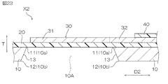
本発明の配線回路基板の第1の実施形態としての配線回路基板X1は、図1から図4に示すように、金属支持基板10と、ベース絶縁層としての絶縁層20と、導体層30と、カバー絶縁層としての絶縁層40とを、厚さ方向Tの一方側に向かってこの順で備える。配線回路基板X1は、厚さ方向Tと直交する方向(面方向)に広がり、所定の平面視形状を有する。 As shown in FIGS. 1 to 4, a wired circuit board X1 as a first embodiment of the wired circuit board of the present invention includes a metal supporting board 10, an insulating layer 20 as a base insulating layer, and a conductor layer 30. , and an insulating layer 40 as an insulating cover layer in this order toward one side in the thickness direction T. As shown in FIG. The printed circuit board X1 extends in a direction (plane direction) orthogonal to the thickness direction T and has a predetermined plan view shape.

金属支持基板10は、配線回路基板X1の強度を確保するための基材である。金属支持基板10の材料としては、例えば、ステンレス鋼、銅、銅合金、アルミニウム、ニッケル、チタン、および42アロイが挙げられる。ステンレス鋼としては、例えば、AISI(米国鉄鋼協会)の規格に基づくSUS304が挙げられる。金属支持基板10の強度の観点から、金属支持基板10は、好ましくは、ステンレス鋼、銅合金、アルミニウム、ニッケル、およびチタンからなる群より選択される少なくとも一種を含み、より好ましくは、ステンレス鋼、銅合金、アルミニウム、ニッケル、およびチタンからなる群より選択される少なくとも一種からなる。金属支持基板10の強度と導電性との両立の観点から、金属支持基板10は、好ましくは銅合金よりなる。 The metal supporting board 10 is a base material for ensuring the strength of the printed circuit board X1. Materials for the metal support substrate 10 include, for example, stainless steel, copper, copper alloys, aluminum, nickel, titanium, and 42 alloy. Examples of stainless steel include SUS304 based on AISI (American Iron and Steel Institute) standards. From the viewpoint of the strength of the metal supporting substrate 10, the metal supporting substrate 10 preferably contains at least one selected from the group consisting of stainless steel, copper alloy, aluminum, nickel, and titanium, more preferably stainless steel, It consists of at least one selected from the group consisting of copper alloys, aluminum, nickel, and titanium. From the viewpoint of compatibility between strength and conductivity of the metal supporting board 10, the metal supporting board 10 is preferably made of a copper alloy.

金属支持基板10は、複数の開口部10Aを有する。複数の開口部10Aのそれぞれは、後記の複数の端子部31のそれぞれに対応して形成されている。開口部10Aについて、詳しくは後述する。 The metal support board 10 has a plurality of openings 10A. Each of the plurality of openings 10A is formed corresponding to each of a plurality of terminal portions 31 described later. Details of the opening 10A will be described later.

金属支持基板10の厚さは、好ましくは20μm以上、より好ましくは30μm以上、更に好ましくは40μm以上、殊更に好ましくは50μm以上、特に好ましくは60μm以上である。このような構成は、金属支持基板10の強度を確保する観点から好ましい。また、金属支持基板10の厚さは、好ましくは250μm以下、より好ましくは200μm以下である。このような構成は、金属支持基板10の柔軟性を確保する観点から好ましい。 The thickness of the metal supporting substrate 10 is preferably 20 μm or more, more preferably 30 μm or more, still more preferably 40 μm or more, even more preferably 50 μm or more, and particularly preferably 60 μm or more. Such a configuration is preferable from the viewpoint of ensuring the strength of the metal supporting board 10 . Also, the thickness of the metal supporting substrate 10 is preferably 250 μm or less, more preferably 200 μm or less. Such a configuration is preferable from the viewpoint of ensuring the flexibility of the metal supporting board 10 .

絶縁層20は、金属支持基板10における厚さ方向Tの一方側に配置されている。本実施形態では、絶縁層20は、金属支持基板10における厚さ方向Tの一方面上に配置されている。絶縁層20の材料としては、例えば、ポリイミド、ポリエーテルニトリル、ポリエーテルスルホン、ポリエチレンテレフタレート、ポリエチレンナフタレート、およびポリ塩化ビニルなどの樹脂材料が挙げられる(後述の絶縁層40の材料としても、同様の樹脂材料が挙げられる)。絶縁層20の厚さは、好ましくは1μm以上、より好ましくは3μm以上であり、また、好ましくは35μm以下、より好ましくは20μm以下である。 The insulating layer 20 is arranged on one side in the thickness direction T of the metal supporting board 10 . In this embodiment, the insulating layer 20 is arranged on one surface in the thickness direction T of the metal supporting board 10 . Examples of the material of the insulating layer 20 include resin materials such as polyimide, polyethernitrile, polyethersulfone, polyethylene terephthalate, polyethylene naphthalate, and polyvinyl chloride (same as the material of the insulating layer 40 described later). resin materials). The thickness of the insulating layer 20 is preferably 1 μm or more, more preferably 3 μm or more, and preferably 35 μm or less, more preferably 20 μm or less.

導体層30は、金属支持基板10における厚さ方向Tの一方側に配置されている。本実施形態では、導体層30は、金属支持基板10における厚さ方向Tの一方面上に配置されている。導体層30の材料としては、例えば、銅、ニッケル、金、およびこれらの合金が挙げられ、好ましくは銅が用いられる。導体層30の厚さは、例えば1μm以上であり、好ましくは3μm以上である。導体層30の厚さは、例えば50μm以下であり、好ましくは30μm以下である。 The conductor layer 30 is arranged on one side in the thickness direction T of the metal supporting board 10 . In this embodiment, the conductor layer 30 is arranged on one surface in the thickness direction T of the metal supporting substrate 10 . Examples of the material of the conductor layer 30 include copper, nickel, gold, and alloys thereof, preferably copper. The thickness of the conductor layer 30 is, for example, 1 μm or more, preferably 3 μm or more. The thickness of the conductor layer 30 is, for example, 50 μm or less, preferably 30 μm or less.

導体層30は、複数の端子部31と、複数の配線部32とを含む。三つの端子部31が第1方向D1に離隔して一列に並び、且つ、端子部31における第2方向D2(第1方向D1と直交する)の一方側から配線部32が延出している場合を、例示的に図示する。 Conductive layer 30 includes a plurality of terminal portions 31 and a plurality of wiring portions 32 . When the three terminal portions 31 are arranged in a row in the first direction D1, and the wiring portions 32 extend from one side of the terminal portions 31 in the second direction D2 (perpendicular to the first direction D1) are exemplarily illustrated.

端子部31の平面視形状としては、例えば、円形、四角形、および角丸四角形が挙げられる。四角形としては正方形および長方形が挙げられる。角丸四角形としては、角丸正方形および角丸長方形が挙げられる(端子部31の平面視形状が角丸長方形である場合を例示的に図示する)。端子部31について図2に示す長さL1(端子部31の第1方向D1の長さ)は、例えば10~1000μmである。端子部31について図2に示す長さL2(端子部31の第2方向D2の長さ)は、例えば10~1000μmである。 Examples of the planar shape of the terminal portion 31 include a circle, a square, and a square with rounded corners. Quadrilaterals include squares and rectangles. As the rounded rectangle, a rounded square and a rounded rectangle are exemplified (the case where the planar view shape of the terminal portion 31 is a rounded rectangle is illustrated as an example). The length L1 of the terminal portion 31 shown in FIG. 2 (the length of the terminal portion 31 in the first direction D1) is, for example, 10 to 1000 μm. The length L2 of the terminal portion 31 shown in FIG. 2 (the length of the terminal portion 31 in the second direction D2) is, for example, 10 to 1000 μm.

配線部32は、絶縁層20上において所定のパターン形状(図示略)を有する。配線部32の一端は、一の端子部31と接続している(図1および図2では、配線部32において後述の絶縁層40で覆われた部分を破線で示す)。当該配線部32の他端は、例えば、図外の他の端子部31と接続している。配線部32の幅(配線部32の延び方向と直交する方向の寸法)は、例えば5μm以上、好ましくは8μm以上であり、また、例えば100μm以下、好ましくは50μm以下である。 The wiring part 32 has a predetermined pattern shape (not shown) on the insulating layer 20 . One end of the wiring portion 32 is connected to one terminal portion 31 (in FIGS. 1 and 2, a portion of the wiring portion 32 covered with an insulating layer 40 described later is indicated by a dashed line). The other end of the wiring portion 32 is connected to, for example, another terminal portion 31 (not shown). The width of the wiring portion 32 (the dimension in the direction orthogonal to the extending direction of the wiring portion 32) is, for example, 5 μm or more, preferably 8 μm or more, and is, for example, 100 μm or less, preferably 50 μm or less.

絶縁層40は、絶縁層20の厚さ方向Tの一方側において導体層30の一部を覆うように配置されている。本実施形態では、絶縁層40は、配線部32の一部を覆うように絶縁層20の厚さ方向Tの一方面上に配置されている。絶縁層20上または配線部32上での絶縁層40の厚さは、好ましくは2μm以上、より好ましくは4μm以上であり、また、好ましくは60μm以下、より好ましくは40μm以下である。 The insulating layer 40 is arranged so as to partially cover the conductor layer 30 on one side of the insulating layer 20 in the thickness direction T. As shown in FIG. In the present embodiment, the insulating layer 40 is arranged on one surface in the thickness direction T of the insulating layer 20 so as to partially cover the wiring portion 32 . The thickness of the insulating layer 40 on the insulating layer 20 or on the wiring portion 32 is preferably 2 μm or more, more preferably 4 μm or more, and preferably 60 μm or less, more preferably 40 μm or less.

金属支持基板10において、開口部10Aは、金属支持基板10を厚さ方向Tに貫通する。開口部10Aは、絶縁層20を介して一の端子部31に対向する。開口部10Aの平面視形状としては、例えば、円形、四角形、および角丸四角形が挙げられる。四角形としては正方形および長方形が挙げられる(開口部10Aの平面視形状が長方形である場合を例示的に図示する)。角丸四角形としては、角丸正方形および角丸長方形が挙げられる。開口部10Aは、好ましくは、端子部31と略同一の平面視形状を有する。 In the metal supporting board 10, the opening 10A penetrates through the metal supporting board 10 in the thickness direction T. As shown in FIG. The opening 10A faces one terminal 31 with the insulating layer 20 interposed therebetween. Examples of the shape of the opening 10A in plan view include a circle, a square, and a square with rounded corners. A quadrangle includes a square and a rectangle (the case where the planar view shape of the opening 10A is a rectangle is illustrated as an example). Rounded squares include rounded squares and rounded rectangles. The opening 10A preferably has substantially the same planar shape as the terminal 31 .

開口部10Aは、厚さ方向Tの一方側の第1開口周端縁11と、厚さ方向Tの他方側の第2開口周端縁12と、第1開口周端縁11および第2開口周端縁12の間の内壁面13とを有する。図3および図4に示すように、第1開口周端縁11は、開口部10Aにおける厚さ方向Tの一方側(絶縁層20側)の第1開口端10aを規定する。また、第2開口周端縁12は、開口部10Aにおける厚さ方向Tの他方側の第2開口端10bを規定する。 The opening 10A includes a first opening peripheral edge 11 on one side in the thickness direction T, a second opening peripheral edge 12 on the other side in the thickness direction T, the first opening peripheral edge 11 and the second opening. and an inner wall surface 13 between peripheral edges 12 . As shown in FIGS. 3 and 4, the first opening peripheral edge 11 defines a first opening end 10a on one side (insulating layer 20 side) in the thickness direction T of the opening 10A. In addition, the second opening peripheral edge 12 defines a second opening end 10b on the other side in the thickness direction T of the opening 10A.

図2に示すように、厚さ方向Tの投影視において、第2開口周端縁12は、第1開口周端縁11の外側に配置されて当該第1開口周端縁11に沿って延びる。開口部10Aにおいて、第1開口端10aの開口面積は相対的に小さく、第2開口端10bの開口面積は相対的に大きい。本実施形態では、図3および図4に示すように、第1開口周端縁11から第2開口周端縁12にかけて開口部10Aの横断面積が次第に増加するように、内壁面13は傾斜している。また、上記投影視における第1開口周端縁11と第2開口周端縁12との間の離隔距離d1(図2に示す)は、好ましくは20μm以上、より好ましくは30μm以上、更に好ましくは40μm以上である。離隔距離d1は、好ましくは120μm以下、より好ましくは110μm以下、更に好ましくは100μm以下である。 As shown in FIG. 2, in a projection view in the thickness direction T, the second opening peripheral edge 12 is arranged outside the first opening peripheral edge 11 and extends along the first opening peripheral edge 11. . In the opening 10A, the opening area of the first opening end 10a is relatively small, and the opening area of the second opening end 10b is relatively large. In this embodiment, as shown in FIGS. 3 and 4, the inner wall surface 13 is inclined so that the cross-sectional area of the opening 10A gradually increases from the first opening peripheral edge 11 to the second opening peripheral edge 12. ing. Further, the separation distance d1 (shown in FIG. 2) between the first opening peripheral edge 11 and the second opening peripheral edge 12 in the projection view is preferably 20 μm or more, more preferably 30 μm or more, and even more preferably 40 μm or more. The separation distance d1 is preferably 120 μm or less, more preferably 110 μm or less, even more preferably 100 μm or less.

本実施形態では、厚さ方向Tの投影視において、第1開口周端縁11の全部が端子部31の内側に配置され、且つ、第2開口周端縁12の全部が端子部31の内側に配置されている。このような構成は、金属支持基板10による端子部31の支持強度を確保する観点から好ましい。 In this embodiment, in the projection view in the thickness direction T, the entire first opening peripheral edge 11 is arranged inside the terminal portion 31, and the entire second opening peripheral edge 12 is located inside the terminal portion 31. are placed in Such a configuration is preferable from the viewpoint of securing the supporting strength of the terminal portion 31 by the metal supporting board 10 .

本実施形態では、上記投影視における端子部31の端縁と第1開口周端縁11との間の離隔距離d2(図2に示す)は、好ましくは5μm以上、より好ましくは10μm以上である。離隔距離d2は、好ましくは400μm以下、より好ましくは300μm以下である。端子部31の長さL1に対する、第1開口端10aの図2に示す長さL3(第1方向D1の長さ)の比率は、好ましくは0.3以上0.98以下である。端子部31の長さL2に対する、第1開口端10aの図2に示す長さL4(第2方向D2の長さ)の比率は、好ましくは0.3以上0.98以下である。長さL1に対する、第2開口端10bの図2に示す長さL5(第1方向D1の長さ)の比率は、好ましくは0.31以上0.99以下である。長さL2に対する、第2開口端10bの図2に示す長さL6(第2方向D2の長さ)の比率は、好ましくは0.31以上0.99以下である。 In the present embodiment, the separation distance d2 (shown in FIG. 2) between the edge of the terminal portion 31 and the peripheral edge 11 of the first opening in the projection view is preferably 5 μm or more, more preferably 10 μm or more. . The separation distance d2 is preferably 400 μm or less, more preferably 300 μm or less. The ratio of the length L3 (the length in the first direction D1) of the first opening end 10a shown in FIG. 2 to the length L1 of the terminal portion 31 is preferably 0.3 or more and 0.98 or less. The ratio of the length L4 (the length in the second direction D2) of the first opening end 10a shown in FIG. 2 to the length L2 of the terminal portion 31 is preferably 0.3 or more and 0.98 or less. The ratio of the length L5 (the length in the first direction D1) of the second open end 10b shown in FIG. 2 to the length L1 is preferably 0.31 or more and 0.99 or less. The ratio of the length L6 (the length in the second direction D2) shown in FIG. 2 of the second opening end 10b to the length L2 is preferably 0.31 or more and 0.99 or less.

図5Aから図5Dは、配線回路基板X1の製造方法の一例を表す。図5Aから図5Dは、本製造方法を、図2に相当する断面の変化として表す。 5A to 5D show an example of a method for manufacturing the printed circuit board X1. 5A to 5D represent the manufacturing method as a cross-sectional variation corresponding to FIG.

本製造方法では、まず、図5Aに示すように、金属支持基板10の厚さ方向Tの一方面上に絶縁層20を形成する(ベース絶縁層形成工程)。本工程では、例えば次のようにして、絶縁層20を形成する。まず、金属支持基板10上に、感光性樹脂の溶液(ワニス)を塗布して塗膜を形成する。次に、この塗膜を加熱によって乾燥させる。次に、塗膜に対して、所定のマスクを介しての露光処理と、その後の現像処理と、その後に必要に応じてベイク処理とを施す。例えば以上のようにして、金属支持基板10上に絶縁層20を形成できる。 In this manufacturing method, first, as shown in FIG. 5A, the insulating layer 20 is formed on one surface of the metal supporting substrate 10 in the thickness direction T (base insulating layer forming step). In this step, the insulating layer 20 is formed, for example, as follows. First, a coating film is formed by coating a solution (varnish) of a photosensitive resin on the metal supporting substrate 10 . The coating is then dried by heating. Next, the coating film is subjected to exposure processing through a predetermined mask, development processing after that, and baking processing if necessary. For example, the insulating layer 20 can be formed on the metal supporting substrate 10 as described above.

次に、図5Bに示すように、絶縁層20上に導体層30を形成する(導体層形成工程)。本工程では、まず、絶縁層20上に、例えばスパッタリング法により、シード層(図示略)を形成する。シード層の材料としては、例えば、Cr、Cu、Ni、Ti、およびこれらの合金が挙げられる。シード層は、単層構造を有してもよく、2層以上の多層構造を有してもよい。シード層が多層構造を有する場合、当該シード層は、例えば、下層としてのクロム層と、当該クロム層上の銅層とからなる。次に、シード層上にレジストパターンを形成する。レジストパターンは、導体層30のパターン形状に相当する形状の開口部を有する。レジストパターンの形成においては、例えば、感光性のレジストフィルムをシード層上に貼り合わせてレジスト膜を形成した後、当該レジスト膜に対し、所定マスクを介しての露光処理と、その後の現像処理と、その後に必要に応じてベイク処理とを施す。導体層30の形成においては、次に、例えば電解メッキ法により、レジストパターンの開口部内のシード層上に上記した金属を成長させる。次に、レジストパターンをエッチングにより除去する。次に、シード層においてレジストパターン除去によって露出した部分を、エッチングにより除去する。例えば以上のようにして、所定パターンの導体層30(端子部31,配線部32)を形成できる。 Next, as shown in FIG. 5B, a conductor layer 30 is formed on the insulating layer 20 (conductor layer forming step). In this step, first, a seed layer (not shown) is formed on the insulating layer 20 by sputtering, for example. Examples of seed layer materials include Cr, Cu, Ni, Ti, and alloys thereof. The seed layer may have a single layer structure or a multilayer structure of two or more layers. When the seed layer has a multi-layer structure, the seed layer consists of, for example, a chromium layer as a lower layer and a copper layer on the chromium layer. Next, a resist pattern is formed on the seed layer. The resist pattern has an opening with a shape corresponding to the pattern shape of the conductor layer 30 . In forming a resist pattern, for example, after a photosensitive resist film is laminated on a seed layer to form a resist film, the resist film is exposed through a predetermined mask and then developed. , and then baking if necessary. In forming the conductor layer 30, the above-described metal is then grown on the seed layer in the openings of the resist pattern by, for example, electroplating. Next, the resist pattern is removed by etching. Next, the portion of the seed layer exposed by removing the resist pattern is removed by etching. For example, the conductor layer 30 (the terminal portion 31 and the wiring portion 32) having a predetermined pattern can be formed as described above.

次に、図5Cに示すように、絶縁層20上において、導体層30の一部を覆うように絶縁層40を形成する(カバー絶縁層形成工程)。本工程では、例えば次のようにして、絶縁層40を形成する。まず、絶縁層20上および導体層30上に、感光性樹脂の溶液(ワニス)を塗布して塗膜を形成する。次に、この塗膜を乾燥させる。次に、塗膜に対して、所定のマスクを介しての露光処理と、その後の現像処理と、その後に必要に応じてベイク処理とを施す。例えば以上のようにして、絶縁層40を形成できる。 Next, as shown in FIG. 5C, the insulating layer 40 is formed on the insulating layer 20 so as to partially cover the conductor layer 30 (insulating cover layer forming step). In this step, the insulating layer 40 is formed, for example, as follows. First, a solution of a photosensitive resin (varnish) is applied on the insulating layer 20 and the conductor layer 30 to form a coating film. The coating is then dried. Next, the coating film is subjected to exposure processing through a predetermined mask, development processing after that, and baking processing if necessary. For example, the insulating layer 40 can be formed as described above.

次に、図5Dに示すように、金属支持基板10に開口部10Aを形成する(開口部形成工程)。本工程では、まず、金属支持基板10の厚さ方向Tの他方面上にレジストパターンを形成する。レジストパターンは、上述の開口部10Aの第2開口周端縁12の形状に対応する形状の開口部を有する。レジストパターンの形成においては、例えば、感光性のレジストフィルムを金属支持基板10の前記他方面上に貼り合わせてレジスト膜を形成した後、当該レジスト膜に対し、所定マスクを介しての露光処理と、その後の現像処理と、その後に必要に応じてベイク処理とを施す。開口部10Aの形成においては、次に、レジストパターンをエッチングマスクとして、金属支持基板10に対し、厚さ方向Tの他方側からのウェットエッチングを実施する(エッチング処理)。ウェットエッチングのためのエッチング液としては、例えば、塩化第二鉄水溶液および塩化第二銅溶液が挙げられる。エッチング液の濃度は、例えば30~55質量%である。エッチング液の温度は、例えば20℃~55℃である。エッチングの時間は、例えば1~15分である。 Next, as shown in FIG. 5D, openings 10A are formed in the metal supporting substrate 10 (opening forming step). In this step, first, a resist pattern is formed on the other surface in the thickness direction T of the metal supporting board 10 . The resist pattern has an opening having a shape corresponding to the shape of the second opening peripheral edge 12 of the opening 10A described above. In forming the resist pattern, for example, a photosensitive resist film is laminated on the other surface of the metal supporting substrate 10 to form a resist film, and then the resist film is exposed through a predetermined mask. , subsequent development processing, and then baking processing as required. In forming the opening 10A, next, wet etching is performed on the metal supporting board 10 from the other side in the thickness direction T using the resist pattern as an etching mask (etching process). Etching solutions for wet etching include, for example, ferric chloride aqueous solutions and cupric chloride solutions. The concentration of the etchant is, for example, 30-55 mass %. The temperature of the etchant is, for example, 20.degree. C. to 55.degree. The etching time is, for example, 1 to 15 minutes.

本工程では、必要に応じて、上記エッチング処理により、金属支持基板10における開口部10Aの形成と外形加工とを同時的に実施する。 In this step, the formation of the opening 10A in the metal supporting substrate 10 and the outer shape processing are simultaneously performed by the above-described etching process, if necessary.

以上のようにして、配線回路基板X1を製造できる。 As described above, the printed circuit board X1 can be manufactured.

配線回路基板X1においては、上述のように、絶縁層20を介して端子部31に対向する開口部10Aが金属支持基板10に形成されている。このような構成は、端子部31の特性インピーダンスを調整するのに適する。加えて、配線回路基板X1の厚さ方向Tの投影視において、開口部10Aの第2開口周端縁12は、第1開口周端縁11の外側に配置されて当該第1開口周端縁11に沿って延びる。すなわち、開口部10Aにおいて、厚さ方向Tの一方側(端子部側)の端部の第1開口面積は相対的に小さく、厚さ方向Tの他方側の端部の第2開口面積は相対的に大きい。このような構成は、金属支持基板10による端子部31の支持強度の低下を抑制しつつ、開口部10Aの開口スペースを広く確保して端子部31の特性インピーダンスを調整するのに適する。したがって、配線回路基板X1は、端子部13に対する支持強度を確保しつつ端子部31の特性インピーダンスを調整するのに適する。このような技術的効果は、後述の変形例および第2の実施形態においても得られる。 In the wired circuit board X1, the metal supporting board 10 is formed with the opening 10A facing the terminal 31 with the insulating layer 20 interposed therebetween, as described above. Such a configuration is suitable for adjusting the characteristic impedance of the terminal portion 31 . In addition, in the projection view of the printed circuit board X1 in the thickness direction T, the second opening peripheral edge 12 of the opening 10A is arranged outside the first opening peripheral edge 11 and is located outside the first opening peripheral edge 11. 11 extending along. That is, in the opening 10A, the first opening area at the end on one side (terminal side) in the thickness direction T is relatively small, and the second opening area at the end on the other side in the thickness direction T is relatively small. relatively large. Such a configuration is suitable for adjusting the characteristic impedance of the terminal portion 31 by securing a wide opening space for the opening portion 10A while suppressing a decrease in supporting strength of the terminal portion 31 by the metal supporting board 10 . Therefore, the printed circuit board X1 is suitable for adjusting the characteristic impedance of the terminal portion 31 while securing the supporting strength for the terminal portion 13 . Such technical effects are also obtained in the modified example and the second embodiment, which will be described later.

配線回路基板X1においては、図2および図3に示すように、配線部32において端子部31と接続している端部32aが、厚さ方向Tの投影視において、開口部10Aの第1開口端10a上に位置せず、金属支持基板10上に位置する。このような構成は、配線回路基板X1に対する外部部品(図示略)の実装工程において、端子部31に対して外部部品の端子を接合する時に配線部31の端部32aが折れるのを防止するのに適する。このような技術的効果は、図8から図10に示す後述の変形例、図14から図16に示す後述の変形例、図17に示す後述の変形例、図18に示す後述の変形例、図25から図27に示す後述の変形例、図28に示す後述の変形例、および、図29に示す後述の変形例においても、得られる。 In the wired circuit board X1, as shown in FIGS. 2 and 3, the end portion 32a of the wiring portion 32 connected to the terminal portion 31 is the first opening of the opening portion 10A in the projection view in the thickness direction T. It is not located on the edge 10a, but on the metal support substrate 10. FIG. Such a configuration prevents the end portion 32a of the wiring portion 31 from breaking when connecting the terminal of the external component to the terminal portion 31 in the process of mounting the external component (not shown) on the printed circuit board X1. Suitable for Such a technical effect is achieved by a modification shown in FIGS. 8 to 10, a modification shown in FIGS. 14 to 16, a modification shown in FIG. 17, a modification shown in FIG. 25 to 27, a modified example shown in FIG. 28, and a modified example shown in FIG. 29, which will be described later.

配線回路基板X1の金属支持基板10において、開口部10Aは、図6に示すように、縦断面視において外側に膨らむ形状を有してもよい。すなわち、開口部10Aの内壁面13は、外側に湾曲する湾曲壁面(湾曲面)であってもよい(当該湾曲面の曲率中心は、開口部10A内に位置する)。このような構成は、開口部10Aの第1開口端10aの面積を抑えつつ、開口部10Aの開口スペースを広く確保するのに適する。 In the metal supporting board 10 of the printed circuit board X1, the opening 10A may have a shape that bulges outward in a vertical cross-sectional view, as shown in FIG. That is, the inner wall surface 13 of the opening 10A may be a curved wall surface (curved surface) that curves outward (the center of curvature of the curved surface is located within the opening 10A). Such a configuration is suitable for securing a wide opening space for the opening 10A while suppressing the area of the first opening end 10a of the opening 10A.

このような開口部10Aを形成するには、図5Dを参照して上述したウェットエッチングにおいて、エッチング液として好ましくは塩化第二鉄水溶液を用いる。エッチング液の濃度は、好ましくは30質量%以上、より好ましくは32質量%以上である。エッチング液の濃度は、好ましくは55質量%以下、より好ましくは53質量%以下である。エッチング液の濃度が低いほど、厚さ方向Tの投影視における第1開口周端縁11と第2開口周端縁12との間の上記離隔距離d1を広げやすい。エッチング液の温度は、好ましくは20℃以上、より好ましくは25℃以上、更に好ましくは好ましくは30℃以上である。エッチング液の温度は、好ましくは80℃以下、より好ましくは75℃以下である。エッチング液の温度が高いほど、内壁面13を湾曲させやすい(内壁面13の曲率半径を小さくしやすい)。エッチングの時間は、好ましくは1分以上、より好ましくは2分以上である。エッチングの時間は、好ましくは15分以下、より好ましくは12分以下である。 In order to form such an opening 10A, an aqueous solution of ferric chloride is preferably used as an etchant in the wet etching described above with reference to FIG. 5D. The concentration of the etchant is preferably 30% by mass or more, more preferably 32% by mass or more. The concentration of the etchant is preferably 55% by mass or less, more preferably 53% by mass or less. The lower the concentration of the etchant, the easier it is to widen the separation distance d1 between the first opening peripheral edge 11 and the second opening peripheral edge 12 in the projection view in the thickness direction T. The temperature of the etchant is preferably 20° C. or higher, more preferably 25° C. or higher, and even more preferably 30° C. or higher. The temperature of the etchant is preferably 80° C. or lower, more preferably 75° C. or lower. The higher the temperature of the etchant, the easier it is to bend the inner wall surface 13 (the easier it is to reduce the radius of curvature of the inner wall surface 13). The etching time is preferably 1 minute or longer, more preferably 2 minutes or longer. The etching time is preferably 15 minutes or less, more preferably 12 minutes or less.

配線回路基板X1における端子部31は、図7に示すように、2層構造を有してもよい。図7に示す端子部31は、具体的には、絶縁層20側の第1導体層31Aと、当該第1導体層31A上の第2導体層31Bとを含む。 The terminal portion 31 in the printed circuit board X1 may have a two-layer structure as shown in FIG. Specifically, the terminal portion 31 shown in FIG. 7 includes a first conductor layer 31A on the insulating layer 20 side and a second conductor layer 31B on the first conductor layer 31A.

第1導体層31Aは、図1から図4を参照して上述した端子部31と同じである。第2導体層31Bは、平面視において、第1導体層31Aの外郭形状以内に収まる外郭形状を有する。第2導体層31Bの厚さは、例えば1μm以上であり、好ましくは3μm以上である。第2導体層31Bの厚さは、例えば50μm以下であり、好ましくは30μm以下である。第2導体層31Bの材料としては、導体層30に関して上記した材料が挙げられる。第1導体層31Aの材料と第2導体層31Bの材料は、好ましくは同一であり、より好ましくは銅である。第1導体層31Aの材料と第2導体層31Bの材料は、異なってもよい。 31 A of 1st conductor layers are the same as the terminal part 31 mentioned above with reference to FIGS. 1-4. The second conductor layer 31B has an outline shape that fits within the outline shape of the first conductor layer 31A in plan view. The thickness of the second conductor layer 31B is, for example, 1 μm or more, preferably 3 μm or more. The thickness of the second conductor layer 31B is, for example, 50 μm or less, preferably 30 μm or less. As the material for the second conductor layer 31B, the materials described above for the conductor layer 30 can be used. The material of the first conductor layer 31A and the material of the second conductor layer 31B are preferably the same, more preferably copper. The material of the first conductor layer 31A and the material of the second conductor layer 31B may be different.

図7に示す端子部31を備える配線回路基板X1は、例えば、導体層形成工程(図5B)とカバー絶縁層形成工程(図5C)との間において導体層30上に第2導体層31Bをパターン形成すること以外は、配線回路基板X1の上述の製造方法と同様の方法で、製造できる。 The wired circuit board X1 having the terminal portion 31 shown in FIG. 7 has a second conductor layer 31B formed on the conductor layer 30 between the conductor layer forming step (FIG. 5B) and the cover insulating layer forming step (FIG. 5C), for example. Except for the pattern formation, the printed circuit board X1 can be manufactured by the same method as described above.

端子部31が2層構造を有することは、端子部31の強度の確保の観点から好ましい。端子部31がこのような2層構造を有してもよいことは、後述の変形例および第2の実施形態においても同様である。 It is preferable from the viewpoint of ensuring the strength of the terminal portion 31 that the terminal portion 31 has a two-layer structure. The fact that the terminal portion 31 may have such a two-layer structure is the same in a modified example and a second embodiment which will be described later.

配線回路基板X1では、図8から図10に示すように、厚さ方向Tの投影視において、開口部10Aの第1開口周端縁11の全部が端子部31の内側に配置され、且つ、第2開口周端縁12の全部が端子部31の外側に配置されてもよい。このような構成は、開口部10Aの開口スペースを広く確保する観点から好ましい。 In the printed circuit board X1, as shown in FIGS. 8 to 10, the entire first opening peripheral edge 11 of the opening 10A is arranged inside the terminal portion 31 in the projection view in the thickness direction T, and The entire second opening peripheral edge 12 may be arranged outside the terminal portion 31 . Such a configuration is preferable from the viewpoint of securing a wide opening space for the opening 10A.

本変形例において、端子部31の長さL1に対する、第1開口端10aの図8に示す長さL3の比率は、好ましくは0.4以上0.98以下である。端子部31の長さL2に対する、第1開口端10aの図8に示す長さL4の比率は、好ましくは0.4以上0.98以下である。長さL1に対する、第2開口端10bの図8に示す長さL5の比率は、好ましくは1.01以上3以下である。長さL2に対する、第2開口端10bの図8に示す長さL6の比率は、好ましくは1.01以上3以下である。 In this modification, the ratio of the length L3 of the first opening end 10a shown in FIG. 8 to the length L1 of the terminal portion 31 is preferably 0.4 or more and 0.98 or less. The ratio of the length L4 of the first opening end 10a shown in FIG. 8 to the length L2 of the terminal portion 31 is preferably 0.4 or more and 0.98 or less. The ratio of the length L5 shown in FIG. 8 of the second open end 10b to the length L1 is preferably 1.01 or more and 3 or less. The ratio of the length L6 of the second open end 10b shown in FIG. 8 to the length L2 is preferably 1.01 or more and 3 or less.

配線回路基板X1では、図11から図13に示すように、厚さ方向Tの投影視において、開口部10Aにおける第1開口周端縁11の全部および第2開口周端縁12の全部が端子部31の外側に配置されてもよい。このような構成は、開口部10Aの開口スペースを広く確保する観点から好ましい。 In the printed circuit board X1, as shown in FIGS. 11 to 13, in the projection view in the thickness direction T, the entire first opening peripheral edge 11 and the entire second opening peripheral edge 12 of the opening 10A are terminals. It may be arranged outside the portion 31 . Such a configuration is preferable from the viewpoint of securing a wide opening space for the opening 10A.

本変形例において、上記投影視における端子部31の端縁と第1開口周端縁11との間の離隔距離d2(図11に示す)は、好ましくは5μm以上、より好ましくは10μm以上である。離隔距離d2は、好ましくは400μm以下、より好ましくは300μm以下である。端子部31の長さL1に対する、第1開口端10aの図11に示す長さL3の比率は、好ましくは1.01以上4以下である。端子部31の長さL2に対する、第1開口端10aの図11に示す長さL4の比率は、好ましくは1.01以上4以下である。長さL1に対する、第2開口端10bの図11に示す長さL5の比率は、好ましくは1.05以上5以下である。長さL2に対する、第2開口端10bの図11に示す長さL6の比率は、好ましくは1.05以上5以下である。 In this modification, the separation distance d2 (shown in FIG. 11) between the edge of the terminal portion 31 and the peripheral edge 11 of the first opening in the projection view is preferably 5 μm or more, more preferably 10 μm or more. . The separation distance d2 is preferably 400 μm or less, more preferably 300 μm or less. The ratio of the length L3 of the first opening end 10a shown in FIG. 11 to the length L1 of the terminal portion 31 is preferably 1.01 or more and 4 or less. The ratio of the length L4 of the first opening end 10a shown in FIG. 11 to the length L2 of the terminal portion 31 is preferably 1.01 or more and 4 or less. The ratio of the length L5 of the second open end 10b shown in FIG. 11 to the length L1 is preferably 1.05 or more and 5 or less. The ratio of the length L6 of the second open end 10b shown in FIG. 11 to the length L2 is preferably 1.05 or more and 5 or less.

配線回路基板X1では、図14から図16に示すように、開口部10Aの第1開口周端縁11が、部分11a(第1部分)と部分11b(第2部分)とを含んでもよい。厚さ方向Tの投影視において、部分11aは、端子部31の内側に配置され、部分11bは、端子部31の外側に配置されている。部分11aは、第1方向D1に延びる。部分11bは、第2方向D2に延びる部分と、第1方向D1に延びる部分とを含む。厚さ方向Tの投影視において、第2開口周端縁12は、端子部31の内側に配置されて部分11aに沿って延びる部分12a(第3部分)と、端子部31の外側に配置されて部分11bに沿って延びる部分12bとを含む。第2開口周端縁12は、端子部31の外側に配置されて部分11aに沿って延びる部分12a(第4部分)と、端子部31の外側に配置されて部分11bに沿って延びる部分12bとを含んでもよい。これら構成は、金属支持基板10による端子部31の支持強度の確保と、開口部10Aの開口スペースの確保との両立の観点から、好ましい。 In the printed circuit board X1, as shown in FIGS. 14 to 16, the first opening peripheral edge 11 of the opening 10A may include a portion 11a (first portion) and a portion 11b (second portion). In a projection view in the thickness direction T, the portion 11 a is arranged inside the terminal portion 31 and the portion 11 b is arranged outside the terminal portion 31 . The portion 11a extends in the first direction D1. The portion 11b includes a portion extending in the second direction D2 and a portion extending in the first direction D1. In a projection view in the thickness direction T, the second opening peripheral edge 12 has a portion 12a (third portion) arranged inside the terminal portion 31 and extending along the portion 11a, and a portion 12a (third portion) arranged outside the terminal portion 31. and a portion 12b extending along and along portion 11b. The second opening peripheral edge 12 has a portion 12a (fourth portion) arranged outside the terminal portion 31 and extending along the portion 11a, and a portion 12b arranged outside the terminal portion 31 and extending along the portion 11b. and may include These configurations are preferable from the viewpoint of ensuring both the support strength of the terminal portion 31 by the metal supporting board 10 and the opening space of the opening portion 10A.

本変形例において、上記投影視における端子部31の端縁と部分11aとの間の離隔距離d3(図14に示す)は、好ましくは5μm以上、より好ましくは10μm以上である。離隔距離d3は、好ましくは400μm以下、より好ましくは300μm以下である。上記投影視における端子部31の端縁と部分11bとの間の離隔距離d4(図14に示す)は、好ましくは5μm以上、より好ましくは10μm以上である。離隔距離d4は、好ましくは400μm以下、より好ましくは300μm以下である。端子部31の長さL1に対する、第1開口端10aの図14に示す長さL3の比率は、好ましくは1.01以上4以下である。端子部31の長さL2に対する、第1開口端10aの図14に示す長さL4の比率は、好ましくは0.31以上0.99以下である。長さL1に対する、第2開口端10bの図14に示す長さL5の比率は、好ましくは1.05以上5以下である。長さL2に対する、第2開口端10bの図14に示す長さL6の比率は、好ましくは0.31以上0.99以下である。 In this modification, the separation distance d3 (shown in FIG. 14) between the edge of the terminal portion 31 and the portion 11a in the projection view is preferably 5 μm or more, more preferably 10 μm or more. The separation distance d3 is preferably 400 μm or less, more preferably 300 μm or less. A separation distance d4 (shown in FIG. 14) between the edge of the terminal portion 31 and the portion 11b in the projection view is preferably 5 μm or more, more preferably 10 μm or more. The separation distance d4 is preferably 400 μm or less, more preferably 300 μm or less. The ratio of the length L3 of the first opening end 10a shown in FIG. 14 to the length L1 of the terminal portion 31 is preferably 1.01 or more and 4 or less. The ratio of the length L4 of the first opening end 10a shown in FIG. 14 to the length L2 of the terminal portion 31 is preferably 0.31 or more and 0.99 or less. The ratio of the length L5 of the second open end 10b shown in FIG. 14 to the length L1 is preferably 1.05 or more and 5 or less. The ratio of the length L6 of the second open end 10b shown in FIG. 14 to the length L2 is preferably 0.31 or more and 0.99 or less.

図14から図16に示す上述の変形例では、図17に示すように、端子部31における配線部32接続側とは反対側の端部31aが、厚さ方向Tの投影視において、開口部10Aの第1開口端10a上に位置してもよい。 14 to 16, as shown in FIG. 17, the end portion 31a of the terminal portion 31 opposite to the wiring portion 32 connection side is an opening in the projection view in the thickness direction T. It may be located on the first open end 10a of 10A.

図17に示す変形例において、端子部31の形成箇所が金属支持基板10の端縁近傍である場合には、図18に示すように、開口部10Aは、面方向に開口していてもよい。 In the modification shown in FIG. 17, when the terminal portion 31 is formed near the edge of the metal supporting substrate 10, the opening portion 10A may open in the plane direction as shown in FIG. .

配線回路基板X1では、図19から図21に示すように、開口部10Aの第1開口周端縁11が、部分11c(第1部分)と部分11d(第2部分)とを含んでもよい。厚さ方向Tの投影視において、部分11cは、端子部31の内側に配置され、部分11dは、端子部31の外側に配置されている。部分11cは、第2方向D2に延びる。部分11dは、第1方向D1に延びる部分と、第2方向D2に延びる部分とを含む。厚さ方向Tの投影視において、第2開口周端縁12は、端子部31の内側に配置されて部分11cに沿って延びる部分12c(第3部分)と、端子部31の外側に配置されて部分11dに沿って延びる部分12dとを含む。第2開口周端縁12は、端子部31の外側に配置されて部分11cに沿って延びる部分12c(第4部分)と、端子部31の外側に配置されて部分11dに沿って延びる部分12dとを含んでもよい。これら構成は、金属支持基板10による端子部31の支持強度の確保と、開口部10Aの開口スペースの確保との両立の観点から、好ましい。 In the printed circuit board X1, as shown in FIGS. 19 to 21, the first opening peripheral edge 11 of the opening 10A may include a portion 11c (first portion) and a portion 11d (second portion). In a projection view in the thickness direction T, the portion 11c is arranged inside the terminal portion 31, and the portion 11d is arranged outside the terminal portion 31. As shown in FIG. The portion 11c extends in the second direction D2. The portion 11d includes a portion extending in the first direction D1 and a portion extending in the second direction D2. In a projection view in the thickness direction T, the second opening peripheral edge 12 has a portion 12c (third portion) arranged inside the terminal portion 31 and extending along the portion 11c, and a portion 12c (third portion) arranged outside the terminal portion 31. and a portion 12d extending along the portion 11d. The second opening peripheral edge 12 has a portion 12c (fourth portion) arranged outside the terminal portion 31 and extending along the portion 11c, and a portion 12d arranged outside the terminal portion 31 and extending along the portion 11d. and may include These configurations are preferable from the viewpoint of ensuring both the support strength of the terminal portion 31 by the metal supporting board 10 and the opening space of the opening portion 10A.

本変形例において、上記投影視における端子部31の端縁と部分11cとの間の離隔距離d5(図19に示す)は、好ましくは5μm以上、より好ましくは10μm以上である。離隔距離d5は、好ましくは400μm以下、より好ましくは300μm以下である。上記投影視における端子部31の端縁と部分11dとの間の離隔距離d6(図19に示す)は、好ましくは5μm以上、より好ましくは10μm以上である。離隔距離d6は、好ましくは400μm以下、より好ましくは300μm以下である。端子部31の長さL1に対する、第1開口端10aの図19に示す長さL3の比率は、好ましくは0.31以上0.99以下である。端子部31の長さL2に対する、第1開口端10aの図19に示す長さL4の比率は、好ましくは1.01以上4以下である。長さL1に対する、第2開口端10bの図19に示す長さL5の比率は、好ましくは0.31以上0.99以下である。長さL2に対する、第2開口端10bの図19に示す長さL6の比率は、好ましくは1.05以上5以下である。 In this modification, the separation distance d5 (shown in FIG. 19) between the edge of the terminal portion 31 and the portion 11c in the projection view is preferably 5 μm or more, more preferably 10 μm or more. The separation distance d5 is preferably 400 μm or less, more preferably 300 μm or less. A separation distance d6 (shown in FIG. 19) between the edge of the terminal portion 31 and the portion 11d in the projection view is preferably 5 μm or more, more preferably 10 μm or more. The separation distance d6 is preferably 400 μm or less, more preferably 300 μm or less. The ratio of the length L3 of the first opening end 10a shown in FIG. 19 to the length L1 of the terminal portion 31 is preferably 0.31 or more and 0.99 or less. The ratio of the length L4 of the first opening end 10a shown in FIG. 19 to the length L2 of the terminal portion 31 is preferably 1.01 or more and 4 or less. The ratio of the length L5 of the second open end 10b shown in FIG. 19 to the length L1 is preferably 0.31 or more and 0.99 or less. The ratio of the length L6 of the second open end 10b shown in FIG. 19 to the length L2 is preferably 1.05 or more and 5 or less.

上述の配線回路基板X1では、端子部31ごとに一の開口部10Aを設けるのに代えて、端子部31ごとに複数の開口部(絶縁層20を介して当該端子部31に対向する)を設けてもよい。このような構成によって端子部31の特性インピーダンスを調整してもよい。 In the wired circuit board X1 described above, instead of providing one opening 10A for each terminal portion 31, a plurality of openings (facing the terminal portion 31 via the insulating layer 20) are provided for each terminal portion 31. may be provided. The characteristic impedance of the terminal portion 31 may be adjusted by such a configuration.

図22から図24は、本発明の配線回路基板の第2の実施形態としての配線回路基板X2を表す。配線回路基板X2は、配線回路基板X1と同様に、金属支持基板10と、ベース絶縁層としての絶縁層20と、導体層30と、カバー絶縁層としての絶縁層40とを、厚さ方向Tの一方側に向かってこの順で備える。配線回路基板X2は、開口部10Aが絶縁層20を介して一の端子部31に対向するのに代えて、一の開口部10Aが絶縁層20を介して複数の端子部31(第1方向D1に離隔して一列に並ぶ)に対向する点で、配線回路基板X1と異なる。このこと以外について、配線回路基板X2は、配線回路基板X1と同じ構成を有する。 22 to 24 show a wired circuit board X2 as a second embodiment of the wired circuit board of the present invention. In the wired circuit board X2, similarly to the wired circuit board X1, the metal supporting board 10, the insulating layer 20 as the base insulating layer, the conductor layer 30, and the insulating layer 40 as the cover insulating layer are arranged in the thickness direction T Prepare in this order towards one side of the In the wired circuit board X2, instead of the opening 10A facing one terminal portion 31 with the insulating layer 20 interposed therebetween, the one opening 10A faces the plurality of terminal portions 31 (first direction) with the insulating layer 20 interposed therebetween. D1 and arranged in a row), unlike the printed circuit board X1. Except for this, the wired circuit board X2 has the same configuration as the wired circuit board X1.

配線回路基板X2における開口部10Aは、図22に示すように、厚さ方向Tの投影視において、第1開口周端縁11の全部および第2開口周端縁12の全部が端子部31の外側に配置されている。このような構成は、開口部10Aの開口スペースを広く確保する観点から好ましい。 As shown in FIG. 22, the opening 10A in the printed circuit board X2 has the entire first peripheral edge 11 and the entire second peripheral edge 12 of the terminal 31 in the projection view in the thickness direction T. placed outside. Such a configuration is preferable from the viewpoint of securing a wide opening space for the opening 10A.

本実施形態では、上記投影視における端子部31の端縁と第1開口周端縁11との間の離隔距離d7は、好ましくは5μm以上、より好ましくは10μm以上である。離隔距離d7は、好ましくは400μm以下、より好ましくは300μm以下である。端子部31の長さL2に対する、第1開口端10aの図22に示す長さL4の比率は、好ましくは1.01以上4以下である。長さL2に対する、第2開口端10bの図22に示す長さL6の比率は、好ましくは1.01以上5以下である。 In this embodiment, the separation distance d7 between the edge of the terminal portion 31 and the peripheral edge 11 of the first opening in the projection view is preferably 5 μm or more, more preferably 10 μm or more. The separation distance d7 is preferably 400 μm or less, more preferably 300 μm or less. The ratio of the length L4 of the first opening end 10a shown in FIG. 22 to the length L2 of the terminal portion 31 is preferably 1.01 or more and 4 or less. The ratio of the length L6 of the second open end 10b shown in FIG. 22 to the length L2 is preferably 1.01 or more and 5 or less.

配線回路基板X2では、図25から図27に示すように、開口部10Aの第1開口周端縁11が、部分11a(第1部分)と部分11b(第2部分)とを含んでもよい。厚さ方向Tの投影視において、部分11aは、端子部31の内側に配置され、部分11bは、端子部31外に配置されている。部分11aは、第1方向D1に延びる。部分11bは、第1方向D1に延びる部分と、第2方向D2に延びる部分とを含む。厚さ方向Tの投影視において、第2開口周端縁12は、端子部31の内側に配置されて部分11aに沿って延びる部分12a(第3部分)と、端子部31の外側に配置されて部分11bに沿って延びる部分12bとを含む。第2開口周端縁12は、端子部31の外側に配置されて部分11aに沿って延びる部分12a(第4部分)と、端子部31の外側に配置されて部分11bに沿って延びる部分12bとを含んでもよい。これら構成は、金属支持基板10による端子部31の支持強度の確保と、開口部10Aの開口スペースの確保との両立の観点から、好ましい。 In the printed circuit board X2, as shown in FIGS. 25 to 27, the first opening peripheral edge 11 of the opening 10A may include a portion 11a (first portion) and a portion 11b (second portion). In a projection view in the thickness direction T, the portion 11 a is arranged inside the terminal portion 31 and the portion 11 b is arranged outside the terminal portion 31 . The portion 11a extends in the first direction D1. The portion 11b includes a portion extending in the first direction D1 and a portion extending in the second direction D2. In a projection view in the thickness direction T, the second opening peripheral edge 12 has a portion 12a (third portion) arranged inside the terminal portion 31 and extending along the portion 11a, and a portion 12a (third portion) arranged outside the terminal portion 31. and a portion 12b extending along and along portion 11b. The second opening peripheral edge 12 has a portion 12a (fourth portion) arranged outside the terminal portion 31 and extending along the portion 11a, and a portion 12b arranged outside the terminal portion 31 and extending along the portion 11b. and may include These configurations are preferable from the viewpoint of ensuring both the support strength of the terminal portion 31 by the metal supporting board 10 and the opening space of the opening portion 10A.

本変形例において、上記投影視における端子部31の端縁と部分11aとの間の離隔距離d8(図25に示す)は、好ましくは5μm以上、より好ましくは10μm以上である。離隔距離d8は、好ましくは400μm以下、より好ましくは300μm以下である。上記投影視における端子部31の端縁と部分11bとの間の離隔距離d9(図25に示す)は、好ましくは5μm以上、より好ましくは10μm以上である。離隔距離d9は、好ましくは400μm以下、より好ましくは300μm以下である。端子部31の長さL2に対する、第1開口端10aの図25に示す長さL4の比率は、好ましくは0.31以上0.99以下である。長さL2に対する、第2開口端10bの図25に示す長さL6の比率は、好ましくは0.31以上0.99以下である。 In this modification, the separation distance d8 (shown in FIG. 25) between the edge of the terminal portion 31 and the portion 11a in the projection view is preferably 5 μm or more, more preferably 10 μm or more. The separation distance d8 is preferably 400 μm or less, more preferably 300 μm or less. A separation distance d9 (shown in FIG. 25) between the edge of the terminal portion 31 and the portion 11b in the projection view is preferably 5 μm or more, more preferably 10 μm or more. The separation distance d9 is preferably 400 μm or less, more preferably 300 μm or less. The ratio of the length L4 of the first opening end 10a shown in FIG. 25 to the length L2 of the terminal portion 31 is preferably 0.31 or more and 0.99 or less. The ratio of the length L6 of the second open end 10b shown in FIG. 25 to the length L2 is preferably 0.31 or more and 0.99 or less.

図25から図27に示す上述の変形例では、図28に示すように、各端子部31における配線部32接続側とは反対側の端部31aが、厚さ方向Tの投影視において、開口部10Aの第1開口端10a上に位置してもよい。 25 to 27, as shown in FIG. 28, the end portion 31a of each terminal portion 31 on the side opposite to the wiring portion 32 connection side is an opening in the projection view in the thickness direction T. It may be located on the first open end 10a of the portion 10A.

図28に示す変形例において、端子部31の形成箇所が金属支持基板10の端縁近傍である場合には、図29に示すように、開口部10Aは、面方向に開口していてもよい。 In the modification shown in FIG. 28, when the terminal portion 31 is formed in the vicinity of the edge of the metal supporting board 10, the opening 10A may open in the plane direction as shown in FIG. .

X1,X2 配線回路基板
T 厚さ方向
10 金属支持基板
10A 開口部
10a 第1開口端
10b 第2開口端
11 第1開口周端縁
12 第2開口周端縁
13 内壁面
20,40 絶縁層
30 導体層
31 端子部
32 配線部
X1, X2 Wiring circuit board T thickness direction 10 metal supporting board 10A opening 10a first opening end 10b second opening end 11 first opening peripheral edge 12 second opening peripheral edge 13 inner wall surfaces 20, 40 insulating layer 30 Conductor layer 31 Terminal portion 32 Wiring portion

Claims (8)

金属支持基板と、絶縁層と、導体層とを、厚さ方向一方側に向かってこの順で備え、
前記導体層が、少なくとも一つの端子部と、当該端子部から延出する配線部とを含み、
前記金属支持基板が、当該金属支持基板を前記厚さ方向に貫通し且つ前記絶縁層を介して前記端子部に対向する開口部を有し、
前記開口部が、前記厚さ方向一方側の第1開口周端縁と、前記厚さ方向他方側の第2開口周端縁とを有し、前記厚さ方向の投影視において、前記第2開口周端縁は、前記第1開口周端縁の外側に配置されて当該第1開口周端縁に沿って延び、
前記投影視において、前記第1開口周端縁の全部が、前記端子部の内側に配置されており、前記第2開口周端縁の全部が、前記端子部の外側に配置されている、配線回路基板。
A metal supporting substrate, an insulating layer, and a conductor layer are provided in this order toward one side in the thickness direction,
The conductor layer includes at least one terminal portion and a wiring portion extending from the terminal portion,
wherein the metal supporting substrate has an opening penetrating through the metal supporting substrate in the thickness direction and facing the terminal portion via the insulating layer;
The opening has a first peripheral opening edge on one side in the thickness direction and a second peripheral opening edge on the other side in the thickness direction. an opening peripheral edge disposed outside the first opening peripheral edge and extending along the first opening peripheral edge;
In the projection view, the entire peripheral edge of the first opening is arranged inside the terminal portion, and the entire peripheral edge of the second opening is arranged outside the terminal portion. Wiring circuit board.
金属支持基板と、絶縁層と、導体層とを、厚さ方向一方側に向かってこの順で備え、
前記導体層が、少なくとも一つの端子部と、当該端子部から延出する配線部とを含み、
前記金属支持基板が、当該金属支持基板を前記厚さ方向に貫通し且つ前記絶縁層を介して前記端子部に対向する開口部を有し、前記端子部に対して2以上の開口部は対向せず、
前記開口部が、前記厚さ方向一方側の第1開口周端縁と、前記厚さ方向他方側の第2開口周端縁とを有し、前記厚さ方向の投影視において、前記第2開口周端縁は、前記第1開口周端縁の外側に配置されて当該第1開口周端縁に沿って延び、
前記第1開口周端縁が、前記投影視において前記端子部の内側に配置されている第1部分と、前記投影視において前記端子部の外側に配置されている第2部分とを含む、配線回路基板。
A metal supporting substrate, an insulating layer, and a conductor layer are provided in this order toward one side in the thickness direction,
The conductor layer includes at least one terminal portion and a wiring portion extending from the terminal portion,
The metal supporting substrate has an opening penetrating through the metal supporting substrate in the thickness direction and facing the terminal through the insulating layer, and the two or more openings are opposed to the terminal. without
The opening has a first peripheral opening edge on one side in the thickness direction and a second peripheral opening edge on the other side in the thickness direction. an opening peripheral edge disposed outside the first opening peripheral edge and extending along the first opening peripheral edge;
Wiring, wherein the first opening peripheral edge includes a first portion arranged inside the terminal portion in the projection view, and a second portion arranged outside the terminal portion in the projection view. circuit board.
前記第2開口周端縁が、前記投影視において前記端子部の内側に配置されて前記第1部に沿って延びる第3部分を含む、請求項2に記載の配線回路基板。 3. The printed circuit board according to claim 2, wherein said second opening peripheral edge includes a third portion arranged inside said terminal portion in said projection view and extending along said first portion . 前記第2開口周端縁が、前記投影視において前記端子部の外側に配置されて前記第1部に沿って延びる第4部分を含む、請求項2に記載の配線回路基板。 3. The printed circuit board according to claim 2, wherein said second opening peripheral edge includes a fourth portion arranged outside said terminal portion in said projection view and extending along said first portion . 前記導体層が複数の前記端子部を含み、前記開口部が、前記絶縁層を介して前記複数の端子部に対向する、請求項から4のいずれか一つに記載の配線回路基板。 5. The printed circuit board according to claim 2 , wherein said conductor layer includes a plurality of said terminal portions, and said opening faces said plurality of terminal portions via said insulating layer. 前記開口部が、前記第1開口周端縁と前記第2開口周端縁との間に配置されて外側に膨らむように湾曲している湾曲壁面を有する、請求項1から5のいずれか一つに記載の配線回路基板。 6. The opening according to any one of claims 1 to 5, wherein the opening has a curved wall surface arranged between the first opening peripheral edge and the second opening peripheral edge and curving outward. The wired circuit board according to 1. 前記投影視における前記第1開口周端縁と前記第2開口周端縁との間の離隔距離が20μm以上120μm以下である、請求項1から6のいずれか一つに記載の配線回路基板。 7. The wired circuit board according to claim 1, wherein a separation distance between said peripheral edge of said first opening and said peripheral edge of said second opening in said projection view is 20 [mu]m or more and 120 [mu]m or less. 前記金属支持基板が20μm以上250μm以下の厚さを有する、請求項1から7のいずれか一つに記載の配線回路基板。 The printed circuit board according to any one of claims 1 to 7, wherein said metal supporting board has a thickness of 20 µm or more and 250 µm or less.
JP2021174535A 2021-01-19 2021-10-26 wiring circuit board Active JP7204856B2 (en)

Priority Applications (6)

Application Number Priority Date Filing Date Title
KR1020237023723A KR20230133292A (en) 2021-01-19 2021-12-03 wiring circuit board
CN202180089615.4A CN116670762A (en) 2021-01-19 2021-12-03 Wiring circuit board
TW110145211A TW202231138A (en) 2021-01-19 2021-12-03 Wiring circuit board
US18/261,231 US20240090128A1 (en) 2021-01-19 2021-12-03 Wiring circuit board
PCT/JP2021/043378 WO2022158118A1 (en) 2021-01-19 2021-12-03 Wiring circuit board
JP2022210574A JP2023024891A (en) 2021-01-19 2022-12-27 wiring circuit board

Applications Claiming Priority (2)

Application Number Priority Date Filing Date Title
JP2021006128 2021-01-19

Related Child Applications (1)

Application Number Title Priority Date Filing Date
JP2022210574A Division JP2023024891A (en) 2021-01-19 2022-12-27 wiring circuit board

Publications (3)

Publication Number Publication Date
JP2022111045A JP2022111045A (en) 2022-07-29
JP2022111045A5 JP2022111045A5 (en) 2022-10-14
JP7204856B2 true JP7204856B2 (en) 2023-01-16

Family

ID=82570225

Family Applications (1)

Application Number Title Priority Date Filing Date
JP2021174535A Active JP7204856B2 (en) 2021-01-19 2021-10-26 wiring circuit board

Country Status (1)

Country Link
JP (1) JP7204856B2 (en)

Citations (4)

* Cited by examiner, † Cited by third party
Publication number Priority date Publication date Assignee Title
JP2001209918A (en) 1999-11-19 2001-08-03 Nitto Denko Corp Suspension substrate with circuit
JP2008028376A (en) 2006-06-20 2008-02-07 Sanyo Electric Co Ltd Circuit board, semiconductor module and method of manufacturing circuit board
JP2012235013A (en) 2011-05-06 2012-11-29 Nitto Denko Corp Wiring circuit board and manufacturing method therefor
JP2013145627A (en) 2013-02-07 2013-07-25 Nitto Denko Corp Method for manufacturing wiring circuit board

Patent Citations (4)

* Cited by examiner, † Cited by third party
Publication number Priority date Publication date Assignee Title
JP2001209918A (en) 1999-11-19 2001-08-03 Nitto Denko Corp Suspension substrate with circuit
JP2008028376A (en) 2006-06-20 2008-02-07 Sanyo Electric Co Ltd Circuit board, semiconductor module and method of manufacturing circuit board
JP2012235013A (en) 2011-05-06 2012-11-29 Nitto Denko Corp Wiring circuit board and manufacturing method therefor
JP2013145627A (en) 2013-02-07 2013-07-25 Nitto Denko Corp Method for manufacturing wiring circuit board

Also Published As

Publication number Publication date
JP2022111045A (en) 2022-07-29

Similar Documents

Publication Publication Date Title
JP4799902B2 (en) Wiring circuit board and method for manufacturing wiring circuit board
JP3843027B2 (en) Method for manufacturing printed wiring board
JP7204856B2 (en) wiring circuit board
WO2022030074A1 (en) Method for manufacturing wiring circuit board, and wiring circuit board
JP2023024891A (en) wiring circuit board
WO2021261178A1 (en) Wiring circuit board assembly sheet and method for manufacturing same
JP7179044B2 (en) wiring circuit board
CN116670762A (en) Wiring circuit board
WO2022201833A1 (en) Method for manufacturing wiring circuit board
WO2021256208A1 (en) Wiring circuit board
US20230008736A1 (en) Manufacturing method for double-sided wiring circuit board and double- sided wiring circuit board
US20240107667A1 (en) Method for producing wiring circuit board
JP6970230B2 (en) Wiring circuit board assembly sheet
KR20240043099A (en) Method for producing wiring circuit board
US20240107664A1 (en) Method for producing wiring circuit board and wiring circuit board
US20240107683A1 (en) Wiring circuit board
US20240015884A1 (en) Wiring circuit board and method for producing wiring circuit board
JP2022115402A (en) wiring circuit board
KR20240043100A (en) Method for producing wiring circuit board and wiring circuit board
KR20240043101A (en) Method for producing wiring circuit board and wiring circuit board
JP2023066606A (en) Wiring circuit board and manufacturing method for the same

Legal Events

Date Code Title Description
A521 Request for written amendment filed

Free format text: JAPANESE INTERMEDIATE CODE: A523

Effective date: 20221005

A621 Written request for application examination

Free format text: JAPANESE INTERMEDIATE CODE: A621

Effective date: 20221005

A871 Explanation of circumstances concerning accelerated examination

Free format text: JAPANESE INTERMEDIATE CODE: A871

Effective date: 20221005

A131 Notification of reasons for refusal

Free format text: JAPANESE INTERMEDIATE CODE: A131

Effective date: 20221025

A521 Request for written amendment filed

Free format text: JAPANESE INTERMEDIATE CODE: A523

Effective date: 20221117

TRDD Decision of grant or rejection written
A01 Written decision to grant a patent or to grant a registration (utility model)

Free format text: JAPANESE INTERMEDIATE CODE: A01

Effective date: 20221213

A61 First payment of annual fees (during grant procedure)

Free format text: JAPANESE INTERMEDIATE CODE: A61

Effective date: 20221228

R150 Certificate of patent or registration of utility model

Ref document number: 7204856

Country of ref document: JP

Free format text: JAPANESE INTERMEDIATE CODE: R150