JP7175697B2 - IMAGING DEVICE AND CONTROL METHOD THEREOF, PROGRAM, STORAGE MEDIUM - Google Patents
IMAGING DEVICE AND CONTROL METHOD THEREOF, PROGRAM, STORAGE MEDIUM Download PDFInfo
- Publication number
- JP7175697B2 JP7175697B2 JP2018184985A JP2018184985A JP7175697B2 JP 7175697 B2 JP7175697 B2 JP 7175697B2 JP 2018184985 A JP2018184985 A JP 2018184985A JP 2018184985 A JP2018184985 A JP 2018184985A JP 7175697 B2 JP7175697 B2 JP 7175697B2
- Authority
- JP
- Japan
- Prior art keywords
- frequency synchronization
- control
- synchronization control
- transmission
- transmitting
- Prior art date
- Legal status (The legal status is an assumption and is not a legal conclusion. Google has not performed a legal analysis and makes no representation as to the accuracy of the status listed.)
- Active
Links
Images


Classifications
-
- H—ELECTRICITY
- H04—ELECTRIC COMMUNICATION TECHNIQUE
- H04N—PICTORIAL COMMUNICATION, e.g. TELEVISION
- H04N5/00—Details of television systems
- H04N5/76—Television signal recording
- H04N5/765—Interface circuits between an apparatus for recording and another apparatus
- H04N5/77—Interface circuits between an apparatus for recording and another apparatus between a recording apparatus and a television camera
- H04N5/772—Interface circuits between an apparatus for recording and another apparatus between a recording apparatus and a television camera the recording apparatus and the television camera being placed in the same enclosure
-
- H—ELECTRICITY
- H04—ELECTRIC COMMUNICATION TECHNIQUE
- H04N—PICTORIAL COMMUNICATION, e.g. TELEVISION
- H04N23/00—Cameras or camera modules comprising electronic image sensors; Control thereof
- H04N23/60—Control of cameras or camera modules
- H04N23/665—Control of cameras or camera modules involving internal camera communication with the image sensor, e.g. synchronising or multiplexing SSIS control signals
-
- H—ELECTRICITY
- H04—ELECTRIC COMMUNICATION TECHNIQUE
- H04N—PICTORIAL COMMUNICATION, e.g. TELEVISION
- H04N23/00—Cameras or camera modules comprising electronic image sensors; Control thereof
- H04N23/60—Control of cameras or camera modules
- H04N23/63—Control of cameras or camera modules by using electronic viewfinders
-
- H—ELECTRICITY
- H04—ELECTRIC COMMUNICATION TECHNIQUE
- H04N—PICTORIAL COMMUNICATION, e.g. TELEVISION
- H04N23/00—Cameras or camera modules comprising electronic image sensors; Control thereof
- H04N23/60—Control of cameras or camera modules
- H04N23/667—Camera operation mode switching, e.g. between still and video, sport and normal or high- and low-resolution modes
-
- H—ELECTRICITY
- H04—ELECTRIC COMMUNICATION TECHNIQUE
- H04N—PICTORIAL COMMUNICATION, e.g. TELEVISION
- H04N23/00—Cameras or camera modules comprising electronic image sensors; Control thereof
- H04N23/80—Camera processing pipelines; Components thereof
-
- H—ELECTRICITY
- H04—ELECTRIC COMMUNICATION TECHNIQUE
- H04N—PICTORIAL COMMUNICATION, e.g. TELEVISION
- H04N23/00—Cameras or camera modules comprising electronic image sensors; Control thereof
- H04N23/95—Computational photography systems, e.g. light-field imaging systems
- H04N23/951—Computational photography systems, e.g. light-field imaging systems by using two or more images to influence resolution, frame rate or aspect ratio
-
- H—ELECTRICITY
- H04—ELECTRIC COMMUNICATION TECHNIQUE
- H04N—PICTORIAL COMMUNICATION, e.g. TELEVISION
- H04N5/00—Details of television systems
- H04N5/04—Synchronising
-
- Y—GENERAL TAGGING OF NEW TECHNOLOGICAL DEVELOPMENTS; GENERAL TAGGING OF CROSS-SECTIONAL TECHNOLOGIES SPANNING OVER SEVERAL SECTIONS OF THE IPC; TECHNICAL SUBJECTS COVERED BY FORMER USPC CROSS-REFERENCE ART COLLECTIONS [XRACs] AND DIGESTS
- Y02—TECHNOLOGIES OR APPLICATIONS FOR MITIGATION OR ADAPTATION AGAINST CLIMATE CHANGE
- Y02D—CLIMATE CHANGE MITIGATION TECHNOLOGIES IN INFORMATION AND COMMUNICATION TECHNOLOGIES [ICT], I.E. INFORMATION AND COMMUNICATION TECHNOLOGIES AIMING AT THE REDUCTION OF THEIR OWN ENERGY USE
- Y02D10/00—Energy efficient computing, e.g. low power processors, power management or thermal management
Landscapes
- Engineering & Computer Science (AREA)
- Multimedia (AREA)
- Signal Processing (AREA)
- Computing Systems (AREA)
- Theoretical Computer Science (AREA)
- Transforming Light Signals Into Electric Signals (AREA)
- Studio Devices (AREA)
- Stabilization Of Oscillater, Synchronisation, Frequency Synthesizers (AREA)
Description
本発明は、撮像装置におけるデバイス間のデータ送受信技術に関する。 The present invention relates to a data transmission/reception technique between devices in an imaging apparatus.
近年、デジタルカメラの高速連写撮影や、4K、8Kのような高スループットの動画規格に対応する必要性から、撮像素子と画像処理装置間での高速なデータ伝送システムの必要性が増している。 In recent years, due to the need to support high-speed continuous shooting of digital cameras and high-throughput video standards such as 4K and 8K, there is an increasing need for a high-speed data transmission system between an image sensor and an image processing device. .
従来、デバイス間のデータ伝送では、LVDS(Low Voltage Differential Signaling)に基づいてクロックとデータを別の配線で接続し、必要なデータ転送速度を得るために周波数を上げる、複数レーンを用いるなどの手法が用いられてきた。 Traditionally, data transmission between devices has been based on LVDS (Low Voltage Differential Signaling), where clock and data are connected via separate wiring, frequency is increased to obtain the required data transfer speed, and multiple lanes are used. has been used.
また、クロックとデータを別配線で通信する方式で、高速なデータ転送の周波数を用いる場合、クロックとデータ間のスキューマージンの確保が難しくなってきており、クロックとデータを重畳させて同一配線で通信する方式が採用されるようになってきている。 In addition, it is becoming difficult to secure a skew margin between the clock and data when using a method in which the clock and data are communicated over separate wiring, and when using high-speed data transfer frequencies, the clock and data are superimposed on the same wiring. Communication methods have come to be adopted.
さらに、撮像装置における静止画の撮影可能枚数および動画の撮影可能時間を増加させるためには、伝送部の消費電力の低減も必要であるため、頻繁に動作のオンオフを切り替える必要がある。 Furthermore, in order to increase the number of still images that can be captured and the moving image capturing time of the imaging device, it is also necessary to reduce the power consumption of the transmission unit, so it is necessary to frequently switch the operation on and off.
例えば、特許文献1には、撮像装置において、クロックデータリカバリ回路を用いたデータ伝送技術が開示されている。
For example,
しかしながら、特許文献1のようにクロックデータリカバリ回路を用いたデータ伝送では、受信データからクロックとデータを再生する場合における送信回路と受信回路の同期状態を維持するための消費電力が大きくなる。
However, in data transmission using a clock data recovery circuit as in
特にデジタルカメラのようなバッテリで駆動する撮像装置では、撮影時間や撮影可能枚数を増加させるために、データ伝送部のオンオフ制御によって消費電力を抑える必要がある。 In particular, in a battery-powered imaging apparatus such as a digital camera, it is necessary to suppress power consumption by controlling on/off of the data transmission unit in order to increase the shooting time and the number of images that can be taken.
本発明は上述した課題に鑑みてなされたものであり、その目的は、撮像素子と信号処理回路間の画像データの伝送における消費電力を軽減することができる撮像装置を提供することである。 SUMMARY OF THE INVENTION An object of the present invention is to provide an imaging apparatus capable of reducing power consumption in transmission of image data between an imaging element and a signal processing circuit.
本発明に係わる撮像装置は、複数の画素が配置された画素部と、該画素部から得られた画像データとクロックとを重畳した重畳信号を送信する送信手段とを有する撮像素子と、前記重畳信号を前記撮像素子の送信手段から受信する受信手段を有し、前記画像データとクロックとを再生する画像処理手段と、前記撮像素子と前記画像処理手段とを制御する制御手段と、を備え、前記制御手段は、前記送信手段が前記画像データの送信を開始する前に、前記送信手段から、前記送信手段と前記受信手段の周波数同期をとるためのトレーニング信号を送信させるように制御し、前記受信手段は、周波数同期された状態の設定値を記憶するレジスタを有し、前記送信手段と同期をとるための第1の周波数同期制御と第2の周波数同期制御とを切り替えることが可能であり、前記第1の周波数同期制御及び前記第2の周波数同期制御は、前記受信手段が前記画像データを再生するために用いるクロックを前記トレーニング信号と比較した結果をフィードバックすることによって、前記送信手段と前記受信手段の周波数同期をとるものであって、前記第1の周波数同期制御は、前記第2の周波数同期制御よりも、前記フィードバックを行うためのゲイン量が大きく、前記制御手段は、前記第1の周波数同期制御または前記第2の周波数同期制御を行った後に、周波数同期制御を行う場合には、前記レジスタに記憶された設定値に基づいて、前記第2の周波数同期制御を行うことを特徴とする。 An image pickup apparatus according to the present invention includes an image pickup device having a pixel section in which a plurality of pixels are arranged, a transmission means for transmitting a superimposed signal obtained by superimposing image data obtained from the pixel section and a clock, and an image processing means for reproducing the image data and the clock, and a control means for controlling the image pickup device and the image processing means; The control means causes the transmission means to transmit a training signal for frequency synchronization between the transmission means and the reception means before the transmission means starts transmission of the image data, The receiving means has a register for storing a set value in a frequency-synchronized state, and is capable of switching between first frequency synchronization control and second frequency synchronization control for synchronizing with the transmitting means. , the first frequency synchronization control and the second frequency synchronization control are performed by feeding back a result of comparing a clock used by the receiving means to reproduce the image data with the training signal, so that the transmitting means and The receiving means is frequency-synchronized, and the first frequency-synchronization control has a larger gain amount for performing the feedback than the second frequency-synchronization control, and the control means includes the When frequency synchronization control is performed after performing the first frequency synchronization control or the second frequency synchronization control, the second frequency synchronization control is performed based on the setting value stored in the register. characterized by
本発明によれば、撮像素子と信号処理回路間の画像データの伝送における消費電力を軽減することができる撮像装置を提供することが可能となる。 According to the present invention, it is possible to provide an imaging apparatus capable of reducing power consumption in transmission of image data between an imaging element and a signal processing circuit.
以下、本発明の実施形態について、添付図面を参照して詳細に説明する。 BEST MODE FOR CARRYING OUT THE INVENTION Hereinafter, embodiments of the present invention will be described in detail with reference to the accompanying drawings.
<第1の実施形態>
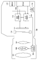
図1は、本発明の第1の実施形態に係わる撮像装置の構成を示すブロック図である。図1において、撮像装置100は、撮像素子111、メカニカルシャッター113、カメラ制御部114、信号処理部115、および操作部117、集光レンズ121、絞り122、フォーカスレンズ123、レンズ制御部124を有する。
<First embodiment>
FIG. 1 is a block diagram showing the configuration of an imaging apparatus according to the first embodiment of the invention. In FIG. 1, the
ユーザーは、操作部117の不図示のAF開始ボタン、撮影開始ボタン、を操作することにより、カメラ制御部114およびレンズ制御部124の制御内容を指定し、AF動作、撮影動作などを行うことができる。また、操作部117にはメニューボタンおよびコントロールボタンも配置されており、メニュー画面を表示部に表示させて、静止画撮影や動画撮影などのカメラの動作内容を設定することができる。
By operating an AF start button and a shooting start button (not shown) of the
また、図2に示すように、撮像素子111と信号処理部115間では、クロックとデータが重畳された信号でデータ伝送を行うエンベデッドクロック方式を用いてデータの送受信が行われる。送信部220は撮像素子111内部のPLLで作られた基準クロックを用いて、データをシリアルデータに変換して、信号処理部115の受信部230に送信する(送信動作)。エンベデッドクロック方式では、受信部230は基準クロックを持たず、送信部220から送られた信号から、クロックを再生し、再生したクロックでデータをパラレルデータに変換して、信号処理部115の後段のブロックに出力する。
Further, as shown in FIG. 2, data transmission/reception is performed between the
受信部230がクロックとデータを再生するために、送信部220は基準となる特定のパターンでHigh、Lowを繰り返すトレーニング用のデータ(トレーニング信号)を送信し、その出力によって受信部230が送信部220の周波数と同期する。
In order for the receiving
信号処理部115は、受信部230に入力された撮像素子111のデータに補正処理と現像処理を施し、画像データを作成する。信号処理部115は、CPUおよび後述する画像処理ブロックや記憶領域としてのRAMなどを構成部品として備える。
The
以下、図2に示すブロック図を参照して、第1の実施形態における撮像素子111と信号処理部115間のデータの流れについて説明する。
The data flow between the
撮像素子111は、画素部201、タイミング制御部211、垂直読出制御部209、水平転送回路205、デジタル処理部207、シリアルI/F213、送信部220を備える。撮像素子111は、撮像装置100の撮影レンズにより撮像素子111上に結像された像信号を、フォトダイオードから成る画素部201で受光し、画素ごとの信号に変換する。列回路203において画素ごとの電圧を順次デジタル変換したデータが、水平転送回路205によりデジタル処理部207に送られ、デジタル処理部207でクランプといったデジタル処理が行われ、送信部220により撮像素子111の外部に出力される。送信部220は、画像データとクロック信号を重畳した重畳信号を送信する。
The
信号処理部115は、複数のレシーバ回路231から成る受信部230を有する。各レシーバ回路231は、CDR回路235、記憶レジスタ237を有し、各レシーバ回路231に入力された信号から、クロックとデータを再生する。
The
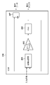
図3は、CDR回路235の構成を示すブロック図である。図3において、CDR回路235は、位相比較器301、ループフィルタ303、VCO(電圧制御発振器)305、データ再生器307を備える。
FIG. 3 is a block diagram showing the configuration of the
位相比較器301は、入力された信号のデータエッジと、VCOの出力クロックの位相を比較し、位相差に応じた電圧値を出力する。ループフィルタ303は、VCO305の応答速度と入力電圧振幅レンジに合わせて位相比較器の出力信号を平滑化し、電圧を増幅する。 VCO305は、入力されるループフィルタ303の電圧振幅に応じた周波数のクロックを出力する。VCO305の出力クロックを位相比較器に帰還させることにより、入力信号との同期を取る。
The
CDR回路235は、初期状態ではどのような周波数と位相のデータが入力されるか不明であり、正しく同期を取ることができないため、起動時に送信部220からトレーニング信号を受け、周波数と位相の同期を取る必要がある(トレーニング期間)。記憶レジスタ237は、CDR回路235のVCO305の出力電圧に応じた設定値を記憶する機能を持つ。また、VCO305の起動時の出力電圧は、記憶レジスタ237の値を参照して決定される。記憶レジスタ237に設定値を書き込むことによりVCO305の起動開始時の出力電圧を決めることができる。
In the initial state, the
位相比較器301は、出力する電圧を調整するためのゲインを掛けることができる。図4は、位相比較器のゲイン量をA倍、B倍(A>B)としたときの、初期の周波数Fsから同期完了後の周波数Ffに至る経時的な変化を簡易的に表した図である。
ゲイン量が大きいほど位相差に応じたフィードバック量が大きく、短時間でFfに近づくことができるが、ゲイン量をA倍とした場合、図4(a)に示すようにオーバーシュートも大きくなる。また、ゲイン量をB倍とした場合、図4(b)に示すように時間はかかるが、オーバーシュートを抑えて同期した後も、その状態が安定する。 The larger the gain amount, the larger the feedback amount corresponding to the phase difference and the closer to Ff in a short time. However, when the gain amount is A times, the overshoot also increases as shown in FIG. 4(a). Further, when the gain amount is B times, as shown in FIG. 4B, although it takes time, the state is stabilized even after synchronizing by suppressing the overshoot.
Ffは、撮像素子111と信号処理部115のデータのスループットをもとに設計でおおよそ決まっているが、FsはVCOの出力周波数の状態で決まるため、撮像装置の起動時に定めることは難しく、起動の度に変動する。撮像装置の起動時は、初期はゲイン量をA倍とし、途中からゲイン量をB倍とすることにより、広い範囲のFsの周波数同期が可能となるようにする。この起動時に行う周波数調整量の大きい周波数同期制御を第1の周波数同期制御と呼ぶ。
Ff is roughly determined by design based on the data throughput of the
トレーニング信号とは、HIGHレベルとLOWレベルが特定のパターンで出力される信号である。トレーニング信号で、同期のとれた状態でVCO305が出力したクロックを、再生クロックと呼ぶこととし、再生クロックを受信信号が入力されたデータ再生器307に供給することにより、受信信号からデータを取り出すことができる。
A training signal is a signal in which a HIGH level and a LOW level are output in a specific pattern. The clock output by the
前述のように、トレーニング信号で同期が取れた後は、送信部220から有効なデータ送信を開始し、データを取り出す。CDR回路235で、クロックとデータが重畳されたシリアルデータ(重畳信号)から再生したデータを再生データと呼ぶこととする。
As described above, after synchronization is achieved with the training signal, the transmitting
また、受信部230が有効なデータを受信している期間は、入力信号のデータエッジと、前述の再生クロックの位相を検出し、CDR回路235内部のVCO305の出力周波数を変化させる。これにより、データ伝送中の温度変化などで周波数や位相がずれても、その変動に追従して、同期状態を保つことができる。
Also, during the period when the receiving
前述のトレーニング信号とは異なり、画像データのようなシリアルデータでは、HIGHやLOWの信号が連続する場合があり、パルスエッジが検出できないため、その状態が長く継続すると、同期が外れてしまうことがある。 Unlike the training signal described above, serial data such as image data may have a series of HIGH and LOW signals, and pulse edges cannot be detected. be.
通常、そういった問題を回避するために送信部220からクロックとデータを重畳したデータを送信する前に、たとえば「8b/10b変換」といった処理を施す。8b/10b変換は、8ビットのデータを10ビットのデータに変換して、HIGHやLOWの信号を4クロック以下とするデータ変換である。有効データの転送効率が低下する代わりに、受信部でパルスエッジを検出することができ、周波数変動に対してロバスト性が向上する。なお、8b/10b変換されたデータは受信部231でデコードする必要がある。これらの処理を撮像素子111の送信部220と信号処理部115の受信部230内の不図示のブロックで行う。
Normally, in order to avoid such a problem, processing such as "8b/10b conversion" is performed before transmitting the data in which the clock and data are superimposed from the
類似の技術として、PCI EXPRESS 3.0/4.0では、「128b/130b変換」があり、これも128ビットの有効データに対して、2ビットのプリアンブル信号を持たせることで、HIGHやLOWの信号が長期間継続しないようにしている。本実施形態においても、「8b/10b変換」に限らず、上述と同様な効果をもつ変換処理を用いてもよい。 As a similar technology, PCI EXPRESS 3.0/4.0 has "128b/130b conversion", which also converts HIGH and LOW by giving 128-bit valid data a 2-bit preamble signal. signal does not continue for a long period of time. Also in this embodiment, conversion processing having the same effect as described above may be used instead of the "8b/10b conversion".
前述のとおり、一度、送受信部で同期を取ることができれば、データ送信が継続する限り、位相同期をすることができる。しかし、撮像装置では、撮像素子の読み出し中以外で送受信部を休止することにより、消費電力を低減する場合がある。このように動画の毎フレームで休止期間を設ける場合、同期は崩れる。しかし、事前のVCOの状態が前回の周波数同期状態に近いため、ゲイン量をB倍として周波数同期制御を開始し、同期状態を復帰する。この撮像素子の休止期間からの復帰時にゲイン量をB倍で行う周波数調整量の小さい周波数同期制御を、第2の周波数同期制御と呼ぶ。この第2の周波数同期制御では、事前のVCOの状態が前回の周波数同期状態に近いため、ゲイン量をB倍としても、第1の周波数同期制御よりも短時間で同期をとることができる。そのため、送信部220からのトレーニング信号の出力期間もそれに応じて短縮することができる。
As described above, once synchronization can be achieved in the transmitting and receiving units, phase synchronization can be achieved as long as data transmission continues. However, in some imaging apparatuses, the power consumption can be reduced by pausing the transmitting/receiving section except during reading of the imaging element. When a pause period is provided in each frame of a moving image in this way, synchronization is lost. However, since the previous state of the VCO is close to the previous frequency synchronization state, the gain amount is multiplied by B and frequency synchronization control is started to restore the synchronization state. The frequency synchronization control with a small amount of frequency adjustment, in which the gain amount is multiplied by B when the imaging device recovers from the idle period, is called the second frequency synchronization control. In this second frequency synchronization control, since the previous state of the VCO is close to the previous frequency synchronization state, even if the gain amount is B times, synchronization can be achieved in a shorter time than in the first frequency synchronization control. Therefore, the output period of the training signal from the
以降では、撮像装置の種々のモードにおいて、送受信部の周波数同期制御を適切に行う制御について説明する。 Hereinafter, control for appropriately performing frequency synchronization control of the transmission/reception unit in various modes of the imaging apparatus will be described.
図5は、撮像装置の静止画撮影における撮像素子と送受信部の駆動を表す模式図である。ユーザーが撮像装置の撮影開始ボタンを操作し静止画撮影を開始する。図5では、撮影開始ボタン操作後、撮影準備(シャッタの通電、チャージや、撮像素子を含む起動シーケンスなど)が完了した状態からの時間の経過を示している。 FIG. 5 is a schematic diagram showing driving of the imaging device and the transmission/reception unit in still image shooting of the imaging device. A user operates a shooting start button of the imaging device to start shooting a still image. FIG. 5 shows the passage of time from the completion of shooting preparations (energization of the shutter, charging, activation sequence including the imaging device, etc.) after the shooting start button is operated.
カメラ制御部114は、撮像素子111に対して、制御信号を供給して指示するとともに、シリアルI/F213を介してレジスタ設定を行う。これにより、撮像素子111の状態を適宜変更し、撮影に必要な蓄積、読み出しを制御するとともに、送信部220の動作制御を行う。撮像素子111は、外部からのデジタル値をシリアルI/F213で受け付け、不図示のレジスタに記憶させることにより、レジスタの内容を動作に反映することができる。
The
撮像装置100では、撮像素子111とカメラ制御部114の間で垂直同期信号VDにより、撮像制御のタイミングの同期がとられている。垂直同期信号VDは、撮像素子111とカメラ制御部114で、次の動作の開始や1フレームの画素の読み出し開始の同期をとるための同期信号である。
In the
また、レジスタ237は、デジタル値が書き込まれた直後に反映される「即時反映レジスタ」と、撮像素子111の状態遷移の同期信号である垂直同期信号VDの立下りエッジに同期して反映される「VD同期レジスタ」を有する。状態遷移の際に変更する必要のある値が「VD同期レジスタ」に格納されるように割り当てておくことにより、状態遷移の変更内容を、設定の順序などによらず同期信号VDに同期して、一括してレジスタに反映させることができる。また、本実施形態では、送受信部の制御には、撮像装置の起動や停止の状態を即座に反映させるため、「即時反映レジスタ」を用いる。
In addition, the
次に、本実施形態の撮像装置の起動時における周波数同期制御について、静止画撮影の場合を例に挙げて説明する。 Next, the frequency synchronization control at the startup of the imaging apparatus according to the present embodiment will be described by taking still image shooting as an example.
静止画撮影を行うために、撮像素子は「蓄積」、「読み出し」、「停止」の動作を行う。「蓄積」の動作は、撮像素子111の画素部201の全画素のフォトダイオードで一括して電荷を排出し、その後に電荷蓄積を行う動作である。「読み出し」の動作は、この動作に移行する以前にフォトダイオードに蓄積されていた電荷を1行ごとに列回路203に転送し、AD変換を行った後に、水平転送回路205からデジタル処理部207に送る動作である。デジタル処理部207では、クランプ処理やゲイン処理を行う。「停止」の動作は、通信期間以外において撮像素子111のクロック供給を停止させて動作を停止させる動作である。静止画撮影では、撮像素子の「蓄積」、「読み出し」、「停止」の動作を順に実行させることにより、「蓄積」動作で蓄積させた電荷から画像データを得る。
In order to capture a still image, the imaging device performs "accumulation", "readout", and "stop" operations. The “accumulation” operation is an operation of collectively discharging charges from the photodiodes of all pixels of the
図5に示した垂直同期信号VDは、撮像素子111に対して状態遷移を行わせるための制御信号である。本実施形態では、垂直同期信号VDのパルスの立下りが検知され、その時点でVD同期レジスタに設定されている設定が回路に反映されて、状態遷移が行われる。撮影準備が完了した状態では送受信部はともに停止状態(停止中)であり、消費電力が小さい。
A vertical synchronizing signal VD shown in FIG. 5 is a control signal for causing the
図5に示す通り、撮像素子111を起動させた際に、前述した第1の周波数同期制御を行い、撮像素子111の起動ごとに変動する送受信部の周波数の同期を取る。そして、第1の周波数同期制御の完了後に、一旦撮像素子111の送信部220と、信号処理部115の受信部230を休止させる。
As shown in FIG. 5, when the
起動後に撮影のシーケンスを行うために、最初の垂直同期信号VD1の前に、「蓄積」状態に移行するレジスタ設定を撮像素子にしておく。これにより、垂直同期信号VD1に同期して所定期間のすべての画素に対する一括リセット動作が行われ、リセットの解除とともに蓄積が開始される。その後、カメラ制御部114は、シャッタ131に対して、蓄積時間に応じたシャッタの開閉制御を行う。
In order to perform the photographing sequence after activation, the image pickup device is set in a register to shift to the "accumulation" state before the first vertical synchronization signal VD1. As a result, a collective reset operation is performed for all pixels in a predetermined period in synchronization with the vertical synchronization signal VD1, and accumulation is started when the reset is released. After that, the
シャッタが閉じた後の2番目の垂直同期信号VD2により、撮像素子111を「読み出し」状態にして、画素の信号を順次送信部220から出力させる。このとき、各レーンの記憶レジスタ237には、前回の第1の周波数同期制御を行った時の電圧値が記憶されており、各受信部230は前回の周波数同期時に近い状態で動作を再開する。カメラ制御部114は、読み出しを開始させる垂直同期信号VD2よりも前(所定時間前)に、第2の周波数同期制御を行う。
By the second vertical synchronization signal VD2 after the shutter is closed, the
このように、受信部230が前回の周波数同期時に近い状態で動作を再開できる場合、第1の周波数同期制御よりも第2の周波数同期制御を行った方が同期できるまでの時間を短くできる。そのため、読み出し前において第2の周波数同期を行うことにより、周波数同期にかかる時間を短縮することができ、その分だけ送受信部の停止期間を長くし、消費電力を軽減することができる。
In this way, when the receiving
垂直同期信号VD2により、撮像素子を「読み出し」状態にし、順次画素毎のデジタルデータを読み出すとともに、送信部220からデータを送信させる。画素数分のデータ受信完了とともに受信部230の動作を停止させ、その後で送信部220の動作を停止させる。3番目の垂直同期信号VD3は、上記の一連のデータ送受信に関わる制御が完了した後に撮像素子111を「停止」状態にするためのトリガとなる。
The vertical synchronizing signal VD2 puts the imaging element into a “readout” state, sequentially reads out digital data for each pixel, and causes the
次に、送受信部220の休止状態からの復帰の際の周波数同期制御について、動画撮影またはライブビュー駆動を例に挙げて説明する。
Next, the frequency synchronization control when the transmitting/receiving
撮像素子11から読み出した画像データをリアルタイムに表示部118に表示するライブビュー駆動を行うために、撮像素子111は「スリットローリング(SR)」動作と、「停止」動作を行う。「SR」動作では、「SR読み出し」動作と「SRリセット」動作の両方、もしくはそのどちらかを行う。
In order to perform live view driving for displaying image data read out from the image pickup device 11 on the
「SR読み出し」動作では、垂直同期信号VDに同期して、行ごとに順次画素の読み出しを行う。「SRリセット」動作では、垂直同期信号VDを基準としたカウント信号(カウント値)が予め設定された値となったときに、行毎に画素の電荷を排出し、その後、電荷蓄積を行う。「SR」動作では、「SRリセット」動作から「SR読み出し」動作までの間隔で撮像素子111の露光時間を制御する。また、「SRリセット」動作だけ、もしくは「SR読み出し」動作だけを行う場合は、シリアルI/F213から、タイミング制御部211のレジスタ設定を行うことにより適宜切り替えることが可能である。
In the "SR readout" operation, pixels are sequentially read out row by row in synchronization with the vertical synchronization signal VD. In the "SR reset" operation, when the count signal (count value) based on the vertical synchronization signal VD reaches a preset value, the charges of the pixels are discharged for each row, and then charges are accumulated. In the "SR" operation, the exposure time of the
図6は、動画撮影における撮像素子と送受信部の駆動を表す模式図である。動画撮影の場合、一定間隔で撮影するためにVDはフレーム同期信号として用いられる。 FIG. 6 is a schematic diagram showing the driving of the imaging element and the transmission/reception unit in moving image shooting. In the case of moving image shooting, VD is used as a frame synchronization signal for shooting at regular intervals.
動画撮影の際の撮像素子の起動は、ユーザーの操作で撮像装置の電源が入れられたときに行われ、前述の静止画と同じように第1の周波数同期制御により、送受信部の準備を行う。動画撮影またはライブビュー駆動では、撮像素子を「SR」動作させて、1フレーム内で画素からの信号読み出し動作(SR読み出し動作)と、次フレームのためのリセット動作(SRリセット動作)を制御する。また本実施形態では、読み出し画素数やフレームレートの異なる複数の動画撮影モードをもち、それぞれのモードで信号読み出しに必要な時間は異なる。 Activation of the imaging device during video shooting is performed when the power of the imaging device is turned on by the user's operation, and the transmission/reception unit is prepared by the first frequency synchronization control in the same way as the still image described above. . In video shooting or live view driving, the image sensor is operated in "SR" mode to control the signal readout operation (SR readout operation) from the pixels within one frame and the reset operation (SR reset operation) for the next frame. . In addition, the present embodiment has a plurality of moving image shooting modes with different numbers of readout pixels and frame rates, and the time required for signal readout differs in each mode.
図6では、そのうちの一つのモードでの一連の制御について詳細に説明する。図6の最初の垂直同期信号VD1に同期して、撮像素子111の画素部201は1回目のSR読み出し動作「SR読み出し1」を行い、そのときの画素毎のデジタルデータを送受信部220が受信部230に送信する。フレームごとの画素数分のデータ受信完了とともに非読み出し期間に受信部230の動作を停止させ、その後で送信部220の動作を停止させる。
A series of controls in one of these modes will be described in detail in FIG. In synchronization with the first vertical synchronization signal VD1 in FIG. 6, the
本実施形態では、垂直読出制御部209と送受信部220でクロック系統が分離されているため、送受信部220が停止期間中でも、次のフレームのためのSRリセット動作である「SRリセット2」を実行することができる。
In this embodiment, since the clock system is separated between the vertical
次のフレームの先頭からデータ送受信を行うために、次の垂直同期信号VD2よりも前に撮像素子111の送信部220にトレーニング信号出力を行わせるように即時反映レジスタに設定する。即時反映レジスタの反映と同時に、送信部220は、トレーニング信号の出力を開始する。その後、カメラ制御部114は、受信部230の起動および第2の周波数同期制御を開始する。このとき、記憶レジスタ237には、第1の周波数同期制御を行った時の電圧値が記憶されており、各受信部230は前回の周波数同期時に近い状態で動作を再開する。
In order to perform data transmission/reception from the beginning of the next frame, the immediate reflection register is set so that the
送信部220のトレーニング信号の出力開始は受信部230の第2の周波数同期制御の開始以前とする。受信部230が前回の周波数同期時に近い状態で動作を再開できる場合、第1の周波数同期制御よりも第2の周波数同期制御を行った方が同期できるまでの時間を短くできる。そのため、第2の周波数同期制御を行うことにより、フレームレートが高く、撮像素子111のデータ送信の間隔が短い場合にも送受信部を停止させ、消費電力を軽減させることができる。
It is assumed that the output of the training signal from the
上記の説明では、本実施形態の効果を示すための撮像装置の撮影モードの一例を示しており、たとえば、画像データが大きく撮像素子のデータ送信の間隔が極端に短い撮影モードでは送受信部の停止・復帰を行わないなど、モード毎に制御を切り替えてもよい。 In the above description, an example of the shooting mode of the imaging device for demonstrating the effects of the present embodiment is shown.・The control may be switched for each mode, such as not returning.
また、撮像装置は、撮像素子から間引き読み出しをするライブビュー駆動から、全画素読み出しをして静止画相当の画像を取得する制御を行う。ライブビューと静止画では要求されるデータスルーレートが異なるため、撮像素子111と信号処理部115をつなぐ伝送レーンの数をモードの変更とともに変更する。
In addition, the image capturing apparatus performs control to obtain an image equivalent to a still image by performing all-pixel readout from live view driving in which thinning readout is performed from the image sensor. Since the required data slew rate differs between live view and still image, the number of transmission lanes connecting the
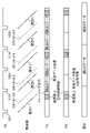
図7は、撮像素子の画素の読み出し方式が途中で変更され、伝送レーン数が変更された場合の送受信部の動作状態を示す模式図である。静止画とライブビューの両方で共通に使用する伝送レーンの送信部、受信部をそれぞれTX(Gr1)、RX(Gr1)とし、静止画のみで使用する伝送レーンの送信部、受信部をそれぞれTX(Gr2)、RX(Gr2)として示している。 FIG. 7 is a schematic diagram showing the operating state of the transmitting/receiving unit when the pixel reading method of the imaging element is changed in the middle and the number of transmission lanes is changed. TX (Gr1) and RX (Gr1) are the transmission and reception sections of the transmission lanes used for both still images and live view, respectively, and the transmission and reception sections of the transmission lanes used only for still images are respectively TX. (Gr2) and RX (Gr2).
図7のように、撮影モードに応じて、伝送レーン数を変える制御により送受信部の消費電力を抑える。また、静止画のみで使用する伝送レーンの送受信部は、ライブビュー中は停止状態であり、停止状態が継続するほど、前回の周波数同期状態からの変化が大きくなるため、第1の周波数同期制御を行う。以下、詳細に説明する。 As shown in FIG. 7, the power consumption of the transmission/reception unit is suppressed by controlling the number of transmission lanes to be changed according to the imaging mode. In addition, the transmission/reception unit of the transmission lane used only for still images is in a stopped state during live view, and the longer the stopped state, the greater the change from the previous frequency synchronization state. I do. A detailed description will be given below.
2番目の垂直同期信号VD2以前ではライブビュー駆動のための「SR読み出し」動作を行っている。図6と同じように、ライブビューの「SR読み出し」状態では、Gr1の送受信部に対して、フレーム毎に第2の周波数同期制御を実施する。 Before the second vertical synchronizing signal VD2, the "SR reading" operation for driving the live view is performed. As in FIG. 6, in the live view "SR readout" state, the second frequency synchronization control is performed for each frame for the Gr1 transmitting/receiving unit.
垂直同期信号VD2~VD3の期間は全画素のリセット走査のみを行う「SRリセット」動作を行う。この区間では、「一括リセット蓄積」動作と同じく、画素部の読み出しを行わないため、これ以前の撮像素子の状態によらず、送受信部を停止する。 During the period of the vertical synchronizing signals VD2 to VD3, the "SR reset" operation of only reset scanning of all pixels is performed. In this period, as in the "batch reset accumulation" operation, since the readout of the pixel portion is not performed, the transmitting/receiving portion is stopped regardless of the state of the image sensor before this period.
次の垂直同期信号VD3から「SR読み出し」動作を行い画像データを読み出す。そのために、カメラ制御部114が受信部230の位相同期完了に必要な時間を算出し、タイマーによってその時間だけ読み出し開始のVD3よりも前にトレーニング信号の出力が開始されるように即時反映レジスタに設定する。
From the next vertical synchronization signal VD3, the "SR reading" operation is performed to read out the image data. For this purpose, the
次フレームの先頭からデータ送受信を行うために、次のVD3よりも前に伝送レーンごとに下記のように制御する。 In order to perform data transmission/reception from the beginning of the next frame, the following control is performed for each transmission lane prior to the next VD3.
ライブビュー時に使用していなかった伝送レーンの同期を取るために、カメラ制御部114は、撮像素子111の送信部220であるTX(Gr2)からトレーニング信号出力を行うように即時反映レジスタに設定する。即時反映レジスタの反映と同時に送信部220であるTX(Gr2)は、トレーニング信号の出力を開始する。その後、カメラ制御部114は、受信部230であるRX(Gr2)の起動および第1の周波数同期制御を開始させる。
In order to synchronize the transmission lanes that were not used during live view, the
一方、ライブビュー時に使用していた伝送レーンの同期を取るために、カメラ制御部114は、撮像素子111の送信部220であるTX(Gr1)からトレーニング信号出力を行うように即時反映レジスタに設定する。即時反映レジスタの反映と同時に送信部220であるTX(Gr1)は、トレーニング信号の出力を開始する。その後、カメラ制御部114は、受信部230であるRX(Gr1)の起動および第2の周波数同期制御を開始させる。
On the other hand, in order to synchronize the transmission lanes used during live view, the
送信部220であるTX(Gr1)、TX(Gr2)のトレーニング信号の出力開始は、それぞれの対応する受信部230であるRX(Gr1)、RX(Gr2)の周波数同期制御の開始以前とする。また、送信部220であるTX(Gr2)とRX(GR2)の周波数同期制御のタイミングは、カメラ制御部114および信号処理部115の処理負荷の混雑時を避け、次の垂直同期信号VDに間に合うように制御すればよく、できるだけ長く送受信部を停止させる。
TX (Gr1) and TX (Gr2), which are transmitting
なお、上記のように伝送レーンごとにトレーニング信号の出力を開始しないことも可能である。送信部220であるTX(Gr2)のトレーニング信号の出力開始とともに送信部220であるTX(Gr1)についてもトレーニング信号の出力を開始するようにしてもよい。
It is also possible not to start outputting the training signal for each transmission lane as described above. TX (Gr1), which is the
垂直同期信号VD3~VD4の期間は、撮像素子111が「SR読み出し」動作を行い、順次画素毎のデジタルデータを読み出すとともに、送信部220からデータを送信する。受信部230がデータ受信を完了したら、送受信部を停止する。
During the period of the vertical synchronizing signals VD3 to VD4, the
垂直同期信号VD4~VD5の期間は、画素を間引き読み出しする場合の「SRリセット」動作を行う。画素部201の読み出しを行わないため、これ以前の撮像素子111の状態によらず、送受信部を停止することができ、消費電力を軽減することができる。
During the period of the vertical synchronizing signals VD4 to VD5, the "SR reset" operation for thinning out pixels is performed. Since the
次の垂直同期信号VD5では「SR読み出し」動作を行い、画像データを読み出すために、VD5よりも前からトレーニング信号を出力開始させるように、即時反映レジスタに設定する。垂直同期信号VD5以降は、垂直同期信号VD2以前の「SR読み出し」動作と同じようにGr1の送受信部に対して、フレーム毎に第2の周波数同期制御を実施する。 At the next vertical synchronizing signal VD5, the "SR reading" operation is performed, and in order to read out the image data, the immediate reflection register is set so as to start outputting the training signal before VD5. After the vertical synchronizing signal VD5, the second frequency synchronizing control is performed for each frame for the transmitting/receiving unit of Gr1 in the same manner as the "SR read" operation before the vertical synchronizing signal VD2.
このような一連の制御により、モードに応じて伝送レーン数を増減する場合、特に伝送レーン数を少なくした場合に、撮像素子111と信号処理部115の送受信部の消費電力を軽減することが可能となる。
With such a series of controls, when the number of transmission lanes is increased or decreased according to the mode, especially when the number of transmission lanes is reduced, the power consumption of the transmission/reception units of the
以上説明したように、本実施形態によれば、撮像装置のモードに応じて、撮像素子111と信号処理部115のデータ伝送の消費電力を効果的に軽減することが可能となる。
As described above, according to the present embodiment, it is possible to effectively reduce the power consumption for data transmission between the
<第2の実施形態>
この第2の実施形態では、撮像装置100、撮像素子111、信号処理部115、CDR回路235の構成は、図1、図2、及び図3に示す第1の実施形態と同様であるため、その説明は省略する。第2の実施形態では、各伝送レーンのCDR回路235の記憶レジスタ237の設定値から、VCO(電圧制御発振器)305の電圧を定めることができる。起動前に記憶レジスタ237に設定することにより、設定値に対応したVCO電圧から動作を開始する。
<Second embodiment>
In the second embodiment, the configurations of the
また、第1の周波数同期制御、第2の周波数同期制御、または有効データの送受信で随時、その時点での周波数同期情報に記憶レジスタが更新され、記憶レジスタの設定を読むことで、そのときのVCO電圧を知ることができる。 In addition, the memory register is updated with the frequency synchronization information at that point in time by the first frequency synchronization control, the second frequency synchronization control, or transmission/reception of valid data, and by reading the setting of the memory register, the current information can be obtained. VCO voltage can be known.
カメラ制御部114は、実際に撮像装置100が使用される前に、全伝送レーンに第1の周波数同期制御を行い、その同期状態におけるVCO電圧を、周波数同期情報として、レーンごとに図1に不図示のフラッシュメモリに書き込んでおく。周波数同期情報は全伝送レーンを同時に同期状態にした際のVCO出力電圧を再現するための情報である。次回以降の起動時に、周波数同期情報をCDR回路235の記憶レジスタ237に書き込むことにより、VCO電圧を周波数同期情報を取得したときの電圧に設定する。
Before the
周波数同期情報の取得は製造時に行い、フラッシュメモリに書き込んでおくものとする。ただし、撮像装置100の初回起動時もしくは電源が入るたびに行ってもよい。
It is assumed that the frequency synchronization information is acquired at the time of manufacture and written in the flash memory. However, it may be performed when the
図8に示すように、モードにより伝送レーンを変更する場合においては、以下のような制御を行う。 As shown in FIG. 8, when changing the transmission lane depending on the mode, the following control is performed.
図8は図7と同様に、間引き読み出しをするライブビュー駆動から、全画素読み出しをして静止画相当の画像を取得する制御に移行する動作を模式的に示している。 Similar to FIG. 7, FIG. 8 schematically shows the operation of shifting from live view driving with thinning readout to control of acquiring an image equivalent to a still image with all-pixel readout.
図8では、モードによらず継続的に使用する伝送レーンでは、随時各レーンのCDR回路235の周波数同期情報が更新されている。そのため、記憶レジスタ237を読み出してフラッシュメモリに記憶した情報と比較することにより、環境温度などによる周波数のずれを予測できる。予測された周波数のずれ分を考慮して、長期間使用していない伝送レーンの復帰時に記憶レジスタに書き込むことにより、その伝送レーンにおいても第2の周波数同期制御で送受信部の同期を取ることができる。
In FIG. 8, in the transmission lanes that are continuously used regardless of the mode, the frequency synchronization information of the
以降は、図7と図8の制御の違いについてのみ説明する。垂直同期信号VD2以前では、ライブビュー駆動のための「SR読み出し」動作を行っており、垂直同期信号VD2~VD3までの期間が図7と異なる制御となる。 Hereinafter, only differences between the controls in FIGS. 7 and 8 will be described. Before the vertical synchronizing signal VD2, the "SR readout" operation for driving the live view is performed, and the period from the vertical synchronizing signals VD2 to VD3 is controlled differently from that in FIG.
垂直同期信号VD2~VD3の期間で、図8のSRリセット2で示すように画素部を行ごとにリセットし、静止画撮影のための全画素のリセット走査を行う。SRリセット2の走査を垂直同期信号VD2の直後に開始させ、垂直同期信号VD2~VD3の期間のフレーム周期2期間を増減することにより、静止画の蓄積時間を決定する。
During the period of the vertical synchronizing signals VD2 to VD3, the pixel portion is reset row by row as indicated by SR reset 2 in FIG. 8, and reset scanning of all pixels for still image shooting is performed. The SR reset 2 scan is started immediately after the vertical synchronizing signal VD2, and the
また、垂直同期信号VD2~VD3の期間では、受信部230であるRX(Gr1)に含まれる伝送レーンの一つを基準レーンとし、基準レーンの記憶レジスタ情報を読み出す。次にフラッシュメモリから各伝送レーンの周波数同期情報を読み出す。基準レーンの記憶レジスタ情報から基準レーンの周波数同期情報を減算し、周波数同期補正値を算出する。各伝送レーンの周波数同期情報に周波数同期補正値を加算して、各伝送レーンの記憶レジスタに対して設定する。
Also, during the period of the vertical synchronization signals VD2 to VD3, one of the transmission lanes included in RX (Gr1), which is the receiving
カメラ制御部114は、送信部220であるTX(Gr1)、TX(Gr2)にトレーニング信号を出力するように即時反映レジスタに設定する。即時反映レジスタの反映と同時に送信部220であるTX(Gr1)、TX(Gr2)は、トレーニング信号の出力を開始する。
The
その後、カメラ制御部114は、受信部230であるRX(Gr1)、RX(Gr2)の起動および第2の周波数同期制御を開始させる。送信部220であるTX(Gr1)、TX(Gr2)のトレーニング信号の出力開始は、受信部230であるRX(Gr1)、RX(Gr2)の周波数同期制御の開始以前とする。送受信部TX(Gr1)とRX(GR1)、TX(Gr2)とRX(GR2)は、一律、第2の周波数同期制御により対応するデバイスと同期を取ることができる。
After that, the
以上説明したように、本実施形態の制御により、伝送レーン数を増加させた場合に短時間で送受信部の同期状態を復帰することが可能となり、静止画の蓄積時間を決めるフレーム周期を短く設定することができる。 As described above, with the control of this embodiment, when the number of transmission lanes is increased, the synchronous state of the transmitting and receiving units can be restored in a short period of time, and the frame period that determines the accumulation time of still images is set short. can do.
なお、本実施形態は一例であり、静止画の蓄積時間を本実施形態と異なる形態で制御する場合にも適用可能である。 Note that this embodiment is an example, and can be applied to a case where the storage time of still images is controlled in a form different from that of this embodiment.
<第3の実施形態>
この第3の実施形態では、 撮像装置100、撮像素子111、信号処理部115、CDR回路235の構成は、図1、図2、及び図3に示す第1の実施形態と同様であるため、その説明は省略する。第1の実施形態では、図5、図6で説明したように、受信部の周波数同期制御の前に撮像素子111の送信部220がトレーニング信号を出力する必要がある。撮像装置100では、撮像素子111とカメラ制御部114が垂直同期信号VDおよび水平同期信号HDにより、撮像制御のタイミング同期を取っている。
<Third Embodiment>
In the third embodiment, the configurations of the
垂直同期信号VDは、撮像素子111とカメラ制御部114で、次の動作の開始や1フレームの画素の読み出し開始の同期をとるための同期信号である。また、水平同期信号HDは、1ラインの画素の読み出し開始の同期をとるための同期信号である。
The vertical synchronizing signal VD is a synchronizing signal for synchronizing the start of the next operation and the start of reading out pixels of one frame between the
また、カメラ制御部114は、水平同期信号の立下りエッジをカウントするHDカウンタを有し、あらかじめ設定した回数の立下りを検知した際に割込信号を発行することが可能である。カメラ制御部114は、HDカウンタが発行した割込信号をトリガにして、あらかじめ決められた制御を開始することができる。
The
図9は動画撮影時に水平同期信号の立下りエッジのカウントで発行した割込信号で周波数同期制御を行うことを示す模式図である。 FIG. 9 is a schematic diagram showing that frequency synchronization control is performed by an interrupt signal issued by counting the falling edge of the horizontal synchronization signal during moving image shooting.
図9は、図6と同じように毎フレームで、撮像素子を「SR」動作させて、1フレーム内で画素からの信号読み出し動作(SR読み出し動作)と、次フレームのためのリセット動作(SRリセット動作)を制御する。フレームごとに画素数分のデータの受信完了とともに受信部230の動作を停止させ、その後で送信部220の動作を停止させる。
In FIG. 9, the image pickup device is operated in the “SR” mode in each frame as in FIG. reset operation). The operation of the receiving
次フレームの読み出しのために、送信部220からトレーニング信号を出力する第1のタイミングと、受信部230が第2の周波数同期制御を開始する第2のタイミングをカメラ制御部114のHDカウンタに設定する。
In order to read out the next frame, the HD counter of the
HDカウンタのHDの立下りエッジ検出数が第1のタイミングと一致すると、HDカウンタは割込信号1を発行する。割込信号1により、カメラ制御部114は撮像素子111に対して、トレーニング信号出力開始を設定し、トレーニング信号の出力が開始される。HDカウンタのHDの立下りエッジ検出数が第2のタイミングと一致すると、HDカウンタは割込信号2を発行する。割込信号2により、カメラ制御部114は受信部230に第2の周波数同期制御の開始を設定し、第2の周波数同期制御が実行される。
When the number of HD falling edges detected by the HD counter matches the first timing, the HD counter issues an interrupt
HDカウンタの割込信号を用いることにより、撮像素子111の動作状態と同期した周波数同期制御を行うことができる。そのため、タイマ処理などで非同期に制御するよりも、撮像素子の読み出し間隔が短いモードでも、送受信部の停止、復帰制御を行うことが可能となる。
By using the interrupt signal of the HD counter, frequency synchronization control synchronized with the operating state of the
本実施形態では、動画撮影を例に説明したが、静止画撮影の際には、蓄積時間に応じて、第1のタイミング、第2のタイミングをHDカウンタに設定することにより、有効データの読み出しの前に送受信部の周波数同期制御を行うことができる。 In the present embodiment, moving image shooting has been described as an example, but in the case of still image shooting, valid data can be read out by setting the first timing and second timing in the HD counter according to the accumulation time. frequency synchronization control of the transmitting/receiving unit can be performed before
また、水平同期信号HDの立下りエッジの検出によりタイミングの制御を行う例を示したが、次の状態遷移が開始されるタイミングを計ることができるものであれば、別の目的の同期信号でもよく、検出する極性も種々の形態をとることが可能である。 Also, an example of controlling the timing by detecting the falling edge of the horizontal synchronizing signal HD has been shown, but a synchronizing signal for another purpose can be used as long as the timing at which the next state transition is started can be measured. Well, the detected polarity can also take various forms.
本実施形態の制御により、撮像素子の読み出し間隔が短いモードにおいても、撮像素子111と信号処理部115のデータ伝送の消費電力を軽減することが可能となる。
The control of this embodiment makes it possible to reduce power consumption for data transmission between the
<第4の実施形態>
この第4の実施形態では、撮像装置100、撮像素子111、信号処理部115の構成は、図1及び図2に示す第1の実施形態と同様であるため、その説明は省略する。
<Fourth Embodiment>
In the fourth embodiment, the configurations of the
図10は、第4の実施形態におけるCDR回路235の構成を示すブロック図である。図10において、CDR回路235は、位相比較器301、ループフィルタ303、VCO(電圧制御発振器)305、フリップフロップ309を備える。
FIG. 10 is a block diagram showing the configuration of the
位相比較器301は、入力された信号のデータエッジと、VCO305の出力クロックの位相を比較し、位相差に応じた電圧値を出力する。ループフィルタ303は、VCO305の応答速度と入力電圧振幅レンジに合わせて位相比較器301の出力信号を平滑化し、電圧を増幅する。 VCO305は、入力されるループフィルタ303の電圧振幅に応じた周波数のクロックを出力する。VCO305の出力クロックを位相比較器301に帰還させることにより、入力信号との同期を取る。
The
CDR回路235は、初期状態ではどのような周波数と位相のデータが入力されるか不明であり、正しく同期を取ることができないため、起動時に送信部220からトレーニング信号を受け、周波数と位相の同期を取る必要がある。
In the initial state, the
トレーニング信号とは、HIGHレベルとLOWレベルが特定のパターンで出力される信号である。トレーニング信号で、同期のとれた状態でVCO305が出力したクロックを、再生クロックと呼ぶこととし、再生クロックを受信信号が入力されたフリップフロップ309に供給することにより、受信信号からデータを取り出すことができる。
A training signal is a signal in which a HIGH level and a LOW level are output in a specific pattern. A clock output from the
前述のように、トレーニング信号で同期が取れた後は、送信部220から有効なデータ送信を開始し、データを取り出す。CDR回路235で、クロックとデータが重畳されたシリアルデータから再生したデータを再生データと呼ぶこととする。
As described above, after synchronization is achieved with the training signal, the transmitting
また、受信部230が有効なデータを受信している期間は、入力信号のデータエッジと、前述の再生クロックの位相を検出し、同期制御をすることにより、データ伝送中の温度変化などで周波数や位相がずれても、その変動に追従して、同期状態を保つことができる。
In addition, during the period when the receiving
前述のトレーニング信号とは異なり、画像データのような一般的なシリアルデータでは、HIGHやLOWの信号が連続する場合があり、パルスエッジが検出できないため、その状態が長く継続すると、同期が外れてしまうことがある。 Unlike the training signal described above, general serial data such as image data may have a series of HIGH and LOW signals, and pulse edges cannot be detected. I can put it away.
通常、そういった問題を回避するために送信部220からクロックとデータを重畳したデータを送信する前に、たとえば「8b/10b変換」といった処理を施す。8b/10b変換は、8ビットのデータを10ビットのデータに変換して、HIGHやLOWの信号を4クロック以下とするデータ変換である。有効データの転送効率が低下する代わりに、受信部でパルスエッジを検出することができ、周波数変動に対してロバスト性が向上する。なお、8b/10b変換されたデータは受信部231でデコードする必要がある。これらの処理を撮像素子111の送信部220と信号処理部115の受信部230内の不図示のブロックで行う。
Normally, in order to avoid such a problem, processing such as "8b/10b conversion" is performed before transmitting the data in which the clock and data are superimposed from the
類似の技術として、PCI EXPRESS 3.0/4.0では、「128b/130b変換」があり、これも128ビットの有効データに対して、2ビットのプリアンブル信号を持たせることで、HIGHやLOWの信号が長期間継続しないようにしている。本実施形態においても、「8b/10b変換」に限らず、上述と同様な効果をもつ変換処理を用いてもよい。 As a similar technology, PCI EXPRESS 3.0/4.0 has "128b/130b conversion", which also converts HIGH and LOW by giving 128-bit valid data a 2-bit preamble signal. signal does not continue for a long period of time. Also in this embodiment, conversion processing having the same effect as described above may be used instead of the "8b/10b conversion".
前述のとおり、一度、送受信部で同期を取ることができれば、データ送信が継続する限り、位相同期をとることができる。しかし、撮像装置では、撮像素子の読み出し中以外で送受信部を休止することにより、消費電力を低減する場合がある。 As described above, once synchronization can be achieved in the transmitting and receiving units, phase synchronization can be achieved as long as data transmission continues. However, in some imaging apparatuses, the power consumption can be reduced by pausing the transmitting/receiving section except during reading of the imaging element.
以降では、撮像装置の種々のモードにおいて、送受信部での消費電力を低減するための制御について説明する。 Hereinafter, control for reducing power consumption in the transmission/reception unit in various modes of the imaging apparatus will be described.
図11は、撮像装置100の静止画撮影中の撮像素子111と送受信部の駆動を表す模式図である。ユーザーが撮像装置100の撮影開始ボタンを操作し静止画撮影を開始する。図11では、撮影開始ボタンの操作後、撮影準備(シャッタの通電&チャージや、撮像素子を含む起動シーケンスなど)が完了した状態からの時間の経過を示している。
FIG. 11 is a schematic diagram showing driving of the
カメラ制御部114は、撮像素子111に対して、制御信号を供給するとともに、シリアルI/F213を介してレジスタ設定を行うことにより、撮像素子111の状態を適宜変更し、撮影に必要な蓄積、読み出しを制御するとともに、送信部220の動作を制御する。撮像素子111は、外部からのデジタル値をシリアルI/F213で受け付け、不図示のレジスタに記憶させることにより、レジスタの内容を動作に反映することができる。また、レジスタにはデジタル値が書き込まれた直後に反映される「即時反映レジスタ」と、撮像素子111の状態遷移の同期信号である垂直同期信号VDの立下りエッジに同期して反映する「VD同期レジスタ」が含まれる。状態遷移の際に変更する必要のあるものを「VD同期レジスタ」に割り当てておくことにより、状態遷移の変更内容を設定の順序などによらず、垂直同期信号VDに同期して、一括して反映させることができる。また、本実施形態では、送受信部の制御に関わるレジスタには、撮像装置の起動や停止のときに即座に反映させるため、「即時反映レジスタ」を用いる。
The
静止画撮影を行うために、撮像素子は「蓄積」、「読み出し」、「停止」の動作を行う。「蓄積」の動作は、撮像素子111の画素部201の全画素のフォトダイオードで一括して電荷を排出し、その後に電荷蓄積を行う動作である。「読み出し」の動作は、この動作に移行する以前にフォトダイオードに蓄積されていた電荷を1行ごとに列回路203に転送し、AD変換を行った後に、水平転送回路205からデジタル処理部207に送る動作である。デジタル処理部207では、クランプ処理やゲイン処理を行う。「停止」の動作は、撮像素子111のクロック供給を停止させて動作を停止させる動作である。静止画撮影では、撮像素子の「蓄積」、「読み出し」、「停止」の動作を順に実行させることにより、「蓄積」動作で蓄積させた電荷から画像データを得る。
In order to capture a still image, the imaging device performs "accumulation", "readout", and "stop" operations. The “accumulation” operation is an operation of collectively discharging charges from the photodiodes of all pixels of the
図11に示した垂直同期信号VDは、撮像素子111に対して状態遷移を行わせるための制御信号であり、本実施形態では垂直同期信号VDパルスの立下りを検知し、その時点でVD同期レジスタに設定されている設定を回路に反映し状態遷移を行わせる。撮影準備が完了した状態では送受信部はともに停止状態とし、電力を消費しない。
The vertical synchronizing signal VD shown in FIG. 11 is a control signal for causing the
図11の最初の垂直同期信号VD1の前に、「蓄積」動作を行わせる設定を撮像素子111のレジスタに設定しておくことにより、垂直同期信号VD1に同期して全ての画素に対して一括してリセットが行われ、リセットの解除とともに蓄積が開始される。その後、カメラ制御部114は、シャッタ113に対して、蓄積時間に応じた開閉制御を行う。
Prior to the first vertical synchronizing signal VD1 in FIG. 11, setting to perform the "accumulation" operation is set in the register of the
シャッタが閉じた後の2番目の垂直同期信号VD2により、撮像素子111に「読み出し」動作を行わせ、画素から読み出したデジタル信号を順次送信部220から出力させる。カメラ制御部114は、読み出しを開始させる垂直同期信号VD2よりも前に、撮像素子111のレジスタに対して送信部220からトレーニング信号を出力させる設定を行い、同時に信号処理部115の受信部230に位相同期を開始させる。
The second vertical synchronization signal VD2 after the shutter is closed causes the
また、受信部230の位相同期は、VCO305の出力するクロックの安定待ちなどのために完了するまでに有限の時間が必要である。その間、トレーニング信号の出力も受信部230の同期の完了が保証されるまで確保する必要ある。そのため、カメラ制御部114が受信部の位相同期完了のために必要な時間を換算し、タイマにより、その時間だけ読み出し開始のVD2よりも前に、トレーニング信号の出力開始を即時反映レジスタに設定する。即時反映レジスタの反映と同時に、送信部220は、トレーニング信号の出力を開始する。その後、カメラ制御部114は、受信部230の起動および位相同期を開始させる。
Further, the phase synchronization of the receiving
垂直同期信号VD2で、撮像素子111に「読み出し」動作を行わせ、順次画素毎のデジタルデータを読み出すとともに、送信部220からデータを送信する。画素数分のデータの受信完了とともに受信部230の動作を停止させ、その後に送信部220の動作を停止させる。3番目の垂直同期信号VD3は、上記の一連のデータ送受信に関わる制御が完了した後に撮像素子111を「停止」動作させるためのトリガとなる。
The vertical synchronizing signal VD2 causes the
本実施形態では、動画撮影動作、もしくは撮影画像をリアルタイムに表示部118に表示するライブビュー動作を行うために、撮像素子111は「スリットローリング(SR)」動作、「停止」動作を行う。
In this embodiment, the
「SR」動作では、「SR読み出し」動作と「SRリセット」動作の両方、もしくはそのどちらかを行う。「SR読み出し」動作では、垂直同期信号VDに同期して、行ごとに順次画素の読み出しを行う。「SRリセット」動作では、垂直同期信号VDを基準としたカウント信号が、予め設定された値となったときに行毎に画素の電荷を排出し、その後、電荷蓄積を行う。 In the 'SR' operation, either or both of the 'SR read' operation and the 'SR reset' operation are performed. In the "SR readout" operation, pixels are sequentially read out row by row in synchronization with the vertical synchronization signal VD. In the "SR reset" operation, when the count signal based on the vertical synchronizing signal VD reaches a preset value, the charges of the pixels are discharged row by row, and then the charges are accumulated.
「SR」動作では、「SRリセット」動作から「SR読み出し」動作までの間隔で撮像素子の露光時間が制御される。また、「SRリセット」動作だけ、もしくは「SR読み出し」動作だけを行う場合は、シリアルI/F213から、タイミング制御部211のレジスタを設定することにより適宜変更することが可能である。
In the "SR" operation, the exposure time of the image sensor is controlled at intervals from the "SR reset" operation to the "SR readout" operation. Also, when only the “SR reset” operation or only the “SR read” operation is performed, it is possible to change the setting appropriately by setting the register of the
図12は、動画撮影中の撮像素子111と送受信部の駆動を表す模式図である。動画撮影の場合、一定間隔で撮影するために垂直同期信号VDはフレーム同期信号としても用いられる。動画撮影動作またはライブビュー動作では、撮像素子111に「SR」動作を行わせ、1フレーム内で画素からの信号読み出し動作(SR読み出し動作)と、次フレームのためのリセット動作(SRリセット動作)を制御する。また、本実施形態では、読み出し画素数やフレームレートの異なる複数の動画撮影モードを持ち、それぞれのモードで信号読み出しに必要な時間は異なる。
FIG. 12 is a schematic diagram showing the driving of the
図12では、そのうちの一つのモードに関する一連の制御について詳細に説明する。図12に記載の最初の垂直同期信号VD1に同期して、撮像素子111の画素部201は1回目のSR読み出し動作「SR読み出し1」を行い、そのときの画素毎のデジタルデータを送信部220から受信部230に送信する。フレームごとの画素数分のデータの受信完了とともに受信部230の動作を停止させ、その後に送信部220の動作を停止させる。
FIG. 12 details a series of controls for one of these modes. In synchronization with the first vertical synchronization signal VD1 shown in FIG. to the receiving
本実施形態では、垂直読出制御部209と送受信部230でクロック系統が分離されているため、送受信部が停止期間中でも、次のフレームのためのSRリセット動作である「SRリセット2」で画素部201を走査することができる。カメラ制御部が受信部230の位相同期完了に必要な時間を換算し、タイマによって、その時間だけ次の垂直同期信号VD2よりも前にトレーニング信号の出力開始を即時反映レジスタに設定する。即時反映レジスタの反映と同時に送信部220は、トレーニング信号の出力を開始する。
In this embodiment, since the clock system is separated between the vertical
その後、カメラ制御部114は、受信部230の起動および位相同期を開始させる。この一連の制御を繰り返し行うことにより、動画撮影の際にデータ転送に不要な期間の送受信部にかかる電力を抑えることができる。
After that, the
ただし、フレームレートが早く、フレーム周期に対して読み出しにかかる時間が長い場合、読み出し完了から次のVDまでの期間内に位相同期完了に必要な時間が確保できないことがある。 However, when the frame rate is high and the readout takes a long time with respect to the frame period, the time required for completion of phase synchronization may not be ensured within the period from the completion of readout to the next VD.
図13は、動画撮影中にフレームレートが変更された場合の送受信部の動作状態を示す模式図であり、この図を用いて、フレームレートに応じた送受信部の停止制御について説明する。 FIG. 13 is a schematic diagram showing the operating state of the transmitting/receiving unit when the frame rate is changed during moving image shooting. Using this diagram, stop control of the transmitting/receiving unit according to the frame rate will be described.
図13における「フレーム周期1」は、位相同期完了に必要な時間が確保できるフレーム周期を示し、「フレーム周期2」は、位相同期完了に必要な時間が確保できないフレーム周期を示している。
"
「フレーム周期1」の図12と同様な動画撮影状態から、「フレーム周期2」の撮影状態に変更された場合、読み出し完了後に送受信回路の停止を行わず、送信部220は画素数分のデータ送信が完了した後にダミーデータを送信する。ダミーデータは任意のデータで良く、たとえばトレーニング信号でもよい。送受信部の停止制御を行うかどうかは、フレーム周期から読み出しに必要な時間を除いたブランキング期間の長さで判断する。読み出しに必要な時間は動画撮影モードによって異なり、動画撮影モードとフレームレートによりブランキング期間が決まる。
When the moving image shooting state of “
具体的には、カメラ制御部114が、動作中のモードとフレームレートとからブランキング時間を算出し、ブランキング時間が予め決められた所定の長さ以上の場合にのみ、前述の停止制御と復帰の際の同期制御を行い、それ以外の場合は停止制御も同期制御も行わない。
Specifically, the
また、撮像装置100は、撮像素子111から間引き読み出しをするライブビュー駆動から、全画素読み出しをして静止画相当の画像を取得する制御を行うことがある。
In addition, the
図14は、撮像素子111の画素の読み出し方式が途中で変更された場合の送受信部の動作状態を示す模式図である。図14における各区間で撮像素子111の動作を切替えて、撮像素子111の動作に応じて送受信部の制御を変更することにより、このような撮像素子の状態遷移での消費電力を抑えるように送受信部の制御を行う。
FIG. 14 is a schematic diagram showing the operating state of the transmission/reception unit when the pixel reading method of the
2番目の垂直同期信号VD2以前では、ライブビュー駆動のための「SR読み出し」動作を行っている。図12、図13と同じように、「SR読み出し」状態では、フレーム周期に対するモードごとの閾値を設定し、カメラ制御部114がフレーム周期が閾値以上であるかどうかを判定し、閾値以上の場合に送受信部の停止制御および位相同期制御を実施する。
Before the second vertical synchronizing signal VD2, the "SR reading" operation for driving the live view is performed. As in FIGS. 12 and 13, in the “SR reading” state, a threshold is set for each mode with respect to the frame period, and the
垂直同期信号VD2~VD3の期間は全画素のリセット走査のみを行う「SRリセット」動作を行う。この区間では、「一括リセット蓄積」動作と同じく、画素部の読み出しを行わないため、これ以前の撮像素子の状態によらず、送受信部を停止する。 During the period of the vertical synchronizing signals VD2 to VD3, the "SR reset" operation of only reset scanning of all pixels is performed. In this period, as in the "batch reset accumulation" operation, since the readout of the pixel portion is not performed, the transmitting/receiving portion is stopped regardless of the state of the image sensor before this period.
次の垂直同期信号VD3から「SR読み出し」動作を行い、画像データを読み出すために、カメラ制御部114が受信部230の位相同期完了に必要な時間を算出し、タイマによって、その時間だけ読み出し開始の垂直同期信号VD3よりも前に、トレーニング信号の出力開始を即時反映レジスタに設定する。垂直同期信号VD3~VD4の期間は、撮像素子111が「SR読み出し」動作を行い、順次画素毎のデジタルデータを送信部220から受信部230へ送信する。
In order to perform the "SR reading" operation from the next vertical synchronization signal VD3 and read out the image data, the
垂直同期信号VD4~VD5の期間は、画素を間引き読み出しする場合のリセット走査である「SRリセット」動作を実行する。画素部の読み出しを行わないため、これ以前の撮像素子の状態によらず、送受信部を停止する。 During the period of the vertical synchronizing signals VD4 to VD5, the "SR reset" operation, which is reset scanning when thinning out the pixels, is performed. Since the pixel portion is not read out, the transmitting/receiving portion is stopped regardless of the state of the image sensor before this.
次の垂直同期信号VD5では、「SR読み出し」動作を行い、画像データを読み出すために、垂直同期信号VD5よりも前からトレーニング信号の出力開始を即時反映レジスタに設定する。垂直同期信号VD5以降は、「SR読み出し」動作を行わせ、フレーム周期1と閾値を参照して、送受信部を復帰させる時間を決め、送受信部を停止し、次の垂直同期信号VDよりも前にトレーニング信号出力を開始させる制御を繰り返す。
With the next vertical synchronizing signal VD5, the "SR reading" operation is performed, and in order to read out the image data, the output start of the training signal is set in the immediate reflection register before the vertical synchronizing signal VD5. After the vertical synchronizing signal VD5, the "SR reading" operation is performed, the
上記の一連の制御により、撮像素子111の画素の読み出し方式が途中で変更された場合にも、データ転送が必要なとき以外は、送受信部を停止させ、消費電力を低減することができる。
Through the series of controls described above, even when the pixel reading method of the
<第5の実施形態>
第4の実施形態での送受信部の位相同期制御に関しては、十分に位相同期が完了する固有の位相同期時間を想定しているため、停止状態から位相同期を取る場合には常に同じだけの時間がかかる。しかし、読み出し時間に対するフレーム周期が短くなるにつれて、送受信部の停止期間が短くなることにより、消費電力が大きくなる高フレームレートの動画での電力低減効果が得られなくなる。
<Fifth Embodiment>
Regarding the phase synchronization control of the transmitting and receiving units in the fourth embodiment, since it is assumed that the phase synchronization time is unique enough to complete the phase synchronization, the same amount of time is always required to obtain phase synchronization from the stopped state. It takes However, as the frame cycle with respect to the readout time becomes shorter, the stop period of the transmitting/receiving unit becomes shorter, so that the power reduction effect cannot be obtained for high frame rate moving images that consume a large amount of power.
第5の実施形のCDR回路は、図3のループフィルタ303に電圧保持回路を備え、カメラ制御部114からの制御信号により電圧保持と電圧保持の解除を制御する。トレーニング信号による同期制御の完了後、送信部220の停止前にその時点での電圧を保持し、復帰時にその電圧をVCO305に入力する。これにより、受信信号と位相差の小さい状態から同期制御が開始でき、位相同期に必要な時間を短縮することができる。位相同期制御を行う際には、送信部220からの信号が入力された後に、ループフィルタ303の電圧保持の解除を行う。この制御では、受信部230は完全に停止することができないが、送信部220の動作停止を行うことができる。
The CDR circuit of the fifth embodiment includes a voltage hold circuit in the
図15は、上記の待機状態から位相同期を行う場合の制御を示す模式図である。図15における最初の垂直同期信号VD1は、送信部220と受信部230がともに停止状態であるときに最初に入力された垂直同期信号である。
FIG. 15 is a schematic diagram showing control when phase synchronization is performed from the standby state described above. The first vertical synchronizing signal VD1 in FIG. 15 is the vertical synchronizing signal that is first input when both the
受信部230が停止状態にある場合は、垂直同期信号VD1から開始される撮像素子111のSR読み出し1のデータの受信の前に、第4の実施形と同じように所定の期間のトレーニング出力を受信して、位相同期制御を行う。このときの位相同期制御に必要な期間を位相同期制御期間1とする。
When the receiving
その後、SR読み出し1のデータの受信が完了したときにカメラ制御部114の制御信号によりループフィルタ303の電圧を保持する。その後に送信部220を停止させ、受信部230を電圧保持状態で待機させる。受信部230を待機状態から復帰させる際に必要な期間を、位相同期制御期間2としたとき、位相同期制御期間2は、位相同期制御期間1よりも短くなる。
After that, the voltage of the
2番目の垂直同期信号VD2で開始される撮像素子111の読み出し動作よりも位相同期制御期間2だけ早く、送信部220からトレーニング信号の出力を開始する。そして、ループフィルタ303の電圧保持状態を解除し、受信部230の位相同期を行い、SR読み出し2のデータを受信する。SR読み出し2のデータ受信完了後に、カメラ制御部114の制御信号によりループフィルタ303の電圧を保持し、その後に送信部220を停止させ、受信部230を電圧保持状態で待機させる。
The
3番目の垂直同期信号VD3以降は、垂直同期信号VD2の場合と同様に、データ受信完了後に受信部230を待機状態にさせ、データ受信前に待機状態からの位相同期制御を繰り返す。
After the third vertical synchronizing signal VD3, similarly to the case of the vertical synchronizing signal VD2, the receiving
このように制御することにより、高フレームレートの動画においても、消費電力を低減することが可能となる。 By controlling in this way, it is possible to reduce power consumption even in high-frame-rate moving images.
<第6の実施形態>
以下、図16のブロック図を参照して、本発明の第6の実施形態における、撮像素子111と信号処理部115の間のデータの流れについて説明する。第6の実施形態では、撮像素子111の内部に画像データを一時的に記憶するメモリ223を持つことにより、第4の実施形の構成ではできない駆動モードに対しても、送受信部での消費電力の低減を行うことができる。
<Sixth embodiment>
Data flow between the
撮像素子111の読み出しの高速化により、120fpsの高フレームレートで画素信号を読み出して動画記録し、動画の表示を60fpsで行うスローモーション動画の撮影が行えるようになってきている。スローモーション動画の撮影をする場合も、撮影時はリアルタイムの表示が求められるために、高フレームレートで読み出した一部のフレームのみを表示に用いる。表示のフレームレート(表示周期)は、撮像装置100の表示部118に依存し、現在普及している60fps程度を用いる。
Due to the increased readout speed of the
図17は、表示用フレームと記録用フレームの撮影を周期的に繰り返す場合の送受信部の動作状態を示す模式図である。図17における垂直同期信号VD1~VD2の期間は、記録のみに用いるフレームを取得し、垂直同期信号VD2~VD3の期間は表示と記録の両方に用いるフレームを取得し、これ以降は、この繰り返しである。 FIG. 17 is a schematic diagram showing the operating state of the transmitting/receiving unit when the display frame and the recording frame are periodically photographed. During the period of the vertical synchronization signals VD1 to VD2 in FIG. 17, frames used only for recording are obtained, and during the periods of the vertical synchronization signals VD2 to VD3, frames used for both display and recording are obtained. be.
垂直同期信号VD1~VD2の期間で読み出されたデータはメモリ223に溜めておき、この期間のデータは送信をしない(記録用フレーム)。垂直同期信号VD2~VD3の期間のデータは、読み出しと同時に送信され、信号処理部115で表示に使えるよう画像処理を施され、表示部118に表示される(表示用フレーム)。
The data read during the period of the vertical synchronization signals VD1 and VD2 are stored in the
撮像素子111は、表示用フレームのデータ送信完了後に、メモリ223に溜めていた記録用フレームのデータを送信し、受信部230は、表示用フレームと記録用フレームのデータの受信が完了してから、停止する。
After the data transmission of the display frame is completed, the
信号処理部115は、表示用フレームを取得するとともに撮像装置111の表示部118に表示するための画像生成処理を行う。さらに、信号処理部115は、順次受信した記録用フレームを不図示のDRAMに記憶させておき、表示用フレーム間の記録用フレームの画像取得完了後に、表示用フレームと記録用フレームを露光時刻順に並べ替えて動画像を生成する。生成された動画像は、記録メディアに記憶される。
The
上記のように制御することにより、位相同期制御の回数を減らし、その分を停止期間にあてることで、消費電力を低減することができる。さらに、メモリ223に一度溜めたデータは、撮像素子111から直接読み出すよりも、AD変換などにかかる時間の制約を受けずに済むため、より高い周波数でデータ伝送を行うことができる。
By controlling as described above, power consumption can be reduced by reducing the number of times of phase synchronization control and allocating it to the stop period. Furthermore, data once stored in the
以上、本発明の好ましい実施形態について説明したが、本発明はこれらの実施形態に限定されず、その要旨の範囲内で種々の変形及び変更が可能である。 Although preferred embodiments of the present invention have been described above, the present invention is not limited to these embodiments, and various modifications and changes are possible within the scope of the gist.
(その他の実施形態)
また本発明は、上述の実施形態の1以上の機能を実現するプログラムを、ネットワーク又は記憶媒体を介してシステム又は装置に供給し、そのシステム又は装置のコンピュータにおける1つ以上のプロセッサーがプログラムを読出し実行する処理でも実現できる。また、1以上の機能を実現する回路(例えば、ASIC)によっても実現できる。
(Other embodiments)
In addition, the present invention supplies a program that implements one or more functions of the above-described embodiments to a system or apparatus via a network or a storage medium, and one or more processors in the computer of the system or apparatus reads the program. It can also be realized by executing processing. It can also be implemented by a circuit (eg, ASIC) that implements one or more functions.
10:撮像装置、111:撮像素子、115:信号処理部、114:カメラ制御部、201:画素部、220:送信部、230:受信部、235:CDR回路 10: imaging device, 111: imaging element, 115: signal processing unit, 114: camera control unit, 201: pixel unit, 220: transmission unit, 230: reception unit, 235: CDR circuit
Claims (19)
前記重畳信号を前記撮像素子の送信手段から受信する受信手段を有し、前記画像データとクロックとを再生する画像処理手段と、
前記撮像素子と前記画像処理手段とを制御する制御手段と、を備え、
前記制御手段は、前記送信手段が前記画像データの送信を開始する前に、前記送信手段から、前記送信手段と前記受信手段の周波数同期をとるためのトレーニング信号を送信させるように制御し、
前記受信手段は、周波数同期された状態の設定値を記憶するレジスタを有し、前記送信手段と同期をとるための第1の周波数同期制御と第2の周波数同期制御とを切り替えることが可能であり、
前記第1の周波数同期制御及び前記第2の周波数同期制御は、前記受信手段が前記画像データを再生するために用いるクロックを前記トレーニング信号と比較した結果をフィードバックすることによって、前記送信手段と前記受信手段の周波数同期をとるものであって、
前記第1の周波数同期制御は、前記第2の周波数同期制御よりも、前記フィードバックを行うためのゲイン量が大きく、
前記制御手段は、前記第1の周波数同期制御または前記第2の周波数同期制御を行った後に、周波数同期制御を行う場合には、前記レジスタに記憶された設定値に基づいて、前記第2の周波数同期制御を行うことを特徴とする撮像装置。 an imaging device having a pixel section in which a plurality of pixels are arranged; and a transmission means for transmitting a superimposed signal obtained by superimposing image data obtained from the pixel section and a clock;
image processing means for reproducing the image data and the clock, having receiving means for receiving the superimposed signal from the transmitting means of the imaging device;
and a control means for controlling the imaging element and the image processing means,
The control means causes the transmission means to transmit a training signal for synchronizing the frequencies of the transmission means and the reception means before the transmission means starts transmitting the image data,
The receiving means has a register for storing a set value in a frequency-synchronized state, and is capable of switching between first frequency synchronization control and second frequency synchronization control for synchronizing with the transmitting means. can be,
The first frequency synchronization control and the second frequency synchronization control are performed by feeding back a result of comparing a clock used by the receiving means to reproduce the image data with the training signal, thereby controlling the transmitting means and the for frequency synchronization of receiving means,
The first frequency synchronization control has a larger gain amount for performing the feedback than the second frequency synchronization control, and
When performing frequency synchronization control after performing the first frequency synchronization control or the second frequency synchronization control, the control means performs the second frequency synchronization control based on the setting value stored in the register. An imaging device characterized by performing frequency synchronization control .
前記制御手段は、前記記録用フレームの画像データを前記記憶手段に記憶させておき、前記表示用フレームの画像データの読み出しに同期したタイミングで送信させ、前記記憶手段に記憶していた記録用フレームを前記表示用フレームのデータ送信完了後に送信させることを特徴とする請求項1に記載の撮像装置。 The imaging element further includes storage means for temporarily storing the image data, and the imaging device includes display means for displaying a part of the frames of the image data as display frames at a predetermined display cycle; further comprising image processing means for generating a moving image in which the remaining frames of the image data are used as recording frames, and the display frames and the recording frames are arranged chronologically;
The control means causes the image data of the recording frame to be stored in the storage means, transmits the image data of the display frame in synchronization with the reading of the image data of the display frame, and transmits the image data of the recording frame stored in the storage means. is transmitted after data transmission of the display frame is completed.
前記撮像素子と前記画像処理手段とを制御する制御工程を備え、
前記制御工程では、前記送信手段が前記画像データの送信を開始する前に、前記送信手段から、前記送信手段と前記受信手段の周波数同期をとるためのトレーニング信号を送信させるように制御し、
前記受信手段は、周波数同期された状態の設定値を記憶するレジスタを有し、前記送信手段と同期をとるための第1の周波数同期制御と第2の周波数同期制御とを切り替えることが可能であり、
前記第1の周波数同期制御及び前記第2の周波数同期制御は、前記受信手段が前記画像データを再生するために用いるクロックを前記トレーニング信号と比較した結果をフィードバックすることによって、前記送信手段と前記受信手段の周波数同期をとるものであって、
前記第1の周波数同期制御は、前記第2の周波数同期制御よりも、前記フィードバックを行うためのゲイン量が大きく、
前記制御工程では、前記第1の周波数同期制御または前記第2の周波数同期制御を行った後に、周波数同期制御を行う場合には、前記レジスタに記憶された設定値に基づいて、前記第2の周波数同期制御を行うことを特徴とする撮像装置の制御方法。 An imaging device having a pixel section in which a plurality of pixels are arranged, a transmitting means for transmitting a superimposed signal obtained by superimposing image data obtained from the pixel section and a clock, and a transmitting means of the imaging device for transmitting the superimposed signal. A method for controlling an imaging device comprising: receiving means for receiving from, and image processing means for reproducing the image data and a clock,
A control step of controlling the imaging element and the image processing means,
In the control step, before the transmitting means starts transmitting the image data, the transmitting means is controlled to transmit a training signal for synchronizing the frequencies of the transmitting means and the receiving means;
The receiving means has a register for storing a setting value in a frequency-synchronized state, and is capable of switching between first frequency synchronization control and second frequency synchronization control for synchronizing with the transmitting means. can be,
The first frequency synchronization control and the second frequency synchronization control are performed by feeding back a result of comparing a clock used by the receiving means to reproduce the image data with the training signal, thereby controlling the transmitting means and the for frequency synchronization of receiving means,
The first frequency synchronization control has a larger gain amount for performing the feedback than the second frequency synchronization control,
In the control step, when frequency synchronization control is performed after performing the first frequency synchronization control or the second frequency synchronization control, the second frequency synchronization control is performed based on the set value stored in the register. A control method for an imaging device, characterized by performing frequency synchronization control .
Priority Applications (2)
| Application Number | Priority Date | Filing Date | Title |
|---|---|---|---|
| JP2018184985A JP7175697B2 (en) | 2018-09-28 | 2018-09-28 | IMAGING DEVICE AND CONTROL METHOD THEREOF, PROGRAM, STORAGE MEDIUM |
| US16/576,897 US10979626B2 (en) | 2018-09-28 | 2019-09-20 | Image capturing apparatus, method of controlling same, and storage medium for reducing power consumption in transmission of image data |
Applications Claiming Priority (1)
| Application Number | Priority Date | Filing Date | Title |
|---|---|---|---|
| JP2018184985A JP7175697B2 (en) | 2018-09-28 | 2018-09-28 | IMAGING DEVICE AND CONTROL METHOD THEREOF, PROGRAM, STORAGE MEDIUM |
Publications (3)
| Publication Number | Publication Date |
|---|---|
| JP2020057844A JP2020057844A (en) | 2020-04-09 |
| JP2020057844A5 JP2020057844A5 (en) | 2021-11-04 |
| JP7175697B2 true JP7175697B2 (en) | 2022-11-21 |
Family
ID=69945279
Family Applications (1)
| Application Number | Title | Priority Date | Filing Date |
|---|---|---|---|
| JP2018184985A Active JP7175697B2 (en) | 2018-09-28 | 2018-09-28 | IMAGING DEVICE AND CONTROL METHOD THEREOF, PROGRAM, STORAGE MEDIUM |
Country Status (2)
| Country | Link |
|---|---|
| US (1) | US10979626B2 (en) |
| JP (1) | JP7175697B2 (en) |
Families Citing this family (3)
| Publication number | Priority date | Publication date | Assignee | Title |
|---|---|---|---|---|
| CN111526314B (en) * | 2020-04-24 | 2022-04-05 | 荣耀终端有限公司 | Video shooting method and electronic device |
| JP7744139B2 (en) * | 2021-02-15 | 2025-09-25 | 浜松ホトニクス株式会社 | Intraoral imaging device |
| CN116367001B (en) * | 2023-03-20 | 2025-05-27 | 中国科学院长春光学精密机械与物理研究所 | Image sensor serial data dynamic training method |
Citations (5)
| Publication number | Priority date | Publication date | Assignee | Title |
|---|---|---|---|---|
| JP2004236051A (en) | 2003-01-31 | 2004-08-19 | Renesas Technology Corp | Synchronizing circuit and method |
| JP2009225197A (en) | 2008-03-17 | 2009-10-01 | Sony Corp | Imaging apparatus, signal processing method, and computer program |
| JP2011170644A (en) | 2010-02-19 | 2011-09-01 | Sony Corp | Communication device, communication system, and communication method |
| JP2015080702A (en) | 2013-10-24 | 2015-04-27 | Hoya株式会社 | Endoscope device |
| JP2016208208A (en) | 2015-04-21 | 2016-12-08 | キヤノン株式会社 | Imaging device |
Family Cites Families (9)
| Publication number | Priority date | Publication date | Assignee | Title |
|---|---|---|---|---|
| JPH03278794A (en) * | 1990-03-28 | 1991-12-10 | Nec Corp | Channel circuit |
| JPH06334892A (en) * | 1993-05-20 | 1994-12-02 | Fujitsu General Ltd | CCTV camera |
| JP2970843B2 (en) * | 1997-04-17 | 1999-11-02 | 日本電気株式会社 | PLL circuit |
| US7443426B2 (en) * | 2004-02-13 | 2008-10-28 | Canon Kabushiki Kaisha | Image capturing system and control method of the same |
| JP2009201540A (en) | 2008-02-26 | 2009-09-10 | Fujinon Corp | Imaging system and endoscope system |
| JP5888914B2 (en) | 2011-09-22 | 2016-03-22 | キヤノン株式会社 | Imaging apparatus and control method thereof |
| JP5793253B2 (en) * | 2013-04-30 | 2015-10-14 | 株式会社フジクラ | Transmission device, reception device, transmission / reception system, transmission method, and reception method |
| JP6711612B2 (en) | 2015-12-21 | 2020-06-17 | キヤノン株式会社 | Image processing apparatus, image processing method, and imaging apparatus |
| JP6085739B1 (en) * | 2016-04-12 | 2017-03-01 | 株式会社セレブレクス | Low power consumption display device |
-
2018
- 2018-09-28 JP JP2018184985A patent/JP7175697B2/en active Active
-
2019
- 2019-09-20 US US16/576,897 patent/US10979626B2/en active Active
Patent Citations (5)
| Publication number | Priority date | Publication date | Assignee | Title |
|---|---|---|---|---|
| JP2004236051A (en) | 2003-01-31 | 2004-08-19 | Renesas Technology Corp | Synchronizing circuit and method |
| JP2009225197A (en) | 2008-03-17 | 2009-10-01 | Sony Corp | Imaging apparatus, signal processing method, and computer program |
| JP2011170644A (en) | 2010-02-19 | 2011-09-01 | Sony Corp | Communication device, communication system, and communication method |
| JP2015080702A (en) | 2013-10-24 | 2015-04-27 | Hoya株式会社 | Endoscope device |
| JP2016208208A (en) | 2015-04-21 | 2016-12-08 | キヤノン株式会社 | Imaging device |
Also Published As
| Publication number | Publication date |
|---|---|
| US20200106957A1 (en) | 2020-04-02 |
| JP2020057844A (en) | 2020-04-09 |
| US10979626B2 (en) | 2021-04-13 |
Similar Documents
| Publication | Publication Date | Title |
|---|---|---|
| JP5817664B2 (en) | Imaging apparatus, imaging method, and program | |
| TWI513321B (en) | An image processing apparatus, an information processing apparatus, an information processing system, and a frame data output synchronization method | |
| CN106134173B (en) | Display control unit and display equipment | |
| JP7175697B2 (en) | IMAGING DEVICE AND CONTROL METHOD THEREOF, PROGRAM, STORAGE MEDIUM | |
| CN101729782B (en) | Imaging apparatus and imaging method | |
| EP3065128B1 (en) | Imaging device | |
| JP6645279B2 (en) | Imaging equipment | |
| US20070013807A1 (en) | Digital camera | |
| US11356603B2 (en) | Image capturing apparatus and control method therefor | |
| US8279309B2 (en) | Image capturing device with signal sampling | |
| JP7224831B2 (en) | Imaging device | |
| US20130058618A1 (en) | Imaging device and imaging method | |
| CN113014795A (en) | Control apparatus, control method, image pickup apparatus, image pickup system, and storage medium | |
| JP2012029223A (en) | Image sensor and imaging apparatus | |
| JP6728010B2 (en) | Imaging device and method for controlling imaging device | |
| JP2008118239A (en) | IMAGING DEVICE AND IMAGING DEVICE CONTROL METHOD | |
| JP2013098877A (en) | Stereo imaging device, synchronous imaging method and electronic information apparatus | |
| JP6042676B2 (en) | Imaging device | |
| JP7696607B2 (en) | Imaging device | |
| JP2012124678A (en) | Imaging apparatus and imaging apparatus control program | |
| JP2021040269A (en) | Imaging device and its control method and program | |
| JP4974497B2 (en) | Imaging device | |
| JP2016058963A (en) | Imaging device and control method for the same | |
| JP4753658B2 (en) | Imaging device | |
| JP4785445B2 (en) | Imaging device |
Legal Events
| Date | Code | Title | Description |
|---|---|---|---|
| RD01 | Notification of change of attorney |
Free format text: JAPANESE INTERMEDIATE CODE: A7421 Effective date: 20210103 |
|
| A521 | Request for written amendment filed |
Free format text: JAPANESE INTERMEDIATE CODE: A523 Effective date: 20210113 |
|
| A521 | Request for written amendment filed |
Free format text: JAPANESE INTERMEDIATE CODE: A523 Effective date: 20210924 |
|
| A621 | Written request for application examination |
Free format text: JAPANESE INTERMEDIATE CODE: A621 Effective date: 20210924 |
|
| A977 | Report on retrieval |
Free format text: JAPANESE INTERMEDIATE CODE: A971007 Effective date: 20220707 |
|
| A131 | Notification of reasons for refusal |
Free format text: JAPANESE INTERMEDIATE CODE: A131 Effective date: 20220722 |
|
| A521 | Request for written amendment filed |
Free format text: JAPANESE INTERMEDIATE CODE: A523 Effective date: 20220914 |
|
| TRDD | Decision of grant or rejection written | ||
| A01 | Written decision to grant a patent or to grant a registration (utility model) |
Free format text: JAPANESE INTERMEDIATE CODE: A01 Effective date: 20221011 |
|
| A61 | First payment of annual fees (during grant procedure) |
Free format text: JAPANESE INTERMEDIATE CODE: A61 Effective date: 20221109 |
|
| R151 | Written notification of patent or utility model registration |
Ref document number: 7175697 Country of ref document: JP Free format text: JAPANESE INTERMEDIATE CODE: R151 |