JP7174060B2 - Measurement of multi-layer stacks - Google Patents
Measurement of multi-layer stacks Download PDFInfo
- Publication number
- JP7174060B2 JP7174060B2 JP2020545097A JP2020545097A JP7174060B2 JP 7174060 B2 JP7174060 B2 JP 7174060B2 JP 2020545097 A JP2020545097 A JP 2020545097A JP 2020545097 A JP2020545097 A JP 2020545097A JP 7174060 B2 JP7174060 B2 JP 7174060B2
- Authority
- JP
- Japan
- Prior art keywords
- test sample
- interference
- data
- compensated
- interface
- Prior art date
- Legal status (The legal status is an assumption and is not a legal conclusion. Google has not performed a legal analysis and makes no representation as to the accuracy of the status listed.)
- Active
Links
Images


Classifications
-
- G—PHYSICS
- G01—MEASURING; TESTING
- G01B—MEASURING LENGTH, THICKNESS OR SIMILAR LINEAR DIMENSIONS; MEASURING ANGLES; MEASURING AREAS; MEASURING IRREGULARITIES OF SURFACES OR CONTOURS
- G01B9/00—Measuring instruments characterised by the use of optical techniques
- G01B9/02—Interferometers
- G01B9/0209—Low-coherence interferometers
-
- G—PHYSICS
- G01—MEASURING; TESTING
- G01B—MEASURING LENGTH, THICKNESS OR SIMILAR LINEAR DIMENSIONS; MEASURING ANGLES; MEASURING AREAS; MEASURING IRREGULARITIES OF SURFACES OR CONTOURS
- G01B9/00—Measuring instruments characterised by the use of optical techniques
- G01B9/02—Interferometers
- G01B9/02001—Interferometers characterised by controlling or generating intrinsic radiation properties
- G01B9/02002—Interferometers characterised by controlling or generating intrinsic radiation properties using two or more frequencies
-
- G—PHYSICS
- G01—MEASURING; TESTING
- G01B—MEASURING LENGTH, THICKNESS OR SIMILAR LINEAR DIMENSIONS; MEASURING ANGLES; MEASURING AREAS; MEASURING IRREGULARITIES OF SURFACES OR CONTOURS
- G01B11/00—Measuring arrangements characterised by the use of optical techniques
- G01B11/02—Measuring arrangements characterised by the use of optical techniques for measuring length, width or thickness
- G01B11/026—Measuring arrangements characterised by the use of optical techniques for measuring length, width or thickness by measuring distance between sensor and object
-
- G—PHYSICS
- G01—MEASURING; TESTING
- G01B—MEASURING LENGTH, THICKNESS OR SIMILAR LINEAR DIMENSIONS; MEASURING ANGLES; MEASURING AREAS; MEASURING IRREGULARITIES OF SURFACES OR CONTOURS
- G01B11/00—Measuring arrangements characterised by the use of optical techniques
- G01B11/02—Measuring arrangements characterised by the use of optical techniques for measuring length, width or thickness
- G01B11/06—Measuring arrangements characterised by the use of optical techniques for measuring length, width or thickness for measuring thickness ; e.g. of sheet material
- G01B11/0616—Measuring arrangements characterised by the use of optical techniques for measuring length, width or thickness for measuring thickness ; e.g. of sheet material of coating
- G01B11/0675—Measuring arrangements characterised by the use of optical techniques for measuring length, width or thickness for measuring thickness ; e.g. of sheet material of coating using interferometry
-
- G—PHYSICS
- G01—MEASURING; TESTING
- G01B—MEASURING LENGTH, THICKNESS OR SIMILAR LINEAR DIMENSIONS; MEASURING ANGLES; MEASURING AREAS; MEASURING IRREGULARITIES OF SURFACES OR CONTOURS
- G01B11/00—Measuring arrangements characterised by the use of optical techniques
- G01B11/14—Measuring arrangements characterised by the use of optical techniques for measuring distance or clearance between spaced objects or spaced apertures
-
- G—PHYSICS
- G01—MEASURING; TESTING
- G01B—MEASURING LENGTH, THICKNESS OR SIMILAR LINEAR DIMENSIONS; MEASURING ANGLES; MEASURING AREAS; MEASURING IRREGULARITIES OF SURFACES OR CONTOURS
- G01B11/00—Measuring arrangements characterised by the use of optical techniques
- G01B11/24—Measuring arrangements characterised by the use of optical techniques for measuring contours or curvatures
- G01B11/2441—Measuring arrangements characterised by the use of optical techniques for measuring contours or curvatures using interferometry
-
- G—PHYSICS
- G01—MEASURING; TESTING
- G01B—MEASURING LENGTH, THICKNESS OR SIMILAR LINEAR DIMENSIONS; MEASURING ANGLES; MEASURING AREAS; MEASURING IRREGULARITIES OF SURFACES OR CONTOURS
- G01B9/00—Measuring instruments characterised by the use of optical techniques
- G01B9/02—Interferometers
- G01B9/02001—Interferometers characterised by controlling or generating intrinsic radiation properties
- G01B9/02002—Interferometers characterised by controlling or generating intrinsic radiation properties using two or more frequencies
- G01B9/02004—Interferometers characterised by controlling or generating intrinsic radiation properties using two or more frequencies using frequency scans
-
- G—PHYSICS
- G01—MEASURING; TESTING
- G01B—MEASURING LENGTH, THICKNESS OR SIMILAR LINEAR DIMENSIONS; MEASURING ANGLES; MEASURING AREAS; MEASURING IRREGULARITIES OF SURFACES OR CONTOURS
- G01B9/00—Measuring instruments characterised by the use of optical techniques
- G01B9/02—Interferometers
- G01B9/02001—Interferometers characterised by controlling or generating intrinsic radiation properties
- G01B9/02007—Two or more frequencies or sources used for interferometric measurement
-
- G—PHYSICS
- G01—MEASURING; TESTING
- G01B—MEASURING LENGTH, THICKNESS OR SIMILAR LINEAR DIMENSIONS; MEASURING ANGLES; MEASURING AREAS; MEASURING IRREGULARITIES OF SURFACES OR CONTOURS
- G01B9/00—Measuring instruments characterised by the use of optical techniques
- G01B9/02—Interferometers
- G01B9/02001—Interferometers characterised by controlling or generating intrinsic radiation properties
- G01B9/0201—Interferometers characterised by controlling or generating intrinsic radiation properties using temporal phase variation
-
- G—PHYSICS
- G01—MEASURING; TESTING
- G01B—MEASURING LENGTH, THICKNESS OR SIMILAR LINEAR DIMENSIONS; MEASURING ANGLES; MEASURING AREAS; MEASURING IRREGULARITIES OF SURFACES OR CONTOURS
- G01B9/00—Measuring instruments characterised by the use of optical techniques
- G01B9/02—Interferometers
- G01B9/02015—Interferometers characterised by the beam path configuration
- G01B9/02016—Interferometers characterised by the beam path configuration contacting two or more objects
-
- G—PHYSICS
- G01—MEASURING; TESTING
- G01B—MEASURING LENGTH, THICKNESS OR SIMILAR LINEAR DIMENSIONS; MEASURING ANGLES; MEASURING AREAS; MEASURING IRREGULARITIES OF SURFACES OR CONTOURS
- G01B9/00—Measuring instruments characterised by the use of optical techniques
- G01B9/02—Interferometers
- G01B9/02015—Interferometers characterised by the beam path configuration
- G01B9/02027—Two or more interferometric channels or interferometers
- G01B9/02028—Two or more reference or object arms in one interferometer
-
- G—PHYSICS
- G01—MEASURING; TESTING
- G01B—MEASURING LENGTH, THICKNESS OR SIMILAR LINEAR DIMENSIONS; MEASURING ANGLES; MEASURING AREAS; MEASURING IRREGULARITIES OF SURFACES OR CONTOURS
- G01B9/00—Measuring instruments characterised by the use of optical techniques
- G01B9/02—Interferometers
- G01B9/02055—Reduction or prevention of errors; Testing; Calibration
- G01B9/0207—Error reduction by correction of the measurement signal based on independently determined error sources, e.g. using a reference interferometer
- G01B9/02072—Error reduction by correction of the measurement signal based on independently determined error sources, e.g. using a reference interferometer by calibration or testing of interferometer
- G01B9/02074—Error reduction by correction of the measurement signal based on independently determined error sources, e.g. using a reference interferometer by calibration or testing of interferometer of the detector
-
- G—PHYSICS
- G01—MEASURING; TESTING
- G01B—MEASURING LENGTH, THICKNESS OR SIMILAR LINEAR DIMENSIONS; MEASURING ANGLES; MEASURING AREAS; MEASURING IRREGULARITIES OF SURFACES OR CONTOURS
- G01B9/00—Measuring instruments characterised by the use of optical techniques
- G01B9/02—Interferometers
- G01B9/02055—Reduction or prevention of errors; Testing; Calibration
- G01B9/02075—Reduction or prevention of errors; Testing; Calibration of particular errors
-
- G—PHYSICS
- G01—MEASURING; TESTING
- G01B—MEASURING LENGTH, THICKNESS OR SIMILAR LINEAR DIMENSIONS; MEASURING ANGLES; MEASURING AREAS; MEASURING IRREGULARITIES OF SURFACES OR CONTOURS
- G01B9/00—Measuring instruments characterised by the use of optical techniques
- G01B9/02—Interferometers
- G01B9/02083—Interferometers characterised by particular signal processing and presentation
- G01B9/02084—Processing in the Fourier or frequency domain when not imaged in the frequency domain
-
- G—PHYSICS
- G01—MEASURING; TESTING
- G01B—MEASURING LENGTH, THICKNESS OR SIMILAR LINEAR DIMENSIONS; MEASURING ANGLES; MEASURING AREAS; MEASURING IRREGULARITIES OF SURFACES OR CONTOURS
- G01B9/00—Measuring instruments characterised by the use of optical techniques
- G01B9/02—Interferometers
- G01B9/02055—Reduction or prevention of errors; Testing; Calibration
- G01B9/02056—Passive reduction of errors
- G01B9/02057—Passive reduction of errors by using common path configuration, i.e. reference and object path almost entirely overlapping
Description
本開示は、多層スタックの計測に関する。 The present disclosure relates to metrology of multi-layer stacks.
ウェアラブル仮想現実および/または拡張現実(VR/AR)を可能にするための物理デバイスは、典型的には、複数の平行なプレートを含むスタックを用いる。スタック内の複数の平行なプレートは、デバイスがユーザの眼の前に配置されたときに、デバイスの周辺部からの光情報が眼に運ばれて、正常な視界を妨げることなくデータまたは画像のオーバーレイを生成するように導波路として作用するように、それらの表面に適用される特徴およびコーティングを有し得る。いくつかの場合では、スタックは、各プレートが異なる色の光(たとえば、赤、緑、青)を案内する平行に配置された多くのプレートを採用する。高品質の画像を維持するには、特に、プレート間の良好な平行度を達成し、特定の表面が望ましい平面度を確保し、製造中にプレート間の特定の離間距離を維持することが重要である。しかしながら、スタック内の表面または特徴から反射される望ましくない光の影響により、そのようなパラメータの測定は困難な場合がある。 Physical devices for enabling wearable virtual reality and/or augmented reality (VR/AR) typically use a stack containing multiple parallel plates. The multiple parallel plates in the stack allow light information from the periphery of the device to be conveyed to the eye when the device is placed in front of the user's eye to render data or images without obstructing normal vision. They may have features and coatings applied to their surfaces to act as waveguides to create an overlay. In some cases, the stack employs many plates arranged in parallel, each plate guiding a different color of light (eg, red, green, blue). To maintain high quality images, it is especially important to achieve good parallelism between plates, ensure the desired flatness of specific surfaces, and maintain specific separation distances between plates during manufacturing. is. However, measurement of such parameters can be difficult due to the effects of unwanted light reflected from surfaces or features within the stack.
本開示は、多層スタックの計測に関する。
概して、幾つかの態様では、本開示の主題は、低コヒーレンス撮像干渉計システムを使用して試験試料について取得された試料干渉データを電子プロセッサに供給することであって、前記試験試料は、スタック内に配置された複数の層を含む、前記供給すること、前記電子プロセッサが、試料干渉データを周波数領域に変換すること、前記周波数領域の試料干渉データから非線形位相変化を特定することであって、非線形位相変化は、前記試験試料によって測定ビームに導入された分散の結果である、前記特定すること、前記周波数領域の試料干渉データから特定された非線形位相変化を除去して、補償された干渉データを生成すること、を含む方法で具体化され得る。
The present disclosure relates to metrology of multi-layer stacks.
In general, in some aspects, the subject matter of this disclosure is to provide an electronic processor with sample interferometry data acquired for a test sample using a low coherence imaging interferometer system, the test sample being a stack said supplying comprising a plurality of layers arranged in said electronic processor transforming sample interferometry data into the frequency domain; and identifying nonlinear phase changes from said frequency domain sample interferometry data. , the nonlinear phase change is a result of dispersion introduced into the measurement beam by the test sample; and determining, removing the identified nonlinear phase change from the frequency domain sample interferometric data to produce compensated interference. generating data.
方法の実装態様は、以下の特徴および/または他の態様の特徴のうちの1つ以上を含むことができる。例えば、幾つかの実装形態では、方法は、前記試験試料に入射するように、測定ビーム経路に沿って前記測定ビームを方向付けること、参照表面に接触するように、参照ビーム経路に沿って参照ビームを方向付けることであって、前記測定ビームおよび前記参照ビームは、共通の光源によって放射された光から得られ、前記光は、複数の波長を含み、前記試験試料は、少なくとも複数の波長に対して部分的に透過性を有する、前記参照ビームを方向付けること、前記参照ビーム及び前記測定ビームが前記参照面及び前記試験試料にそれぞれ接触した後に前記参照ビームと前記測定ビームとを合成して出力ビームを形成すること、前記出力ビームを複数の検出素子を含む検出器アレイに方向付けること、前記検出器アレイから複数の干渉信号を記録することであって、前記複数の干渉信号の各干渉信号は、前記試験試料上の異なる位置に対応し、前記試料干渉データは、複数の干渉信号を含む、前記複数の干渉信号を記録すること、を含む。 Implementations of the method can include one or more of the following features and/or features of other aspects. For example, in some implementations, a method includes directing the measurement beam along a measurement beam path to be incident on the test sample; directing beams, wherein the measurement beam and the reference beam are derived from light emitted by a common light source, the light includes a plurality of wavelengths, and the test sample is at least at a plurality of wavelengths; and combining the reference and measurement beams after they contact the reference surface and the test sample, respectively. forming an output beam; directing the output beam to a detector array comprising a plurality of detector elements; recording a plurality of interference signals from the detector array, each interference of the plurality of interference signals; Signals correspond to different locations on the test sample, and the sample interference data comprises recording the plurality of interference signals.
幾つかの実装形態では、前記周波数領域の試料干渉データから前記非線形位相変化を特定することは、前記周波数領域の複数の干渉信号の少なくとも一部分の平均位相変化を取得すること、前記平均位相変化にフィットする関数を取得すること、を含み、前記特定された非線形位相変化を除去することは、前記周波数領域の試料干渉データから関数を除去することを含む。前記平均位相変化にフィットする関数は、二次形式を有し得る。前記平均位相変化にフィットする関数は、2よりも大きい次数の多項式を有し得る。 In some implementations, identifying the nonlinear phase change from the frequency-domain sample interferometric data comprises: obtaining an average phase change of at least a portion of a plurality of frequency-domain interferometric signals; obtaining a fitting function, and removing the identified nonlinear phase change includes removing the function from the frequency domain sample interferometric data. A function that fits the average phase change may have a quadratic form. The function to fit the average phase change may have a polynomial of degree greater than two.
幾つかの実装形態では、方法は、補償された干渉データを変換して時間領域に戻すことであって、前記時間領域の補償された干渉データは、複数の補償された干渉信号を含む、前記時間領域に戻すこと、前記電子プロセッサが、前記時間領域の補償された干渉測定データを処理して、前記試験試料に関する情報を決定すること、を含む。前記時間領域の補償された干渉データを処理して前記試験試料に関する情報を決定することは、前記試験試料内の第1の界面と第2の界面との間の距離を決定することを含む。前記試験試料内の第1の界面と前記第2の界面との間の距離を決定することは、前記複数の補償された干渉信号の各補償された干渉信号について、前記試験試料内の第1の界面に対応する第1の強度ピークと、前記試験試料内の第2の界面に対応する第2の強度ピークと、を特定すること、前記複数の補償された干渉信号の各補償された干渉信号について、特定された第1の強度ピークが生じる位置と特定された第2の強度ピークが生じる位置との間の間隔を導出すること、を含み得る。方法は、各補償された干渉信号について導出された間隔に基づいて、前記第1の界面と前記第2の界面との間の平行度のレベルを決定することをさらに含み得る。前記時間領域の補償された干渉データを処理して前記試験試料に関する情報を決定することは、前記試験試料内の第1の界面の平面度を決定することを含み得る。前記時間領域の補償された干渉計データを処理して前記試験試料に関する情報を決定することは、前記試験試料内の第1のプレートの厚さを決定することを含み得る。前記時間領域の補償された干渉計データを処理して前記試験試料に関する情報を決定することは、前記試験試料内の薄膜層の厚さを決定することを含み得る。前記試験試料内の2つのプレートがギャップによって離間されてもよく、前記時間領域の前記補償された干渉計データを処理して前記試験試料に関する情報を決定することは、前記2つのプレート間のギャップの厚さを決定することを含む。方法は、前記ギャップの3次元マップを生成することをさらに含み得る。方法は、前記ギャップの平均厚さを決定することをさらに含み得る。 In some implementations, the method is transforming the compensated interference data back to the time domain, wherein the time domain compensated interference data comprises a plurality of compensated interference signals, said converting back to the time domain; and processing the time domain compensated interferometric data by the electronic processor to determine information about the test sample. Processing the time-domain compensated interference data to determine information about the test sample includes determining a distance between a first interface and a second interface within the test sample. Determining the distance between the first interface in the test sample and the second interface in the test sample includes, for each compensated interference signal of the plurality of compensated interference signals, a first interface in the test sample. and a second intensity peak corresponding to a second interface in the test sample; each compensated interference of the plurality of compensated interference signals; Deriving for the signal an interval between the location at which the identified first intensity peak occurs and the location at which the identified second intensity peak occurs. The method may further include determining a level of parallelism between the first interface and the second interface based on the spacing derived for each compensated interference signal. Processing the time-domain compensated interferometric data to determine information about the test sample may include determining a flatness of a first interface within the test sample. Processing the time-domain compensated interferometer data to determine information about the test sample may include determining a thickness of a first plate in the test sample. Processing the time-domain compensated interferometer data to determine information about the test sample may include determining thicknesses of thin film layers in the test sample. Two plates within the test sample may be separated by a gap, and processing the time-domain compensated interferometer data to determine information about the test sample comprises: a gap between the two plates; including determining the thickness of the The method may further include generating a three-dimensional map of said gap. The method may further include determining an average thickness of said gap.
幾つかの実装形態では、方法は、前記スタックの初期走査を実行して前記スタック内の少なくとも1つの候補界面位置に関する情報を特定すること、前記試験試料内の少なくとも1つの候補界面位置に関する情報に基づいて、前記測定ビームの焦点面に隣り合う前記スタックの第1の界面を位置付けるように、前記干渉計対物レンズおよび前記試験試料のうちの少なくとも1つを再配置すること、前記第1の界面が前記焦点面を通過するように前記干渉計対物レンズおよび前記試験試料のうちの少なくとも1つを移動させながら、前記試料干渉データを取得すること、をさらに含み得る。前記初期走査を実行することは、前記干渉計対物レンズおよび前記試験試料のうちの少なくとも1つを相対的に移動させること、前記移動させる間に、前記検出器アレイから複数の干渉信号を記録することであって、前記複数の干渉信号の各干渉信号は、前記試験試料上の異なる位置に対応し、干渉フリンジ周波数のサブナイキスト周波数でサンプリングされる、前記複数の干渉信号を記録すること、前記複数の干渉信号から、少なくとも1つの候補界面位置を決定すること、を含み得る。前記初期走査を実行することは、前記干渉計対物レンズに対する第1の位置に前記試験試料を配置すること、前記干渉計対物レンズ及び前記試験試料のうちの少なくとも1つの相対的な第1の移動を実行すること、前記第1の移動中に、前記検出器アレイからの第1の複数の干渉信号を記録すること、前記干渉計対物レンズに対する第2の位置に前記試験試料を配置すること、前記干渉計対物レンズ及び前記試験試料のうちの少なくとも1つを相対的な第2の移動を実行すること、前記第2の移動中に、前記検出器アレイからの第2の複数の干渉信号を記録すること、前記第1の複数の干渉信号及び前記第2の複数の干渉信号から、前記少なくとも1つの候補界面位置を決定すること、を含み得る。 In some implementations, the method comprises performing an initial scan of the stack to identify information about at least one candidate interface location within the stack; repositioning at least one of the interferometer objective and the test sample to position a first interface of the stack adjacent to the focal plane of the measurement beam based on; Acquiring the sample interference data while moving at least one of the interferometer objective and the test sample such that σ passes through the focal plane. Performing the initial scan includes relatively moving at least one of the interferometer objective and the test sample, recording a plurality of interference signals from the detector array while moving. recording the plurality of interference signals, each interference signal of the plurality of interference signals corresponding to a different location on the test sample and sampled at a sub-Nyquist frequency of the interference fringe frequency; Determining at least one candidate interface location from the plurality of interfering signals. performing the initial scan includes placing the test sample at a first position with respect to the interferometer objective; a first relative movement of at least one of the interferometer objective and the test sample; recording a first plurality of interference signals from the detector array during the first movement; positioning the test sample at a second position relative to the interferometer objective; performing a relative second movement of at least one of the interferometer objective lens and the test sample; during the second movement, moving a second plurality of interference signals from the detector array; recording; and determining the at least one candidate interface location from the first plurality of interference signals and the second plurality of interference signals.
幾つかの実装形態では、前記スタック内の少なくとも1つの層は、ガラス板である。
幾つかの実装形態では、前記スタックは、第1のプレートと、前記第1のプレートの第1の表面上に形成された誘電体膜と、を含む。
In some implementations, at least one layer in the stack is a glass plate.
In some implementations, the stack includes a first plate and a dielectric film formed on a first surface of the first plate.
幾つかの実装形態では、前記スタックは、第1のプレートと、前記第1のプレートの第1の表面上に形成された第1の回折格子と、を含む。前記第1の回折格子は、光を前記第1のプレート内、前記第1のプレート外、またはその両方に結合させるように構成された光カプラであり得る。前記スタックは、前記第1のプレートの第2の表面上に第2の回折格子を含み得る。前記第2の回折格子は、光を前記第1のプレート内、前記第1のプレート外、またはその両方に結合させるように構成された光カプラであり得る。いくつかの実装形態では、前記スタックは、複数のプレートを含んでもよく、回折格子は、前記スタックの複数のプレートの1つまたは複数の表面上に形成され得る。 In some implementations, the stack includes a first plate and a first grating formed on a first surface of the first plate. The first grating may be an optical coupler configured to couple light into the first plate, out of the first plate, or both. The stack may include a second diffraction grating on the second surface of the first plate. The second grating may be an optical coupler configured to couple light into the first plate, out of the first plate, or both. In some implementations, the stack may include multiple plates, and diffraction gratings may be formed on one or more surfaces of the multiple plates of the stack.
幾つかの実装形態では、前記共通の光源は、白色光源を含む。
幾つかの実装形態では、前記試料干渉データからの非線形位相変化は、前記低コヒーレンス撮像干渉計システムによって観察される波数の範囲において特定される。
In some implementations, the common light source includes a white light source.
In some implementations, nonlinear phase changes from the sample interferometric data are identified in a range of wavenumbers observed by the low coherence imaging interferometer system.
概して、幾つかの態様では、本開示の主題は、複数の波長にわたって光を放射するように構成された低コヒーレンス光源と、前記光源からの光を受光し、前記光の一部分を参照ビームとして参照ビーム経路に沿って参照表面に方向付けし、前記光の別の部分を測定ビーム経路に沿って試験試料に方向付けし、前記参照表面及び前記試験試料からそれぞれ反射された後に前記参照ビーム及び前記測定ビームを合成するように構成された干渉計対物レンズと、前記干渉計対物レンズからの出力ビームを受光し、前記試験試料に関する情報を含む試料干渉データを生成するように配置された検出器であって、前記試料干渉データは、複数の干渉信号を含み、前記複数の干渉信号の各干渉信号は、前記試験試料上の異なる位置に対応する、前記検出器と、前記検出器アレイと通信する電子プロセッサであって、前記試料干渉データを周波数領域に変換するように構成される前記電子プロセッサと、を含むシステムで具体化され得る。前記電子プロセッサは、前記周波数領域の試料干渉データから非線形位相変化を特定し、前記非線形位相変化は、前記試験試料によって前記測定ビームに導入された分散の結果であり、特定された非線形位相変化を前記試料干渉データから除去するようにさらに構成される。 In general, in some aspects, the presently disclosed subject matter comprises a low coherence light source configured to emit light over multiple wavelengths; directing another portion of the light along a beam path to a reference surface; directing another portion of the light along a measurement beam path to a test sample; an interferometer objective configured to combine a measurement beam; and a detector arranged to receive the output beam from said interferometer objective and to generate sample interference data including information about said test sample. wherein the sample interference data includes a plurality of interference signals, each interference signal of the plurality of interference signals communicating with the detector and the detector array corresponding to a different location on the test sample. It may be embodied in a system that includes an electronic processor, the electronic processor configured to transform the sample interferometric data into the frequency domain. The electronic processor identifies a nonlinear phase change from the frequency domain sample interferometric data, the nonlinear phase change being a result of dispersion introduced into the measurement beam by the test sample, and the identified nonlinear phase change. It is further configured to remove from said sample interference data.
システムの実装形態は、以下の複数の特徴のうちの1つ又は複数を含み得る。例えば、幾つかの実装形態では、前記電子プロセッサは、前記周波数領域の複数の干渉信号の少なくとも一部分の平均位相変化を取得すること、前記平均位相変化にフィッティングを適用すること、を実行するようにさらに構成される。前記フィッティングは、二次形式を有し得る。前記フィッティングは、2よりも大きい次数の多項式であり得る。前記電子プロセッサは、補償された干渉データを変換して時間領域に戻すことであって、前記時間領域の補償された干渉データは、複数の補償された干渉信号を含む、前記時間領域に戻すこと、前記時間領域の補償された干渉測定データを処理して、前記試験試料に関する情報を決定すること、をさらに実行するように構成され得る。前記試験試料に関する情報は、前記試験試料内の第1の界面と第2の界面との間の距離を含み得る。前記試験試料内の前記第1の界面と前記第2の界面との間の距離を決定するために、前記電子プロセッサが、前記時間領域の補償された干渉データを処理することは、前記複数の補償された干渉信号の各補償された干渉信号について、前記試験試料内の第1の界面に対応する第1の強度ピークと、前記試験試料内の第2の界面に対応する第2の強度ピークと、を特定すること、前記複数の干渉信号の各補償された干渉信号について、特定された第1の強度ピークが生じる位置と特定された第2の強度ピークが生じる位置との間の間隔を導出すること、を含み得る。前記試験試料に関する情報は、前記試験試料内の第1の界面の平面度を含み得る。前記試験試料に関する情報は、前記試験試料内の第1のプレートの厚さを含み得る。前記試験試料内の2つのプレートがギャップによって離間されてもよく、前記試験試料に関する情報は、前記2つのプレート間のギャップの厚さを含む。前記試験試料に関する情報は、前記試験試料内の薄膜層の厚さを含み得る。 Implementations of the system may include one or more of the following features. For example, in some implementations, the electronic processor obtains an average phase change of at least a portion of the plurality of interfering signals in the frequency domain, and applies a fitting to the average phase change. further configured. The fitting may have a quadratic form. The fitting may be a polynomial of degree greater than two. The electronic processor converts the compensated interference data back to the time domain, wherein the time domain compensated interference data includes a plurality of compensated interference signals. , and processing the time-domain compensated interferometric data to determine information about the test sample. Information about the test sample may include the distance between a first interface and a second interface within the test sample. Processing the time-domain compensated interferometric data by the electronic processor to determine a distance between the first interface and the second interface within the test sample comprises: For each compensated interference signal of the compensated interference signals, a first intensity peak corresponding to a first interface within said test sample and a second intensity peak corresponding to a second interface within said test sample. and, for each compensated interference signal of the plurality of interference signals, the interval between the location at which the identified first intensity peak occurs and the location at which the identified second intensity peak occurs deriving. Information about the test sample may include the flatness of the first interface within the test sample. Information about the test sample may include the thickness of a first plate within the test sample. Two plates within the test sample may be separated by a gap, and information about the test sample includes the thickness of the gap between the two plates. Information about the test sample may include thicknesses of thin film layers within the test sample.
幾つかの実装形態では、前記干渉計対物レンズは、マイケルソン干渉計対物レンズを含む。
幾つかの実装形態では、前記干渉計対物レンズは、ミラウ干渉計対物レンズ、リンニク干渉計対物レンズ、または広視野対物レンズを含む。
In some implementations, the interferometer objective comprises a Michelson interferometer objective.
In some implementations, the interferometer objective comprises a Mirau interferometer objective, a Linnik interferometer objective, or a wide field objective.
幾つかの実装形態では、前記低コヒーレンス光源は、白色光源を含む。
様々な態様および実装は、以下の特徴および/または利点のうちの1つ以上を有し得る。例えば、幾つかの実装形態では、本明細書において開示された技術を用いて、試験試料自体によって生じる分散などの収差を補償することができる。いくつかの実装形態において、本明細書において開示された技術は、例えば、厚い材料層を有する試験試料に起因する分散、多数の層を有する試験試料に起因する分散、層間にギャップを有する多数の層を有する試験試料に起因する分散、および/または試験試料内の表面特徴(例えば、カプラーまたは回折格子)に起因する分散を含む、試験試料に起因する非線形分散を補償するために使用されることができる。本明細書において開示される技術は、例えば、試験試料内の層の屈折率または試験試料の表面特徴、試験試料内の層の厚さまたは試験試料の表面特徴、および/または試験試料内の層間隔および複数の層の相対的配置を含む、試験試料の特性に関する先験的な知識を必要としないという点で有利であり得る。また、本明細書において開示された技術は、試験試料の測定を行う前に、非線形性を補償するために試験試料の較正を行う必要がないので、有利であり得る。1つまたは複数の実施形態の詳細は、添付の図面および以下の説明において記載される。他の特徴および利点は、説明、図面、および特許請求の範囲から明らかであろう。
In some implementations, the low coherence light source comprises a white light source.
Various aspects and implementations can have one or more of the following features and/or advantages. For example, in some implementations, the techniques disclosed herein can be used to compensate for aberrations such as dispersion caused by the test sample itself. In some implementations, the techniques disclosed herein can, for example, reduce dispersion due to test samples having thick layers of material, dispersion due to test samples having many layers, multiple layers with gaps between layers. To be used to compensate for non-linear dispersion due to the test sample, including dispersion due to the test sample with layers and/or due to surface features (e.g., couplers or gratings) within the test sample can be done. The techniques disclosed herein can, for example, determine the refractive index of a layer within the test sample or the surface characteristics of the test sample, the thickness of the layer within the test sample or the surface characteristics of the test sample, and/or the It can be advantageous in that it does not require a priori knowledge of the properties of the test sample, including the spacing and relative placement of multiple layers. Also, the techniques disclosed herein may be advantageous because there is no need to calibrate the test sample to compensate for non-linearities prior to taking measurements on the test sample. The details of one or more embodiments are set forth in the accompanying drawings and the description below. Other features and advantages will be apparent from the description, drawings, and claims.
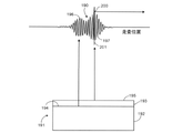
図1は、低コヒーレンス干渉計から取得された低コヒーレンス干渉信号150の一例を示すプロットである。低コヒーレンス干渉信号150は、物体の単一の点、例えば単一の反射性界面を有するシリコン・ウェハの点から取得された複数の検出強度値を含む。強度値は、物点(object point)から反射された光と干渉計の参照物体から反射された光との間の光路長差(optical path length difference : OPD)の関数として変化する。干渉信号150は、OPDを走査することによって、例えば、光学部品および/または物体を移動させて、物体から反射する光又は参照光が進む光路を変えることによって得られる低コヒーレンス走査光干渉(coherence scanning light interferometry : CSI)信号である。
FIG. 1 is a plot showing an example of a low
図1では、強度値は、OPDの変化に相関する関数走査位置としてプロットされ、複数のフリンジ(fringe)152を有する干渉パターン151をマッピングする。フリンジ152は、低コヒーレンス包絡線(low coherence envelope)154に従って最大値の両側で減衰している。低コヒーレンス包絡線がない場合には、干渉パターンのフリンジは通常、広範囲の光路差にわたって同様の振幅を有する。低コヒーレンス包絡線154自体は、そのような干渉信号内には明確に現れることはないが、説明のために示されている。OPD軸に沿った干渉パターンの場所は、一般的に、ゼロ(zero)OPDの位置、例えば、物体の点から反射された光と参照物体から反射された光との間のゼロOPDに対応する走査位置または空間位置に関連付けられる。ゼロOPD走査位置は、各物点の相対的な高さ、および干渉計に対する各物点の位置に影響を与える物体自体の方向および位置を表す物体トポグラフィー(object topography)の関数である。いくつかの実施形態では、干渉信号はまた、材料の介在層によって生じる分散および吸収等の試験試料に関連する寄与を含む。
In FIG. 1, intensity values are plotted as a function of scan position correlated to changes in OPD, mapping an
フリンジ152の振幅を変調する低コヒーレンス包絡線154の幅は、一般的に、検出された光のコヒーレンス長に対応する。コヒーレンス長を決定する要因の中には、たとえば、光源のスペクトル・バンド幅に関係付けられる時間コヒーレンス現象と、たとえば、物体を照明する光の入射角度の範囲に関係付けられる空間コヒーレンス現象がある。典型的には、コヒーレンス長は次の場合に減少する:(a)光源のスペクトル・バンド幅が大きくなる、および/または(b)入射角度の範囲が大きくなる。データを取得するために用いられる干渉計の構成に応じて、これらのコヒーレンス現象の一方もしくは他方が優勢になってもよく、またはそれらが両方とも全体のコヒーレンス長に実質的に寄与してもよい。干渉計のコヒーレンス長は、例えば、薄膜構造ではなく、単一の反射表面を有する物体から干渉信号を取得することによって決定されることができる。コヒーレンス長は、観察された干渉パターンを変調する包絡線の半値幅として表されることができる。
The width of
図1から分かるように、干渉信号150は、コヒーレンス包絡線の幅よりも大きく、従って、検出された光のコヒーレンス長よりも大きく変化する光路差の範囲を有する光を検出した結果として生成される。概して、低コヒーレンス干渉信号は、検出された光のコヒーレンス包絡線によって振幅変調された複数の干渉フリンジを得た結果として生成される。例えば、干渉パターンは、観察される複数の干渉フリンジの振幅が互いに対して少なくとも20%、少なくとも30%または少なくとも50%だけ異なるOPDの範囲にわたって取得されてもよい。例えば、フリンジ98は、フリンジ99の最大振幅よりも約50%小さい最大振幅を有する。
As can be seen in FIG. 1,
低コヒーレンス干渉計は、干渉計のコヒーレンス長に匹敵するかまたはそれよりも長いOPDの範囲にわたって干渉信号を検出するように構成されることができる。例えば、検出されるOPDの範囲は、コヒーレンス長よりも少なくとも2倍大きくてもよい(例えば、コヒーレンス長よりも約3倍以上、約5倍以上、約10倍以上、約50倍以上、または約100倍以上大きい)。いくつかの実施形態では、検出された光のコヒーレンス長は、物体の特徴の高さ変化のオーダーであり、例えば、数ミクロン以下だが検出された光の公称上の波長よりも大きいオーダーである。 Low coherence interferometers can be configured to detect interfering signals over a range of OPDs that are comparable to or longer than the coherence length of the interferometer. For example, the range of OPD detected may be at least 2 times greater than the coherence length (e.g., about 3 times greater, about 5 times greater, about 10 times greater, about 50 times greater, or about 50 times greater than the coherence length). 100 times larger). In some embodiments, the coherence length of the detected light is on the order of the height variation of the object feature, eg, on the order of a few microns or less but greater than the nominal wavelength of the detected light.
図2は、物体191から取得された例示的な干渉信号190を示す概略図であり、基板192およびその上にある層、例えば薄膜(thin film)193を含む。基板192および薄膜193によってそれらの間に界面194が規定される。薄膜193の外面195によって、物体とその周囲、例えば、空気、他のガス、または真空との間の界面が規定される。複数の界面は一般的に、物体の部分間の屈折率の変化によって規定される。物体は、他の層の中でも、複数の薄膜を含んでもよい。
FIG. 2 is a schematic diagram illustrating an
干渉信号190は、界面194から生じる第1の干渉パターン196および界面195から生じる第2の干渉パターン197を含む。第1の干渉パターン196と第2の干渉パターン197は重なり合っている。たとえば、干渉パターン(196、197)の最大値は、干渉計のコヒーレンス長よりも短いOPDだけ離され、パターン(196、197)はゼロ強度の領域によって離されていない。重なり合う干渉パターンは互いに歪め合うため、重なり合う干渉パターンは誤った結果をもたらす可能性がある。
低コヒーレンス走査干渉計として構成できる干渉計の複数の例には、マイケルソン(Michelson)、リンニク(Linnik)およびミラウ(Mirau)干渉計が含まれるが、これらに限定されない。図3は、マイケルソン型の走査干渉計を示す。ここでは、光源モジュール205は、照明光206をビームスプリッタ208に供給し、ビームスプリッタ208は、それをミラウ干渉対物レンズアセンブリ210に向ける。照明光206は、所望のコヒーレンス長を生成するスペクトル特性を有する広帯域光源(例えば、連続広帯域光源)からの広帯域光(例えば、白色光)を含み得る。広帯域光源の例は、特に、発光ダイオード、ハロゲンランプ、アーク(arc)、ランプ、超発光ダイオード(super luminescent diodes)または白熱光源を含むが、これらに限定されない。アセンブリ210は、対物レンズ211と、参照ミラー215を規定するその小さな中央部分に反射コーティングを有する参照平面(reference flat)212と、ビームスプリッタ213と、を含む。動作中、対物レンズ211は、参照平面212を介して試験試料220に向けて照明光を集束させる。ビームスプリッタ213は、集束光の第1の部分を参照ミラー215に反射して参照光222を規定し、集束光の第2の部分を試験試料220に透過して測定光224を規定する。次に、ビームスプリッタ213は、試験試料220から反射(または散乱)された測定光を、参照ミラー215から反射された参照光と再合成させ、対物レンズ211および結像レンズ230は、合成された光を結像して検出器(例えば、多画素カメラ)240上で干渉させる。検出器からの1つまたは複数の測定信号は、コンピュータ(図示せず)に送られる。
Examples of interferometers that can be configured as low coherence scanning interferometers include, but are not limited to, Michelson, Linnik and Mirau interferometers. FIG. 3 shows a scanning interferometer of the Michelson type. Here,
図3の実施形態における走査は、ミラウ干渉対物レンズアセンブリ210に結合された圧電トランスデューサ(piezoelectric transducer : PZT)260を含み、この圧電トランスデューサは、カメラの各画素における走査干渉データを提供するために(例えば、I(ζ、h)、ここで、Iは信号強度を表す干渉データであり、ζは物体表面に直交する干渉計走査座標であり、hは表面高さである)、対物レンズ211の光軸に沿って試験試料220に対してアセンブリ210全体を走査するように構成される。代替的には、PZTアクチュエータ270によって示されるように、PZTは、アセンブリ210ではなく試験試料に連結されて(coupled)、それらの間の相対移動を提供してもよい。特定の実施形態では、走査は、対物レンズ211の光軸に沿って参照ミラー215およびビームスプリッタ213の一方または両方を対物レンズ211に対して移動させることによって提供され得る。
Scanning in the embodiment of FIG. 3 includes a piezoelectric transducer (PZT) 260 coupled to the Mirau interference
光源モジュール205は、空間的に拡大される光源(spatially extended source)201と、レンズ202および203によって形成される望遠鏡(telescope)と、(レンズ203の後部焦点面と一致する)レンズ202の前部焦点面に配置された絞り(stop)204と、を含む。この構成は、ケーラー撮像(Koehler imaging)の一例であるミラウ干渉対物レンズアセンブリ210の瞳面245に空間的に拡大される光源を結像する。絞り204のサイズは、試験試料220上の照明野(illumination field)のサイズを制御する。いくつかの実施形態では、光源モジュールは、空間的に拡大される光源が、クリティカル撮像(critical imaging)として知られる試験試料上に直接結像される構成を含み得る。どちらのタイプの光源モジュールも、リンニク型走査干渉分光システムなどの他のタイプの干渉計を用いて使用されてもよい。
図4は、本明細書において開示される干渉計などの走査干渉計を使用して分析されるデバイス300の一例を示す概略図である。デバイス300は、例えば、ユーザの眼の前に配置されたときに、AR/VRデバイスの周辺部(periphery)から画像光情報を運び、正常な視覚を妨げることなくデータまたは画像のオーバーレイを生成するために眼に光を向ける導波路構造として人工現実(artificial reality : AR)/仮想現実(virtual reality : VR)デバイスにおいて使用されてもよい。本明細書では試験試料とも呼称されるデバイス300は、スタック内に配置された複数の層を含む。この例では、複数の層は、プレート(plate)302、304、306、308を含む。第1のプレート302は、上部第1表面314および下部第2表面320を含み得る。同様に、第2のプレート304は、上部第1表面322および下部第2表面324を含み、第3のプレート306は、上部第1表面326および下部第2表面328を含み、第4のプレート308は、上部第1表面330および下部第2表面332を含み得る。図4には4つのプレートが示されているが、より多いかまたはより少ない数のプレートがデバイス300内に配置されてもよい。プレートは、試料保持部312によって定位置に保持される。スタック内の1つ以上のプレートは、対応するギャップ(gap)(例えば、ギャップ310)によってスタック内の隣接するプレートから離間されてもよい。1つ以上のプレートのスタックはまた、スタックのいずれかの端に、またはスタック全体において個別のプレート上に形成された回折光学素子および/またはコーティング(coating)(図示せず)を含み得る。回折光学素子は、光を個別のプレートに結合する、および/または個別のプレートから結合する光カプラ(optical couplers)(例えば、ホログラフィック入力および出力カプラ(holographic input and out couplers))として用いられ、次に、光を移動させるための導波路として用いれれてもよい。
FIG. 4 is a schematic diagram illustrating an example of a
いくつかの実装形態では、例えば、AR/VR用途では、デバイス300内の複数のプレートの平行度を特定および制御すること、ならびに、複数のプレートのうちの1つ以上の表面の平面度、複数のプレートのうちの1つ以上の表面粗さ、およびプレート間の距離(例えば、ギャップ厚)などの他のデバイス特性を測定および制御することが有用であり得る。CSIには、デバイス300などのスタックされたデバイスを測定するための計測技術としていくつかの利点がある。たとえば、CSIは連続広帯域光源(例えば、発光ダイオード、ハロゲンランプ、白熱光源)の使用に依存することが多いため、光学フィルタなどの標準的な光学コンポーネントを使用して入射光スペクトルを調整することは容易である。さらに、CSIにおいて、広帯域スペクトルは、ギャップによって離間された層を有する光デバイスにおいて特に懸念される光路差が光源のコヒーレンス長を超えるキャビティからの干渉を自然に抑制する。
In some implementations, for example, in AR/VR applications, specifying and controlling the parallelism of multiple plates in
それにもかかわらず、CSIを使用して、デバイス300のようなギャップによって離間された複数の層を有する光学デバイスの表面トポグラフィーを測定することは、いくつかの理由から困難である可能性がある。例えば、界面が互いに近い場合、界面が近いことによって重なり合う干渉パターンが生成されて、干渉信号の歪みが生じることがある。場合によっては、複数の介在層(intervening layers)によって、信号分散および吸収の量が増加する。たとえば、複数のガラスプレートの比較的大きなスタックでは、吸収と散乱によって光が損失して、干渉信号内のピークの振幅を減衰させる。いくつかの場合では、分散は、スタック組立工程と同様に、適用された表面特徴および/またはコーティングから生じる応力(stresses)の結果であり得る。例えば、いくつかの実施態様では、複数のガラスは、ホログラフィック入出力カプラでコーティングされ、アセンブリに接着され、そのすべてによって、複数のプレートが曲げられ、場合によっては互いに接触されることさえあり得る。このような効果によって生じる分散は、測定された信号において位相遅延として現れることがある。分散が非線形である場合、正味の効果は、フリンジコントラストの損失および低コヒーレンス信号におけるコヒーレンス包絡線の広がりであり得る。複数の層のスタックが厚いほど、干渉計がスタック内をより深く走査するにつれて、分散の影響が悪化する。前述した信号非線形性は、スタック内のすべての介在層からの分散および表面特徴からの分散特性に依存し、そのような情報は、測定を実行する前には知ることができない可能性があるため、非線形性を補償するためにあらゆる種類の事前較正を実行することは困難である。
Nevertheless, using CSI to measure the surface topography of optical devices having multiple layers separated by gaps, such as
本開示は、分散および/または干渉信号に対する他の悪影響をもたらす非線形性を補償しながら、そのような多層スタックの計測を実行する技術およびシステムに関する。概して、特定の態様では、本開示は、1)多層スタックを有する試験試料から得られた試料干渉データを周波数領域に変換すること、2)周波数領域の試料干渉データから非線形位相変化を特定すること(非線形位相変化は、試験試料によって測定ビームに導入された分散の結果である)、および3)特定された非線形位相変化を周波数領域の試料干渉データから除去して補償された干渉データを生成することを含む技術をカバーする。次いで、補償された干渉データは、時間領域に再び変換され、そこから表面トポグラフィー及び表面分離などの試験試料に関する情報が抽出されることができる。代替的にはまたは追加的には、計測データは、時間領域に変換して戻す前に、補償された干渉データから抽出されてもよい。 The present disclosure relates to techniques and systems for performing metrology of such multi-layer stacks while compensating for nonlinearities that result in dispersion and/or other adverse effects on interfering signals. In general, in certain aspects, the present disclosure includes 1) transforming sample interferometry data obtained from a test sample having a multilayer stack into the frequency domain, 2) identifying nonlinear phase changes from the frequency domain sample interferometry data. (the nonlinear phase changes are the result of dispersion introduced into the measurement beam by the test sample); and 3) removing the identified nonlinear phase changes from the frequency domain sample interferometric data to produce compensated interferometric data. Covers techniques including The compensated interference data is then transformed back to the time domain from which information about the test sample such as surface topography and surface separation can be extracted. Alternatively or additionally, the metrology data may be extracted from the compensated interference data before converting back to the time domain.
図5は、図3のミラウ干渉計などのCSI干渉計を使用して、デバイス300などの多層スタックを有する光学デバイスの表面トポグラフィーを測定するためのプロセス(500)の一例を示すフローチャートである。本明細書で説明されるように、ミラウ干渉計の光源201は、比較的広い帯域幅(例えば、約100nm以上)を有する光源を含む広帯域光源とすることができ、例えば、発光ダイオード、ハロゲンランプ、アークランプ、白熱光源などを含み得る。例えば、光源は、電磁スペクトル(例えば、白色光)の可視部分にあってもよい。
FIG. 5 is a flowchart illustrating an example process (500) for measuring surface topography of an optical device having a multilayer stack, such as
光源201からの測定光は、例えばスタック内に配置された複数の層を有するデバイス300を含む試験試料220に入射するように、測定ビーム経路に沿って方向付けられる(502)。例えば、図4に示されるように、測定光316は、光軸318に沿ってデバイス300の第1の表面314に方向付けられる。光軸318は、デバイス300の第1の表面314に対して垂直であり得る。光316がデバイス300を通過するとき、光316の一部は、異なる屈折率の領域間の各界面で反射する。
Measurement light from
本明細書において説明されるように、デバイス300の複数の層は、測定光の1つまたは複数の波長に対して少なくとも半透過性(semi-transparent)を有するプレートを含み得る。例えば、戻ってくる光によって所望の計測性能を達成するためにノイズに対して十分な信号を有する干渉信号が生成されることができるように、使用される光は、吸収または散乱からの損失が十分に小さいプレート材料および表面を通過することができる。プレートは、例えば、ガラスプレートを含み得る。スタック内の1つ以上のプレートは、図3に示されるようにギャップによってスタック内の隣接するプレートから離間されてもよい。ギャップ厚(例えば、スタック内の2つの隣接するプレートの対向する表面間の平均距離)は、約数百ナノメートルから約数ミリメートル(例えば、少なくとも約100nmよりも大きい、少なくとも約1ミクロンよりも大きい、少なくとも約10ミクロンよりも大きい、少なくとも約100ミクロンよりも大きい、少なくとも約1ミリメートルよりも大きい)の間であってもよい。スタック内の1つまたは複数のプレートは、数百ミクロンから数十ミリメートルまたはそれ以上(例えば、少なくとも約100ミクロンよりも大きい、少なくとも約500ミクロンよりも大きい、少なくとも約1ミリメートルよりも大きい、少なくとも約5ミリメートルよりも大きい、少なくとも約10ミリメートルよりも大きい)の範囲の厚さを有してもよい。いくつかの実施態様では、複数のプレートは、1つまたは複数の異なる材料の単層または多層の薄膜(thin single- or multi-layer film)でコーティングされる。例えば、複数のプレートは、交互の屈折率を有する誘電体材料の単一膜または多層膜から形成された1つまたは複数の反射防止または高反射コーティングを含み得る。いくつかの実施態様では、プレートの表面は、特定の特徴を含むように改良される。例えば、プレートの表面は、エッチングされ、エンボス加工され、又はプレートの表面上に堆積された複数の格子(例えば、複数の回折格子)を使用するホログラフィック光カプラを含むように改良されてもよい。いくつかの実装形態では、プレートの第1の表面は第1の光カプラを含み、プレートの反対側の第2の表面は第2の光カプラを含む。光カプラは、光をプレート内に結合するか、プレートの外に結合するか、またはプレートの内外に結合するように用いられ得る。複数のプレートはそれぞれ、本明細書において記載されるような膜および/またはカプラを含み得る。
As described herein, multiple layers of
再び図3を参照すると、広帯域光源201からの光は、ビームスプリッタ213によって、1)参照ビーム経路の参照光222を規定するために参照ミラー215に集束される第1の部分と、2)測定ビーム経路の測定光224を規定するために試験試料220に集束される第2の部分とに分けられる。参照光222は、参照表面(例えば、参照フラット212)と接触するように参照ビーム経路に沿って方向付けされる(504)。そして、試験試料220から反射(又は散乱)された測定光は、参照ミラー215からの参照光と合成(506)されて出力光を形成する。結像レンズ230および対物レンズ211は、合成された光を結像して測定信号を生成するために複数の検出素子(例えば、多画素カメラ)を有する検出器アレイ240に干渉させる。幾つかの実装形態では、参照光及び測定光が等量のガラスを通過するようにビームスプリッタが製造されて、それによってコントラストの広がりに関連する分散を低減し得る。検出器からの1つまたは複数の測定信号は、コンピュータ(図示せず)に送られる。干渉は、2つの区間(leg)の光路の差が照明コヒーレンス長以内である場合に発生する。試験試料220の各表面から干渉を得るために、試験試料220の1つ以上の表面が順にコヒーレンス条件を満たすように、電動ステージを用いて、試験試料220および/または干渉計の構成要素が光軸318に沿って走査される(図4を参照)。
Referring again to FIG. 3, light from
検出器アレイから複数の干渉信号が試料干渉データを提供するために記録され(508)、検出器アレイでは、複数の干渉信号の各干渉信号が試験試料上の異なる位置に対応し、異なる検出素子によって記録される。例示的な測定において、試験試料220は、試験試料220の公称表面法線(nominal surface normal)を干渉計の光軸318に位置合わせする手段を提供する調整可能なマウント内に保持される。位置合わせプロセスは、例えば、試験試料表面および参照表面から検出器240の検出素子上に光源反射(source reflection)を結像することを含み得る。一旦位置合わせされると、電動ステージは、干渉計に最も近いスタック表面が物体空間焦点面(object space focus plane)のすぐ外側(及び右側に)になるように設定される。ステージは、カメラが干渉画像を取得している間、一定の速度で干渉計に向かって一部を移動させる。各表面が等しい経路領域を通過するとき、干渉が生じ、カメラは、例えば、2つの波面からの干渉によって生成される面強度パターン(areal intensity pattern)を含むインターフェログラム(interferograms)を記録する。干渉計は、参照区間と試験区間との間の等しい光路条件を満たす物体面での最良のフォーカスが生じるように構成されてもよい。
A plurality of interference signals are recorded 508 from the detector array to provide sample interference data, where each interference signal of the plurality of interference signals corresponds to a different location on the test sample and a different detector element. recorded by In an exemplary measurement,
インターフェログラムは、様々なステージ位置で検出器によって取得されて1つ以上の電子プロセッサ(図示せず)に提供され(510)、続いて、1つ以上の電子プロセッサは、干渉信号に対して分散補償を実行し(512)、ピークコヒーレンスコントラスト検出方法(peak-coherence contrast detection methods)、最小二乗テンプレート分析(least-squares template analysis)、または周波数領域分析などのCSI方法を使用して補正された干渉信号を処理する。表面トポグラフィー分析を実行するためのCSI方法に関するさらなる情報は、例えば、米国特許第5,398,113号明細書、米国特許第5,953,124号明細書、米国特許第8,045,175号明細書および米国特許第7,522,288号明細書において見出され、これらの各々は、その全体が参照により本明細書に組み込まれる。例えば、走査速度、カメラ速度、および照明光の平均波長が既知であると仮定すると、各表面からのインターフェログラムを分析して、表面トポグラフィーを取得することができる。その取得が走査全体でインターフェログラムを継続的に取得する場合、すべての表面間の関係情報が保持されることができる。 Interferograms are acquired by detectors at various stage positions and provided 510 to one or more electronic processors (not shown), which in turn process the interferograms into Dispersion compensation is performed 512 and corrected using CSI methods such as peak-coherence contrast detection methods, least-squares template analysis, or frequency domain analysis. Handle interfering signals. Further information regarding CSI methods for performing surface topography analysis can be found, for example, in US Pat. No. 5,398,113, US Pat. No. 5,953,124, US Pat. and US Pat. No. 7,522,288, each of which is hereby incorporated by reference in its entirety. For example, the interferogram from each surface can be analyzed to obtain the surface topography, assuming the scan speed, camera speed, and average wavelength of the illuminating light are known. If the acquisition acquires the interferogram continuously throughout the scan, the relationship information between all surfaces can be retained.
図6は、インターフェログラムの形状に影響を与える試験試料によって引き起こされる分散および他の影響を補償するために1つまたは複数のプロセッサによって実行され得る例示的なプロセス(600)を示すフローチャートである。第1のステップ(602)では、干渉計システムの1つまたは複数のプロセッサが、試料干渉測定データを時間領域から周波数領域に変換する。 FIG. 6 is a flowchart illustrating an exemplary process (600) that may be performed by one or more processors to compensate for test sample induced dispersion and other effects that affect the shape of an interferogram. . In a first step (602), one or more processors of the interferometer system transform the sample interferometric data from the time domain to the frequency domain.
たとえば、理論に縛られることを望まない場合、離散的にサンプリングされた低コヒーレンス干渉信号Iは、以下のように周波数Kの範囲にわたる干渉パターンのインコヒーレント合計(incoherent sum)として表されることができる。 For example, without wishing to be bound by theory, a discretely sampled low coherence interference signal I can be expressed as the incoherent sum of the interference pattern over a range of frequencies K as can.


いくつかの場合では、干渉データを周波数領域に変換する前に、干渉データからDC成分が除去される。代替的にはまたは追加的には、試験試料の選択された表面に対応する複数の干渉信号は、それらが十分に離間されている場合に分離される。それらが分散に起因して時間領域において十分に分離されない場合、及び両方の表面で経験される分散が名目上同じである場合、分散補償は、時間領域分離を改善するために実行されることができる。一例として、所定の値を超える信号強度を有する干渉データからの干渉信号は、試験試料の選択された表面の界面に対応するものとして特定され得る。所定の値よりも大きい(またはそれ以上の)信号強度を有する干渉信号は、他の残りの干渉信号の値をゼロに設定することによって分離されることができる。代替的にはまたは追加的には、時間領域の干渉信号(例えば、分離された干渉信号)は、それらを周波数領域に変換する前に時間シフトされてもよい。例えば、各画素について、時間領域の信号データは、信号のピーク振幅がデータセットの最初に存在するように時間シフトされてもよい。これは、例えば、信号の一方の側から除去されたデータが信号の他方の側にコピーされる循環バッファ(circular buffer)(またはリングシフトレジスタ)技術を使用して達成されることができる。これにより、フーリエ成分の線形位相項(linear phase term)が除去される。 In some cases, the DC component is removed from the interferometric data prior to transforming the interferometric data into the frequency domain. Alternatively or additionally, multiple interfering signals corresponding to selected surfaces of the test sample are separated if they are sufficiently spaced apart. If they are not sufficiently separated in the time domain due to dispersion, and if the dispersion experienced by both surfaces is nominally the same, dispersion compensation may be performed to improve the time domain separation. can. As an example, interferometric signals from interferometric data having signal intensities exceeding a predetermined value can be identified as corresponding to selected surface interfaces of the test sample. Interfering signals with signal strength greater than (or greater than) a predetermined value can be isolated by setting the values of other remaining interfering signals to zero. Alternatively or additionally, the time-domain interfering signals (eg, the separated interfering signals) may be time-shifted before transforming them to the frequency domain. For example, for each pixel, the time-domain signal data may be time-shifted such that the peak amplitude of the signal is at the beginning of the data set. This can be accomplished, for example, using a circular buffer (or ring shift register) technique in which data removed from one side of the signal is copied to the other side of the signal. This removes the linear phase term of the Fourier component.
試料干渉データの周波数領域への変換に続いて、非線形位相変化が、周波数領域の試料干渉データから特定される(604)。本明細書において記載されるように、非線形位相変化は、試験試料の上または内部の複数の層および/または表面特徴によって測定ビームに導入された分散の結果であり得る。非線形位相変化の特定は、較正情報または試験試料の予測される特性からではなく、試料干渉データ自体から非線形位相変化を導出することを含む。非線形位相変化を特定することは、例えば、周波数領域における複数の干渉信号の少なくとも一部分の位相変化を取得すること(606)を含み得る。分散が空間的に独立であるか、または分散が空間的に独立であると仮定することができる場合、単一の検出素子または複数の検出素子からの干渉信号は、分散が一定であると予想される領域において測定された位相ノイズを低減するのに十分であり得る。分散の空間的独立性が仮定できない場合、分散は、各画素について個別に評価される。 Following transformation of the sample interferometric data to the frequency domain, nonlinear phase changes are identified from the frequency domain sample interferometric data (604). As described herein, nonlinear phase changes can be the result of dispersion introduced into the measurement beam by multiple layers and/or surface features on or within the test sample. Determining the nonlinear phase change involves deriving the nonlinear phase change from the sample interferometric data itself, rather than from calibration information or expected properties of the test sample. Identifying non-linear phase changes may include obtaining phase changes of at least a portion of the plurality of interfering signals in the frequency domain (606), for example. If the dispersions are spatially independent or can be assumed to be spatially independent, the interfering signal from a single detector element or multiple detectors is expected to have constant dispersion. may be sufficient to reduce the measured phase noise in the region where If the spatial independence of the variances cannot be assumed, the variances are evaluated individually for each pixel.
一例として、フーリエ変換されたデータにおける有用な情報の大部分は、フーリエ係数の相対的な大きさが大きい領域に含まれ得る。従って、複数の干渉信号の少なくとも一部分の位相変化を取得すること(606)は、1つまたは複数のプロセッサを用いて、十分に高い振幅を有する複数のフーリエ成分の一部分の位相を計算し、アンラップする(unwrap)こと、例えば、少なくとも所定の信号対雑音(signal to noise : S/N)比を有する波数においてフーリエ成分を選択することを含み得る。S/N比の選択は、記録されたデータに依存する。ノイズの多いデータ領域は、平均化または後処理と組み合わせて、ドロップアウト(測定されていないポイント)を回避するために低いS/N比を必要とする場合がある。クリーンなデータ領域は、許容可能な測定値を提供するために、より高いS/N比のみを必要とする場合がある。例えば、幾つかの実装形態では、許容可能な精度を有する非線形(分散)位相項は、「2」未満のフーリエ成分S/N比を使用して測定され得る。代替的には、幾つかの実装形態では、S/N比は「5」よりも大きくてもよい。試料干渉データからの位相変化は、低コヒーレンス撮像干渉計システムによって観察される波数の範囲にわたって特定され得る。有効範囲は、照明スペクトル帯域幅に依存する。例えば、より大きな帯域幅は、より大きな範囲を提供し得る。いくつかの実施態様では、位相変化を取得すること(606)は、複数の干渉信号の少なくとも一部分の平均(例えば、平均(mean)、モード(mode)、中央値(median))位相変化を導出することを含む。いくつかの実施態様では、位相変化は、(例えば、検出器の複数の画素素子にわたる)領域内の各位置について個別にかつ独立して導出されることができる。しかし、複数の位置を平均化することは、分散が領域全体で均一である場合に、測定誤差を低減するための有用な方法であり得る。干渉データ内の位相情報の評価に関する追加情報は、例えば、米国特許第5,398,113号明細書(例えば、9:44-10:54)及び米国特許第7,522,288号明細書(例えば、11:49-13:12)において見出され、これらの各々は、その全体が参照により本明細書に組み込まれる。 As an example, most of the useful information in Fourier transformed data may be contained in regions where the relative magnitudes of the Fourier coefficients are large. Accordingly, obtaining (606) the phase change of at least a portion of the plurality of interfering signals includes calculating, using one or more processors, the phase of a portion of the plurality of Fourier components having sufficiently high amplitude and unwrapping the unwrapping, eg, selecting Fourier components at wavenumbers having at least a predetermined signal to noise (S/N) ratio. The choice of S/N ratio depends on the recorded data. Noisy data regions may require low signal-to-noise ratios to avoid dropouts (unmeasured points) in combination with averaging or post-processing. Clean data areas may require only a higher S/N ratio to provide acceptable measurements. For example, in some implementations, nonlinear (dispersive) phase terms with acceptable accuracy can be measured using a Fourier component S/N ratio of less than '2'. Alternatively, in some implementations, the S/N ratio may be greater than '5'. Phase changes from sample interferometry data can be identified over the range of wavenumbers observed by a low-coherence imaging interferometer system. Effective range depends on illumination spectral bandwidth. For example, larger bandwidths may provide greater range. In some implementations, obtaining the phase change (606) derives a mean (e.g., mean, mode, median) phase change of at least a portion of the plurality of interfering signals. including doing In some implementations, the phase change can be derived separately and independently for each location in the area (eg, across multiple pixel elements of the detector). However, averaging over multiple locations can be a useful method for reducing measurement error if the variance is uniform across the region. Additional information on evaluating phase information in interferometric data can be found, for example, in US Pat. No. 5,398,113 (eg, 9:44-10:54) and US Pat. 11:49-13:12), each of which is incorporated herein by reference in its entirety.
非線形位相変化を特定することは、さらに、位相変化にフィットする(fit)関数を取得すること(608)を含み得る。例えば、上記で説明されたように、選択された波数に対する平均位相変化は、領域内の全ての画素又は一部分の画素に対して導出され得る。いくつかの実施態様では、複数の非線形位相変化が、試料表面全体における複数の領域について取得される。例えば、選択された波数にわたって複数の平均位相変化が導出されることができ、各平均は、試料表面の異なるそれぞれの領域に対応する異なる一部分の画素から導出される。幾つかの実装形態では、選択された波数は、対応する位相変化が導出される領域毎に異なることがある。材料の介在層によっておよび/または試験試料に誘起された応力によって引き起こされる分散は、多くの場合、二次位相(quadratic phase)の非線形性をもたらす場合がある。したがって、位相変化にフィットする関数(function)は、x2のような2次形式を有し得る。しかしながら、非線形位相変化は、2次以外の形式を有しても良い。さらに、「2」よりも大きい次数の多項式を有する関数、指数関数、対数関数、スプラインフィッティング(spline fits)、ガウスフィッティング(Gaussian fits)などのような他の関数を位相変化にフィッティングさせてもよい。 Identifying non-linear phase changes may further include obtaining a function to fit the phase changes (608). For example, as explained above, the average phase change for a selected wavenumber can be derived for all or a subset of pixels within a region. In some embodiments, multiple nonlinear phase changes are acquired for multiple regions across the sample surface. For example, a plurality of average phase changes can be derived over a selected wavenumber, each average derived from a different fraction of pixels corresponding to a different respective region of the sample surface. In some implementations, the selected wavenumber may be different for each region from which the corresponding phase change is derived. Dispersion caused by intervening layers of material and/or by stress induced in the test sample can often lead to quadratic phase nonlinearities. Therefore, a function that fits the phase change can have a quadratic form such as x2. However, the nonlinear phase change may have forms other than quadratic. In addition, other functions such as functions with polynomials of degree greater than "2", exponential functions, logarithmic functions, spline fits, Gaussian fits, etc. may be fitted to the phase change. .
非線形位相変化の特定に続いて、周波数領域における試料干渉データから特定された非線形位相変化が除去されて(610)、補償された干渉計データを生成する。例えば、特定された非線形位相変化を除去すること(610)は、各画素または一部分の画素について、試料干渉データからフィッティングされた関数データ(例えば、最良フィッティング)を取り除くことを含み得る。幾つかの実装形態では、特定された非線形位相情報がさらに分析されて、例えば(材料の屈折率は波数の非線形関数であるので)群速度屈折率(group-velocity refractive index)及び/又は層材料が既知の場合の厚さのような材料特性、並びに例えば吸収及び分散に影響する汚染物質のような材料欠陥を含む有用な情報を提供してもよい。 Following identification of the nonlinear phase changes, the identified nonlinear phase changes are removed 610 from the sample interferometric data in the frequency domain to produce compensated interferometer data. For example, removing 610 the identified nonlinear phase changes may include removing the fitted function data (eg, best fit) from the sample interferometric data for each pixel or subset of pixels. In some implementations, the identified nonlinear phase information is further analyzed, e.g., group-velocity refractive index and/or layer material It may provide useful information including material properties such as thickness when λ is known, and material imperfections such as contaminants that affect absorption and dispersion.
非線形位相変化を除去した後、補償された試料干渉データを時間領域に戻すように変換し得る(612)。次いで、1つまたは複数のプロセッサは、本明細書において開示されるように、CSI方法を使用して表面のトポグラフィーマップ(topographical maps)などの計測情報を提供するために、補償されたインターフェログラムを処理し得る。CSIデータを使用してトポグラフィーマップを作成するための技術のさらなる例は、例えば、米国特許第5,953,124号明細書および米国特許第7,522,288号明細書において見出され、これらの各々は、その全体が参照により本明細書に組み込まれる。このように、干渉信号データ自体を用いて試験試料からの干渉信号への分散寄与を評価するので、介在物質に関する事前の知識(例えば、屈折率、分散特性または層の厚さ)は不要である。代替的にはまたは追加的には、トポグラフィーマップを含む計測情報は、(例えば、米国特許第5,398,113号明細書に記載されているもののようなものであり、その内容は、その全体が参照により本明細書に組み込まれる)周波数領域法を使用して、周波数領域における補償された干渉計データから導出されることができる。現在の実装形態では、分散特性は領域全体で同じであると仮定しているが、非線形項(例えば二次項)を領域の位置の関数として評価することによって、この手段は領域依存分散に拡張されることができる。 After removing the nonlinear phase changes, the compensated sample interferometric data may be transformed back to the time domain (612). The one or more processors then process the compensated interferometer to provide metrology information, such as topographical maps of the surface using CSI methods, as disclosed herein. gram can be processed. Further examples of techniques for creating topography maps using CSI data can be found, for example, in US Pat. Nos. 5,953,124 and 7,522,288, each of which is incorporated herein by reference in its entirety. In this way, the interference signal data itself is used to estimate the dispersive contribution to the interference signal from the test sample, so no prior knowledge of the intervening material (e.g. refractive index, dispersive properties or layer thickness) is required. . Alternatively or additionally, the metrology information comprising the topography map is such as that described in U.S. Pat. No. 5,398,113, the contents of which are can be derived from the compensated interferometer data in the frequency domain using frequency domain methods, which are incorporated herein by reference in their entirety. Although the current implementation assumes that the dispersion properties are the same across regions, this measure is extended to region-dependent dispersion by evaluating nonlinear terms (e.g., quadratic terms) as a function of region position. can
一実施形態では、プロセッサは、補償された干渉データから、試験試料内の第1の界面と第2の界面との間の距離を決定することができる。第1の界面と第2の界面との間の距離を決定することは、例えば、補償された複数の干渉信号のうちの補償された各干渉信号について、試験試料における第1の界面(例えば、デバイス300の界面314,320,322,324,326,328,330または332のいずれか)に対応する第1の干渉パターンの第1の強度ピーク、および試験試料における異なる第2の界面(例えば、デバイス300のインターフェース314,320,322,324,326,328,330または332のいずれか)に対応する第2の干渉パターンの第2の強度ピークを特定することを含み得る。次いで、複数の干渉信号の補償された各干渉信号について、1つまたは複数のプロセッサは、第1の干渉パターンの特定された第1の強度ピークが生じる位置と、第2の干渉パターンの特定された第2の強度ピークが生じる位置との間の間隔を導出し得る。各信号は、界面に沿った異なる位置に対応する異なる検出素子(例えば、画素)から得られるので、その間隔は、第1の界面と第2の界面との間の平均距離を提供するために、異なる信号間で平均化され得る。この距離は、例えば、試験試料内の層間の平均ギャップ厚に対応し得る。例えば、距離は、試験試料内の第1のプレートと第2のプレートとの間の平均ギャップ厚であり得る(例えば、デバイス300におけるプレート302とプレート304との間のギャップ距離、デバイス300におけるプレート304とプレート306との間のギャップ距離、デバイス300におけるプレート306とプレート308との間のギャップ距離)。代替的には、距離は、試験試料内のプレート上に形成された層の平均厚さに対応し得る。例えば、距離は、試験試料内のプレートの表面上に形成された薄膜誘電体層の厚さに対応し得る。代替的には、距離は、試験試料内のプレートの厚さ(例えば、デバイス300のプレート302、304、306または308の厚さ)に対応し得る。
In one embodiment, the processor can determine the distance between the first interface and the second interface within the test sample from the compensated interference data. Determining the distance between the first interface and the second interface includes, for example, the first interface (e.g., A first intensity peak in a first interference pattern corresponding to an
いくつかの実装形態では、1つまたは複数のプロセッサは、補償された各干渉信号について導出された間隔に基づいて、第1の界面と第2の界面との間の平行度のレベルを決定し得る。例えば、1つ又は複数のプロセッサが使用されて、試験試料内の2つのプレート間のギャップ厚(例えば、デバイス300に示される複数のギャップ310のいずれか)がギャップ全体でどのように均一であるか又は不均一であるかを示すトポグラフィーマップとして、各検出素子(例えば、画素)の距離データを出力する。例えば、トポグラフィーマップは、第1および第2の界面の3次元表面トポグラフィー(areal surface topographies)の違いを示し得る。トポグラフィーマップはディスプレイに出力されてもよい。いくつかの実施態様では、1つ以上のプロセッサは、トポグラフィーマップから他の情報、例えば、第1の界面と第2の界面との間の二乗平均平方根差(root-mean-square difference)、第1の界面と第2の界面との間のピークと谷との差(peak-valley difference)、またはトポグラフィーマップの任意の他のパラメータ化を決定するように構成される。いくつかの実装形態において、1つまたは複数のプロセッサは、試験試料内の1つまたは複数の界面(例えば、デバイス300の界面314,320,322,324,326,328,330または332のいずれか)の平面度のレベルを決定することができる。例えば、試験試料における界面の表面形態は、干渉計システムの参照平面に対して得られてもよい。
In some implementations, the one or more processors determine a level of parallelism between the first interface and the second interface based on the spacing derived for each compensated interference signal. obtain. For example, one or more processors are used to determine how the gap thickness between two plates in the test sample (eg, any of the
いくつかの実施形態では、本明細書において開示された技術を使用して取得されるデータの量は非常に大きく、特に、試験試料が、それらの間にギャップを有する複数の比較的厚いプレートを含むように構成される場合、取得するのにかなりの時間がかかる可能性がある。例えば、8枚の厚さ0.5mmのプレートから成り、プレート間の間隔が50ミクロンのスタックを有する試験試料の場合、スタック全体の物理的厚さは4.35mmである。カメラフレーム当たりの波長の1/8(フリンジの1/4)および500nmの平均光源波長に等しい走査方向に沿ったCSIサンプリングレートに対して、7万を超えるカメラフレームが、スタック全体を走査して全ての表面を取得するために必要である。各画像が8ビットでデジタル化された500x500画素であるとすると、これは約17.5GBのデータに相当する。さらに、100Hzで動作するカメラの場合、このプロセスは、約700秒(11.7分)を必要とする。 In some embodiments, the amount of data acquired using the techniques disclosed herein is very large, especially when the test sample comprises multiple relatively thick plates with gaps between them. If configured to do so, it can take a significant amount of time to retrieve. For example, for a test sample having a stack of eight 0.5 mm thick plates with 50 micron spacing between the plates, the physical thickness of the entire stack is 4.35 mm. Over 70,000 camera frames scanned the entire stack for a CSI sampling rate along the scan direction equal to 1/8 of the wavelength (1/4 of the fringe) per camera frame and an average source wavelength of 500 nm. Required to get all surfaces. Assuming each image is 500x500 pixels digitized at 8 bits, this corresponds to approximately 17.5 GB of data. Moreover, for a camera operating at 100 Hz, this process requires approximately 700 seconds (11.7 minutes).
いくつかの実装形態では、取得スループットは、スタック内の少なくとも1つの候補界面位置に関する情報を特定するために、より高い移動速度で初期高速走査(initial quick scan)を実行することによって増大され得る。試験試料内の少なくとも1つの候補界面位置に関する情報に基づいて、干渉計対物レンズおよび/または試験試料は、測定ビームの焦点面に隣接するスタックの少なくとも1つの候補界面を配置するように再配置されてもよい。次に、少なくとも1つの候補界面がより遅い速度で焦点面を通過し、及び/又は試料干渉データがより高い取得速度で取得されるように、干渉計対物レンズおよび/または試験試料を移動させることによって、より詳細な情報を得ることができる。 In some implementations, acquisition throughput may be increased by performing an initial quick scan at a higher travel speed to identify information about at least one candidate interface location within the stack. Based on the information regarding the location of the at least one candidate interface within the test sample, the interferometer objective and/or the test sample are repositioned to position the at least one candidate interface of the stack adjacent to the focal plane of the measurement beam. may Then, moving the interferometer objective and/or the test sample such that at least one candidate interface passes through the focal plane at a slower speed and/or sample interference data is acquired at a higher acquisition speed. You can get more detailed information by
例えば、幾つかの実装形態では、高速走査は、「サブナイキスト(Sub-Nyquist)」取得を用いて実行されてもよい。サブナイキスト取得は、典型的には、奇数整数倍(3、5、7、...)(サブナイキスト倍数)だけ標準CSI取得を超えてCSI走査速度および照明強度を増加させると同時に、カメラをシャッターして同じ逆数の倍数(1/3、1/5、1/7、...)だけフレームインテグレーション(frame integration)を減少させることを含む。その効果は、干渉をまばらにサンプリングすることにより、サブナイキスト倍数による取得時間とデータ量を削減しつつ、シャッターと強度の増加により干渉信号のコントラスト損失を最小限に抑えるというものである。このタイプの取得に対して支払われる代償は、状況によっては許容できるトレードオフである環境感度と測定ノイズの増加である。高速走査を実行することに関する追加情報は、例えば、米国特許第5,398,113号明細書及びHigh-speed non-contact profiler based on scanning white light interferometry, L. Deck and P. de Groot, Appl. Opt. 33(31), 7334-7338 (1994)において見出され、これらの各々は、その全体が参照により本明細書に組み込まれる。 For example, in some implementations, fast scanning may be performed using "Sub-Nyquist" acquisition. Sub-Nyquist acquisitions typically increase the CSI scan rate and illumination intensity over standard CSI acquisitions by odd integer multiples (3, 5, 7, . . . ) (sub-Nyquist multiples) while keeping the camera Including shuttering to reduce the frame integration by the same reciprocal multiple (1/3, 1/5, 1/7, ...). The effect is to reduce the acquisition time and data volume by sub-Nyquist multiples by sparsely sampling the interference, while minimizing the contrast loss of the interference signal by increasing the shutter and intensity. The price paid for this type of acquisition is increased environmental sensitivity and measurement noise, an acceptable trade-off in some circumstances. Additional information on performing high speed scans can be found, for example, in US Pat. No. 5,398,113 and High-speed non-contact profiler based on scanning white light interferometry, L. Deck and P. de Groot, Appl. Opt. 33(31), 7334-7338 (1994), each of which is incorporated herein by reference in its entirety.
高速初期走査を用いて得られたデータから、スタック内の少なくとも1つの候補界面位置が特定され得る。少なくとも1つの候補界面は、ピーク局所振幅を有する干渉信号の複数の部分の位置を特定することによって特定され得る。例えば、試験試料が、隣り合うプレート間にギャップを有する複数のプレートから構成され、プレート間のギャップ間隔を決定することに関心があるが、プレート表面に関する他の関連情報は関心がない場合、高速走査(例えば、サブナイキスト走査)を、最初に試験試料全体に実行して、全ての界面のステージ位置(stage location)を特定することができる。界面に対応するステージ位置は、振幅が極大に達する時間領域干渉信号内の位置に存在する。ほぼ予想されるプレートギャップ距離だけ離間された信号振幅の最大値は、プレートの候補表面として記録され得る。続いて、特定されたギャップを囲む複数の表面は、初期走査よりも遅い速度で(例えば、ナイキスト周波数以上の速度で)進行する標準的な走査を用いて測定され、スタック内の2つの異なるプレートの対向する表面をカバーする新たな干渉信号が記録されることができる。次に、本明細書において開示された分散補償技術は、新たに記録された信号に対して実行され、CSI分析は補正されたデータに適用されて2つの表面のより正確な位置を取得することができる。複数の走査表面が、干渉データが単一の取得走査によって取得されるほど十分に近い場合、ギャップ厚の変化は、複数の表面位置に対応する複数の走査位置間(すなわち、信号振幅の複数の局所ピーク(local peaks))の差分を差し引くことによって決定されてもよい。ピークが存在しないことが分かっている走査部分のrms変動が得られた場合、ピークを特定するために必要な振幅の大きさを推定することが可能である。rms変動は、「バックグラウンド(background)」の統計的特性の概念を提供する。ピークは、例えば、バックグラウンドを超える標準偏差のある特定された倍数でなければならない信号、例えば、「4」または「6」の値として定義され得る。 At least one candidate interface location within the stack may be identified from the data obtained using the fast initial scan. At least one candidate interface may be identified by locating portions of the interference signal having peak local amplitudes. For example, if the test sample consists of a plurality of plates with gaps between adjacent plates, and you are interested in determining the gap spacing between the plates, but are not interested in other relevant information about the plate surfaces, fast A scan (eg, a sub-Nyquist scan) can first be performed over the test sample to identify the stage locations of all interfaces. The stage position corresponding to the interface is the position within the time-domain interference signal where the amplitude reaches a maximum. The signal amplitude maxima spaced by approximately the expected plate gap distance can be recorded as the candidate surface of the plate. Multiple surfaces surrounding the identified gap are then measured using a standard scan that progresses at a slower speed than the initial scan (e.g., at or above the Nyquist frequency) and two different plates in the stack. A new interference signal can be recorded covering the opposing surface of the . The dispersion compensation techniques disclosed herein are then performed on the newly recorded signal and CSI analysis is applied to the corrected data to obtain more accurate positions of the two surfaces. can be done. If the multiple scan surfaces are close enough that the interferometric data is acquired with a single acquisition scan, then the change in gap thickness will be reflected between multiple scan locations corresponding to multiple surface locations (i.e., multiple may be determined by subtracting the difference of the local peaks. Given the rms variation of a scan portion that is known to be peak free, it is possible to estimate the magnitude of the amplitude needed to locate the peak. The rms variation provides the concept of a statistical property of "background". A peak can be defined, for example, as a signal that must be a certain specified multiple of standard deviations above background, eg, a value of “4” or “6”.
いくつかの実施態様では、候補表面のより正確な分析を行うことができるように、初期走査データは、候補表面の位置を迅速に特定するために用いられる。例えば、本明細書において記載されるような初期高速走査に続いて、特定された候補表面が干渉計システムの焦点面の近くに位置付けられるように、干渉計および/または試験試料を再配置することができる。この新しい位置から、初期走査よりも遅い速度で(例えば、ナイキスト周波数以上の速度で)進行する標準的な走査が実行されて、新しい干渉信号を記録し得る。次に、本明細書に開示された分散補償技術は、新たに記録された信号に対して実行され、CSI分析が補正されたデータに適用されて、候補表面に関する情報を取得して出力し得る。初期高速走査は、候補表面の最初の特定に使用されるものとして上述され、その後、候補表面の第2の走査が実行されて、より詳細な情報を得ることができる。しかしながら、いくつかの実施形態では、高速走査は、第2の追加走査を実行する必要なしに、候補表面に関する十分な詳細を提供してもよい。 In some implementations, the initial scan data is used to quickly locate the candidate surface so that a more accurate analysis of the candidate surface can be performed. For example, following an initial fast scan as described herein, repositioning the interferometer and/or the test sample so that the identified candidate surfaces are positioned near the focal plane of the interferometer system. can be done. From this new position, a standard scan, proceeding at a slower speed than the initial scan (eg, at or above the Nyquist frequency), may be performed to record the new interference signal. The dispersion compensation techniques disclosed herein may then be performed on the newly recorded signal and CSI analysis applied to the corrected data to obtain and output information about the candidate surface. . An initial fast scan is described above as being used to initially identify a candidate surface, after which a second scan of the candidate surface can be performed to obtain more detailed information. However, in some embodiments, a fast scan may provide sufficient detail about the candidate surface without having to perform a second additional scan.
代表的なアプリケーション
本明細書において記載された低コヒーレンス干渉測定方法およびシステムは、以下の表面分析問題のいずれかに使用されることができる:3次元表面トポグラフィー、テクスチャー測定(texture measurement)、表面形状測定、複数の表面の関係測定(厚さと平行度)、表面欠陥検出、簡単な薄膜;多層薄膜;層間のギャップを有するスタックされた多層物体;回折やその他の複雑な干渉効果を発生させる鋭いエッジや表面の特徴;未分解表面粗さ(unresolved surface roughness);例えば、他の点では平滑な表面上のサブ波長幅溝(sub-wavelength width groove)などの未分解表面特徴;異種材料;表面の偏光依存特性;干渉現象の入射角に依存した摂動(perturbation)をもたらす表面または変形可能な表面特徴の撓み(deflection)、振動または運動。薄膜の場合、関心のある可変パラメータは、膜厚、膜の屈折率、基板の屈折率、またはそれらの何らかの組み合わせであってもよい。次に、例示的なアプリケーションを説明する。
Exemplary Applications The low-coherence interferometric measurement methods and systems described herein can be used for any of the following surface analysis problems: three-dimensional surface topography, texture measurement, surface Form measurements, multi-surface relationship measurements (thickness and parallelism), surface defect detection, simple thin films; multi-layer thin films; stacked multi-layer objects with gaps between layers; edge or surface features; unresolved surface roughness; unresolved surface features such as sub-wavelength width grooves on an otherwise smooth surface; dissimilar materials; polarization dependent properties of ; deflection, vibration or motion of surfaces or deformable surface features that result in angle-of-incidence dependent perturbations of interference phenomena. For thin films, the variable parameter of interest may be the film thickness, the refractive index of the film, the refractive index of the substrate, or some combination thereof. An exemplary application will now be described.
AR/VR光学デバイス
本明細書において説明されるように、AR/VRアプリケーションは、複数の平行なプレートを含む複数のスタックを使用し、スタック内の平行なプレートは、デバイスがユーザの眼の前に配置されたときに、デバイスの周辺部からの光情報が眼に運ばれて、正常な視界を妨げることなくデータまたは画像のオーバーレイを生成するように、導波路として作用するように、それらの表面に適用される特徴およびコーティングを有する。高品質の画像を維持するには、特に、プレート間の良好な平行度を達成し、特定の表面が望ましい平面度を確保し、製造中にプレート間の特定の分離距離を維持することが重要である。いくつかの場合では、これらの光学デバイスに使用される複数のプレートは比較的厚く、干渉計の走査が光学プレートの奥深くまでプローブするために分散効果が生じる。
AR/VR Optical Devices As described herein, AR/VR applications use multiple stacks containing multiple parallel plates, and the parallel plates within the stacks allow the device to be positioned in front of the user's eye. They are designed to act as waveguides so that when placed in the eye, light information from the periphery of the device is carried to the eye to produce data or image overlays without interfering with normal vision. It has features and coatings applied to its surface. Achieving good parallelism between plates, ensuring the desired flatness of specific surfaces, and maintaining a specific separation distance between plates during manufacturing is especially important to maintain high quality images. is. In some cases, the plates used in these optical devices are relatively thick, causing dispersion effects as the interferometer scan probes deep into the optical plates.
例えば、図7Aおよび7Bは、6.25mmの厚さを有する平行ガラス板についての単一検出画素から得られた時間領域干渉信号を描写するプロットである。図7A~7Bに示されたデータを取得するために使用された干渉計システムは、米国特許第8,045,175号明細書において開示された干渉計構成などの広視野対物レンズ構成であり、その主題はその全体が参照により本明細書に組み込まれる。干渉計システムは、500ミクロン/秒の速度まで一様な移動を提供するステッピングモータステージ(stepper motor stage)を採用した。光源は、460nmの平均波長および約25nmの半値全幅を有する10Wでデンタルブルー(Dental Blue)の発光ダイオードであった。光源は、3.5ミクロンのシグマ(sigma)を有するほぼガウス形状の分散が無いコントラストエンベロープを提供した。 For example, FIGS. 7A and 7B are plots depicting the time-domain interference signal obtained from a single detection pixel for parallel glass plates having a thickness of 6.25 mm. The interferometer system used to acquire the data shown in FIGS. 7A-7B was a wide-field objective lens configuration, such as the interferometer configuration disclosed in US Pat. No. 8,045,175; That subject is incorporated herein by reference in its entirety. The interferometer system employed a stepper motor stage that provided uniform motion up to speeds of 500 microns/sec. The light source was a 10 W Dental Blue light emitting diode with an average wavelength of 460 nm and a full width at half maximum of about 25 nm. The light source provided a nearly Gaussian-shaped, dispersion-free contrast envelope with a sigma of 3.5 microns.
図7Aおよび7Bは、それぞれ、光学プレートの前面および裏面に対する干渉計システムの検出器の単一画素から取得される時間領域干渉計データに対応する。すなわち、干渉計は、前面から裏面に向かってガラス板を走査する。横軸はサンプル番号を表し且つ(各サンプル信号の「0」にリセットされる初期位置を有する)走査位置に対応し、縦軸は信号強度を表す。図7Aの総走査長は40ミクロンであったが、図7Bでは、分散の広がりを考慮して走査長は120ミクロンであった。図7Bから明らかなように、裏面測定は、干渉信号のコヒーレンス幅を著しく広げるが、前面に対応する図7Aに示される信号は、より明確な干渉パターン包絡線を示す。図7Bのコヒーレンス幅の広がりは、ガラス板の前面と裏面との間に介在するガラスの分散に起因するものである。図7Bに示される裏面信号のサンプル500の周りで観察されるより小さいコヒーレンスピークは、光源の空間コヒーレンス特性に起因するものであり、弱く反射する表面を表すものではない。
7A and 7B correspond to time domain interferometer data acquired from a single pixel of the interferometer system's detector for the front and back surfaces of the optical plate, respectively. That is, the interferometer scans the glass plate from front to back. The horizontal axis represents sample number and corresponds to scan position (with the initial position reset to "0" for each sample signal), and the vertical axis represents signal strength. The total scan length in FIG. 7A was 40 microns, whereas in FIG. 7B the scan length was 120 microns to allow for dispersion broadening. As is evident from FIG. 7B, the backside measurement significantly broadens the coherence width of the interference signal, while the signal shown in FIG. 7A corresponding to the front side shows a more defined interference pattern envelope. The broadening of the coherence width in FIG. 7B is due to the dispersion of the glass interposed between the front and back surfaces of the glass plate. The smaller coherence peaks observed around the
本明細書において開示された技術を用いて、複数の信号は周波数領域に変換されて、位相変化の非線形部分を特定して除去した。例えば、図8は、裏面干渉信号のスペクトルピーク(spectral peak)(ビン0)の周りの位相変化を示すプロットである。図8の横軸はスペクトル波数ビン(spectral wavenumber bin)に対応し、縦軸はラジアンの位相に対応する。図8から明らかなように、裏面干渉信号は、スペクトルピークを中心に二次位相変化を示した。位相変化は、ガラス板の表面と裏面との間に介在するガラスからの分散に起因する。位相変化は、周波数領域信号から差し引く二次関数800にフィットさせた。
Using the techniques disclosed herein, multiple signals were transformed to the frequency domain to identify and remove the nonlinear portion of the phase change. For example, FIG. 8 is a plot showing the phase variation around the spectral peak (bin 0) of the backside interference signal. The horizontal axis of FIG. 8 corresponds to spectral wavenumber bins, and the vertical axis corresponds to phase in radians. As is clear from FIG. 8, the backside interference signal exhibited a quadratic phase change around the spectral peak. Phase change results from dispersion from the glass interposed between the front and back surfaces of the glass plate. The phase change was fitted to a
次に、分散補正周波数領域信号が逆フーリエ変換されて、時間領域補正干渉信号を取得した。図9Aおよび図9Bは、分散補償の前後にガラス板の裏面から観察される画素干渉信号を示す図である。図9Bに示すように、干渉パターン包絡線は狭くなり、分散補償は空間コヒーレンスピークにほとんど影響を与えない。 The dispersion corrected frequency domain signal was then inverse Fourier transformed to obtain the time domain corrected interference signal. 9A and 9B are diagrams showing pixel interference signals observed from the back surface of the glass plate before and after dispersion compensation. As shown in FIG. 9B, the interference pattern envelope is narrowed and dispersion compensation has little effect on the spatial coherence peaks.
本明細書において説明されるように、いくつかの場合では、光学プレート間のギャップの位置に対応する位置など、多層スタック内の界面を迅速に特定するために、初期高速走査が実行されることができる。例示的な走査は、図4に示されるデバイス300と同様の構造を有する光学デバイス上で実行された。図7A~7Bについて実行された実験に関して上述したものと同じシステムが用いられて、高速走査データを取得した。デバイス300は、4枚のプレートを有するスタックを示すが、以下の実験で使用されるスタックは、ガラスの6枚の平行なプレートを有し、その各々は数百ミクロン程度の厚さを有していた。隣り合うプレートは、少なくとも10ミクロンのギャップによって互いに離間された。スタックの第1の側(例えば、装置300の表面314)から開始して、スタックは、最初に、高速走査を用いて干渉計の焦点面を通過させて移動された。特に、高速走査は、約140ミクロン/秒を超える速度(例えば、可視波長光で動作する干渉計のナイキスト限界の2倍でサンプリングする100Hzのカメラの典型的な走査速度の約20倍の速度)で実行されて、スタック内の複数のガラス板の表面に対応する複数の位置を特定するためにスタックの小さな領域において干渉データを取得した。
As described herein, in some cases, an initial fast scan is performed to quickly identify interfaces within the multilayer stack, such as locations corresponding to the locations of gaps between optical plates. can be done. An exemplary scan was performed on an optical device having a structure similar to
図10は、高速走査を実行して得られた干渉信号を示すプロットである。横軸は走査位置をミリメートルで表し、縦軸は干渉信号の振幅を表す。図10から分かるように、信号は、(デバイス300の表面314に類似する)測定ビームが入射するスタックの最初の表面に対応する約0.1mmにおける第1の局所ピーク振幅を含む。その第1のピークmmの後、局所ピーク振幅(例えば、約0.75mm、約1.4mm、約2.1mm、約2.75mm、および約3.4mmで)は、近くで離間した2つの表面を表す。実際、これらの位置における信号は、近くで離間した2つのピークを示し、各ピークはガラス板の表面に対応する。走査が一部の奥深くまで進むと、分散によって(例えば、2.75mmおよび3.4mmにおいて)2つのピークが一緒にぼやける。
FIG. 10 is a plot showing the interference signal obtained by performing a fast scan. The horizontal axis represents the scan position in millimeters and the vertical axis represents the amplitude of the interference signal. As can be seen from FIG. 10, the signal includes a first local peak amplitude at about 0.1 mm corresponding to the first surface of the stack upon which the measurement beam is incident (similar to
図10に示されるデータから複数のプレート表面を特定した後、短いCSI走査が各表面または一対の表面から干渉を取得することができるように、各表面または一対の表面の表面トポグラフィーが、各表面に試料ステージを再配置することによって取得された。 After identifying multiple plate surfaces from the data shown in FIG. 10, the surface topography of each surface or pair of surfaces is measured so that a short CSI scan can acquire the interference from each surface or pair of surfaces. Acquired by repositioning the sample stage on the surface.
例えば、ステージを、スタックの内側約2.75mmに位置する(それぞれプレート4および5の表面に対応する)第8および第9の表面の直前に再配置した後、長さ150ミクロンで、3XサブナイキストCSI走査(3X SubNyquist CSI scan)が実行されて、両方の表面から干渉を取得した。システムの平均波長は460nmであり、3Xサブナイキスト走査のカメラフレーム間のスキャン増分は172.5nmであった。図11Aは、分散補償前に、近くで離間した2つの第8および第9の表面から干渉計システム内の検出器の1つの画素によって観察される生の(raw)時間領域干渉信号を示すプロットである。図11Aに示されるように、分散補償の前に、各界面からの信号が一緒にマージされており、2つの表面からの干渉特徴を区別することを困難にしている。図11Bは、本明細書において開示されるような分散補償を実行した後の同じ時間領域干渉信号を示すプロットである。図11Bに示すように、異なる界面に対応するピークはすぐに特定されることができる。図11Bに示されるデータから、表面分離は、約25ミクロンと特定され得る。
For example, after repositioning the stage just prior to the eighth and ninth surfaces (corresponding to the surfaces of
いくつかの場合では、複数の表面を表す複数の信号が領域内の各画素について特定されて、CSIアルゴリズムを使用して分析される。例えば、図10において約2.7mmで特定された2つの表面について、ピークコントラストアルゴリズム(peak contrast algorithm)が、表面についてのトポグラフィカラーマップを生成するために、所定の領域における各画素について採用された。図12Aは、第1の表面(第4のガラス板の裏面に対応するスタック内の表面8)のトポグラフィーマップであり、図12Bは、第2の表面(第5のガラス板の前面に対応するスタック内の表面9)のトポグラフィカラーマップである。表面8は、実際には、特徴の複雑な光学特性がコントラストエンベロープ(contrast envelope)をシフトさせるので、図12Aの明らかな段部(step)1200として観察することができるインプリントされた(imprinted)特徴を含む。これらの2つの表面のデータは1回の走査で取得されたので、それらの相対的方位は保存され、それらの間のギャップがそれらの差分から計算されることができる。ギャップは、図13に示されるような三次元マップで示されてもよく、ここで、z軸は、ギャップ厚に対応する。
In some cases, multiple signals representing multiple surfaces are identified for each pixel in the region and analyzed using a CSI algorithm. For example, for the two surfaces identified at about 2.7 mm in FIG. 10, a peak contrast algorithm was employed for each pixel in a given region to generate a topography color map for the surfaces. . FIG. 12A is a topography map of the first surface (
スタック内の他の表面または一対の表面も、計測対象の全ての表面が測定されるまで、本明細書において記載されるように測定されることができる。本明細書において開示された複数の走査は、第1の側から試験試料を照明し、次いで、焦点面を通過させて試験試料を移動させることによって実施されたが、いくつかの実施形態では、第1の側から試験試料/スタックを部分的に走査し、次いで、試験試料/スタックの反対の第2の側から試験試料/スタックを部分的に走査することが有利であり得る。これは、例えば、第1の走査の後、第2の走査を実行する前に、試料保持部内の試験試料/スタックの向きを反転することによって達成されることができる。この方法で走査を実行することは、表面および材料の透過特性が著しく悪く、試験試料/スタック全体にわたって単一走査を実行すると、試験試料/スタックの端部付近の複数の界面の近くで信号のノイズが多すぎる場合には有用であり得る。 Other surfaces or pairs of surfaces in the stack can also be measured as described herein until all surfaces to be measured are measured. Although the multiple scans disclosed herein were performed by illuminating the test sample from a first side and then moving the test sample through the focal plane, in some embodiments: It may be advantageous to partially scan the test sample/stack from a first side and then partially scan the test sample/stack from a second side opposite the test sample/stack. This can be accomplished, for example, by reversing the orientation of the test sample/stack in the sample holder after the first scan and before performing the second scan. Performing a scan in this manner results in significantly poorer transmission properties of surfaces and materials, and performing a single scan across the entire test sample/stack results in less signal near multiple interfaces near the edge of the test sample/stack. May be useful if there is too much noise.
デジタル実装
本明細書において説明されるデータ処理の特徴は、デジタル電子回路において、又はコンピュータハードウェア、ファームウェア、又はこれらの組合せにおいて実装できる。特徴は、情報キャリアの中、例えば機械可読記憶装置の中に有形に具現化された、プログラム可能プロセッサにより実行されるためのコンピュータプログラム製品において実装でき、特徴は、プログラム可能なプロセッサが命令のプログラムを実行して入力データにより動作し、出力を生成することにより記載の実装の機能を実行することによって実行できる。記載の特徴は、データ記憶システム、少なくとも1つの入力デバイス、及び少なくとも1つの出力デバイスからデータ及び命令を受信し、それにデータ及び命令を送信するために連結された少なくとも1つのプログラム可能プロセッサを含むプログラム可能なシステム上で実行可能な1つ又は複数のコンピュータプログラムで実装できる。コンピュータプログラムは命令群を含み、この命令群は直接又は間接に、コンピュータにおいて特定の行動を実行するか、又は特定の結果をもたらすために使用できる。コンピュータプログラムは、コンパイル型又はインタプリト型言語を含む何れの形態のプログラミング言語でも書くことができ、スタンドアロン型プログラムとして、又はモジュール、コンポーネント、サブルーチン、若しくはコンピューティング環境での使用に適したその他のユニットを含む、何れの形態でもデプロイされる(deployed)。
Digital Implementation The data processing features described herein can be implemented in digital electronic circuitry, or in computer hardware, firmware, or a combination thereof. The features may be implemented in a computer program product for execution by a programmable processor, tangibly embodied in an information carrier, e.g. to perform the functions of the described implementation by operating on input data and generating output. The described feature is a program comprising at least one programmable processor coupled to receive data and instructions from, and send data and instructions to, a data storage system, at least one input device, and at least one output device It can be implemented in one or more computer programs executable on any available system. A computer program contains instructions that can be used, directly or indirectly, to perform certain actions in a computer or bring about certain results. A computer program can be written in any form of programming language, including compiled or interpreted languages, and can be used either as a stand-alone program or as a module, component, subroutine, or other unit suitable for use in a computing environment. deployed in any form, including
命令のプログラムを実行するのに適したプロセッサには、例えば汎用及び特定用途マイクロプロセッサの両方並びにあらゆる種類のコンピュータの複数のプロセッサの1つが含まれる。概して、プロセッサはリードオンリメモリ又はランダムアクセスメモリ又はそれらの両方から命令及びデータを受信する。コンピュータは、命令を実行するためのプロセッサと、命令及びデータを記憶するための1つ又は複数のメモリと、を含む。一般に、コンピュータはまた、データファイルを記憶するための1つ又は複数の大容量記憶装置を含むか、又はそれと通信するように動作的に連結され、このような装置は、内蔵ハードディスク及びリムーバブルディスク等の磁気ディスク、磁気光ディスク、及び光ディスクが含まれる。コンピュータプログラム命令及びデータを有形に具現化するのに適した記憶装置は、あらゆる形態の不揮発性メモリを含み、これには例えばEPROM、EEPROM、及びフラッシュメモリデバイス等の半導体メモリデバイス、内蔵ハードディスク及びリムーバブルディスク等の磁気ディスク、磁気光ディスク、並びにCD-ROM及びDVD-ROMディスクが含まれる。プロセッサ及びメモリは、ASIC(特定用途集積回路)により補足され、又はその中に組み込まれることができる。これらの機能は、単一のプロセスにおいて実装されてもよいし、1つまたは複数の場所で複数のプロセッサ間で分散して実装されてもよい。例えば、これらの機能は、データ転送、記憶、および/または分析のためにクラウドテクノロジーを利用することができる。 Processors suitable for executing a program of instructions include, for example, both general and special purpose microprocessors and one of the processors of any kind of computer. Generally, a processor receives instructions and data from read-only memory and/or random-access memory. A computer includes a processor for executing instructions and one or more memories for storing instructions and data. Generally, a computer will also include, or be operatively coupled in communication with, one or more mass storage devices for storing data files; such devices include internal hard disks, removable disks, and the like. magnetic disks, magneto-optical disks, and optical disks. Storage devices suitable for tangibly embodying computer program instructions and data include all forms of non-volatile memory, including semiconductor memory devices such as EPROM, EEPROM, and flash memory devices, internal hard disks and removable memory devices. Included are magnetic disks, such as disks, magneto-optical disks, and CD-ROM and DVD-ROM disks. The processor and memory can be supplemented by or incorporated in an ASIC (Application Specific Integrated Circuit). These functions may be implemented in a single process, or may be distributed across multiple processors in one or more locations. For example, these functions may utilize cloud technology for data transfer, storage, and/or analysis.
範囲
本明細書および添付の特許請求の範囲において使用されているように、単数形「a」、「an」および「the」は、「単一」という用語が使用されている場合等、文脈が明確に指示しない限り、複数の指示対象を含むことに留意されたい。
Scope As used herein and in the appended claims, the singular forms "a,""an," and "the" are used in context, such as when the term "single" is used. Note that includes plural referents unless explicitly stated otherwise.
本明細書において使用される「適合された」および「構成された」という用語は、要素、構成要素、または他の主題が、所与の機能を実行するように構成および/または意図されることを意味する。したがって、用語「適合された」および「構成された」の使用は、所与の要素、成分、または他の主題が、単に所与の機能を実行する「~できる」ことを意味すると解釈されるべきではない。 As used herein, the terms "adapted" and "configured" mean that an element, component, or other subject matter is configured and/or intended to perform a given function. means Thus, use of the terms "adapted" and "configured" should be construed to mean that a given element, component, or other subject is merely "capable of" performing a given function. shouldn't.
本明細書において使用される場合、「少なくとも1つの」および「1つまたは複数の」という語句は、2つ以上のエンティティのリストに関して、エンティティのリスト内の任意の1つまたは複数のエンティティを意味し、エンティティのリスト内に具体的にリストされた各エンティティの少なくとも1つに限定されない。例えば、「AおよびBの少なくとも一方」(または、等価的には、「AまたはBの少なくとも一方」、または、等価的には、「Aおよび/またはBの少なくとも一方」)は、A単独、B単独、または、AとBとの組み合わせを指す。 As used herein, the phrases "at least one" and "one or more", with respect to a list of two or more entities, mean any one or more entities within the list of entities. but not limited to at least one of each entity specifically listed in the list of entities. For example, "at least one of A and B" (or equivalently "at least one of A or B" or equivalently "at least one of A and/or B") means A alone, It refers to B alone or a combination of A and B.
本明細書において、第1のエンティティと第2のエンティティとの間に配置される「および/または」という用語は、(1)第1のエンティティ、(2)第2のエンティティ、および(3)第1のエンティティおよび第2のエンティティのうちの1つを意味する。「及び/又は」を付して列記された複数のエンティティは、同様に解釈されるべきであり、つまり、そのように結合されたエンティティのうちの「一つ以上」であると解釈されるべきである。他のエンティティは、任意選択的には、「及び/又は」節によって具体的に識別されたエンティティ以外に、それらの具体的に識別されたエンティティに関連しているかどうかにかかわらず、存在してもよい。 As used herein, the term "and/or" placed between a first entity and a second entity refers to (1) the first entity, (2) the second entity, and (3) It means one of the first entity and the second entity. Multiple entities listed with "and/or" should be construed in the same manner, i.e., "one or more" of the entities so conjoined. is. Other entities are optionally present other than the entities specifically identified by the "and/or" clause, whether or not they are related to those specifically identified entities. good too.
本明細書には多くの具体的な実装の詳細が含まれているが、これらは何れの発明又は特許請求されているものの範囲も限定するものとは解釈されるべきではく、特定の発明の特定の実施形態に特有の特徴を説明するものと解釈されるべきである。 Although this specification contains many specific implementation details, these should not be construed as limiting the scope of any invention or of what is claimed, and should not be construed as limiting the scope of any particular invention. It should be construed as describing features unique to a particular embodiment.
本明細書において別々の実施形態に関して記載されている特定の特徴はまた、1つの実施形態に関連しても実装できる。反対に、1つの実施形態に関して記載されている各種の特徴はまた、複数の実施形態において別々にも、又は何れの適当な副結合においても実装できる。 Certain features that are described in this specification with respect to separate embodiments can also be implemented in connection with a single embodiment. Conversely, various features that are described with respect to a single embodiment can also be implemented in multiple embodiments separately or in any suitable subcombination.
さらに、特徴は特定の組合せで機能すると上述され、さらには当初はそのように特許請求されている可能性があるが、特許請求されている組合せからの1つ又は複数の特徴は、場合によってはその組合せから削除でき、特許請求された組合せは副結合又は副結合の変形型に向けられてもよい。 Further, while features may be described above and even originally claimed as functioning in particular combinations, one or more features from the claimed combinations may in some cases be The combinations may be deleted and the claimed combinations may be directed to sub-combinations or variations of sub-combinations.
同様に、動作は図中で特定の順序で描かれているが、これは、そのような動作が図に示された特定の順序、又は逐次的な順序で実行されること、及び所望の結果を達成するには図示されたすべての動作が実行されることを要求していると理解すべきではない。特定の状況では、マルチタスキング及び平行処理が有利である可能性がある。さらに、前述の実施形態の中の各種のシステム構成要素の分離は、すべての実施形態においてそのような分離を要求していると理解されるべきではなく、記載されているプログラム構成要素及びシステムは一般に、1つのソフトウェア製品に一緒に統合し、又は複数のソフトウェア製品にパッケージできると理解されるべきである。 Similarly, although operations have been illustrated in the figures in a particular order, this indicates that such operations are performed in the specific order or sequential order presented in the figures, and that desired results are achieved. should not be understood to require that all illustrated acts be performed in order to achieve the Multitasking and parallel processing can be advantageous in certain situations. Furthermore, the separation of various system components in the foregoing embodiments should not be understood to require such separation in all embodiments, the program components and system described In general, it should be understood that they can be integrated together in one software product or packaged in multiple software products.
それゆえ、主旨の特定の実施形態が説明されている。他の実施形態は、以下の特許請求の範囲の範囲内に含まれる。幾つかのケースでは、特許請求の範囲に記載された動作は異なる順序で実行でき、それでも所望の結果は得られる。さらに、添付の図面に描かれているプロセッサは、所望の結果を達成するために、図示された特定の順序、又は逐次的順序を必ずしも要求していない。特定の実装においては、マルチタスキング及び平行処理が有利である可能性がある。 Therefore, specific embodiments of the subject matter have been described. Other embodiments are within the scope of the following claims. In some cases, the actions recited in the claims can be performed in a different order and still achieve desired results. Moreover, the processors depicted in the accompanying drawings do not necessarily require the particular order shown, or sequential order, to achieve desired results. Multitasking and parallel processing can be advantageous in certain implementations.
本発明の複数の実施形態について説明した。しかしながら、本発明の主旨と範囲から逸脱することなく、様々な変更が加えられてもよいことがわかるであろう。したがって、他の実施形態も以下の特許請求の範囲の範囲内に含まれる。 A number of embodiments of the invention have been described. It will, however, be appreciated that various modifications may be made without departing from the spirit and scope of the invention. Accordingly, other implementations are also within the scope of the following claims.
Claims (40)
低コヒーレンス撮像干渉計システムを使用して試験試料について取得された試料干渉データを電子プロセッサに供給することであって、前記試験試料は、スタック内に配置された複数の層を含み、前記試料干渉データは、複数の干渉信号を含み、前記複数の干渉信号の各干渉信号は、前記試験試料上の異なる位置についての低コヒーレンス干渉信号に対応する、前記供給すること、
前記電子プロセッサが、前記試料干渉データからの前記複数の干渉信号のうちの少なくとも1つの干渉信号を周波数領域に変換すること、
前記試料干渉データからの前記周波数領域の変換された少なくとも1つの干渉信号の非線形位相変化を特定することであって、特定された非線形位相変化は、前記試験試料によって測定ビームに導入された分散の結果であり、前記非線形位相変化は、前記変換された少なくとも1つの干渉信号の位相にフィットする関数を取得することにより特定される、前記特定すること、
前記周波数領域の試料干渉データから特定された非線形位相変化を除去して、補償された干渉データを生成すること、を備える方法。 a method,
providing to an electronic processor sample interferometric data acquired for a test sample using a low coherence imaging interferometry system, said test sample comprising a plurality of layers arranged in a stack, said sample interferometric providing said data comprises a plurality of interference signals, each interference signal of said plurality of interference signals corresponding to a low coherence interference signal for a different location on said test sample;
the electronic processor transforming at least one interference signal of the plurality of interference signals from the sample interferometric data to the frequency domain;
identifying a nonlinear phase change in the frequency domain transformed at least one interference signal from the sample interferometric data, the identified nonlinear phase change being a measure of dispersion introduced into a measurement beam by the test sample; a result, wherein the nonlinear phase change is determined by obtaining a function that fits the phase of the transformed at least one interference signal ;
removing identified nonlinear phase changes from the frequency domain sample interferometric data to produce compensated interferometric data.
参照表面に当たるように、参照ビーム経路に沿って参照ビームを方向付けることであって、前記測定ビームおよび前記参照ビームは、共通の光源によって放射された光から得られ、前記光は、複数の波長を含み、前記試験試料は、少なくとも複数の波長に対して部分的に透過性を有する、前記参照ビームを方向付けること、
前記参照ビームおよび前記測定ビームが前記参照表面および前記試験試料にそれぞれ当たった後に前記参照ビームと前記測定ビームとを合成して出力ビームを形成すること、
前記出力ビームを複数の検出素子を含む検出器アレイに方向付けること、
前記検出器アレイからの前記複数の干渉信号を記録すること、を備える請求項1に記載の方法。 directing the measurement beam along a measurement beam path to be incident on the test sample;
directing a reference beam along a reference beam path to impinge on a reference surface, said measurement beam and said reference beam being derived from light emitted by a common light source, said light having a plurality of wavelengths; and wherein the test sample is partially transmissive to at least a plurality of wavelengths;
combining the reference and measurement beams to form an output beam after the reference and measurement beams impinge on the reference surface and the test sample, respectively;
directing the output beam onto a detector array comprising a plurality of detector elements;
2. The method of claim 1, comprising recording the plurality of interfering signals from the detector array.
前記周波数領域の複数の干渉信号の少なくとも一部分の平均位相変化を取得すること、を含み、
前記平均位相変化は、前記複数の干渉信号の前記一部分の前記周波数領域における異なる前記複数の干渉信号のすべてについての複数の位相変化の平均であり、
前記変換された少なくとも1つの干渉信号の位相にフィットする関数を取得することは、
前記平均位相変化にフィットする関数を取得すること、を含み、
前記特定された非線形位相変化を除去することは、
前記周波数領域の試料干渉データから関数を除去することを含む、請求項2に記載の方法。 Identifying the nonlinear phase change from the frequency domain sample interferometry data comprises:
obtaining an average phase change of at least a portion of a plurality of interfering signals in the frequency domain;including
the average phase change is an average of a plurality of phase changes for all of the different interfering signals in the frequency domain of the portion of the plurality of interfering signals;
obtaining a function to fit the phase of the transformed at least one interference signal;
obtaining a function to fit the average phase change;
Removing the identified nonlinear phase change includes:
3. The method of claim 2, comprising removing a function from the frequency domain sample interferometric data.
前記電子プロセッサが、前記時間領域の補償された干渉測定データを処理して、前記試験試料に関する情報を決定すること、を備える請求項2に記載の方法。 converting the compensated interference data back to the time domain, the time domain compensated interference data comprising a plurality of compensated interference signals;
3. The method of claim 2, wherein the electronic processor processes the time-domain compensated interferometric data to determine information about the test sample.
前記試験試料内の第1の界面と第2の界面との間の距離を決定することを含む、請求項6に記載の方法。 Processing the time-domain compensated interference data to determine information about the test sample comprises:
7. The method of claim 6, comprising determining a distance between a first interface and a second interface within the test sample.
前記複数の補償された干渉信号の各補償された干渉信号について、前記試験試料内の第1の界面に対応する第1の強度ピークと、前記試験試料内の第2の界面に対応する第2の強度ピークと、を特定すること、
前記複数の補償された干渉信号の各補償された干渉信号について、特定された第1の強度ピークが生じる位置と特定された第2の強度ピークが生じる位置との間の間隔を導出すること、を含む、請求項7に記載の方法。 Determining the distance between the first interface and the second interface within the test sample comprises:
for each compensated interference signal of the plurality of compensated interference signals, a first intensity peak corresponding to a first interface within the test sample and a second intensity peak corresponding to a second interface within the test sample; identifying the intensity peaks of
deriving, for each compensated interference signal of the plurality of compensated interference signals, an interval between the location where the identified first intensity peak occurs and the location where the identified second intensity peak occurs; 8. The method of claim 7, comprising:
前記時間領域の前記補償された干渉計データを処理して前記試験試料に関する情報を決定することは、前記2つのプレート間のギャップの厚さを決定することを含む、請求項6に記載の方法。 two plates in the test sample are separated by a gap;
7. The method of claim 6, wherein processing the time domain compensated interferometer data to determine information about the test sample comprises determining a thickness of a gap between the two plates. .
前記試験試料内の少なくとも1つの候補界面位置に関する情報に基づいて、前記測定ビームの焦点面に隣り合う前記スタックの第1の界面を位置付けるように、干渉計対物レンズおよび前記試験試料のうちの少なくとも1つを再配置すること、
前記第1の界面が前記焦点面を通過するように前記干渉計対物レンズおよび前記試験試料のうちの少なくとも1つを移動させながら、前記試料干渉データを取得すること、を備える請求項2に記載の方法。 performing an initial scan of the stack to identify information about at least one candidate interface location within the stack;
at least one of an interferometer objective lens and the test sample to position a first interface of the stack adjacent to a focal plane of the measurement beam based on information about at least one candidate interface location within the test sample; rearranging one,
3. The method of claim 2, comprising acquiring the sample interference data while moving at least one of the interferometer objective and the test sample such that the first interface passes through the focal plane. the method of.
前記干渉計対物レンズおよび前記試験試料のうちの少なくとも1つを相対的に移動させること、
前記干渉計対物レンズおよび前記試験試料のうちの少なくとも1つを相対的に移動させる間に、前記検出器アレイから複数の干渉信号を記録することであって、前記複数の干渉信号の各干渉信号は、前記試験試料上の異なる位置に対応し、干渉フリンジ周波数のサブナイキスト周波数でサンプリングされる、前記複数の干渉信号を記録すること、
前記複数の干渉信号から、少なくとも1つの候補界面位置を決定すること、を含む、請求項16に記載の方法。 Performing the initial scan includes:
relatively moving at least one of the interferometer objective and the test sample;
recording a plurality of interference signals from the detector array while relatively moving at least one of the interferometer objective lens and the test sample, each interference signal of the plurality of interference signals; recording the plurality of interference signals corresponding to different locations on the test sample and sampled at sub-Nyquist frequencies of the interference fringe frequency;
17. The method of claim 16, comprising determining at least one candidate interface location from the plurality of interference signals.
前記干渉計対物レンズに対する第1の位置に前記試験試料を配置すること、
前記干渉計対物レンズおよび前記試験試料のうちの少なくとも1つの相対的な第1の移動を実行すること、
前記第1の移動中に、前記検出器アレイからの第1の複数の干渉信号を記録すること、
前記干渉計対物レンズに対する第2の位置に前記試験試料を配置すること、
前記干渉計対物レンズおよび前記試験試料のうちの少なくとも1つを相対的な第2の移動を実行すること、
前記第2の移動中に、前記検出器アレイからの第2の複数の干渉信号を記録すること、
前記第1の複数の干渉信号および前記第2の複数の干渉信号から、前記少なくとも1つの候補界面位置を決定すること、を含む、請求項16に記載の方法。 Performing the initial scan includes:
positioning the test sample at a first position relative to the interferometer objective;
performing a relative first movement of at least one of the interferometer objective and the test sample;
recording a first plurality of interference signals from the detector array during the first movement;
positioning the test sample at a second position relative to the interferometer objective;
performing a second relative movement of at least one of the interferometer objective and the test sample;
recording a second plurality of interference signals from the detector array during the second movement;
17. The method of claim 16, comprising determining the at least one candidate interface location from the first plurality of interference signals and the second plurality of interference signals.
複数の波長にわたって光を放射するように構成された低コヒーレンス光源と、
前記光源からの光を受光し、前記光の一部分を参照ビームとして参照ビーム経路に沿って参照表面に方向付けし、前記光の別の部分を測定ビーム経路に沿って測定ビームとして試験試料に方向付けし、前記参照表面および前記試験試料からそれぞれ反射された後に前記参照ビームおよび前記測定ビームを出力ビームに合成するように構成された干渉計対物レンズと、
前記干渉計対物レンズからの出力ビームを受光し、前記試験試料に関する情報を含む試料干渉データを生成するように配置された検出器アレイであって、前記試料干渉データは、複数の干渉信号を含み、前記複数の干渉信号の各干渉信号は、前記試験試料上の異なる位置についての低コヒーレンス干渉信号に対応する、前記検出器アレイと、
前記検出器アレイと通信する電子プロセッサであって、前記試料干渉データからの前記複数の干渉信号のうちの少なくとも1つの干渉信号を周波数領域に変換するように構成される前記電子プロセッサと、を備え、
前記電子プロセッサは、前記試料干渉データからの前記周波数領域の変換された少なくとも1つの干渉信号の非線形位相変化を特定し、前記非線形位相変化は、前記試験試料によって前記測定ビームに導入された分散の結果であり、特定された非線形位相変化を前記試料干渉データから除去して、補償された干渉データを生成するようにさらに構成されており、
前記非線形位相変化は、前記変換された少なくとも1つの干渉信号の位相にフィットする関数を取得することにより特定される、システム。 a system,
a low coherence light source configured to emit light over multiple wavelengths;
receiving light from the light source, directing a portion of the light as a reference beam along a reference beam path to a reference surface, and directing another portion of the light along a measurement beam path as a measurement beam to a test sample; an interferometer objective lens configured to combine the reference beam and the measurement beam into an output beam after being reflected from the reference surface and the test sample, respectively;
a detector array arranged to receive the output beam from the interferometer objective and to generate sample interference data including information about the test sample, the sample interference data including a plurality of interference signals; , the detector array, each interference signal of the plurality of interference signals corresponding to a low coherence interference signal for a different location on the test sample;
an electronic processor in communication with the detector array, the electronic processor configured to transform at least one of the plurality of interferometric signals from the sample interferometric data into the frequency domain. ,
The electronic processor identifies nonlinear phase changes in the frequency domain converted at least one interferometric signal from the sample interferometric data, the nonlinear phase changes corresponding to dispersion introduced into the measurement beam by the test sample. a result, further configured to remove the identified nonlinear phase change from the sample interferometric data to produce compensated interferometric data;
The system , wherein the non-linear phase change is determined by obtaining a function that fits the phase of the transformed at least one interference signal .
前記周波数領域の複数の干渉信号の少なくとも一部分の平均位相変化を取得すること、を実行するようにさらに構成されており、
前記平均位相変化は、前記複数の干渉信号の前記一部分の前記周波数領域における異なる前記複数の干渉信号のすべてについての複数の位相変化の平均であり、
前記変換された少なくとも1つの干渉信号の位相にフィットする関数を取得することは、
前記平均位相変化にフィッティングを適用すること、を含む、請求項27に記載のシステム。 The electronic processor is
obtaining an average phase change of at least a portion of a plurality of interfering signals in the frequency domain;is further configured to run,
the average phase change is an average of a plurality of phase changes for all of the different interfering signals in the frequency domain of the portion of the plurality of interfering signals;
obtaining a function to fit the phase of the transformed at least one interference signal;
applying a fitting to the average phase change;including28. The system of claim 27.
補償された干渉データを変換して時間領域に戻すことであって、前記時間領域の補償された干渉データは、複数の補償された干渉信号を含む、前記時間領域に戻すこと、
前記時間領域の補償された干渉測定データを処理して、前記試験試料に関する情報を決定すること、をさらに実行するように構成される、請求項27に記載のシステム。 The electronic processor is
converting the compensated interference data back to the time domain, the time domain compensated interference data comprising a plurality of compensated interference signals;
28. The system of claim 27, further configured to: process the time-domain compensated interferometric data to determine information about the test sample.
前記複数の補償された干渉信号の各補償された干渉信号について、前記試験試料内の第1の界面に対応する第1の強度ピークと、前記試験試料内の第2の界面に対応する第2の強度ピークと、を特定すること、
前記複数の補償された干渉信号の各補償された干渉信号について、特定された第1の強度ピークが生じる位置と特定された第2の強度ピークが生じる位置との間の間隔を導出すること、を含む、請求項32に記載のシステム。 The electronic processor processing the time-domain compensated interferometric data to determine a distance between the first interface and the second interface in the test sample comprising:
for each compensated interference signal of the plurality of compensated interference signals, a first intensity peak corresponding to a first interface within the test sample and a second intensity peak corresponding to a second interface within the test sample; identifying the intensity peaks of
deriving, for each compensated interference signal of the plurality of compensated interference signals, an interval between the location where the identified first intensity peak occurs and the location where the identified second intensity peak occurs; 33. The system of claim 32, comprising:
Applications Claiming Priority (3)
| Application Number | Priority Date | Filing Date | Title |
|---|---|---|---|
| US201862636419P | 2018-02-28 | 2018-02-28 | |
| US62/636,419 | 2018-02-28 | ||
| PCT/US2019/019827 WO2019168982A1 (en) | 2018-02-28 | 2019-02-27 | Metrology of multi-layer stacks |
Publications (2)
| Publication Number | Publication Date |
|---|---|
| JP2021515218A JP2021515218A (en) | 2021-06-17 |
| JP7174060B2 true JP7174060B2 (en) | 2022-11-17 |
Family
ID=67684426
Family Applications (1)
| Application Number | Title | Priority Date | Filing Date |
|---|---|---|---|
| JP2020545097A Active JP7174060B2 (en) | 2018-02-28 | 2019-02-27 | Measurement of multi-layer stacks |
Country Status (6)
| Country | Link |
|---|---|
| US (1) | US10591284B2 (en) |
| EP (1) | EP3759423A4 (en) |
| JP (1) | JP7174060B2 (en) |
| KR (1) | KR102558264B1 (en) |
| TW (1) | TWI794416B (en) |
| WO (1) | WO2019168982A1 (en) |
Families Citing this family (11)
| Publication number | Priority date | Publication date | Assignee | Title |
|---|---|---|---|---|
| JP6333351B1 (en) * | 2016-12-27 | 2018-05-30 | Ntn株式会社 | Measuring device, coating device, and film thickness measuring method |
| JP6402273B1 (en) * | 2018-05-18 | 2018-10-10 | 大塚電子株式会社 | Optical measuring apparatus and optical measuring method |
| KR20220080110A (en) * | 2019-10-19 | 2022-06-14 | 아폴로 메디컬 옵틱스, 엘티디. | Optical system and its interference objective lens module |
| IT201900023202A1 (en) * | 2019-12-06 | 2021-06-06 | Adige Spa | Procedure and system for determining the separation distance between a body and the surface of an object using low coherence optical interferometry techniques in subsampling distortion regime |
| CN111386441B (en) * | 2020-02-24 | 2021-02-19 | 长江存储科技有限责任公司 | System for measuring surface topography of semiconductor chip |
| WO2021168611A1 (en) | 2020-02-24 | 2021-09-02 | Yangtze Memory Technologies Co., Ltd. | Systems and methods for semiconductor chip surface topography metrology |
| CN111356896B (en) | 2020-02-24 | 2021-01-12 | 长江存储科技有限责任公司 | System and method for semiconductor chip surface topography metrology |
| WO2021168612A1 (en) | 2020-02-24 | 2021-09-02 | Yangtze Memory Technologies Co., Ltd. | Systems and methods for semiconductor chip surface topography metrology |
| CN111998794B (en) * | 2020-09-08 | 2021-04-27 | 中国民用航空飞行学院 | Measuring and evaluating method for maintaining and adhering surface topography of composite material of navigation aircraft |
| US11846574B2 (en) | 2020-10-29 | 2023-12-19 | Hand Held Products, Inc. | Apparatuses, systems, and methods for sample capture and extraction |
| CN116592795B (en) * | 2023-07-14 | 2023-09-26 | 浙江至格科技有限公司 | AR lens parallelism measuring method and system |
Citations (2)
| Publication number | Priority date | Publication date | Assignee | Title |
|---|---|---|---|---|
| JP2008501118A (en) | 2004-05-29 | 2008-01-17 | ザ ジェネラル ホスピタル コーポレイション | Chromatic dispersion compensation process, system and software configuration using refractive layer in optical coherence tomography (OCT) imaging |
| JP2011506972A (en) | 2007-12-14 | 2011-03-03 | ザイゴ コーポレーション | Analysis of surface structure using scanning interferometry |
Family Cites Families (16)
| Publication number | Priority date | Publication date | Assignee | Title |
|---|---|---|---|---|
| US5398113A (en) | 1993-02-08 | 1995-03-14 | Zygo Corporation | Method and apparatus for surface topography measurement by spatial-frequency analysis of interferograms |
| US5953124A (en) | 1998-01-19 | 1999-09-14 | Zygo Corporation | Interferometric methods and systems using low coherence illumination |
| US6882432B2 (en) | 2000-08-08 | 2005-04-19 | Zygo Corporation | Frequency transform phase shifting interferometry |
| CN1506768B (en) * | 2002-09-20 | 2011-01-26 | Asml荷兰有限公司 | Alignment system and method for photoetching system |
| CN1784587B (en) * | 2003-03-06 | 2010-09-08 | 齐戈股份有限公司 | Profiling complex surface structures using scanning interferometry |
| US20060285120A1 (en) * | 2005-02-25 | 2006-12-21 | Verity Instruments, Inc. | Method for monitoring film thickness using heterodyne reflectometry and grating interferometry |
| JP4885212B2 (en) | 2005-05-19 | 2012-02-29 | ザイゴ コーポレーション | Method and system for analyzing low coherence interferometer signals for information about thin film structures |
| TWI428559B (en) | 2006-07-21 | 2014-03-01 | Zygo Corp | Compensation of systematic effects in low coherence interferometry |
| CN100493444C (en) * | 2007-12-12 | 2009-06-03 | 中国科学院上海光学精密机械研究所 | High resolution optical coherence tomography imaging mehtod |
| CN102460063B (en) | 2009-06-19 | 2014-04-09 | 齐戈股份有限公司 | Equal-path interferometer |
| CN102414537B (en) * | 2010-01-06 | 2015-03-04 | 松下电器产业株式会社 | Film thickness measuring apparatus using interference and method of measuring film thickness using interference |
| US8804129B2 (en) * | 2011-01-26 | 2014-08-12 | Mitutoyo Corporation | Method and apparatus for performing film thickness measurements using white light scanning interferometry |
| US20150002852A1 (en) * | 2013-06-26 | 2015-01-01 | Zygo Corporation | Coherence scanning interferometry using phase shifted interferometrty signals |
| US9377292B2 (en) | 2013-08-06 | 2016-06-28 | Zygo Corporation | Interferometry employing refractive index dispersion broadening of interference signals |
| JP6379031B2 (en) * | 2014-12-26 | 2018-08-22 | 国立研究開発法人理化学研究所 | Wavefront distortion measuring device, wavefront compensating device, optical measuring device, and method |
| FR3045813B1 (en) * | 2015-12-22 | 2020-05-01 | Unity Semiconductor | DEVICE AND METHOD FOR MEASURING HEIGHT IN THE PRESENCE OF THIN FILMS |
-
2019
- 2019-02-22 TW TW108105958A patent/TWI794416B/en active
- 2019-02-27 KR KR1020207027988A patent/KR102558264B1/en active IP Right Grant
- 2019-02-27 EP EP19760031.5A patent/EP3759423A4/en not_active Withdrawn
- 2019-02-27 WO PCT/US2019/019827 patent/WO2019168982A1/en unknown
- 2019-02-27 JP JP2020545097A patent/JP7174060B2/en active Active
- 2019-02-27 US US16/286,833 patent/US10591284B2/en active Active
Patent Citations (2)
| Publication number | Priority date | Publication date | Assignee | Title |
|---|---|---|---|---|
| JP2008501118A (en) | 2004-05-29 | 2008-01-17 | ザ ジェネラル ホスピタル コーポレイション | Chromatic dispersion compensation process, system and software configuration using refractive layer in optical coherence tomography (OCT) imaging |
| JP2011506972A (en) | 2007-12-14 | 2011-03-03 | ザイゴ コーポレーション | Analysis of surface structure using scanning interferometry |
Also Published As
| Publication number | Publication date |
|---|---|
| EP3759423A4 (en) | 2021-04-28 |
| TWI794416B (en) | 2023-03-01 |
| EP3759423A1 (en) | 2021-01-06 |
| KR102558264B1 (en) | 2023-07-20 |
| US10591284B2 (en) | 2020-03-17 |
| TW201944025A (en) | 2019-11-16 |
| JP2021515218A (en) | 2021-06-17 |
| WO2019168982A1 (en) | 2019-09-06 |
| KR20200118218A (en) | 2020-10-14 |
| US20190265023A1 (en) | 2019-08-29 |
Similar Documents
| Publication | Publication Date | Title |
|---|---|---|
| JP7174060B2 (en) | Measurement of multi-layer stacks | |
| de Groot | Coherence scanning interferometry | |
| US5398113A (en) | Method and apparatus for surface topography measurement by spatial-frequency analysis of interferograms | |
| US7102761B2 (en) | Scanning interferometry | |
| TWI428582B (en) | Interferometry apparatus, and interferometry method for determining characteristics of an object surface | |
| US6597460B2 (en) | Height scanning interferometer for determining the absolute position and surface profile of an object with respect to a datum | |
| JP5087186B1 (en) | Iso-optical path interferometer | |
| TW201728869A (en) | Device and method for measuring height in the presence of thin layers | |
| JP2011154042A (en) | Wavefront operation and improved 3d measuring apparatus | |
| TW200918851A (en) | Methods and systems for white light interferometry and characterization of films | |
| JP7138734B2 (en) | Dual interferometric sample thickness gauge | |
| Jo et al. | Thickness and surface measurement of transparent thin-film layers using white light scanning interferometry combined with reflectometry | |
| KR20220073765A (en) | Apparatus and method for imaging and interferometry | |
| JP2018520337A (en) | Method for determining spatially resolved height information of a sample using a wide field microscope and a wide field microscope | |
| KR101716452B1 (en) | System and method for measuring high height by digital holography microscope | |
| JP5699221B2 (en) | Interferometer with virtual reference plane | |
| RU2641639C2 (en) | Method for measuring thickness of thin film and mapping topography of its surface using white light interferometer | |
| JP2019537726A (en) | Method and apparatus for optimizing optical performance of an interferometer | |
| Quinten et al. | Optical Surface Metrology: Methods | |
| Abdulhalim | Low coherence full field interference microscopy or optical coherence tomography: recent advances, limitations and future trends |
Legal Events
| Date | Code | Title | Description |
|---|---|---|---|
| A621 | Written request for application examination |
Free format text: JAPANESE INTERMEDIATE CODE: A621 Effective date: 20201106 |
|
| A131 | Notification of reasons for refusal |
Free format text: JAPANESE INTERMEDIATE CODE: A131 Effective date: 20210803 |
|
| A521 | Request for written amendment filed |
Free format text: JAPANESE INTERMEDIATE CODE: A523 Effective date: 20211027 |
|
| A131 | Notification of reasons for refusal |
Free format text: JAPANESE INTERMEDIATE CODE: A131 Effective date: 20220405 |
|
| A521 | Request for written amendment filed |
Free format text: JAPANESE INTERMEDIATE CODE: A523 Effective date: 20220704 |
|
| TRDD | Decision of grant or rejection written | ||
| A01 | Written decision to grant a patent or to grant a registration (utility model) |
Free format text: JAPANESE INTERMEDIATE CODE: A01 Effective date: 20221025 |
|
| A61 | First payment of annual fees (during grant procedure) |
Free format text: JAPANESE INTERMEDIATE CODE: A61 Effective date: 20221104 |
|
| R150 | Certificate of patent or registration of utility model |
Ref document number: 7174060 Country of ref document: JP Free format text: JAPANESE INTERMEDIATE CODE: R150 |