JP7167959B2 - BUS BAR FOR CAPACITOR ELEMENTS, CAPACITORS AND POWER CONVERTERS - Google Patents
BUS BAR FOR CAPACITOR ELEMENTS, CAPACITORS AND POWER CONVERTERS Download PDFInfo
- Publication number
- JP7167959B2 JP7167959B2 JP2020060724A JP2020060724A JP7167959B2 JP 7167959 B2 JP7167959 B2 JP 7167959B2 JP 2020060724 A JP2020060724 A JP 2020060724A JP 2020060724 A JP2020060724 A JP 2020060724A JP 7167959 B2 JP7167959 B2 JP 7167959B2
- Authority
- JP
- Japan
- Prior art keywords
- bus bar
- branch
- capacitor
- impedance
- capacitor elements
- Prior art date
- Legal status (The legal status is an assumption and is not a legal conclusion. Google has not performed a legal analysis and makes no representation as to the accuracy of the status listed.)
- Active
Links
- 239000003990 capacitor Substances 0.000 title claims description 180
- 239000000463 material Substances 0.000 claims description 21
- 238000006243 chemical reaction Methods 0.000 claims description 16
- 238000009499 grossing Methods 0.000 description 34
- 230000004048 modification Effects 0.000 description 14
- 238000012986 modification Methods 0.000 description 14
- 230000007423 decrease Effects 0.000 description 11
- 238000003466 welding Methods 0.000 description 7
- 239000011159 matrix material Substances 0.000 description 6
- 238000010586 diagram Methods 0.000 description 5
- 230000000694 effects Effects 0.000 description 5
- 239000011347 resin Substances 0.000 description 5
- 229920005989 resin Polymers 0.000 description 5
- 239000000470 constituent Substances 0.000 description 4
- 239000007769 metal material Substances 0.000 description 4
- 238000007789 sealing Methods 0.000 description 4
- 239000004065 semiconductor Substances 0.000 description 4
- 230000008929 regeneration Effects 0.000 description 3
- 238000011069 regeneration method Methods 0.000 description 3
- 238000005476 soldering Methods 0.000 description 3
- 230000002159 abnormal effect Effects 0.000 description 2
- 230000009471 action Effects 0.000 description 2
- 230000008859 change Effects 0.000 description 2
- 238000004519 manufacturing process Methods 0.000 description 2
- 239000002184 metal Substances 0.000 description 2
- 238000010248 power generation Methods 0.000 description 2
- 229910000679 solder Inorganic materials 0.000 description 2
- HBBGRARXTFLTSG-UHFFFAOYSA-N Lithium ion Chemical compound [Li+] HBBGRARXTFLTSG-UHFFFAOYSA-N 0.000 description 1
- 239000004020 conductor Substances 0.000 description 1
- 230000008878 coupling Effects 0.000 description 1
- 238000010168 coupling process Methods 0.000 description 1
- 238000005859 coupling reaction Methods 0.000 description 1
- 238000005520 cutting process Methods 0.000 description 1
- 230000012447 hatching Effects 0.000 description 1
- 230000020169 heat generation Effects 0.000 description 1
- 229910052739 hydrogen Inorganic materials 0.000 description 1
- 239000001257 hydrogen Substances 0.000 description 1
- 230000003993 interaction Effects 0.000 description 1
- 229910001416 lithium ion Inorganic materials 0.000 description 1
- 230000035699 permeability Effects 0.000 description 1
- 230000000704 physical effect Effects 0.000 description 1
- 238000003825 pressing Methods 0.000 description 1
- 230000001141 propulsive effect Effects 0.000 description 1
Images


Classifications
-
- H—ELECTRICITY
- H02—GENERATION; CONVERSION OR DISTRIBUTION OF ELECTRIC POWER
- H02M—APPARATUS FOR CONVERSION BETWEEN AC AND AC, BETWEEN AC AND DC, OR BETWEEN DC AND DC, AND FOR USE WITH MAINS OR SIMILAR POWER SUPPLY SYSTEMS; CONVERSION OF DC OR AC INPUT POWER INTO SURGE OUTPUT POWER; CONTROL OR REGULATION THEREOF
- H02M1/00—Details of apparatus for conversion
- H02M1/32—Means for protecting converters other than automatic disconnection
- H02M1/327—Means for protecting converters other than automatic disconnection against abnormal temperatures
-
- H—ELECTRICITY
- H01—ELECTRIC ELEMENTS
- H01G—CAPACITORS; CAPACITORS, RECTIFIERS, DETECTORS, SWITCHING DEVICES, LIGHT-SENSITIVE OR TEMPERATURE-SENSITIVE DEVICES OF THE ELECTROLYTIC TYPE
- H01G4/00—Fixed capacitors; Processes of their manufacture
- H01G4/38—Multiple capacitors, i.e. structural combinations of fixed capacitors
-
- H—ELECTRICITY
- H01—ELECTRIC ELEMENTS
- H01G—CAPACITORS; CAPACITORS, RECTIFIERS, DETECTORS, SWITCHING DEVICES, LIGHT-SENSITIVE OR TEMPERATURE-SENSITIVE DEVICES OF THE ELECTROLYTIC TYPE
- H01G4/00—Fixed capacitors; Processes of their manufacture
- H01G4/002—Details
- H01G4/228—Terminals
-
- H—ELECTRICITY
- H01—ELECTRIC ELEMENTS
- H01G—CAPACITORS; CAPACITORS, RECTIFIERS, DETECTORS, SWITCHING DEVICES, LIGHT-SENSITIVE OR TEMPERATURE-SENSITIVE DEVICES OF THE ELECTROLYTIC TYPE
- H01G4/00—Fixed capacitors; Processes of their manufacture
- H01G4/40—Structural combinations of fixed capacitors with other electric elements, the structure mainly consisting of a capacitor, e.g. RC combinations
-
- H—ELECTRICITY
- H02—GENERATION; CONVERSION OR DISTRIBUTION OF ELECTRIC POWER
- H02M—APPARATUS FOR CONVERSION BETWEEN AC AND AC, BETWEEN AC AND DC, OR BETWEEN DC AND DC, AND FOR USE WITH MAINS OR SIMILAR POWER SUPPLY SYSTEMS; CONVERSION OF DC OR AC INPUT POWER INTO SURGE OUTPUT POWER; CONTROL OR REGULATION THEREOF
- H02M7/00—Conversion of ac power input into dc power output; Conversion of dc power input into ac power output
- H02M7/003—Constructional details, e.g. physical layout, assembly, wiring or busbar connections
-
- H—ELECTRICITY
- H02—GENERATION; CONVERSION OR DISTRIBUTION OF ELECTRIC POWER
- H02M—APPARATUS FOR CONVERSION BETWEEN AC AND AC, BETWEEN AC AND DC, OR BETWEEN DC AND DC, AND FOR USE WITH MAINS OR SIMILAR POWER SUPPLY SYSTEMS; CONVERSION OF DC OR AC INPUT POWER INTO SURGE OUTPUT POWER; CONTROL OR REGULATION THEREOF
- H02M7/00—Conversion of ac power input into dc power output; Conversion of dc power input into ac power output
- H02M7/42—Conversion of dc power input into ac power output without possibility of reversal
- H02M7/44—Conversion of dc power input into ac power output without possibility of reversal by static converters
- H02M7/48—Conversion of dc power input into ac power output without possibility of reversal by static converters using discharge tubes with control electrode or semiconductor devices with control electrode
- H02M7/53—Conversion of dc power input into ac power output without possibility of reversal by static converters using discharge tubes with control electrode or semiconductor devices with control electrode using devices of a triode or transistor type requiring continuous application of a control signal
- H02M7/537—Conversion of dc power input into ac power output without possibility of reversal by static converters using discharge tubes with control electrode or semiconductor devices with control electrode using devices of a triode or transistor type requiring continuous application of a control signal using semiconductor devices only, e.g. single switched pulse inverters
- H02M7/5387—Conversion of dc power input into ac power output without possibility of reversal by static converters using discharge tubes with control electrode or semiconductor devices with control electrode using devices of a triode or transistor type requiring continuous application of a control signal using semiconductor devices only, e.g. single switched pulse inverters in a bridge configuration
- H02M7/53871—Conversion of dc power input into ac power output without possibility of reversal by static converters using discharge tubes with control electrode or semiconductor devices with control electrode using devices of a triode or transistor type requiring continuous application of a control signal using semiconductor devices only, e.g. single switched pulse inverters in a bridge configuration with automatic control of output voltage or current
-
- H—ELECTRICITY
- H02—GENERATION; CONVERSION OR DISTRIBUTION OF ELECTRIC POWER
- H02M—APPARATUS FOR CONVERSION BETWEEN AC AND AC, BETWEEN AC AND DC, OR BETWEEN DC AND DC, AND FOR USE WITH MAINS OR SIMILAR POWER SUPPLY SYSTEMS; CONVERSION OF DC OR AC INPUT POWER INTO SURGE OUTPUT POWER; CONTROL OR REGULATION THEREOF
- H02M7/00—Conversion of ac power input into dc power output; Conversion of dc power input into ac power output
- H02M7/66—Conversion of ac power input into dc power output; Conversion of dc power input into ac power output with possibility of reversal
- H02M7/68—Conversion of ac power input into dc power output; Conversion of dc power input into ac power output with possibility of reversal by static converters
- H02M7/72—Conversion of ac power input into dc power output; Conversion of dc power input into ac power output with possibility of reversal by static converters using discharge tubes with control electrode or semiconductor devices with control electrode
- H02M7/79—Conversion of ac power input into dc power output; Conversion of dc power input into ac power output with possibility of reversal by static converters using discharge tubes with control electrode or semiconductor devices with control electrode using devices of a triode or transistor type requiring continuous application of a control signal
- H02M7/797—Conversion of ac power input into dc power output; Conversion of dc power input into ac power output with possibility of reversal by static converters using discharge tubes with control electrode or semiconductor devices with control electrode using devices of a triode or transistor type requiring continuous application of a control signal using semiconductor devices only
-
- H—ELECTRICITY
- H02—GENERATION; CONVERSION OR DISTRIBUTION OF ELECTRIC POWER
- H02P—CONTROL OR REGULATION OF ELECTRIC MOTORS, ELECTRIC GENERATORS OR DYNAMO-ELECTRIC CONVERTERS; CONTROLLING TRANSFORMERS, REACTORS OR CHOKE COILS
- H02P27/00—Arrangements or methods for the control of AC motors characterised by the kind of supply voltage
- H02P27/04—Arrangements or methods for the control of AC motors characterised by the kind of supply voltage using variable-frequency supply voltage, e.g. inverter or converter supply voltage
- H02P27/06—Arrangements or methods for the control of AC motors characterised by the kind of supply voltage using variable-frequency supply voltage, e.g. inverter or converter supply voltage using dc to ac converters or inverters
Landscapes
- Engineering & Computer Science (AREA)
- Power Engineering (AREA)
- Manufacturing & Machinery (AREA)
- Microelectronics & Electronic Packaging (AREA)
- Inverter Devices (AREA)
Description
本明細書に記載の開示は、正極バスバと負極バスバを有するコンデンサ素子用バスバ、コンデンサ、および、電力変換装置に関するものである。 The disclosure described herein relates to a capacitor element bus bar having a positive bus bar and a negative bus bar, a capacitor, and a power converter.
特許文献1に示されるように、P極バスバとN極バスバの連結された複数のコンデンサを備えるケースモールド型コンデンサが知られている。
As shown in
特許文献1に示されるケースモールド側コンデンサにおいて、複数のコンデンサそれぞれに流れる電流の量に偏りが生じると、複数のコンデンサそれぞれの発熱量に差が生じる。この発熱量の差のために複数のコンデンサ(コンデンサ素子)それぞれの寿命に差が生じる虞がある。
In the case mold side capacitor disclosed in
本開示の目的は、複数のコンデンサ素子それぞれに流れる電流の量に差の生じることの抑制されたコンデンサ素子用バスバ、コンデンサ、および、電力変換装置を提供することである。 An object of the present disclosure is to provide a capacitor element bus bar, a capacitor, and a power conversion device that suppress the occurrence of differences in the amount of current flowing through each of a plurality of capacitor elements.
本開示の一態様によるコンデンサ素子用バスバは、端面(321a,321b)に正電極および負電極を備えるインダクタンスの同等な複数のコンデンサ素子(320a~320h)それぞれとスイッチ素子(361,362)を含む電気回路(350)とを電気的に接続する正極バスバ(301,330)および負極バスバ(302,340)を有し、
正極バスバおよび負極バスバそれぞれは、下面(370b)または上面(370a)が上端面(321a)または下端面(321b)に対向する態様で設けられるとともに電気回路に電気的に接続される主バスバ(370)と、それぞれ主バスバの異なる場所に一端が連結され、複数のコンデンサ素子それぞれの正電極または負電極に他端が個別に連結される複数の枝バスバ(380a~380h)と、を有し、
複数の枝バスバそれぞれの一端とコンデンサ素子に接続される他端との間のインピーダンスは、主バスバにおける電気回路の接続箇所(370e)と一端の連結個所との間のインピーダンスが大きくなるほどに、小さくなっている。
A capacitor element bus bar according to one aspect of the present disclosure includes a plurality of capacitor elements (320a to 320h) having the same inductance and having positive electrodes and negative electrodes on end faces (321a, 321b) and switch elements (361, 362). having a positive bus bar (301, 330) and a negative bus bar (302, 340) electrically connected to an electric circuit (350),
Each of the positive bus bar and the negative bus bar is provided in such a manner that the lower surface (370b) or the upper surface (370a) faces the upper end surface (321a) or the lower end surface (321b), and the main busbar (370) is electrically connected to an electric circuit. ), and a plurality of branch busbars (380a to 380h) each having one end connected to a different location of the main busbar and having the other end individually connected to the positive electrode or negative electrode of each of the plurality of capacitor elements,
The impedance between one end of each of the plurality of branch busbars and the other end connected to the capacitor element becomes smaller as the impedance between the connection point (370e) of the electrical circuit in the main busbar and the connection point of one end increases. It's becoming
本開示の一態様によるコンデンサは、端面(321a,321b)に正電極および負電極を備えるインダクタンスの同等な複数のコンデンサ素子(320a~320h)と、
複数のコンデンサ素子それぞれとスイッチ素子(361,362)を含む電気回路(350)とを電気的に接続する正極バスバ(301,330)および負極バスバ(302,340)と、を有し、
正極バスバおよび負極バスバそれぞれは、下面(370b)または上面(370a)が上端面(321a)または下端面(321b)に対向する態様で設けられるとともに電気回路に電気的に接続される主バスバ(370)と、それぞれ主バスバの異なる場所に一端が連結され、複数のコンデンサ素子それぞれの正電極または負電極に他端が個別に連結される複数の枝バスバ(380a~380h)と、を有し、
複数の枝バスバそれぞれの一端とコンデンサ素子に接続される他端との間のインピーダンスは、主バスバにおける電気回路の接続箇所(370e)と一端の連結個所との間のインピーダンスが大きくなるほどに、小さくなっている。
A capacitor according to one aspect of the present disclosure includes a plurality of capacitor elements (320a to 320h) having the same inductance and having positive and negative electrodes on end faces (321a, 321b) ;
positive bus bars (301, 330) and negative bus bars (302, 340) electrically connecting each of the plurality of capacitor elements and an electric circuit (350) including switch elements (361, 362);
Each of the positive bus bar and the negative bus bar is provided in such a manner that the lower surface (370b) or the upper surface (370a) faces the upper end surface (321a) or the lower end surface (321b), and the main busbar (370) is electrically connected to an electric circuit. ), and a plurality of branch busbars (380a to 380h) each having one end connected to a different location of the main busbar and having the other end individually connected to the positive electrode or negative electrode of each of the plurality of capacitor elements,
The impedance between one end of each of the plurality of branch busbars and the other end connected to the capacitor element becomes smaller as the impedance between the connection point (370e) of the electrical circuit in the main busbar and the connection point of one end increases. It's becoming
本開示の一態様による電力変換装置は、スイッチ素子(361,362)を含む電気回路(350)と、
端面(321a,321b)に正電極および負電極を備えるインダクタンスの同等な複数のコンデンサ素子(320a~320h)と、
複数のコンデンサ素子それぞれと電気回路とを電気的に接続する正極バスバ(301,330)および負極バスバ(302,340)と、を有し、
正極バスバおよび負極バスバそれぞれは、下面(370b)または上面(370a)が上端面(321a)または下端面(321b)に対向する態様で設けられるとともに電気回路に電気的に接続される主バスバ(370)と、それぞれ主バスバの異なる場所に一端が連結され、複数のコンデンサ素子それぞれの正電極または負電極に他端が個別に連結される複数の枝バスバ(380a~380h)と、を有し、
複数の枝バスバそれぞれの一端とコンデンサ素子に接続される他端との間のインピーダンスは、主バスバにおける電気回路の接続箇所(370e)と一端の連結個所との間のインピーダンスが大きくなるほどに、小さくなっている。
A power converter according to one aspect of the present disclosure includes an electric circuit (350) including switch elements (361, 362);
a plurality of capacitor elements (320a to 320h) having the same inductance and having positive and negative electrodes on the end faces (321a, 321b) ;
a positive electrode bus bar (301, 330) and a negative electrode bus bar (302, 340) electrically connecting each of the plurality of capacitor elements and an electric circuit;
Each of the positive bus bar and the negative bus bar is provided in such a manner that the lower surface (370b) or the upper surface (370a) faces the upper end surface (321a) or the lower end surface (321b), and the main busbar (370) is electrically connected to an electric circuit. ), and a plurality of branch busbars (380a to 380h) each having one end connected to a different location of the main busbar and having the other end individually connected to the positive electrode or negative electrode of each of the plurality of capacitor elements,
The impedance between one end of each of the plurality of branch busbars and the other end connected to the capacitor element becomes smaller as the impedance between the connection point (370e) of the electrical circuit in the main busbar and the connection point of one end increases. It's becoming
これによれば、複数のコンデンサ素子(320a~320h)それぞれと電気回路(350)との間のインピーダンスに差が生じることが抑制される。そのためにインダクタンスが同等な複数のコンデンサ素子(320a~320h)それぞれに流れる電流の量に差が生じることが抑制される。 This suppresses the occurrence of a difference in impedance between each of the plurality of capacitor elements (320a to 320h) and the electric circuit (350). Therefore, it is possible to suppress the difference in the amount of current flowing through each of the plurality of capacitor elements (320a to 320h) having the same inductance.
この結果、複数のコンデンサ素子(320a~320h)それぞれに発生するジュール熱に差が生じることが抑制される。そのために複数のコンデンサ素子(320a~320h)それぞれの寿命に差が生じることが抑制される。 As a result, the difference in Joule heat generated in each of the plurality of capacitor elements (320a to 320h) is suppressed. Therefore, it is possible to suppress the difference in lifetime between the plurality of capacitor elements (320a to 320h).
また、複数のコンデンサ素子(320a~320h)の一部に発生するクーロン力が極端に高くなることが抑制される。電流の時間変化によるクーロン力の作用方向の変化によって複数のコンデンサ素子(320a~320h)が振動する振る舞いを示したとしても、その振動振幅が一部で増大することが抑制される。コンデンサ素子(320a~320h)の振動による異音の発生が抑制される。 Also, an extremely high Coulomb force generated in some of the plurality of capacitor elements (320a to 320h) is suppressed. Even if the plurality of capacitor elements (320a to 320h) exhibit vibrating behavior due to changes in the direction of action of the Coulomb force due to time-varying changes in current, the vibration amplitude is partially suppressed from increasing. Abnormal noise due to vibration of the capacitor elements (320a to 320h) is suppressed.
なお、上記の括弧内の参照番号は、後述の実施形態に記載の構成との対応関係を示すものに過ぎず、技術的範囲を何ら制限するものではない。 It should be noted that the reference numbers in parentheses above merely indicate the correspondence with the configurations described in the embodiments described later, and do not limit the technical scope in any way.
以下、図面を参照しながら本開示を実施するための複数の形態を説明する。各形態において先行する形態で説明した事項に対応する部分には同一の参照符号を付して重複する説明を省略する場合がある。各形態において構成の一部のみを説明している場合は、構成の他の部分については先行して説明した他の形態を適用することができる。 A plurality of modes for carrying out the present disclosure will be described below with reference to the drawings. In each form, the same reference numerals may be given to the parts corresponding to the matters described in the preceding form, and overlapping explanations may be omitted. When only a part of the configuration is described in each form, the previously described other forms can be applied to other parts of the configuration.
各実施形態で具体的に組み合わせが可能であることを明示している部分同士の組み合わせが可能である。また、特に組み合わせに支障が生じなければ、組み合わせが可能であることを明示していなくても、実施形態同士、実施形態と変形例、および、変形例同士を部分的に組み合せることも可能である。 It is possible to combine the parts that are specifically stated to be combinable in each embodiment. In addition, if there is no particular problem with the combination, it is possible to partially combine the embodiments, the embodiments and the modified examples, and the modified examples even if it is not explicitly stated that the combination is possible. be.
(第1実施形態)
<車載システム>
先ず、図1に基づいて電力変換装置300の設けられる車載システム100を説明する。この車載システム100は電気自動車用のシステムを構成している。車載システム100は、バッテリ200、電力変換装置300、および、モータ400を有する。
(First embodiment)
<In-vehicle system>
First, based on FIG. 1, the vehicle-mounted
また車載システム100は図示しない複数のECUを有する。これら複数のECUはバス配線を介して相互に信号を送受信している。複数のECUは協調して電気自動車を制御している。複数のECUの制御により、バッテリ200のSOCに応じたモータ400の力行と回生が制御される。SOCはstate of chargeの略である。ECUはelectronic control unitの略である。
In-
バッテリ200は複数の二次電池を有する。これら複数の二次電池は直列接続された電池スタックを構成している。この電池スタックのSOCがバッテリ200のSOCに相当する。二次電池としてはリチウムイオン二次電池、ニッケル水素二次電池、および、有機ラジカル電池などを採用することができる。
電力変換装置300はバッテリ200とモータ400との間の電力変換を行う。電力変換装置300はバッテリ200の直流電力を交流電力に変換する。電力変換装置300はモータ400の発電(回生)によって生成された交流電力を直流電力に変換する。
The
モータ400は図示しない電気自動車の車軸に連結されている。モータ400の回転エネルギーは車軸を介して電気自動車の走行輪に伝達される。逆に、走行輪の回転エネルギーは車軸を介してモータ400に伝達される。
モータ400は電力変換装置300から供給される交流電力によって力行する。これにより推進力が走行輪に付与される。またモータ400は走行輪から伝達される回転エネルギーによって回生する。この回生で発生した交流電力は、電力変換装置300によって直流電力に変換される。この直流電力がバッテリ200に供給される。また直流電力は電気自動車に搭載された各種電気負荷にも供給される。
The
<電力変換装置>
次に電力変換装置300を説明する。電力変換装置300はインバータを含んでいる。インバータはバッテリ200の直流電力を交流電力に変換する。この交流電力がモータ400に供給される。またインバータはモータ400で生成された交流電力を直流電力に変換する。この直流電力がバッテリ200に供給される。
<Power converter>
Next, the
図1に示すように電力変換装置300にはPバスバ301とNバスバ302が含まれている。これらPバスバ301とNバスバ302にバッテリ200が接続される。Pバスバ301はバッテリ200の正極に接続される。Nバスバ302はバッテリ200の負極に接続される。
As shown in FIG. 1,
また、電力変換装置300にはU相バスバ303、V相バスバ304、および、W相バスバ305が含まれている。これらU相バスバ303、V相バスバ304、および、W相バスバ305にモータ400が接続される。図1では各種バスバの接続部位を白丸で示している。これら接続部位は例えばボルトや溶接などによって電気的に接続されている。
Further,
電力変換装置300は平滑コンデンサ310とスイッチ群350を有する。平滑コンデンサ310とスイッチ群350それぞれにPバスバ301とNバスバ302が電気的に接続されている。平滑コンデンサ310については後で詳説する。
The
スイッチ群350はU相スイッチモジュール351~W相スイッチモジュール353を有する。これら3相のスイッチモジュールそれぞれはハイサイドスイッチ361とローサイドスイッチ362を有する。また3相のスイッチモジュールそれぞれはハイサイドダイオード361aとローサイドダイオード362aを有する。これらスイッチとダイオードは封止樹脂によって被覆保護されている。スイッチ群350は電気回路に含まれている。
The
本実施形態では、ハイサイドスイッチ361とローサイドスイッチ362としてnチャネル型のIGBTを採用している。図1に示すようにハイサイドスイッチ361のエミッタ電極とローサイドスイッチ362のコレクタ電極とが接続されている。これによりハイサイドスイッチ361とローサイドスイッチ362とが直列接続されている。
In this embodiment, n-channel IGBTs are used as the high-
また、ハイサイドスイッチ361のコレクタ電極にハイサイドダイオード361aのカソード電極が接続されている。ハイサイドスイッチ361のエミッタ電極にハイサイドダイオード361aのアノード電極が接続されている。これによりハイサイドスイッチ361にハイサイドダイオード361aが逆並列接続されている。
Also, the collector electrode of the
同様にして、ローサイドスイッチ362のコレクタ電極にローサイドダイオード362aのカソード電極が接続されている。ローサイドスイッチ362のエミッタ電極にローサイドダイオード362aのアノード電極が接続されている。これによりローサイドスイッチ362にローサイドダイオード362aが逆並列接続されている。
Similarly, the collector electrode of the
上記したようにスイッチは封止樹脂によって被覆保護されている。この封止樹脂から、ハイサイドスイッチ361のコレクタ電極、ハイサイドスイッチ361とローサイドスイッチ362との間の中点、および、ローサイドスイッチ362のエミッタ電極それぞれに接続された端子の先端が露出されている。ハイサイドスイッチ361とローサイドスイッチ362それぞれのゲート電極に接続された端子の先端が封止樹脂から露出されている。以下においてはこれら端子を、コレクタ端子360a、中点端子360c、エミッタ端子360b、および、ゲート端子360dと示す。
As described above, the switch is covered and protected by the sealing resin. The ends of terminals connected to the collector electrode of the high-
図1に示すようにコレクタ端子360aはPバスバ301に接続される。エミッタ端子360bはNバスバ302に接続される。係る電気的な接続によりハイサイドスイッチ361とローサイドスイッチ362とがPバスバ301からNバスバ302へ向かって順に直列接続されている。
The
U相スイッチモジュール351の中点端子360cはU相バスバ303に接続されている。V相スイッチモジュール352の中点端子360cはV相バスバ304に接続されている。W相スイッチモジュール353の中点端子360cはW相バスバ305に接続されている。
A
そして、U相バスバ303はモータ400のU相ステータコイルに接続されている。V相バスバ304はV相ステータコイルに接続されている。W相バスバ305はW相ステータコイルに接続されている。
U相スイッチモジュール351~W相スイッチモジュール353に含まれるハイサイドスイッチ361とローサイドスイッチ362それぞれのゲート端子360dはゲートドライバに接続されている。ゲートドライバは上記のECUに接続されている。
A
ECUは制御信号を生成し、それをゲートドライバに出力する。ゲートドライバは制御信号を増幅し、それをゲート端子360dに出力する。これによりハイサイドスイッチ361とローサイドスイッチ362はECUによって開閉制御される。ECUは制御信号としてパルス信号を生成している。ECUはこのパルス信号のオンデューティ比と周波数を調整している。このオンデューティ比と周波数は図示しない電流センサや回転角センサの出力などに基づいて決定される。
The ECU generates control signals and outputs them to the gate drivers. The gate driver amplifies the control signal and outputs it to
モータ400を力行する場合、ECUからの制御信号の出力によって3相のスイッチモジュールの備えるハイサイドスイッチ361とローサイドスイッチ362それぞれがPWM制御される。これにより電力変換装置300で3相交流が生成される。この3相交流が3つの相バスバを介して3つの相ステータコイルに入力される。これによりステータコイルで三相回転磁界が発生する。この三相回転磁界とモータ400のロータから発生される磁界の相互作用によって、ロータに回転トルクが発生する。
When the
走行輪の回転エネルギーによってモータ400が発電(回生)する場合、ECUは例えば制御信号の出力を停止する。これにより発電によって生成された交流電力が3相のスイッチモジュールの備えるダイオードを通る。この結果、交流電力が直流電力に変換される。
When the
なお、U相スイッチモジュール351~W相スイッチモジュール353それぞれの備えるスイッチ素子の種類としては特に限定されず、例えばMOSFETを採用することもできる。そしてこれらスイッチモジュールに含まれるスイッチやダイオードなどの半導体素子は、Siなどの半導体、および、SiCなどのワイドギャップ半導体によって製造することができる。半導体素子の構成材料としては特に限定されない。
The types of switch elements provided in each of the
また、3つの相スイッチモジュールが備えるハイサイドスイッチ361とローサイドスイッチ362それぞれの数は単数に限定されない。3つの相スイッチモジュールの少なくとも1つは並列接続された複数のハイサイドスイッチ361や並列接続された複数のローサイドスイッチ362を備えてもよい。
Also, the number of each of the high-
<平滑コンデンサ>
次に、平滑コンデンサ310を説明する。それに当たって、以下においては互いに直交の関係にある3方向を、x方向、y方向、z方向と示す。図面においては「方向」の記載を省略して、単に、x、y、zと図示する。
<Smoothing capacitor>
Next, smoothing
図1に示すように平滑コンデンサ310は、コンデンサ素子320、正極バスバ330、および、負極バスバ340を有する。また平滑コンデンサ310は図示しない絶縁ケースを有する。この絶縁ケースにコンデンサ素子320、正極バスバ330、および、負極バスバ340それぞれが収納されている。そしてこれらは絶縁ケース内で樹脂材料によって被覆されている。絶縁ケースは上記のスイッチ群350とともに電力変換装置300のケースに固定される。固定形態としては例えばボルト止めが採用される。平滑コンデンサ310がコンデンサに相当する。
As shown in FIG. 1 , smoothing
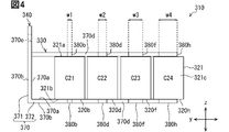
<コンデンサ素子>
図2に示すように平滑コンデンサ310はコンデンサ素子320を8個有している。これら8個のコンデンサ素子320それぞれは同等の製品である。そのために8個のコンデンサ素子320それぞれの静電容量とインダクタンスは同等になっている。ただし、これら8個のコンデンサ素子320の静電容量とインダクタンスには製造誤差などのために±5%程度の差がある。以下においては説明を簡便とするため、8個のコンデンサ素子320に序数を付与して、必要に応じて、第1コンデンサ素子320a~第8コンデンサ素子320hと示す。
<Capacitor element>
As shown in FIG. 2, smoothing
8個のコンデンサ素子320それぞれは、セパレータを介して対向配置する正電極と負電極、および、これらを収納するコンデンサケース321を有する。例えば図2に示すようにコンデンサケース321はz方向を軸方向とする柱形状をなしている。コンデンサケース321はz方向で離間して並ぶ上端面321aと下端面321b、および、これら2つの端面を連結する環状の側面321cを有する。
Each of the eight
図示しないが、上端面321aには上記の正電極と電気的に接続された正端子が設けられている。下端面321bには負電極と電気的に接続された負端子が設けられている。
Although not shown, the
8個のコンデンサ素子320それぞれは、図2に示すようにy方向を行方向、x方向を列方向として行列配置される。本実施形態では8個のコンデンサ素子320が2行4列に配置されている。
Each of the eight
図3と図5に示すように、序数が徐々に増加する態様で4つのコンデンサ素子320が行方向に並んでいる。1行目で序数が奇数の4つのコンデンサ素子320が並んでいる。2行目で序数が偶数の4つのコンデンサ素子320が並んでいる。そして、序数が連番の2つのコンデンサ素子320が列方向で並んでいる。
As shown in FIGS. 3 and 5, the four
詳しく言えば、第1コンデンサ素子320a、第3コンデンサ素子320c、第5コンデンサ素子320e、第7コンデンサ素子320gが1行目で順にy方向に並んでいる。第2コンデンサ素子320b、第4コンデンサ素子320d、第6コンデンサ素子320f、第8コンデンサ素子320hが2行目で順にy方向に並んでいる。
Specifically, the
図面においては、行列配置された8個のコンデンサ素子320に、nを行番号、mを列番号として、記号Cnmを付与している。1行目に位置する序数が奇数の4つのコンデンサ素子320に記号C11,C12,C13,C14を付与している。2行目に位置する序数が偶数の4つのコンデンサ素子320に記号C21,C22,C23,C24を付与している。
In the drawing, eight
図4に示すように8個のコンデンサ素子320の上端面321aそれぞれのz方向の位置は同等になっている。8個の上端面321aは面一になっている。そのために8個のコンデンサ素子320それぞれの正端子のz方向の位置が同等になっている。8個の正端子も2行4列に行列配置されている。これら8個の正端子が正極バスバ330に接続される。
As shown in FIG. 4, the positions of the upper end surfaces 321a of the eight
同様にして、8個のコンデンサ素子320の下端面321bそれぞれのz方向の位置は同等になっている。8個の下端面321bは面一になっている。そのために8個のコンデンサ素子320それぞれの負端子のz方向の位置が同等になっている。8個の負端子も2行4列に行列配置されている。これら8個の負端子が負極バスバ340に接続される。
Similarly, the positions of the lower end surfaces 321b of the eight
<正極バスバと負極バスバ>
正極バスバ330と負極バスバ340は金属製の平板をプレス加工することで製造される。正極バスバ330は8個のコンデンサ素子320それぞれの上端面321a側に設けられる。負極バスバ340は8個のコンデンサ素子320それぞれの下端面321b側に設けられる。正極バスバ330と負極バスバ340がコンデンサ素子用バスバに相当する。
<Positive electrode busbar and negative electrode busbar>
The
正極バスバ330と負極バスバ340それぞれは主バスバ370と枝バスバ380を有する。本実施形態では1個の主バスバ370に8個の枝バスバ380が一体的に連結されている。
Each of the
正極バスバ330の主バスバ370はPバスバ301にボルト止めされる。そして8個の枝バスバ380それぞれは8個の正端子それぞれにはんだや溶接などによって個別に接合される。
The
負極バスバ340の主バスバ370はNバスバ302にボルト止めされる。そして8個の枝バスバ380それぞれは8個の負端子それぞれにはんだや溶接などによって個別に接合される。
The
以上に示した電気的な接続構成により、8個のコンデンサ素子320それぞれは正極バスバ330と負極バスバ340を介してPバスバ301とNバスバ302との間で並列接続されている。8個のコンデンサ素子320それぞれのPバスバ301とNバスバ302との間の通電経路のインピーダンスは正極バスバ330と負極バスバ340それぞれの電気抵抗とインダクタンス、および、コンデンサ素子320のコンダクタンスによって決定されている。
With the electrical connection configuration described above, each of the eight
<主バスバ>
図2~図5に示すように主バスバ370は、延長方向の異なる第1延長部371と第2延長部372を有する。これら延長部の延長方向に直交する断面積は延長方向で一定になっている。そのためにこれら延長部の延長方向におけるインピーダンスは一定になっている。
<Main bus bar>
As shown in FIGS. 2 to 5, the
第1延長部371と第2延長部372とは互いに端部が連結されている。第1延長部371は第2延長部372との連結部位から離間する態様でz方向に延びている。第2延長部372は第1延長部371との連結部位から離間する態様でy方向に延びている。
The ends of the
第1延長部371はy方向の厚さの薄い平板形状をなしている。第2延長部372はz方向の厚さの薄い平板形状をなしている。第1延長部371と第2延長部372それぞれは自身の厚さ方向で並ぶ上面370aと下面370bを有する。第1延長部371と第2延長部372それぞれの上面370aの間の角度が90°になっている。第1延長部371と第2延長部372それぞれの下面370bの間の角度が270°になっている。そのために主バスバ370のx方向に面する平面の形状は、L字形状になっている。なお当然ではあるが、この第1延長部371と第2延長部372との間の角度は適宜変更可能である。
The
第1延長部371における第2延長部372との連結部位から離間した先端側には、上面370aと下面370bとに開口する貫通孔370eが形成されている。この貫通孔370eはPバスバ301若しくはNバスバ302を第1延長部371にボルト止めするためのものである。貫通孔370eが電気回路の接続箇所に相当する。
A through
第1延長部371と第2延長部372それぞれはx方向で並ぶ第1側面370cと第2側面370dを有する。第2延長部372の第1側面370cと第2側面370dそれぞれに枝バスバ380が一体的に連結されている。主バスバ370における枝バスバ380の連結されている場所が連結個所に相当する。
Each of the
<枝バスバ>
図3と図5に示すように、枝バスバ380は第2延長部372の側面から離間する態様でx方向に延びている。第1側面370cに連結された枝バスバ380と第2側面370dに連結された枝バスバ380の延長方向はx方向で逆向きになっている。枝バスバ380における主バスバ370の側面との連結端が一端に相当する。
<Branch bus bar>
As shown in FIGS. 3 and 5, the
第1側面370cと第2側面370dそれぞれに枝バスバ380が4つ連結されている。これら4つの枝バスバ380それぞれの側面での連結位置はy方向で異なっている。第1側面370cに連結された4つの枝バスバ380はy方向で離間して並んでいる。第2側面370dに連結された4つの枝バスバ380はy方向で離間して並んでいる。
Four branch bus bars 380 are connected to each of the
これら計8個の枝バスバ380はy方向を行方向、x方向を列方向として2行4列に行列配置されている。以下においては説明を簡便とするために、8個の枝バスバ380に序数を付与して、必要に応じて、第1枝バスバ380a~第8枝バスバ380hと示す。
These eight
第1側面370cに第1枝バスバ380a、第3枝バスバ380c、第5枝バスバ380e、第7枝バスバ380gが連結されている。これら4つの枝バスバ380に付与した序数は、バスバの通電経路において第2延長部372と第1延長部371との連結部位から離間するほどに増大している。換言すれば、これら4つの枝バスバ380に付与した序数は、バスバの通電経路において第1延長部371の貫通孔370eから離間するほどに増大している。
A first
第2側面370dに第2枝バスバ380b、第4枝バスバ380d、第6枝バスバ380f、第8枝バスバ380hが連結されている。これら4つの枝バスバ380に付与した序数も、バスバの通電経路において第2延長部372と第1延長部371との連結部位から離間するほどに増大している。換言すれば、これら4つの枝バスバ380に付与した序数も、バスバの通電経路において第1延長部371の貫通孔370eから離間するほどに増大している。
A second
第1枝バスバ380aと第2枝バスバ380bはx方向で並んでいる。第3枝バスバ380cと第4枝バスバ380dはx方向で並んでいる。第5枝バスバ380eと第6枝バスバ380fはx方向で並んでいる。第7枝バスバ380gと第8枝バスバ380hはx方向で並んでいる。
The first
本実施形態では、8個の枝バスバ380それぞれのz方向の厚さとx方向(延長方向)の長さは互いに相等しくなっている。そして、x方向で並ぶ2つの枝バスバ380のy方向の長さ(幅)が相等しくなっている。そのため、x方向で並ぶ序数が連番の2つの枝バスバ380の形状は同等になっている。
In this embodiment, the thickness in the z direction and the length in the x direction (extension direction) of each of the eight branch bus bars 380 are equal to each other. The two
しかしながら、y方向で並ぶ4つの枝バスバ380それぞれのy方向の長さ(幅)が異なっている。そのため、y方向で並ぶ序数が奇数の4つの枝バスバ380の形状は相異なっている。y方向で並ぶ序数が偶数の4つの枝バスバ380の形状も相異なっている。
However, the length (width) in the y direction of each of the four
これらy方向で並ぶ4つの枝バスバ380の幅は、図3~図5にw1,w2,w3,w4として示すように、序数が大きくなるにしたがって広くなっている。そのため、序数が大きくなるにしたがって枝バスバ380の延長方向に直交する断面積が増大している。序数が大きくなるにしたがって枝バスバ380の延長方向のインピーダンスが小さくなっている。
The widths of the four
<コンデンサ素子とバスバの連結>
図3と図4に示すように正極バスバ330は、第2延長部372の下面370bがコンデンサ素子320の上端面321aとz方向で対向する態様で8個のコンデンサ素子320に設けられる。この対向配置状態で、正極バスバ330の第1延長部371は8個のコンデンサ素子320のz方向への投影領域外に位置している。
<Connection of Capacitor Element and Bus Bar>
As shown in FIGS. 3 and 4,
正極バスバ330の第1延長部371はコンデンサ素子320の上端面321a側と下端面321b側それぞれから離間する態様でz方向に延びている。第1延長部371のy方向の位置は、2行4列に配置される8個のコンデンサ素子320のうち、1列目に位置する序数が最も小さい2個のコンデンサ素子320と最も近くなっている。
図4と図5に示すように負極バスバ340は、第2延長部372の上面370aがコンデンサ素子320の下端面321bとz方向で対向する態様で8個のコンデンサ素子320に設けられる。この対向配置状態で、負極バスバ340の第1延長部371は8個のコンデンサ素子320のz方向への投影領域外に位置している。
As shown in FIGS. 4 and 5,
負極バスバ340の第1延長部371はz方向において下端面321b側から上端面321a側へと向かって延びている。この第1延長部371のy方向の位置も、2行4列に配置される8個のコンデンサ素子320のうち、1列目に位置する序数が最も小さい2個のコンデンサ素子320と最も近くなっている。
The
正極バスバ330と負極バスバ340それぞれの第1延長部371はx方向で隣り合って並んでいる。正極バスバ330の第1延長部371のx方向の位置は第1行目に位置する序数が奇数の4個のコンデンサ素子320のx方向の位置と同等になっている。負極バスバ340の第1延長部371のx方向の位置は第2行目に位置する序数が偶数の4個のコンデンサ素子320のx方向の位置と同等になっている。正極バスバ330の第1延長部371の第2側面370dと負極バスバ340の第1延長部371の第1側面370cとがx方向で離間しつつ対向している。
The
正極バスバ330の第2延長部372は、上端面321aにおいて1行目の4つの正端子と2行目の4つの正端子との間に設けられる。第2延長部372の第1側面370cから1行目の4つの正端子それぞれに向かって、序数が奇数の4つの枝バスバ380それぞれが個別にx方向に沿って延びている。第2延長部372の第2側面370dから2行目の4つの正端子それぞれに向かって、序数が偶数の4つの枝バスバ380それぞれが個別にx方向に沿って延びている。これら8つの枝バスバ380の先端と8つの正端子とがそれぞれ個別に電気的に接続されている。
The
負極バスバ340の第2延長部372は、下端面321bにおいて1行目の4つの負端子と2行目の4つの負端子との間に設けられる。第2延長部372の第1側面370cから1行目の4つの負端子それぞれに向かって、序数が奇数の4つの枝バスバ380それぞれが個別にx方向に沿って延びている。第2延長部372の第2側面370dから2行目の4つの負端子それぞれに向かって、序数が偶数の4つの枝バスバ380それぞれが個別にx方向に沿って延びている。これら8つの枝バスバ380の先端と8つの負端子とがそれぞれ個別に電気的に接続されている。枝バスバ380の先端が他端に相当する。
The
<インピーダンス>
以上に詳説した平滑コンデンサ310の構成のため、正極バスバ330におけるPバスバ301の接続される貫通孔370eとコンデンサ素子320の正端子との間の通電経路長は、接続対象のコンデンサ素子320の位置する列番号が大きくなるにしたがって長くなっている。負極バスバ340におけるNバスバ302の接続される貫通孔370eとコンデンサ素子320の負端子との間の通電経路長は、接続対象のコンデンサ素子320の位置する列番号が大きくなるにしたがって長くなっている。
<Impedance>
Due to the configuration of the smoothing
8個のコンデンサ素子320に付与した記号で表せば、正極バスバ330と負極バスバ340それぞれの通電経路長は、接続対象のコンデンサ素子320がC11,C12,C13,C14となるにしたがって長くなっている。正極バスバ330と負極バスバ340それぞれの通電経路長は、接続対象のコンデンサ素子320がC21,C22,C23,C24となるにしたがって長くなっている。
In terms of the symbols given to the eight
本実施形態の場合、この正極バスバ330と負極バスバ340の通電経路長の延長は、主バスバ370と枝バスバ380のうち主バスバ370で生じる。主バスバ370における貫通孔370eと枝バスバ380との間の通電経路のインピーダンスが、その枝バスバ380の位置する列番号が大きくなるにしたがって大きくなっている。換言すれば、主バスバ370における貫通孔370eと枝バスバ380との間の通電経路のインピーダンスは、その枝バスバ380の主バスバ370における連結位置が貫通孔370eから遠ざかるほどに大きくなっている。
In the case of this embodiment, the extension of the current path length of the positive
これに対して、1行目と2行目のそれぞれでy方向に並ぶ4つの枝バスバ380の幅は、位置する列番号が大きくなるにしたがって広くなっている。主バスバ370とコンデンサ素子320とを接続する枝バスバ380のインピーダンスは、その枝バスバ380の列番号が大きくなるにしたがって小さくなっている。換言すれば、枝バスバ380のインピーダンスは、その枝バスバ380の主バスバ370における連結位置がバスバの通電経路において貫通孔370eから遠ざかるほどに小さくなっている。
On the other hand, the width of the four
上記の通電経路のインピーダンスを詳説するため、図6と図7に主バスバ370と枝バスバ380それぞれのインピーダンスを記号で表記する。インピーダンスであることを記号Z、正極バスバ330であることを添え字p、負極バスバ340であることを添え字nで示している。また、主バスバ370であることを添え字m、枝バスバ380であることを添え字bで示している。
6 and 7, the impedances of the
正極バスバ330においては、主バスバ370における貫通孔370eと1列目の枝バスバ380との間のインピーダンスをZpm1、1列目の枝バスバ380と2列目の枝バスバ380との間のインピーダンスをZpm2と示す。主バスバ370における2列目の枝バスバ380と3列目の枝バスバ380との間のインピーダンスをZpm3、3列目の枝バスバ380と4列目の枝バスバ380との間のインピーダンスをZpm4と示す。そして、1列目から4列目の枝バスバ380それぞれのインピーダンスを順にZpb1,Zpb2,Zpb3,Zpb4と示す。
In the
負極バスバ340においては、主バスバ370における貫通孔370eと1列目の枝バスバ380との間のインピーダンスをZnm1、1列目の枝バスバ380と2列目の枝バスバ380との間のインピーダンスをZnm2と示す。主バスバ370における2列目の枝バスバ380と3列目の枝バスバ380との間のインピーダンスをZnm3、3列目の枝バスバ380と4列目の枝バスバ380との間のインピーダンスをZnm4と示す。そして、1列目から4列目の枝バスバ380それぞれのインピーダンスを順にZnb1,Znb2,Znb3,Znb4と示す。
In the
これらインピーダンスに基づく平滑コンデンサ310の回路図を図8に示す。1列目から4列目のコンデンサ素子320それぞれの通電経路に対する正極バスバ330と負極バスバ340のインピーダンスの総計をZ1~Z4とすると、これら4つのインピーダンスは以下の数式であらわされる。
A circuit diagram of the smoothing
(数1)
Z1=(Zpm1+Zpb1)+(Znb1+Znm1)
Z2=(Zpm1+Zpm2+Zpb2)+(Znb2+Znm2+Znm1)
Z3=(Zpm1+Zpm2+Zpm3+Zpb3)+(Znb3+Znm3+Znm2+Znm1)
Z4=(Zpm1+Zpm2+Zpm3+Zpm4+Zpb4)+(Znb4+Znm4+Znm3+Znm2+Znm1)
(Number 1)
Z1=(Zpm1+Zpb1)+(Znb1+Znm1)
Z2=(Zpm1+Zpm2+Zpb2)+(Znb2+Znm2+Znm1)
Z3=(Zpm1+Zpm2+Zpm3+Zpb3)+(Znb3+Znm3+Znm2+Znm1)
Z4=(Zpm1+Zpm2+Zpm3+Zpm4+Zpb4)+(Znb4+Znm4+Znm3+Znm2+Znm1)
正極バスバ330と負極バスバ340との区別をなくすと、図8に示す回路図は図9に示す等価回路に変換することができる。この等価回路では、正極バスバ330と負極バスバ340との区別を除去している。図9の等価回路に基づくと、インピーダンスZ1~Z4は以下の数式であらわされる。
If the distinction between the
(数2)
Z1=Zm1+Zb1
Z2=Zm1+Zm2+Zb2
Z3=Zm1+Zm2+Zm3+Zb3
Z4=Zm1+Zm2+Zm3+Zm4+Zb4
(Number 2)
Z1=Zm1+Zb1
Z2 = Zm1 + Zm2 + Zb2
Z3=Zm1+Zm2+Zm3+Zb3
Z4=Zm1+Zm2+Zm3+Zm4+Zb4
また、上記したように枝バスバ380のインピーダンスは、枝バスバ380の列番号が大きくなるにしたがって小さくなっている。そのために1列目から4列目の枝バスバ380のインピーダンスの大小関係は、以下の数式であらわされる。
Also, as described above, the impedance of
(数3)
Zb1<Zb2<Zb3<Zb4
(Number 3)
Zb1<Zb2<Zb3<Zb4
これら数2と数3にあらわされる関係のため、1列目~4列目のコンデンサ素子320それぞれに対する正極バスバ330と負極バスバ340のインピーダンスZ1~Z4の値に差が生じることが抑制されている。
Due to the relationships expressed by these Equations 2 and 3, the occurrence of differences in the values of the impedances Z1 to Z4 of the positive
本実施形態では、Z1=Z2=Z3=Z4が成立するように、8個の枝バスバ380の幅が調整されている。この等式と数2により、以下に示す数式が満たされるように、枝バスバ380の幅が調整されている。
In this embodiment, the widths of the eight
(数4)
Zb1=Zm2+Zb2=Zm2+Zm3+Zb3=Zm2+Zm3+Zm4+Zb4
(Number 4)
Zb1=Zm2+Zb2=Zm2+Zm3+Zb3=Zm2+Zm3+Zm4+Zb4
ただし、製造誤差や接続抵抗などのため、数4で示される関係は厳密には成立しない。インピーダンスZ1~Z4それぞれの値には、少なくとも±5%程度の差がある。 However, strictly speaking, the relationship shown in Equation 4 does not hold due to manufacturing errors, connection resistance, and the like. There is a difference of at least ±5% between the values of the impedances Z1 to Z4.
<作用効果>
上記したように、主バスバ370における貫通孔370eと枝バスバ380との間の通電経路のインピーダンスは、その枝バスバ380の主バスバ370における連結位置が貫通孔370eから遠ざかるほどに大きくなっている。これに反して、枝バスバ380の通電経路のインピーダンスは、その枝バスバ380の主バスバ370における連結位置が貫通孔370eから遠ざかるほどに小さくなっている。そのため、複数のコンデンサ素子320それぞれの正極バスバ330と負極バスバ340における通電経路のインピーダンスに差が生じることが抑制される。
<Effect>
As described above, the impedance of the current path between the through
また、複数のコンデンサ素子320それぞれのコンダクタンスは同等になっている。そのため、複数のコンデンサ素子320それぞれのPバスバ301とNバスバ302との間の通電経路のインピーダンスに差が生じることが抑制される。図8と図9に示す1列目~4列目のコンデンサ素子320それぞれに流れる電流I1~I4の量に差が生じることが抑制されている。
Also, the conductance of each of the plurality of
この結果、複数のコンデンサ素子320それぞれに発生するジュール熱に差が生じることが抑制される。複数のコンデンサ素子320それぞれの寿命に差が生じることが抑制される。
As a result, the occurrence of differences in Joule heat generated in each of the plurality of
また、複数のコンデンサ素子320それぞれに発生するクーロン力が一部で極端に高くなることが抑制される。スイッチ群350に含まれるスイッチのPWM制御のために、電流の時間変化によるクーロン力の作用方向の変化によって複数のコンデンサ素子320が振動する振る舞いを示したとしても、その振動振幅が一部で極端に増大することが抑制される。コンデンサ素子320の振動による異音の発生が抑制される。
Also, the Coulomb force generated in each of the plurality of
(第2実施形態)
次に、第2実施形態を図10および図11に基づいて説明する。
(Second embodiment)
Next, a second embodiment will be described with reference to FIGS. 10 and 11. FIG.
第1実施形態では、y方向に並ぶ4つの枝バスバ380の幅が異なる例を示した。これに対して本実施形態ではy方向に並ぶ4つの枝バスバ380の厚さが異なっている。
In the first embodiment, an example in which the four
これらy方向で並ぶ4つの枝バスバ380の厚さは、図11にt1,t2,t3,t4として示すように、序数が大きくなるにしたがって厚くなっている。そのため、序数が大きくなるにしたがって枝バスバ380の延長方向に直交する断面積が増大している。枝バスバ380の通電経路のインピーダンスは、その枝バスバ380の主バスバ370における連結位置が貫通孔370eから遠ざかるほどに小さくなっている。
The thickness of the four
このように本実施形態に係る電力変換装置300には第1実施形態に記載の電力変換装置300と同様の構成要素が含まれている。そのために本実施形態に係る電力変換装置300も第1実施形態に記載の電力変換装置300と同等の作用効果を奏することは言うまでもない。以下に示す他の実施形態においても作用効果については同等である。そのためにその記載を省略する。
As described above, the
(第3実施形態)
次に、第3実施形態を図12および図13に基づいて説明する。
(Third Embodiment)
Next, a third embodiment will be described with reference to FIGS. 12 and 13. FIG.
第1実施形態では、y方向に並ぶ4つの枝バスバ380の幅が、その枝バスバ380の主バスバ370における連結位置が貫通孔370eから遠ざかるほどに広くなっている例を示した。これに対して本実施形態ではy方向に並ぶ4つの枝バスバ380それぞれの形状は同等になっている。しかしながら図12と図13において白丸の数の相違で示すように、4つの枝バスバ380それぞれのコンデンサ素子320との接続面積が、その枝バスバ380の主バスバ370における連結位置が貫通孔370eから遠ざかるほどに広くなっている。
In the first embodiment, the width of the four
そのため、枝バスバ380とコンデンサ素子320との間のインピーダンスは、枝バスバ380の主バスバ370における連結位置が貫通孔370eから遠ざかるほどに小さくなっている。なお、上記の接続面積の大小関係は、半田接続であれば、半田の塗布量や塗布面積の調整などによって実現される。接続面積の大小関係は、レーザ溶接であれば、溶接点の数の調整などによって実現される。
Therefore, the impedance between
(第4実施形態)
次に、第4実施形態を図14に基づいて説明する。
(Fourth embodiment)
Next, a fourth embodiment will be described with reference to FIG.
第1実施形態ではy方向に並ぶ4つの枝バスバ380の幅が異なる例を示した。これに対して本実施形態ではy方向に並ぶ4つの枝バスバ380の延長方向(x方向)の長さが異なっている。
In the first embodiment, the four
これらy方向で並ぶ4つの枝バスバ380の長さは、図14にl1,l2,l3,l4として示すように、序数が大きくなるにしたがって短くなっている。そのため、枝バスバ380の通電経路のインピーダンスは、その枝バスバ380の主バスバ370における連結位置が貫通孔370eから遠ざかるほどに小さくなっている。
The lengths of the four
(第5実施形態)
次に、第5実施形態を図15に基づいて説明する。
(Fifth embodiment)
Next, a fifth embodiment will be described with reference to FIG.
第1実施形態ではy方向に並ぶ4つの枝バスバ380の幅が異なる例を示した。これに対して本実施形態ではy方向に並ぶ4つの枝バスバ380それぞれに切り欠き381が形成されている。
In the first embodiment, the four
これらy方向で並ぶ4つの枝バスバ380に形成される切り欠き381の大きさは、序数が大きくなるにしたがって小さくなっている。そのため、枝バスバ380の通電経路のインピーダンスは、その枝バスバ380の主バスバ370における連結位置が貫通孔370eに近いほどに大きくなっている。
The size of the
なお、図15においてはy方向に並ぶ4つの枝バスバ380のうちの序数が最も大きい枝バスバ380に切り欠き381が形成されていない例を示した。しかしながら、4つの枝バスバ380のすべてに切り欠き381が形成された構成を採用することもできる。
Note that FIG. 15 shows an example in which the
また、図15においては枝バスバ380に孔形状の切り欠き381が形成された例を示した。しかしながらこの形態に限らず、枝バスバ380の厚さ、幅、長さの少なくとも1つが局所的に切り欠くことで、枝バスバ380に切り欠き381の形成された構成を採用することもできる。
Also, FIG. 15 shows an example in which a hole-shaped
(第6実施形態)
次に、第6実施形態を図16に基づいて説明する。
(Sixth embodiment)
Next, a sixth embodiment will be described with reference to FIG.
これまでに例示した実施形態では8つの枝バスバ380それぞれが主バスバ370に一体的に連結された例を示した。これに対して本実施形態では8つの枝バスバ380の一部が主バスバ370に溶接などによって接合された構成になっている。8つの枝バスバ380の一部が導電性の異種材料(金属)で構成されている。
In the embodiments illustrated so far, eight
1列目に位置する2つの枝バスバ380それぞれは主バスバ370と同一の金属材料で構成されている。しかしながら2列目に位置する2つの枝バスバ380と3列目に位置する枝バスバ380それぞれは、主バスバ370と同一の金属材料と、他の異種材料とによって構成されている。4列目に位置する2つの枝バスバ380は異種材料で構成されている。図面においては異種材料にハッチングを付与するとともに、この異種材料と主バスバ370と同一の金属材料との接合部位に破線を付与している。以下においては表記を簡明とするために主バスバ370と同一の金属材料を同種材料と示す。
Each of the two
これら1列目から4列目の枝バスバ380それぞれの形状は同一である。異種材料は同種材料よりも低効率若しくは透磁率が低くなっている。そのために異種材料は同種材料よりも低インピーダンスになっている。そして、2列目の枝バスバ380に含まれる異種材料よりも3列目の枝バスバ380に含まれる異種材料が多くなっている。
The shape of each of the
係る構成のため、枝バスバ380の通電経路のインピーダンスは、その枝バスバ380の位置する列番号が大きくなるにしたがって小さくなっている。換言すれば、枝バスバ380のインピーダンスは、その枝バスバ380の主バスバ370における連結位置が貫通孔370eから遠いほどに小さくなっている。
Due to this configuration, the impedance of the energization path of the
なお、本実施形態では枝バスバ380の構成材料として、同種材料と、1種類の異種材料と、が採用される例を示した。しかしながら枝バスバ380の構成材料としてはこれら2種類に限定されない。例えば図17においてハッチングを異ならせて示すように、1列目から4列目それぞれの枝バスバ380の構成材料を異ならせてもよい。図17に示す変形例の場合、枝バスバ380の構成材料のインピーダンスは、その枝バスバ380の位置する列番号が大きくなるにしたがって小さくなっている。
In addition, in this embodiment, as the constituent material of the
本実施形態では複数の枝バスバ380の一部が主バスバ370に一体的に連結される例を示した。しかしながら例えば図17に示すようにすべての枝バスバ380が主バスバ370と別体であり、その別体の枝バスバ380が主バスバ370に溶接などによって接合される構成を採用することもできる。係る変形例の場合、主バスバ370の形状を簡素化することができる。
In this embodiment, an example in which some of the plurality of
(第1の変形例)
各実施形態ではy方向で並ぶ4つの枝バスバ380それぞれがy方向で離間する例を示した。しかしながら例えば図18に示すようにy方向で並ぶ4つの枝バスバ380の一部が互いに連結された構成を採用することもできる。
(First modification)
Each embodiment shows an example in which the four
図18に示す変形例では、2列目の枝バスバ380に破線で示す第1追加部分382が追加されている。3列目の枝バスバ380に一点鎖線で示す第2追加部分383が追加されている。4列目の枝バスバ380に二点鎖線で示す第3追加部分384が追加されている。
In the modification shown in FIG. 18, a first
第1追加部分382は第2追加部分383よりも幅と長さとが短くなっている。第1追加部分382と第2追加部分383とが連結されている。
The first
第2追加部分383は第3追加部分384よりも幅と長さとが短くなっている。第2追加部分383と第3追加部分384とが連結されている。
The second
(第2の変形例)
各実施形態では平滑コンデンサ310が8個のコンデンサ素子320を有する例を示した。しかしながら平滑コンデンサ310が備えるコンデンサ素子320の数としては複数であればよく上記例に限定されない。
(Second modification)
Each embodiment has shown an example in which the smoothing
例えば図19に示すように平滑コンデンサ310は4個のコンデンサ素子320を有してもよい。これら4個のコンデンサ素子320は1行4列に配置されている。正極バスバ330と負極バスバ340それぞれは4つの枝バスバ380を備えている。
For example, the smoothing
図示しないが、他の複数のコンデンサ素子320の行列配置においても、これまでに提示した実施形態と変形例に記載の枝バスバ380の構成を適宜組み合わせることで、第1実施形態に記載の作用効果と同等の作用効果を奏することができる。
Although not shown, in other matrix arrangements of a plurality of
(その他の変形例)
本実施形態では電力変換装置300が電気自動車用の車載システムに適用される例を示した。しかしながら電力変換装置300、これに含まれる平滑コンデンサ310、および、これに含まれる正極バスバ330と負極バスバ340それぞれは、他の例えばハイブリッド自動車用の車載システムに適用することもできる。
(Other modifications)
In this embodiment, an example in which the
本実施形態では電力変換装置300がインバータを含む例を示した。しかしながら電力変換装置300はコンバータを含んでもよい。そして本実施形態に記載の平滑コンデンサ310に適用された各種構成を、コンバータに含まれるフィルタコンデンサに適用してもよい。
In this embodiment, the example in which the
さらに言えば、本開示に記載の平滑コンデンサ310に適用された各種構成は、電力変換回路に含まれるコンデンサだけではなく、電力変換回路に電気的に接続される電気回路に含まれるコンデンサに適用することもできる。平滑コンデンサ310に適用された各種構成は、第1実施形態に記載した、複数のコンデンサ素子320の電流量の差に起因するジュール熱差などの課題のあるコンデンサ、および、それを含む電気回路に適用可能である。
Furthermore, the various configurations applied to smoothing
本実施形態では正極バスバ330がPバスバ301にボルト止めされ、負極バスバ340がNバスバ302にボルト止めされる例を示した。しかしながら正極バスバ330とPバスバ301とは別体ではなく一体でもよい。負極バスバ340とNバスバ302とは別体ではなく一体でもよい。複数のコンデンサ素子320それぞれにPバスバ301とNバスバ302がはんだなどによって接続された構成を採用することもできる。
In this embodiment, an example in which the
この変形例においては、複数のコンデンサ素子320それぞれのスイッチ群350に含まれるハイサイドスイッチ361とローサイドスイッチ362との間の通電経路のインピーダンスに差が生じることが抑制される。
In this modification, occurrence of a difference in impedance between the high-
本開示では、複数の枝バスバ380のインピーダンスに差を設けるための構成例を実施形態と変形例で種々説明した。延長方向に直交する断面積の大きさ、コンデンサ素子320との接続面積の大きさ、延長方向の長さ、切り欠き381の有無と大きさ、異種材料の有無と物性と大きさなどに差を設けることで複数の枝バスバ380のインピーダンスに差を設ける例などを説明した。これらのうちの少なくとも2つを選択することで、複数の枝バスバ380のインピーダンスに差を設けてもよい。
In the present disclosure, various configuration examples for providing differences in the impedances of the plurality of branch bus bars 380 have been described in the embodiments and modifications. The size of the cross-sectional area orthogonal to the extension direction, the size of the connection area with the
本開示は、実施例に準拠して記述されたが、本開示は当該実施例や構造に限定されるものではないと理解される。本開示は、様々な変形例や均等範囲内の変形をも包含する。加えて、様々な組み合わせや形態が本開示に示されているが、それらに一要素のみ、それ以上、あるいはそれ以下、を含む他の組み合わせや形態をも、本開示の範疇や思想範囲に入るものである。 Although the present disclosure has been described with reference to examples, it is understood that the present disclosure is not limited to such examples or structures. The present disclosure also includes various modifications and modifications within the equivalent range. In addition, while various combinations and configurations are shown in this disclosure, other combinations and configurations, including single elements, more, or less, are within the scope and spirit of this disclosure. It is.
100…車載システム、200…バッテリ、300…電力変換装置、301…Pバスバ、302…Nバスバ、310…平滑コンデンサ、320…コンデンサ素子、320a~320h…第1コンデンサ素子~第8コンデンサ素子、330…正極バスバ、340…負極バスバ、350…スイッチ群、361…ハイサイドスイッチ、362…ローサイドスイッチ、370…主バスバ、370e…貫通孔、380…枝バスバ、380a~380h…第1枝バスバ~第8枝バスバ、381…切り欠き、400…モータ
DESCRIPTION OF
Claims (8)
前記正極バスバおよび前記負極バスバそれぞれは、下面(370b)または上面(370a)が上端面(321a)または下端面(321b)に対向する態様で設けられるとともに前記電気回路に電気的に接続される主バスバ(370)と、それぞれ前記主バスバの異なる場所に一端が連結され、複数の前記コンデンサ素子それぞれの前記正電極または前記負電極に他端が個別に連結される複数の枝バスバ(380a~380h)と、を有し、
複数の前記枝バスバそれぞれの前記一端と前記コンデンサ素子に接続される前記他端との間のインピーダンスは、前記主バスバにおける前記電気回路の接続箇所(370e)と前記一端の連結個所との間のインピーダンスが大きくなるほどに、小さくなっているコンデンサ素子用バスバ。 Each of a plurality of capacitor elements (320a to 320h) having the same inductance and having positive and negative electrodes on the end faces (321a, 321b) is electrically connected to an electric circuit (350) including switch elements (361, 362). having a positive electrode bus bar (301, 330) and a negative electrode bus bar (302, 340),
Each of the positive electrode bus bar and the negative electrode bus bar is provided in such a manner that the lower surface (370b) or the upper surface (370a) faces the upper end surface (321a) or the lower end surface (321b) and is electrically connected to the electric circuit. a bus bar (370), and a plurality of branch bus bars (380a to 380h) each having one end connected to a different location of the main bus bar and having the other end individually connected to the positive electrode or the negative electrode of each of the plurality of capacitor elements. ), and
The impedance between the one end of each of the plurality of branch bus bars and the other end connected to the capacitor element is the impedance between the electrical circuit connection point (370e) of the main bus bar and the connection point of the one end. A busbar for a capacitor element that becomes smaller as the impedance increases.
複数の前記コンデンサ素子それぞれとスイッチ素子(361,362)を含む電気回路(350)とを電気的に接続する正極バスバ(301,330)および負極バスバ(302,340)と、を有し、
前記正極バスバおよび前記負極バスバそれぞれは、下面(370b)または上面(370a)が上端面(321a)または下端面(321b)に対向する態様で設けられるとともに前記電気回路に電気的に接続される主バスバ(370)と、それぞれ前記主バスバの異なる場所に一端が連結され、複数の前記コンデンサ素子それぞれの前記正電極または前記負電極に他端が個別に連結される複数の枝バスバ(380a~380h)と、を有し、
複数の前記枝バスバそれぞれの前記一端と前記コンデンサ素子に接続される前記他端との間のインピーダンスは、前記主バスバにおける前記電気回路の接続箇所(370e)と前記一端の連結個所との間のインピーダンスが大きくなるほどに、小さくなっているコンデンサ。 a plurality of capacitor elements (320a to 320h) having the same inductance and having positive and negative electrodes on the end faces (321a, 321b) ;
positive bus bars (301, 330) and negative bus bars (302, 340) electrically connecting each of the plurality of capacitor elements and an electric circuit (350) including switch elements (361, 362);
Each of the positive electrode bus bar and the negative electrode bus bar is provided in such a manner that the lower surface (370b) or the upper surface (370a) faces the upper end surface (321a) or the lower end surface (321b) and is electrically connected to the electric circuit. a bus bar (370), and a plurality of branch bus bars (380a to 380h) each having one end connected to a different location of the main bus bar and having the other end individually connected to the positive electrode or the negative electrode of each of the plurality of capacitor elements. ), and
The impedance between the one end of each of the plurality of branch bus bars and the other end connected to the capacitor element is the impedance between the electrical circuit connection point (370e) of the main bus bar and the connection point of the one end. A capacitor that becomes smaller as the impedance increases.
端面(321a,321b)に正電極および負電極を備えるインダクタンスの同等な複数のコンデンサ素子(320a~320h)と、
複数の前記コンデンサ素子それぞれと前記電気回路とを電気的に接続する正極バスバ(301,330)および負極バスバ(302,340)と、を有し、
前記正極バスバおよび前記負極バスバそれぞれは、下面(370b)または上面(370a)が上端面(321a)または下端面(321b)に対向する態様で設けられるとともに前記電気回路に電気的に接続される主バスバ(370)と、それぞれ前記主バスバの異なる場所に一端が連結され、複数の前記コンデンサ素子それぞれの前記正電極または前記負電極に他端が個別に連結される複数の枝バスバ(380a~380h)と、を有し、
複数の前記枝バスバそれぞれの前記一端と前記コンデンサ素子に接続される前記他端との間のインピーダンスは、前記主バスバにおける前記電気回路の接続箇所(370e)と前記一端の連結個所との間のインピーダンスが大きくなるほどに、小さくなっている電力変換装置。 an electrical circuit (350) including switch elements (361, 362);
a plurality of capacitor elements (320a to 320h) having the same inductance and having positive and negative electrodes on the end faces (321a, 321b) ;
a positive bus bar (301, 330) and a negative bus bar (302, 340) electrically connecting each of the plurality of capacitor elements and the electric circuit;
Each of the positive electrode bus bar and the negative electrode bus bar is provided in such a manner that the lower surface (370b) or the upper surface (370a) faces the upper end surface (321a) or the lower end surface (321b) and is electrically connected to the electric circuit. a bus bar (370), and a plurality of branch bus bars (380a to 380h) each having one end connected to a different location of the main bus bar and having the other end individually connected to the positive electrode or the negative electrode of each of the plurality of capacitor elements. ), and
The impedance between the one end of each of the plurality of branch bus bars and the other end connected to the capacitor element is the impedance between the electrical circuit connection point (370e) of the main bus bar and the connection point of the one end. A power conversion device that becomes smaller as the impedance increases.
Priority Applications (3)
| Application Number | Priority Date | Filing Date | Title |
|---|---|---|---|
| JP2020060724A JP7167959B2 (en) | 2020-03-30 | 2020-03-30 | BUS BAR FOR CAPACITOR ELEMENTS, CAPACITORS AND POWER CONVERTERS |
| PCT/JP2021/004104 WO2021199670A1 (en) | 2020-03-30 | 2021-02-04 | Busbar for capacitor element, capacitor, and power conversion device |
| US17/954,850 US20230021288A1 (en) | 2020-03-30 | 2022-09-28 | Bus bar for capacitor elements, capacitor, and power conversion device |
Applications Claiming Priority (1)
| Application Number | Priority Date | Filing Date | Title |
|---|---|---|---|
| JP2020060724A JP7167959B2 (en) | 2020-03-30 | 2020-03-30 | BUS BAR FOR CAPACITOR ELEMENTS, CAPACITORS AND POWER CONVERTERS |
Publications (3)
| Publication Number | Publication Date |
|---|---|
| JP2021164169A JP2021164169A (en) | 2021-10-11 |
| JP2021164169A5 JP2021164169A5 (en) | 2022-01-31 |
| JP7167959B2 true JP7167959B2 (en) | 2022-11-09 |
Family
ID=77927730
Family Applications (1)
| Application Number | Title | Priority Date | Filing Date |
|---|---|---|---|
| JP2020060724A Active JP7167959B2 (en) | 2020-03-30 | 2020-03-30 | BUS BAR FOR CAPACITOR ELEMENTS, CAPACITORS AND POWER CONVERTERS |
Country Status (3)
| Country | Link |
|---|---|
| US (1) | US20230021288A1 (en) |
| JP (1) | JP7167959B2 (en) |
| WO (1) | WO2021199670A1 (en) |
Families Citing this family (4)
| Publication number | Priority date | Publication date | Assignee | Title |
|---|---|---|---|---|
| JP7156319B2 (en) * | 2020-01-22 | 2022-10-19 | 株式会社デンソー | power converter |
| USD1026830S1 (en) * | 2021-07-19 | 2024-05-14 | Delta Electronics (Shanghai) Co., Ltd. | Electrical bus bar |
| JP2023067149A (en) * | 2021-10-29 | 2023-05-16 | マツダ株式会社 | Inverter structure |
| DE102022123261B4 (en) | 2022-09-13 | 2024-09-26 | Semikron Elektronik Gmbh & Co. Kg | Power electronic assembly with a housing and with a capacitor device arranged therein |
Citations (5)
| Publication number | Priority date | Publication date | Assignee | Title |
|---|---|---|---|---|
| JP2008251594A (en) | 2007-03-29 | 2008-10-16 | Matsushita Electric Ind Co Ltd | Case-mold capacitor |
| JP2009099884A (en) | 2007-10-19 | 2009-05-07 | Toyota Motor Corp | Capacitor |
| JP2011035027A (en) | 2009-07-30 | 2011-02-17 | Toyota Motor Corp | Capacitor assembly |
| JP2011096917A (en) | 2009-10-30 | 2011-05-12 | Denso Corp | Capacitor and power converter |
| JP2011124434A (en) | 2009-12-11 | 2011-06-23 | Denso Corp | Capacitor module |
Family Cites Families (6)
| Publication number | Priority date | Publication date | Assignee | Title |
|---|---|---|---|---|
| JPH09320891A (en) * | 1996-05-27 | 1997-12-12 | Nissin Electric Co Ltd | Capacitor device |
| JPH10146064A (en) * | 1996-11-07 | 1998-05-29 | Fuji Electric Co Ltd | Structure of cubicle for power converter |
| JP5796257B2 (en) * | 2012-05-31 | 2015-10-21 | アイシン・エィ・ダブリュ株式会社 | Inverter device |
| JP2014203893A (en) * | 2013-04-02 | 2014-10-27 | トヨタ自動車株式会社 | Capacitor module |
| US11088649B2 (en) * | 2017-04-27 | 2021-08-10 | Mitsubishi Electric Corporation | Power conversion unit |
| US10483048B2 (en) * | 2017-05-15 | 2019-11-19 | Honda Motor Co., Ltd. | Capacitor-type power supply unit |
-
2020
- 2020-03-30 JP JP2020060724A patent/JP7167959B2/en active Active
-
2021
- 2021-02-04 WO PCT/JP2021/004104 patent/WO2021199670A1/en active Application Filing
-
2022
- 2022-09-28 US US17/954,850 patent/US20230021288A1/en active Pending
Patent Citations (5)
| Publication number | Priority date | Publication date | Assignee | Title |
|---|---|---|---|---|
| JP2008251594A (en) | 2007-03-29 | 2008-10-16 | Matsushita Electric Ind Co Ltd | Case-mold capacitor |
| JP2009099884A (en) | 2007-10-19 | 2009-05-07 | Toyota Motor Corp | Capacitor |
| JP2011035027A (en) | 2009-07-30 | 2011-02-17 | Toyota Motor Corp | Capacitor assembly |
| JP2011096917A (en) | 2009-10-30 | 2011-05-12 | Denso Corp | Capacitor and power converter |
| JP2011124434A (en) | 2009-12-11 | 2011-06-23 | Denso Corp | Capacitor module |
Also Published As
| Publication number | Publication date |
|---|---|
| JP2021164169A (en) | 2021-10-11 |
| US20230021288A1 (en) | 2023-01-19 |
| WO2021199670A1 (en) | 2021-10-07 |
Similar Documents
| Publication | Publication Date | Title |
|---|---|---|
| JP7167959B2 (en) | BUS BAR FOR CAPACITOR ELEMENTS, CAPACITORS AND POWER CONVERTERS | |
| EP2568787B1 (en) | Semiconductor device and power conversion apparatus using the same | |
| US20060273592A1 (en) | Power unit | |
| CN110720173A (en) | Modular intermediate circuit for an inverter, inverter circuit, energy converter and vehicle | |
| JP3709512B2 (en) | Main circuit structure of power converter | |
| US11394311B2 (en) | Power conversion apparatus | |
| US20190123622A1 (en) | Power conversion device | |
| WO2022163226A1 (en) | Electrical appliance | |
| CN110323952B (en) | Power conversion device | |
| US11973432B2 (en) | Power conversion apparatus | |
| WO2022054476A1 (en) | Power conversion device | |
| WO2021256175A1 (en) | Power conversion device | |
| JP7294247B2 (en) | electric unit | |
| WO2021039237A1 (en) | Current-carrying part for power conversion circuit | |
| WO2022176447A1 (en) | Electric device | |
| JP2020162226A (en) | Power conversion unit | |
| JP7099300B2 (en) | Power conversion unit | |
| JP7205516B2 (en) | power converter | |
| JP7322835B2 (en) | power converter | |
| CN111404397B (en) | power conversion device | |
| CN112019066B (en) | power conversion unit | |
| JP2019180114A (en) | Power conversion device and capacitor for power conversion device | |
| US11973433B2 (en) | Power conversion apparatus | |
| JP7110772B2 (en) | power converter | |
| JP2021180541A (en) | Power conversion device |
Legal Events
| Date | Code | Title | Description |
|---|---|---|---|
| A521 | Request for written amendment filed |
Free format text: JAPANESE INTERMEDIATE CODE: A523 Effective date: 20220121 |
|
| A621 | Written request for application examination |
Free format text: JAPANESE INTERMEDIATE CODE: A621 Effective date: 20220121 |
|
| TRDD | Decision of grant or rejection written | ||
| A01 | Written decision to grant a patent or to grant a registration (utility model) |
Free format text: JAPANESE INTERMEDIATE CODE: A01 Effective date: 20220927 |
|
| A61 | First payment of annual fees (during grant procedure) |
Free format text: JAPANESE INTERMEDIATE CODE: A61 Effective date: 20221010 |
|
| R151 | Written notification of patent or utility model registration |
Ref document number: 7167959 Country of ref document: JP Free format text: JAPANESE INTERMEDIATE CODE: R151 |