JP7166324B2 - Indium phosphide substrate, method for producing indium phosphide substrate, and semiconductor epitaxial wafer - Google Patents
Indium phosphide substrate, method for producing indium phosphide substrate, and semiconductor epitaxial wafer Download PDFInfo
- Publication number
- JP7166324B2 JP7166324B2 JP2020211685A JP2020211685A JP7166324B2 JP 7166324 B2 JP7166324 B2 JP 7166324B2 JP 2020211685 A JP2020211685 A JP 2020211685A JP 2020211685 A JP2020211685 A JP 2020211685A JP 7166324 B2 JP7166324 B2 JP 7166324B2
- Authority
- JP
- Japan
- Prior art keywords
- indium phosphide
- wafer
- substrate
- phosphide substrate
- edge portion
- Prior art date
- Legal status (The legal status is an assumption and is not a legal conclusion. Google has not performed a legal analysis and makes no representation as to the accuracy of the status listed.)
- Active
Links
Images
Classifications
-
- C—CHEMISTRY; METALLURGY
- C30—CRYSTAL GROWTH
- C30B—SINGLE-CRYSTAL GROWTH; UNIDIRECTIONAL SOLIDIFICATION OF EUTECTIC MATERIAL OR UNIDIRECTIONAL DEMIXING OF EUTECTOID MATERIAL; REFINING BY ZONE-MELTING OF MATERIAL; PRODUCTION OF A HOMOGENEOUS POLYCRYSTALLINE MATERIAL WITH DEFINED STRUCTURE; SINGLE CRYSTALS OR HOMOGENEOUS POLYCRYSTALLINE MATERIAL WITH DEFINED STRUCTURE; AFTER-TREATMENT OF SINGLE CRYSTALS OR A HOMOGENEOUS POLYCRYSTALLINE MATERIAL WITH DEFINED STRUCTURE; APPARATUS THEREFOR
- C30B29/00—Single crystals or homogeneous polycrystalline material with defined structure characterised by the material or by their shape
- C30B29/10—Inorganic compounds or compositions
- C30B29/40—AIIIBV compounds wherein A is B, Al, Ga, In or Tl and B is N, P, As, Sb or Bi
-
- C—CHEMISTRY; METALLURGY
- C30—CRYSTAL GROWTH
- C30B—SINGLE-CRYSTAL GROWTH; UNIDIRECTIONAL SOLIDIFICATION OF EUTECTIC MATERIAL OR UNIDIRECTIONAL DEMIXING OF EUTECTOID MATERIAL; REFINING BY ZONE-MELTING OF MATERIAL; PRODUCTION OF A HOMOGENEOUS POLYCRYSTALLINE MATERIAL WITH DEFINED STRUCTURE; SINGLE CRYSTALS OR HOMOGENEOUS POLYCRYSTALLINE MATERIAL WITH DEFINED STRUCTURE; AFTER-TREATMENT OF SINGLE CRYSTALS OR A HOMOGENEOUS POLYCRYSTALLINE MATERIAL WITH DEFINED STRUCTURE; APPARATUS THEREFOR
- C30B25/00—Single-crystal growth by chemical reaction of reactive gases, e.g. chemical vapour-deposition growth
- C30B25/02—Epitaxial-layer growth
- C30B25/18—Epitaxial-layer growth characterised by the substrate
- C30B25/186—Epitaxial-layer growth characterised by the substrate being specially pre-treated by, e.g. chemical or physical means
-
- C—CHEMISTRY; METALLURGY
- C30—CRYSTAL GROWTH
- C30B—SINGLE-CRYSTAL GROWTH; UNIDIRECTIONAL SOLIDIFICATION OF EUTECTIC MATERIAL OR UNIDIRECTIONAL DEMIXING OF EUTECTOID MATERIAL; REFINING BY ZONE-MELTING OF MATERIAL; PRODUCTION OF A HOMOGENEOUS POLYCRYSTALLINE MATERIAL WITH DEFINED STRUCTURE; SINGLE CRYSTALS OR HOMOGENEOUS POLYCRYSTALLINE MATERIAL WITH DEFINED STRUCTURE; AFTER-TREATMENT OF SINGLE CRYSTALS OR A HOMOGENEOUS POLYCRYSTALLINE MATERIAL WITH DEFINED STRUCTURE; APPARATUS THEREFOR
- C30B33/00—After-treatment of single crystals or homogeneous polycrystalline material with defined structure
-
- H—ELECTRICITY
- H10—SEMICONDUCTOR DEVICES; ELECTRIC SOLID-STATE DEVICES NOT OTHERWISE PROVIDED FOR
- H10D—INORGANIC ELECTRIC SEMICONDUCTOR DEVICES
- H10D62/00—Semiconductor bodies, or regions thereof, of devices having potential barriers
- H10D62/80—Semiconductor bodies, or regions thereof, of devices having potential barriers characterised by the materials
- H10D62/85—Semiconductor bodies, or regions thereof, of devices having potential barriers characterised by the materials being Group III-V materials, e.g. GaAs
-
- H—ELECTRICITY
- H10—SEMICONDUCTOR DEVICES; ELECTRIC SOLID-STATE DEVICES NOT OTHERWISE PROVIDED FOR
- H10P—GENERIC PROCESSES OR APPARATUS FOR THE MANUFACTURE OR TREATMENT OF DEVICES COVERED BY CLASS H10
- H10P14/00—Formation of materials, e.g. in the shape of layers or pillars
- H10P14/20—Formation of materials, e.g. in the shape of layers or pillars of semiconductor materials
- H10P14/29—Formation of materials, e.g. in the shape of layers or pillars of semiconductor materials characterised by the substrates
- H10P14/2901—Materials
- H10P14/2907—Materials being Group IIIA-VA materials
- H10P14/2909—Phosphides
-
- H—ELECTRICITY
- H10—SEMICONDUCTOR DEVICES; ELECTRIC SOLID-STATE DEVICES NOT OTHERWISE PROVIDED FOR
- H10P—GENERIC PROCESSES OR APPARATUS FOR THE MANUFACTURE OR TREATMENT OF DEVICES COVERED BY CLASS H10
- H10P52/00—Grinding, lapping or polishing of wafers, substrates or parts of devices
-
- H—ELECTRICITY
- H10—SEMICONDUCTOR DEVICES; ELECTRIC SOLID-STATE DEVICES NOT OTHERWISE PROVIDED FOR
- H10P—GENERIC PROCESSES OR APPARATUS FOR THE MANUFACTURE OR TREATMENT OF DEVICES COVERED BY CLASS H10
- H10P90/00—Preparation of wafers not covered by a single main group of this subclass, e.g. wafer reinforcement
- H10P90/12—Preparing bulk and homogeneous wafers
- H10P90/126—Preparing bulk and homogeneous wafers by chemical etching
-
- H—ELECTRICITY
- H10—SEMICONDUCTOR DEVICES; ELECTRIC SOLID-STATE DEVICES NOT OTHERWISE PROVIDED FOR
- H10P—GENERIC PROCESSES OR APPARATUS FOR THE MANUFACTURE OR TREATMENT OF DEVICES COVERED BY CLASS H10
- H10P90/00—Preparation of wafers not covered by a single main group of this subclass, e.g. wafer reinforcement
- H10P90/12—Preparing bulk and homogeneous wafers
- H10P90/128—Preparing bulk and homogeneous wafers by edge treatment, e.g. chamfering
-
- H—ELECTRICITY
- H10—SEMICONDUCTOR DEVICES; ELECTRIC SOLID-STATE DEVICES NOT OTHERWISE PROVIDED FOR
- H10P—GENERIC PROCESSES OR APPARATUS FOR THE MANUFACTURE OR TREATMENT OF DEVICES COVERED BY CLASS H10
- H10P90/00—Preparation of wafers not covered by a single main group of this subclass, e.g. wafer reinforcement
- H10P90/12—Preparing bulk and homogeneous wafers
- H10P90/129—Preparing bulk and homogeneous wafers by polishing
-
- H—ELECTRICITY
- H10—SEMICONDUCTOR DEVICES; ELECTRIC SOLID-STATE DEVICES NOT OTHERWISE PROVIDED FOR
- H10P—GENERIC PROCESSES OR APPARATUS FOR THE MANUFACTURE OR TREATMENT OF DEVICES COVERED BY CLASS H10
- H10P14/00—Formation of materials, e.g. in the shape of layers or pillars
- H10P14/20—Formation of materials, e.g. in the shape of layers or pillars of semiconductor materials
- H10P14/29—Formation of materials, e.g. in the shape of layers or pillars of semiconductor materials characterised by the substrates
- H10P14/2924—Structures
- H10P14/2925—Surface structures
-
- H—ELECTRICITY
- H10—SEMICONDUCTOR DEVICES; ELECTRIC SOLID-STATE DEVICES NOT OTHERWISE PROVIDED FOR
- H10P—GENERIC PROCESSES OR APPARATUS FOR THE MANUFACTURE OR TREATMENT OF DEVICES COVERED BY CLASS H10
- H10P14/00—Formation of materials, e.g. in the shape of layers or pillars
- H10P14/20—Formation of materials, e.g. in the shape of layers or pillars of semiconductor materials
- H10P14/32—Formation of materials, e.g. in the shape of layers or pillars of semiconductor materials characterised by intermediate layers between substrates and deposited layers
- H10P14/3202—Materials thereof
- H10P14/3214—Materials thereof being Group IIIA-VA semiconductors
- H10P14/3221—Arsenides
-
- H—ELECTRICITY
- H10—SEMICONDUCTOR DEVICES; ELECTRIC SOLID-STATE DEVICES NOT OTHERWISE PROVIDED FOR
- H10P—GENERIC PROCESSES OR APPARATUS FOR THE MANUFACTURE OR TREATMENT OF DEVICES COVERED BY CLASS H10
- H10P14/00—Formation of materials, e.g. in the shape of layers or pillars
- H10P14/20—Formation of materials, e.g. in the shape of layers or pillars of semiconductor materials
- H10P14/34—Deposited materials, e.g. layers
- H10P14/3402—Deposited materials, e.g. layers characterised by the chemical composition
- H10P14/3414—Deposited materials, e.g. layers characterised by the chemical composition being group IIIA-VIA materials
- H10P14/3418—Phosphides
-
- H—ELECTRICITY
- H10—SEMICONDUCTOR DEVICES; ELECTRIC SOLID-STATE DEVICES NOT OTHERWISE PROVIDED FOR
- H10P—GENERIC PROCESSES OR APPARATUS FOR THE MANUFACTURE OR TREATMENT OF DEVICES COVERED BY CLASS H10
- H10P14/00—Formation of materials, e.g. in the shape of layers or pillars
- H10P14/20—Formation of materials, e.g. in the shape of layers or pillars of semiconductor materials
- H10P14/36—Formation of materials, e.g. in the shape of layers or pillars of semiconductor materials characterised by treatments done before the formation of the materials
-
- H—ELECTRICITY
- H10—SEMICONDUCTOR DEVICES; ELECTRIC SOLID-STATE DEVICES NOT OTHERWISE PROVIDED FOR
- H10P—GENERIC PROCESSES OR APPARATUS FOR THE MANUFACTURE OR TREATMENT OF DEVICES COVERED BY CLASS H10
- H10P90/00—Preparation of wafers not covered by a single main group of this subclass, e.g. wafer reinforcement
- H10P90/12—Preparing bulk and homogeneous wafers
Landscapes
- Chemical & Material Sciences (AREA)
- Engineering & Computer Science (AREA)
- Crystallography & Structural Chemistry (AREA)
- Materials Engineering (AREA)
- Metallurgy (AREA)
- Organic Chemistry (AREA)
- Chemical Kinetics & Catalysis (AREA)
- General Chemical & Material Sciences (AREA)
- Inorganic Chemistry (AREA)
- Mechanical Treatment Of Semiconductor (AREA)
- Crystals, And After-Treatments Of Crystals (AREA)
- Recrystallisation Techniques (AREA)
Description
本発明は、リン化インジウム基板、リン化インジウム基板の製造方法及び半導体エピタキシャルウエハに関する。 The present invention relates to an indium phosphide substrate, a method for manufacturing an indium phosphide substrate, and a semiconductor epitaxial wafer.
インジウムリン(InP)は、III族のインジウム(In)とV族のリン(P)とからなるIII-V族化合物半導体材料である。半導体材料としての特性は、バンドギャップ1.35eV、電子移動度~5400cm2/V・sであり、高電界下での電子移動度はシリコンやガリウム砒素といった他の一般的な半導体材料より高い値になるという特性を有している。また、常温常圧下での安定な結晶構造は立方晶の閃亜鉛鉱型構造であり、その格子定数は、ヒ化ガリウム(GaAs)やリン化ガリウム(GaP)等の化合物半導体と比較して大きな格子定数を有するという特徴を有している。 Indium phosphide (InP) is a group III-V compound semiconductor material consisting of group III indium (In) and group V phosphorus (P). Characteristics as a semiconductor material include a bandgap of 1.35 eV and an electron mobility of ~5400 cm 2 /V·s, and the electron mobility under a high electric field is higher than other general semiconductor materials such as silicon and gallium arsenide. It has the characteristic of becoming In addition, the stable crystal structure under normal temperature and pressure is a cubic zincblende structure, and its lattice constant is large compared to compound semiconductors such as gallium arsenide (GaAs) and gallium phosphide (GaP). It is characterized by having a lattice constant.
リン化インジウム基板の原料となるリン化インジウムのインゴットは、通常、所定の厚さにスライシングされ、所望の形状に研削され、適宜機械研磨された後、研磨屑や研磨により生じたダメージを除去するために、エッチングや精密研磨(ポリシング)等に供される(特許文献1)。 An ingot of indium phosphide, which is a raw material for an indium phosphide substrate, is usually sliced into a predetermined thickness, ground into a desired shape, mechanically polished as appropriate, and then polished debris and damage caused by polishing are removed. Therefore, it is used for etching, precision polishing (polishing), and the like (Patent Document 1).
リン化インジウム基板のエッジ部の加工は、通常、面取り装置にて実施されており、番手♯800または♯1200の砥石による研磨にて実施されている。 The edge portion of the indium phosphide substrate is usually processed by a chamfering machine and is polished by a #800 or #1200 whetstone.
リン化インジウム基板のエッジ部の表面粗さが大きいと、面取り以降の加工に用いられる研削砥粒や、研磨液がエッジ部に残留してしまう。このようなエッジ部の残留物は、最終洗浄に持ち込まれ、洗浄液によるリフトオフ作用により、基板表面へと移動する。残留物が基板表面に移動することで、最終製品となるリン化インジウム基板の表面の汚染が発生し、基板製造時の歩留まり低下につながるおそれがある。また、基板表面が汚染されると、エピタキシャル成長を実施した後の表面品質が低下するおそれもある。 If the surface roughness of the edge portion of the indium phosphide substrate is large, abrasive grains and polishing liquid used for processing after chamfering remain on the edge portion. Such edge residues are brought into the final cleaning and moved to the substrate surface by the lift-off action of the cleaning liquid. If the residue moves to the substrate surface, the surface of the indium phosphide substrate, which is the final product, may be contaminated, leading to a decrease in yield during substrate manufacturing. Also, if the substrate surface is contaminated, the surface quality after epitaxial growth may deteriorate.
本発明は、上記のような課題を解決するためになされたものであり、エッジ部の残留物を起因とするリン化インジウム基板の表面の汚染の発生を抑制することが可能なリン化インジウム基板、リン化インジウム基板の製造方法及び半導体エピタキシャルウエハを提供することを目的とする。 The present invention has been made to solve the above problems, and an indium phosphide substrate capable of suppressing the occurrence of contamination on the surface of the indium phosphide substrate caused by residues at the edge portion. , an indium phosphide substrate manufacturing method and a semiconductor epitaxial wafer.
上記課題は、以下のように特定される、本発明の実施形態によって解決される。
(1)基板のエッジ部が、前記基板の一方の表面から傾斜した面、及び、前記基板の一方の表面から傾斜した面が終了する位置から、前記基板の他方の表面から傾斜した面が終了する位置までの、曲率をもった面を有し、前記基板のエッジ部は、前記一方の表面から傾斜した面におけるレーザー顕微鏡によって測定された、二乗平均平方根高さSqが0.15μm以下であり、前記曲率をもった面におけるレーザー顕微鏡によって測定された、二乗平均平方根高さSqが0.15μm以下である、リン化インジウム基板。
(2)前記曲率をもった面における前記二乗平均平方根高さSqが0.07μm以下である、(1)に記載のリン化インジウム基板。
(3)リン化インジウムのウエハのエッジ部が、
前記ウエハの一方の表面から傾斜した面、及び、
前記ウエハの一方の表面から傾斜した面が終了する位置から、前記ウエハの他方の表面から傾斜した面が終了する位置までの、曲率をもった面
を有するように、前記ウエハの外周部分の面取りを行う工程と、
前記面取り後に生じたウエハのエッジ部の表面全体を、番手#4000の研磨フィルムにて研磨する工程と、
前記エッジ部の研磨後のウエハをエッチングする工程と、
を含む、(1)または(2)に記載のリン化インジウム基板の製造方法。
(4)前記リン化インジウムのウエハの外周部分の面取りを行う工程と、前記面取り後に生じたウエハのエッジ部の表面全体を、番手#4000の研磨フィルムにて研磨する工程と、の間に、ウエハの少なくとも一方の表面を研磨する工程を更に含む、(3)に記載のリン化インジウム基板の製造方法。
(5)(1)または(2)に記載のリン化インジウム基板と、前記リン化インジウム基板の主面に設けられたエピタキシャル結晶層と、を有する、半導体エピタキシャルウエハ。
The above problems are solved by the embodiments of the present invention, identified as follows.
(1) The edge portion of the substrate is inclined from one surface of the substrate, and from the position where the surface inclined from the one surface of the substrate ends, the surface inclined from the other surface of the substrate ends. and the edge portion of the substrate has a root-mean-square height Sq of 0.15 μm or less measured by a laser microscope on a surface inclined from the one surface. , an indium phosphide substrate having a root-mean-square height Sq of 0.15 μm or less as measured by a laser microscope on the curved surface.
(2) The indium phosphide substrate according to (1), wherein the root-mean-square height Sq of the curved surface is 0.07 μm or less.
(3) the edge of the indium phosphide wafer is
a surface slanted from one surface of the wafer; and
A surface with curvature from the position where the inclined surface ends from one surface of the wafer to the position where the inclined surface ends from the other surface of the wafer
chamfering the outer peripheral portion of the wafer so as to have
a step of polishing the entire surface of the edge portion of the wafer generated after the chamfering with a #4000 polishing film;
etching the wafer after polishing the edge portion;
The method for producing an indium phosphide substrate according to (1) or (2), comprising:
(4) Between the step of chamfering the outer peripheral portion of the indium phosphide wafer and the step of polishing the entire surface of the edge portion of the wafer generated after the chamfering with a #4000 polishing film, The method for producing an indium phosphide substrate according to (3), further comprising the step of polishing at least one surface of the wafer.
(5) A semiconductor epitaxial wafer comprising the indium phosphide substrate according to (1) or (2) and an epitaxial crystal layer provided on the main surface of the indium phosphide substrate.
本発明の実施形態によれば、エッジ部の残留物を起因とするリン化インジウム基板の表面の汚染の発生を抑制することが可能なリン化インジウム基板、リン化インジウム基板の製造方法及び半導体エピタキシャルウエハを提供することができる。 INDUSTRIAL APPLICABILITY According to embodiments of the present invention, an indium phosphide substrate, a method for manufacturing an indium phosphide substrate, and a semiconductor epitaxial substrate capable of suppressing the occurrence of contamination on the surface of an indium phosphide substrate caused by a residue at an edge portion Wafers can be provided.
〔リン化インジウム基板〕
以下、本実施形態のリン化インジウム基板の構成について説明する。
本実施形態のリン化インジウム(InP)基板は、基板表面、基板裏面、及び、エッジ部を備える。エッジ部は、結晶の方位を示すオリエンテーションフラット(OF)、及び、基板の主面と裏面とを見分けるためのインデックスフラット(IF)を有していてもよい。
[Indium phosphide substrate]
The configuration of the indium phosphide substrate of this embodiment will be described below.
The indium phosphide (InP) substrate of this embodiment has a substrate front surface, a substrate back surface, and an edge portion. The edge portion may have an orientation flat (OF) to indicate the orientation of the crystal and an index flat (IF) to distinguish between the main surface and the back surface of the substrate.
リン化インジウム基板の主面は、エピタキシャル結晶層を形成するための面とすることができる。エピタキシャル結晶層を形成するための面とは、本実施形態のリン化インジウム基板を、半導体素子構造の形成のためにエピタキシャル成長用の基板として使用する際に、実際にエピタキシャル成長を実施する面である。 The main surface of the indium phosphide substrate can be a surface for forming an epitaxial crystal layer. The surface for forming an epitaxial crystal layer is the surface on which epitaxial growth is actually performed when using the indium phosphide substrate of the present embodiment as a substrate for epitaxial growth for forming a semiconductor device structure.
リン化インジウム基板の主面の最大径は特に限定されないが、49~151mmであってもよく、49~101mmであってもよい。リン化インジウム基板の平面形状は、円形であってもよく、四角形等の矩形であってもよい。 The maximum diameter of the main surface of the indium phosphide substrate is not particularly limited, but may be 49 to 151 mm or 49 to 101 mm. The planar shape of the indium phosphide substrate may be circular or rectangular such as square.
リン化インジウム基板の厚さは特に限定されないが、例えば、300~900μmであるのが好ましく、300~700μmであるのがより好ましい。特に口径が大きい場合、リン化インジウム基板が300μm未満であると割れる恐れがあり、900μmを超えると母材結晶が無駄になるという問題が生じることがある。 Although the thickness of the indium phosphide substrate is not particularly limited, it is preferably, for example, 300 to 900 μm, more preferably 300 to 700 μm. Especially when the diameter is large, if the indium phosphide substrate is less than 300 μm, it may crack, and if it exceeds 900 μm, the base material crystal may be wasted.
本実施形態のリン化インジウム基板は、ドーパント(不純物)として、Znをキャリア濃度が1×1016cm-3以上1×1019cm-3以下となるように含んでもよく、Sをキャリア濃度が1×1016cm-3以上1×1019cm-3以下となるように含んでもよく、Snをキャリア濃度が1×1016cm-3以上1×1019cm-3以下となるように含んでもよく、Feをキャリア濃度が1×106cm-3以上1×109cm-3以下となるように含んでもよい。 The indium phosphide substrate of the present embodiment may contain Zn as a dopant (impurity) so that the carrier concentration is 1×10 16 cm −3 or more and 1×10 19 cm −3 or less, and S may be included so that the carrier concentration is It may be contained so as to be 1×10 16 cm −3 or more and 1×10 19 cm −3 or less, and Sn is contained so that the carrier concentration is 1×10 16 cm −3 or more and 1×10 19 cm −3 or less. Alternatively, Fe may be included so that the carrier concentration is 1×10 6 cm −3 or more and 1×10 9 cm −3 or less.
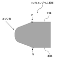
図1に、本発明の実施形態に係るリン化インジウム基板のエッジ部付近の断面模式図を示す。リン化インジウム基板のエッジ部の断面は、図1に示すように長方形の角が削られて(面取りがなされて)、曲線状となっている。本発明において、「エッジ部」とは、リン化インジウム基板の側面、すなわち、主面と裏面を除いた外表面を示し、具体的には、図1に示す主面の端部(平坦な主面が傾斜し始める位置)に位置する点Pから、基板の側面を亘り、裏面の端部(平坦な裏面が傾斜し始める位置)に位置する点Qまでの領域を示す。また、本発明の「エッジ部」はオリエンテーションフラット(OF)、及び、インデックスフラット(IF)も含んでいる。 FIG. 1 shows a schematic cross-sectional view of the vicinity of an edge portion of an indium phosphide substrate according to an embodiment of the present invention. The cross-section of the edge portion of the indium phosphide substrate has a curved shape with the corners of the rectangle cut (chamfered) as shown in FIG. In the present invention, the “edge portion” refers to the side surface of the indium phosphide substrate, that is, the outer surface excluding the main surface and the back surface. The area from the point P located at the position where the surface starts to tilt) to the point Q located at the edge of the back surface (the position where the flat back surface starts to tilt) across the side surface of the substrate. The "edge" of the present invention also includes orientation flats (OF) and index flats (IF).
なお、図1は、本発明の実施形態に係るリン化インジウム基板における主面、裏面、エッジ部を理解するための図面であり、これらがそのまま本発明の実施形態に係るリン化インジウム基板を示すものではない。 FIG. 1 is a drawing for understanding the main surface, the back surface, and the edge portion of the indium phosphide substrate according to the embodiment of the present invention, and shows the indium phosphide substrate according to the embodiment of the present invention as it is. not a thing
本発明の実施形態に係るリン化インジウム基板は、エッジ部の表面粗さについて、エッジ部表面全体において、レーザー顕微鏡によって測定された、二乗平均平方根高さSqが0.15μm以下である。リン化インジウム基板のエッジ部の二乗平均平方根高さSqが0.15μm以下に制御されていることで、面取り以降の加工に用いられる研削砥粒や、研磨液がエッジ部に残留することが抑制される。このため、基板表面に残留物(パーティクル等)が移動することを防ぐことができ、リン化インジウム基板の表面の汚染、及び、基板製造時の歩留まり低下を抑制することができる。基板表面の汚染を防ぐことができると、エピタキシャル成長を実施した後の表面品質が向上する。 In the indium phosphide substrate according to the embodiment of the present invention, the surface roughness of the edge portion has a root-mean-square height Sq of 0.15 μm or less over the entire surface of the edge portion measured with a laser microscope. By controlling the root-mean-square height Sq of the edge portion of the indium phosphide substrate to 0.15 μm or less, grinding abrasive grains and polishing liquid used for processing after chamfering are suppressed from remaining on the edge portion. be done. Therefore, it is possible to prevent residues (particles, etc.) from moving to the substrate surface, thereby suppressing contamination of the surface of the indium phosphide substrate and reduction in yield during substrate manufacturing. The ability to prevent contamination of the substrate surface improves the surface quality after performing epitaxial growth.
本発明の実施形態に係るリン化インジウム基板のエッジ部の二乗平均平方根高さSqは、ISO25178に準拠して測定される、平均面からの標準偏差を表すパラメータである。本発明の実施形態に係るリン化インジウム基板のエッジ部の二乗平均平方根高さSqは、例えば、OLYMPUS社製3D測定レーザー顕微鏡OLS5000を用いて測定することができる。 The root-mean-square height Sq of the edge portion of the indium phosphide substrate according to the embodiment of the present invention is a parameter that represents the standard deviation from the average surface measured in accordance with ISO25178. The root-mean-square height Sq of the edge portion of the indium phosphide substrate according to the embodiment of the present invention can be measured using, for example, a 3D measurement laser microscope OLS5000 manufactured by OLYMPUS.
本発明の実施形態に係るリン化インジウム基板は、エッジ部の表面粗さについて、エッジ部表面全体において、レーザー顕微鏡によって測定された、二乗平均平方根高さSqが0.07μm以下であるのが好ましい。また、本発明の実施形態に係るリン化インジウム基板のエッジ部の当該二乗平均平方根高さSqの下限値は特に限定されないが、0.01μm以上、0.015μm以上であってもよい。 Regarding the surface roughness of the edge portion of the indium phosphide substrate according to the embodiment of the present invention, the root-mean-square height Sq of the entire edge portion surface measured by a laser microscope is preferably 0.07 μm or less. . The lower limit of the root-mean-square height Sq of the edge portion of the indium phosphide substrate according to the embodiment of the present invention is not particularly limited, but may be 0.01 μm or more and 0.015 μm or more.
本発明の実施形態に係るリン化インジウム基板は、エッジ部の表面粗さについて、一方の表面から傾斜した面、及び、一方の表面から傾斜した面が終了する位置から、他方の表面から傾斜した面が終了する位置までの、曲率をもった面を有しており、一方の表面から傾斜した面におけるレーザー顕微鏡によって測定された、二乗平均平方根高さSqが0.15μm以下であり、上述の曲率をもった面におけるレーザー顕微鏡によって測定された、二乗平均平方根高さSqが0.15μm以下であることが好ましい。このような構成によれば、基板表面に残留物(パーティクル等)が移動することをより良好に防ぐことができ、リン化インジウム基板の表面の汚染、及び、基板製造時の歩留まり低下をより良好に抑制することができる。ここで、当該「一方の表面から傾斜した面」は、後述の図3に示す、主面から傾斜した面である測定領域1で示される面であり、当該「一方の表面から傾斜した面が終了する位置から、他方の表面から傾斜した面が終了する位置までの、曲率をもった面」は、後述の図3に示す、測定領域1の主面から傾斜した面が終了する位置から、裏面から傾斜した面が終了する位置までの、曲率をもった面となるエッジ部の円弧領域となる測定領域2で示される面である。 In the indium phosphide substrate according to the embodiment of the present invention, the surface roughness of the edge portion is such that the surface inclined from one surface and the surface inclined from the one surface end from the other surface. It has a surface with a curvature up to the position where the surface terminates, and the root mean square height Sq of the surface inclined from one surface measured by a laser microscope is 0.15 μm or less, and the above-mentioned The root-mean-square height Sq measured with a laser microscope on the curved surface is preferably 0.15 μm or less. According to such a configuration, it is possible to better prevent residues (particles, etc.) from moving to the substrate surface, and to better prevent contamination of the surface of the indium phosphide substrate and decrease in yield during substrate manufacturing. can be suppressed to Here, the "surface inclined from one surface" is a surface shown in the measurement area 1 which is a surface inclined from the main surface shown in FIG. 3 described later, and the "surface inclined from one surface is A surface with a curvature from the end position to the end position of the surface inclined from the other surface is defined as, from the position where the surface inclined from the main surface of the measurement area 1 ends, This is the surface indicated by the measurement area 2, which is the circular arc area of the edge portion that becomes the surface with curvature from the back surface to the end position of the inclined surface.
〔リン化インジウム基板の製造方法〕
次に、本発明の実施形態に係るリン化インジウム基板の製造方法について説明する。
リン化インジウム基板の製造方法としては、まず、公知の方法にてリン化インジウムのインゴットを作製する。
次に、リン化インジウムのインゴットを研削して円筒にする。このとき、ウエハの外周部分の所定位置に、オリエンテーションフラット(OF)、及び、インデックスフラット(IF)を形成してもよい。
次に、研削したリン化インジウムのインゴットから主面及び裏面を有するウエハを切り出す。このとき、リン化インジウムのインゴットの結晶両端を所定の結晶面に沿って、ワイヤーソー等を用いて切断し、複数のウエハを所定の厚さに切り出す。
[Method for producing indium phosphide substrate]
Next, a method for manufacturing an indium phosphide substrate according to an embodiment of the present invention will be described.
As a method for producing an indium phosphide substrate, first, an ingot of indium phosphide is produced by a known method.
The indium phosphide ingot is then ground into a cylinder. At this time, an orientation flat (OF) and an index flat (IF) may be formed at predetermined positions on the outer peripheral portion of the wafer.
Wafers having a primary surface and a back surface are then cut from the ground indium phosphide ingot. At this time, both ends of the crystal of the ingot of indium phosphide are cut along predetermined crystal planes using a wire saw or the like to cut out a plurality of wafers having a predetermined thickness.
次に、ワイヤーソーによる切断工程において生じた加工変質層を除去するために、切断後のウエハに対し、所定のエッチング液により、両面エッチングする(一次エッチング)。ウエハは、エッチング液中にウエハ全体を浸漬することで、エッチングすることができる。 Next, in order to remove the work-affected layer generated in the cutting process with the wire saw, the cut wafer is subjected to both-side etching with a predetermined etchant (primary etching). The wafer can be etched by immersing the entire wafer in an etchant.
次に、ウエハの外周部分の面取りを行う。面取りの後、ウエハの少なくとも一方の表面、好ましくは両面を研磨(ポリッシング)してもよい。当該研磨工程はラッピング工程とも言われ、所定の研磨剤で研磨することで、ウエハの平坦性を保ったままウエハ表面の凹凸を取り除く。 Next, the outer peripheral portion of the wafer is chamfered. After chamfering, at least one surface, preferably both surfaces, of the wafer may be polished. The polishing process is also called a lapping process, and by polishing with a predetermined abrasive, the unevenness of the wafer surface is removed while maintaining the flatness of the wafer.
面取り後、または、面取り後にラッピングを行った場合は当該ラッピング工程の後、面取り後に生じたウエハのエッジ部の表面全体を、番手#4000の研磨フィルムにて研磨する。このとき、ウエハのエッジ部全面を、同じ番手#4000の研磨フィルムにて研磨するため、ウエハのエッジ部全面の粗さが、同様の粗さに制御される。すなわち、当該研磨によって、ウエハのエッジ部の表面粗さについて、エッジ部表面全体において、レーザー顕微鏡によって測定したとき、二乗平均平方根高さSqが0.15μm以下となるように制御する。 After chamfering, or when lapping is performed after chamfering, after the lapping process, the entire surface of the edge portion of the wafer produced after chamfering is polished with a #4000 polishing film. At this time, since the entire surface of the edge portion of the wafer is polished with the same #4000 abrasive film, the roughness of the entire surface of the edge portion of the wafer is controlled to be the same. That is, the polishing controls the surface roughness of the edge portion of the wafer so that the root-mean-square height Sq of the entire edge portion surface is 0.15 μm or less when measured with a laser microscope.
次に、エッジ部の研磨後のウエハに対し、所定のエッチング液により、両面エッチングする(二次エッチング)。ウエハは、前記エッチング液中にウエハ全体を浸漬することで、エッチングすることができる。
次に、ウエハの主面を鏡面研磨用の研磨材で研磨して鏡面に仕上げる。
次に、洗浄を行うことで、本発明の実施形態に係るリン化インジウム基板が製造される。
Next, both sides of the wafer after polishing the edge portion are etched with a predetermined etchant (secondary etching). The wafer can be etched by immersing the entire wafer in the etchant.
Next, the main surface of the wafer is polished with an abrasive for mirror polishing to be mirror-finished.
Next, cleaning is performed to manufacture the indium phosphide substrate according to the embodiment of the present invention.
本発明の実施形態に係るリン化インジウム基板は、上述のように、面取り後の番手#4000の研磨フィルムにて研磨されたエッジ部を有する基板であってもよく、または、研磨フィルムにて研磨された後、エッチング、鏡面研磨、洗浄等を行うことで作製した基板であってもよい。 As described above, the indium phosphide substrate according to the embodiment of the present invention may be a substrate having an edge portion polished with a #4000 polishing film after chamfering, or may be a substrate polished with a polishing film. The substrate may be manufactured by performing etching, mirror-polishing, washing, or the like after being coated.
〔半導体エピタキシャルウエハ〕
本発明の実施形態に係るリン化インジウム基板の主面に対し、公知の方法で半導体薄膜をエピタキシャル成長させることで、エピタキシャル結晶層を形成し、半導体エピタキシャルウエハを作製することができる。当該エピタキシャル成長の例としては、リン化インジウム基板の主面に、InAlAsバッファ層、InGaAsチャネル層、InAlAsスペーサ層、InP電子供給層をエピタキシャル成長させたHEMT構造を形成してもよい。このようなHEMT構造を有する半導体エピタキシャルウエハを作製する場合、一般には、鏡面仕上げしたリン化インジウム基板に、硫酸/過酸化水素水などのエッチング溶液によるエッチング処理を施して、基板表面に付着したケイ素(Si)等の不純物を除去する。このエッチング処理後のリン化インジウム基板の裏面をサセプターに接触させて支持した状態で、リン化インジウム基板の主面に、分子線エピタキシャル成長法(MBE:Molecular Beam Epitaxy)又は有機金属気相成長(MOCVD:Metal Organic Chemical Vapor Deposition)によりエピタキシャル膜を形成する。
[Semiconductor epitaxial wafer]
By epitaxially growing a semiconductor thin film by a known method on the main surface of the indium phosphide substrate according to the embodiment of the present invention, an epitaxial crystal layer can be formed and a semiconductor epitaxial wafer can be produced. As an example of epitaxial growth, a HEMT structure may be formed by epitaxially growing an InAlAs buffer layer, an InGaAs channel layer, an InAlAs spacer layer, and an InP electron supply layer on the main surface of an indium phosphide substrate. When manufacturing a semiconductor epitaxial wafer having such a HEMT structure, generally, a mirror-finished indium phosphide substrate is subjected to an etching treatment with an etching solution such as sulfuric acid/hydrogen peroxide solution to remove silicon attached to the substrate surface. Impurities such as (Si) are removed. With the back surface of the indium phosphide substrate after this etching treatment being supported in contact with the susceptor, the main surface of the indium phosphide substrate is subjected to molecular beam epitaxial growth (MBE) or metal organic chemical vapor deposition (MOCVD). : Metal Organic Chemical Vapor Deposition) to form an epitaxial film.
以下、本発明及びその利点をより良く理解するための実施例を提供するが、本発明はこれらの実施例に限られるものではない。 The following examples are provided for a better understanding of the invention and its advantages, but the invention is not limited to these examples.
(実施例1)
まず、所定の直径で育成したリン化インジウムの単結晶のインゴットを準備した。
次に、リン化インジウムの単結晶のインゴットの外周を研削し、円筒にした。このとき、ウエハの外周部分の所定位置に、オリエンテーションフラット(OF)、及び、インデックスフラット(IF)を形成した。
(Example 1)
First, an ingot of a single crystal of indium phosphide grown with a predetermined diameter was prepared.
Next, the outer periphery of the indium phosphide single crystal ingot was ground to form a cylinder. At this time, an orientation flat (OF) and an index flat (IF) were formed at predetermined positions on the outer periphery of the wafer.
次に、研削したリン化インジウムのインゴットから主面及び裏面を有するウエハを切り出した。このとき、リン化インジウムのインゴットの結晶両端を所定の結晶面に沿って、ワイヤーソーを用いて切断し、複数のウエハを所定の厚さに切り出した。ウエハを切り出す工程では、ワイヤーを往復させながら常に新線を送り続けるとともに、リン化インジウムをワイヤーソーへ移動させた。ここで作製したウエハのウエハ径は、76.2mmであり、ウエハ厚さは750μmであった。 Wafers having a primary surface and a back surface were then cut from the ground indium phosphide ingot. At this time, both ends of the crystal of the ingot of indium phosphide were cut along predetermined crystal planes using a wire saw to cut out a plurality of wafers with a predetermined thickness. In the process of slicing the wafer, the wire was reciprocated and a new wire was constantly fed, and the indium phosphide was moved to the wire saw. The wafer diameter of the wafer produced here was 76.2 mm, and the wafer thickness was 750 μm.
次に、ワイヤーソーによる切断工程において生じた加工変質層を除去するために、切断後のウエハを85質量%のリン酸水溶液及び30質量%の過酸化水素水の混合溶液により、両面からエッチングした(一次エッチング)。ウエハは、エッチング液中にウエハ全体を浸漬することで、エッチングした。 Next, in order to remove the work-affected layer generated in the cutting process with a wire saw, the cut wafer was etched from both sides with a mixed solution of 85% by mass of phosphoric acid aqueous solution and 30% by mass of hydrogen peroxide solution. (primary etching). The wafer was etched by immersing the entire wafer in the etchant.
次に、ウエハの外周部分の面取りを行った。次に、面取り後のウエハの両面を研磨した(ラッピング)。このとき、研磨剤で研磨することで、ウエハの平坦性を保ったままウエハ表面の凹凸を取り除いた。 Next, the outer peripheral portion of the wafer was chamfered. Next, both surfaces of the chamfered wafer were polished (lapping). At this time, the unevenness of the wafer surface was removed while maintaining the flatness of the wafer by polishing with an abrasive.
次に、面取りによって生じたウエハのエッジ部の表面全体を、番手#4000の研磨フィルムに押し当てて研磨した。 Next, the entire surface of the edge portion of the wafer produced by the chamfering was polished by pressing against a #4000 abrasive film.
次に、フィルムによる研磨後のウエハを85質量%のリン酸水溶液、30質量%の過酸化水素水及び超純水の混合溶液により、両面から合計8~15μm厚のエッチング量でエッチングした(二次エッチング)。ウエハは、前記エッチング液中にウエハ全体を浸漬することで、エッチングした。 Next, the wafer after polishing with a film was etched from both sides with a mixed solution of 85% by mass phosphoric acid solution, 30% by mass hydrogen peroxide solution and ultrapure water with a total etching amount of 8 to 15 μm (two secondary etching). The wafer was etched by immersing the entire wafer in the etchant.
次に、ウエハの主面を鏡面研磨用の研磨材で研磨(ポリッシング)して鏡面に仕上げた後、洗浄することでリン化インジウム基板を作製した。 Next, the main surface of the wafer was polished (polished) with an abrasive for mirror polishing to a mirror finish, and then washed to produce an indium phosphide substrate.
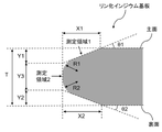
図2に、実施例1で作製されたリン化インジウム基板の平面模式図を示す。また、図3に、実施例1で作製されたリン化インジウム基板のエッジ部付近の断面模式図を示す。図3において、T=650μm、X1=494μm、X2=432μm、Y1=126μm、Y2=108μm、Y3=416μm、R1=167μm、R2=184μm(R1、R2は、エッジ部のラウンド部の曲率半径)、θ1=14.5度、θ2=13.9度(θ1、θ2は、エッジ部の傾斜角度)であった。 FIG. 2 shows a schematic plan view of the indium phosphide substrate produced in Example 1. As shown in FIG. 3 shows a schematic cross-sectional view of the vicinity of the edge portion of the indium phosphide substrate produced in Example 1. As shown in FIG. In FIG. 3, T = 650 µm, X1 = 494 µm, X2 = 432 µm, Y1 = 126 µm, Y2 = 108 µm, Y3 = 416 µm, R1 = 167 µm, R2 = 184 µm (R1 and R2 are the radius of curvature of the rounded portion of the edge). , .theta.1=14.5 degrees, .theta.2=13.9 degrees (.theta.1 and .theta.2 are the inclination angles of the edge portion).
(比較例1)
比較例1として、上述の実施例1において、ラッピング工程の後、研磨フィルムによるエッジ部の研磨を実施せず、二次エッチングを実施した以外は、実施例1と同様にしてリン化インジウム基板を作製した。
(Comparative example 1)
As Comparative Example 1, an indium phosphide substrate was fabricated in the same manner as in Example 1 except that secondary etching was performed without polishing the edge portion with a polishing film after the lapping step in Example 1 described above. made.
(評価)
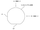
リン化インジウム基板の測定対象となるエッジ部は、図2に示すように、OFの反対側に位置する領域(A-領域)と、IFの反対側に位置する領域(B-領域)とに分け、さらに、図3に示すように、(1)主面から傾斜した面を測定領域1とし、さらに、(2)測定領域1の主面から傾斜した面が終了する位置から、裏面から傾斜した面が終了する位置までの、曲率をもった面となるエッジ部の円弧領域を測定領域2とした。
そして、A-領域における測定領域1を「A-領域1」とし、A-領域における測定領域2を「A-領域2」とし、B-領域における測定領域1を「B-領域1」とし、B-領域における測定領域2を「B-領域2」とした。
(evaluation)
The edge portion of the indium phosphide substrate to be measured is, as shown in FIG. Further, as shown in FIG. 3, (1) a surface inclined from the main surface is defined as the measurement area 1, and (2) the surface inclined from the main surface of the measurement area 1 ends and is inclined from the back surface. A measurement area 2 was defined as an arc area of an edge portion that becomes a surface having a curvature up to a position where the curved surface ends.
Then, the measurement area 1 in the A-area is referred to as "A-area 1", the measurement area 2 in the A-area is referred to as "A-area 2", the measurement area 1 in the B-area is referred to as "B-area 1", The measurement area 2 in the B-area was designated as "B-area 2".
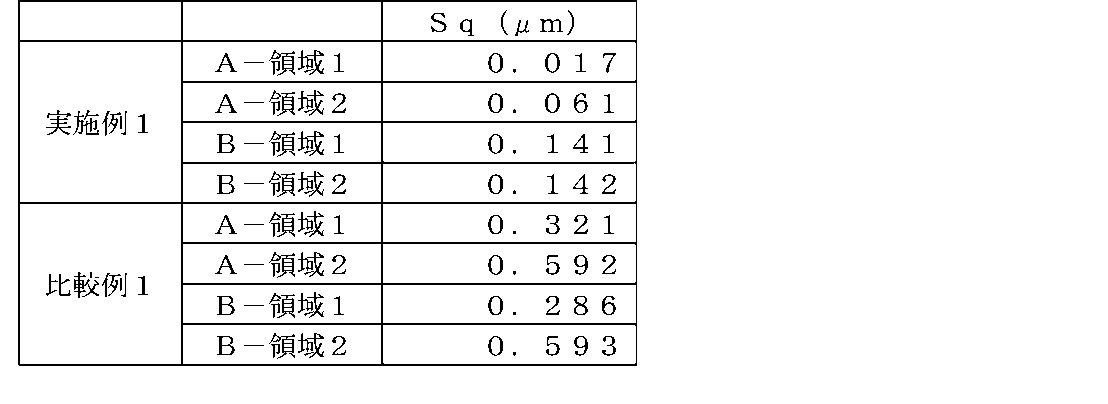
これらエッジ部の合計4箇所の領域(各測定領域サイズ:258μm×258μm)において、それぞれ、OLYMPUS社製3D測定レーザー顕微鏡OLS5000を用いて、二乗平均平方根高さSqを測定した。
なお、エッジ部の曲率を除去して評価するため、カットオフフィルター(Lフィルター:カットする波長20μm)を用いて測定を実施した。
評価結果を表1に示す。
The root-mean-square height Sq was measured using a 3D measuring laser microscope OLS5000 manufactured by OLYMPUS in a total of four areas (measurement area size: 258 μm×258 μm) of these edge portions.
In addition, in order to evaluate by removing the curvature of the edge portion, the measurement was performed using a cut-off filter (L filter: cutting wavelength of 20 μm).
Table 1 shows the evaluation results.
(考察)
実施例1では、基板のエッジ部のA-領域1、2、及び、B-領域1、2の、各表面粗さについて、レーザー顕微鏡によって測定された、二乗平均平方根高さSqが0.15μm以下である、リン化インジウム基板が得られた。基板のエッジ部表面全体において、番手#4000の研磨フィルムにて研磨したものであり、エッジ部表面全体において、測定領域1に対応する傾斜領域は、A-領域1及びB-領域1と同様の表面粗さが得られているものと考えられる。また、エッジ部表面全体において、上述の測定領域2のようなエッジ部の測定領域2に対応する比較的平坦な領域(円弧領域)は、A-領域2及びB-領域2と同様の表面粗さが得られているものと考えられる。
なお、エッジ部の領域1と領域2とで二乗平均平方根高さSqに違いが生じたのは、研磨フィルムにてエッジ部を研磨した後の、鏡面研磨などによる基板表面の研磨による影響が出ているものと考えられる。あくまで、基板のエッジ部表面全体において、番手#4000の研磨フィルムにて研磨した直後であれば、エッジ部表面全体において、どの領域を測定しても、二乗平均平方根高さSqは同様であるものと考えられる。
(Discussion)
In Example 1, the root-mean-square height Sq measured by a laser microscope for each surface roughness of the A-regions 1 and 2 and the B-regions 1 and 2 of the edge portion of the substrate was 0.15 μm. The following indium phosphide substrates were obtained. The entire surface of the edge portion of the substrate was polished with a #4000 polishing film. It is considered that the surface roughness is obtained. Further, on the entire edge portion surface, a relatively flat region (arc region) corresponding to the measurement region 2 of the edge portion, such as the measurement region 2 described above, has the same surface roughness as the A-region 2 and the B-region 2. It is considered that the
The difference in the root-mean-square height Sq between the region 1 and the region 2 of the edge portion is caused by polishing the substrate surface by mirror polishing or the like after polishing the edge portion with a polishing film. It is considered that Root-mean-square height Sq is the same no matter which region is measured on the entire edge surface immediately after polishing the entire edge surface of the substrate with a #4000 polishing film. it is conceivable that.
また、実施例1の基板表面のSi濃度をTOF-SIMS分析で2点測定した結果、80.3(×1010atoms/cm2)、115.8(×1010atoms/cm2)であった。このとき、濃度既知の標準試料をもとに分析装置の感度係数を求めて、Siのイオン強度をIn強度で規格化して定量化した。
TOF-SIMS分析の分析条件は以下の通りである。
装置名:Physical Electronics TRIFT III
イオン源:Au+
一次イオンエネルギー:22kV
分析エリア:25μm×25μm
Further, the Si concentration on the substrate surface of Example 1 was measured at two points by TOF-SIMS analysis, and the results were 80.3 (×10 10 atoms/cm 2 ) and 115.8 (×10 10 atoms/cm 2 ). rice field. At this time, the sensitivity coefficient of the analyzer was obtained based on a standard sample with a known concentration, and the ion intensity of Si was normalized by the In intensity and quantified.
The analysis conditions for TOF-SIMS analysis are as follows.
Device name: Physical Electronics TRIFT III
Ion source: Au +
Primary ion energy: 22 kV
Analysis area: 25 μm×25 μm
比較例1のリン化インジウム基板は、面取り及びラッピング工程後に、基板のエッジ部表面全体において、番手#4000の研磨フィルムにて研磨しなかったため、基板のエッジ部のA-領域1、2、及び、B-領域1、2の、各表面粗さについて、レーザー顕微鏡によって測定された、二乗平均平方根高さSqが0.15μm超であった。 In the indium phosphide substrate of Comparative Example 1, after the chamfering and lapping processes, the entire surface of the edge portion of the substrate was not polished with a #4000 polishing film. , B-regions 1 and 2, the root-mean-square height Sq measured by a laser microscope was greater than 0.15 μm.
Claims (5)
前記基板の一方の表面から傾斜した面、及び、
前記基板の一方の表面から傾斜した面が終了する位置から、前記基板の他方の表面から傾斜した面が終了する位置までの、曲率をもった面
を有し、
前記基板のエッジ部は、前記一方の表面から傾斜した面におけるレーザー顕微鏡によって測定された、二乗平均平方根高さSqが0.15μm以下であり、
前記曲率をもった面におけるレーザー顕微鏡によって測定された、二乗平均平方根高さSqが0.15μm以下である、リン化インジウム基板。 The edge of the board is
a surface slanted from one surface of the substrate; and
having a surface with a curvature from a position where the inclined surface from one surface of the substrate ends to a position where the inclined surface ends from the other surface of the substrate;
The edge portion of the substrate has a root-mean-square height Sq of 0.15 μm or less measured by a laser microscope on a plane inclined from the one surface,
An indium phosphide substrate having a root-mean-square height Sq of 0.15 μm or less as measured by a laser microscope on the curved surface.
前記ウエハの一方の表面から傾斜した面、及び、
前記ウエハの一方の表面から傾斜した面が終了する位置から、前記ウエハの他方の表面から傾斜した面が終了する位置までの、曲率をもった面
を有するように、前記ウエハの外周部分の面取りを行う工程と、
前記面取り後に生じたウエハのエッジ部の表面全体を、番手#4000の研磨フィルムにて研磨する工程と、
前記エッジ部の研磨後のウエハをエッチングする工程と、
を含む、請求項1または2に記載のリン化インジウム基板の製造方法。 The edge of the indium phosphide wafer
a surface slanted from one surface of the wafer; and
A surface with curvature from the position where the inclined surface ends from one surface of the wafer to the position where the inclined surface ends from the other surface of the wafer
chamfering the outer peripheral portion of the wafer so as to have
a step of polishing the entire surface of the edge portion of the wafer generated after the chamfering with a #4000 polishing film;
etching the wafer after polishing the edge portion;
The method for producing an indium phosphide substrate according to claim 1 or 2, comprising:
Priority Applications (7)
| Application Number | Priority Date | Filing Date | Title |
|---|---|---|---|
| JP2020211685A JP7166324B2 (en) | 2020-12-21 | 2020-12-21 | Indium phosphide substrate, method for producing indium phosphide substrate, and semiconductor epitaxial wafer |
| PCT/JP2021/037241 WO2022137728A1 (en) | 2020-12-21 | 2021-10-07 | Indium phosphide substrate, method for manufacturing indium phosphide substrate, and semiconductor epitaxial wafer |
| EP21909886.0A EP4215650A4 (en) | 2020-12-21 | 2021-10-07 | INDIUM PHOSPHIDE SUBSTRATE, METHOD FOR PRODUCING AN INDIUM PHOSPHIDE SUBSTRATE AND EPITATICAL SEMICONDUCTOR WAFER |
| US18/034,327 US20230392289A1 (en) | 2020-12-21 | 2021-10-07 | Indium phosphide substrate, method for manufacturing indium phosphide substrate, and semiconductor epitaxial wafer |
| CN202180054263.9A CN116057212A (en) | 2020-12-21 | 2021-10-07 | Indium phosphide substrate, manufacturing method of indium phosphide substrate, and semiconductor epitaxial wafer |
| TW110138696A TWI771208B (en) | 2020-12-21 | 2021-10-19 | Indium phosphide substrate, manufacturing method of indium phosphide substrate, and semiconductor epitaxial wafer |
| JP2022020684A JP2022098504A (en) | 2020-12-21 | 2022-02-14 | Indium phosphide substrate, manufacturing method of indium phosphide substrate, and semiconductor epitaxial wafer |
Applications Claiming Priority (1)
| Application Number | Priority Date | Filing Date | Title |
|---|---|---|---|
| JP2020211685A JP7166324B2 (en) | 2020-12-21 | 2020-12-21 | Indium phosphide substrate, method for producing indium phosphide substrate, and semiconductor epitaxial wafer |
Related Child Applications (1)
| Application Number | Title | Priority Date | Filing Date |
|---|---|---|---|
| JP2022020684A Division JP2022098504A (en) | 2020-12-21 | 2022-02-14 | Indium phosphide substrate, manufacturing method of indium phosphide substrate, and semiconductor epitaxial wafer |
Publications (2)
| Publication Number | Publication Date |
|---|---|
| JP2022098257A JP2022098257A (en) | 2022-07-01 |
| JP7166324B2 true JP7166324B2 (en) | 2022-11-07 |
Family
ID=82158951
Family Applications (2)
| Application Number | Title | Priority Date | Filing Date |
|---|---|---|---|
| JP2020211685A Active JP7166324B2 (en) | 2020-12-21 | 2020-12-21 | Indium phosphide substrate, method for producing indium phosphide substrate, and semiconductor epitaxial wafer |
| JP2022020684A Withdrawn JP2022098504A (en) | 2020-12-21 | 2022-02-14 | Indium phosphide substrate, manufacturing method of indium phosphide substrate, and semiconductor epitaxial wafer |
Family Applications After (1)
| Application Number | Title | Priority Date | Filing Date |
|---|---|---|---|
| JP2022020684A Withdrawn JP2022098504A (en) | 2020-12-21 | 2022-02-14 | Indium phosphide substrate, manufacturing method of indium phosphide substrate, and semiconductor epitaxial wafer |
Country Status (6)
| Country | Link |
|---|---|
| US (1) | US20230392289A1 (en) |
| EP (1) | EP4215650A4 (en) |
| JP (2) | JP7166324B2 (en) |
| CN (1) | CN116057212A (en) |
| TW (1) | TWI771208B (en) |
| WO (1) | WO2022137728A1 (en) |
Families Citing this family (2)
| Publication number | Priority date | Publication date | Assignee | Title |
|---|---|---|---|---|
| JP7166323B2 (en) * | 2020-12-21 | 2022-11-07 | Jx金属株式会社 | Indium phosphide substrate, method for producing indium phosphide substrate, and semiconductor epitaxial wafer |
| WO2025098595A1 (en) * | 2023-11-07 | 2025-05-15 | Ams-Osram International Gmbh | Growth substrate and method for processing an optoelectronic device |
Citations (6)
| Publication number | Priority date | Publication date | Assignee | Title |
|---|---|---|---|---|
| JP2001135557A (en) | 1999-11-08 | 2001-05-18 | Nikko Materials Co Ltd | Compound semiconductor wafer |
| JP2012129416A (en) | 2010-12-16 | 2012-07-05 | Shin Etsu Handotai Co Ltd | Semiconductor wafer and manufacturing method thereof |
| JP2012174935A (en) | 2011-02-22 | 2012-09-10 | Shin Etsu Handotai Co Ltd | Method of manufacturing epitaxial wafer |
| JP2013153181A (en) | 2009-03-04 | 2013-08-08 | Siltronic Ag | Epitaxially coated silicon wafer and method for producing epitaxially coated silicon wafer |
| JP2019046859A (en) | 2017-08-30 | 2019-03-22 | 昭和電工株式会社 | SiC EPITAXIAL WAFER AND MANUFACTURING METHOD THEREOF |
| JP2019219495A (en) | 2018-06-19 | 2019-12-26 | 信越化学工業株式会社 | Evaluation method of photomask blank-related substrate |
Family Cites Families (14)
| Publication number | Priority date | Publication date | Assignee | Title |
|---|---|---|---|---|
| JP4207976B2 (en) * | 2006-05-17 | 2009-01-14 | 住友電気工業株式会社 | Method for surface treatment of compound semiconductor substrate and method for producing compound semiconductor crystal |
| JPS6117257A (en) | 1984-07-04 | 1986-01-25 | Victor Co Of Japan Ltd | Magnetic recording and reproducing device |
| JPH11204493A (en) * | 1998-01-09 | 1999-07-30 | Komatsu Electron Metals Co Ltd | Method for manufacturing semiconductor wafer |
| JP3534115B1 (en) * | 2003-04-02 | 2004-06-07 | 住友電気工業株式会社 | Edge-polished nitride semiconductor substrate, edge-polished GaN free-standing substrate, and edge processing method for nitride semiconductor substrate |
| DE102005034120B4 (en) * | 2005-07-21 | 2013-02-07 | Siltronic Ag | Method for producing a semiconductor wafer |
| JP2007042748A (en) * | 2005-08-01 | 2007-02-15 | Hitachi Cable Ltd | Compound semiconductor wafer |
| KR20080013059A (en) * | 2006-08-07 | 2008-02-13 | 삼성전자주식회사 | Wafer Inspection Equipment and Method of CMP Processing Equipment |
| JP4395812B2 (en) * | 2008-02-27 | 2010-01-13 | 住友電気工業株式会社 | Nitride semiconductor wafer-processing method |
| JP5644401B2 (en) * | 2010-11-15 | 2014-12-24 | 株式会社Sumco | Epitaxial wafer manufacturing method and epitaxial wafer |
| WO2012102313A1 (en) * | 2011-01-26 | 2012-08-02 | 旭硝子株式会社 | Method for manufacturing photomask |
| EP4174913A1 (en) * | 2015-02-09 | 2023-05-03 | Sumitomo Electric Industries, Ltd. | Indium phosphorus substrate, indium phosphorus substrate inspection method, and indium phosphorus substrate manufacturing method |
| EP3476983A4 (en) * | 2017-04-28 | 2020-04-01 | JX Nippon Mining & Metals Corporation | SEMICONDUCTOR WAFER AND METHOD FOR POLISHING A SEMICONDUCTOR WAFER |
| JP7381214B2 (en) * | 2019-03-27 | 2023-11-15 | 株式会社東京精密 | Chamfering device with blast unit |
| JP7166323B2 (en) * | 2020-12-21 | 2022-11-07 | Jx金属株式会社 | Indium phosphide substrate, method for producing indium phosphide substrate, and semiconductor epitaxial wafer |
-
2020
- 2020-12-21 JP JP2020211685A patent/JP7166324B2/en active Active
-
2021
- 2021-10-07 WO PCT/JP2021/037241 patent/WO2022137728A1/en not_active Ceased
- 2021-10-07 US US18/034,327 patent/US20230392289A1/en active Pending
- 2021-10-07 EP EP21909886.0A patent/EP4215650A4/en active Pending
- 2021-10-07 CN CN202180054263.9A patent/CN116057212A/en active Pending
- 2021-10-19 TW TW110138696A patent/TWI771208B/en active
-
2022
- 2022-02-14 JP JP2022020684A patent/JP2022098504A/en not_active Withdrawn
Patent Citations (6)
| Publication number | Priority date | Publication date | Assignee | Title |
|---|---|---|---|---|
| JP2001135557A (en) | 1999-11-08 | 2001-05-18 | Nikko Materials Co Ltd | Compound semiconductor wafer |
| JP2013153181A (en) | 2009-03-04 | 2013-08-08 | Siltronic Ag | Epitaxially coated silicon wafer and method for producing epitaxially coated silicon wafer |
| JP2012129416A (en) | 2010-12-16 | 2012-07-05 | Shin Etsu Handotai Co Ltd | Semiconductor wafer and manufacturing method thereof |
| JP2012174935A (en) | 2011-02-22 | 2012-09-10 | Shin Etsu Handotai Co Ltd | Method of manufacturing epitaxial wafer |
| JP2019046859A (en) | 2017-08-30 | 2019-03-22 | 昭和電工株式会社 | SiC EPITAXIAL WAFER AND MANUFACTURING METHOD THEREOF |
| JP2019219495A (en) | 2018-06-19 | 2019-12-26 | 信越化学工業株式会社 | Evaluation method of photomask blank-related substrate |
Also Published As
| Publication number | Publication date |
|---|---|
| WO2022137728A1 (en) | 2022-06-30 |
| TWI771208B (en) | 2022-07-11 |
| EP4215650A4 (en) | 2024-10-16 |
| EP4215650A1 (en) | 2023-07-26 |
| US20230392289A1 (en) | 2023-12-07 |
| CN116057212A (en) | 2023-05-02 |
| TW202225090A (en) | 2022-07-01 |
| JP2022098257A (en) | 2022-07-01 |
| JP2022098504A (en) | 2022-07-01 |
Similar Documents
| Publication | Publication Date | Title |
|---|---|---|
| JP7158594B2 (en) | indium phosphide substrate | |
| CN113207310A (en) | Indium phosphide substrate, semiconductor epitaxial wafer, and manufacturing method of indium phosphide substrate | |
| JP7166324B2 (en) | Indium phosphide substrate, method for producing indium phosphide substrate, and semiconductor epitaxial wafer | |
| JP6761915B1 (en) | Method for manufacturing indium phosphide substrate, semiconductor epitaxial wafer, and indium phosphide substrate | |
| JP6761916B1 (en) | Method for manufacturing indium phosphide substrate, semiconductor epitaxial wafer, and indium phosphide substrate | |
| JP7166323B2 (en) | Indium phosphide substrate, method for producing indium phosphide substrate, and semiconductor epitaxial wafer | |
| TWI810847B (en) | Indium Phosphide Substrate | |
| US12065759B2 (en) | Indium phosphide substrate | |
| JP7713056B1 (en) | Indium phosphide substrates and semiconductor epitaxial wafers |
Legal Events
| Date | Code | Title | Description |
|---|---|---|---|
| A621 | Written request for application examination |
Free format text: JAPANESE INTERMEDIATE CODE: A621 Effective date: 20210311 |
|
| A871 | Explanation of circumstances concerning accelerated examination |
Free format text: JAPANESE INTERMEDIATE CODE: A871 Effective date: 20210311 |
|
| A975 | Report on accelerated examination |
Free format text: JAPANESE INTERMEDIATE CODE: A971005 Effective date: 20210407 |
|
| A131 | Notification of reasons for refusal |
Free format text: JAPANESE INTERMEDIATE CODE: A131 Effective date: 20210420 |
|
| A521 | Request for written amendment filed |
Free format text: JAPANESE INTERMEDIATE CODE: A523 Effective date: 20210608 |
|
| A131 | Notification of reasons for refusal |
Free format text: JAPANESE INTERMEDIATE CODE: A131 Effective date: 20210907 |
|
| A521 | Request for written amendment filed |
Free format text: JAPANESE INTERMEDIATE CODE: A523 Effective date: 20211101 |
|
| A02 | Decision of refusal |
Free format text: JAPANESE INTERMEDIATE CODE: A02 Effective date: 20211130 |
|
| A521 | Request for written amendment filed |
Free format text: JAPANESE INTERMEDIATE CODE: A523 Effective date: 20220214 |
|
| C60 | Trial request (containing other claim documents, opposition documents) |
Free format text: JAPANESE INTERMEDIATE CODE: C60 Effective date: 20220214 |
|
| A911 | Transfer to examiner for re-examination before appeal (zenchi) |
Free format text: JAPANESE INTERMEDIATE CODE: A911 Effective date: 20220224 |
|
| C21 | Notice of transfer of a case for reconsideration by examiners before appeal proceedings |
Free format text: JAPANESE INTERMEDIATE CODE: C21 Effective date: 20220301 |
|
| A912 | Re-examination (zenchi) completed and case transferred to appeal board |
Free format text: JAPANESE INTERMEDIATE CODE: A912 Effective date: 20220401 |
|
| C211 | Notice of termination of reconsideration by examiners before appeal proceedings |
Free format text: JAPANESE INTERMEDIATE CODE: C211 Effective date: 20220405 |
|
| C22 | Notice of designation (change) of administrative judge |
Free format text: JAPANESE INTERMEDIATE CODE: C22 Effective date: 20220726 |
|
| C22 | Notice of designation (change) of administrative judge |
Free format text: JAPANESE INTERMEDIATE CODE: C22 Effective date: 20220823 |
|
| C23 | Notice of termination of proceedings |
Free format text: JAPANESE INTERMEDIATE CODE: C23 Effective date: 20220913 |
|
| C03 | Trial/appeal decision taken |
Free format text: JAPANESE INTERMEDIATE CODE: C03 Effective date: 20221011 |
|
| C30A | Notification sent |
Free format text: JAPANESE INTERMEDIATE CODE: C3012 Effective date: 20221011 |
|
| A61 | First payment of annual fees (during grant procedure) |
Free format text: JAPANESE INTERMEDIATE CODE: A61 Effective date: 20221025 |
|
| R151 | Written notification of patent or utility model registration |
Ref document number: 7166324 Country of ref document: JP Free format text: JAPANESE INTERMEDIATE CODE: R151 |
|
| R250 | Receipt of annual fees |
Free format text: JAPANESE INTERMEDIATE CODE: R250 |