JP7159190B2 - システム特徴をセキュアに分離するためのシステムおよび方法 - Google Patents
システム特徴をセキュアに分離するためのシステムおよび方法 Download PDFInfo
- Publication number
- JP7159190B2 JP7159190B2 JP2019552241A JP2019552241A JP7159190B2 JP 7159190 B2 JP7159190 B2 JP 7159190B2 JP 2019552241 A JP2019552241 A JP 2019552241A JP 2019552241 A JP2019552241 A JP 2019552241A JP 7159190 B2 JP7159190 B2 JP 7159190B2
- Authority
- JP
- Japan
- Prior art keywords
- lockdown
- signal
- hardware logic
- state
- volatile memory
- Prior art date
- Legal status (The legal status is an assumption and is not a legal conclusion. Google has not performed a legal analysis and makes no representation as to the accuracy of the status listed.)
- Active
Links
Images


Classifications
-
- G—PHYSICS
- G06—COMPUTING; CALCULATING OR COUNTING
- G06F—ELECTRIC DIGITAL DATA PROCESSING
- G06F21/00—Security arrangements for protecting computers, components thereof, programs or data against unauthorised activity
- G06F21/70—Protecting specific internal or peripheral components, in which the protection of a component leads to protection of the entire computer
- G06F21/71—Protecting specific internal or peripheral components, in which the protection of a component leads to protection of the entire computer to assure secure computing or processing of information
-
- G—PHYSICS
- G06—COMPUTING; CALCULATING OR COUNTING
- G06F—ELECTRIC DIGITAL DATA PROCESSING
- G06F3/00—Input arrangements for transferring data to be processed into a form capable of being handled by the computer; Output arrangements for transferring data from processing unit to output unit, e.g. interface arrangements
- G06F3/06—Digital input from, or digital output to, record carriers, e.g. RAID, emulated record carriers or networked record carriers
- G06F3/0601—Interfaces specially adapted for storage systems
- G06F3/0628—Interfaces specially adapted for storage systems making use of a particular technique
- G06F3/0629—Configuration or reconfiguration of storage systems
- G06F3/0634—Configuration or reconfiguration of storage systems by changing the state or mode of one or more devices
-
- G—PHYSICS
- G06—COMPUTING; CALCULATING OR COUNTING
- G06F—ELECTRIC DIGITAL DATA PROCESSING
- G06F12/00—Accessing, addressing or allocating within memory systems or architectures
- G06F12/14—Protection against unauthorised use of memory or access to memory
- G06F12/1416—Protection against unauthorised use of memory or access to memory by checking the object accessibility, e.g. type of access defined by the memory independently of subject rights
- G06F12/1425—Protection against unauthorised use of memory or access to memory by checking the object accessibility, e.g. type of access defined by the memory independently of subject rights the protection being physical, e.g. cell, word, block
- G06F12/1433—Protection against unauthorised use of memory or access to memory by checking the object accessibility, e.g. type of access defined by the memory independently of subject rights the protection being physical, e.g. cell, word, block for a module or a part of a module
-
- G—PHYSICS
- G06—COMPUTING; CALCULATING OR COUNTING
- G06F—ELECTRIC DIGITAL DATA PROCESSING
- G06F21/00—Security arrangements for protecting computers, components thereof, programs or data against unauthorised activity
- G06F21/70—Protecting specific internal or peripheral components, in which the protection of a component leads to protection of the entire computer
- G06F21/82—Protecting input, output or interconnection devices
- G06F21/85—Protecting input, output or interconnection devices interconnection devices, e.g. bus-connected or in-line devices
-
- G—PHYSICS
- G06—COMPUTING; CALCULATING OR COUNTING
- G06F—ELECTRIC DIGITAL DATA PROCESSING
- G06F3/00—Input arrangements for transferring data to be processed into a form capable of being handled by the computer; Output arrangements for transferring data from processing unit to output unit, e.g. interface arrangements
- G06F3/06—Digital input from, or digital output to, record carriers, e.g. RAID, emulated record carriers or networked record carriers
- G06F3/0601—Interfaces specially adapted for storage systems
- G06F3/0602—Interfaces specially adapted for storage systems specifically adapted to achieve a particular effect
- G06F3/062—Securing storage systems
- G06F3/0622—Securing storage systems in relation to access
-
- G—PHYSICS
- G06—COMPUTING; CALCULATING OR COUNTING
- G06F—ELECTRIC DIGITAL DATA PROCESSING
- G06F3/00—Input arrangements for transferring data to be processed into a form capable of being handled by the computer; Output arrangements for transferring data from processing unit to output unit, e.g. interface arrangements
- G06F3/06—Digital input from, or digital output to, record carriers, e.g. RAID, emulated record carriers or networked record carriers
- G06F3/0601—Interfaces specially adapted for storage systems
- G06F3/0628—Interfaces specially adapted for storage systems making use of a particular technique
- G06F3/0655—Vertical data movement, i.e. input-output transfer; data movement between one or more hosts and one or more storage devices
- G06F3/0656—Data buffering arrangements
-
- G—PHYSICS
- G06—COMPUTING; CALCULATING OR COUNTING
- G06F—ELECTRIC DIGITAL DATA PROCESSING
- G06F3/00—Input arrangements for transferring data to be processed into a form capable of being handled by the computer; Output arrangements for transferring data from processing unit to output unit, e.g. interface arrangements
- G06F3/06—Digital input from, or digital output to, record carriers, e.g. RAID, emulated record carriers or networked record carriers
- G06F3/0601—Interfaces specially adapted for storage systems
- G06F3/0628—Interfaces specially adapted for storage systems making use of a particular technique
- G06F3/0655—Vertical data movement, i.e. input-output transfer; data movement between one or more hosts and one or more storage devices
- G06F3/0659—Command handling arrangements, e.g. command buffers, queues, command scheduling
-
- G—PHYSICS
- G06—COMPUTING; CALCULATING OR COUNTING
- G06F—ELECTRIC DIGITAL DATA PROCESSING
- G06F3/00—Input arrangements for transferring data to be processed into a form capable of being handled by the computer; Output arrangements for transferring data from processing unit to output unit, e.g. interface arrangements
- G06F3/06—Digital input from, or digital output to, record carriers, e.g. RAID, emulated record carriers or networked record carriers
- G06F3/0601—Interfaces specially adapted for storage systems
- G06F3/0668—Interfaces specially adapted for storage systems adopting a particular infrastructure
- G06F3/0671—In-line storage system
- G06F3/0673—Single storage device
- G06F3/0679—Non-volatile semiconductor memory device, e.g. flash memory, one time programmable memory [OTP]
-
- G—PHYSICS
- G06—COMPUTING; CALCULATING OR COUNTING
- G06F—ELECTRIC DIGITAL DATA PROCESSING
- G06F2212/00—Indexing scheme relating to accessing, addressing or allocation within memory systems or architectures
- G06F2212/10—Providing a specific technical effect
- G06F2212/1052—Security improvement
Landscapes
- Engineering & Computer Science (AREA)
- Theoretical Computer Science (AREA)
- Physics & Mathematics (AREA)
- General Engineering & Computer Science (AREA)
- General Physics & Mathematics (AREA)
- Human Computer Interaction (AREA)
- Computer Hardware Design (AREA)
- Computer Security & Cryptography (AREA)
- Software Systems (AREA)
- Mathematical Physics (AREA)
- Storage Device Security (AREA)
- Microcomputers (AREA)
- Logic Circuits (AREA)
Description
本発明は、コンピュータセキュリティに関する。特に、本発明は、1つまたは複数のシステム特徴の選択的分離に関する。
この出願は、2017年3月22日に出願された米国仮出願第15/466,484号の利益と優先権を主張し、その全体は、参照によりここに組み込まれる。
コンピューティングシステムは、多くのコンポーネントおよび特徴を含む。コンポーネントは、ユニバーサルシリアルバス(USB)といったインターフェース、不揮発性メモリといったハードウェア、およびリモートサーバ管理のために使用される管理コントローラといった統合されたデバイスを含む。特徴は、コンポーネントがターンオンにされもしくはターンオフにされているかどうか、コンポーネントがリセット状態に保持されているか、またはコンポーネントがクロックにアクセスし得るかといった、コンポーネントの一部または状態を含む。
実施形態は、添付の図面の図において限定ではなく例として示される。本開示における「ある」または「1つ」の実施形態への言及は、必ずしも同じ実施形態への言及ではなく、少なくとも一つを意味することに留意されたい。
以下の説明では、説明の目的で、完全な理解を提供するために多くの特定の詳細が述べられる。1つまたは複数の実施形態は、これらの特定の詳細なしで、実施されることができる。1つの実施形態で説明される特徴は、異なる実施形態で説明される特徴と組み合わせることができる。いくつかの例では、本発明を不必要に不明瞭にすることを避けるために、ブロック図形式を参照して既知の構造およびデバイスを説明する。
2. ロックダウン構成にあるシステム
3. 非ロックダウン構成にあるシステム
4. システム特徴の分離
5. リモート再構成
6. その他、拡張
7. ハードウェア概要
1つまたは複数の実施形態は、システム特徴を選択的におよびセキュアに分離することを含む。システムは、1つまたは複数の特徴を含む。1つまたは複数のこれらの特徴は、無効状態にあり得、または有効状態にあり得る。システムは、ロックダウン状態へと構成されることができ、その状態では特定のシステム特徴の無効にされた状態または有効にされた状態は、変えられることができない。
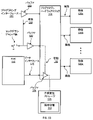
図1Aは、1つまたは複数の実施形態に従う、ロックダウン構成におけるシステムを示す。プログラマブルハードウェアロジック110は、不揮発性ストレージ116内に格納された信号状態118に基づき機能を実装する。システムはさらに、プログラミングインターフェース102、ロックダウンジャンパ104、ベースボード管理コントローラ(BMC)112、および特徴120a-120nを含む。システムはさらに、マザーボード(図示されない)を含む。1つまたは複数の実施形態では、システムは、図1A内に示されたコンポーネントよりも多いまたは少ないコンポーネントを含み得る。図1A内に示されたコンポーネントは、互いにローカルにまたはリモートにあり得る。図1A内に示されたコンポーネントは、ソフトウェアおよび/またはハードウェア内に実装され得る。各コンポーネントは、複数のアプリケーションおよび/またはマシンにわたって分散され得る。複数のコンポーネントは、1つのアプリケーションおよび/またはマシンへと組み合わされ得る。1つのコンポーネントに対して記載された動作は、代わりに別のコンポーネントによって行われ得る。
図1Bは、1つまたは複数の実施形態に従う、非ロックダウン構成にあるシステムを示す。プログラミングインターフェース102と、BMC112と、データインターフェース114と、バッファ108、122、126と、プログラマブルハードウェアロジック110と、不揮発性ストレージ116と、信号状態118と、特徴120a-120nとは、上述のセクション2において図1Aを参照して説明されたが、以下に記述するように異なって実装されまたは異なって動作し得る。図1Bでは、システムは、非ロックダウン状態にある。ロックダウンジャンパは、非ロックダウン状態において挿入されない。図1B内に示されたコンポーネントは、互いにローカルにまたはリモートにあり得る。図1B内に示されたコンポーネントは、ソフトウェアおよび/またはハードウェア内に実装され得る。各コンポーネントは、複数のアプリケーションおよび/またはマシンにわたって分散され得る。複数のコンポーネントは、1つのアプリケーションおよび/またはマシンへと組み合わされ得る。1つのコンポーネントに対して記載された動作は、代わりに別のコンポーネントによって行われ得る。
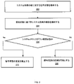
図2は、1つまたは複数の実施形態に従う、システム特徴を分離するための例示的動作の組を示す。図2において示された1つまたは複数の動作は、変形され、再配置され、またはすべて削除され得る。従って、図2に示される特定の動作シーケンスは、1つ以上の実施形態の範囲を限定するものとして解釈されるべきではない。
実施形態では、システムは、ロックダウン状態へとまたはそれからリモートに再構成されることができる。ロックダウンは、ジャンパを用いてアサートされる必要はない。この場合、ロックダウンは、システム内の信頼されたエンティティを使用してアサートされ、これは、システムのリモート管理を可能とする。
実施形態は、ハードウェアプロセッサを含み、本明細書に記載および/または添付の特許請求の範囲のいずれかに列挙される動作のいずれかを実行するように構成される1つまたは複数のデバイスを有するシステムに向けられる。
1つの実施形態に従って、ここで説明される技法は、1つまたは複数の特定用途のコンピューティングデバイスによって実装される。特定用途コンピューティングデバイスは、技法を実行するために有線であり得、または技法を実行するために永続的にプログラムされた1つまたは複数の特定用途向け集積回路(ASIC)、フィールドプログラマブルゲートアレイ(FPGA)、またはネットワーク処理ユニット(NPU)といったデジタル電子デバイスを含み得、またはファームウェア、メモリ、他のストレージ、または組み合わせにおけるプログラム命令に従って技法を実行するようにプログラムされた1つまたは複数の汎用ハードウェアプロセッサを含み得る。そのような特定用途コンピューティングデバイスは、カスタム有線ロジック、ASIC、FPGA、またはNPUをカスタムプログラミングと組み合わせて、技法を実現し得る。特定用途コンピューティングデバイスは、デスクトップコンピュータシステム、ポータブルコンピューターシステム、ハンドヘルドデバイス、ネットワークデバイス、または技法を実装するための有線および/またはプログラムロジックを組み込んだ任意の他のデバイスであり得る。
Claims (10)
- システムであって、
1つまたは複数のシステム特徴の組の各々に対する信号のための信号状態の組を格納する不揮発性メモリを備え、
前記システムは、
(a)前記不揮発性メモリ内に格納された前記信号状態の組が変更されることができないロックダウン状態と、
(b)前記不揮発性メモリ内に格納された前記信号状態の組が変更されることができる非ロックダウン状態とに構成可能なハードウェアと、
前記信号状態に基づき前記システム特徴の組の機能を構成する、ハードウェアロジックとを備え、
前記ロックダウン状態と前記非ロックダウン状態との間の変化は、前記システムの物理的操作なしに引き起こされることができず、
前記システムの前記物理的操作は、(a)前記システム内に備えられたマザーボード上の2つのピンを接続するためにジャンパを追加すること、または(b)前記ジャンパを除去して、前記システム内に備えられたマザーボード上の2つのピンを切断することを備える、システム。 - システムであって、
1つまたは複数のシステム特徴の組の各々に対する信号のための信号状態の組を格納する不揮発性メモリを備え、
前記システムは、
(a)前記不揮発性メモリ内に格納された前記信号状態の組が変更されることができないロックダウン状態と、
(b)前記不揮発性メモリ内に格納された前記信号状態の組が変更されることができる非ロックダウン状態とに構成可能なハードウェアと、
前記信号状態に基づき前記システム特徴の組の機能を構成する、ハードウェアロジックとを備え、
前記ロックダウン状態と前記非ロックダウン状態との間の変化は、前記システム内に備えられた信頼されたエンティティを介する前記システムの遠隔操作を用いて引き起こされることができる、システム。 - 前記ハードウェアロジックは、前記非ロックダウン状態の間に再プログラムされることができ、前記ハードウェアロジックは、前記ロックダウン状態の間に再プログラムされることができない、請求項1または2に記載のシステム。
- 前記ハードウェアロジックは、前記ロックダウン状態または前記非ロックダウン状態のいずれの間にも再プログラムされることができないハード化されたロジックを備える、請求項1または2に記載のシステム。
- 前記システムは、前記ハードウェアが前記非ロックダウン状態にあるときに前記不揮発性メモリ内に格納された前記信号状態の組を変更するための機能を含む前記ハードウェアロジックの外部のコントローラをさらに備え、前記コントローラは、前記ハードウェアが前記ロックダウン状態にあるときに前記不揮発性メモリ内に格納された前記信号状態の組を変更することができない、請求項1から請求項4のいずれか1項に記載のシステム。
- 前記コントローラは、ベースボード管理コントローラ(BMC)である、請求項5に記載のシステム。
- 前記コントローラは、前記ハードウェアが前記ロックダウン状態にあるときに前記不揮発性メモリ内に格納された前記信号状態の組を読み込むための機能を含む、請求項5に記載のシステム。
- 前記不揮発性メモリは、前記ハードウェアロジックのみを介してアクセス可能である、請求項1から請求項7のいずれか1項に記載のシステム。
- 方法であって、
システムのハードウェアロジックが、前記システムの不揮発性メモリに、1つまたは複数のシステム特徴の組の各々に対する信号のための信号状態の組を格納するステップと、
前記システムの物理的操作に基づいて無効信号または有効信号を伝送する信号伝送手段が、前記システムのハードウェアを、(a)前記不揮発性メモリ内に格納された前記信号状態の組が変更されることができないロックダウン状態と、(b)前記不揮発性メモリ内に格納された前記信号状態の組が変更されることができる非ロックダウン状態との1つに構成するステップと、
前記システムの前記ハードウェアロジックが、前記信号状態に基づき前記システム特徴の組の機能を構成するステップとを備え、
前記ロックダウン状態と前記非ロックダウン状態との間の変化は、前記システムの前記物理的操作なしに引き起こされることができず、
前記システムの前記物理的操作は、(a)前記システム内に備えられたマザーボード上の2つのピンを接続するためにジャンパを追加すること、または(b)前記ジャンパを除去して、前記システム内に備えられたマザーボード上の2つのピンを切断することを備える、方法。 - 方法であって、
システムのハードウェアロジックが、前記システムの不揮発性メモリに、1つまたは複数のシステム特徴の組の各々に対する信号のための信号状態の組を格納するステップと、
前記システム内に備えられた信頼されたエンティティが、前記システムのハードウェアを、(a)前記不揮発性メモリ内に格納された前記信号状態の組が変更されることができないロックダウン状態と、(b)前記不揮発性メモリ内に格納された前記信号状態の組が変更されることができる非ロックダウン状態との1つに構成するステップと、
前記システムの前記ハードウェアロジックが、前記信号状態に基づき前記システム特徴の組の機能を構成するステップとを備え、
前記ロックダウン状態と前記非ロックダウン状態との間の変化は、前記システム内に備えられた前記信頼されたエンティティを介する前記システムの遠隔操作を用いて引き起こされることができる、方法。
Priority Applications (1)
| Application Number | Priority Date | Filing Date | Title |
|---|---|---|---|
| JP2022117179A JP7441896B2 (ja) | 2017-03-22 | 2022-07-22 | システム特徴をセキュアに分離するためのシステムおよび方法 |
Applications Claiming Priority (3)
| Application Number | Priority Date | Filing Date | Title |
|---|---|---|---|
| US15/466,484 US10585608B2 (en) | 2017-03-22 | 2017-03-22 | System and method for securely isolating a system feature |
| US15/466,484 | 2017-03-22 | ||
| PCT/US2017/064824 WO2018174971A1 (en) | 2017-03-22 | 2017-12-06 | System and method for securely isolating a system feature |
Related Child Applications (1)
| Application Number | Title | Priority Date | Filing Date |
|---|---|---|---|
| JP2022117179A Division JP7441896B2 (ja) | 2017-03-22 | 2022-07-22 | システム特徴をセキュアに分離するためのシステムおよび方法 |
Publications (3)
| Publication Number | Publication Date |
|---|---|
| JP2020514927A JP2020514927A (ja) | 2020-05-21 |
| JP2020514927A5 JP2020514927A5 (ja) | 2021-01-21 |
| JP7159190B2 true JP7159190B2 (ja) | 2022-10-24 |
Family
ID=60782386
Family Applications (2)
| Application Number | Title | Priority Date | Filing Date |
|---|---|---|---|
| JP2019552241A Active JP7159190B2 (ja) | 2017-03-22 | 2017-12-06 | システム特徴をセキュアに分離するためのシステムおよび方法 |
| JP2022117179A Active JP7441896B2 (ja) | 2017-03-22 | 2022-07-22 | システム特徴をセキュアに分離するためのシステムおよび方法 |
Family Applications After (1)
| Application Number | Title | Priority Date | Filing Date |
|---|---|---|---|
| JP2022117179A Active JP7441896B2 (ja) | 2017-03-22 | 2022-07-22 | システム特徴をセキュアに分離するためのシステムおよび方法 |
Country Status (5)
| Country | Link |
|---|---|
| US (1) | US10585608B2 (ja) |
| EP (1) | EP3602390B1 (ja) |
| JP (2) | JP7159190B2 (ja) |
| CN (1) | CN110462624B (ja) |
| WO (1) | WO2018174971A1 (ja) |
Families Citing this family (1)
| Publication number | Priority date | Publication date | Assignee | Title |
|---|---|---|---|---|
| US11099922B2 (en) * | 2019-08-12 | 2021-08-24 | Dell Products L.P. | System and method for isolating a failed card |
Citations (2)
| Publication number | Priority date | Publication date | Assignee | Title |
|---|---|---|---|---|
| JP2000267847A (ja) | 1999-03-18 | 2000-09-29 | Miyazaki Oki Electric Co Ltd | セキュリティシステム |
| JP2008305401A (ja) | 2007-06-05 | 2008-12-18 | Xerox Corp | 製品の機能をプログラムする方法、及び製品の機能をプログラムするための装置 |
Family Cites Families (17)
| Publication number | Priority date | Publication date | Assignee | Title |
|---|---|---|---|---|
| US5524008A (en) * | 1995-03-21 | 1996-06-04 | National Semiconductor Corporation | Generating real-time events in a TDMA digital wireless communications system |
| US7149854B2 (en) * | 2001-05-10 | 2006-12-12 | Advanced Micro Devices, Inc. | External locking mechanism for personal computer memory locations |
| JP4256859B2 (ja) * | 2005-04-21 | 2009-04-22 | シャープ株式会社 | 半導体記憶装置 |
| US20080005462A1 (en) * | 2006-06-30 | 2008-01-03 | Mosaid Technologies Incorporated | Method of configuring non-volatile memory for a hybrid disk drive |
| US7594144B2 (en) * | 2006-08-14 | 2009-09-22 | International Business Machines Corporation | Handling fatal computer hardware errors |
| KR100833189B1 (ko) * | 2006-11-03 | 2008-05-28 | 삼성전자주식회사 | 불휘발성 메모리 장치 및 불휘발성 메모리 장치의환경설정정보 설정 방법 |
| US7574576B2 (en) * | 2006-12-22 | 2009-08-11 | Spansion Llc | Semiconductor device and method of controlling the same |
| US8392683B1 (en) * | 2009-11-30 | 2013-03-05 | Micron Technology, Inc. | Dynamic range unlock or lock memory device and method to operate the same |
| US10771448B2 (en) * | 2012-08-10 | 2020-09-08 | Cryptography Research, Inc. | Secure feature and key management in integrated circuits |
| US9521032B1 (en) * | 2013-03-14 | 2016-12-13 | Amazon Technologies, Inc. | Server for authentication, authorization, and accounting |
| US20140359196A1 (en) * | 2013-05-31 | 2014-12-04 | Daniel J. Ragland | On-the-fly performance adjustment for solid state storage devices |
| US9658787B2 (en) * | 2014-02-26 | 2017-05-23 | Macronix International Co., Ltd. | Nonvolatile memory data protection using nonvolatile protection codes and volatile mask codes |
| US20150381368A1 (en) * | 2014-06-27 | 2015-12-31 | William A. Stevens, Jr. | Technologies for secure offline activation of hardware features |
| US9747739B2 (en) * | 2014-08-18 | 2017-08-29 | Noke, Inc. | Wireless locking device |
| KR102604892B1 (ko) * | 2014-09-17 | 2023-11-21 | 크라이프토그라피 리서치, 인코포레이티드 | 집적 회로를 위한 상이한 엔티티들의 특권들의 관리 |
| JP6492835B2 (ja) * | 2015-03-23 | 2019-04-03 | 富士通クライアントコンピューティング株式会社 | ポータブル機器、及び情報処理装置 |
| CN106227636A (zh) * | 2016-07-20 | 2016-12-14 | 国网安徽省电力公司信息通信分公司 | 一种基于ipmi的数据中心带外管理系统 |
-
2017
- 2017-03-22 US US15/466,484 patent/US10585608B2/en active Active
- 2017-12-06 CN CN201780088688.5A patent/CN110462624B/zh active Active
- 2017-12-06 WO PCT/US2017/064824 patent/WO2018174971A1/en active Search and Examination
- 2017-12-06 EP EP17818398.4A patent/EP3602390B1/en active Active
- 2017-12-06 JP JP2019552241A patent/JP7159190B2/ja active Active
-
2022
- 2022-07-22 JP JP2022117179A patent/JP7441896B2/ja active Active
Patent Citations (2)
| Publication number | Priority date | Publication date | Assignee | Title |
|---|---|---|---|---|
| JP2000267847A (ja) | 1999-03-18 | 2000-09-29 | Miyazaki Oki Electric Co Ltd | セキュリティシステム |
| JP2008305401A (ja) | 2007-06-05 | 2008-12-18 | Xerox Corp | 製品の機能をプログラムする方法、及び製品の機能をプログラムするための装置 |
Also Published As
| Publication number | Publication date |
|---|---|
| WO2018174971A1 (en) | 2018-09-27 |
| JP2022141880A (ja) | 2022-09-29 |
| JP2020514927A (ja) | 2020-05-21 |
| US10585608B2 (en) | 2020-03-10 |
| JP7441896B2 (ja) | 2024-03-01 |
| CN110462624A (zh) | 2019-11-15 |
| CN110462624B (zh) | 2023-08-29 |
| US20180275904A1 (en) | 2018-09-27 |
| EP3602390B1 (en) | 2021-11-17 |
| EP3602390A1 (en) | 2020-02-05 |
Similar Documents
| Publication | Publication Date | Title |
|---|---|---|
| JP7200122B2 (ja) | 信頼されたシステムファームウェア状態のリストアのためのシステムおよび方法 | |
| CN109446815B (zh) | 基本输入输出系统固件的管理方法、装置和服务器 | |
| US8892837B2 (en) | Integrated circuit with tamper-detection and self-erase mechanisms | |
| US11334510B1 (en) | Systems and methods for combination write blocking with connection interface control devices | |
| US11119769B2 (en) | Enhanced protection of processors from a buffer overflow attack | |
| US11061832B2 (en) | Hacking-resistant computer design | |
| US10387646B2 (en) | Input/output parameter selection | |
| KR102598131B1 (ko) | 자기-암호화 스토리지 디바이스들의 보안 제어 | |
| JP6968811B2 (ja) | ネットワークを通じて更新されることができるセキュアなブートコードキャッシュ | |
| CN107408172A (zh) | 从用户信任的设备安全地引导计算机 | |
| US10678529B1 (en) | Secure device firmware installation | |
| JP7441896B2 (ja) | システム特徴をセキュアに分離するためのシステムおよび方法 | |
| KR20130093710A (ko) | 암 코어 기반의 프로세서를 위한 외부 공격 방어 장치 및 이를 이용한 방법 | |
| US11003801B2 (en) | Functional device and control apparatus | |
| US20180268144A1 (en) | Systems and methods for usb/firewire port monitoring, filtering, and security | |
| US20230315463A1 (en) | Methods and devices for defeating buffer overflow problems in multi-core processors | |
| US20210373891A1 (en) | Enhanced protection of processors from a buffer overflow attack | |
| EP1193586A2 (en) | Security system for data processing applications | |
| JP2020508499A (ja) | ハッキング耐性のあるコンピュータ設計 | |
| WO2023192708A1 (en) | Methods and devices for defeating buffer overflow problems in multi-core processors |
Legal Events
| Date | Code | Title | Description |
|---|---|---|---|
| A521 | Request for written amendment filed |
Free format text: JAPANESE INTERMEDIATE CODE: A523 Effective date: 20201204 |
|
| A621 | Written request for application examination |
Free format text: JAPANESE INTERMEDIATE CODE: A621 Effective date: 20201204 |
|
| A977 | Report on retrieval |
Free format text: JAPANESE INTERMEDIATE CODE: A971007 Effective date: 20210930 |
|
| A131 | Notification of reasons for refusal |
Free format text: JAPANESE INTERMEDIATE CODE: A131 Effective date: 20211012 |
|
| A521 | Request for written amendment filed |
Free format text: JAPANESE INTERMEDIATE CODE: A523 Effective date: 20220107 |
|
| A02 | Decision of refusal |
Free format text: JAPANESE INTERMEDIATE CODE: A02 Effective date: 20220517 |
|
| A521 | Request for written amendment filed |
Free format text: JAPANESE INTERMEDIATE CODE: A523 Effective date: 20220722 |
|
| C60 | Trial request (containing other claim documents, opposition documents) |
Free format text: JAPANESE INTERMEDIATE CODE: C60 Effective date: 20220722 |
|
| A521 | Request for written amendment filed |
Free format text: JAPANESE INTERMEDIATE CODE: A821 Effective date: 20220722 |
|
| A911 | Transfer to examiner for re-examination before appeal (zenchi) |
Free format text: JAPANESE INTERMEDIATE CODE: A911 Effective date: 20220816 |
|
| C21 | Notice of transfer of a case for reconsideration by examiners before appeal proceedings |
Free format text: JAPANESE INTERMEDIATE CODE: C21 Effective date: 20220823 |
|
| TRDD | Decision of grant or rejection written | ||
| A01 | Written decision to grant a patent or to grant a registration (utility model) |
Free format text: JAPANESE INTERMEDIATE CODE: A01 Effective date: 20220913 |
|
| A61 | First payment of annual fees (during grant procedure) |
Free format text: JAPANESE INTERMEDIATE CODE: A61 Effective date: 20221012 |
|
| R150 | Certificate of patent or registration of utility model |
Ref document number: 7159190 Country of ref document: JP Free format text: JAPANESE INTERMEDIATE CODE: R150 |