EP3602390B1 - System and method for securely isolating a system feature - Google Patents
System and method for securely isolating a system feature Download PDFInfo
- Publication number
- EP3602390B1 EP3602390B1 EP17818398.4A EP17818398A EP3602390B1 EP 3602390 B1 EP3602390 B1 EP 3602390B1 EP 17818398 A EP17818398 A EP 17818398A EP 3602390 B1 EP3602390 B1 EP 3602390B1
- Authority
- EP
- European Patent Office
- Prior art keywords
- hardware logic
- lockdown
- signal
- programmable hardware
- signal states
- Prior art date
- Legal status (The legal status is an assumption and is not a legal conclusion. Google has not performed a legal analysis and makes no representation as to the accuracy of the status listed.)
- Active
Links
- 238000000034 method Methods 0.000 title claims description 12
- KJLPSBMDOIVXSN-UHFFFAOYSA-N 4-[4-[2-[4-(3,4-dicarboxyphenoxy)phenyl]propan-2-yl]phenoxy]phthalic acid Chemical compound C=1C=C(OC=2C=C(C(C(O)=O)=CC=2)C(O)=O)C=CC=1C(C)(C)C(C=C1)=CC=C1OC1=CC=C(C(O)=O)C(C(O)=O)=C1 KJLPSBMDOIVXSN-UHFFFAOYSA-N 0.000 claims description 81
- 230000008859 change Effects 0.000 claims description 4
- 230000004048 modification Effects 0.000 claims description 4
- 238000012986 modification Methods 0.000 claims description 2
- 239000000872 buffer Substances 0.000 description 20
- 238000004891 communication Methods 0.000 description 20
- 230000005540 biological transmission Effects 0.000 description 6
- 230000003287 optical effect Effects 0.000 description 5
- 238000013459 approach Methods 0.000 description 4
- 230000006870 function Effects 0.000 description 4
- 238000002955 isolation Methods 0.000 description 4
- 238000007726 management method Methods 0.000 description 4
- 238000010586 diagram Methods 0.000 description 3
- 238000012545 processing Methods 0.000 description 3
- 230000003068 static effect Effects 0.000 description 3
- 230000003213 activating effect Effects 0.000 description 2
- 230000008901 benefit Effects 0.000 description 2
- 238000012937 correction Methods 0.000 description 2
- 238000013500 data storage Methods 0.000 description 2
- 238000013507 mapping Methods 0.000 description 2
- 230000004044 response Effects 0.000 description 2
- 239000007787 solid Substances 0.000 description 2
- RYGMFSIKBFXOCR-UHFFFAOYSA-N Copper Chemical compound [Cu] RYGMFSIKBFXOCR-UHFFFAOYSA-N 0.000 description 1
- 230000009471 action Effects 0.000 description 1
- 238000003491 array Methods 0.000 description 1
- 230000000903 blocking effect Effects 0.000 description 1
- 239000004020 conductor Substances 0.000 description 1
- 230000008878 coupling Effects 0.000 description 1
- 238000010168 coupling process Methods 0.000 description 1
- 238000005859 coupling reaction Methods 0.000 description 1
- 239000000835 fiber Substances 0.000 description 1
- 238000003780 insertion Methods 0.000 description 1
- 230000037431 insertion Effects 0.000 description 1
- 230000007246 mechanism Effects 0.000 description 1
- 230000006855 networking Effects 0.000 description 1
- 230000002093 peripheral effect Effects 0.000 description 1
- 230000010399 physical interaction Effects 0.000 description 1
- 230000008707 rearrangement Effects 0.000 description 1
- 238000012360 testing method Methods 0.000 description 1
Images


Classifications
-
- G—PHYSICS
- G06—COMPUTING; CALCULATING OR COUNTING
- G06F—ELECTRIC DIGITAL DATA PROCESSING
- G06F3/00—Input arrangements for transferring data to be processed into a form capable of being handled by the computer; Output arrangements for transferring data from processing unit to output unit, e.g. interface arrangements
- G06F3/06—Digital input from, or digital output to, record carriers, e.g. RAID, emulated record carriers or networked record carriers
- G06F3/0601—Interfaces specially adapted for storage systems
- G06F3/0628—Interfaces specially adapted for storage systems making use of a particular technique
- G06F3/0629—Configuration or reconfiguration of storage systems
- G06F3/0634—Configuration or reconfiguration of storage systems by changing the state or mode of one or more devices
-
- G—PHYSICS
- G06—COMPUTING; CALCULATING OR COUNTING
- G06F—ELECTRIC DIGITAL DATA PROCESSING
- G06F21/00—Security arrangements for protecting computers, components thereof, programs or data against unauthorised activity
- G06F21/70—Protecting specific internal or peripheral components, in which the protection of a component leads to protection of the entire computer
- G06F21/71—Protecting specific internal or peripheral components, in which the protection of a component leads to protection of the entire computer to assure secure computing or processing of information
-
- G—PHYSICS
- G06—COMPUTING; CALCULATING OR COUNTING
- G06F—ELECTRIC DIGITAL DATA PROCESSING
- G06F12/00—Accessing, addressing or allocating within memory systems or architectures
- G06F12/14—Protection against unauthorised use of memory or access to memory
- G06F12/1416—Protection against unauthorised use of memory or access to memory by checking the object accessibility, e.g. type of access defined by the memory independently of subject rights
- G06F12/1425—Protection against unauthorised use of memory or access to memory by checking the object accessibility, e.g. type of access defined by the memory independently of subject rights the protection being physical, e.g. cell, word, block
- G06F12/1433—Protection against unauthorised use of memory or access to memory by checking the object accessibility, e.g. type of access defined by the memory independently of subject rights the protection being physical, e.g. cell, word, block for a module or a part of a module
-
- G—PHYSICS
- G06—COMPUTING; CALCULATING OR COUNTING
- G06F—ELECTRIC DIGITAL DATA PROCESSING
- G06F21/00—Security arrangements for protecting computers, components thereof, programs or data against unauthorised activity
- G06F21/70—Protecting specific internal or peripheral components, in which the protection of a component leads to protection of the entire computer
- G06F21/82—Protecting input, output or interconnection devices
- G06F21/85—Protecting input, output or interconnection devices interconnection devices, e.g. bus-connected or in-line devices
-
- G—PHYSICS
- G06—COMPUTING; CALCULATING OR COUNTING
- G06F—ELECTRIC DIGITAL DATA PROCESSING
- G06F3/00—Input arrangements for transferring data to be processed into a form capable of being handled by the computer; Output arrangements for transferring data from processing unit to output unit, e.g. interface arrangements
- G06F3/06—Digital input from, or digital output to, record carriers, e.g. RAID, emulated record carriers or networked record carriers
- G06F3/0601—Interfaces specially adapted for storage systems
- G06F3/0602—Interfaces specially adapted for storage systems specifically adapted to achieve a particular effect
- G06F3/062—Securing storage systems
- G06F3/0622—Securing storage systems in relation to access
-
- G—PHYSICS
- G06—COMPUTING; CALCULATING OR COUNTING
- G06F—ELECTRIC DIGITAL DATA PROCESSING
- G06F3/00—Input arrangements for transferring data to be processed into a form capable of being handled by the computer; Output arrangements for transferring data from processing unit to output unit, e.g. interface arrangements
- G06F3/06—Digital input from, or digital output to, record carriers, e.g. RAID, emulated record carriers or networked record carriers
- G06F3/0601—Interfaces specially adapted for storage systems
- G06F3/0628—Interfaces specially adapted for storage systems making use of a particular technique
- G06F3/0655—Vertical data movement, i.e. input-output transfer; data movement between one or more hosts and one or more storage devices
- G06F3/0656—Data buffering arrangements
-
- G—PHYSICS
- G06—COMPUTING; CALCULATING OR COUNTING
- G06F—ELECTRIC DIGITAL DATA PROCESSING
- G06F3/00—Input arrangements for transferring data to be processed into a form capable of being handled by the computer; Output arrangements for transferring data from processing unit to output unit, e.g. interface arrangements
- G06F3/06—Digital input from, or digital output to, record carriers, e.g. RAID, emulated record carriers or networked record carriers
- G06F3/0601—Interfaces specially adapted for storage systems
- G06F3/0628—Interfaces specially adapted for storage systems making use of a particular technique
- G06F3/0655—Vertical data movement, i.e. input-output transfer; data movement between one or more hosts and one or more storage devices
- G06F3/0659—Command handling arrangements, e.g. command buffers, queues, command scheduling
-
- G—PHYSICS
- G06—COMPUTING; CALCULATING OR COUNTING
- G06F—ELECTRIC DIGITAL DATA PROCESSING
- G06F3/00—Input arrangements for transferring data to be processed into a form capable of being handled by the computer; Output arrangements for transferring data from processing unit to output unit, e.g. interface arrangements
- G06F3/06—Digital input from, or digital output to, record carriers, e.g. RAID, emulated record carriers or networked record carriers
- G06F3/0601—Interfaces specially adapted for storage systems
- G06F3/0668—Interfaces specially adapted for storage systems adopting a particular infrastructure
- G06F3/0671—In-line storage system
- G06F3/0673—Single storage device
- G06F3/0679—Non-volatile semiconductor memory device, e.g. flash memory, one time programmable memory [OTP]
-
- G—PHYSICS
- G06—COMPUTING; CALCULATING OR COUNTING
- G06F—ELECTRIC DIGITAL DATA PROCESSING
- G06F2212/00—Indexing scheme relating to accessing, addressing or allocation within memory systems or architectures
- G06F2212/10—Providing a specific technical effect
- G06F2212/1052—Security improvement
Definitions
- the present disclosure relates to computer security.
- the present disclosure relates to selective isolation of one or more system features.
- a computing system includes many components and features.
- Components include interfaces such as a universal serial bus (USB), hardware such as non-volatile memory, and integrated devices, such as management controllers used for remote server management.
- interfaces such as a universal serial bus (USB)
- hardware such as non-volatile memory
- integrated devices such as management controllers used for remote server management.
- Features include a part or a state of a component, such as whether the component is turned on or off, whether the component is held in reset, or whether the component may access a clock.
- Each of these components and features may be seen as a potential vector of attack, from which an unauthorized entity may remotely enter and modify the system.
- Some of these components may be highly desirable for one user, and specifically disallowed by another user due to security concerns. For instance, one user may require a USB interface, while another user cannot have a USB interface on her system for security reasons.
- Software-based solutions include unloading or disabling software to a peripheral interface. For example, network stacks or drivers may be unloaded or disabled. However, software modifications may be subverted remotely or through hidden software running on the system by an unauthorized party. Regardless of the layers of protection applied, such as encryption, passwords, and driver signing, software-based solutions are susceptible to being remotely subverted. At best, software modification makes it more difficult and time-consuming to successfully penetrate a system.
- WO 2016/043962 A1 is directed to systems and methods for managing privileges of different entities for an integrated circuit.
- One or more embodiments include selectively and securely isolating a system feature.
- a system includes one or more features. One or more of these features may be in a disabled state, or in an enabled state. The system can be configured into a lockdown state, wherein the disabled or enabled status of a particular system feature cannot be altered.
- the system includes non-volatile memory, which stores a set of signal states, comprising a signal state for each of the system features. In the lockdown state, the set of signal states cannot be modified.
- the system can also be configured to a non-lockdown state, in which the set of signal states can be modified.
- Hardware logic configures functionality of the system features, based on the signal states.
- FIG. 1A illustrates a system in lockdown configuration, in accordance with one or more embodiments.
- Programmable hardware logic 110 implements functionality based on signal states 118 stored in non-volatile storage116.
- the system further includes a programming interface 102, lockdown jumper 104, baseboard management controller (BMC) 112, and features120a - 120n.
- the system further includes a motherboard (not pictured).
- the system may include more or fewer components than the components illustrated in FIG. 1A .
- the components illustrated in FIG. 1A may be local to or remote from each other.
- the components illustrated in FIG. 1A may be implemented in software and/or hardware. Each component may be distributed over multiple applications and/or machines. Multiple components may be combined into one application and/or machine. Operations described with respect to one component may instead be performed by another component.
- features refer to a device, a part of a device, or a combination of two or more devices.
- Exemplary devices include a network stack, a driver, a management controller, and an expansion slot.
- a feature of a device includes power to the device, whether the device is in a reset state, the clock of the device, and an input or output of the device.
- the programmable hardware logic 110 corresponds to an Integrated Circuit (IC).
- the programmable hardware logic may be a Field Programmable Gate Array (FPGA), complex programmable logic device (CPLD), or any other type of programmable logic device (PLD).
- FPGA Field Programmable Gate Array
- CPLD complex programmable logic device
- PLD programmable logic device
- the programmable hardware logic 110 may be communicatively coupled to features 120a - 120n, programming interface 102, buffer 122, data interface 114, and non-volatile storage 116 via a direct connection or via a network. Furthermore, the programmable hardware logic 110 may be implemented or may execute on the same computing system as the BMC 112, non-volatile storage 116, and features 120a - 120n. Alternatively or additionally, the programmable hardware logic 110 may be implemented or executed on a computing system separate from the BMC 112, non-volatile storage 116, and features 120a - 120n. Programmable read only memory (PROM) may also perform the functions of the programmable hardware logic.
- PROM Programmable read only memory
- hardware logic that is not programmable may be used instead of programmable hardware logic.
- the hardware logic may include hardened logic. Hardened logic cannot be reprogrammed, regardless of whether the system is in the lockdown state, or the non-lockdown state.
- the programmable hardware logic 110 includes functionality to control features 120a - 120n.
- the programmable hardware logic may include functionality to transmit a signal to a feature, to enable or disable that feature.
- the programmable hardware logic may logically specify 0 (i.e., low, or not true) or 1 (i.e., high, or true).
- the programmable hardware logic may include functionality to map a 0 or 1 to an enable or disable signal.
- the configuration of the programmable hardware logic may be, at least in part, defined by signal states 118 stored in the non-volatile storage 116.
- the programmable hardware logic may store a mapping between a signal state 118 and the enablement of a respective feature of features 120a - 120n. Additionally, the programmable hardware logic may include functionality to modify the signal states in the non-volatile storage.
- features 120a - 120n are disabled, as indicated by the arrows pointing to features 120a - 120n in FIG. 1A .
- a feature is disabled in response to a particular signal received from the programmable hardware logic.
- the feature may be the power source of a hard drive.
- the programmable hardware logic may transmit a signal to disable power to the hard drive.
- the power to the hard drive and the hard drive itself are rendered inoperable.
- the features need not all be disabled, in lockdown mode or otherwise.
- Each device may be selectively disabled or enabled, depending on the desired security model. For example, features a and b may be enabled, and feature n may be disabled. As another example, all features may be enabled.
- the programming interface 102 includes hardware and/or software configured to transmit instructions for configuring the programmable hardware logic 110.
- the programming interface may include functionality to transmit an instruction, to the programmable hardware logic, to modify the hardware logic of the programmable hardware logic.
- the programming interface may be any type of interface, including, but not limited, to a serial bus (e.g., Joint Test Action Group (JTAG) bus), a parallel interface, or a general-purpose input/output (GPIO).
- JTAG Joint Test Action Group
- GPIO general-purpose input/output
- the programming interface may connect to a processing unit containing code including instructions for configuring the programmable hardware logic. Additionally or alternatively, the programming interface may be communicatively coupled to receive user input. User input may be received from, for instance, a command line for receiving code, or an application programming interface (API).
- API application programming interface
- the non-volatile storage 116 includes functionality to store a set of signal states.
- the non-volatile storage is static random access memory, wherein the contents are saved when the system powers off. Therefore, even if the system is powered off and on, the settings stored in the non-volatile storage will be preserved.
- the non-volatile storage may be, for example read-only memory (ROM), programmable read-only memory (PROM), flash memory, a hard disk drive, or magnetic tape.
- ROM read-only memory
- PROM programmable read-only memory
- flash memory a hard disk drive
- magnetic tape magnetic tape.
- the non-volatile storage 116 is directly connected to the programmable hardware logic 110 only, and otherwise isolated from the system. The non-volatile storage can only be modified by the programmable hardware logic.
- the signal states 118 are stored to the non-volatile storage 116.
- a signal state is a discrete value possible for a given signal.
- the signal states may be stored as an enabling/disabling table.
- An enabling/disabling table stores settings, to be used to determine whether to enable or disable a particular feature.
- a signal state may be, for example, a 1 (high) or a 0 (low).
- the programmable hardware logic may modify a signal state. As the non-volatile storage holding the signal states is only coupled to the programmable hardware logic, and otherwise isolated from the system, a signal state cannot be modified without instructions from the programmable hardware logic.
- the BMC 112 is a controller that includes functionality to program the non-volatile storage 116 through the programmable hardware logic 110.
- the BMC includes functionality to monitor and manage the system, by performing functions such as power control, detecting failures, and sending alerts.
- the BMC may detect a failure in a system feature, and resultantly reprogram the signal states to disable that feature.
- the BMC is coupled to the programmable hardware logic 110 via data interface 114.
- an external controller or host could be used to program the non-volatile storage.
- the data interface 114 is a communication interface that allows the BMC 112 to change data in the programmable hardware logic 110.
- the data interface may transmit an instruction, to the programmable hardware logic, to modify one or more signal states 118 stored in the non-volatile storage 116.
- the data interface may be any type of interface, including, but not limited, to a serial bus (e.g., Inter-Integrated Circuit (I 2 C)), a parallel interface, or a general-purpose input/output (GPIO).
- I 2 C Inter-Integrated Circuit
- GPIO general-purpose input/output
- the lockdown jumper 104 is a short length of conductor that may be inserted to connect two pins on the motherboard.
- the lockdown jumper may be inserted or removed from the motherboard, closing or opening a circuit.
- FIG. 1A the lockdown jumper is in place.
- the system is in lockdown mode. With the lockdown jumper in place, a 0 (low) signal is transmitted.
- the system may be configured so that a 1 (high) signal is be transmitted when the lockdown jumper is in place.
- Whichever signal is configured to be sent with the lockdown jumper in place, that signal is programmed to mean disable.
- the disable signal cannot be modified by any software running on the system.
- the disable signal can only be modified by physically removing the lockdown jumper.
- Disable signals 106, 124 are transmitted when the lockdown jumper is in place.
- Disable signal 106 controls an isolation buffer 108.
- the programming interface 102 connects to the programmable hardware logic 110 through isolation buffer 108.
- the disable signal prevents the programming interface from modifying the contents of the programmable hardware logic.
- Disable 106 can only be controlled through the lockdown jumper.
- the lockdown jumper physically breaks the programming interface, isolating the programmable hardware logic. There is an electrical isolation of the programming interface when the lockdown jumper is in place.
- the disable signal 106 is a signal transmitted from the lockdown jumper to the programming interface 102 via buffer 108. Disable signal 106 disables the programming interface from communicating with and/or configuring the programmable hardware logic. The disable signal may prevent communication by deactivating necessary power and/or connections. When the lockdown jumper is present, the programming interface cannot modify the programmable hardware logic.
- Disable 124 is a signal transmitted from the lockdown jumper into the programmable hardware logic 110, via buffer 122. Disable 124 is sent to the input of the programmable hardware logic 110 to the data interface 114.
- the disable signal When the disable signal is active, the data interface is logically isolated from modifying the signal states 118. Disable 124 prevents the BMC from modifying the non-volatile storage, by blocking communications sent to the portion of the programmable hardware logic 110 that has access to the signal states 118. As a result, the non-volatile storage is write-protected.
- the disable signal may only disable the data interface from writing, not from reading. In this case, the BMC can still read values stored in the non-volatile storage, but cannot modify any values therein.
- Buffer 122 is a one-way buffer that includes functionality to prevent back-driving from the programmable hardware logic 110.
- the buffer 122 prevents signals from the programmable hardware logic from altering the signal from the lockdown jumper.
- the buffer 122 may further include functionality to temporarily store data as the data is transmitted to the programmable hardware logic.
- Buffer 126 is positioned inside the programmable hardware logic 110.
- Buffer 126 acts as a logic buffer.
- Buffer 126 may be a one-way buffer, and prevent back-driving.
- Buffer 126 includes functionality to preventing the programmable hardware logic from modifying the disable signal.
- Buffer 126 may further include functionality to temporarily store data as the data is transmitted to and/or from the programmable hardware logic.
- FIG. 1B illustrates a system in non-lockdown configuration, in accordance with one or more embodiments.
- the programming interface 102; BMC 112; data interface 114; buffers 108, 122, 126; programmable hardware logic 110; non-volatile storage 116; signal states 118; and features 120a - 120n are described above in Section 2 with reference to Fig. 1A , however, may be implemented differently or operate differently as noted below.
- the system is in the non-lockdown state.
- the lockdown jumper is not inserted in the non-lockdown state.
- the components illustrated in FIG. 1B may be local to or remote from each other.
- the components illustrated in FIG. 1B may be implemented in software and/or hardware. Each component may be distributed over multiple applications and/or machines. Multiple components may be combined into one application and/or machine. Operations described with respect to one component may instead be performed by another component.
- the system When the lockdown jumper is not inserted, the system is in non-lockdown mode. With the lockdown jumper missing, the system transmits a 1 (high) signal. Alternatively, the system may transmit a 0 (low) signal when the lockdown jumper is in not place. In either case, the respective 0 or 1 corresponds to an enable signal. Without the lockdown jumper in place, the system generates enable signals 130, 132.
- the enable signal 130 is a signal transmitted from the lockdown jumper to the programming interface 102 via buffer 108.
- Enable signal 130 enables the programming interface to communicate with and/or configure the programmable hardware logic.
- the enable signal may permit communication by activating necessary power and/or connections.
- the programming interface can modify the programmable hardware logic.
- Enable 132 is a signal transmitted from the lockdown jumper into the programmable hardware logic 110 via buffer 122.
- the enable signal 132 causes the data interface 114 to be enabled.
- the enable signal may enable the data interface by activating necessary power and/or connections.
- the BMC via data interface 114, may both read and write to the non-volatile storage via programmable hardware logic 110.
- the programmable hardware logic can modify the signal states in the non-volatile storage.
- FIG. 2 illustrates an exemplary set of operations for isolating a system feature, in accordance with one or more embodiments.
- One or more operations illustrated in Figure 2 may be modified, rearranged, or omitted altogether. Accordingly, the particular sequence of operations illustrated in Figure 2 should not be construed as limiting the scope of one or more embodiments.
- the system stores signal states, for a set of system features (Operation 202).
- the signal states may be stored in the non-volatile storage by modifying a bit corresponding to a given device.
- the programmable hardware logic may receive an instruction, from the BMC, to store a particular signal state.
- the programmable hardware logic may, responsive to receiving an instruction from the BMC, modify the signal states stored in the programmable hardware logic.
- the BMC may determine that a given feature should be disabled to harden the system from attack.
- the BMC may transmit, via the data interface, an instruction to disable that feature.
- the programmable hardware logic instructs the non-volatile storage to store a signal state of 1 or 0 in a table entry corresponding to that device.
- the programmable hardware logic configures functionality of the system features, based on the signal states. (Operation 204).
- the programmable hardware logic may use a mapping, to translate a signal state to an instruction to enable or disable a system feature.
- the hardware logic transmits a corresponding instruction to system feature. If the feature is disabled, the feature is cut off from the rest of the system and/or prevented from functioning. If the feature is enabled, the feature may function and/or communicate with the rest of the system.
- the system behaves differently if it is in lockdown configuration or non-lockdown configuration (206). Whether the system is in lockdown configuration is a matter of hardware logic, determined by whether the lockdown jumper is or is not inserted into the motherboard. Alternatively or additionally, the system can be put into lockdown or non-lockdown configuration remotely, as described below in Section 5.
- the system disallows the signal states from being modified (Operation 210).
- the lockdown jumper is inserted, which generates a disable signal, which effectively creates a hardware lock.
- the disable signal blocks the programming interface to the programmable hardware logic.
- the hardware lock prevents updates of the programmable hardware logic.
- Software cannot subvert the signal states.
- the disable signal also blocks the data interface from the BMC to the programmable hardware logic. Disabling the data interface prevents the programmable hardware logic from allowing software to modify the signal states stored in the non-volatile storage.
- the disable signal further prohibits the programmable hardware logic from modifying its internal hardware logic. Preventing rearrangement of the hardware logic within the programmable hardware logic prevents the programmable hardware logic from directly modifying the signal states.
- the system allows the signal states to be modified (Operation 220).
- the lockdown jumper is not inserted, which causes an enable signal to be transmitted to the programmable hardware logic.
- This enable signal allows the programmable hardware logic to allow software to modify the signal states stored in the non-volatile storage.
- An enable signal is also transmitted to the programming interface. This enable signal allows software to modify the programmable hardware logic.
- the system includes a signal state for one feature, a driver.
- the non-volatile storage stores a signal state of 1 for the driver.
- the programmable hardware logic retrieves this signal state of 1, corresponding to the driver.
- the programmable hardware logic responsive to the retrieved signal state, maps the 1 to an enable signal.
- the programmable hardware logic transmits the enable signal to the driver.
- the lockdown jumper is not inserted.
- the system is in the non-lockdown state.
- an enable signal is transmitted to the programming interface to the programmable hardware logic.
- the enable signal enables software to modify the hardware logic. For example, instructions, from the programming interface, may directly instruct the programmable hardware logic to reconfigure its internal logic to disable the driver.
- an enable signal is also transmitted to the data interface to the BMC.
- This enable signal enables the BMC to modify the signal states in the non-volatile storage, by sending instructions to the programmable hardware logic via the data interface.
- the BMC may determine that the driver is susceptible to attack, and set its signal state to a 0.
- the programmable hardware logic looks up the signal state for the driver, it sees that the signal state is 0.
- the programmable hardware logic reconfigures its hardware to send a disable signal to the driver. Now, the driver is disabled.
- the system transmits a disable signal to the programmable hardware logic.
- This disable signal prevents modification of the programmable hardware logic.
- Software cannot instruct the programmable hardware logic to reconfigure its hardware logic to enable the driver.
- the system further transmits disable signal into the programmable hardware logic, to the data interface to the BMC.
- This disable signal prevents the BMC from adjusting the signal states stored in the non-volatile storage by altering the function of the programmable hardware logic 110.
- the BMC cannot instruct the programmable hardware logic to change the signal state for the driver to a 1 (which would enable the driver).
- the non-volatile storage is write protected and cannot be modified.
- the system can be reconfigured to and from the lockdown state remotely. Lockdown need not be asserted with a jumper. In this case, lockdown is asserted using a trusted entity in the system, which allows remote administration of the system.
- the system includes a trusted entity.
- the trusted entity may be, for example, an add-in card with its own private interfaces.
- the trusted card is isolated from the rest of the system, and remains under control only by trusted users or devices.
- the trusted card may run on a simple microcontroller, to make it easy to verify that it is in a trusted state.
- the trusted entity manipulates signals in the system independently of the security model of the system. For example, the trusted entity can manipulate enable or disable signals, or the trusted entity can manipulate power to the system.
- the trusted entity is connected to the system logic, in place of the secure jumper.
- the trusted entity can receive an instruction from an external source.
- the trusted entity may then control the transmission of an enable or disable signal, as described above.
- the trusted entity is communicatively coupled to a remote interface via a trusted remote connection.
- the trusted remote connection is private to any other interface connected to the system.
- the trusted remote connection may be a serial interface, and/or a network connection that only connects to a private network. By using the remote interface, an authorized user may alter the hardware configuration to or from secure mode.
- Embodiments are directed to a system with one or more devices that include a hardware processor and that are configured to perform any of the operations described herein and/or recited in any of the claims below.
- a non-transitory computer readable storage medium comprises instructions which, when executed by one or more hardware processors, causes performance of any of the operations described herein and/or recited in any of the claims.
- the techniques described herein are implemented by one or more special-purpose computing devices.
- the special-purpose computing devices may be hard-wired to perform the techniques, or may include digital electronic devices such as one or more application-specific integrated circuits (ASICs), field programmable gate arrays (FPGAs),or network processing units (NPUs) that are persistently programmed to perform the techniques, or may include one or more general purpose hardware processors programmed to perform the techniques pursuant to program instructions in firmware, memory, other storage, or a combination.
- ASICs application-specific integrated circuits
- FPGAs field programmable gate arrays
- NPUs network processing units
- Such special-purpose computing devices may also combine custom hard-wired logic, ASICs, FPGAs, or NPUs with custom programming to accomplish the techniques.
- the special-purpose computing devices may be desktop computer systems, portable computer systems, handheld devices, networking devices or any other device that incorporates hard-wired and/or program logic to implement the techniques.
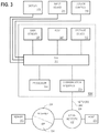
- Figure 3 is a block diagram that illustrates a computer system 300 upon which an embodiment of the invention may be implemented.
- Computer system 300 includes a bus 302 or other communication mechanism for communicating information, and a hardware processor 304 coupled with bus 302 for processing information.
- Hardware processor 304 may be, for example, a general purpose microprocessor.
- Computer system 300 also includes a main memory 306, such as a random access memory (RAM) or other dynamic storage device, coupled to bus 302 for storing information and instructions to be executed by processor 304.
- Main memory 306 also may be used for storing temporary variables or other intermediate information during execution of instructions to be executed by processor 304.
- Such instructions when stored in non-transitory storage media accessible to processor 304, render computer system 300 into a special-purpose machine that is customized to perform the operations specified in the instructions.
- Computer system 300 further includes a read only memory (ROM) 308 or other static storage device coupled to bus 302 for storing static information and instructions for processor 304.
- ROM read only memory
- a storage device 310 such as a magnetic disk or optical disk, is provided and coupled to bus 302 for storing information and instructions.
- Computer system 300 may be coupled via bus 302 to a display 312, such as a cathode ray tube (CRT), for displaying information to a computer user.
- a display 312 such as a cathode ray tube (CRT)
- cursor control 316 is Another type of user input device
- cursor control 316 such as a mouse, a trackball, or cursor direction keys for communicating direction information and command selections to processor 304 and for controlling cursor movement on display 312.
- This input device typically has two degrees of freedom in two axes, a first axis (e.g., x) and a second axis (e.g., y), that allows the device to specify positions in a plane.
- Computer system 300 may implement the techniques described herein using customized hard-wired logic, one or more ASICs or FPGAs, firmware and/or program logic which in combination with the computer system causes or programs computer system 300 to be a special-purpose machine. According to one embodiment, the techniques herein are performed by computer system 300 in response to processor 304 executing one or more sequences of one or more instructions contained in main memory 306. Such instructions may be read into main memory 306 from another storage medium, such as storage device 310. Execution of the sequences of instructions contained in main memory 306 causes processor 304 to perform the process steps described herein. In alternative embodiments, hard-wired circuitry may be used in place of or in combination with software instructions.
- Non-volatile media include, for example, optical or magnetic disks, such as storage device 310.
- Volatile media include dynamic memory, such as main memory 306.
- Common forms of storage media include, for example, a floppy disk, a flexible disk, hard disk, solid state drive, magnetic tape, or any other magnetic data storage medium, a CD-ROM, any other optical data storage medium, any physical medium with patterns of holes, a RAM, a PROM, and EPROM, a FLASH-EPROM, NVRAM, any other memory chip or cartridge, content-addressable memory (CAM), and ternary content-addressable memory (TCAM).
- a floppy disk a flexible disk, hard disk, solid state drive, magnetic tape, or any other magnetic data storage medium
- CD-ROM any other optical data storage medium
- any physical medium with patterns of holes a RAM, a PROM, and EPROM
- FLASH-EPROM any other memory chip or cartridge
- CAM content-addressable memory
- TCAM ternary content-addressable memory
- Storage media are distinct from but may be used in conjunction with transmission media.
- Transmission media participate in transferring information between storage media.
- transmission media include coaxial cables, copper wire and fiber optics, including the wires that comprise bus 302.
- transmission media can also take the form of acoustic or light waves, such as those generated during radio-wave and infra-red data communications.
- Various forms of media may be involved in carrying one or more sequences of one or more instructions to processor 304 for execution.
- the instructions may initially be carried on a magnetic disk or solid state drive of a remote computer.
- the remote computer can load the instructions into its dynamic memory and send the instructions over a telephone line using a modem.
- a modem local to computer system 300 can receive the data on the telephone line and use an infra-red transmitter to convert the data to an infra-red signal.
- An infra-red detector can receive the data carried in the infra-red signal and appropriate circuitry can place the data on bus 302.
- Bus 302 carries the data to main memory 306, from which processor 304 retrieves and executes the instructions.
- the instructions received by main memory 306 may optionally be stored on storage device 310 either before or after execution by processor 304.
- Computer system 300 also includes a communication interface 318 coupled to bus 302.
- Communication interface 318 provides a two-way data communication coupling to a network link 320 that is connected to a local network 322.
- communication interface 318 may be an integrated services digital network (ISDN) card, cable modem, satellite modem, or a modem to provide a data communication connection to a corresponding type of telephone line.
- ISDN integrated services digital network
- communication interface 318 may be a local area network (LAN) card to provide a data communication connection to a compatible LAN.
- LAN local area network
- Wireless links may also be implemented.
- communication interface 318 sends and receives electrical, electromagnetic or optical signals that carry digital data streams representing various types of information.
- Network link 320 typically provides data communication through one or more networks to other data devices.
- network link 320 may provide a connection through local network 322 to a host computer 324 or to data equipment operated by an Internet Service Provider (ISP) 326.
- ISP 326 in turn provides data communication services through the world wide packet data communication network now commonly referred to as the "Internet" 328.
- Internet 328 uses electrical, electromagnetic or optical signals that carry digital data streams.
- the signals through the various networks and the signals on network link 320 and through communication interface 318, which carry the digital data to and from computer system 300, are example forms of transmission media.
- Computer system 300 can send messages and receive data, including program code, through the network(s), network link 320 and communication interface 318.
- a server 330 might transmit a requested code for an application program through Internet 328, ISP 326, local network 322 and communication interface 318.
- the received code may be executed by processor 304 as it is received, and/or stored in storage device 310, or other non-volatile storage for later execution.
Landscapes
- Engineering & Computer Science (AREA)
- Theoretical Computer Science (AREA)
- Physics & Mathematics (AREA)
- General Engineering & Computer Science (AREA)
- General Physics & Mathematics (AREA)
- Human Computer Interaction (AREA)
- Computer Hardware Design (AREA)
- Computer Security & Cryptography (AREA)
- Software Systems (AREA)
- Mathematical Physics (AREA)
- Storage Device Security (AREA)
- Microcomputers (AREA)
- Logic Circuits (AREA)
Applications Claiming Priority (2)
| Application Number | Priority Date | Filing Date | Title |
|---|---|---|---|
| US15/466,484 US10585608B2 (en) | 2017-03-22 | 2017-03-22 | System and method for securely isolating a system feature |
| PCT/US2017/064824 WO2018174971A1 (en) | 2017-03-22 | 2017-12-06 | System and method for securely isolating a system feature |
Publications (2)
| Publication Number | Publication Date |
|---|---|
| EP3602390A1 EP3602390A1 (en) | 2020-02-05 |
| EP3602390B1 true EP3602390B1 (en) | 2021-11-17 |
Family
ID=60782386
Family Applications (1)
| Application Number | Title | Priority Date | Filing Date |
|---|---|---|---|
| EP17818398.4A Active EP3602390B1 (en) | 2017-03-22 | 2017-12-06 | System and method for securely isolating a system feature |
Country Status (5)
| Country | Link |
|---|---|
| US (1) | US10585608B2 (ja) |
| EP (1) | EP3602390B1 (ja) |
| JP (2) | JP7159190B2 (ja) |
| CN (1) | CN110462624B (ja) |
| WO (1) | WO2018174971A1 (ja) |
Families Citing this family (1)
| Publication number | Priority date | Publication date | Assignee | Title |
|---|---|---|---|---|
| US11099922B2 (en) * | 2019-08-12 | 2021-08-24 | Dell Products L.P. | System and method for isolating a failed card |
Family Cites Families (19)
| Publication number | Priority date | Publication date | Assignee | Title |
|---|---|---|---|---|
| US5524008A (en) * | 1995-03-21 | 1996-06-04 | National Semiconductor Corporation | Generating real-time events in a TDMA digital wireless communications system |
| JP2000267847A (ja) | 1999-03-18 | 2000-09-29 | Miyazaki Oki Electric Co Ltd | セキュリティシステム |
| US7149854B2 (en) * | 2001-05-10 | 2006-12-12 | Advanced Micro Devices, Inc. | External locking mechanism for personal computer memory locations |
| JP4256859B2 (ja) * | 2005-04-21 | 2009-04-22 | シャープ株式会社 | 半導体記憶装置 |
| US20080005462A1 (en) * | 2006-06-30 | 2008-01-03 | Mosaid Technologies Incorporated | Method of configuring non-volatile memory for a hybrid disk drive |
| US7594144B2 (en) * | 2006-08-14 | 2009-09-22 | International Business Machines Corporation | Handling fatal computer hardware errors |
| KR100833189B1 (ko) * | 2006-11-03 | 2008-05-28 | 삼성전자주식회사 | 불휘발성 메모리 장치 및 불휘발성 메모리 장치의환경설정정보 설정 방법 |
| US7574576B2 (en) * | 2006-12-22 | 2009-08-11 | Spansion Llc | Semiconductor device and method of controlling the same |
| US7902964B2 (en) | 2007-06-05 | 2011-03-08 | Xerox Corporation | Hybrid system option key |
| US8392683B1 (en) * | 2009-11-30 | 2013-03-05 | Micron Technology, Inc. | Dynamic range unlock or lock memory device and method to operate the same |
| US10771448B2 (en) * | 2012-08-10 | 2020-09-08 | Cryptography Research, Inc. | Secure feature and key management in integrated circuits |
| US9521032B1 (en) * | 2013-03-14 | 2016-12-13 | Amazon Technologies, Inc. | Server for authentication, authorization, and accounting |
| US20140359196A1 (en) * | 2013-05-31 | 2014-12-04 | Daniel J. Ragland | On-the-fly performance adjustment for solid state storage devices |
| US9940048B2 (en) * | 2014-02-26 | 2018-04-10 | Macronix International Co., Ltd. | Nonvolatile memory data protection using nonvolatile protection codes and volatile protection codes |
| US20150381368A1 (en) * | 2014-06-27 | 2015-12-31 | William A. Stevens, Jr. | Technologies for secure offline activation of hardware features |
| US9747739B2 (en) * | 2014-08-18 | 2017-08-29 | Noke, Inc. | Wireless locking device |
| KR102407066B1 (ko) * | 2014-09-17 | 2022-06-08 | 크라이프토그라피 리서치, 인코포레이티드 | 집적 회로를 위한 상이한 엔티티들의 특권들의 관리 |
| JP6492835B2 (ja) * | 2015-03-23 | 2019-04-03 | 富士通クライアントコンピューティング株式会社 | ポータブル機器、及び情報処理装置 |
| CN106227636A (zh) * | 2016-07-20 | 2016-12-14 | 国网安徽省电力公司信息通信分公司 | 一种基于ipmi的数据中心带外管理系统 |
-
2017
- 2017-03-22 US US15/466,484 patent/US10585608B2/en active Active
- 2017-12-06 WO PCT/US2017/064824 patent/WO2018174971A1/en active Search and Examination
- 2017-12-06 JP JP2019552241A patent/JP7159190B2/ja active Active
- 2017-12-06 EP EP17818398.4A patent/EP3602390B1/en active Active
- 2017-12-06 CN CN201780088688.5A patent/CN110462624B/zh active Active
-
2022
- 2022-07-22 JP JP2022117179A patent/JP7441896B2/ja active Active
Also Published As
| Publication number | Publication date |
|---|---|
| JP2020514927A (ja) | 2020-05-21 |
| CN110462624A (zh) | 2019-11-15 |
| JP7159190B2 (ja) | 2022-10-24 |
| CN110462624B (zh) | 2023-08-29 |
| WO2018174971A1 (en) | 2018-09-27 |
| JP2022141880A (ja) | 2022-09-29 |
| JP7441896B2 (ja) | 2024-03-01 |
| US20180275904A1 (en) | 2018-09-27 |
| EP3602390A1 (en) | 2020-02-05 |
| US10585608B2 (en) | 2020-03-10 |
Similar Documents
| Publication | Publication Date | Title |
|---|---|---|
| EP3602374B1 (en) | System and method for restoration of a trusted system firmware state | |
| US8566603B2 (en) | Managing security operating modes | |
| US10769089B1 (en) | Combination write blocking systems with connection interface control devices and methods | |
| CN103262092B (zh) | 基于存储驱动器的防恶意软件方法和装置 | |
| US7210014B2 (en) | Alternative methods in memory protection | |
| US20080104348A1 (en) | Security System And Method For Computer Operating Systems | |
| US20070011419A1 (en) | Method and system for a multi-sharing security firewall | |
| US20110307639A1 (en) | Virtual serial port management system and method | |
| US10089248B2 (en) | Hacking-resistant computer design | |
| US10387646B2 (en) | Input/output parameter selection | |
| US20170201373A1 (en) | Systems and methods for management controller management of key encryption key | |
| Kataria et al. | Defeating cisco trust anchor: A {Case-Study} of recent advancements in direct {FPGA} bitstream manipulation | |
| JP7441896B2 (ja) | システム特徴をセキュアに分離するためのシステムおよび方法 | |
| US20230315463A1 (en) | Methods and devices for defeating buffer overflow problems in multi-core processors | |
| EP4258146A1 (en) | Computer system, trusted functional assembly, and operation method | |
| US11734457B2 (en) | Technology for controlling access to processor debug features | |
| CN105550567A (zh) | 一种Windows虚拟机USB设备读写权限管控方法 | |
| CN110334501A (zh) | 一种基于u盘的数据保护方法和装置以及设备 | |
| EP3583538A1 (en) | Hacking-resistant computer design | |
| EP4217889A1 (en) | Secure collection and communication of computing device working data |
Legal Events
| Date | Code | Title | Description |
|---|---|---|---|
| STAA | Information on the status of an ep patent application or granted ep patent |
Free format text: STATUS: UNKNOWN |
|
| STAA | Information on the status of an ep patent application or granted ep patent |
Free format text: STATUS: THE INTERNATIONAL PUBLICATION HAS BEEN MADE |
|
| PUAI | Public reference made under article 153(3) epc to a published international application that has entered the european phase |
Free format text: ORIGINAL CODE: 0009012 |
|
| STAA | Information on the status of an ep patent application or granted ep patent |
Free format text: STATUS: REQUEST FOR EXAMINATION WAS MADE |
|
| 17P | Request for examination filed |
Effective date: 20191017 |
|
| AK | Designated contracting states |
Kind code of ref document: A1 Designated state(s): AL AT BE BG CH CY CZ DE DK EE ES FI FR GB GR HR HU IE IS IT LI LT LU LV MC MK MT NL NO PL PT RO RS SE SI SK SM TR |
|
| AX | Request for extension of the european patent |
Extension state: BA ME |
|
| DAV | Request for validation of the european patent (deleted) | ||
| DAX | Request for extension of the european patent (deleted) | ||
| STAA | Information on the status of an ep patent application or granted ep patent |
Free format text: STATUS: EXAMINATION IS IN PROGRESS |
|
| 17Q | First examination report despatched |
Effective date: 20210303 |
|
| GRAP | Despatch of communication of intention to grant a patent |
Free format text: ORIGINAL CODE: EPIDOSNIGR1 |
|
| STAA | Information on the status of an ep patent application or granted ep patent |
Free format text: STATUS: GRANT OF PATENT IS INTENDED |
|
| INTG | Intention to grant announced |
Effective date: 20210607 |
|
| GRAS | Grant fee paid |
Free format text: ORIGINAL CODE: EPIDOSNIGR3 |
|
| GRAA | (expected) grant |
Free format text: ORIGINAL CODE: 0009210 |
|
| STAA | Information on the status of an ep patent application or granted ep patent |
Free format text: STATUS: THE PATENT HAS BEEN GRANTED |
|
| AK | Designated contracting states |
Kind code of ref document: B1 Designated state(s): AL AT BE BG CH CY CZ DE DK EE ES FI FR GB GR HR HU IE IS IT LI LT LU LV MC MK MT NL NO PL PT RO RS SE SI SK SM TR |
|
| REG | Reference to a national code |
Ref country code: GB Ref legal event code: FG4D |
|
| REG | Reference to a national code |
Ref country code: DE Ref legal event code: R096 Ref document number: 602017049546 Country of ref document: DE |
|
| REG | Reference to a national code |
Ref country code: IE Ref legal event code: FG4D |
|
| REG | Reference to a national code |
Ref country code: AT Ref legal event code: REF Ref document number: 1448682 Country of ref document: AT Kind code of ref document: T Effective date: 20211215 |
|
| REG | Reference to a national code |
Ref country code: LT Ref legal event code: MG9D |
|
| REG | Reference to a national code |
Ref country code: NL Ref legal event code: MP Effective date: 20211117 |
|
| REG | Reference to a national code |
Ref country code: AT Ref legal event code: MK05 Ref document number: 1448682 Country of ref document: AT Kind code of ref document: T Effective date: 20211117 |
|
| PG25 | Lapsed in a contracting state [announced via postgrant information from national office to epo] |
Ref country code: RS Free format text: LAPSE BECAUSE OF FAILURE TO SUBMIT A TRANSLATION OF THE DESCRIPTION OR TO PAY THE FEE WITHIN THE PRESCRIBED TIME-LIMIT Effective date: 20211117 Ref country code: LT Free format text: LAPSE BECAUSE OF FAILURE TO SUBMIT A TRANSLATION OF THE DESCRIPTION OR TO PAY THE FEE WITHIN THE PRESCRIBED TIME-LIMIT Effective date: 20211117 Ref country code: FI Free format text: LAPSE BECAUSE OF FAILURE TO SUBMIT A TRANSLATION OF THE DESCRIPTION OR TO PAY THE FEE WITHIN THE PRESCRIBED TIME-LIMIT Effective date: 20211117 Ref country code: BG Free format text: LAPSE BECAUSE OF FAILURE TO SUBMIT A TRANSLATION OF THE DESCRIPTION OR TO PAY THE FEE WITHIN THE PRESCRIBED TIME-LIMIT Effective date: 20220217 Ref country code: AT Free format text: LAPSE BECAUSE OF FAILURE TO SUBMIT A TRANSLATION OF THE DESCRIPTION OR TO PAY THE FEE WITHIN THE PRESCRIBED TIME-LIMIT Effective date: 20211117 |
|
| PG25 | Lapsed in a contracting state [announced via postgrant information from national office to epo] |
Ref country code: IS Free format text: LAPSE BECAUSE OF FAILURE TO SUBMIT A TRANSLATION OF THE DESCRIPTION OR TO PAY THE FEE WITHIN THE PRESCRIBED TIME-LIMIT Effective date: 20220317 Ref country code: SE Free format text: LAPSE BECAUSE OF FAILURE TO SUBMIT A TRANSLATION OF THE DESCRIPTION OR TO PAY THE FEE WITHIN THE PRESCRIBED TIME-LIMIT Effective date: 20211117 Ref country code: PT Free format text: LAPSE BECAUSE OF FAILURE TO SUBMIT A TRANSLATION OF THE DESCRIPTION OR TO PAY THE FEE WITHIN THE PRESCRIBED TIME-LIMIT Effective date: 20220317 Ref country code: PL Free format text: LAPSE BECAUSE OF FAILURE TO SUBMIT A TRANSLATION OF THE DESCRIPTION OR TO PAY THE FEE WITHIN THE PRESCRIBED TIME-LIMIT Effective date: 20211117 Ref country code: NO Free format text: LAPSE BECAUSE OF FAILURE TO SUBMIT A TRANSLATION OF THE DESCRIPTION OR TO PAY THE FEE WITHIN THE PRESCRIBED TIME-LIMIT Effective date: 20220217 Ref country code: NL Free format text: LAPSE BECAUSE OF FAILURE TO SUBMIT A TRANSLATION OF THE DESCRIPTION OR TO PAY THE FEE WITHIN THE PRESCRIBED TIME-LIMIT Effective date: 20211117 Ref country code: LV Free format text: LAPSE BECAUSE OF FAILURE TO SUBMIT A TRANSLATION OF THE DESCRIPTION OR TO PAY THE FEE WITHIN THE PRESCRIBED TIME-LIMIT Effective date: 20211117 Ref country code: HR Free format text: LAPSE BECAUSE OF FAILURE TO SUBMIT A TRANSLATION OF THE DESCRIPTION OR TO PAY THE FEE WITHIN THE PRESCRIBED TIME-LIMIT Effective date: 20211117 Ref country code: GR Free format text: LAPSE BECAUSE OF FAILURE TO SUBMIT A TRANSLATION OF THE DESCRIPTION OR TO PAY THE FEE WITHIN THE PRESCRIBED TIME-LIMIT Effective date: 20220218 Ref country code: ES Free format text: LAPSE BECAUSE OF FAILURE TO SUBMIT A TRANSLATION OF THE DESCRIPTION OR TO PAY THE FEE WITHIN THE PRESCRIBED TIME-LIMIT Effective date: 20211117 |
|
| PG25 | Lapsed in a contracting state [announced via postgrant information from national office to epo] |
Ref country code: SM Free format text: LAPSE BECAUSE OF FAILURE TO SUBMIT A TRANSLATION OF THE DESCRIPTION OR TO PAY THE FEE WITHIN THE PRESCRIBED TIME-LIMIT Effective date: 20211117 Ref country code: SK Free format text: LAPSE BECAUSE OF FAILURE TO SUBMIT A TRANSLATION OF THE DESCRIPTION OR TO PAY THE FEE WITHIN THE PRESCRIBED TIME-LIMIT Effective date: 20211117 Ref country code: RO Free format text: LAPSE BECAUSE OF FAILURE TO SUBMIT A TRANSLATION OF THE DESCRIPTION OR TO PAY THE FEE WITHIN THE PRESCRIBED TIME-LIMIT Effective date: 20211117 Ref country code: EE Free format text: LAPSE BECAUSE OF FAILURE TO SUBMIT A TRANSLATION OF THE DESCRIPTION OR TO PAY THE FEE WITHIN THE PRESCRIBED TIME-LIMIT Effective date: 20211117 Ref country code: DK Free format text: LAPSE BECAUSE OF FAILURE TO SUBMIT A TRANSLATION OF THE DESCRIPTION OR TO PAY THE FEE WITHIN THE PRESCRIBED TIME-LIMIT Effective date: 20211117 Ref country code: CZ Free format text: LAPSE BECAUSE OF FAILURE TO SUBMIT A TRANSLATION OF THE DESCRIPTION OR TO PAY THE FEE WITHIN THE PRESCRIBED TIME-LIMIT Effective date: 20211117 |
|
| REG | Reference to a national code |
Ref country code: CH Ref legal event code: PL |
|
| REG | Reference to a national code |
Ref country code: DE Ref legal event code: R097 Ref document number: 602017049546 Country of ref document: DE |
|
| PG25 | Lapsed in a contracting state [announced via postgrant information from national office to epo] |
Ref country code: MC Free format text: LAPSE BECAUSE OF FAILURE TO SUBMIT A TRANSLATION OF THE DESCRIPTION OR TO PAY THE FEE WITHIN THE PRESCRIBED TIME-LIMIT Effective date: 20211117 |
|
| PLBE | No opposition filed within time limit |
Free format text: ORIGINAL CODE: 0009261 |
|
| STAA | Information on the status of an ep patent application or granted ep patent |
Free format text: STATUS: NO OPPOSITION FILED WITHIN TIME LIMIT |
|
| REG | Reference to a national code |
Ref country code: BE Ref legal event code: MM Effective date: 20211231 |
|
| 26N | No opposition filed |
Effective date: 20220818 |
|
| PG25 | Lapsed in a contracting state [announced via postgrant information from national office to epo] |
Ref country code: LU Free format text: LAPSE BECAUSE OF NON-PAYMENT OF DUE FEES Effective date: 20211206 Ref country code: IE Free format text: LAPSE BECAUSE OF NON-PAYMENT OF DUE FEES Effective date: 20211206 Ref country code: AL Free format text: LAPSE BECAUSE OF FAILURE TO SUBMIT A TRANSLATION OF THE DESCRIPTION OR TO PAY THE FEE WITHIN THE PRESCRIBED TIME-LIMIT Effective date: 20211117 |
|
| PG25 | Lapsed in a contracting state [announced via postgrant information from national office to epo] |
Ref country code: SI Free format text: LAPSE BECAUSE OF FAILURE TO SUBMIT A TRANSLATION OF THE DESCRIPTION OR TO PAY THE FEE WITHIN THE PRESCRIBED TIME-LIMIT Effective date: 20211117 Ref country code: FR Free format text: LAPSE BECAUSE OF NON-PAYMENT OF DUE FEES Effective date: 20220117 Ref country code: BE Free format text: LAPSE BECAUSE OF NON-PAYMENT OF DUE FEES Effective date: 20211231 |
|
| PG25 | Lapsed in a contracting state [announced via postgrant information from national office to epo] |
Ref country code: LI Free format text: LAPSE BECAUSE OF NON-PAYMENT OF DUE FEES Effective date: 20211231 Ref country code: CH Free format text: LAPSE BECAUSE OF NON-PAYMENT OF DUE FEES Effective date: 20211231 |
|
| PG25 | Lapsed in a contracting state [announced via postgrant information from national office to epo] |
Ref country code: IT Free format text: LAPSE BECAUSE OF FAILURE TO SUBMIT A TRANSLATION OF THE DESCRIPTION OR TO PAY THE FEE WITHIN THE PRESCRIBED TIME-LIMIT Effective date: 20211117 |
|
| PG25 | Lapsed in a contracting state [announced via postgrant information from national office to epo] |
Ref country code: CY Free format text: LAPSE BECAUSE OF FAILURE TO SUBMIT A TRANSLATION OF THE DESCRIPTION OR TO PAY THE FEE WITHIN THE PRESCRIBED TIME-LIMIT Effective date: 20211117 |
|
| P01 | Opt-out of the competence of the unified patent court (upc) registered |
Effective date: 20230526 |
|
| PG25 | Lapsed in a contracting state [announced via postgrant information from national office to epo] |
Ref country code: HU Free format text: LAPSE BECAUSE OF FAILURE TO SUBMIT A TRANSLATION OF THE DESCRIPTION OR TO PAY THE FEE WITHIN THE PRESCRIBED TIME-LIMIT; INVALID AB INITIO Effective date: 20171206 |
|
| PGFP | Annual fee paid to national office [announced via postgrant information from national office to epo] |
Ref country code: GB Payment date: 20231102 Year of fee payment: 7 |
|
| PGFP | Annual fee paid to national office [announced via postgrant information from national office to epo] |
Ref country code: DE Payment date: 20231031 Year of fee payment: 7 |
|
| PG25 | Lapsed in a contracting state [announced via postgrant information from national office to epo] |
Ref country code: MK Free format text: LAPSE BECAUSE OF FAILURE TO SUBMIT A TRANSLATION OF THE DESCRIPTION OR TO PAY THE FEE WITHIN THE PRESCRIBED TIME-LIMIT Effective date: 20211117 |