JP7151907B2 - Capacitor and manufacturing method thereof - Google Patents
Capacitor and manufacturing method thereof Download PDFInfo
- Publication number
- JP7151907B2 JP7151907B2 JP2021548315A JP2021548315A JP7151907B2 JP 7151907 B2 JP7151907 B2 JP 7151907B2 JP 2021548315 A JP2021548315 A JP 2021548315A JP 2021548315 A JP2021548315 A JP 2021548315A JP 7151907 B2 JP7151907 B2 JP 7151907B2
- Authority
- JP
- Japan
- Prior art keywords
- conductive
- columnar portions
- dielectric layer
- capacitor
- support portion
- Prior art date
- Legal status (The legal status is an assumption and is not a legal conclusion. Google has not performed a legal analysis and makes no representation as to the accuracy of the status listed.)
- Active
Links
- 239000003990 capacitor Substances 0.000 title claims description 199
- 238000004519 manufacturing process Methods 0.000 title claims description 41
- 239000000853 adhesive Substances 0.000 claims description 58
- 230000001070 adhesive effect Effects 0.000 claims description 58
- 238000000034 method Methods 0.000 claims description 36
- OKTJSMMVPCPJKN-UHFFFAOYSA-N Carbon Chemical compound [C] OKTJSMMVPCPJKN-UHFFFAOYSA-N 0.000 claims description 27
- 239000002041 carbon nanotube Substances 0.000 claims description 25
- 229910021393 carbon nanotube Inorganic materials 0.000 claims description 25
- 239000002105 nanoparticle Substances 0.000 claims description 15
- 229910052751 metal Inorganic materials 0.000 claims description 12
- 239000002184 metal Substances 0.000 claims description 12
- 239000007788 liquid Substances 0.000 claims description 4
- 238000010030 laminating Methods 0.000 claims description 2
- 238000003825 pressing Methods 0.000 claims description 2
- 239000004020 conductor Substances 0.000 description 32
- 239000000463 material Substances 0.000 description 19
- 238000000576 coating method Methods 0.000 description 13
- 239000011248 coating agent Substances 0.000 description 12
- 238000005229 chemical vapour deposition Methods 0.000 description 9
- 238000012986 modification Methods 0.000 description 9
- 230000004048 modification Effects 0.000 description 9
- 239000003054 catalyst Substances 0.000 description 6
- 239000002245 particle Substances 0.000 description 6
- 238000000231 atomic layer deposition Methods 0.000 description 5
- 239000000758 substrate Substances 0.000 description 5
- 238000010586 diagram Methods 0.000 description 4
- 239000012530 fluid Substances 0.000 description 4
- 239000007789 gas Substances 0.000 description 4
- 239000011810 insulating material Substances 0.000 description 4
- VNWKTOKETHGBQD-UHFFFAOYSA-N methane Chemical compound C VNWKTOKETHGBQD-UHFFFAOYSA-N 0.000 description 4
- VYPSYNLAJGMNEJ-UHFFFAOYSA-N Silicium dioxide Chemical compound O=[Si]=O VYPSYNLAJGMNEJ-UHFFFAOYSA-N 0.000 description 3
- 229910045601 alloy Inorganic materials 0.000 description 3
- 239000000956 alloy Substances 0.000 description 3
- 229910052782 aluminium Inorganic materials 0.000 description 3
- XAGFODPZIPBFFR-UHFFFAOYSA-N aluminium Chemical compound [Al] XAGFODPZIPBFFR-UHFFFAOYSA-N 0.000 description 3
- 239000002131 composite material Substances 0.000 description 3
- 238000000151 deposition Methods 0.000 description 3
- 230000008021 deposition Effects 0.000 description 3
- 238000003475 lamination Methods 0.000 description 3
- 238000000623 plasma-assisted chemical vapour deposition Methods 0.000 description 3
- BASFCYQUMIYNBI-UHFFFAOYSA-N platinum Substances [Pt] BASFCYQUMIYNBI-UHFFFAOYSA-N 0.000 description 3
- 239000004065 semiconductor Substances 0.000 description 3
- 238000004544 sputter deposition Methods 0.000 description 3
- QGZKDVFQNNGYKY-UHFFFAOYSA-N Ammonia Chemical compound N QGZKDVFQNNGYKY-UHFFFAOYSA-N 0.000 description 2
- RYGMFSIKBFXOCR-UHFFFAOYSA-N Copper Chemical compound [Cu] RYGMFSIKBFXOCR-UHFFFAOYSA-N 0.000 description 2
- 239000002134 carbon nanofiber Substances 0.000 description 2
- 229910052802 copper Inorganic materials 0.000 description 2
- 239000010949 copper Substances 0.000 description 2
- 239000000945 filler Substances 0.000 description 2
- 229910052737 gold Inorganic materials 0.000 description 2
- 239000010931 gold Substances 0.000 description 2
- 239000002048 multi walled nanotube Substances 0.000 description 2
- 239000002121 nanofiber Substances 0.000 description 2
- 230000003071 parasitic effect Effects 0.000 description 2
- 238000005240 physical vapour deposition Methods 0.000 description 2
- 238000007747 plating Methods 0.000 description 2
- 229910052697 platinum Inorganic materials 0.000 description 2
- 239000002109 single walled nanotube Substances 0.000 description 2
- 239000011787 zinc oxide Substances 0.000 description 2
- OEPOKWHJYJXUGD-UHFFFAOYSA-N 2-(3-phenylmethoxyphenyl)-1,3-thiazole-4-carbaldehyde Chemical compound O=CC1=CSC(C=2C=C(OCC=3C=CC=CC=3)C=CC=2)=N1 OEPOKWHJYJXUGD-UHFFFAOYSA-N 0.000 description 1
- JBRZTFJDHDCESZ-UHFFFAOYSA-N AsGa Chemical compound [As]#[Ga] JBRZTFJDHDCESZ-UHFFFAOYSA-N 0.000 description 1
- UGFAIRIUMAVXCW-UHFFFAOYSA-N Carbon monoxide Chemical compound [O+]#[C-] UGFAIRIUMAVXCW-UHFFFAOYSA-N 0.000 description 1
- VGGSQFUCUMXWEO-UHFFFAOYSA-N Ethene Chemical compound C=C VGGSQFUCUMXWEO-UHFFFAOYSA-N 0.000 description 1
- 239000005977 Ethylene Substances 0.000 description 1
- 229910001218 Gallium arsenide Inorganic materials 0.000 description 1
- UFHFLCQGNIYNRP-UHFFFAOYSA-N Hydrogen Chemical compound [H][H] UFHFLCQGNIYNRP-UHFFFAOYSA-N 0.000 description 1
- 239000002033 PVDF binder Substances 0.000 description 1
- 229910052581 Si3N4 Inorganic materials 0.000 description 1
- XUIMIQQOPSSXEZ-UHFFFAOYSA-N Silicon Chemical compound [Si] XUIMIQQOPSSXEZ-UHFFFAOYSA-N 0.000 description 1
- BQCADISMDOOEFD-UHFFFAOYSA-N Silver Chemical compound [Ag] BQCADISMDOOEFD-UHFFFAOYSA-N 0.000 description 1
- HSFWRNGVRCDJHI-UHFFFAOYSA-N alpha-acetylene Natural products C#C HSFWRNGVRCDJHI-UHFFFAOYSA-N 0.000 description 1
- 229910021529 ammonia Inorganic materials 0.000 description 1
- 229910002113 barium titanate Inorganic materials 0.000 description 1
- JRPBQTZRNDNNOP-UHFFFAOYSA-N barium titanate Chemical compound [Ba+2].[Ba+2].[O-][Ti]([O-])([O-])[O-] JRPBQTZRNDNNOP-UHFFFAOYSA-N 0.000 description 1
- 230000015572 biosynthetic process Effects 0.000 description 1
- 229910002091 carbon monoxide Inorganic materials 0.000 description 1
- 239000000919 ceramic Substances 0.000 description 1
- 238000003486 chemical etching Methods 0.000 description 1
- 239000003795 chemical substances by application Substances 0.000 description 1
- 229920001940 conductive polymer Polymers 0.000 description 1
- 238000001035 drying Methods 0.000 description 1
- 230000000694 effects Effects 0.000 description 1
- 238000005530 etching Methods 0.000 description 1
- 125000002534 ethynyl group Chemical group [H]C#C* 0.000 description 1
- PCHJSUWPFVWCPO-UHFFFAOYSA-N gold Chemical compound [Au] PCHJSUWPFVWCPO-UHFFFAOYSA-N 0.000 description 1
- 229910000449 hafnium oxide Inorganic materials 0.000 description 1
- WIHZLLGSGQNAGK-UHFFFAOYSA-N hafnium(4+);oxygen(2-) Chemical compound [O-2].[O-2].[Hf+4] WIHZLLGSGQNAGK-UHFFFAOYSA-N 0.000 description 1
- 238000010438 heat treatment Methods 0.000 description 1
- 229910052595 hematite Inorganic materials 0.000 description 1
- 239000011019 hematite Substances 0.000 description 1
- 229910052739 hydrogen Inorganic materials 0.000 description 1
- 239000001257 hydrogen Substances 0.000 description 1
- 238000003780 insertion Methods 0.000 description 1
- 230000037431 insertion Effects 0.000 description 1
- 229910052742 iron Inorganic materials 0.000 description 1
- LIKBJVNGSGBSGK-UHFFFAOYSA-N iron(3+);oxygen(2-) Chemical compound [O-2].[O-2].[O-2].[Fe+3].[Fe+3] LIKBJVNGSGBSGK-UHFFFAOYSA-N 0.000 description 1
- HFGPZNIAWCZYJU-UHFFFAOYSA-N lead zirconate titanate Chemical compound [O-2].[O-2].[O-2].[O-2].[O-2].[Ti+4].[Zr+4].[Pb+2] HFGPZNIAWCZYJU-UHFFFAOYSA-N 0.000 description 1
- 229910052451 lead zirconate titanate Inorganic materials 0.000 description 1
- 238000001459 lithography Methods 0.000 description 1
- 239000000203 mixture Substances 0.000 description 1
- 239000002073 nanorod Substances 0.000 description 1
- 239000002070 nanowire Substances 0.000 description 1
- 229910052759 nickel Inorganic materials 0.000 description 1
- TWNQGVIAIRXVLR-UHFFFAOYSA-N oxo(oxoalumanyloxy)alumane Chemical compound O=[Al]O[Al]=O TWNQGVIAIRXVLR-UHFFFAOYSA-N 0.000 description 1
- BPUBBGLMJRNUCC-UHFFFAOYSA-N oxygen(2-);tantalum(5+) Chemical compound [O-2].[O-2].[O-2].[O-2].[O-2].[Ta+5].[Ta+5] BPUBBGLMJRNUCC-UHFFFAOYSA-N 0.000 description 1
- 238000000059 patterning Methods 0.000 description 1
- 230000000149 penetrating effect Effects 0.000 description 1
- 239000002861 polymer material Substances 0.000 description 1
- 229920002981 polyvinylidene fluoride Polymers 0.000 description 1
- 239000011347 resin Substances 0.000 description 1
- 229920005989 resin Polymers 0.000 description 1
- 238000000926 separation method Methods 0.000 description 1
- 229910052710 silicon Inorganic materials 0.000 description 1
- 239000010703 silicon Substances 0.000 description 1
- 235000012239 silicon dioxide Nutrition 0.000 description 1
- 239000000377 silicon dioxide Substances 0.000 description 1
- HQVNEWCFYHHQES-UHFFFAOYSA-N silicon nitride Chemical compound N12[Si]34N5[Si]62N3[Si]51N64 HQVNEWCFYHHQES-UHFFFAOYSA-N 0.000 description 1
- 229910052814 silicon oxide Inorganic materials 0.000 description 1
- 229910052709 silver Inorganic materials 0.000 description 1
- 239000004332 silver Substances 0.000 description 1
- 229910001936 tantalum oxide Inorganic materials 0.000 description 1
Images


Classifications
-
- H—ELECTRICITY
- H01—ELECTRIC ELEMENTS
- H01G—CAPACITORS; CAPACITORS, RECTIFIERS, DETECTORS, SWITCHING DEVICES OR LIGHT-SENSITIVE DEVICES, OF THE ELECTROLYTIC TYPE
- H01G4/00—Fixed capacitors; Processes of their manufacture
- H01G4/30—Stacked capacitors
-
- H—ELECTRICITY
- H01—ELECTRIC ELEMENTS
- H01G—CAPACITORS; CAPACITORS, RECTIFIERS, DETECTORS, SWITCHING DEVICES OR LIGHT-SENSITIVE DEVICES, OF THE ELECTROLYTIC TYPE
- H01G4/00—Fixed capacitors; Processes of their manufacture
- H01G4/33—Thin- or thick-film capacitors
-
- H—ELECTRICITY
- H01—ELECTRIC ELEMENTS
- H01G—CAPACITORS; CAPACITORS, RECTIFIERS, DETECTORS, SWITCHING DEVICES OR LIGHT-SENSITIVE DEVICES, OF THE ELECTROLYTIC TYPE
- H01G4/00—Fixed capacitors; Processes of their manufacture
- H01G4/002—Details
- H01G4/005—Electrodes
-
- H—ELECTRICITY
- H01—ELECTRIC ELEMENTS
- H01G—CAPACITORS; CAPACITORS, RECTIFIERS, DETECTORS, SWITCHING DEVICES OR LIGHT-SENSITIVE DEVICES, OF THE ELECTROLYTIC TYPE
- H01G4/00—Fixed capacitors; Processes of their manufacture
- H01G4/002—Details
- H01G4/018—Dielectrics
- H01G4/06—Solid dielectrics
-
- H—ELECTRICITY
- H01—ELECTRIC ELEMENTS
- H01G—CAPACITORS; CAPACITORS, RECTIFIERS, DETECTORS, SWITCHING DEVICES OR LIGHT-SENSITIVE DEVICES, OF THE ELECTROLYTIC TYPE
- H01G4/00—Fixed capacitors; Processes of their manufacture
- H01G4/002—Details
- H01G4/018—Dielectrics
- H01G4/06—Solid dielectrics
- H01G4/08—Inorganic dielectrics
-
- H—ELECTRICITY
- H01—ELECTRIC ELEMENTS
- H01G—CAPACITORS; CAPACITORS, RECTIFIERS, DETECTORS, SWITCHING DEVICES OR LIGHT-SENSITIVE DEVICES, OF THE ELECTROLYTIC TYPE
- H01G4/00—Fixed capacitors; Processes of their manufacture
- H01G4/38—Multiple capacitors, i.e. structural combinations of fixed capacitors
Description
本発明は、キャパシタおよびその製造方法に関する。 The present invention relates to a capacitor and its manufacturing method.
キャパシタの構成を開示した文献として、特開2005-129566号公報(特許文献1)と特許第5091242号公報(特許文献2)とがある。特許文献1に記載されたキャパシタは、正電極と、負電極と、正電極および負電極の各極に設けられたカーボンナノチューブと、正電極および負電極の間においてカーボンナノチューブ間に充填されたポリフッ化ビニリデン(PVDF誘電体)と、を備えている。正電極および負電極は互いに対向している。正電極および負電極の一方に設けられたカーボンナノチューブは、他方に設けられたカーボンナノチューブ間に介挿されている。 Japanese Patent Application Laid-Open No. 2005-129566 (Patent Document 1) and Japanese Patent No. 5091242 (Patent Document 2) are documents that disclose the configuration of the capacitor. The capacitor described in Patent Document 1 includes a positive electrode, a negative electrode, carbon nanotubes provided at each of the positive electrode and the negative electrode, and polyfluoride filled between the carbon nanotubes between the positive electrode and the negative electrode. vinylidene chloride (PVDF dielectric); The positive and negative electrodes face each other. The carbon nanotubes provided on one of the positive and negative electrodes are interposed between the carbon nanotubes provided on the other.
特許文献2に記載されたキャパシタは、3D MIMキャパシタであって、下部プレートおよび上部プレートを備えている。下部プレートは、導電材料の層で形成されている。上部プレートも、導電材料の層で形成されている。上部プレートおよび下部プレートの各々は、高誘電率材料で形成された絶縁層によって分離されている。これらの層は、多数のナノファイバーが成長している表面をコーティング(被覆)している。 The capacitor described in US Pat. No. 6,200,000 is a 3D MIM capacitor with a bottom plate and a top plate. The bottom plate is formed of a layer of conductive material. The top plate is also formed of a layer of conductive material. Each of the upper and lower plates is separated by an insulating layer formed of a high dielectric constant material. These layers coat the surface on which numerous nanofibers are grown.
カーボンナノチューブまたはナノファイバーなどの、ナノサイズの外径を有する導電柱状部を備えるキャパシタ、たとえば、特許文献1に記載されたキャパシタの耐電圧を向上させるためには、互いに同一の2つのキャパシタを積層させることで複合キャパシタを形成することが考えられる。しかしながら、複合キャパシタは、積層前の1つのキャパシタに対して、体積が2倍となり、静電容量は半分となる。すなわち、上記のような複合キャパシタは、積層前の1つのキャパシタに対して、体積容量密度が4分の1となる。 In order to improve the withstand voltage of a capacitor with a conductive columnar part having a nano-sized outer diameter, such as a carbon nanotube or nanofiber, for example, the capacitor described in Patent Document 1, two capacitors identical to each other are stacked. It is conceivable to form a composite capacitor by However, the composite capacitor has twice the volume and half the capacitance of a single capacitor before lamination. That is, the composite capacitor as described above has a volumetric capacity density of 1/4 that of a single capacitor before lamination.
また、たとえば、特許文献2に記載されたキャパシタの耐電圧を向上させるためには、誘電体層の厚さを均一にしつつ厚くすることが考えられる。しかしながら、ナノサイズの外径を有する導電柱状部上において、誘電体層の厚さを均一かつ厚く積層することは容易でない。また、誘電体層を上記のように積層するには時間がかかる。 Further, for example, in order to improve the withstand voltage of the capacitor described in Patent Document 2, it is conceivable to increase the thickness of the dielectric layer while making it uniform. However, it is not easy to laminate a dielectric layer with a uniform thickness and a large thickness on a conductive columnar portion having a nano-sized outer diameter. Also, it takes time to stack the dielectric layers as described above.
本発明は上記の問題点に鑑みてなされたものであり、ナノサイズの外径を有する複数の導電柱状部を備えるキャパシタにおいて、体積容量密度の低下を抑制しつつ耐電圧を向上できるとともに、効率的かつ容易に製造可能であるキャパシタを提供することを目的とする。 The present invention has been made in view of the above problems, and in a capacitor comprising a plurality of conductive columnar portions having nano-sized outer diameters, it is possible to improve the withstand voltage while suppressing the decrease in the volumetric capacity density and improve the efficiency. It is an object of the present invention to provide a capacitor that can be produced economically and easily.
本発明に基づくキャパシタは、第1支持部と、第2支持部と、複数の第1導電柱状部と、第1誘電体層と、複数の第2導電柱状部と、第2誘電体層と、導電部とを備えている。第2支持部は、第1支持部に間隔をあけて位置している。複数の第1導電柱状部の各々は、ナノサイズの外径を有している。複数の第1導電柱状部の各々は、第1支持部に支持され、第1支持部から第2支持部に向かう一方向に沿って延出している。第1誘電体層は、複数の第1導電柱状部の各々を被覆している。複数の第2導電柱状部の各々は、ナノサイズの外径を有している。複数の第2導電柱状部の各々は、第2支持部に支持され、第2支持部から第1支持部に向かう一方向に沿って延出している。第2誘電体層は、複数の第2導電柱状部の各々を被覆している。導電部は、第1誘電体層上に設けられて複数の第1導電柱状部の各々の少なくとも一部と第1誘電体層を介して対向している。導電部は、第2誘電体層上に設けられて複数の第2導電柱状部の各々の少なくとも一部と第2誘電体層を介して対向している。複数の第2導電柱状部の各々の先端は、複数の第1導電柱状部の各々の先端より、第1支持部側に位置している。 A capacitor according to the present invention includes a first support, a second support, a plurality of first conductive pillars, a first dielectric layer, a plurality of second conductive pillars, and a second dielectric layer. , and a conductive portion. The second support is spaced apart from the first support. Each of the plurality of first conductive pillars has a nano-sized outer diameter. Each of the plurality of first conductive columnar portions is supported by the first support portion and extends along one direction from the first support portion toward the second support portion. A first dielectric layer covers each of the plurality of first conductive columns. Each of the plurality of second conductive pillars has a nano-sized outer diameter. Each of the plurality of second conductive columnar portions is supported by the second support portion and extends along one direction from the second support portion toward the first support portion. A second dielectric layer covers each of the plurality of second conductive columns. The conductive portion is provided on the first dielectric layer and faces at least a portion of each of the plurality of first conductive columnar portions via the first dielectric layer. The conductive portion is provided on the second dielectric layer and faces at least a portion of each of the plurality of second conductive columnar portions via the second dielectric layer. The tip of each of the plurality of second conductive columnar portions is located closer to the first support portion than the tip of each of the plurality of first conductive columnar portions.
本発明に基づくキャパシタの製造方法は、第1支持部と、第2支持部と、複数の第1導電柱状部と、第1誘電体層と、複数の第2導電柱状部と、第2誘電体層と、導電部とを備え、複数の第1導電柱状部の各々が、ナノサイズの外径を有し、かつ、第1支持部に支持され、第1支持部から離れる一方向に沿って延出し、第1誘電体層が、複数の第1導電柱状部の各々を被覆し、複数の第2導電柱状部の各々が、ナノサイズの外径を有し、かつ、第2支持部に支持され、第2支持部から離れる一方向に沿って延出し、第2誘電体層が、複数の第2導電柱状部の各々を被覆し、導電部が、第1誘電体層上に設けられて複数の第1導電柱状部の各々の少なくとも一部と第1誘電体層を介して対向し、かつ、第2誘電体層上に設けられて複数の第2導電柱状部の各々の少なくとも一部と第2誘電体層を介して対向する、キャパシタの製造方法であって、第2支持部を第1支持部に近づける接近工程と、複数の第1導電柱状部と複数の第2導電柱状部とを互いに固定させる固定工程とを備えている。接近工程においては、第2支持部を第1支持部に近づけることにより、複数の第2導電柱状部の各々の先端を、複数の第1導電柱状部の各々の先端より、第1支持部側に配置する。固定工程においては、複数の第1導電柱状部と複数の第2導電柱状部とを、接着剤および少なくとも第1誘電体層と第2誘電体層とを介して互いに固定させる。 A method for manufacturing a capacitor according to the present invention includes a first support, a second support, a plurality of first conductive pillars, a first dielectric layer, a plurality of second conductive pillars, a second dielectric a body layer and a conductive portion, wherein each of the plurality of first conductive pillars has a nano-sized outer diameter and is supported by the first support along one direction away from the first support; a first dielectric layer covering each of the plurality of first conductive pillars; each of the plurality of second conductive pillars having a nano-sized outer diameter; and extending along one direction away from the second support, a second dielectric layer covering each of the plurality of second conductive pillars, and a conductive portion provided on the first dielectric layer facing at least a portion of each of the plurality of first conductive columnar portions through the first dielectric layer, and provided on the second dielectric layer and facing at least a portion of each of the plurality of second conductive columnar portions A method of manufacturing a capacitor facing a part thereof via a second dielectric layer, comprising: an approaching step of bringing the second supporting portion closer to the first supporting portion; a plurality of first conductive columnar portions and a plurality of second conductive columns; and a fixing step of fixing the columnar portion to each other. In the approaching step, by bringing the second support portion closer to the first support portion, the tip of each of the plurality of second conductive columnar portions is moved closer to the first support portion than the tip of each of the plurality of first conductive columnar portions. to be placed. In the fixing step, the plurality of first conductive pillars and the plurality of second conductive pillars are fixed to each other via an adhesive and at least the first dielectric layer and the second dielectric layer.
ナノサイズの外径を有する複数の導電柱状部を備えるキャパシタについて、体積容量密度の低下を抑制しつつ耐電圧を向上できるとともに、効率的かつ容易に製造できる。 A capacitor having a plurality of conductive columnar portions having nano-sized outer diameters can be efficiently and easily manufactured while suppressing a decrease in volume capacity density and improving withstand voltage.
以下、本発明の各実施形態に係るキャパシタについて図面を参照して説明する。以下の実施形態の説明においては、図中の同一または相当部分には同一符号を付して、その説明は繰り返さない。 Hereinafter, capacitors according to respective embodiments of the present invention will be described with reference to the drawings. In the following description of the embodiments, the same or corresponding parts in the drawings are denoted by the same reference numerals, and the description thereof will not be repeated.
(実施形態1)
図1は、本発明の実施形態1に係るキャパシタの構成を示す断面図である。図2は、本発明の実施形態1に係るキャパシタの構成を模式的に示す斜視図である。(Embodiment 1)
FIG. 1 is a cross-sectional view showing the configuration of a capacitor according to Embodiment 1 of the present invention. FIG. 2 is a perspective view schematically showing the configuration of the capacitor according to Embodiment 1 of the present invention.
図1および図2に示すように、本発明の実施形態1に係るキャパシタ100は、第1支持部110と、第2支持部120と、複数の第1導電柱状部112と、第1誘電体層114と、複数の第2導電柱状部122と、第2誘電体層124と、導電部130とを備えている。
As shown in FIGS. 1 and 2, the
第1支持部110の外形の形状は特に限定されない。第1支持部110は、たとえば、板状、平板状、薄膜状またはフィルム状の外形を有していてもよい。たとえば、第1支持部110が平板状であれば、キャパシタ100を製造する際に第1支持部110の取扱いが容易である。たとえば、第1支持部110が薄膜状であれば、キャパシタ100全体の厚さを薄くできる。
The outer shape of the
本実施形態において、第1支持部110の第2支持部120側の面は、略平面である。また、第1支持部110を、第2支持部120側から見たときの外形形状は、特に限定されない。第1支持部110の外形形状は、第1支持部110を第2支持部120側から見たときに、キャパシタ100を実装する場合を考慮して、楕円形など、角部が丸みを帯びていてもよいし、孔部が形成されていてもよい。
In this embodiment, the surface of the
第1支持部110を構成する材料は特に限定されない。第1支持部110は、金属、半導体材料、セラミックス、または高分子材料が硬化することで形成された樹脂材料で構成されていてもよい。第1支持部110は、アルミニウムまたは銅などの金属で構成されていることが好ましい。第1支持部110が金属で構成されていることにより、第1支持部110を、キャパシタ100の外部から後述する第1導電柱状部112に電気的に接続するための接続電極として用いることができ、さらにはキャパシタ100の耐熱性も向上できる。
A material forming the
第1支持部110が金属以外の材料で構成されている場合、第1支持部110には、キャパシタ100とは異なる他の電子部品と、第1導電柱状部112とを互いに電気的に接続するための接続電極または電気配線部が設けられていてもよい。
When the
複数の第1導電柱状部112の各々は、ナノサイズの外径を有している。本明細書において、ナノサイズとは、たとえば、0.1nm以上1000nm以下であることを意味する。複数の第1導電柱状部112の各々は、筒状であってもよいし、有底筒状であってもよい。
Each of the plurality of first conductive
本実施形態において、複数の第1導電柱状部112は、導電性材料で構成されているが、複数の第1導電柱状部112は、半導体材料もしくは絶縁材料で構成された部材が金属によって薄くコーティングされることによって形成された柱状物で構成されていてもよい。複数の第1導電柱状部112の各々は、たとえば、カーボンナノファイバー、または、ZnOなどで構成される他のナノファイバー、ZnO、GaNもしくはヘマタイトなどで構成されるナノロッドまたはナノワイヤを含んでいる。本実施形態において、複数の第1導電柱状部112は、具体的にはカーボンナノチューブからなり、より具体的には、複数の第1導電柱状部112の各々は、たとえば100本~200本の、複数のカーボンナノチューブからなる。
In the present embodiment, the plurality of first conductive
本実施形態において、カーボンナノチューブのカイラリティは特に限定されない。カーボンナノチューブは、半導体型または金属型でもよく、カーボンナノチューブは、半導体型と金属型の両方を含んでいてもよい。電気抵抗の観点から、カーボンナノチューブは、半導体型と比較して金属型の比率が高いことが好ましい。 In this embodiment, the chirality of the carbon nanotubes is not particularly limited. Carbon nanotubes may be semiconducting or metallic, and carbon nanotubes may include both semiconducting and metallic types. From the viewpoint of electric resistance, it is preferable that the carbon nanotubes have a higher ratio of metallic type than semiconductor type.
本実施形態において、カーボンナノチューブを構成する層の数は特に限定されない。カーボンナノチューブは、1層で構成されるSWCNT(Single Wall Carbon Nanotube)でもよいし、2層以上で構成されるMWCNT(Multiwall Carbon Nanotube)でもよい。 In this embodiment, the number of layers forming the carbon nanotube is not particularly limited. The carbon nanotube may be SWCNT (Single Wall Carbon Nanotube) composed of one layer, or may be MWCNT (Multiwall Carbon Nanotube) composed of two or more layers.
複数の第1導電柱状部112の各々は、第1支持部110に支持され、第1支持部110から離れる一方向に沿って延出している。本実施形態において、複数の第1導電柱状部112の各々は、第1支持部110の表面上から延出するように設けられているが、第1支持部110の内部から外側へ延出するように設けられていてもよい。
Each of the plurality of first conductive
複数の第1導電柱状部112の各々の長さは特に限定されない。複数の第1導電柱状部112の各々の長さは、複数の第1導電柱状部112の延在方向に直交する面方向における面積あたりの容量密度の観点から、長いことが好ましい。複数の第1導電柱状部112の各々の長さは、たとえば、数μm以上、20μm以上、50μm以上、100μm以上、500μm以上、750μm以上、1000μm以上、または、2000μm以上である。
The length of each of the plurality of first conductive
また、複数の第1導電柱状部112の各々の長さは、互いに異なっていてもよいが、複数の第1導電柱状部112の各々の先端は、上記一方向に略垂直な仮想平面上において整列していることが好ましい。これにより、本実施形態に係るキャパシタ100の静電容量を容易に制御することができる。さらには、後述する本実施形態に係るキャパシタ100の製造方法において、第2支持部120を第1支持部110に近づける接近工程で、複数の第1導電柱状部112と複数の第2導電柱状部122とを、互いにより深く嵌め合わせることができる。
Further, the lengths of the plurality of first conductive
第1誘電体層114は、複数の第1導電柱状部112の各々を被覆している。本実施形態において、複数の第1導電柱状部112の各々を被覆する第1誘電体層114が、第1支持部110上で互いに連続するように位置している。より具体的には、第1誘電体層114は、第1支持部110上において複数の第1導電柱状部112の各々の全体を被覆している。
A
なお、第1誘電体層114と複数の第1導電柱状部112との間には、追加の導電体層が設けられていてもよい。これにより、キャパシタ100の寄生抵抗をより低減することができる。
An additional conductive layer may be provided between the
第1誘電体層114を構成する材料は、特に限定されないが、たとえば、二酸化シリコン、酸化アルミニウム、窒化シリコン、酸化タンタル、酸化ハフニウム、チタン酸バリウム、ジルコン酸チタン酸鉛、または、これらの組み合わせが挙げられる。
The material forming the
第2支持部120は、第1支持部110に間隔をあけて位置している。第2支持部120は、第1支持部110が有することができる形状を有し得る。第2支持部120は、第1支持部110を構成できる材料で構成され得る。本実施形態において、第2支持部120は、第1支持部110と対応するように、同様の構成を有している。
The
また、実施形態に係るキャパシタ100は、1つの第1支持部110に対して複数の第2支持部120を備えていてもよいし、1つの第2支持部120に対して複数の第1支持部110を備えていてもよい。キャパシタ100が備える第1支持部110および第2支持部120の数は、キャパシタ100を実装する実装基板の構成を考慮して適宜選択される。
Also, the
複数の第2導電柱状部122の各々は、ナノサイズの外径を有している。具体的には、複数の第2導電柱状部122の各々は、第2支持部120に支持され、第2支持部120から離れる一方向に沿って延出している。複数の第2導電柱状部122の各々は、複数の第1導電柱状部112が有することができる形状を有し得る。
Each of the plurality of second conductive
複数の第2導電柱状部122の各々は、第1導電柱状部112の各々を構成できる材料で構成され得る。本実施形態においては、複数の第2導電柱状部122は、カーボンナノチューブからなる。このように、本実施形態においては、複数の第1導電柱状部112および複数の第2導電柱状部122の少なくとも一方は、カーボンナノチューブからなる。具体的には、複数の第1導電柱状部112および複数の第2導電柱状部122の両方がカーボンナノチューブからなる。本実施形態において、第2導電柱状部122の各々は、複数の第1導電柱状部112の各々と略同等の構成を有している。
Each of the plurality of second
また、図1に示すように、複数の第1導電柱状部112の各々は、第1支持部110から第2支持部120に向かう一方向に沿って延出している。複数の第2導電柱状部122の各々は、第2支持部120から第1支持部110に向かう一方向に沿って延出している。複数の第2導電柱状部122の各々の先端123は、複数の第1導電柱状部112の各々の先端123より、第1支持部110側に位置している。体積容量密度低下を抑制する観点から、第1導電柱状部112の各々の先端113の位置は、第2支持部120に近いほど好ましく、第2導電柱状部122の各々の先端123の位置は、第1支持部110に近いほど好ましい。
Also, as shown in FIG. 1 , each of the plurality of first conductive
本実施形態においては、上記一方向に垂直な仮想平面上において、複数の第1導電柱状部112と、複数の第2導電柱状部122とが、互い違いに配置されていることが好ましい。このように、本実施形態においては、上記一方向に垂直な仮想平面上において、複数の第1導電柱状部112の各々の最も近くに位置する導電柱状部が第2導電柱状部122であるが、第1導電柱状部112および第2導電柱状部122の上記仮想平面上における相対的な位置関係は、特に限定されない。図3は、本発明の実施形態1の第1変形例に係るキャパシタの構成を示す断面図である。図3に示すように、本発明の実施形態1の第1変形例に係るキャパシタ100aにおいては、上記仮想平面上において、複数の第1導電柱状部112のうちの少なくとも1つは、複数の第2導電柱状部122より、他の第1導電柱状部112の近くに位置している。また、本発明の実施形態1の第1変形例に係るキャパシタ100aにおいては、上記仮想平面上において、複数の第2導電柱状部122のうちの少なくとも1つは、複数の第1導電柱状部112より、他の第2導電柱状部122の近くに位置している。
In this embodiment, it is preferable that the plurality of first conductive
図1に示すように、本発明の実施形態1に係るキャパシタ100において、第2誘電体層124は、複数の第2導電柱状部122の各々を被覆している。具体的には、第2誘電体層124は、第2支持部120上において複数の第1導電柱状部112の各々の全体を被覆している。本実施形態において、複数の第2導電柱状部122の各々を被覆する第2誘電体層124は、第2支持部120上で互いに連続するように位置している。
As shown in FIG. 1, in the
第2誘電体層124を構成する材料は、特に限定されない。本実施形態においては、第2誘電体層124を構成する材料は、第1誘電体層114を構成することができる材料で構成され得る。
A material forming the
図1に示すように、導電部130は、第1誘電体層114上に設けられて複数の第1導電柱状部112の各々の少なくとも一部と第1誘電体層114を介して対向している。導電部130は、第2誘電体層124上に設けられて複数の第2導電柱状部122の各々の少なくとも一部と第2誘電体層124を介して対向している。本実施形態において、第1誘電体層114は、導電部130を介して第2誘電体層124と接触している。また、第1誘電体層114の一部は、第2誘電体層124の一部と直接接触していてもよい。
As shown in FIG. 1 , the
本実施形態においては、第1誘電体層114上の導電部130と、第2誘電体層124上の導電部130とが、一体の部材で構成されている。本実施形態において、導電部130は、第1支持部110から第2支持部120に向かう一方向において、複数の第1導電柱状部112の各々の先端113と、複数の第2導電柱状部122の各々の先端123との間に位置している。
In this embodiment, the
導電部130を構成する材料については、キャパシタ100の製造方法の説明の中で説明する。以下、本発明の実施形態1に係るキャパシタ100の製造方法について説明する。
The material forming
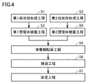
図4は、本発明の実施形態1に係るキャパシタの製造方法を示すフローチャートである。図4に示すように、本発明の実施形態1に係るキャパシタの100製造方法は、第1柱状部形成工程S1と、第1誘電体被覆工程S2と、第2柱状部形成工程S3と、第2誘電体被覆工程S4と、接着剤配置工程S5と、接近工程S6と、固定工程S7とを備えている。
FIG. 4 is a flow chart showing a method of manufacturing a capacitor according to Embodiment 1 of the present invention. As shown in FIG. 4, the method of manufacturing the
図5は、本発明の実施形態1に係るキャパシタの製造方法において、第1支持部に、複数の第1導電柱状部と、第1誘電体層とが設けられた状態を示す図である。図5に示すように、第1柱状部形成工程S1においては、第1導電柱状部112を第1支持部110から成長させる。本実施形態においては、第1支持部110上に配置した触媒粒子から、第1導電柱状部112であるカーボンナノチューブを成長させる。
FIG. 5 is a diagram showing a state in which a plurality of first conductive columnar portions and a first dielectric layer are provided on the first supporting portion in the capacitor manufacturing method according to the first embodiment of the present invention. As shown in FIG. 5, in the first columnar portion forming step S1, the first conductive
触媒粒子は、第1導電柱状部112がカーボンナノチューブである場合はたとえばFe、NiまたはCo、もしくはこれらを含む合金などからなり、第1導電柱状部112がZnOを含む場合はたとえばPtまたはAuもしくはこれらを含む合金などからなる。触媒粒子を配置する方法としては、CVD法、スパッタリングまたはPVD(Physical Vapor Deposition)と、リソグラフィまたはエッチングなどとを組み合わせることが挙げられる。なお、後述する接近工程S6において、第1支持部110から第2支持部120に向かう一方向から見て、当該一方向に垂直な面方向において第1導電柱状部112および第2導電柱状部122が互いに離れて位置するように、触媒粒子の位置はパターニングにより適宜選択される。
The catalyst particles are made of, for example, Fe, Ni, Co, or an alloy containing these when first conductive
複数の第1導電柱状部112の成長方法は特に限定されない。本実施形態において、複数の第1導電柱状部112は、CVDまたはプラズマ強化CVD法などを用いて成長させることができる。CVDまたはプラズマ強化CVD法において使用するガスとしては、一酸化炭素、メタン、エチレン、アセチレン、または、これらと水素あるいはアンモニアの混合物などが挙げられる。
A method for growing the plurality of first conductive
複数の第1導電柱状部112の各々は、触媒粒子の表面から成長する。複数の第1導電柱状部112の各々は、先端113が、第1支持部110から離れていくように、成長する。本実施形態においては、上記1組の複数の触媒粒子に対して、1つの第1導電柱状部112が成長する。
Each of the plurality of first
複数の第1導電柱状部112の各々を、上記CVDまたはプラズマ強化CVD法などを用いて成長させる場合、温度条件およびガス条件などを適宜選択することで、複数の第1導電柱状部112の各々が、所望の範囲内の長さおよび外径を有するように複数の第1導電柱状部112の各々を成長させることができる。ただし、複数の第1導電柱状部112の各々の具体的な長さは、第1支持部110の表面上におけるガスの濃度、ガスの流量、温度のばらつきによって、互いに異なっている。
When each of the plurality of first conductive
なお、複数の第1導電柱状部112の各々は、第1支持部110とは異なる別の基板上に成長させた後、これらの第1導電柱状部112を第1支持部110に化学的または機械的に差し込むようにして移し替えてもよい。この場合、基板と第1導電柱状部112との接合部が、本実施形態に係るキャパシタ100における先端113となる。これにより、先端113を、上記一方向に略垂直な面方向において容易に整列させることができる。
It should be noted that each of the plurality of first
上記基板上において複数の第1導電柱状部112を成長させる方法は、上述した第1支持部110上において複数の第1導電柱状部112を成長させる方法と同様である。また、上記基板を構成する材料としては、たとえば、酸化シリコン、シリコン、ガリウム砒素、アルミニウム、または、SUSなどが挙げられる。
The method for growing the plurality of first conductive
なお、複数の第1導電柱状部112の各々を、カーボンナノチューブを成長させて形成する代わりに、柱状物を金属で薄くコーティングすることで形成してもよい。当該コーティングの具体的な方法としては、ALD(Atomic Layer Deposition)法、CVD(Chemical Vapor Deposition)法、MOCVD(Metalorganic Chemical Vapor Deposition)法、超臨界流体成膜法、めっき法、または導電性ペーストを塗布した後にこれを乾燥させる方法などが挙げられる。
Note that each of the plurality of first conductive
図5に示すように、第1誘電体被覆工程S2においては、第1誘電体層114を、複数の第1導電柱状部112と、第1支持部110において第1導電柱状部112が突出している側の面上とに被覆する。第1誘電体層114の被覆方法は特に限定されず、めっき法、ALD法、CVD法、MOCVD法、超臨界流体成膜法、またはスパッタリングなどが挙げられる。なお、図4に示すように、本実施形態に係るキャパシタ100の製造方法は、第1誘電体被覆工程S2を、後述する接着剤配置工程S5および接近工程S6の前に備えているが、接近工程S6の後に備えていてもよい。
As shown in FIG. 5, in the first dielectric coating step S2, the
図1および図4に示すように、第2柱状部形成工程S3においては、第1柱状部形成工程S1において第1支持部110に第1導電柱状部112を配置することができる方法と同様の方法で、第2支持部120に複数の第2導電柱状部122を配置することができる。第2誘電体被覆工程S4においては、第1誘電体被覆工程S2において第1支持部110および第1導電柱状部112に第1誘電体層114を配置することができる方法と同様の方法で、第2支持部120および第2導電柱状部122に第2誘電体層124を配置することができる。また、図4に示すように、本実施形態に係るキャパシタ100の製造方法は、第2誘電体被覆工程S4を、後述する接着剤配置工程S5および接近工程S6の前に備えているが、接近工程S6の後に備えていてもよい。
As shown in FIGS. 1 and 4, in the second columnar portion forming step S3, the same method as that for disposing the first conductive
図6は、本発明の実施形態1に係るキャパシタの製造方法において、第1支持部と第2支持部との間に、シート状の接着剤を配置した状態を示す図である。図4および図6に示すように、本実施形態の接着剤配置工程S5においては、第2支持部120を第1支持部110に近づける前に、複数の第1導電柱状部112と複数の第2導電柱状部122との間に、接着剤としてシート状接着剤10を配置する。本実施形態においては、複数の第1導電柱状部112の各々の先端113上に設けられた第1誘電体層114上にシート状接着剤10を配置する。
FIG. 6 is a diagram showing a state in which a sheet-like adhesive is arranged between the first support portion and the second support portion in the capacitor manufacturing method according to the first embodiment of the present invention. As shown in FIGS. 4 and 6, in the adhesive disposing step S5 of the present embodiment, before the second supporting
図6に示すように、接近工程S6においては、第2支持部120を第1支持部110に近づける。具体的には、複数の第1導電柱状部112および複数の第2導電柱状部122を、それぞれ第1誘電体層114および第2誘電体層124を介して、シート状接着剤10に押し当てつつ、第2支持部120を第1支持部110に近づける。本実施形態においては、第1誘電体層114が被覆された複数の第1導電柱状部112と、第2誘電体層124が被覆された複数の第2導電柱状部122とが、シート状接着剤10を貫通する。複数の第1導電柱状部112と、複数の第2導電柱状部122とが、シート状接着剤10を貫通した後、さらに、第2支持部120を第1支持部110に近づけることにより、複数の第2導電柱状部122の各々の先端123を、複数の第1導電柱状部112の各々の先端113より、第1支持部110側に配置する。
As shown in FIG. 6, in the approaching step S6, the
本実施形態の接近工程S6においては、シート状接着剤10を加熱して粘度を低下させながら、複数の第1導電柱状部112および複数の第2導電柱状部122を、シート状接着剤10に押し当ててもよい。
In the approaching step S6 of the present embodiment, while the
固定工程S7においては、複数の第1導電柱状部112と複数の第2導電柱状部122とを互いに固定させる。本実施形態においては、上記接着剤を硬化させることにより、複数の第1導電柱状部112と複数の第2導電柱状部122とを互いに固定させる。具体的には、複数の第1導電柱状部112と複数の第2導電柱状部122とを、硬化した接着剤および少なくとも第1誘電体層114と第2誘電体層124とを介して互いに固定させる。シート状接着剤10が、加熱により粘度が低くなる材料で構成されている場合、シート状接着剤10を加熱しながら第2支持部120を第1支持部110に近づけた後に、シート状接着剤10を降温させることで、シート状接着剤10を硬化させてもよい。
In the fixing step S7, the plurality of first conductive
そして、本実施形態においては、上記接着剤が導電性を有している。複数の第1導電柱状部112と複数の第2導電柱状部122とを互いに固定させるときに、硬化した接着剤が導電部130となる。このように、本実施形態においては、導電部130に複数の第1導電柱状部112の各々の一部と複数の第2導電柱状部122の各々の一部とが埋め込まれるように配置されるため、アンカー効果によって、接着剤すなわち導電部130と、複数の第1導電柱状部112の各々および複数の第2導電柱状部122の各々とが互いに強固に接着されている。
In this embodiment, the adhesive has conductivity. The hardened adhesive becomes the
このため、本実施形態において、接着剤すなわち導電部130は、導電性高分子またはAgフィラーなどの金属フィラーを含むペースト状の導電性材料の硬化物で構成されている。
For this reason, in the present embodiment, the adhesive, that is, the
上記の工程により、図1に示すような本発明の実施形態1に係るキャパシタ100が製造される。
Through the above steps, the
上記のように、本発明の実施形態1に係るキャパシタ100においては、複数の第1導電柱状部112の各々は、第1支持部110に支持され、第1支持部110から第2支持部120に向かう一方向に沿って延出している。複数の第2導電柱状部122の各々は、第2支持部120に支持され、第2支持部120から第1支持部110に向かう一方向に沿って延出している。導電部130は、第1誘電体層114上に設けられて複数の第1導電柱状部112の各々の少なくとも一部と第1誘電体層114を介して対向している。導電部130は、第2誘電体層124上に設けられて複数の第2導電柱状部122の各々の少なくとも一部と第2誘電体層124を介して対向している。複数の第2導電柱状部122の各々の先端123は、複数の第1導電柱状部112の各々の先端113より、第1支持部110側に位置している。
As described above, in the
これにより、ナノサイズの外径を有する複数の第1導電柱状部112および複数の第2導電柱状部122を備えるキャパシタ100において、体積容量密度の低下を抑制しつつ耐電圧を向上できる。さらには、このような構成のキャパシタ100は、効率的かつ容易に製造可能である。
As a result, in the
本実施形態に係るキャパシタ100においては、複数の第1導電柱状部112および複数の第2導電柱状部122の少なくとも一方は、カーボンナノチューブからなる。カーボンナノチューブからなる導電柱状部は、同等の大きさの金属からなる導電柱状部より、機械的特性に優れるため、キャパシタ100の信頼性を向上できる。
In the
本実施形態に係るキャパシタ100においては、複数の第1導電柱状部112および複数の第2導電柱状部122の両方がカーボンナノチューブからなる。これにより、複数の第1導電柱状部112および複数の第2導電柱状部122の両方の機械的特性を向上できるため、キャパシタ100の信頼性をさらに向上できる。
In the
また、本発明の実施形態1に係るキャパシタ100の製造方法は、第2支持部120を第1支持部110に近づける接近工程S6と、複数の第1導電柱状部112と複数の第2導電柱状部122とを互いに固定させる固定工程S7とを備えている。接近工程S6においては、第2支持部120を第1支持部110に近づけることにより、複数の第2導電柱状部122の各々の先端を、複数の第1導電柱状部112の各々の先端より、第1支持部110側に配置する。固定工程S7においては、複数の第1導電柱状部112と複数の第2導電柱状部122とを、接着剤および少なくとも第1誘電体層114と第2誘電体層124とを介して互いに固定させる。
In addition, the method for manufacturing the
これにより、体積容量密度の低下が抑制されつつ耐電圧が向上された本発明の実施形態1に係るキャパシタ100を、効率的かつ容易に製造することができる。
This makes it possible to efficiently and easily manufacture the
本実施形態に係るキャパシタ100の製造方法においては、接着剤が導電性を有している。複数の第1導電柱状部112と複数の第2導電柱状部122とを互いに固定させるときに、硬化した接着剤が導電部130となる。これにより、第1誘電体層114および第2誘電体層124の各々の表面に、導電部130を別途被覆することなく、複数の第1導電柱状部112および複数の第2導電柱状部122の各々の対向電極を設けることができる。
In the method of manufacturing the
本実施形態に係るキャパシタ100の製造方法は、第2支持部120を第1支持部110に近づける前に、複数の第1導電柱状部112と複数の第2導電柱状部122との間に、接着剤としてシート状接着剤を配置する接着剤配置工程S5をさらに備えている。第2支持部120を第1支持部110に近づけるときには、複数の第1導電柱状部112および複数の第2導電柱状部122をシート状接着剤に押し当てつつ、第2支持部120を第1支持部110に近づける。
In the method of manufacturing the
これにより、接着剤を設けつつ、第1支持部110側に設けられた部材に対して、第2支持部120側に設けられた部材の相対的な位置を決めることができ、効率よくキャパシタ100を製造できる。
As a result, it is possible to determine the relative position of the member provided on the side of the
(実施形態2)
以下、本発明の実施形態2に係るキャパシタについて説明する。本発明の実施形態2に係るキャパシタは、導電柱状部に対する導電部の相対的な位置が、本発明の実施形態1に係るキャパシタ100と異なっている。よって、本発明の実施形態1に係るキャパシタ100と同様である構成については説明を繰り返さない。(Embodiment 2)
A capacitor according to Embodiment 2 of the present invention will be described below. The capacitor according to Embodiment 2 of the present invention differs from the
図7は、本発明の実施形態2に係るキャパシタの構成を示す断面図である。図7に示すように、本発明の実施形態2に係るキャパシタ200において、導電部230は、第1誘電体層114上および第2誘電体層124上において、少なくとも、第1支持部110から第2支持部120に向かう一方向における複数の第1導電柱状部112の各々の先端113から複数の第2導電柱状部122の各々の先端123まで位置している。
FIG. 7 is a cross-sectional view showing the configuration of a capacitor according to Embodiment 2 of the present invention. As shown in FIG. 7, in the
これにより、複数の第1導電柱状部112および複数の第2導電柱状部122の各々において、導電部230を介した対向面積を増やすことができるため、キャパシタ200の静電容量を大きくできる。また、上記一方向に垂直な面方向において、第1導電柱状部112と第2導電柱状部122とが互いに隣り合うことで形成された隙間全体に導電部230が配置されるため、キャパシタ200内の導電経路の断面積が大きくなり、キャパシタ200における寄生抵抗成分を小さくすることができる。
As a result, the facing area of each of the plurality of first conductive
さらに、本発明の実施形態2に係るキャパシタにおいては、導電部230が、複数の第1導電柱状部112の先端113側において、第1誘電体層114を介して第1導電柱状部112と対向している。また、導電部230が、複数の第2導電柱状部122の先端123側において、第2誘電体層124を介して第2導電柱状部122と対向している。これにより、キャパシタ200の静電容量をさらに大きくできる。
Furthermore, in the capacitor according to the second embodiment of the present invention, the
次に、本発明の実施形態2に係るキャパシタ200の製造方法について説明する。本発明の実施形態2に係るキャパシタ200の製造方法は、本発明の実施形態1に係るキャパシタ100の製造方法と、接近工程S6において異なっている。
Next, a method for manufacturing the
本発明の実施形態2に係るキャパシタ200の製造方法の接近工程においては、第2支持部120を第1支持部110に近づける際に、シート状接着剤10に、複数の第1導電柱状部112および複数の第2導電柱状部122を貫通させずに押し当てる。これにより、シート状接着剤10が、複数の第1導電柱状部112および複数の第2導電柱状部122の各々の形状に沿って変形する。このため、硬化した接着剤すなわち導電部230は、複数の第1導電柱状部112および複数の第2導電柱状部122に対して、上述のように配置される。
In the approaching step of the method for manufacturing the
また、本発明の実施形態2に係るキャパシタ200の製造方法においては、シート状接着剤10が、加熱によりゲル状または液状になる材料で構成されていてもよい。これにより、硬化した接着剤すなわち導電部230を、上述のように、容易に配置できる。
Further, in the method of manufacturing the
(実施形態3)
以下、本発明の実施形態3に係るキャパシタについて説明する。本発明の実施形態3に係るキャパシタは、主に、導電柱状部の長さが本発明の実施形態1に係るキャパシタ100と異なっている。よって、本発明の実施形態1に係るキャパシタ100と同様である構成については説明を繰り返さない。(Embodiment 3)
A capacitor according to Embodiment 3 of the present invention will be described below. The capacitor according to Embodiment 3 of the present invention mainly differs from the
図8は、本発明の実施形態3に係るキャパシタの構成を示す断面図である。図8に示すように、本発明の実施形態3に係るキャパシタ300においては、導電部330が、複数の第1導電柱状部312の先端113側において、第1誘電体層114を介して第1導電柱状部312と対向している。また、本発明の実施形態3に係るキャパシタ300においては、複数の第1導電柱状部312の各々の長さ寸法は、複数の第1支持部110と第2支持部120との離間距離の0.6倍の寸法より大きい。これにより、キャパシタ300の体積容量密度の低下を抑制できる。
FIG. 8 is a cross-sectional view showing the configuration of a capacitor according to Embodiment 3 of the present invention. As shown in FIG. 8, in a
なお、本実施形態においても、複数の第2導電柱状部122の各々の先端123は、複数の第1導電柱状部312の各々の先端113より、第1支持部110側に位置している。これにより、本発明の実施形態1に係るキャパシタ100と同様に、キャパシタ300においても、体積容量密度の低下を抑制しつつ耐電圧を向上できる。さらには、このような構成のキャパシタ300は、効率的かつ容易に製造可能である。
Also in this embodiment, the
(実施形態4)
以下、本発明の実施形態4に係るキャパシタについて説明する。本発明の実施形態4に係るキャパシタは、主に、導電柱状部の長さが本発明の実施形態1に係るキャパシタ100と異なっている。よって、本発明の実施形態1に係るキャパシタ100と同様である構成については説明を繰り返さない。(Embodiment 4)
A capacitor according to Embodiment 4 of the present invention will be described below. The capacitor according to Embodiment 4 of the present invention is mainly different from the
図9は、本発明の実施形態4に係るキャパシタの構成を示す断面図である。図9に示すように、本発明の実施形態4に係るキャパシタ400においては、複数の第1導電柱状部412および複数の第2導電柱状部422の各々の長さ寸法は、複数の第1支持部110と第2支持部120との離間距離の0.9倍の寸法より大きい。これにより、キャパシタ400の体積容量密度の低下を抑制できる。
FIG. 9 is a cross-sectional view showing the configuration of a capacitor according to Embodiment 4 of the present invention. As shown in FIG. 9, in the
なお、本実施形態においても、複数の第2導電柱状部122の各々の先端123は、複数の第1導電柱状部412の各々の先端113より、第1支持部110側に位置している。これにより、本発明の実施形態1に係るキャパシタ100と同様に、キャパシタ400においても、体積容量密度の低下を抑制しつつ耐電圧を向上できる。さらには、このような構成のキャパシタ400は、効率的かつ容易に製造可能である。
Also in this embodiment, the
(実施形態5)
以下、本発明の実施形態5に係るキャパシタについて説明する。本発明の実施形態5に係るキャパシタは、主に、導電部の位置が、本発明の実施形態2に係るキャパシタ200と異なっている。よって、本発明の実施形態2に係るキャパシタ200と同様である構成については説明を繰り返さない。(Embodiment 5)
A capacitor according to Embodiment 5 of the present invention will be described below. The capacitor according to Embodiment 5 of the present invention differs from the
図10は、本発明の実施形態5に係るキャパシタの構成を示す断面図である。図10に示すように、本発明の実施形態5に係るキャパシタ500において、導電部530は、複数の第1導電柱状部112の各々の全体と第1誘電体層114を介して対向し、かつ、第2導電柱状部122の各々の全体と第2誘電体層124を介して対向している。これにより、複数の第1導電柱状部112および複数の第2導電柱状部122の各々において、導電部530との対向面積をさらに増やすことができるため、キャパシタ500の静電容量をより一層大きくできる。
FIG. 10 is a cross-sectional view showing the configuration of a capacitor according to Embodiment 5 of the present invention. As shown in FIG. 10, in the
次に、本発明の実施形態5に係るキャパシタ500の製造方法について説明する。本発明の実施形態5に係るキャパシタ500の製造方法は、本発明の実施形態2に係るキャパシタ200の製造方法と同じ方法を採用できるが、接着剤配置工程S5、接近工程S6および固定工程S7においては、これと異なる方法を採用することができる。
Next, a method for manufacturing the
本発明の実施形態5に係るキャパシタ500の製造方法の変形例においては、接着剤配置工程S5を備えていない。この接着剤配置工程S5に代えて、本発明の実施形態5に係るキャパシタ500の製造方法の変形例は、複数の第2導電柱状部122の各々の先端123を、複数の第1導電柱状部112の各々の先端113より、第1支持部110側に位置させた後、接着剤として液状またはゲル状の接着剤を、第1支持部110と第2支持部120との間に流し込む工程をさらに備える。
The modification of the method for manufacturing the
これにより、第1支持部110から第2支持部120に向かう一方向において、第1導電柱状部112の先端113と第2支持部120との間、または、第2導電柱状部122の先端113と第1支持部110との間など、第1誘電体層114と第2誘電体層124との間の隙間全体に、接着剤を設けることができる。この接着剤が硬化して導電部530となる場合には、複数の第1導電柱状部112および複数の第2導電柱状部122の、導電部530を介した対向面積を向上できる。
As a result, in one direction from the
本実施形態に係るキャパシタ500の製造方法の変形例で用いる接着剤が、加熱により液状またはゲル状となる場合においては、上述の流込工程において、予め加熱された接着剤を流し込んでもよいし、接着剤を加熱しながら流し込んでもよい。
In the case where the adhesive used in the modified example of the method for manufacturing the
なお、本発明の実施形態5に係るキャパシタ500の製造方法の変形例においては、上記の流込工程により接着剤を配置するため、第2支持部120を第1支持部110に近づける工程において、複数の第1導電柱状部112および複数の第2導電柱状部122をシート状接着剤10に押し当てることを要しない。
In addition, in the modification of the method for manufacturing the
(実施形態6)
以下、本発明の実施形態6に係るキャパシタについて説明する。本発明の実施形態6に係るキャパシタは、一部の柱状部を構成する材料が、本発明の実施形態5に係るキャパシタ500と異なっている。よって、本発明の実施形態5に係るキャパシタ500と同様である構成については説明を繰り返さない。(Embodiment 6)
A capacitor according to Embodiment 6 of the present invention will be described below. The capacitor according to the sixth embodiment of the present invention differs from the
図11は、本発明の実施形態6に係るキャパシタの構成を示す断面図である。図11に示すように、本発明の実施形態6に係るキャパシタ600においては、複数の第1導電柱状部612および複数の第2導電柱状部622のいずれか一方が、金属からなる。これにより、第1導電柱状部612または第2導電柱状部622のいずれかがカーボンナノチューブとは異なる導電柱状部であっても、体積容量密度の低下を抑制しつつ耐電圧を向上できる。なお、本実施形態においては、具体的には、複数の第2導電柱状部622の各々が金属で構成されている。
FIG. 11 is a cross-sectional view showing the configuration of a capacitor according to Embodiment 6 of the present invention. As shown in FIG. 11, in a
本実施形態において、金属で構成される複数の第2導電柱状部622は、以下のように設けられる。すなわち、本発明の実施形態1に係るキャパシタ100の製造方法と同様にして、第1柱状部形成工程S1および第1誘電体被覆工程S2により設けられた第1誘電体層114上に、ALD法、MOCVD法、または、超臨界流体成膜法などにより、導電部630を積層する。そして、積層された導電部630に対して、化学的なエッチングにより、凹部を形成する。凹部が形成された導電部630上において、さらに、凹部の形状に沿って第2誘電体層124が被覆される。そして、凹部上に形成された第2誘電体層124上に、さらに、第2導電柱状部622を設ける。そして最後に、第2誘電体層124および第2導電柱状部622上に、第2支持部120を設ければよい。
In this embodiment, the plurality of second conductive
(実施形態7)
以下、本発明の実施形態7に係るキャパシタについて説明する。本発明の実施形態7に係るキャパシタは、導電部が2つに分かれている点が、主に、本発明の実施形態1に係るキャパシタ100と異なる。よって、本発明の実施形態1に係るキャパシタ100と同様である構成については説明を繰り返さない。(Embodiment 7)
A capacitor according to Embodiment 7 of the present invention will be described below. The capacitor according to Embodiment 7 of the present invention mainly differs from the
図12は、本発明の実施形態7に係るキャパシタの構成を示す断面図である。図12に示すように、本発明の実施形態7に係るキャパシタ700は、導電部の一部分として第1導電体層731を備え、導電部の他の部分として第2導電体層732を備えている。第1導電体層731は、第1誘電体層114上の全体にわたって形成されている。第2導電体層732は、第2誘電体層124上の全体にわたって形成されている。
FIG. 12 is a cross-sectional view showing the configuration of a capacitor according to Embodiment 7 of the present invention. As shown in FIG. 12, a
第1導電体層731および第2導電体層732の各々を構成する材料は特に限定されない。第1導電体層731および第2導電体層732の各々を構成する材料としては、銀、金、銅、白金、アルミニウム、または、これらを含む合金などが挙げられる。
Materials forming each of the
本発明の実施形態7に係るキャパシタ700は、さらに、中間固定部740を備えている。中間固定部740は、導電材料で構成されていてもよいし、絶縁材料で構成されていてもよい。中間固定部740が導電材料で構成されている場合は、第1導電体層731と第2導電体層732とが互いに電気的に接続されるため、キャパシタ700は、2つのキャパシタが接続された構成を有することができる。
The
中間固定部740の具体的な位置は、複数の第1導電柱状部112および複数の第2導電柱状部122の各々を間接的に互いに固定していれば特に限定されない。上記の一方向において、複数の第1導電柱状部112の先端113と複数の第2導電柱状部122の先端123との間にのみ位置していもよいし、上記の一方向において、第1支持部110と第2支持部120との間において第1導電体層731と第2導電体層732との間を埋めるように位置していもよい。
A specific position of the
中間固定部740の形成方法は特に限定されないが、本発明の実施形態1に係るキャパシタ100の導電部130または本発明の実施形態5に係るキャパシタ500の導電部530を形成する方法と同様の方法を採用することができる。
The method of forming the
また、本発明の実施形態7に係るキャパシタ700においても、本発明の実施形態1に係るキャパシタ100と同様に、第1導電柱状部112の各々の先端113の位置が、第2支持部120に近いほど好ましく、第2導電柱状部122の各々の先端123の位置が、第1支持部110に近いほど好ましいが、少なくとも、複数の第2導電柱状部122の各々の先端123は、複数の第1導電柱状部112の各々の先端113より、第1支持部110側に位置していればよい。
Also, in the
図13は、本発明の実施形態7の第1変形例に係るキャパシタの構成を示す断面図である。図13に示すように、本発明の実施形態7の変形例に係るキャパシタ700aにおいては、第1支持部110から第2支持部120に向かう一方向において、複数の第1導電柱状部112の各々の先端113の位置と、複数の第2導電柱状部122の各々の先端123との離間距離の位置との差の寸法は、第1支持部110と第2支持部120との離間距離の0.6倍以下である。しかしながら、複数の第2導電柱状部122の各々の先端123は、複数の第1導電柱状部112の各々の先端113より、第1支持部110側に位置しているため、本実施形態においても、体積容量密度の低下を抑制しつつ耐電圧を向上できる。
FIG. 13 is a cross-sectional view showing the configuration of a capacitor according to a first modification of Embodiment 7 of the present invention. As shown in FIG. 13, in a
本発明の実施形態7に係るキャパシタ700の製造方法は、第2支持部120を第1支持部110に近づける前に、第1誘電体層114上に第1導電体層731を積層する工程と、第2誘電体層124上に第2導電体層732を積層する工程とをさらに備えている。これらの積層工程で積層された第1導電体層731および第2導電体層732は、それぞれ、第1誘電体層114および第2誘電体層124との界面での密着性が高い。当該密着性の高さにより、これらの界面においては気泡の発生が抑制されている。一方で、本発明の実施形態1に係るキャパシタ100においては、接着剤からなる導電部130を第1誘電体層114および第2誘電体層124に接着させたときに、接着界面で気泡が発生する。このように、本発明の実施形態7に係るキャパシタ700の上記界面においては、第1導電体層731または第2導電体層732からなる対向電極の有効面積に影響を与える気泡が生じていないため、体積容量密度の低下をより抑制することができる。また、本発明の実施形態7においては、本発明の実施形態1に係るキャパシタ100とは異なる製造方法によって、体積容量密度の低下を抑制しつつ耐電圧を向上させたキャパシタ700を、効率的かつ容易に製造できる。
A method for manufacturing a
すなわち、本実施形態において、第1導電体層731および第2導電体層732の各々は、それぞれ、第1誘電体被覆工程S2および第2誘電体被覆工程S4の直後に形成すればよい。なお、第1導電体層731および第2導電体層732の積層方法は特に限定されない。第1導電体層731および第2導電体層732の各々は、たとえばALD法、CVD法、MOCVD法、超臨界流体成膜法、またはスパッタリング法などにより形成される。
That is, in this embodiment, the
(実施形態8)
以下、本発明の実施形態8に係るキャパシタについて説明する。本発明の実施形態8に係るキャパシタは、固定層をさらに備えている点が、本発明の実施形態7に係るキャパシタ700と異なる。よって、本発明の実施形態7に係るキャパシタ700と同様である構成については説明を繰り返さない。(Embodiment 8)
A capacitor according to Embodiment 8 of the present invention will be described below. The capacitor according to Embodiment 8 of the present invention differs from the
図14は、本発明の実施形態8に係るキャパシタの構成を示す断面図である。図14に示すように、本発明の実施形態8に係るキャパシタ800は、さらに固定層850を備えている。本実施形態において、固定層850は、第1導電体層731と中間固定部740との間に位置している。固定層850は、第2導電体層732と中間固定部740との間にも位置している。固定層850を設けることにより、複数の第1導電柱状部112の各々と複数の第2導電柱状部122の各々が自重または外部からの機械的な外力により変形することを抑制することができる。
FIG. 14 is a cross-sectional view showing the configuration of a capacitor according to Embodiment 8 of the present invention. As shown in FIG. 14, the
本実施形態において、固定層850は絶縁材料で構成されている。これにより、中間固定部740が絶縁材料で構成されている場合には、キャパシタ800は、体積あたりの容量密度を増加させつつ、互いに独立した2つのキャパシタを備えることができる。また、固定層850は導電材料で構成されていてもよい。さらに中間固定部740が導電材料で構成されている場合には、キャパシタ700の機械的強度を向上させるとともに、2つのキャパシタを直列接続することができる。
In this embodiment, the fixed
(実施形態9)
以下、本発明の実施形態9に係るキャパシタについて説明する。本発明の実施形態9に係るキャパシタは、主に、各柱状部の構成が、本発明の実施形態1に係るキャパシタ100と異なる。よって、本発明の実施形態1に係るキャパシタ100と同様である構成については説明を繰り返さない。(Embodiment 9)
A capacitor according to Embodiment 9 of the present invention will be described below. A capacitor according to Embodiment 9 of the present invention differs from
図15は、本発明の実施形態9に係るキャパシタの構成を示す断面図である。図15に示すように、本発明の実施形態9に係るキャパシタ900においては、複数の第2導電柱状部122の各々の長さが互いに異なっている。本発明の実施形態9に係るキャパシタ900においても、複数の第2導電柱状部122の各々の先端123は、複数の第1導電柱状部112の各々の先端113より、第1支持部110側に位置している。よって、本実施形態に係るキャパシタ900においても、体積容量密度の低下を抑制しつつ耐電圧を向上できる。さらには、このような構成のキャパシタ900は、効率的かつ容易に製造可能である。
FIG. 15 is a cross-sectional view showing the configuration of a capacitor according to Embodiment 9 of the present invention. As shown in FIG. 15, in a
(実施形態10)
以下、本発明の実施形態10に係るキャパシタについて説明する。本発明の実施形態10に係るキャパシタは、主に、各柱状部の構成が、本発明の実施形態9に係るキャパシタ900と異なる。よって、本発明の実施形態9に係るキャパシタ900と同様である構成については説明を繰り返さない。(Embodiment 10)
A capacitor according to
図16は、本発明の実施形態10に係るキャパシタの構成を示す断面図である。図16に示すように、本発明の実施形態10に係るキャパシタ1000においては、複数の第2導電柱状部122の少なくとも1つが、先端123において、第2誘電体層124を介して、第1誘電体層114と接触している。これにより、キャパシタ1000の機械強度が向上する。なお、複数の第1導電柱状部112の少なくとも1つが、先端113において、第1誘電体層114を介して、第2誘電体層124と接触していてもよい。
FIG. 16 is a cross-sectional view showing the configuration of a capacitor according to
(実施形態11)
以下、本発明の実施形態11に係るキャパシタについて説明する。本発明の実施形態11に係るキャパシタは、主に、各柱状部の構成が、本発明の実施形態10に係るキャパシタ1000と異なる。よって、本発明の実施形態10に係るキャパシタ1000と同様である構成については説明を繰り返さない。(Embodiment 11)
A capacitor according to Embodiment 11 of the present invention will be described below. The capacitor according to the eleventh embodiment of the present invention mainly differs from the
図17は、本発明の実施形態11に係るキャパシタの構成を示す断面図である。図17に示すように、本発明の実施形態11に係るキャパシタ1100においては、複数の第2導電柱状部122の少なくとも1つが、先端123側において、第2誘電体層124を介して、第1誘電体層114と接触しつつ湾曲している。これにより、キャパシタ1100の機械強度が向上するとともに、第1支持部110から第2支持部120に向かう一方向における、第1導電柱状部112と第2導電柱状部122との接着強度が向上する。なお、複数の第1導電柱状部112の少なくとも1つが、先端113側において、第1誘電体層114を介して、第2誘電体層124と接触しつつ湾曲してもよい。
FIG. 17 is a cross-sectional view showing the configuration of a capacitor according to Embodiment 11 of the present invention. As shown in FIG. 17, in the
上述した実施形態の説明において、組み合わせ可能な構成を相互に組み合わせてもよい。 In the description of the above embodiments, combinable configurations may be combined with each other.
今回開示された実施形態はすべての点で例示であって制限的なものではないと考えられるべきである。本発明の範囲は上記した説明ではなくて請求の範囲によって示され、請求の範囲と均等の意味および範囲内でのすべての変更が含まれることが意図される。 It should be considered that the embodiments disclosed this time are illustrative in all respects and not restrictive. The scope of the present invention is indicated by the scope of the claims rather than the above description, and is intended to include all changes within the scope and meaning equivalent to the scope of the claims.
10 シート状接着剤、100,100a,200,300,400,500,600,700,700a,800,900,1000,1100 キャパシタ、110 第1支持部、112,312,412,612 第1導電柱状部、113,123 先端、114 第1誘電体層、120 第2支持部、122,422,622 第2導電柱状部、124 第2誘電体層、130,230,330,530,630 導電部、731 第1導電体層、732 第2導電体層、740 中間固定部、850 固定層。
10
Claims (11)
前記第1支持部に間隔をあけて位置する第2支持部と、
前記第1支持部に支持され、前記第1支持部から前記第2支持部に向かう一方向に沿って延出し、かつ、ナノサイズの外径を有する、複数の第1導電柱状部と、
前記複数の第1導電柱状部の各々を被覆する第1誘電体層と、
前記第2支持部に支持され、前記第2支持部から前記第1支持部に向かう前記一方向に沿って延出し、かつ、ナノサイズの外径を有する、複数の第2導電柱状部と、
前記複数の第2導電柱状部の各々を被覆する第2誘電体層と、
前記第1誘電体層上に設けられて前記複数の第1導電柱状部の各々の少なくとも一部と前記第1誘電体層を介して対向し、かつ、前記第2誘電体層上に設けられて前記複数の第2導電柱状部の各々の少なくとも一部と前記第2誘電体層を介して対向する、導電部とを備え、
前記複数の第2導電柱状部の各々の先端は、前記複数の第1導電柱状部の各々の先端より、第1支持部側に位置している、キャパシタ。a first support;
a second support spaced apart from the first support;
a plurality of first conductive columnar portions supported by the first support portion, extending along one direction from the first support portion toward the second support portion, and having nano-sized outer diameters;
a first dielectric layer covering each of the plurality of first conductive columns;
a plurality of second conductive columnar portions supported by the second support portion, extending along the one direction from the second support portion toward the first support portion, and having nano-sized outer diameters;
a second dielectric layer covering each of the plurality of second conductive pillars;
provided on the first dielectric layer to face at least a portion of each of the plurality of first conductive columnar portions through the first dielectric layer, and provided on the second dielectric layer; a conductive portion facing at least a portion of each of the plurality of second conductive columnar portions with the second dielectric layer interposed therebetween;
The capacitor, wherein the tip of each of the plurality of second conductive columnar portions is located closer to the first support portion than the tip of each of the plurality of first conductive columnar portions.
前記第2誘電体層は、前記第2支持部上において前記複数の第1導電柱状部の各々の全体を被覆しており、
前記導電部は、前記複数の第1導電柱状部の各々の全体と前記第1誘電体層を介して対向し、かつ、前記第2導電柱状部の各々の全体と前記第2誘電体層を介して対向する、請求項1から請求項5のいずれか1項に記載のキャパシタ。the first dielectric layer covering the entirety of each of the plurality of first conductive columnar portions on the first supporting portion;
the second dielectric layer covering the entirety of each of the plurality of first conductive columnar portions on the second supporting portion;
The conductive portion faces the entirety of each of the plurality of first conductive columnar portions through the first dielectric layer, and the entirety of each of the second conductive columnar portions and the second dielectric layer. 6. The capacitor according to any one of claims 1 to 5, facing through.
前記第1支持部に支持され、前記第1支持部から離れる一方向に沿って延出し、かつ、ナノサイズの外径を有する、複数の第1導電柱状部と、
前記複数の第1導電柱状部の各々を被覆する第1誘電体層と、
第2支持部と、
前記第2支持部に支持され、前記第2支持部から離れる一方向に沿って延出し、かつ、ナノサイズの外径を有する、複数の第2導電柱状部と、
前記複数の第2導電柱状部の各々を被覆する第2誘電体層と、
前記第1誘電体層上に設けられて前記複数の第1導電柱状部の各々の少なくとも一部と前記第1誘電体層を介して対向し、かつ、前記第2誘電体層上に設けられて前記複数の第2導電柱状部の各々の少なくとも一部と前記第2誘電体層を介して対向する導電部とを備える、キャパシタの製造方法であって、
前記第2支持部を前記第1支持部に近づけることにより、前記複数の第2導電柱状部の各々の先端を、前記複数の第1導電柱状部の各々の先端より、第1支持部側に配置する工程と、
前記複数の第1導電柱状部と前記複数の第2導電柱状部とを、接着剤および少なくとも前記第1誘電体層と前記第2誘電体層とを介して互いに固定させる工程とを備える、キャパシタの製造方法。a first support;
a plurality of first conductive pillars supported by the first support, extending along one direction away from the first support, and having nano-sized outer diameters;
a first dielectric layer covering each of the plurality of first conductive columns;
a second support;
a plurality of second conductive pillars supported by the second support, extending along one direction away from the second support, and having nano-sized outer diameters;
a second dielectric layer covering each of the plurality of second conductive pillars;
provided on the first dielectric layer to face at least a portion of each of the plurality of first conductive columnar portions through the first dielectric layer, and provided on the second dielectric layer; a conductive portion facing at least a portion of each of the plurality of second conductive columnar portions via the second dielectric layer, the method comprising:
By bringing the second support portion close to the first support portion, the tip of each of the plurality of second conductive columnar portions is moved closer to the first support portion than the tip of each of the plurality of first conductive columnar portions. arranging;
fixing the plurality of first conductive pillars and the plurality of second conductive pillars to each other via an adhesive and at least the first dielectric layer and the second dielectric layer. manufacturing method.
前記複数の第1導電柱状部と前記複数の第2導電柱状部とを互いに固定させるときに、硬化した前記接着剤が前記導電部となる、請求項7に記載のキャパシタの製造方法。The adhesive has conductivity,
8. The method of manufacturing a capacitor according to claim 7, wherein the hardened adhesive becomes the conductive portion when the plurality of first conductive columnar portions and the plurality of second conductive columnar portions are fixed to each other.
前記第2支持部を前記第1支持部に近づける前に、前記導電部の他の部分として、前記第2誘電体層上に第2導電体層を積層する工程とをさらに備える、請求項7に記載のキャパシタの製造方法。Laminating a first conductive layer on the first dielectric layer as part of the conductive portion before bringing the second support portion closer to the first support portion;
8. The step of stacking a second conductive layer on the second dielectric layer as another portion of the conductive portion before bringing the second support portion close to the first support portion. A method for manufacturing the capacitor according to 1.
前記第2支持部を前記第1支持部に近づけるときに、前記複数の第1導電柱状部および前記複数の第2導電柱状部を前記シート状接着剤に押し当てつつ、前記第2支持部を前記第1支持部に近づける、請求項7から請求項9のいずれか1項に記載のキャパシタの製造方法。disposing a sheet adhesive as the adhesive between the plurality of first conductive columnar portions and the plurality of second conductive columnar portions before bringing the second support portion close to the first support portion; further comprising
When the second support portion is brought closer to the first support portion, the second support portion is pushed while pressing the plurality of first conductive columnar portions and the plurality of second conductive columnar portions against the sheet adhesive. 10. The method of manufacturing a capacitor according to any one of claims 7 to 9, wherein the first support portion is brought closer.
Applications Claiming Priority (3)
| Application Number | Priority Date | Filing Date | Title |
|---|---|---|---|
| JP2019174347 | 2019-09-25 | ||
| JP2019174347 | 2019-09-25 | ||
| PCT/JP2020/016272 WO2021059569A1 (en) | 2019-09-25 | 2020-04-13 | Capacitor and method for manufacturing same |
Publications (2)
| Publication Number | Publication Date |
|---|---|
| JPWO2021059569A1 JPWO2021059569A1 (en) | 2021-04-01 |
| JP7151907B2 true JP7151907B2 (en) | 2022-10-12 |
Family
ID=75166937
Family Applications (1)
| Application Number | Title | Priority Date | Filing Date |
|---|---|---|---|
| JP2021548315A Active JP7151907B2 (en) | 2019-09-25 | 2020-04-13 | Capacitor and manufacturing method thereof |
Country Status (3)
| Country | Link |
|---|---|
| US (1) | US11749463B2 (en) |
| JP (1) | JP7151907B2 (en) |
| WO (1) | WO2021059569A1 (en) |
Families Citing this family (1)
| Publication number | Priority date | Publication date | Assignee | Title |
|---|---|---|---|---|
| WO2021059569A1 (en) * | 2019-09-25 | 2021-04-01 | 株式会社村田製作所 | Capacitor and method for manufacturing same |
Citations (5)
| Publication number | Priority date | Publication date | Assignee | Title |
|---|---|---|---|---|
| JP2003234254A (en) | 2002-02-07 | 2003-08-22 | Hitachi Zosen Corp | Electrical double layer capacitor using carbon nano-tube |
| JP2005129566A (en) | 2003-10-21 | 2005-05-19 | Toyota Motor Corp | Capacitor |
| JP2008193096A (en) | 2007-02-06 | 2008-08-21 | Young Joo Oh | Metal capacitor and manufacturing method therefor |
| JP2015514315A (en) | 2012-03-22 | 2015-05-18 | カリフォルニア インスティチュート オブ テクノロジー | Micro / nanoscale capacitors comprising an array of conductive elements having elongated bodies |
| JP2015519742A (en) | 2012-05-03 | 2015-07-09 | ダイソン テクノロジー リミテッド | Hybrid capacitor |
Family Cites Families (10)
| Publication number | Priority date | Publication date | Assignee | Title |
|---|---|---|---|---|
| EP1538640B1 (en) * | 2003-12-05 | 2016-11-16 | NGK Spark Plug Co., Ltd. | Capacitor and method for manufacturing the same |
| JP5091242B2 (en) | 2006-10-04 | 2012-12-05 | エヌエックスピー ビー ヴィ | MIM capacitor |
| JP4357577B2 (en) * | 2007-06-14 | 2009-11-04 | 太陽誘電株式会社 | Capacitor and manufacturing method thereof |
| JP5931594B2 (en) * | 2012-06-07 | 2016-06-08 | 太陽誘電株式会社 | Capacitor |
| US9119289B2 (en) * | 2013-02-25 | 2015-08-25 | 3M Innovative Properties Company | Film constructions for interdigitated electrodes with bus bars and methods of making same |
| WO2021059569A1 (en) * | 2019-09-25 | 2021-04-01 | 株式会社村田製作所 | Capacitor and method for manufacturing same |
| WO2021059570A1 (en) * | 2019-09-25 | 2021-04-01 | 株式会社村田製作所 | Nanostructure aggregate and method for manufacturing same |
| WO2021079565A1 (en) * | 2019-10-24 | 2021-04-29 | 株式会社村田製作所 | Composite capacitor |
| WO2021079566A1 (en) * | 2019-10-24 | 2021-04-29 | 株式会社村田製作所 | Composite capacitor |
| US11715594B2 (en) * | 2021-05-27 | 2023-08-01 | International Business Machines Corporation | Vertically-stacked interdigitated metal-insulator-metal capacitor for sub-20 nm pitch |
-
2020
- 2020-04-13 WO PCT/JP2020/016272 patent/WO2021059569A1/en active Application Filing
- 2020-04-13 JP JP2021548315A patent/JP7151907B2/en active Active
-
2022
- 2022-03-03 US US17/653,392 patent/US11749463B2/en active Active
Patent Citations (5)
| Publication number | Priority date | Publication date | Assignee | Title |
|---|---|---|---|---|
| JP2003234254A (en) | 2002-02-07 | 2003-08-22 | Hitachi Zosen Corp | Electrical double layer capacitor using carbon nano-tube |
| JP2005129566A (en) | 2003-10-21 | 2005-05-19 | Toyota Motor Corp | Capacitor |
| JP2008193096A (en) | 2007-02-06 | 2008-08-21 | Young Joo Oh | Metal capacitor and manufacturing method therefor |
| JP2015514315A (en) | 2012-03-22 | 2015-05-18 | カリフォルニア インスティチュート オブ テクノロジー | Micro / nanoscale capacitors comprising an array of conductive elements having elongated bodies |
| JP2015519742A (en) | 2012-05-03 | 2015-07-09 | ダイソン テクノロジー リミテッド | Hybrid capacitor |
Also Published As
| Publication number | Publication date |
|---|---|
| US20220189702A1 (en) | 2022-06-16 |
| US11749463B2 (en) | 2023-09-05 |
| WO2021059569A1 (en) | 2021-04-01 |
| JPWO2021059569A1 (en) | 2021-04-01 |
Similar Documents
| Publication | Publication Date | Title |
|---|---|---|
| JP7248143B2 (en) | Composite capacitor | |
| JP5875244B2 (en) | Electromechanical transducer and method for manufacturing the same | |
| US7999446B1 (en) | Piezoelectronic device and method of fabricating the same | |
| JP5665618B2 (en) | Capacitor configuration unit and capacitor | |
| JP5408881B2 (en) | Piezoelectric multilayer element | |
| JP7151907B2 (en) | Capacitor and manufacturing method thereof | |
| US8106566B2 (en) | Piezoelectric component with outer contacting, having gas-phase deposition, method for manufacturing component and use of component | |
| JP2005168281A5 (en) | ||
| TW201103179A (en) | Stacked-type piezoelectric device and method for manufacturing the same | |
| US20230340647A1 (en) | Bonding structure and method of manufacturing bonding structure | |
| WO2021059570A1 (en) | Nanostructure aggregate and method for manufacturing same | |
| JP5665617B2 (en) | Capacitor configuration unit and capacitor | |
| Chen et al. | Through-silicon-via interposers with Cu-level electrical conductivity and Si-level thermal expansion based on carbon nanotube-Cu composites for microelectronic packaging applications | |
| JP5760668B2 (en) | Sheet-like structure, manufacturing method thereof, electronic device, and manufacturing method thereof | |
| WO2021079566A1 (en) | Composite capacitor | |
| WO2015183762A1 (en) | Chip-scale embedded carbon nanotube electrochemical double layer supercapacitor | |
| JP6156057B2 (en) | Nanostructure sheet, electronic device, method for producing nanostructure sheet, and method for producing electronic device | |
| JP6354235B2 (en) | Electronic device and assembly method thereof, and sheet-like structure and manufacturing method thereof | |
| US11870372B2 (en) | Flexible and hybrid energy harvesting device combining piezoelectric and electrostatic conversions | |
| WO2010090074A1 (en) | Polymer actuator and manufacturing method therefor | |
| CN117650122A (en) | Semiconductor structure and manufacturing method thereof | |
| WO2021229871A1 (en) | Structure | |
| JP3867823B2 (en) | Manufacturing method of laminated piezoelectric element | |
| JP5930533B2 (en) | Polymer actuator and manufacturing method thereof | |
| JP2010278178A (en) | Laminated body of piezoelectric film and method of manufacturing the same |
Legal Events
| Date | Code | Title | Description |
|---|---|---|---|
| A621 | Written request for application examination |
Free format text: JAPANESE INTERMEDIATE CODE: A621 Effective date: 20211109 |
|
| TRDD | Decision of grant or rejection written | ||
| A01 | Written decision to grant a patent or to grant a registration (utility model) |
Free format text: JAPANESE INTERMEDIATE CODE: A01 Effective date: 20220830 |
|
| A61 | First payment of annual fees (during grant procedure) |
Free format text: JAPANESE INTERMEDIATE CODE: A61 Effective date: 20220912 |
|
| R150 | Certificate of patent or registration of utility model |
Ref document number: 7151907 Country of ref document: JP Free format text: JAPANESE INTERMEDIATE CODE: R150 |