JP7151123B2 - Electric storage element inspection method and electric storage element - Google Patents
Electric storage element inspection method and electric storage element Download PDFInfo
- Publication number
- JP7151123B2 JP7151123B2 JP2018060565A JP2018060565A JP7151123B2 JP 7151123 B2 JP7151123 B2 JP 7151123B2 JP 2018060565 A JP2018060565 A JP 2018060565A JP 2018060565 A JP2018060565 A JP 2018060565A JP 7151123 B2 JP7151123 B2 JP 7151123B2
- Authority
- JP
- Japan
- Prior art keywords
- terminal
- storage element
- electrode
- contact
- probe
- Prior art date
- Legal status (The legal status is an assumption and is not a legal conclusion. Google has not performed a legal analysis and makes no representation as to the accuracy of the status listed.)
- Active
Links
Images


Classifications
-
- Y—GENERAL TAGGING OF NEW TECHNOLOGICAL DEVELOPMENTS; GENERAL TAGGING OF CROSS-SECTIONAL TECHNOLOGIES SPANNING OVER SEVERAL SECTIONS OF THE IPC; TECHNICAL SUBJECTS COVERED BY FORMER USPC CROSS-REFERENCE ART COLLECTIONS [XRACs] AND DIGESTS
- Y02—TECHNOLOGIES OR APPLICATIONS FOR MITIGATION OR ADAPTATION AGAINST CLIMATE CHANGE
- Y02E—REDUCTION OF GREENHOUSE GAS [GHG] EMISSIONS, RELATED TO ENERGY GENERATION, TRANSMISSION OR DISTRIBUTION
- Y02E60/00—Enabling technologies; Technologies with a potential or indirect contribution to GHG emissions mitigation
- Y02E60/10—Energy storage using batteries
-
- Y—GENERAL TAGGING OF NEW TECHNOLOGICAL DEVELOPMENTS; GENERAL TAGGING OF CROSS-SECTIONAL TECHNOLOGIES SPANNING OVER SEVERAL SECTIONS OF THE IPC; TECHNICAL SUBJECTS COVERED BY FORMER USPC CROSS-REFERENCE ART COLLECTIONS [XRACs] AND DIGESTS
- Y02—TECHNOLOGIES OR APPLICATIONS FOR MITIGATION OR ADAPTATION AGAINST CLIMATE CHANGE
- Y02P—CLIMATE CHANGE MITIGATION TECHNOLOGIES IN THE PRODUCTION OR PROCESSING OF GOODS
- Y02P70/00—Climate change mitigation technologies in the production process for final industrial or consumer products
- Y02P70/50—Manufacturing or production processes characterised by the final manufactured product
Description
本発明は、蓄電素子の検査方法及び蓄電素子に関する。 TECHNICAL FIELD The present invention relates to an inspection method for an electric storage element and an electric storage element.
従来、蓄電素子の製造工程等において、蓄電素子の電極端子にプローブを接触させて、蓄電素子の電気特性を検査する作業が広く行われている。例えば、特許文献1には、正確な検査を行うために、電圧計測用もしくは通電用の電極(プローブ)の、鉛蓄電池端子(電極端子)との当接面にリブ状突起を形成して、電圧計測や容量検査等を行う検査方法が開示されている。
2. Description of the Related Art Conventionally, in a manufacturing process of an electric storage element, etc., an operation of inspecting electric characteristics of the electric storage element by bringing a probe into contact with an electrode terminal of the electric storage element has been widely performed. For example, in
しかしながら、上記従来の蓄電素子の検査方法では、電気特性の検査精度が低下してしまうおそれがある。例えば、上記特許文献1では、プローブと電極端子との接触不良を抑制するために、プローブの電極端子との当接面にリブ状突起を形成して、検査を行っている。しかし、本願発明者は、この検査を同じプローブを用いて繰り返し行うことで、電極端子の材料がプローブのリブ状突起に付着していき、これにより、プローブと電極端子との接触不良が発生するおそれがあることを見出した。プローブと電極端子との接触不良が発生すれば、蓄電素子の電気特性の検査精度が低下してしまう。
However, in the above-described conventional method for inspecting electric storage elements, there is a risk that the inspection accuracy of electrical characteristics may be degraded. For example, in
本発明は、上記問題に鑑みてなされたものであり、電気特性の検査精度が低下するのを抑制することができる蓄電素子の検査方法及び蓄電素子を提供することを目的とする。 The present invention has been made in view of the above problems, and an object of the present invention is to provide an electric storage element inspection method and an electric storage element capable of suppressing deterioration in inspection accuracy of electrical characteristics.
上記目的を達成するために、本発明の一態様に係る蓄電素子の検査方法は、電極端子を備える蓄電素子の検査方法であって、複数の凸部が面状に形成された前記電極端子の端子表面に、プローブを接触させて、前記蓄電素子の電気特性を検査する検査工程を含む。 To achieve the above object, a method for inspecting a storage element according to one aspect of the present invention is a method for inspecting a storage element having an electrode terminal, the electrode terminal having a plurality of projections formed in a planar shape. It includes an inspection step of inspecting electrical characteristics of the storage element by contacting a probe to the surface of the terminal.
これによれば、蓄電素子の検査方法において、検査工程として、複数の凸部が面状に形成された電極端子の端子表面に、プローブを接触させて、蓄電素子の電気特性を検査する。このように、電極端子の端子表面に複数の凸部が面状に形成された蓄電素子を用いて、当該電極端子の端子表面にプローブを接触させることで、プローブと電極端子との接触不良を抑制することができる。つまり、蓄電素子の電極端子に凸部が設けられているため、同じプローブを用いて繰り返し検査を行った場合でも、プローブと電極端子との接触を確保できる状態を保つことができる。これにより、プローブと電極端子とが接触不良を起こすのを抑制して蓄電素子の電気特性を検査することができるため、電気特性の検査精度が低下するのを抑制することができる。 According to this, in the inspection method of the electric storage element, as the inspection step, the electrical characteristics of the electric storage element are inspected by bringing the probe into contact with the terminal surface of the electrode terminal having the plurality of planar projections. In this way, contact failure between the probe and the electrode terminal can be prevented by bringing the probe into contact with the terminal surface of the electrode terminal using the power storage element in which a plurality of projections are formed in a planar shape on the terminal surface of the electrode terminal. can be suppressed. In other words, since the electrode terminals of the electric storage element are provided with the projections, even when the same probe is used for repeated tests, the contact between the probe and the electrode terminals can be maintained. As a result, it is possible to inspect the electrical characteristics of the electric storage element while suppressing the occurrence of poor contact between the probe and the electrode terminal, so it is possible to suppress deterioration in the inspection accuracy of the electrical characteristics.
また、前記検査工程では、前記端子表面に、前記プローブの平坦面を接触させて、前記蓄電素子の電気特性を検査することにしてもよい。 Further, in the inspection step, the flat surface of the probe may be brought into contact with the surface of the terminal to inspect the electric characteristics of the electric storage element.
これによれば、蓄電素子の検査方法において、検査工程では、複数の凸部が面状に形成された電極端子の端子表面に、プローブの平坦面を接触させて、蓄電素子の電気特性を検査する。このように、プローブの電極端子との当接面が平坦面であるため、同じプローブを用いて繰り返し検査を行った場合でも、電極端子の材料がプローブに付着するのを抑制し、プローブと電極端子との接触を確保できる状態を保つことができる。これにより、プローブと電極端子とが接触不良を起こすのを抑制して蓄電素子の電気特性を検査することができるため、電気特性の検査精度が低下するのを抑制することができる。 According to this, in the inspection method of the storage element, in the inspection step, the flat surface of the probe is brought into contact with the terminal surface of the electrode terminal on which the plurality of convex portions are formed to inspect the electrical characteristics of the storage element. do. As described above, since the contact surface of the probe with the electrode terminal is a flat surface, even when the same probe is used for repeated tests, adhesion of the material of the electrode terminal to the probe is suppressed, and the contact between the probe and the electrode is suppressed. It is possible to maintain a state in which contact with the terminal can be secured. As a result, it is possible to inspect the electrical characteristics of the electric storage element while suppressing the occurrence of poor contact between the probe and the electrode terminal, so it is possible to suppress deterioration in the inspection accuracy of the electrical characteristics.
また、前記検査工程では、前記端子表面に、前記端子表面よりも硬度が高い前記プローブを接触させて、前記蓄電素子の電気特性を検査することにしてもよい。 Further, in the inspection step, the electrical characteristics of the storage element may be inspected by contacting the terminal surface with the probe having a hardness higher than that of the terminal surface.
これによれば、蓄電素子の検査方法において、検査工程では、複数の凸部が面状に形成された電極端子の端子表面に、端子表面よりも硬度が高いプローブを接触させて、蓄電素子の電気特性を検査する。このように、プローブが電極端子の端子表面よりも硬いため、プローブを端子表面に接触させることで、端子表面の複数の凸部がつぶれ、プローブと電極端子との接触を確保することができる。これにより、プローブと電極端子とが接触不良を起こすのを抑制して蓄電素子の電気特性を検査することができるため、電気特性の検査精度が低下するのを抑制することができる。 According to this, in the inspection method of the storage element, in the inspection step, a probe having a higher hardness than the terminal surface is brought into contact with the terminal surface of the electrode terminal on which the plurality of projections are formed in a planar shape, so that the storage element is inspected. Inspect the electrical characteristics. In this way, since the probe is harder than the terminal surface of the electrode terminal, by bringing the probe into contact with the terminal surface, the plurality of protrusions on the terminal surface are crushed, and the contact between the probe and the electrode terminal can be secured. As a result, it is possible to inspect the electrical characteristics of the electric storage element while suppressing the occurrence of poor contact between the probe and the electrode terminal, so it is possible to suppress deterioration in the inspection accuracy of the electrical characteristics.
また、容器と電極端子とを備える蓄電素子であって、前記電極端子は、前記容器とは反対側の面であって他の部材と接合される端子表面を有し、前記端子表面の前記他の部材との接合領域には、複数の凸部が面状に配置されていることにしてもよい。 Further, the electric storage element includes a container and an electrode terminal, wherein the electrode terminal has a terminal surface that is on the opposite side of the container and is joined to another member, and A plurality of projections may be arranged in a plane in the joint area with the member.
これによれば、蓄電素子において、電極端子は、容器とは反対側に端子表面を有しており、端子表面の他の部材との接合領域には、複数の凸部が面状に配置されている。ここで、電極端子の端子表面にプローブを接触させて検査を行う場合には、スペース上の問題から、端子表面における当該接合領域にプローブを接触させることとなる。このため、端子表面の面状に形成された複数の凸部にプローブを接触させることとなり、プローブと電極端子との接触不良を抑制することができる。また、端子表面は、電極端子の容器とは反対側の面であるため、プローブを端子表面に接触させる際に、容器が土台となって、電極端子を安定して支持することができ、端子表面が撓んだり傾いたりするのを抑制することができる。これにより、プローブと電極端子とが接触不良を起こすのを抑制して蓄電素子の電気特性を検査することができるため、電気特性の検査精度が低下するのを抑制することができる。 According to this, in the electric storage element, the electrode terminal has a terminal surface on the side opposite to the container, and a plurality of convex portions are arranged in a planar manner in the joint region of the terminal surface with another member. ing. Here, when the probe is brought into contact with the terminal surface of the electrode terminal for inspection, the probe is brought into contact with the joint region on the terminal surface due to space considerations. For this reason, the probes are brought into contact with the plurality of protrusions formed on the surface of the terminal, and poor contact between the probes and the electrode terminals can be suppressed. In addition, since the surface of the terminal is the surface opposite to the container of the electrode terminal, when the probe is brought into contact with the surface of the terminal, the container serves as a base to stably support the electrode terminal. It is possible to suppress the bending and tilting of the surface. As a result, it is possible to inspect the electrical characteristics of the electric storage element while suppressing the occurrence of poor contact between the probe and the electrode terminal, so it is possible to suppress deterioration in the inspection accuracy of the electrical characteristics.
また、前記複数の凸部のそれぞれは、突出高さが0.1mm以上であることにしてもよい。 Further, each of the plurality of protrusions may have a protrusion height of 0.1 mm or more.
これによれば、蓄電素子において、電極端子の端子表面に配置された複数の凸部のそれぞれは、突出高さが0.1mm以上である。このように、当該凸部の突出高さが0.1mmにも満たない場合には当該凸部はつぶれにくいが、当該凸部が0.1mm以上の高さを有することで、電極端子の端子表面にプローブを接触させて検査を行う際に、当該凸部がつぶれてプローブと電極端子とを接触しやすくすることができる。これにより、プローブと電極端子とが接触不良を起こすのを抑制して蓄電素子の電気特性を検査することができるため、電気特性の検査精度が低下するのを抑制することができる。 According to this, in the electric storage element, each of the plurality of protrusions arranged on the terminal surface of the electrode terminal has a protrusion height of 0.1 mm or more. As described above, when the protrusion height of the protrusion is less than 0.1 mm, the protrusion is difficult to be crushed. When the probe is brought into contact with the surface for inspection, the convex portion is collapsed to facilitate contact between the probe and the electrode terminal. As a result, it is possible to inspect the electrical characteristics of the electric storage element while suppressing the occurrence of poor contact between the probe and the electrode terminal, so it is possible to suppress deterioration in the inspection accuracy of the electrical characteristics.
また、前記複数の凸部のそれぞれは、先端部分が曲面形状を有していることにしてもよい。 Further, each of the plurality of protrusions may have a curved tip portion.
これによれば、蓄電素子において、電極端子の端子表面に配置された複数の凸部のそれぞれは、先端部分が曲面形状を有している。このように、当該凸部の先端部分が曲面形状を有している(尖っていない)ことで、電極端子の端子表面にプローブを接触させて検査を行う際に、電極端子の当該凸部の先端の部材がプローブに付着するのを抑制することができる。これにより、プローブと電極端子とが接触不良を起こすのを抑制して蓄電素子の電気特性を検査することができるため、電気特性の検査精度が低下するのを抑制することができる。 According to this, in the electric storage element, each of the plurality of protrusions arranged on the terminal surface of the electrode terminal has a curved tip portion. In this way, since the tip portion of the projection has a curved surface shape (not sharp), when the terminal surface of the electrode terminal is inspected by bringing the probe into contact with the terminal surface, the projection of the electrode terminal can be It is possible to suppress the tip member from adhering to the probe. As a result, it is possible to inspect the electrical characteristics of the electric storage element while suppressing the occurrence of poor contact between the probe and the electrode terminal, so it is possible to suppress deterioration in the inspection accuracy of the electrical characteristics.
また、前記電極端子は、前記端子表面を有する端子本体と、前記蓄電素子の容器を貫通する軸部とを有し、前記複数の凸部は、前記端子本体の端子表面の全面に配置されていることにしてもよい。 Further, the electrode terminal has a terminal body having the terminal surface, and a shaft part penetrating the container of the electric storage element, and the plurality of protrusions are arranged on the entire terminal surface of the terminal body. You can decide to be there.
これによれば、蓄電素子において、複数の凸部は、電極端子の端子本体の端子表面の全面に配置されている。このように、当該凸部を端子表面の全面に配置することで、当該凸部の形成位置を位置決めする必要がないため、端子表面に容易に当該凸部を形成することができる。また、プローブを端子表面のどこに配置してもよいため、プローブを容易に位置決めして検査を行うことができる。これにより、プローブと電極端子とが接触不良を起こすのを抑制して蓄電素子の電気特性を検査することができるため、電気特性の検査精度が低下するのを抑制することができる。 According to this, in the electric storage element, the plurality of protrusions are arranged over the entire terminal surface of the terminal body of the electrode terminal. By arranging the projections over the entire surface of the terminal in this way, it is not necessary to determine the formation position of the projections, so that the projections can be easily formed on the terminal surface. Moreover, since the probes can be placed anywhere on the terminal surface, the probes can be easily positioned for inspection. As a result, it is possible to inspect the electrical characteristics of the electric storage element while suppressing the occurrence of poor contact between the probe and the electrode terminal, so it is possible to suppress deterioration in the inspection accuracy of the electrical characteristics.
なお、本発明は、このような蓄電素子の検査方法及び蓄電素子として実現することができるだけでなく、当該蓄電素子が備える電極端子、当該蓄電素子とバスバーとを備える蓄電装置、及び、蓄電装置の製造方法としても実現することができる。 In addition, the present invention can be realized not only as an inspection method for an electric storage element and as an electric storage element, but also as an electrode terminal included in the electric storage element, an electric storage device including the electric storage element and a bus bar, and an electric storage device. It can also be implemented as a manufacturing method.
本発明における蓄電素子の検査方法によれば、電気特性の検査精度が低下するのを抑制することができる。 According to the electric storage element inspection method of the present invention, it is possible to suppress deterioration in the inspection accuracy of electrical characteristics.
以下、図面を参照しながら、本発明の実施の形態に係る蓄電装置及び蓄電素子、並びに、その製造方法及び検査方法について説明する。なお、以下で説明する実施の形態は、包括的または具体的な例を示すものである。以下の実施の形態で示される数値、形状、材料、構成要素、構成要素の配置位置及び接続形態、製造工程(検査工程)、製造工程(検査工程)の順序などは、一例であり、本発明を限定する主旨ではない。また、以下の実施の形態における構成要素のうち、最上位概念を示す独立請求項に記載されていない構成要素については、任意の構成要素として説明される。また、各図は、模式図であり、寸法等は必ずしも厳密に図示したものではない。さらに、各図において、同一または同様な構成要素については同じ符号を付している。 A power storage device and power storage element according to an embodiment of the present invention, as well as a manufacturing method and an inspection method thereof, will be described below with reference to the drawings. It should be noted that the embodiments described below represent comprehensive or specific examples. Numerical values, shapes, materials, components, arrangement positions and connection forms of components, manufacturing processes (inspection processes), order of manufacturing processes (inspection processes), and the like shown in the following embodiments are examples, and the present invention is not intended to limit the In addition, among the constituent elements in the following embodiments, constituent elements that are not described in independent claims representing the highest concept will be described as arbitrary constituent elements. Also, each drawing is a schematic diagram, and the dimensions and the like are not necessarily strictly illustrated. Furthermore, in each figure, the same reference numerals are given to the same or similar components.
また、以下の説明及び図面中において、1つの蓄電素子における電極端子(つまり、正極端子及び負極端子)の並び方向、1つの蓄電素子における集電体(つまり、正極集電体及び負極集電体)の並び方向、または、蓄電素子の容器の短側面の対向方向をX軸方向と定義する。また、蓄電素子の並び方向、蓄電素子の容器の長側面の対向方向、当該容器の厚さ方向、または、バスバーの延設方向をY軸方向と定義する。また、蓄電装置の外装体本体と蓋との並び方向、蓄電素子の電極端子とバスバーとの並び方向、蓄電素子の容器本体と蓋との並び方向、蓄電素子の容器の短側面の長手方向、または、上下方向をZ軸方向と定義する。これらX軸方向、Y軸方向及びZ軸方向は、互いに交差(本実施の形態では直交)する方向である。なお、使用態様によってはZ軸方向が上下方向にならない場合も考えられるが、以下では説明の便宜のため、Z軸方向を上下方向として説明する。また、以下の説明において、例えば、X軸方向プラス側とは、X軸の矢印方向側を示し、X軸方向マイナス側とは、X軸方向プラス側とは反対側を示す。Y軸方向及びZ軸方向についても同様である。 Also, in the following description and drawings, the direction in which the electrode terminals (that is, the positive electrode terminal and the negative electrode terminal) in one storage element are arranged, the current collectors in one storage element (that is, the positive electrode current collector and the negative electrode current collector) ) or the facing direction of the short side of the container of the storage element is defined as the X-axis direction. Also, the direction in which the energy storage elements are arranged, the direction in which the long side faces of the container of the energy storage elements face each other, the thickness direction of the container, or the extending direction of the bus bars is defined as the Y-axis direction. In addition, the direction in which the exterior main body and the lid of the power storage device are aligned, the direction in which the electrode terminals and the bus bars of the power storage element are aligned, the direction in which the container body and the lid of the power storage element are aligned, the longitudinal direction of the short side of the power storage element container, Alternatively, the vertical direction is defined as the Z-axis direction. These X-axis direction, Y-axis direction, and Z-axis direction are directions that cross each other (perpendicularly in this embodiment). Although the Z-axis direction may not be the vertical direction depending on the mode of use, the Z-axis direction will be described below for convenience of explanation. Further, in the following description, for example, the X-axis direction plus side indicates the arrow direction side of the X-axis, and the X-axis direction minus side indicates the side opposite to the X-axis direction plus side. The same applies to the Y-axis direction and the Z-axis direction.
(実施の形態)
[1 蓄電装置10の全般的な説明]
まず、本実施の形態における蓄電装置10の全般的な説明を行う。図1は、本実施の形態に係る蓄電装置10の外観を示す斜視図である。なお、同図は、外装体300を透視して外装体300内方を示した図となっている。
(Embodiment)
[1 General description of power storage device 10]
First, a general description of
蓄電装置10は、外部からの電気を充電し、また外部へ電気を放電することができる装置である。例えば、蓄電装置10は、電力貯蔵用途や電源用途などに使用される電池モジュール(組電池)である。具体的には、蓄電装置10は、例えば、電気自動車(EV)、ハイブリッド電気自動車(HEV)またはプラグインハイブリッド電気自動車(PHEV)等の自動車、自動二輪車、ウォータークラフト、スノーモービル、農業機械、建設機械などの移動体の駆動用またはエンジン始動用のバッテリ等として用いられる。
図1に示すように、蓄電装置10は、複数(本実施の形態では5つ)の蓄電素子100と、当該複数の蓄電素子100を電気的に接続する複数(本実施の形態では4つ)のバスバー200と、当該複数の蓄電素子100及びバスバー200等を収容する外装体300とを備えている。なお、蓄電装置10は、蓄電素子100間に配置されるスペーサ、蓄電素子100を拘束する拘束部材やエンドプレート、バスバー200の位置決めを行うバスバーフレーム、蓄電素子100の充電状態や放電状態を監視するための回路基板やリレー等の電気機器なども備えていてもよいが、これらの図示は省略し、詳細な説明も省略する。
As shown in FIG. 1 , the
蓄電素子100は、電気を充電し、また、電気を放電することのできる二次電池(単電池)であり、より具体的には、リチウムイオン二次電池などの非水電解質二次電池である。本実施の形態では、5個の扁平な直方体形状(角形)の蓄電素子100が直列に配置されている。なお、蓄電素子100の個数は5個に限定されず、他の複数個数または1個であってもよい。また、本実施の形態では、直方体形状(角形)の蓄電素子100を図示しているが、蓄電素子100の形状は、直方体形状には限定されず、円柱形状や長円柱形状等であってもよいし、ラミネート型の蓄電素子とすることもできる。また、蓄電素子100は、非水電解質二次電池には限定されず、非水電解質二次電池以外の二次電池であってもよいし、キャパシタであってもよい。また、蓄電素子100は、二次電池ではなく、使用者が充電をしなくても蓄えられている電気を使用できる一次電池であってもよい。さらに、蓄電素子100は、固体電解質を用いた電池であってもよい。この蓄電素子100の構成の詳細な説明については、後述する。
The
バスバー200は、複数の蓄電素子100の上方に配置される部材である。バスバー200は、導電性の矩形状かつ平板状の部材であり、複数の蓄電素子100同士を電気的に接続する。具体的には、バスバー200は、隣接する蓄電素子100において、一の蓄電素子100の正極端子または負極端子と、他の蓄電素子100の負極端子または正極端子とを電気的に接続する。ここで、バスバー200は、アルミニウムなどの溶接可能な金属製の部材で形成されている。つまり、例えば、バスバー200は、一端が、一の蓄電素子100の正極端子に溶接により接合され、他端が、他の蓄電素子100の負極端子に溶接により接合されることで、一の蓄電素子100の正極端子と他の蓄電素子100の負極端子とを電気的に接続する。このようにして、バスバー200は、複数の蓄電素子100を直列に接続する。
The
なお、バスバー200は、複数の蓄電素子100を並列に接続するように配置されていてもかまわない。また、バスバー200の材質は、アルミニウムには限定されず、アルミニウム合金、銅、銅合金やステンレス鋼など溶接可能な金属であればよく、さらに、金属にも限定されず、溶接可能な導電性の部材であればよい。また、バスバー200の形状は、矩形状かつ平板状には限定されず、溶接可能な形状であればよい。なお、バスバー200は、蓄電素子100の電極端子の端子表面に接合される他の部材の一例である。
外装体300は、蓄電装置10の外装体を構成する略直方体形状(箱型)の容器(モジュールケース)である。つまり、外装体300は、複数の蓄電素子100及びバスバー200等の外方に配置され、これら蓄電素子100等を所定の位置に配置し、衝撃などから保護する。また、外装体300は、例えば樹脂等の絶縁材料により構成されており、蓄電素子100等が外部の金属部材などに接触することを回避する。
The
具体的には、外装体300は、箱型の本体部分と蓋部分とを有しており、外装体300内に複数の蓄電素子100及びバスバー200等が収容される。また、外装体300には、外部からの電気を充電し、また外部へ電気を放電するための外部接続端子(正極側及び負極側の外部接続端子)が設けられているが、図示及び詳細な説明は省略する。なお、蓄電装置10は、この外部接続端子と、複数の蓄電素子100のうちの端部の蓄電素子100の電極端子(バスバー200に接続されていない電極端子)とを接続するバスバーも備えているが、この図示及び詳細な説明も省略する。なお、外装体300の形状及び材質は、特に限定されない。
Specifically, the
[2 蓄電素子100の構成の説明]
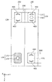
次に、蓄電素子100の構成について、詳細に説明する。図2は、本実施の形態に係る蓄電素子100の外観を示す斜視図及び断面図である。具体的には、図2の(a)は、蓄電素子100の外観を示す斜視図である。また、図2の(b)は、蓄電素子100の正極端子120をIIb-IIb断面で切断した場合の構成を拡大して示す拡大断面図である。さらに、図2の(c)は、蓄電素子100の負極端子130をIIc-IIc断面で切断した場合の構成を拡大して示す拡大断面図である。また、図3は、本実施の形態に係る蓄電素子100を分解して各構成要素を示す分解斜視図である。
[2 Description of the configuration of the storage element 100]
Next, the configuration of the
図2に示すように、蓄電素子100は、容器本体111及び蓋体112を有する容器110と、正極端子120と、負極端子130とを備えている。また、図3に示すように、容器110の内方には、電極体140と、正極集電体150と、負極集電体160とが収容されている。
As shown in FIG. 2 , the
なお、蓋体112と正極端子120との間、及び蓋体112と正極集電体150との間には、絶縁性及び気密性を高めるためにガスケット等が配置されているが、同図では省略して図示している。負極側についても、同様である。また、容器110の内部には、電解液(非水電解質)が封入されているが、図示は省略する。なお、当該電解液としては、蓄電素子100の性能を損なうものでなければその種類に特に制限はなく、様々なものを選択することができる。また、上記の構成要素の他、正極集電体150及び負極集電体160の側方に配置されるスペーサ、または、電極体140等を包み込む絶縁フィルムなどが配置されていてもよい。
Gaskets or the like are arranged between the
容器110は、矩形筒状で底を備える容器本体111と、容器本体111の開口を閉塞する板状部材である蓋体112とで構成されている。また、容器110は、電極体140等を内部に収容後、容器本体111と蓋体112とが溶接等されることにより、内部を密封することができる構成となっている。なお、容器本体111及び蓋体112の材質は特に限定されず、例えばステンレス鋼、アルミニウム、アルミニウム合金、鉄、メッキ鋼板など溶接可能な金属とすることができるが、樹脂を用いることもできる。また、蓋体112には、容器110内の圧力が上昇したときに当該圧力を開放するためのガス排出弁113、及び、容器110内に電解液を注液するための注液部114が設けられている。
The
電極体140は、正極板と負極板とセパレータとが積層されて形成された蓄電要素(発電要素)である。ここで、電極体が有する正極板は、アルミニウムまたはアルミニウム合金などの金属からなる長尺帯状の集電箔である正極基材層上に正極活物質層が形成されたものである。また、負極板は、銅または銅合金などの金属からなる長尺帯状の集電箔である負極基材層上に負極活物質層が形成されたものである。また、正極活物質層に用いられる正極活物質、負極活物質層に用いられる負極活物質としては、リチウムイオンを吸蔵放出可能なものであれば、適宜公知の材料を使用できる。なお、本実施の形態では、電極体140の断面形状として長円形状を図示しているが、円形状または楕円形状等でもよい。また、本実施の形態では、電極体140は、正極板と負極板とセパレータとが巻回されて形成された巻回型形状を図示しているが、平板状極板を積層した積層型形状や、長尺の平板状極板を折り畳んだ蛇腹状(つづら型)の形状等であることにしてもよい。
The
正極集電体150は、正極端子120と電極体140の端部141の正極板とに電気的に接続される導電性と剛性とを備えた部材である。また、負極集電体160は、負極端子130と電極体140の端部142の負極板とに電気的に接続される導電性と剛性とを備えた部材である。具体的には、正極集電体150及び負極集電体160は、容器本体111の側壁から蓋体112に沿って屈曲状態で配置される板状部材であり、蓋体112に固定的に接続(接合)されている。これにより、電極体140が、正極集電体150及び負極集電体160によって蓋体112から吊り下げられた状態で保持(支持)され、振動や衝撃などによる揺れが抑制される。なお、正極集電体150の材質は限定されないが、例えば、電極体140の正極基材層と同様、アルミニウムまたはアルミニウム合金などの金属で形成されている。また、負極集電体160についても、材質は限定されないが、例えば、電極体140の負極基材層と同様、銅または銅合金などの金属で形成されている。
The positive electrode
正極端子120は、電極体140の正極板に電気的に接続された電極端子であり、負極端子130は、電極体140の負極板に電気的に接続された電極端子である。つまり、正極端子120及び負極端子130は、電極体140に蓄えられている電気を蓄電素子100の外部空間に導出し、また、電極体140に電気を蓄えるために蓄電素子100の内部空間に電気を導入するための金属製の電極端子である。また、正極端子120及び負極端子130は、電極体140の上方に配置された蓋体112に取り付けられている。ここで、正極端子120及び負極端子130の構成について、さらに詳細に説明する。
The
[2.1 正極端子120の構成の説明]
まず、正極端子120の構成について、詳細に説明する。図3に示すように、正極端子120は、端子本体121と、軸部122とを有している。端子本体121は、正極端子120の本体部であり、XY平面に平行な矩形状かつ平板状の部位である。軸部122は、端子本体121の略中央位置からZ軸方向マイナス側に延設された円柱状の部位であり、蓋体112の貫通孔115と正極集電体150の貫通孔151とに挿入されて、蓋体112と正極集電体150とを貫通する。そして、軸部122のZ軸方向マイナス側の端部がかしめられることにより、正極端子120が、正極集電体150とともに蓋体112に固定される。
[2.1 Description of Configuration of Positive Electrode Terminal 120]
First, the configuration of the
ここで、端子本体121と軸部122とは、一体に形成されている。つまり、1つの部材が加工されて端子本体121及び軸部122が成形されることにより、正極端子120が形成されている。なお、正極端子120(端子本体121及び軸部122)の材質は限定されないが、例えば、電極体140の正極基材層と同様、アルミニウムまたはアルミニウム合金などの金属で形成されている。
Here, the terminal
また、図2の(b)に示すように、正極端子120の端子本体121は、容器110とは反対側(Z軸方向プラス側)の面である端子表面121aを有している。つまり、端子本体121は、蓋体112に対向する端子裏面(図示せず)と、当該端子裏面の反対側の面である端子表面121aとを有している。なお、軸部122は、容器110の内部に埋設されているため、端子表面121aは、正極端子120のうちの、容器110の内部に埋設される部位の反対側の面と定義することもできる。
As shown in FIG. 2B, the
また、端子表面121aは、上述の通り、バスバー200と接合される面であり、端子表面121aのバスバー200との接合領域には、複数の凸部121bが面状に配置されている。ここで、端子表面121aのバスバー200との接合領域とは、端子表面121aのうちのバスバー200との接合対象となる領域であり、本実施の形態では、端子表面121aの全面である。つまり、当該複数の凸部121bは、端子本体121の端子表面121aの全面に配置されている。具体的には、当該複数の凸部121bは、端子表面121aにおいてX軸方向及びY軸方向に略等間隔で配列されており、これにより、端子表面121aの全面に亘って凹凸が広がる形状となっている。つまり、端子表面121aには、蓄電素子100の他の面(例えば容器110の外面)よりも粗い凹凸が形成されている。
As described above, the
また、上記の接合領域は、蓄電素子100の電気特性を検査する際に、後述のプローブ21(図4参照)が接触する領域でもある。つまり、端子表面121aのうちのプローブ21が接触する領域において、複数の凸部121bが面状に配置されている。
In addition, the junction region is also a region with which a probe 21 (see FIG. 4), which will be described later, comes into contact when inspecting the electrical characteristics of the
なお、接合領域の全面がバスバー200と接合される必要はなく、また、接合領域は、端子表面121aの全面ではなく一部の面であってもよい。また、当該複数の凸部121bは、接合領域の全面ではなく一部の面に配置されていてもよい。言い換えれば、当該複数の凸部121bは、端子表面121aの全面ではなく一部の面に配置されていてもよい。つまり、端子表面121aにおいて、実際にバスバー200との接合が行われる箇所と、凸部121bが配置されている箇所とは、一致しない場合もある。例えば、接合領域内の凸部121bが配置されている箇所で、必ずしもバスバー200との接合が行われなくてもよく、また、接合領域内のバスバー200との接合が行われた箇所に、必ずしも凸部121bが配置されていなくてもよい。同様に、凸部121bが配置されている箇所の中には、プローブ21が接触しない箇所があってもよく、また、接合領域内のプローブ21が接触する領域の全てに、凸部121bが配置されていなくてもよい。
It should be noted that the entire bonding area need not be bonded to
ここで、端子表面121aに設けられた複数の凸部121bのそれぞれは、突出高さが0.05mm以上であるのが好ましく、0.1mm以上であるのがより好ましく、0.2mm以上であるのがさらに好ましい。また、当該複数の凸部121bのそれぞれは、突出高さが1mm以下であるのが好ましく、0.5mm以下であるのがより好ましく、0.3mm以下であるのがさらに好ましい。凸部121bの突出高さが小さ過ぎたり大き過ぎたりすると、凸部121bによる効果を十分に発揮することができないためである。
Here, each of the plurality of
また、当該複数の凸部121bのそれぞれは、先端部分が曲面形状を有している。つまり、凸部121bは、先端部分の断面形状における外縁が、曲線で形成されている。具体的には、凸部121bは、先端部分が、Z軸方向プラス側に向かうほど断面積が小さくなる形状を有している。このように、端子表面121aは、先端部分が先細り(錐体状)の複数の凸部121bが形成された剣山のような形状を有している。なお、凸部121bの先端部分の形状は、上述のような錐体状であるのが好ましいが、例えば柱体状等であってもかまわない。
Further, each of the plurality of
[2.2 負極端子130の構成の説明]
次に、負極端子130の構成について、詳細に説明する。図3に示すように、負極端子130は、端子本体131と、軸部132とを有している。端子本体131は、負極端子130の本体部であり、XY平面に平行な矩形状かつ平板状の部材である。軸部132は、端子本体131の略中央位置からZ軸方向マイナス側に延設された円柱状の部材であり、蓋体112の貫通孔116と負極集電体160の貫通孔161とに挿入されて、蓋体112と負極集電体160とを貫通する。そして、軸部132のZ軸方向マイナス側の端部がかしめられることにより、負極端子130が、負極集電体160とともに蓋体112に固定される。
[2.2 Description of Configuration of Negative Terminal 130]
Next, the configuration of the
ここで、端子本体131と軸部132とは、別体で構成されている。つまり、別体の端子本体131と軸部132とが圧入やかしめ等で接合されることにより、負極端子130が形成されている。このため、負極端子130の表面(Z軸方向プラス側の面、後述の表面130a)からは、軸部132の表面(Z軸方向プラス側の面、後述の軸部表面132a)が露出している。なお、負極端子130の材質は限定されないが、例えば、軸部122は、電極体140の負極基材層と同様、銅または銅合金などの金属で形成され、端子本体131は、アルミニウムまたはアルミニウム合金などの金属で形成されている。
Here, the terminal
また、図2の(c)に示すように、負極端子130の端子本体131は、容器110とは反対側(Z軸方向プラス側)の面である端子表面131aを有している。また、軸部132は、容器110とは反対側(Z軸方向プラス側)の面である軸部表面132aを有している。つまり、負極端子130は、Z軸方向プラス側に、端子表面131a及び軸部表面132aからなる表面130aを有しており、この表面130aが、正極端子120の端子本体121の端子表面121aに対応している。
Further, as shown in FIG. 2C, the
ここで、端子表面131aは、端子表面121aと同様に、バスバー200と接合される面であり、端子表面131aのバスバー200との接合領域には、複数の凸部131bが面状に配置されている。この接合領域は、正極側の端子表面121aの接合領域と同様に、端子表面131aのうちのバスバー200との接合対象となる領域であり、本実施の形態では、端子表面131aの全面である。つまり、当該複数の凸部131bは、端子本体131の端子表面131aの全面に配置されている。ただし、負極端子130においては、正極端子120とは異なり、軸部表面132aが端子表面131aから露出しているため、接合領域は、表面130aのうちの軸部表面132a以外の環状の領域(中空の領域、図2のドットで表示した部分)となる。このため、凸部131bも、表面130aのうちの軸部表面132a以外の当該環状の領域に形成されている。つまり、凸部131bは、端子表面131aの全面に形成され、かつ、軸部表面132aには形成されていない。
Here, the
また、当該接合領域は、蓄電素子100の電気特性を検査する際に、後述のプローブ22(図4参照)が接触する領域でもある。つまり、端子表面131aのうちのプローブ22が接触する領域において、複数の凸部131bが面状に配置されている。なお、接合領域と、バスバー200が実際に接合される箇所と、凸部131bが配置される箇所と、プローブ22が接触する箇所との関係については、上述の正極側と同様であるため、詳細な説明は省略する。また、凸部131bの突出高さ及び先端部分の形状についても、凸部121bの場合と同様であるため、詳細な説明は省略する。
The junction region is also a region with which a probe 22 (see FIG. 4), which will be described later, comes into contact when inspecting the electrical characteristics of the
[3 蓄電装置10の製造方法の説明]
次に、蓄電装置10の製造方法について、詳細に説明する。図4は、本実施の形態に係る蓄電装置10の製造方法のうちの蓄電素子100の検査方法における検査工程を説明する図である。具体的には、図4の(a)~(c)は、図2の(a)~(c)に対応しており、図2の(a)~(c)の蓄電素子100の正極端子120及び負極端子130に、プローブ21及び22を配置した状態を示している。また、図5は、本実施の形態に係る蓄電装置10の製造方法のうちの蓄電素子100とバスバー200との接合工程を説明する図である。具体的には、図5は、検査工程の後に、蓄電素子100の正極端子120及び負極端子130に、バスバー200を接合した状態を示している。
[3 Description of Method for Manufacturing Power Storage Device 10]
Next, a method for manufacturing
蓄電装置10の製造方法においては、まず、複数の凸部121b及び131bが面状に形成された正極端子120及び負極端子130を備える蓄電素子100を準備する。具体的には、正極端子120の端子表面121a、及び、負極端子130の端子表面131aにおけるバスバー200との溶接領域に、複数の凸部121b及び131bを面状に形成する。そして、正極端子120及び負極端子130を組み付けて、蓄電素子100を作製する。
In the method for manufacturing the
次に、蓄電素子100の電気特性を検査する。ここで、蓄電素子100の電気特性の検査とは、例えば、蓄電素子100の容量を確認したり、蓄電素子100の電圧や内部抵抗等を計測したり、電解液の未注液時に絶縁抵抗を計測したりする等、蓄電素子100に関する各種検査を含む。
Next, the electrical characteristics of the
具体的には、図4に示すように、蓄電素子100の検査方法における検査工程として、複数の凸部が面状に形成された電極端子の端子表面に、プローブを接触させて、蓄電素子100の電気特性を検査する。つまり、複数の凸部121bが面状に形成された正極端子120の端子表面121aにプローブ21を接触させ、かつ、複数の凸部131bが面状に形成された負極端子130の端子表面131aにプローブ22を接触させて、蓄電素子100の電気特性を検査する。
Specifically, as shown in FIG. 4, as an inspection step in an inspection method of the
ここで、プローブ21、22は、蓄電素子100の電気特性の検査用のプローブであり、本実施の形態では、端子表面121a、131aとの接触面(先端面、Z軸方向マイナス側の面)が、平坦に形成されている。このため、このプローブ21、22の端子表面121a、131aとの接触面を、平坦面21a、22aと呼ぶ。つまり、上記検査工程では、端子表面121a、131aに、プローブ21、22の平坦面21a、22aを接触させて、蓄電素子100の電気特性を検査する。
Here, the
また、プローブ21、22は、端子表面121a、131aよりも硬度が高い部材で形成されている。例えば、端子表面121a、131aがアルミニウムで形成されている場合には、プローブ21、22は、アルミニウムよりも硬い材質で形成されている。プローブ21、22は、例えば、鋼(工具鋼)で形成され、より具体的には、炭素工具鋼(SK材)に金メッキが施されたものが用いられる。つまり、上記検査工程では、端子表面121a、131aに、端子表面121a、131aよりも硬度が高いプローブ21、22を接触させて、蓄電素子100の電気特性を検査する。
Moreover, the
ここで、図4の(a)及び(c)に示すように、負極端子130においては、軸部表面132aを避けるように、例えば、軸部表面132aよりもX軸方向マイナス側の端子表面131aにプローブ22を接触させる。正極端子120については、端子表面121aのどの位置にプローブ21を接触させてもよいが、負極端子130と位置を対応させて、端子表面121aのX軸方向プラス側の面にプローブ21を接触させる。この際、例えば端子表面121aが少し変形していたり傾いたりしているような場合には、端子表面121aにプローブ21を押し付けて、凸部121bを圧縮する(つぶす)ことで、端子表面121aとプローブ21との接触不良を抑制することができる。なお、プローブ21、22は、端子表面121a、131aの傾きに追従できるように、フレキシブルに可動できる構成を有していてもよい。
Here, as shown in FIGS. 4A and 4C, in the
そして、上記検査工程の後、図5に示すように、蓄電素子100とバスバー200とを接合する。具体的には、正極端子120の端子表面121aの接合領域、及び、負極端子130の端子表面131aの接合領域に、バスバー200を接合する。さらに具体的には、バスバー200の、端子表面121a及び131aの接合領域に対応する位置に、例えばレーザ光を照射することで、正極端子120及び負極端子130とバスバー200とが接合(レーザ溶接)された接合部400が形成される。接合部400は、正極端子120及び負極端子130のX軸方向プラス側及びマイナス側の部位とバスバー200とが接合された上面視円弧形状の接合部である。なお、接合部400の位置及び形状は、特に限定されない。
Then, after the inspection process, as shown in FIG. 5, the
これにより、正極端子120及び負極端子130とバスバー200とが、端子表面121a及び131aに形成された凸部121b及び131bの位置で接合(溶接)される。この際、例えば端子表面121aが少し変形していたり傾いたりしているような場合には、端子表面121aにバスバー200を押し付けて、凸部121bを圧縮する(つぶす)ことで、端子表面121aとバスバー200との接合不良(溶接不良)を抑制することができる。
Thereby, the
また、溶接時に多少のクリアランスがある方が、当該クリアランスに溶接部が入り込み、溶接部が広がるため、溶接幅が増加すると考えられる。また、溶接によって発生するガスが当該クリアランスから排出されるため、これによっても溶接幅を増加させることができると考えられる。溶接幅が大きいと、溶接強度が高くなるため好ましい。ただし、当該クリアランスが小さ過ぎると、当該クリアランスに溶接部が十分に入り込み難いため溶接幅を増加することができず、当該クリアランスが大きくなり過ぎると、当該クリアランスに入り込む溶接部の量が足りなくなり溶接幅が小さくなってしまう。このため、当該クリアランスが、0.05mm以上かつ0.25mm以下であるのが好ましく、0.1mm以上かつ0.2mm以下であるのがさらに好ましい。つまり、凸部121b及び131bは、溶接時には、突出高さが、50μm以上かつ250μm以下になっているのが好ましく、100μm以上かつ200μm以下になっているのがさらに好ましい。
In addition, it is thought that if there is a certain amount of clearance during welding, the welded portion will enter the clearance and the welded portion will widen, resulting in an increase in the weld width. In addition, since the gas generated by welding is discharged from the clearance, it is considered that the welding width can also be increased. A large weld width is preferable because the weld strength increases. However, if the clearance is too small, the weld width cannot be increased because it is difficult for the weld to enter the clearance sufficiently. width becomes smaller. Therefore, the clearance is preferably 0.05 mm or more and 0.25 mm or less, and more preferably 0.1 mm or more and 0.2 mm or less. In other words, the
また、接合部400においては、溶接によって凸部121b及び131bの形状は変化しているが、接合部400の周囲に凸部121bまたは131bが形成されていることを確認する等により、接合部400の位置に凸部121bまたは131bが形成されていたことを推認することができる。なお、接合領域における接合は、レーザ溶接には限定されず、例えば、抵抗溶接、超音波接合、導電性の接着剤や両面テープ等による接着、熱溶着等による溶着、かしめ等による機械的な接合等、種々の接合手法を適用可能である。
In addition, although the shapes of the
[4 効果の説明]
以上のように、本発明の実施の形態に係る蓄電素子100の検査方法によれば、検査工程として、複数の凸部121b、131bが面状に形成された電極端子(正極端子120、負極端子130)の端子表面121a、131aに、プローブ21、22を接触させて、蓄電素子100の電気特性を検査する。このように、電極端子の端子表面121a、131aに複数の凸部121b、131bが面状に形成された蓄電素子100を用いて、当該電極端子の端子表面121a、131aにプローブ21、22を接触させることで、プローブ21、22と電極端子との接触不良を抑制することができる。つまり、蓄電素子100の電極端子に凸部121b、131bが設けられているため、同じプローブ21、22を用いて繰り返し検査を行った場合でも、プローブ21、22と電極端子との接触を確保できる状態を保つことができる。例えば、電極端子の端子表面121a、131aが傾いていたりしても、端子表面121a、131aの凸部121b、131bがつぶれたりすることで、電極端子とプローブ21、22との接触を確保することができる。これにより、プローブ21、22と電極端子とが接触不良を起こすのを抑制して蓄電素子100の電気特性を検査することができるため、電気特性の検査精度が低下するのを抑制することができる。
[4 Explanation of effects]
As described above, according to the inspection method of the
また、上記検査工程では、複数の凸部121b、131bが面状に形成された電極端子の端子表面121a、131aに、プローブ21、22の平坦面21a、22aを接触させて、蓄電素子100の電気特性を検査する。このように、プローブ21、22の電極端子との当接面が平坦面であるため、同じプローブ21、22を用いて繰り返し検査を行った場合でも、電極端子の材料がプローブ21、22に付着するのを抑制し、プローブ21、22と電極端子との接触を確保できる状態を保つことができる。これにより、プローブ21、22と電極端子とが接触不良を起こすのを抑制して蓄電素子100の電気特性を検査することができるため、電気特性の検査精度が低下するのを抑制することができる。
In the inspection process, the
また、上記検査工程では、複数の凸部121b、131bが面状に形成された電極端子の端子表面121a、131aに、端子表面121a、131aよりも硬度が高いプローブ21、22を接触させて、蓄電素子100の電気特性を検査する。このように、プローブ21、22が電極端子の端子表面121a、131aよりも硬いため、プローブ21、22を端子表面121a、131aに接触させることで、端子表面121a、131aの複数の凸部121b、131bがつぶれ、プローブ21、22と電極端子との接触を確保することができる。これにより、プローブ21、22と電極端子とが接触不良を起こすのを抑制して蓄電素子100の電気特性を検査することができるため、電気特性の検査精度が低下するのを抑制することができる。
Further, in the inspection process, the
また、本発明の実施の形態に係る蓄電素子100によれば、電極端子(正極端子120、負極端子130)は、容器110とは反対側に端子表面121a、131aを有しており、端子表面121a、131aの他の部材(バスバー200等)との接合領域には、複数の凸部121b、131bが面状に配置されている。ここで、電極端子の端子表面121a、131aにプローブ21、22を接触させて検査を行う場合には、スペース上の問題から、端子表面121a、131aにおける当該接合領域にプローブ21、22を接触させることとなる。このため、端子表面121a、131aの面状に形成された複数の凸部121b、131bにプローブ21、22を接触させることとなり、プローブ21、22と電極端子との接触不良を抑制することができる。また、端子表面121a、131aは、電極端子の容器110とは反対側の面であるため、プローブ21、22を端子表面121a、131aに接触させる際に、容器110が土台となって、電極端子を安定して支持することができ、端子表面121a、131aが撓んだり傾いたりするのを抑制することができる。これにより、プローブ21、22と電極端子とが接触不良を起こすのを抑制して蓄電素子100の電気特性を検査することができるため、電気特性の検査精度が低下するのを抑制することができる。
Further, according to the
また、電極端子の端子表面121a、131aに他の部材(バスバー200等)を接合する場合においても、複数の凸部121b、131bが面状に配置された接合領域に当該他の部材を接触させることで、電極端子と当該他の部材との接触不良を抑制することができる。例えば、電極端子の端子表面121a、131aが傾いていたりしても、端子表面121a、131aの凸部121b、131bがつぶれたりすることで、電極端子と当該他の部材との接触を確保することができる。また、端子表面121a、131aは、電極端子の容器110とは反対側の面であるため、当該他の部材を端子表面121a、131aに接合する際に、容器110が土台となって、電極端子を安定して支持することができ、端子表面121a、131aが撓んだり傾いたりするのを抑制することができる。これにより、電極端子と当該他の部材とが接合不良を起こすのを抑制することができるため、電極端子と当該他の部材との接合強度を向上させることができる。また、電極端子と当該他の部材とを溶接により接合する場合には、端子表面121a、131aの凸部121b、131bの部分で局所的に急加熱されるため、電極端子と当該他の部材との接合強度をさらに向上させることができる。
Also, when bonding other members (such as the bus bar 200) to the
また、蓄電素子100において、電極端子の端子表面121a、131aに配置された複数の凸部121b、131bのそれぞれは、突出高さが0.1mm以上であるのが好ましい。このように、凸部121b、131bが0.1mm以上の高さを有することで、電極端子の端子表面121a、131aにプローブ21、22を接触させて検査を行う際に、凸部121b、131bがつぶれてプローブ21、22と電極端子とを接触しやすくすることができる。これにより、プローブ21、22と電極端子とが接触不良を起こすのを抑制して蓄電素子100の電気特性を検査することができるため、電気特性の検査精度が低下するのを抑制することができる。
Moreover, in the
また、電極端子の端子表面121a、131aの凸部121b、131bが0.1mm以上の高さを有することで、凸部121b、131bがつぶれて電極端子と他の部材(バスバー200等)とを接触しやすくすることができる。これにより、電極端子と当該他の部材とが接合不良を起こすのを抑制することができるため、電極端子と当該他の部材との接合強度を向上させることができる。
In addition, since the
また、蓄電素子100において、電極端子の端子表面121a、131aに配置された複数の凸部121b、131bのそれぞれは、先端部分が曲面形状を有している。このように、凸部121b、131bの先端部分が曲面形状を有している(尖っていない)ことで、電極端子の端子表面121a、131aにプローブ21、22を接触させて検査を行う際に、電極端子の凸部121b、131bの先端の部材がプローブ21、22に付着するのを抑制することができる。これにより、プローブ21、22と電極端子とが接触不良を起こすのを抑制して蓄電素子100の電気特性を検査することができるため、電気特性の検査精度が低下するのを抑制することができる。
Further, in the
また、電極端子の端子表面121a、131aの凸部121b、131bの先端部分が曲面形状を有している(尖っていない)ことで、電極端子と他の部材(バスバー200等)との接触面積をある程度確保することができる。これにより、電極端子と当該他の部材とが接合不良を起こすのを抑制することができるため、電極端子と当該他の部材との接合強度を向上させることができる。
In addition, since the tip portions of the
また、蓄電素子100において、複数の凸部121b、131bは、電極端子の端子本体121、131の端子表面121a、131aの全面に配置されている。このように、凸部121b、131bを端子表面121a、131aの全面に配置することで、凸部121b、131bの形成位置を位置決めする必要がないため、端子表面121a、131aに容易に凸部121b、131bを形成することができる。また、プローブ21、22を端子表面121a、131aのどこに配置してもよいため、プローブ21、22を容易に位置決めして検査を行うことができる。これにより、プローブ21、22と電極端子とが接触不良を起こすのを抑制して蓄電素子100の電気特性を検査することができるため、電気特性の検査精度が低下するのを抑制することができる。
Moreover, in the
また、凸部121b、131bを端子表面121a、131aの全面に配置することで、端子表面121a、131aに他の部材(バスバー200等)を接合する際に、端子表面121a、131aへの当該他の部材の位置決め精度を高くする必要がない。これにより、電極端子と当該他の部材とが接合不良を起こすのを抑制することができるため、電極端子と当該他の部材との接合強度を向上させることができる。
In addition, by arranging the
[5 変形例の説明]
以上、本発明の実施の形態に係る蓄電装置及び蓄電素子、並びに、その製造方法及び検査方法について説明したが、本発明は、この実施の形態に限定されるものではない。つまり、今回開示された実施の形態は全ての点で例示であって制限的なものではないと考えられるべきである。本発明の範囲は上記した説明ではなくて特許請求の範囲によって示され、特許請求の範囲と均等の意味及び範囲内での全ての変更が含まれることが意図される。
[5 Description of Modifications]
Although the power storage device and power storage element according to the embodiment of the present invention, and the manufacturing method and inspection method thereof have been described above, the present invention is not limited to this embodiment. In other words, it should be considered that the embodiments disclosed this time are illustrative in all respects and not restrictive. The scope of the present invention is indicated by the scope of the claims rather than the above description, and is intended to include all modifications within the scope and meaning equivalent to the scope of the claims.
例えば、上記実施の形態では、プローブ21、22は、先端面として平坦面21a、22aを有していることとした。しかし、プローブ21、22は、曲面形状や凹凸が形成された先端面を有していることにしてもよい。
For example, in the above embodiments, the
また、上記実施の形態では、プローブ21、22は、端子表面121a、131aよりも硬度が高い部材で形成されていることとした。しかし、プローブ21、22は、端子表面121a、131aと同等、または、端子表面121a、131aよりも少し硬度が低い部材で形成されていることにしてもよい。この場合でも、プローブ21、22を、端子表面121a、131aに面状に形成された複数の凸部121b、131bに接触させることで、プローブ21、22と電極端子との接触不良を抑制する効果を多少は発揮することができる。
Moreover, in the above-described embodiment, the
また、上記実施の形態では、検査工程に用いられる蓄電素子100は、容器110とは反対側の面に、端子表面121a、131aを有していることとした。しかし、当該蓄電素子100の端子表面121a、131aは、容器110とは反対側の面ではなく、例えば、当該反対側の面に隣接する面に配置されていることにしてもよい。
Further, in the above-described embodiment, the
また、上記実施の形態では、検査工程において、端子表面121a、131aの他の部材との接合領域内の凸部121b、131bに、プローブ21、22が接触することとした。しかし、端子表面121a、131aの当該接合領域以外に凸部121b、131bが設けられており、この凸部121b、131bに、プローブ21、22が接触することにしてもよい。
In the above embodiment, in the inspection process, the
また、上記実施の形態では、端子表面121a、131aと接合される他の部材は、バスバー200であることとした。しかし、当該他の部材は、例えば、蓄電素子100の電極端子と蓄電装置10の外部接続端子とを繋ぐバスバーであることにしてもよいし、その他、端子表面121a、131aと接合される部材であれば、どのような部材であってもよい。
Further, in the above-described embodiment, another member that is joined to
また、上記実施の形態では、凸部121b、131bは、端子本体121、131に一体に形成されていることとした。しかし、凸部121b、131bは、端子本体121、131とは別体に構成されて、端子本体121、131に接合されていることにしてもよい。
Further, in the above-described embodiment, the
また、上記実施の形態では、負極端子130において、軸部表面132aには凸部は形成されていないこととした。しかし、軸部表面132aにも凸部が形成されていることにしてもよい。
Further, in the above-described embodiment, in the
また、上記実施の形態では、全ての蓄電素子100が上記の構成を有していることとしたが、いずれかの蓄電素子100が上記の構成を有していないことにしてもよい。また、蓄電素子100において、正極側及び負極側の双方が上記の構成を有していることとしたが、正極側及び負極側のいずれか一方しか上記の構成を有していないことにしてもよい。
Further, in the above embodiment, all the
また、上記実施の形態及び上記変形例を任意に組み合わせて構築される形態も、本発明の範囲内に含まれる。 Moreover, the form constructed by arbitrarily combining the above embodiment and the above modifications is also included in the scope of the present invention.
また、本発明は、このような蓄電素子100として実現することができるだけでなく、蓄電素子100が備える電極端子(正極端子120、負極端子130)としても実現することができる。
In addition, the present invention can be realized not only as the
本発明は、リチウムイオン二次電池などの蓄電素子の検査方法等に適用できる。 INDUSTRIAL APPLICABILITY The present invention can be applied to a method for inspecting an electric storage element such as a lithium ion secondary battery.
10 蓄電装置
21、22 プローブ
21a、22a 平坦面
100 蓄電素子
110 容器
111 容器本体
112 蓋体
113 ガス排出弁
114 注液部
115、116、151、161 貫通孔
120 正極端子
121、131 端子本体
121a、131a 端子表面
121b、131b 凸部
122、132 軸部
130 負極端子
130a 表面
132a 軸部表面
140 電極体
141、142 端部
150 正極集電体
160 負極集電体
200 バスバー
300 外装体
400 接合部
10
Claims (6)
複数の凸部が面状に形成された前記電極端子の端子表面に、プローブを接触させて、前記蓄電素子の電気特性を検査する検査工程を含み、
前記検査工程では、前記端子表面に、前記プローブの平坦面を接触させて、前記蓄電素子の電気特性を検査する
蓄電素子の検査方法。 A method for inspecting a storage element having an electrode terminal, comprising:
an inspection step of inspecting electrical characteristics of the electric storage element by bringing a probe into contact with a terminal surface of the electrode terminal having a plurality of planar projections ;
In the inspection step, a flat surface of the probe is brought into contact with the surface of the terminal to inspect electrical characteristics of the storage element.
A method for inspecting a power storage element.
請求項1に記載の蓄電素子の検査方法。 2. The method of inspecting an electric storage element according to claim 1 , wherein, in the inspection step, the electric characteristics of the electric storage element are inspected by contacting the terminal surface with the probe having a hardness higher than that of the terminal surface.
前記電極端子は、前記容器とは反対側の面であって他の部材と接合される端子表面を有し、
前記端子表面の前記他の部材との接合領域には、複数の凸部が面状に配置され、
前記電極端子は、前記端子表面を有する端子本体と、前記蓄電素子の容器を貫通する軸部とを有し、
前記複数の凸部は、前記端子本体の端子表面の全面に配置されている
蓄電素子。 A storage element comprising a container and an electrode terminal,
The electrode terminal has a terminal surface on the opposite side of the container and to be joined to another member,
a plurality of projections are arranged in a planar manner in the joint region with the other member on the surface of the terminal ;
The electrode terminal has a terminal body having the terminal surface and a shaft penetrating the container of the storage element,
The plurality of protrusions are arranged over the entire terminal surface of the terminal body.
storage device.
前記電極端子は、前記容器とは反対側の面である端子表面を有し、
前記端子表面には、複数の凸部が面状に配置され、
前記複数の凸部のそれぞれは、突出高さが0.05mm以上である
蓄電素子。 A storage element comprising a container and an electrode terminal,
The electrode terminal has a terminal surface opposite to the container,
A plurality of projections are arranged in a plane on the surface of the terminal ,
Each of the plurality of protrusions has a protrusion height of 0.05 mm or more.
storage device.
請求項3または4に記載の蓄電素子。 The electric storage device according to claim 3 or 4, wherein each of the plurality of protrusions has a protrusion height of 0.1 mm or more.
請求項3~5のいずれか1項に記載の蓄電素子。 The power storage device according to any one of claims 3 to 5, wherein each of the plurality of projections has a curved tip portion.
Priority Applications (1)
| Application Number | Priority Date | Filing Date | Title |
|---|---|---|---|
| JP2018060565A JP7151123B2 (en) | 2018-03-27 | 2018-03-27 | Electric storage element inspection method and electric storage element |
Applications Claiming Priority (1)
| Application Number | Priority Date | Filing Date | Title |
|---|---|---|---|
| JP2018060565A JP7151123B2 (en) | 2018-03-27 | 2018-03-27 | Electric storage element inspection method and electric storage element |
Publications (2)
| Publication Number | Publication Date |
|---|---|
| JP2019175618A JP2019175618A (en) | 2019-10-10 |
| JP7151123B2 true JP7151123B2 (en) | 2022-10-12 |
Family
ID=68167267
Family Applications (1)
| Application Number | Title | Priority Date | Filing Date |
|---|---|---|---|
| JP2018060565A Active JP7151123B2 (en) | 2018-03-27 | 2018-03-27 | Electric storage element inspection method and electric storage element |
Country Status (1)
| Country | Link |
|---|---|
| JP (1) | JP7151123B2 (en) |
Families Citing this family (2)
| Publication number | Priority date | Publication date | Assignee | Title |
|---|---|---|---|---|
| JP7125444B2 (en) * | 2020-03-24 | 2022-08-24 | パナソニックホールディングス株式会社 | battery module |
| CN116014321A (en) * | 2023-02-09 | 2023-04-25 | 深圳海润新能源科技有限公司 | End cover assembly, energy storage device and electric equipment |
Citations (6)
| Publication number | Priority date | Publication date | Assignee | Title |
|---|---|---|---|---|
| JP2003329706A (en) | 2002-05-10 | 2003-11-19 | Hitachi Maxell Ltd | Contact terminal for measuring electrical characteristics, apparatus for measuring electrical characteristics and apparatus for manufacturing battery |
| JP2008053485A (en) | 2006-08-25 | 2008-03-06 | Tdk Corp | Ptc element, and battery protection system |
| JP2008251453A (en) | 2007-03-30 | 2008-10-16 | Fdk Energy Co Ltd | Metal component for battery, its manufacturing method, and battery |
| WO2012073331A1 (en) | 2010-11-30 | 2012-06-07 | 日立ビークルエナジー株式会社 | Rechargeable battery and rechargeable battery module |
| JP2014135203A (en) | 2013-01-10 | 2014-07-24 | Hitachi Vehicle Energy Ltd | Square secondary battery |
| JP2015072746A (en) | 2013-10-01 | 2015-04-16 | トヨタ自動車株式会社 | Method of manufacturing battery |
-
2018
- 2018-03-27 JP JP2018060565A patent/JP7151123B2/en active Active
Patent Citations (6)
| Publication number | Priority date | Publication date | Assignee | Title |
|---|---|---|---|---|
| JP2003329706A (en) | 2002-05-10 | 2003-11-19 | Hitachi Maxell Ltd | Contact terminal for measuring electrical characteristics, apparatus for measuring electrical characteristics and apparatus for manufacturing battery |
| JP2008053485A (en) | 2006-08-25 | 2008-03-06 | Tdk Corp | Ptc element, and battery protection system |
| JP2008251453A (en) | 2007-03-30 | 2008-10-16 | Fdk Energy Co Ltd | Metal component for battery, its manufacturing method, and battery |
| WO2012073331A1 (en) | 2010-11-30 | 2012-06-07 | 日立ビークルエナジー株式会社 | Rechargeable battery and rechargeable battery module |
| JP2014135203A (en) | 2013-01-10 | 2014-07-24 | Hitachi Vehicle Energy Ltd | Square secondary battery |
| JP2015072746A (en) | 2013-10-01 | 2015-04-16 | トヨタ自動車株式会社 | Method of manufacturing battery |
Also Published As
| Publication number | Publication date |
|---|---|
| JP2019175618A (en) | 2019-10-10 |
Similar Documents
| Publication | Publication Date | Title |
|---|---|---|
| US9768425B2 (en) | Battery module | |
| JP5528746B2 (en) | Assembled battery | |
| WO2009128335A1 (en) | Battery and method for manufacturing the same | |
| KR101964760B1 (en) | Energy storage device and method of producing the same | |
| US20150214568A1 (en) | Manufacturing method of electric storage apparatus, auxiliary plate for ultrasonic welding, and electric storage apparatus | |
| KR102140311B1 (en) | Battery module, battery pack including the same, and vehicle including the same | |
| CN108063211B (en) | Power storage device and method for manufacturing power storage device | |
| US10763483B2 (en) | Battery pack | |
| JP2017112063A (en) | Bus bar module and method of manufacturing the same | |
| JP2016115601A (en) | Power storage module | |
| KR20160027193A (en) | Insertion guide device for film armored battery | |
| US10084163B2 (en) | Sealed battery manufacturing method | |
| JP7151123B2 (en) | Electric storage element inspection method and electric storage element | |
| US8765300B2 (en) | Battery manufacturing method, battery, pre-welding positive plate manufacturing method, and pre-welding positive plate | |
| US20150183052A1 (en) | Manufacturing method of electric storage apparatus and electric storage apparatus | |
| JP6947575B2 (en) | Manufacturing method of power storage element | |
| JP7023359B2 (en) | Battery pack | |
| US20220069400A1 (en) | Energy storage apparatus | |
| US20200176738A1 (en) | Energy storage apparatus | |
| JP6924366B2 (en) | Sealed battery | |
| JP5514618B2 (en) | Secondary battery | |
| US20220149474A1 (en) | Energy storage apparatus | |
| US20220094021A1 (en) | Energy storage apparatus | |
| CN114467159A (en) | Electricity storage device | |
| KR102641236B1 (en) | Terminal for secondary battery and secondary battery provided with the terminal |
Legal Events
| Date | Code | Title | Description |
|---|---|---|---|
| A621 | Written request for application examination |
Free format text: JAPANESE INTERMEDIATE CODE: A621 Effective date: 20210224 |
|
| A977 | Report on retrieval |
Free format text: JAPANESE INTERMEDIATE CODE: A971007 Effective date: 20220217 |
|
| A131 | Notification of reasons for refusal |
Free format text: JAPANESE INTERMEDIATE CODE: A131 Effective date: 20220315 |
|
| A521 | Request for written amendment filed |
Free format text: JAPANESE INTERMEDIATE CODE: A523 Effective date: 20220510 |
|
| TRDD | Decision of grant or rejection written | ||
| A01 | Written decision to grant a patent or to grant a registration (utility model) |
Free format text: JAPANESE INTERMEDIATE CODE: A01 Effective date: 20220830 |
|
| A61 | First payment of annual fees (during grant procedure) |
Free format text: JAPANESE INTERMEDIATE CODE: A61 Effective date: 20220912 |
|
| R150 | Certificate of patent or registration of utility model |
Ref document number: 7151123 Country of ref document: JP Free format text: JAPANESE INTERMEDIATE CODE: R150 |