JP7150223B2 - Phase shifter and phased array antenna device - Google Patents
Phase shifter and phased array antenna device Download PDFInfo
- Publication number
- JP7150223B2 JP7150223B2 JP2022543816A JP2022543816A JP7150223B2 JP 7150223 B2 JP7150223 B2 JP 7150223B2 JP 2022543816 A JP2022543816 A JP 2022543816A JP 2022543816 A JP2022543816 A JP 2022543816A JP 7150223 B2 JP7150223 B2 JP 7150223B2
- Authority
- JP
- Japan
- Prior art keywords
- capacitor
- inductor
- pass filter
- phase
- pass
- Prior art date
- Legal status (The legal status is an assumption and is not a legal conclusion. Google has not performed a legal analysis and makes no representation as to the accuracy of the status listed.)
- Active
Links
- 239000003990 capacitor Substances 0.000 claims description 165
- 230000010363 phase shift Effects 0.000 description 62
- 238000010586 diagram Methods 0.000 description 15
- 238000004088 simulation Methods 0.000 description 10
- 230000005540 biological transmission Effects 0.000 description 5
- 239000000470 constituent Substances 0.000 description 2
- SOBMVBSSEJZEBX-UHFFFAOYSA-N 2-[2,2-bis(2-octadecanoyloxyethoxymethyl)butoxy]ethyl octadecanoate Chemical compound CCCCCCCCCCCCCCCCCC(=O)OCCOCC(CC)(COCCOC(=O)CCCCCCCCCCCCCCCCC)COCCOC(=O)CCCCCCCCCCCCCCCCC SOBMVBSSEJZEBX-UHFFFAOYSA-N 0.000 description 1
- 230000004048 modification Effects 0.000 description 1
- 238000012986 modification Methods 0.000 description 1
- 230000007704 transition Effects 0.000 description 1
Images


Classifications
-
- H—ELECTRICITY
- H01—ELECTRIC ELEMENTS
- H01Q—ANTENNAS, i.e. RADIO AERIALS
- H01Q3/00—Arrangements for changing or varying the orientation or the shape of the directional pattern of the waves radiated from an antenna or antenna system
- H01Q3/24—Arrangements for changing or varying the orientation or the shape of the directional pattern of the waves radiated from an antenna or antenna system varying the orientation by switching energy from one active radiating element to another, e.g. for beam switching
-
- H—ELECTRICITY
- H01—ELECTRIC ELEMENTS
- H01P—WAVEGUIDES; RESONATORS, LINES, OR OTHER DEVICES OF THE WAVEGUIDE TYPE
- H01P1/00—Auxiliary devices
- H01P1/18—Phase-shifters
-
- H—ELECTRICITY
- H03—ELECTRONIC CIRCUITRY
- H03H—IMPEDANCE NETWORKS, e.g. RESONANT CIRCUITS; RESONATORS
- H03H7/00—Multiple-port networks comprising only passive electrical elements as network components
- H03H7/18—Networks for phase shifting
- H03H7/19—Two-port phase shifters providing a predetermined phase shift, e.g. "all-pass" filters
Landscapes
- Filters And Equalizers (AREA)
- Waveguide Switches, Polarizers, And Phase Shifters (AREA)
- Networks Using Active Elements (AREA)
Description
本開示は、移相器と、移相器を備えるフェーズドアレーアンテナ装置とに関するものである。 The present disclosure relates to a phase shifter and a phased array antenna apparatus comprising the phase shifter.
フェーズドアレーアンテナ装置には、一般的に、信号の位相を変化させることが可能な移相器が実装される。当該移相器は、フェーズドアレーアンテナ装置に含まれているアンテナ素子と接続される。
以下の非特許文献1には、第1の経路の通過位相と、第2の経路の通過位相との位相差が、移相量となる移相器が開示されている。第1の経路には、複数の第1の全域通過フィルタが直列に接続されている回路が挿入され、第2の経路には、複数の第2の全域通過フィルタが直列に接続されている回路が挿入されている。第1の全域通過フィルタは、集中定数素子として、2つのインダクタ及び2つのキャパシタを含んでいる。また、第2の全域通過フィルタは、集中定数素子として、2つのインダクタ及び2つのキャパシタを含んでいる。A phased array antenna apparatus is generally implemented with a phase shifter capable of changing the phase of the signal. The phase shifter is connected with the antenna elements included in the phased array antenna arrangement.
The following
非特許文献1に開示されている移相器では、移相量と整合条件とを実現する集中定数素子の組み合わせが一意に決定され、移相量の周波数特性も一意に決定される。このため、所望の周波数帯域において、移相誤差が一意に決定され、所望の移相量が得られないことがあるという課題があった。
In the phase shifter disclosed in
本開示は、上記のような課題を解決するためになされたもので、所望の周波数帯域において、所望の移相量の周波数特性を実現することができる移相器を得ることを目的とする。 The present disclosure has been made to solve the problems described above, and an object of the present disclosure is to obtain a phase shifter capable of realizing frequency characteristics with a desired amount of phase shift in a desired frequency band.
本開示に係る移相器は、複数の素子を含んでいる第1の全域通過フィルタと、複数の素子を含んでいる第2の全域通過フィルタと、第1の全域通過フィルタ、又は、第2の全域通過フィルタのいずれか一方に信号を与える第1の切替スイッチと、第1の全域通過フィルタを通過してきた信号、又は、第2の全域通過フィルタを通過してきた信号を選択する第2の切替スイッチとを備え、第1の全域通過フィルタは、複数の素子として、第1のインダクタ、第2のインダクタ、第1のキャパシタ、第2のキャパシタ及び第3のキャパシタを含んでおり、第2の全域通過フィルタは、複数の素子として、第3のインダクタ、第4のインダクタ、第4のキャパシタ、第5のキャパシタ及び第6のキャパシタを含んでおり、第1のインダクタは、第1の切替スイッチと第2の切替スイッチとを結ぶ第1の経路に挿入されており、第1のキャパシタの一端は、第1のインダクタの一端と接続されており、第2のキャパシタの一端は、第1のインダクタの他端と接続されており、第2のインダクタの一端は、第1のキャパシタ及び第2のキャパシタにおけるそれぞれの他端と接続されており、第3のキャパシタの一端は、第2のインダクタの他端と接続され、第3のキャパシタの他端は、接地されており、第3のインダクタは、第1の切替スイッチと第2の切替スイッチとを結ぶ第2の経路に挿入されており、第4のキャパシタの一端は、第3のインダクタの一端と接続されており、第5のキャパシタの一端は、第3のインダクタの他端と接続されており、第4のインダクタの一端は、第4のキャパシタ及び第5のキャパシタにおけるそれぞれの他端と接続されており、第6のキャパシタの一端は、第4のインダクタの他端と接続され、第6のキャパシタの他端は、接地されており、第1の全域通過フィルタに含まれている複数の素子の素子値及び第2の全域通過フィルタに含まれている複数の素子の素子値が、インピーダンス整合を実現するインピーダンス、信号の周波数及び変数によって決定されているものである。 A phase shifter according to the present disclosure includes a first allpass filter including a plurality of elements, a second allpass filter including a plurality of elements, the first allpass filter, or the second and a second switch for selecting the signal that has passed through the first all-pass filter or the signal that has passed through the second all-pass filter. a selector switch, the first all-pass filter including, as a plurality of elements, a first inductor, a second inductor, a first capacitor, a second capacitor, and a third capacitor; includes, as a plurality of elements, a third inductor, a fourth inductor, a fourth capacitor, a fifth capacitor, and a sixth capacitor, the first inductor being the first switching One end of the first capacitor is connected to one end of the first inductor, and one end of the second capacitor is connected to the first , one end of the second inductor is connected to the other ends of the first capacitor and the second capacitor, and one end of the third capacitor is connected to the second end of the second inductor. The other end of the third capacitor is connected to the other end of the inductor, the other end of the third capacitor is grounded, and the third inductor is inserted in the second path connecting the first switch and the second switch. , one end of the fourth capacitor is connected to one end of the third inductor, one end of the fifth capacitor is connected to the other end of the third inductor, and one end of the fourth inductor is connected to , the fourth capacitor and the fifth capacitor, one end of the sixth capacitor is connected to the other end of the fourth inductor, and the other end of the sixth capacitor is grounded. and the element values of the plurality of elements included in the first all-pass filter and the element values of the plurality of elements included in the second all-pass filter are the impedance and signal It is determined by frequency and variables.
本開示によれば、所望の周波数帯域において、所望の移相量の周波数特性を実現することができる。 According to the present disclosure, it is possible to achieve frequency characteristics with a desired phase shift amount in a desired frequency band.
以下、本開示をより詳細に説明するために、本開示を実施するための形態について、添付の図面に従って説明する。 Hereinafter, in order to describe the present disclosure in more detail, embodiments for carrying out the present disclosure will be described with reference to the accompanying drawings.
実施の形態1.
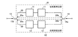
図1は、実施の形態1に係る移相器1を示す構成図である。
移相器1は、第1の全域通過フィルタ11、第2の全域通過フィルタ12、第1の切替スイッチ13及び第2の切替スイッチ14を備えている。
第1の全域通過フィルタ11は、複数の素子として、2つのインダクタ及び3つのキャパシタを含んでいる。
即ち、第1の全域通過フィルタ11は、複数の素子として、第1のインダクタ21、第2のインダクタ24、第1のキャパシタ22、第2のキャパシタ23及び第3のキャパシタ25を含んでいる。
第1の全域通過フィルタ11の通過位相Φ1は、第1のインダクタ21、第2のインダクタ24、第1のキャパシタ22、第2のキャパシタ23及び第3のキャパシタ25におけるそれぞれの素子値によって決まる。
FIG. 1 is a configuration diagram showing a
The
The first all-
That is, the first all-
The pass phase Φ1 of the first all-
第2の全域通過フィルタ12は、複数の素子として、2つのインダクタ及び3つのキャパシタを含んでいる。
即ち、第2の全域通過フィルタ12は、複数の素子として、第3のインダクタ31、第4のインダクタ34、第4のキャパシタ32、第5のキャパシタ33及び第6のキャパシタ35を含んでいる。
第2の全域通過フィルタ12の通過位相Φ2は、第3のインダクタ31、第4のインダクタ34、第4のキャパシタ32、第5のキャパシタ33及び第6のキャパシタ35におけるそれぞれの素子値によって決まる。The second all-
That is, the second all-
The pass phase Φ2 of the second all-
第1の切替スイッチ13の接続端子13aは、第1の経路20の一端20a、又は、第2の経路30の一端30aのうちのいずれかに接続される。
第1の切替スイッチ13は、第1の全域通過フィルタ11、又は、第2の全域通過フィルタ12のいずれか一方に信号を与える。
即ち、第1の切替スイッチ13は、接続端子13aが第1の経路20の一端20aに接続されたとき、第1の全域通過フィルタ11に信号を与える。
第1の切替スイッチ13は、接続端子13aが第2の経路30の一端30aに接続されたとき、第2の全域通過フィルタ12に信号を与える。A
The
That is, the
The
第2の切替スイッチ14の接続端子14aは、第1の経路20の他端20b、又は、第2の経路30の他端30bのうちのいずれかに接続される。
第2の切替スイッチ14は、第1の全域通過フィルタ11を通過してきた信号、又は、第2の全域通過フィルタ12を通過してきた信号を選択する。
即ち、第2の切替スイッチ14は、第1の切替スイッチ13の接続端子13aが第1の経路20の一端20aと接続されて、接続端子14aが第1の経路20の他端20bに接続されたとき、第1の全域通過フィルタ11を通過してきた信号を選択する。
第2の切替スイッチ14は、第1の切替スイッチ13の接続端子13aが第2の経路30の一端30aに接続されて、接続端子14aが第2の経路30の他端30bに接続されたとき、第2の全域通過フィルタ12を通過してきた信号を選択する。
A
The
That is, the
When the
第1の経路20は、第1の切替スイッチ13と第2の切替スイッチ14とを結ぶ経路である。第1の経路20には、第1のインダクタ21が挿入されている。
第2の経路30は、第1の切替スイッチ13と第2の切替スイッチ14とを結ぶ経路である。第2の経路30には、第3のインダクタ31が挿入されている。
第1の経路20の一端20a、又は、第2の経路30の一端30aが、第1の切替スイッチ13の接続端子13aと接続される。
第1の経路20の他端20b、又は、第2の経路30の他端30bが、第2の切替スイッチ14の接続端子14aと接続される。A
A
One
The
第1のインダクタ21は、第1の経路20に挿入されている。
第1のインダクタ21の素子値は、L1rである。
第1のキャパシタ22の一端は、第1のインダクタ21の一端と接続されている。
第1のキャパシタ22の他端は、第2のキャパシタ23の他端及び第2のインダクタ24の一端のそれぞれと接続されている。
第1のキャパシタ22の素子値は、C1rである。
第2のキャパシタ23の一端は、第1のインダクタ21の他端と接続されている。
第2のキャパシタ23の他端は、第1のキャパシタ22の他端及び第2のインダクタ24の一端のそれぞれと接続されている。
第2のキャパシタ23の素子値は、C1rである。A
The element value of the
One end of the
The other end of the
The element value of the
One end of the
The other end of the
The element value of the
第2のインダクタ24の一端は、第1のキャパシタ22及び第2のキャパシタ23におけるそれぞれの他端と接続されている。
第2のインダクタ24の他端は、第3のキャパシタ25の一端と接続されている。
第2のインダクタ24の素子値は、L2rである。
第3のキャパシタ25の一端は、第2のインダクタ24の他端と接続されている。
第3のキャパシタ25の他端は、接地されている。
第3のキャパシタ25の素子値は、C2rである。One end of the
The other end of the
The element value of the
One end of the
The other end of the
The element value of the
第3のインダクタ31は、第2の経路30に挿入されている。
第3のインダクタ31の素子値は、L1pである。
第4のキャパシタ32の一端は、第3のインダクタ31の一端と接続されている。
第4のキャパシタ32の他端は、第5のキャパシタ33の他端及び第4のインダクタ34の一端のそれぞれと接続されている。
第4のキャパシタ32の素子値は、C1pである。
第5のキャパシタ33の一端は、第3のインダクタ31の他端と接続されている。
第5のキャパシタ33の他端は、第4のキャパシタ32の他端及び第4のインダクタ34の一端のそれぞれと接続されている。
第5のキャパシタ33の素子値は、C1pである。A
The element value of the
One end of the
The other end of the
The element value of the
One end of the
The other end of the
The element value of the
第4のインダクタ34の一端は、第4のキャパシタ32及び第5のキャパシタ33におけるそれぞれの他端と接続されている。
第4のインダクタ34の他端は、第6のキャパシタ35の一端と接続されている。
第4のインダクタ34の素子値は、L2pである。
第6のキャパシタ35の一端は、第4のインダクタ34の他端と接続されている。
第6のキャパシタ35の他端は、接地されている。
第6のキャパシタ35の素子値は、C2pである。One end of the
The other end of the
The element value of the
One end of the
The other end of the
The element value of the
次に、図1に示す移相器1の動作について説明する。
第1の全域通過フィルタ11は、位相基準回路を構成しており、第2の全域通過フィルタ12は、位相遅延回路を構成している。
図1に示す移相器1の移相量Φは、第1の全域通過フィルタ11の通過位相Φ1と、第2の全域通過フィルタ12の通過位相Φ2との位相差によって決まる。Next, the operation of the
The first all-
The phase shift amount Φ of the
第1の切替スイッチ13の接続端子13aが、第1の経路20の一端20aに接続されたとき、例えば、図示せぬ送信器から、第1の切替スイッチ13を介して、第1の全域通過フィルタ11に信号が与えられる。
第2の切替スイッチ14の接続端子14aが、第1の経路20の他端20bに接続されたとき、第1の全域通過フィルタ11を通過してきた信号が、第2の切替スイッチ14を介して、例えば図示せぬアンテナ素子に出力される。When the
When the
第1の切替スイッチ13の接続端子13aが、第2の経路30の一端30aに接続されたとき、例えば、図示せぬ送信器から、第1の切替スイッチ13を介して、第2の全域通過フィルタ12に信号が与えられる。
第2の切替スイッチ14の接続端子14aが、第2の経路30の他端30bに接続されたとき、第2の全域通過フィルタ12を通過してきた信号が、第2の切替スイッチ14を介して、例えば図示せぬアンテナ素子に出力される。When the
When the
アンテナ素子及び送信器におけるそれぞれのインピーダンスがZ0であり、移相器1が、アンテナ素子とのインピーダンス整合及び送信器とのインピーダンス整合の双方を実現するものとする。
移相器1は、第1の全域通過フィルタ11に含まれている複数の素子の素子値及び第2の全域通過フィルタ12に含まれている複数の素子の素子値が、以下の式(1)を満足していれば、全周波数において、インピーダンス整合を実現することができる。Let the respective impedances at the antenna elements and the transmitter be Z 0 , and the
In the

図1に示す移相器1の移相量Φは、第1の全域通過フィルタ11の通過位相Φ1と、第2の全域通過フィルタ12の通過位相Φ2との位相差によって決まり、中心角周波数ω0での移相量Φ0は、以下の式(2)によって表される。

ωt及びGのそれぞれは、式(2)に示すように、中心角周波数ω0での移相量Φ0を変えるための自由変数となる。
したがって、ωt、又は、Gを変えることによって、インピーダンスZ0での整合を実現しつつ、中心角周波数ω0での移相量Φ0を変えることができる。
なお、非特許文献1に記載されている移相器のように、第1の全域通過フィルタ及び第2の全域通過フィルタのそれぞれが、複数の素子として、2つのインダクタ及び2つのキャパシタを含んでいる場合、中心角周波数ω0での移相量Φ0は、以下の式(3)のように表される。

図1に示す移相器1では、移相量Φを変えるための自由変数が、ωt及びGの2つであり、非特許文献1に記載されている移相器よりも、周波数帯域を広帯域化するための設計自由度が多い。Each of ω t and G is a free variable for changing the phase shift amount Φ 0 at the central angular frequency ω 0 as shown in Equation (2).
Therefore, by changing ω t or G, it is possible to change the phase shift amount Φ 0 at the central angular frequency ω 0 while achieving matching at the impedance Z 0 .
Note that, like the phase shifter described in
In the
図2は、図1に示す移相器1の移相量Φのシミュレーション結果を示す説明図である。
図2のシミュレーションでは、中心周波数f0を5.0[GHz]、中心周波数f0での移相量Φ0を90[度]として、移相器1を設計したものについて示している。ここで、中心周波数f0と中心角周波数ω0の関係は、ω0=2πf0のように表される。移相器1の移相量Φの周波数特性を変えるための自由変数として、変数Gを変化させている。即ち、G=1.010、G=2.010、G=3.010、G=4.010、G=5.010、G=6.010のときの移相量Φをシミュレーションしている。
図2に示すように、変数Gを変化させることによって、移相量Φの周波数特性が変化することが分かる。FIG. 2 is an explanatory diagram showing simulation results of the phase shift amount Φ of the
In the simulation of FIG. 2, the
As shown in FIG. 2, by changing the variable G, it can be seen that the frequency characteristic of the phase shift amount Φ changes.
以上の実施の形態1では、複数の素子を含んでいる第1の全域通過フィルタ11と、複数の素子を含んでいる第2の全域通過フィルタ12と、第1の全域通過フィルタ11、又は、第2の全域通過フィルタ12のいずれか一方に信号を与える第1の切替スイッチ13と、第1の全域通過フィルタ11を通過してきた信号、又は、第2の全域通過フィルタ12を通過してきた信号を選択する第2の切替スイッチ14とを備え、第1の全域通過フィルタ11が、複数の素子として、2つのインダクタ及び3つのキャパシタを含み、かつ、第2の全域通過フィルタ12が、複数の素子として、2つのインダクタ及び3つのキャパシタを含んでおり、第1の全域通過フィルタ11に含まれている複数の素子の素子値及び第2の全域通過フィルタ12に含まれている複数の素子の素子値が、インピーダンス整合を実現するインピーダンス、信号の周波数及び変数によって決定されるように、移相器1を構成した。したがって、移相器1は、所望の周波数帯域において、所望の移相量の周波数特性を実現することができる。
In
実施の形態2.
実施の形態2では、第1の全域通過フィルタ15が、複数の素子として、3つのインダクタ及び2つのキャパシタを含んでおり、第2の全域通過フィルタ16が、複数の素子として、3つのインダクタ及び2つのキャパシタを含んでいる移相器1について説明する。Embodiment 2.
In the second embodiment, the first all-
図3は、実施の形態2に係る移相器1を示す構成図である。図3において、図1と同一符号は同一又は相当部分を示すので説明を省略する。
移相器1は、第1の全域通過フィルタ15、第2の全域通過フィルタ16、第1の切替スイッチ13及び第2の切替スイッチ14を備えている。
第1の全域通過フィルタ15は、複数の素子として、3つのインダクタ及び2つのキャパシタを含んでいる。
即ち、第1の全域通過フィルタ15は、複数の素子として、第1のインダクタ42、第2のインダクタ43、第3のインダクタ45、第1のキャパシタ41及び第2のキャパシタ44を含んでいる。
第1の全域通過フィルタ15の通過位相Φ1は、第1のインダクタ42、第2のインダクタ43、第3のインダクタ45、第1のキャパシタ41及び第2のキャパシタ44におけるそれぞれの素子値によって決まる。FIG. 3 is a configuration diagram showing the
The
The first all-
That is, the first all-
The pass phase Φ 1 of the first all-
第2の全域通過フィルタ16は、複数の素子として、3つのインダクタ及び2つのキャパシタを含んでいる。
即ち、第2の全域通過フィルタ16は、複数の素子として、第4のインダクタ52、第5のインダクタ53、第6のインダクタ55、第3のキャパシタ51及び第4のキャパシタ54を含んでいる。
第2の全域通過フィルタ16の通過位相Φ2は、第4のインダクタ52、第5のインダクタ53、第6のインダクタ55、第3のキャパシタ51及び第4のキャパシタ54におけるそれぞれの素子値によって決まる。The second all-
That is, the second all-
The pass phase Φ2 of the second all-
第1のキャパシタ41は、第1の経路20に挿入されている。
第1のキャパシタ41の素子値は、C1r’である。
第1のインダクタ42の一端は、第1のキャパシタ41の一端と接続されている。
第1のインダクタ42の他端は、第2のインダクタ43の他端及び第2のキャパシタ44の一端のそれぞれと接続されている。
第1のインダクタ42の素子値は、L1r’である。
第2のインダクタ43の一端は、第1のキャパシタ41の他端と接続されている。
第2のインダクタ43の他端は、第1のインダクタ42の他端及び第2のキャパシタ44の一端のそれぞれと接続されている。
第2のインダクタ43の素子値は、L1r’である。A
The element value of the
One end of the
The other end of the
The element value of the
One end of the
The other end of the
The element value of the
第2のキャパシタ44の一端は、第1のインダクタ42及び第2のインダクタ43におけるそれぞれの他端と接続されている。
第2のキャパシタ44の他端は、第3のインダクタ45の一端と接続されている。
第2のキャパシタ44の素子値は、C2r’である。
第3のインダクタ45の一端は、第2のキャパシタ44の他端と接続されている。
第3のインダクタ45の他端は、接地されている。
第3のインダクタ45の素子値は、L2r’である。One end of the
The other end of the
The element value of the
One end of the
The other end of the
The element value of the
第3のキャパシタ51は、第2の経路30に挿入されている。
第3のキャパシタ51の素子値は、C1p’である。
第4のインダクタ52の一端は、第3のキャパシタ51の一端と接続されている。
第4のインダクタ52の他端は、第5のインダクタ53の他端及び第4のキャパシタ54の一端のそれぞれと接続されている。
第4のインダクタ52の素子値は、L1p’である。
第5のインダクタ53の一端は、第3のキャパシタ51の他端と接続されている。
第5のインダクタ53の他端は、第4のインダクタ52の他端及び第4のキャパシタ54の一端のそれぞれと接続されている。
第5のインダクタ53の素子値は、L1p’である。A
The element value of the
One end of the
The other end of the
The element value of the
One end of the
The other end of the
The element value of the
第4のキャパシタ54の一端は、第4のインダクタ52及び第5のインダクタ53におけるそれぞれの他端と接続されている。
第4のキャパシタ54の他端は、第6のインダクタ55の一端と接続されている。
第4のキャパシタ54の素子値は、C2p’である。
第6のインダクタ55の一端は、第4のキャパシタ54の他端と接続されている。
第6のインダクタ55の他端は、接地されている。
第6のインダクタ55の素子値は、L2p’である。One end of the
The other end of the
The element value of the
One end of the
The other end of the
The element value of the
次に、図3に示す移相器1の動作について説明する。
第1の全域通過フィルタ15は、位相基準回路を構成しており、第2の全域通過フィルタ16は、位相遅延回路を構成している。
図3に示す移相器1の移相量Φは、第1の全域通過フィルタ15の通過位相Φ1と、第2の全域通過フィルタ16の通過位相Φ2との位相差によって決まる。Next, the operation of
The first all-
The phase shift amount Φ of the phase shifter 1 shown in FIG . 3 is determined by the phase difference between the pass phase Φ1 of the first all-
第1の切替スイッチ13の接続端子13aが、第1の経路20の一端20aに接続されたとき、例えば、図示せぬ送信器から、第1の切替スイッチ13を介して、第1の全域通過フィルタ15に信号が与えられる。
第2の切替スイッチ14の接続端子14aが、第1の経路20の他端20bに接続されたとき、第1の全域通過フィルタ15を通過してきた信号が、第2の切替スイッチ14を介して、例えば図示せぬアンテナ素子に出力される。When the
When the
第1の切替スイッチ13の接続端子13aが、第2の経路30の一端30aに接続されたとき、例えば、図示せぬ送信器から、第1の切替スイッチ13を介して、第2の全域通過フィルタ16に信号が与えられる。
第2の切替スイッチ14の接続端子14aが、第2の経路30の他端30bに接続されたとき、第2の全域通過フィルタ16を通過してきた信号が、第2の切替スイッチ14を介して、例えば図示せぬアンテナ素子に出力される。When the
When the
アンテナ素子及び送信器におけるそれぞれのインピーダンスがZ0であり、移相器1が、アンテナ素子とのインピーダンス整合及び送信器とのインピーダンス整合の双方を実現するものとする。
移相器1は、第1の全域通過フィルタ15に含まれている複数の素子の素子値及び第2の全域通過フィルタ16に含まれている複数の素子の素子値が、以下の式(4)を満足していれば、全周波数において、インピーダンス整合を実現することができる。Let the respective impedances at the antenna elements and the transmitter be Z 0 , and the
In the

図3に示す移相器1の移相量Φは、第1の全域通過フィルタ15の通過位相Φ1と、第2の全域通過フィルタ16の通過位相Φ2との位相差によって決まり、中心角周波数ω0での移相量Φ0は、以下の式(5)によって表される。

ωt及びGのそれぞれは、式(5)に示すように、中心角周波数ω0での移相量Φ0を変えるための自由変数となる。
したがって、ωt、又は、Gを変えることによって、インピーダンスZ0での整合を実現しつつ、中心角周波数ω0での移相量Φ0を変えることができる。Each of ω t and G is a free variable for changing the phase shift amount Φ 0 at the central angular frequency ω 0 as shown in Equation (5).
Therefore, by changing ω t or G, it is possible to change the phase shift amount Φ 0 at the central angular frequency ω 0 while achieving matching at the impedance Z 0 .
以上の実施の形態2では、複数の素子を含んでいる第1の全域通過フィルタ15と、複数の素子を含んでいる第2の全域通過フィルタ16と、第1の全域通過フィルタ15、又は、第2の全域通過フィルタ16のいずれか一方に信号を与える第1の切替スイッチ13と、第1の全域通過フィルタ15を通過してきた信号、又は、第2の全域通過フィルタ16を通過してきた信号を選択する第2の切替スイッチ14とを備え、第1の全域通過フィルタ15が、複数の素子として、3つのインダクタ及び2つのキャパシタを含み、かつ、第2の全域通過フィルタ16が、複数の素子として、3つのインダクタ及び2つのキャパシタを含んでおり、第1の全域通過フィルタ15に含まれている複数の素子の素子値及び第2の全域通過フィルタ16に含まれている複数の素子の素子値が、インピーダンス整合を実現するインピーダンス、信号の周波数及び変数によって決定されるように、移相器1を構成した。したがって、移相器1は、所望の周波数帯域において、所望の移相量の周波数特性を実現することができる。
In the second embodiment described above, the first all-
実施の形態3.
実施の形態3では、第1の経路20に挿入されている第1の全域通過フィルタ11が複数直列に接続されており、第2の経路30に挿入されている第2の全域通過フィルタ12が複数直列に接続されている移相器1について説明する。Embodiment 3.
In the third embodiment, a plurality of first all-
図4は、実施の形態3に係る移相器1を示す構成図である。図4において、図1及び図3と同一符号は同一又は相当部分を示すので説明を省略する。
位相基準回路61は、第1の切替スイッチ13と第2の切替スイッチ14との間に設けられており、図1に示す第1の全域通過フィルタ11を複数備えている。複数の第1の全域通過フィルタ11は、互いに直列に接続されている。
図4に示す移相器1では、位相基準回路61が、複数の第1の全域通過フィルタ11を備えている。しかし、これは一例に過ぎず、位相基準回路61は、図1に示す第1の全域通過フィルタ11の代わりに、図3に示す第1の全域通過フィルタ15を複数備えていてもよい。FIG. 4 is a configuration diagram showing the
The
In the
位相遅延回路62は、第1の切替スイッチ13と第2の切替スイッチ14との間に設けられており、図1に示す第2の全域通過フィルタ12を複数備えている。複数の第2の全域通過フィルタ12は、互いに直列に接続されている。
図4に示す移相器1では、位相遅延回路62が、複数の第2の全域通過フィルタ12を備えている。しかし、これは一例に過ぎず、位相遅延回路62は、図1に示す第2の全域通過フィルタ12の代わりに、図3に示す第2の全域通過フィルタ16を複数備えていてもよい。The
In the
位相基準回路61の通過位相は、複数の第1の全域通過フィルタ11の通過位相Φ1の総和であり、位相遅延回路62の通過位相は、複数の第2の全域通過フィルタ12の通過位相Φ2の総和である。
図4に示す移相器1の移相量Φは、位相基準回路61の通過位相と、位相遅延回路62の通過位相との位相差によって決まる。The pass phase of the
The phase shift amount Φ of the
図5及び図2は、位相基準回路61が、1つの第1の全域通過フィルタ11(以下、「1段目の第1の全域通過フィルタ11」と称する)のみを備え、位相遅延回路62が、1つの第2の全域通過フィルタ12(以下、「1段目の第2の全域通過フィルタ12」と称する)のみを備えているときの移相量Φのシミュレーション結果を示す説明図である。
図5に示す移相量Φのシミュレーションでは、中心周波数f0が5.0[GHz]のとき、中心周波数f0での移相量Φ0が90度になり、移相器1の移相量Φが中心周波数f0で極大値となるように、それぞれの素子値が設計されている。
図2に示す移相量Φのシミュレーションでは、中心周波数f0が5.0[GHz]のとき、中心周波数f0での移相量Φ0が90度になり、移相器1の移相量Φが中心周波数f0で極小値となるように、それぞれの素子値が設計されている。5 and 2, the
In the simulation of the phase shift amount Φ shown in FIG. 5, when the center frequency f 0 is 5.0 [GHz], the phase shift amount Φ 0 at the center frequency f 0 is 90 degrees, Each element value is designed so that the quantity Φ has a maximum value at the center frequency f 0 .
In the simulation of the phase shift amount Φ shown in FIG. 2, when the center frequency f0 is 5.0 [GHz], the phase shift amount Φ0 at the center frequency f0 is 90 degrees, and the phase shift of the
位相基準回路61が、2つの第1の全域通過フィルタ11を備え、位相遅延回路62が、2つの第2の全域通過フィルタ12を備えているものとする。
このとき、第1の切替スイッチ13から1番目の第1の全域通過フィルタ11は、1段目の第1の全域通過フィルタ11であり、第1の切替スイッチ13から2番目の第1の全域通過フィルタ11は、2段目の第1の全域通過フィルタ11である。
また、第1の切替スイッチ13から1番目の第2の全域通過フィルタ12は、1段目の第2の全域通過フィルタ12であり、第1の切替スイッチ13から2番目の第2の全域通過フィルタ12は、2段目の第2の全域通過フィルタ12である。Assume that the
At this time, the first all-
The first second all-
1段目の第1の全域通過フィルタ11と、1段目の第2の全域通過フィルタ12とによる移相量Φが、図5に示すように、中心周波数f0での移相量Φ0が90度になり、移相器1の移相量Φが中心周波数f0で極大値となるように、それぞれの素子値が設計されているものとする。
一方、2段目の第1の全域通過フィルタ11と、2段目の第2の全域通過フィルタ12とによる移相量Φが、図2に示すように、中心周波数f0での移相量Φ0が90度になり、移相器1の移相量Φが中心周波数f0で極小値となるように、それぞれの素子値が設計されているものとする。
上記のように設計された場合、図6に示すように、1段目の第1の全域通過フィルタ11と1段目の第2の全域通過フィルタ12とによる移相量Φの周波数依存性と、2段目の第1の全域通過フィルタ11と2段目の第2の全域通過フィルタ12とによる移相量Φの周波数依存性とが互いに補償される。周波数依存性が補償されることによって、移相器1の移相誤差が低減される。As shown in FIG. 5, the phase shift amount Φ by the first-stage first all-
On the other hand, as shown in FIG. It is assumed that each element value is designed so that Φ 0 is 90 degrees and the phase shift amount Φ of the
When designed as described above, as shown in FIG. , the frequency dependence of the phase shift amount Φ by the first all-
図6は、図4に示す移相器1の移相量Φのシミュレーション結果を示す説明図である。
移相量Φのシミュレーションでは、中心周波数f0が5.0[GHz]であり、2段目の第1の全域通過フィルタ11と2段目の第2の全域通過フィルタ12とを構成する素子値の変数Gを変化させている。即ち、G=1.010、G=2.010、G=3.010、G=4.010、G=5.010、G=6.010のときの移相量Φをシミュレーションしている。
図6に示すように、2段目の第1の全域通過フィルタ11と2段目の第2の全域通過フィルタ12とを構成する素子値の変数Gを変化させることによって、1段目の第1の全域通過フィルタ11と1段目の第2の全域通過フィルタ12とにおけるそれぞれの移相量の周波数依存性が補償され、移相器1の移相誤差が低減されていることが分かる。
FIG. 6 is an explanatory diagram showing simulation results of the phase shift amount Φ of the
In the simulation of the phase shift amount Φ, the center frequency f 0 is 5.0 [GHz], and the elements constituting the first all-
As shown in FIG. 6 , by changing the variable G of the element values constituting the first all-
ここでは、位相基準回路61が、2つの第1の全域通過フィルタ11を備え、位相遅延回路62が、2つの第2の全域通過フィルタ12を備えており、1段目と2段目の移相量が共に中心周波数f0で移相量Φ0であるとしている。Here, the
一般に位相基準回路61が、N個の第1の全域通過フィルタ11を備え、位相遅延回路62が、N個の第2の全域通過フィルタ12を備え、各段での中心周波数f0及び中心周波数f0での移相量Φ0が、それぞれ各段で互いに異なっていてもよい。また、各段の移相量Φの周波数特性が極大値を持つもののみで構成されていてもよいし、各段の移相量Φの周波数特性が極小値を持つもののみで構成されていてもよい。また、各段の移相量Φの周波数特性が、極大値を持つものと極小値を持つものとの組み合わせによって構成されていてもよい。N個の第1の全域通過フィルタ11の縦列接続の順番は、任意でよく、また、N個の第2の全域通過フィルタ12の縦列接続の順番は、任意でよい。In general, the
実施の形態4.
実施の形態4では、位相基準回路61が、第1の全域通過フィルタ11の他に、第3の全域通過フィルタ17を備え、位相遅延回路62が、第2の全域通過フィルタ12の他に、第4の全域通過フィルタ18を備えている移相器1について説明する。Embodiment 4.
In Embodiment 4, the
図7は、実施の形態4に係る移相器1を示す構成図である。図7において、図1、図3及び図4と同一符号は同一又は相当部分を示すので説明を省略する。
第3の全域通過フィルタ17は、第1の全域通過フィルタ11と直列に接続されている。
第3の全域通過フィルタ17は、複数の素子として、2つのインダクタ及び2つのキャパシタを含んでいる。
即ち、第3の全域通過フィルタ17は、複数の素子として、インダクタ72,73及びキャパシタ71,74を備えている。FIG. 7 is a configuration diagram showing the
A third all-
The third all-
That is, the third all-
キャパシタ71は、第1の経路20に挿入されている。
インダクタ72の一端は、キャパシタ71の一端と接続されている。
インダクタ72の他端は、インダクタ73の他端及びキャパシタ74の一端のそれぞれと接続されている。
インダクタ73の一端は、キャパシタ71の他端と接続されている。
インダクタ73の他端は、インダクタ72の他端及びキャパシタ74の一端のそれぞれと接続されている。
キャパシタ74の一端は、インダクタ72の他端及びインダクタ73の他端のそれぞれと接続されている。
キャパシタ74の他端は、接地されている。A
One end of the
The other end of the
One end of the
The other end of the
One end of the
The other end of
第4の全域通過フィルタ18は、第2の全域通過フィルタ12と直列に接続されている。
第4の全域通過フィルタ18は、複数の素子として、2つのインダクタ及び2つのキャパシタを含んでいる。
即ち、第4の全域通過フィルタ18は、複数の素子として、インダクタ82,83及びキャパシタ81,84を備えている。A fourth all-
The fourth all-
That is, the fourth all-
キャパシタ81は、第2の経路30に挿入されている。
インダクタ82の一端は、キャパシタ81の一端と接続されている。
インダクタ82の他端は、インダクタ83の他端及びキャパシタ84の一端のそれぞれと接続されている。
インダクタ83の一端は、キャパシタ81の他端と接続されている。
インダクタ83の他端は、インダクタ82の他端及びキャパシタ84の一端のそれぞれと接続されている。
キャパシタ84の一端は、インダクタ82の他端及びインダクタ83の他端のそれぞれと接続されている。
キャパシタ84の他端は、接地されている。A
One end of the inductor 82 is connected to one end of the
The other end of the inductor 82 is connected to the other end of the
One end of
The other end of the
One end of the
The other end of
図7に示す移相器1では、位相基準回路61が、第1の全域通過フィルタ11の他に、第3の全域通過フィルタ17を備え、位相遅延回路62が、第2の全域通過フィルタ12の他に、第4の全域通過フィルタ18を備えている。
しかし、これは一例に過ぎず、位相基準回路61が、第1の全域通過フィルタ15の他に、第3の全域通過フィルタ17を備え、位相遅延回路62が、第2の全域通過フィルタ16の他に、第4の全域通過フィルタ18を備えていてもよい。
また、位相基準回路61が、第1の全域通過フィルタ11及び第1の全域通過フィルタ15の他に、第3の全域通過フィルタ17を備え、位相遅延回路62が、第2の全域通過フィルタ12及び第2の全域通過フィルタ16の他に、第4の全域通過フィルタ18を備えていてもよい。In the
However, this is only an example, the
Further, the
第3の全域通過フィルタ17は、非特許文献1に記載の第1の全域通過フィルタに相当する。
また、第4の全域通過フィルタ18は、非特許文献1に記載の第2の全域通過フィルタに相当する。
したがって、位相基準回路61の第3の全域通過フィルタ17及び位相遅延回路62の第4の全域通過フィルタ18のみで構成される移相器では、インピーダンス整合を実現しつつ、移相量の周波数特性を変えることができない。
しかし、図7に示す移相器1では、位相基準回路61が、第1の全域通過フィルタ11を備え、位相遅延回路62が、第2の全域通過フィルタ12を備えているため、インピーダンス整合を実現しつつ、移相量を変えることができる。The third all-
Also, the fourth all-
Therefore, in the phase shifter configured only by the third all-
However, in the
第3の全域通過フィルタ17に含まれている素子は、2つのインダクタ72,73及び2つのキャパシタ71,74であり、第3の全域通過フィルタ17に含まれている素子の数が、第1の全域通過フィルタ11に含まれている素子の数よりも少ない。
また、第4の全域通過フィルタ18に含まれている素子は、2つのインダクタ82,83及び2つのキャパシタ81,84であり、第4の全域通過フィルタ18に含まれている素子の数が、第2の全域通過フィルタ12に含まれている素子の数よりも少ない。
したがって、位相基準回路61に含まれている全域通過フィルタの段数が同じであり、位相遅延回路62に含まれている全域通過フィルタの段数が同じである条件下では、図7に示す移相器1は、図4に示す移相器1よりも小型化を実現することができる。The elements included in the third all-
Also, the elements included in the fourth all-
Therefore, under the condition that the number of stages of the all-pass filters included in the
図7に示す移相器1では、第3の全域通過フィルタ17が、2つのインダクタ72,73及び2つのキャパシタ71,74を備えていればよく、2つのインダクタ72,73及び2つのキャパシタ71,74におけるそれぞれの配置は、図7に示す配置に限るものではない。
図7において、例えば、キャパシタ71が配置されている位置にインダクタ72が配置され、キャパシタ74が配置されている位置にインダクタ73が配置され、インダクタ72が配置されている位置にキャパシタ71が配置され、インダクタ73が配置されている位置にキャパシタ74が配置されていてもよい。
図7に示す移相器1では、第4の全域通過フィルタ18が、2つのインダクタ82,83及び2つのキャパシタ81,84を備えていればよく、2つのインダクタ82,83及び2つのキャパシタ81,84におけるそれぞれの配置は、図7に示す配置に限るものではない。
図7において、例えば、キャパシタ81が配置されている位置にインダクタ82が配置され、キャパシタ84が配置されている位置にインダクタ83が配置され、インダクタ82が配置されている位置にキャパシタ81が配置され、インダクタ83が配置されている位置にキャパシタ84が配置されていてもよい。In the
In FIG. 7, for example, the
In the
In FIG. 7, for example, an inductor 82 is placed where the
実施の形態5.
実施の形態1~4のうちのいずれかの実施の形態に係る移相器1を備えるフェーズドアレーアンテナ装置について説明する。
A phased array antenna apparatus including
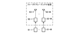
図8は、実施の形態5に係るフェーズドアレーアンテナ装置を示す構成図である。
図8において、送信器91-m(m=1,・・・,M)は、送信信号を移相器92-mに出力する。Mは、2以上の整数である。
移相器92-mは、実施の形態1~4のうちのいずれかの実施の形態に係る移相器1である。
移相器92-mは、送信器91-mから出力された送信信号を移相し、移相後の送信信号をアンテナ素子93-mに出力する。
アンテナ素子93-mは、移相器92-mによる移相後の送信信号に係る電波を空間に放射する。FIG. 8 is a configuration diagram showing a phased array antenna apparatus according to
In FIG. 8, transmitter 91-m (m=1, . . . , M) outputs a transmission signal to phase shifter 92-m. M is an integer of 2 or more.
Phase shifter 92-m is
The phase shifter 92-m phase-shifts the transmission signal output from the transmitter 91-m and outputs the phase-shifted transmission signal to the antenna element 93-m.
The antenna element 93-m radiates into space radio waves associated with the transmission signal after the phase shift by the phase shifter 92-m.
図8に示すフェーズドアレーアンテナ装置では、送信信号に係る電波を空間に放射している。しかし、これは一例に過ぎず、フェーズドアレーアンテナ装置は、電波を受信するものであってもよい。フェーズドアレーアンテナ装置のアンテナ素子93-mが、電波を受信する場合、アンテナ素子93-mが、電波の受信信号を移相器92-mに出力する。
移相器92-mは、アンテナ素子93-mから出力された受信信号を移相し、移相後の受信信号を図示せぬ受信器に出力する。The phased array antenna apparatus shown in FIG. 8 radiates radio waves associated with transmission signals into space. However, this is only an example, and the phased array antenna device may receive radio waves. When the antenna element 93-m of the phased array antenna apparatus receives radio waves, the antenna element 93-m outputs the received signal of the radio waves to the phase shifter 92-m.
The phase shifter 92-m phase-shifts the received signal output from the antenna element 93-m, and outputs the phase-shifted received signal to a receiver (not shown).
なお、本開示は、各実施の形態の自由な組み合わせ、あるいは各実施の形態の任意の構成要素の変形、もしくは各実施の形態において任意の構成要素の省略が可能である。 It should be noted that the present disclosure allows free combination of each embodiment, modification of arbitrary constituent elements of each embodiment, or omission of arbitrary constituent elements in each embodiment.
本開示は、移相器に適している。
本開示は、移相器を備えるフェーズドアレーアンテナ装置に適している。The present disclosure is suitable for phase shifters.
The present disclosure is suitable for phased array antenna apparatus with phase shifters.
1 移相器、11 第1の全域通過フィルタ、12 第2の全域通過フィルタ、13 第1の切替スイッチ、13a 接続端子、14 第2の切替スイッチ、14a 接続端子、15 第1の全域通過フィルタ、16 第2の全域通過フィルタ、17 第3の全域通過フィルタ、18 第4の全域通過フィルタ、20 第1の経路、20a 一端、20b 他端、21 第1のインダクタ、22 第1のキャパシタ、23 第2のキャパシタ、24 第2のインダクタ、25 第3のキャパシタ、30 第2の経路、30a 一端、30b 他端、31 第3のインダクタ、32 第4のキャパシタ、33 第5のキャパシタ、34 第4のインダクタ、35 第6のキャパシタ、41 第1のキャパシタ、42 第1のインダクタ、43 第2のインダクタ、44 第2のキャパシタ、45 第3のインダクタ、51 第3のキャパシタ、52 第4のインダクタ、53 第5のインダクタ、54 第4のキャパシタ、55 第6のインダクタ、61 位相基準回路、62 位相遅延回路、71,74 キャパシタ、72,73 インダクタ、81,84 キャパシタ、82,83 インダクタ、91-1~91-M 送信器、92-1~92-M 移相器、93-1~93-M アンテナ素子。
Claims (5)
複数の素子を含んでいる第2の全域通過フィルタと、
前記第1の全域通過フィルタ、又は、前記第2の全域通過フィルタのいずれか一方に信号を与える第1の切替スイッチと、
前記第1の全域通過フィルタを通過してきた信号、又は、前記第2の全域通過フィルタを通過してきた信号を選択する第2の切替スイッチとを備え、
前記第1の全域通過フィルタは、複数の素子として、第1のインダクタ、第2のインダクタ、第1のキャパシタ、第2のキャパシタ及び第3のキャパシタを含んでおり、
前記第2の全域通過フィルタは、複数の素子として、第3のインダクタ、第4のインダクタ、第4のキャパシタ、第5のキャパシタ及び第6のキャパシタを含んでおり、
前記第1のインダクタは、前記第1の切替スイッチと前記第2の切替スイッチとを結ぶ第1の経路に挿入されており、
前記第1のキャパシタの一端は、前記第1のインダクタの一端と接続されており、
前記第2のキャパシタの一端は、前記第1のインダクタの他端と接続されており、
前記第2のインダクタの一端は、前記第1のキャパシタ及び前記第2のキャパシタにおけるそれぞれの他端と接続されており、
前記第3のキャパシタの一端は、前記第2のインダクタの他端と接続され、前記第3のキャパシタの他端は、接地されており、
前記第3のインダクタは、前記第1の切替スイッチと前記第2の切替スイッチとを結ぶ第2の経路に挿入されており、
前記第4のキャパシタの一端は、前記第3のインダクタの一端と接続されており、
前記第5のキャパシタの一端は、前記第3のインダクタの他端と接続されており、
前記第4のインダクタの一端は、前記第4のキャパシタ及び前記第5のキャパシタにおけるそれぞれの他端と接続されており、
前記第6のキャパシタの一端は、前記第4のインダクタの他端と接続され、前記第6のキャパシタの他端は、接地されており、
前記第1の全域通過フィルタに含まれている複数の素子の素子値及び前記第2の全域通過フィルタに含まれている複数の素子の素子値が、インピーダンス整合を実現するインピーダンス、前記信号の周波数及び変数によって決定されていることを特徴とする移相器。 a first allpass filter including a plurality of elements;
a second allpass filter including a plurality of elements;
a first selector switch that provides a signal to either the first all-pass filter or the second all-pass filter;
a second changeover switch that selects a signal that has passed through the first all-pass filter or a signal that has passed through the second all-pass filter,
The first all-pass filter includes, as a plurality of elements, a first inductor, a second inductor, a first capacitor, a second capacitor, and a third capacitor,
the second all-pass filter includes, as a plurality of elements, a third inductor, a fourth inductor, a fourth capacitor, a fifth capacitor, and a sixth capacitor;
The first inductor is inserted in a first path connecting the first changeover switch and the second changeover switch,
one end of the first capacitor is connected to one end of the first inductor;
one end of the second capacitor is connected to the other end of the first inductor,
one end of the second inductor is connected to the other ends of the first capacitor and the second capacitor;
one end of the third capacitor is connected to the other end of the second inductor, the other end of the third capacitor is grounded;
the third inductor is inserted in a second path connecting the first changeover switch and the second changeover switch;
one end of the fourth capacitor is connected to one end of the third inductor;
one end of the fifth capacitor is connected to the other end of the third inductor,
one end of the fourth inductor is connected to the other ends of the fourth capacitor and the fifth capacitor,
one end of the sixth capacitor is connected to the other end of the fourth inductor, the other end of the sixth capacitor is grounded;
The element values of the plurality of elements included in the first all-pass filter and the element values of the plurality of elements included in the second all-pass filter are impedance matching and the frequency of the signal. and a variable.
前記第2の経路に挿入されている前記第2の全域通過フィルタが複数直列に接続されていることを特徴とする請求項1記載の移相器。 A plurality of the first all-pass filters inserted in the first path are connected in series,
2. A phase shifter according to claim 1, wherein a plurality of said second all-pass filters inserted in said second path are connected in series.
前記複数の第2の全域通過フィルタにおけるそれぞれの通過位相が互いに異なることを特徴とする請求項2記載の移相器。 Each pass phase in the plurality of first all-pass filters is different from each other,
3. The phase shifter according to claim 2 , wherein the pass phases of said plurality of second all-pass filters are different from each other.
2つのインダクタ及び2つのキャパシタを含んでいる第4の全域通過フィルタとを備え、
前記第3の全域通過フィルタが前記第1の全域通過フィルタと直列に接続されており、
前記第4の全域通過フィルタが前記第2の全域通過フィルタと直列に接続されていることを特徴とする請求項1記載の移相器。 a third allpass filter including two inductors and two capacitors;
a fourth allpass filter including two inductors and two capacitors;
the third all-pass filter is connected in series with the first all-pass filter;
2. The phase shifter of claim 1, wherein said fourth allpass filter is connected in series with said second allpass filter.
Applications Claiming Priority (1)
| Application Number | Priority Date | Filing Date | Title |
|---|---|---|---|
| PCT/JP2020/030932 WO2022038646A1 (en) | 2020-08-17 | 2020-08-17 | Phase shifter and phased array antenna device |
Publications (3)
| Publication Number | Publication Date |
|---|---|
| JPWO2022038646A1 JPWO2022038646A1 (en) | 2022-02-24 |
| JPWO2022038646A5 JPWO2022038646A5 (en) | 2022-09-15 |
| JP7150223B2 true JP7150223B2 (en) | 2022-10-07 |
Family
ID=80322869
Family Applications (1)
| Application Number | Title | Priority Date | Filing Date |
|---|---|---|---|
| JP2022543816A Active JP7150223B2 (en) | 2020-08-17 | 2020-08-17 | Phase shifter and phased array antenna device |
Country Status (4)
| Country | Link |
|---|---|
| US (1) | US20230106157A1 (en) |
| EP (1) | EP4175056A4 (en) |
| JP (1) | JP7150223B2 (en) |
| WO (1) | WO2022038646A1 (en) |
Citations (5)
| Publication number | Priority date | Publication date | Assignee | Title |
|---|---|---|---|---|
| JP2002076810A (en) | 2000-08-31 | 2002-03-15 | Mitsubishi Electric Corp | Phase shifter |
| JP2008211303A (en) | 2007-02-23 | 2008-09-11 | Mitsubishi Electric Corp | Phase shift circuit |
| JP2013098744A (en) | 2011-10-31 | 2013-05-20 | Sumitomo Electric Device Innovations Inc | Phase shifter and method of designing the same |
| JP2017123560A (en) | 2016-01-07 | 2017-07-13 | 学校法人上智学院 | Phase shifter |
| CN107332538A (en) | 2017-06-27 | 2017-11-07 | 中国科学院微电子研究所 | A kind of digital phase shifter |
Family Cites Families (1)
| Publication number | Priority date | Publication date | Assignee | Title |
|---|---|---|---|---|
| US7276993B2 (en) * | 2005-05-31 | 2007-10-02 | Agile Rf, Inc. | Analog phase shifter using cascaded voltage tunable capacitor |
-
2020
- 2020-08-17 WO PCT/JP2020/030932 patent/WO2022038646A1/en unknown
- 2020-08-17 EP EP20950212.9A patent/EP4175056A4/en active Pending
- 2020-08-17 JP JP2022543816A patent/JP7150223B2/en active Active
-
2022
- 2022-12-12 US US18/079,377 patent/US20230106157A1/en active Pending
Patent Citations (5)
| Publication number | Priority date | Publication date | Assignee | Title |
|---|---|---|---|---|
| JP2002076810A (en) | 2000-08-31 | 2002-03-15 | Mitsubishi Electric Corp | Phase shifter |
| JP2008211303A (en) | 2007-02-23 | 2008-09-11 | Mitsubishi Electric Corp | Phase shift circuit |
| JP2013098744A (en) | 2011-10-31 | 2013-05-20 | Sumitomo Electric Device Innovations Inc | Phase shifter and method of designing the same |
| JP2017123560A (en) | 2016-01-07 | 2017-07-13 | 学校法人上智学院 | Phase shifter |
| CN107332538A (en) | 2017-06-27 | 2017-11-07 | 中国科学院微电子研究所 | A kind of digital phase shifter |
Non-Patent Citations (1)
| Title |
|---|
| Xinyi Tang, Koen Mouthaan,Large Bandwidth Digital Phase Shifters With All-Pass, High-Pass, and Low-Pass Networks,IEEE TRANSACTIONS ON MICROWAVE THEORY AND TECHNIQUES,米国,IEEE,2013年,Vol.61, No.6,p.2325-2331,ISSN 0018-9480, 特に第2325-2326ページ,図1-2 |
Also Published As
| Publication number | Publication date |
|---|---|
| EP4175056A1 (en) | 2023-05-03 |
| US20230106157A1 (en) | 2023-04-06 |
| JPWO2022038646A1 (en) | 2022-02-24 |
| EP4175056A4 (en) | 2023-08-02 |
| WO2022038646A1 (en) | 2022-02-24 |
Similar Documents
| Publication | Publication Date | Title |
|---|---|---|
| US9712313B2 (en) | Systems for multi-peak-filter-based analog self-interference cancellation | |
| US7714681B2 (en) | Reconfigurable phase-shifter | |
| US7633358B2 (en) | Phase shifter circuit with proper broadband performance | |
| JP2009278618A (en) | Reflection-type phase shifter having reflection loads implemented using transmission lines and phased-array receiver/transmitter using the same | |
| AU2016361963B2 (en) | Beamforming engine | |
| US7417517B2 (en) | Method and apparatus for a communications filter | |
| US11784385B2 (en) | Wilkinson power combiner, communication unit and method therefor | |
| JP7150223B2 (en) | Phase shifter and phased array antenna device | |
| CN216251144U (en) | Miniaturized broadband digital phase shifter | |
| CN112271419B (en) | Ultra-wideband digital phase shifter with all-pass filter structure | |
| JP7099628B2 (en) | Phase shifter | |
| US20170085242A1 (en) | Phase shift circuit | |
| GB2543914A (en) | A microwave switched multiplexer and a mobile telecommunications device including such a multiplexer | |
| Xinyi | Broadband phase shifter design for phased array radar systems | |
| JP4864758B2 (en) | Orthogonal mixer and image rejection mixer | |
| US10505512B2 (en) | Tunable inductor circuit | |
| JP7034385B2 (en) | Delay circuit and line switching type phase shifter | |
| JP6566441B2 (en) | Phase shifter | |
| JPWO2022038646A5 (en) | ||
| CN216390945U (en) | Phase shift network | |
| TW201436469A (en) | Radio frequency bitstream generator and combiner providing image rejection | |
| CN111669148B (en) | Tunable bandpass filter, apparatus and method | |
| CN115694395A (en) | Broadband phase shift circuit | |
| KR20230102301A (en) | Dual-band 360 Degree Phase Shifter Using Series/Parallel Resonance Circuit for Phase Array Antenna System | |
| CN118017178A (en) | Broadband passive vector synthesis phase shifter |
Legal Events
| Date | Code | Title | Description |
|---|---|---|---|
| A521 | Request for written amendment filed |
Free format text: JAPANESE INTERMEDIATE CODE: A523 Effective date: 20220727 |
|
| A621 | Written request for application examination |
Free format text: JAPANESE INTERMEDIATE CODE: A621 Effective date: 20220727 |
|
| A871 | Explanation of circumstances concerning accelerated examination |
Free format text: JAPANESE INTERMEDIATE CODE: A871 Effective date: 20220727 |
|
| TRDD | Decision of grant or rejection written | ||
| A01 | Written decision to grant a patent or to grant a registration (utility model) |
Free format text: JAPANESE INTERMEDIATE CODE: A01 Effective date: 20220830 |
|
| A61 | First payment of annual fees (during grant procedure) |
Free format text: JAPANESE INTERMEDIATE CODE: A61 Effective date: 20220927 |
|
| R150 | Certificate of patent or registration of utility model |
Ref document number: 7150223 Country of ref document: JP Free format text: JAPANESE INTERMEDIATE CODE: R150 |