JP7147560B2 - Superluminescence diode and display device - Google Patents
Superluminescence diode and display device Download PDFInfo
- Publication number
- JP7147560B2 JP7147560B2 JP2018526005A JP2018526005A JP7147560B2 JP 7147560 B2 JP7147560 B2 JP 7147560B2 JP 2018526005 A JP2018526005 A JP 2018526005A JP 2018526005 A JP2018526005 A JP 2018526005A JP 7147560 B2 JP7147560 B2 JP 7147560B2
- Authority
- JP
- Japan
- Prior art keywords
- layer
- quantum well
- less
- guide
- conductivity type
- Prior art date
- Legal status (The legal status is an assumption and is not a legal conclusion. Google has not performed a legal analysis and makes no representation as to the accuracy of the status listed.)
- Active
Links
Images


Classifications
-
- H—ELECTRICITY
- H01—ELECTRIC ELEMENTS
- H01L—SEMICONDUCTOR DEVICES NOT COVERED BY CLASS H10
- H01L33/00—Semiconductor devices with at least one potential-jump barrier or surface barrier specially adapted for light emission; Processes or apparatus specially adapted for the manufacture or treatment thereof or of parts thereof; Details thereof
- H01L33/02—Semiconductor devices with at least one potential-jump barrier or surface barrier specially adapted for light emission; Processes or apparatus specially adapted for the manufacture or treatment thereof or of parts thereof; Details thereof characterised by the semiconductor bodies
- H01L33/26—Materials of the light emitting region
- H01L33/30—Materials of the light emitting region containing only elements of group III and group V of the periodic system
- H01L33/32—Materials of the light emitting region containing only elements of group III and group V of the periodic system containing nitrogen
-
- B—PERFORMING OPERATIONS; TRANSPORTING
- B82—NANOTECHNOLOGY
- B82Y—SPECIFIC USES OR APPLICATIONS OF NANOSTRUCTURES; MEASUREMENT OR ANALYSIS OF NANOSTRUCTURES; MANUFACTURE OR TREATMENT OF NANOSTRUCTURES
- B82Y20/00—Nanooptics, e.g. quantum optics or photonic crystals
-
- H—ELECTRICITY
- H01—ELECTRIC ELEMENTS
- H01L—SEMICONDUCTOR DEVICES NOT COVERED BY CLASS H10
- H01L33/00—Semiconductor devices with at least one potential-jump barrier or surface barrier specially adapted for light emission; Processes or apparatus specially adapted for the manufacture or treatment thereof or of parts thereof; Details thereof
- H01L33/02—Semiconductor devices with at least one potential-jump barrier or surface barrier specially adapted for light emission; Processes or apparatus specially adapted for the manufacture or treatment thereof or of parts thereof; Details thereof characterised by the semiconductor bodies
- H01L33/04—Semiconductor devices with at least one potential-jump barrier or surface barrier specially adapted for light emission; Processes or apparatus specially adapted for the manufacture or treatment thereof or of parts thereof; Details thereof characterised by the semiconductor bodies with a quantum effect structure or superlattice, e.g. tunnel junction
- H01L33/06—Semiconductor devices with at least one potential-jump barrier or surface barrier specially adapted for light emission; Processes or apparatus specially adapted for the manufacture or treatment thereof or of parts thereof; Details thereof characterised by the semiconductor bodies with a quantum effect structure or superlattice, e.g. tunnel junction within the light emitting region, e.g. quantum confinement structure or tunnel barrier
-
- H—ELECTRICITY
- H01—ELECTRIC ELEMENTS
- H01L—SEMICONDUCTOR DEVICES NOT COVERED BY CLASS H10
- H01L33/00—Semiconductor devices with at least one potential-jump barrier or surface barrier specially adapted for light emission; Processes or apparatus specially adapted for the manufacture or treatment thereof or of parts thereof; Details thereof
- H01L33/02—Semiconductor devices with at least one potential-jump barrier or surface barrier specially adapted for light emission; Processes or apparatus specially adapted for the manufacture or treatment thereof or of parts thereof; Details thereof characterised by the semiconductor bodies
- H01L33/08—Semiconductor devices with at least one potential-jump barrier or surface barrier specially adapted for light emission; Processes or apparatus specially adapted for the manufacture or treatment thereof or of parts thereof; Details thereof characterised by the semiconductor bodies with a plurality of light emitting regions, e.g. laterally discontinuous light emitting layer or photoluminescent region integrated within the semiconductor body
-
- H—ELECTRICITY
- H01—ELECTRIC ELEMENTS
- H01S—DEVICES USING THE PROCESS OF LIGHT AMPLIFICATION BY STIMULATED EMISSION OF RADIATION [LASER] TO AMPLIFY OR GENERATE LIGHT; DEVICES USING STIMULATED EMISSION OF ELECTROMAGNETIC RADIATION IN WAVE RANGES OTHER THAN OPTICAL
- H01S5/00—Semiconductor lasers
- H01S5/30—Structure or shape of the active region; Materials used for the active region
- H01S5/34—Structure or shape of the active region; Materials used for the active region comprising quantum well or superlattice structures, e.g. single quantum well [SQW] lasers, multiple quantum well [MQW] lasers or graded index separate confinement heterostructure [GRINSCH] lasers
- H01S5/3407—Structure or shape of the active region; Materials used for the active region comprising quantum well or superlattice structures, e.g. single quantum well [SQW] lasers, multiple quantum well [MQW] lasers or graded index separate confinement heterostructure [GRINSCH] lasers characterised by special barrier layers
-
- H—ELECTRICITY
- H01—ELECTRIC ELEMENTS
- H01S—DEVICES USING THE PROCESS OF LIGHT AMPLIFICATION BY STIMULATED EMISSION OF RADIATION [LASER] TO AMPLIFY OR GENERATE LIGHT; DEVICES USING STIMULATED EMISSION OF ELECTROMAGNETIC RADIATION IN WAVE RANGES OTHER THAN OPTICAL
- H01S5/00—Semiconductor lasers
- H01S5/30—Structure or shape of the active region; Materials used for the active region
- H01S5/34—Structure or shape of the active region; Materials used for the active region comprising quantum well or superlattice structures, e.g. single quantum well [SQW] lasers, multiple quantum well [MQW] lasers or graded index separate confinement heterostructure [GRINSCH] lasers
- H01S5/343—Structure or shape of the active region; Materials used for the active region comprising quantum well or superlattice structures, e.g. single quantum well [SQW] lasers, multiple quantum well [MQW] lasers or graded index separate confinement heterostructure [GRINSCH] lasers in AIIIBV compounds, e.g. AlGaAs-laser, InP-based laser
- H01S5/34333—Structure or shape of the active region; Materials used for the active region comprising quantum well or superlattice structures, e.g. single quantum well [SQW] lasers, multiple quantum well [MQW] lasers or graded index separate confinement heterostructure [GRINSCH] lasers in AIIIBV compounds, e.g. AlGaAs-laser, InP-based laser with a well layer based on Ga(In)N or Ga(In)P, e.g. blue laser
Description
本技術は、スーパールミネッセントダイオード(SLD)の技術に関する。 The present technology relates to superluminescent diode (SLD) technology.
スーパールミネッセントダイオード(SLD)は、発光ダイオードに比較的近い広い発光スペクトル幅を持ちながら、同時に半導体レーザの発光状態のような狭い放射角と強い強度で光を出射する特徴を持つ発光素子である。このSLDは、ファイバジャイロ等の干渉計分野に応用されている。近年では、その干渉性の低さから干渉ノイズの少ない画像投射用光源としてディスプレイへの応用も期待されている。 A superluminescent diode (SLD) is a light-emitting device that has a wide emission spectrum width that is relatively close to that of a light-emitting diode, and at the same time emits light with a narrow radiation angle and high intensity similar to that of a semiconductor laser. be. This SLD is applied in the field of interferometers such as fiber gyros. In recent years, due to its low coherence, it is expected to be applied to displays as a light source for image projection with little interference noise.
例えば、特許文献1には、直線状のリッジ導波路とこれに続く曲線状の導波路を備えるSLDが開示されている。リッジ導波路直下の活性層で発生した光は曲線状の導波路を進行し、SLDの端面に対して非垂直な方向に出射する。これにより、端面での反射光が導波路に戻ることが防止されている。
For example,
要するに、SLDは、通常のレーザダイオード(LD)のように、両端面に設けられたミラーで光を往復させて共振(レーザ発振)させる構造ではなく、光を導波路で一方通行させて光を増幅させる(誘導放出は行われる)構造を有する。最初の光の発生源はSLDの後端面(光出射端面とは反対側の端面)付近の活性層で発生した自然放出光である。SLDはこのスペクトル幅が広い光をそのまま導波路で増幅して強度を高め、出射する構造となっている。 In short, the SLD does not have a structure in which light is reciprocated by mirrors provided on both end surfaces to resonate (laser oscillation) as in a normal laser diode (LD), but is one-way light in a waveguide and emits light. It has a structure that amplifies (stimulated emission takes place). The first source of light is spontaneous emission light generated in the active layer near the rear facet of the SLD (the facet opposite to the light emitting facet). The SLD has a structure in which this light with a wide spectral width is amplified as it is in a waveguide to increase its intensity and is emitted.
上記のようなSLDにおいては、ディスプレイ等への応用のために出射光の出力向上が求められている。しかしながら、出射光の出力とスペクトル幅はトレードオフの関係にあり、出射光を高出力化し、かつ広いスペクトル幅を実現することは容易ではない。 In the SLD as described above, an improvement in the output of emitted light is required for application to displays and the like. However, there is a trade-off relationship between the output of the emitted light and the spectral width, and it is not easy to increase the output of the emitted light and achieve a wide spectral width.
以上のような事情に鑑み、本技術の目的は、高出力かつスペクトル幅の広い光を出射することが可能な光学素子、活性層構造及び表示装置を提供することにある。 In view of the circumstances as described above, an object of the present technology is to provide an optical element, an active layer structure, and a display device capable of emitting high-power light with a wide spectral width.
上記目的を達成するため、本技術の一形態に係る光学素子は、第1導電型層と、第2導電型層と、活性層とを具備する。
上記第1導電型層は、電流の注入領域が狭窄するように構成された電流狭窄構造を有する。
上記活性層は、上記第1導電型層と上記第2導電型層の間に設けられた活性層であって、1層の量子井戸層又は複数層の量子井戸層を有し、上記1層の量子井戸層の厚みは10nm以下であり、上記複数層の量子井戸層の厚みの合計は10nm以下である。To achieve the above object, an optical element according to one aspect of the present technology includes a first conductivity type layer, a second conductivity type layer, and an active layer.
The first conductivity type layer has a current confinement structure configured to constrict the current injection region.
The active layer is an active layer provided between the first conductivity type layer and the second conductivity type layer, and has a single quantum well layer or a plurality of quantum well layers, and the single layer The thickness of the quantum well layer is 10 nm or less, and the total thickness of the plurality of quantum well layers is 10 nm or less.
この構成によれば、量子井戸層の厚みを小さくすることにより、量子井戸への光閉じ込め効果が小さくなり、自然放出光の利用効率が小さくなる。このため、発光を開始するために必要なキャリア密度が大きくなり、単位体積当たりの自然放出光の発光量は大きくなる。また、自然放出光が増幅される利得領域においても、キャリア密度が大きいため、利得やスペクトル幅も大きくなる。これにより、光学素子の出射光を高出力かつスペクトル幅の広い光とすることが可能となる。 According to this configuration, by reducing the thickness of the quantum well layer, the effect of light confinement in the quantum well is reduced, and the utilization efficiency of spontaneous emission light is reduced. Therefore, the carrier density required to start light emission increases, and the amount of spontaneous emission light per unit volume increases. Moreover, since the carrier density is high in the gain region where the spontaneous emission light is amplified, the gain and the spectral width are also increased. As a result, the light emitted from the optical element can be light with a high output and a wide spectral width.
上記1層の量子井戸層又は上記複数層の量子井戸層は、AlInGaPからなるものであってもよい。 The single quantum well layer or the plurality of quantum well layers may be made of AlInGaP.
量子井戸層をAlInGaPからなるものとすることにより、赤色の光が光学素子から出射される。 By making the quantum well layer of AlInGaP, red light is emitted from the optical element.
上記活性層は、上記1層の量子井戸層を有し、
上記1層の量子井戸層はAlInGaNからなるものであってもよい。The active layer has the single quantum well layer,
The single quantum well layer may be made of AlInGaN.
量子井戸層をAlInGaNからなるものとすることにより、青紫色から緑色の光が光学素子から出射される。 By making the quantum well layer of AlInGaN, light of blue-violet to green color is emitted from the optical element.
上記第1導電型層は、第1クラッド層と、上記第1クラッド層と上記活性層の間に設けられた第1ガイド層とを有し、
上記第2導電型層は、第2クラッド層と、上記第2クラッド層と上記活性層の間に設けられた第2ガイド層とを有し、
上記第1ガイド層の厚さは10nm以上500nm以下であり、
上記第2ガイド層の厚さは10nm以上500nm以下であってもよい。The first conductivity type layer has a first cladding layer and a first guide layer provided between the first cladding layer and the active layer,
The second conductivity type layer has a second cladding layer and a second guide layer provided between the second cladding layer and the active layer,
The first guide layer has a thickness of 10 nm or more and 500 nm or less,
The second guide layer may have a thickness of 10 nm or more and 500 nm or less.
量子井戸への光閉じ込め率は、第1ガイド層及び第2ガイド層の厚さによって調整することができる。具体的にはこれらの層の厚さを10nm以上500nm以下とすることにより、量子井戸への光閉じ込め率を3%以下とすることができる。 The optical confinement rate in the quantum well can be adjusted by the thickness of the first guide layer and the second guide layer. Specifically, by setting the thickness of these layers to 10 nm or more and 500 nm or less, the optical confinement rate in the quantum well can be made 3% or less.
上記第1導電型層は、第1クラッド層と、上記第1クラッド層と上記活性層の間に設けられた第1ガイド層とを有し、
上記第2導電型層は、第2クラッド層と、上記第2クラッド層と上記活性層の間に設けられた第2ガイド層とを有し、
上記第1クラッド層と上記第1ガイド層の屈折率差は0.03以上0.50以下であり、
上記第2クラッド層と上記第2ガイド層の屈折率差は0.03以上0.50以下であってもよい。The first conductivity type layer has a first cladding layer and a first guide layer provided between the first cladding layer and the active layer,
The second conductivity type layer has a second cladding layer and a second guide layer provided between the second cladding layer and the active layer,
The refractive index difference between the first cladding layer and the first guide layer is 0.03 or more and 0.50 or less,
A refractive index difference between the second cladding layer and the second guide layer may be 0.03 or more and 0.50 or less.
量子井戸層がAlInGaPからなり、発光色が赤色の場合、第1クラッド層と第1ガイド層の屈折率差及び第2クラッド層と第2ガイド層の屈折率差を0.03以上0.50以下とすることにより、量子井戸への光閉じ込め率を3%以下とすることができる。 When the quantum well layer is made of AlInGaP and the emission color is red, the refractive index difference between the first clad layer and the first guide layer and the refractive index difference between the second clad layer and the second guide layer are 0.03 to 0.50. The optical confinement rate in the quantum well can be reduced to 3% or less by setting the following.
上記第1導電型層は、第1クラッド層と、上記第1クラッド層と上記活性層の間に設けられた第1ガイド層とを有し、
上記第2導電型層は、第2クラッド層と、上記第2クラッド層と上記活性層の間に設けられた第2ガイド層とを有し、
上記第1クラッド層と上記第1ガイド層の屈折率差は0.01以上0.10以下であり、
上記第2クラッド層と上記第2ガイド層の屈折率差は0.01以上0.10以下であってもよい。The first conductivity type layer has a first cladding layer and a first guide layer provided between the first cladding layer and the active layer,
The second conductivity type layer has a second cladding layer and a second guide layer provided between the second cladding layer and the active layer,
The refractive index difference between the first cladding layer and the first guide layer is 0.01 or more and 0.10 or less,
A refractive index difference between the second cladding layer and the second guide layer may be 0.01 or more and 0.10 or less.
量子井戸層がAlInGaNからなり、発光色が青紫色から緑色の場合、第1クラッド層と第1ガイド層の屈折率差及び第2クラッド層と第2ガイド層の屈折率差を0.01以上0.10以下とすることにより、量子井戸への光閉じ込め率を3%以下とすることができる。 When the quantum well layer is made of AlInGaN and the emission color is from bluish purple to green, the refractive index difference between the first clad layer and the first guide layer and the refractive index difference between the second clad layer and the second guide layer are 0.01 or more. By making it 0.10 or less, the optical confinement rate in the quantum well can be made 3% or less.
上記活性層は、量子井戸への光閉じ込め率が3%以下であってもよい。 The active layer may have an optical confinement rate in the quantum well of 3% or less.
量子井戸への光閉じ込め率を3%以下とすることにより、上記のように光学素子の出射光を高出力かつスペクトル幅の広い光とすることが可能となる。 By setting the light confinement ratio in the quantum well to 3% or less, it is possible to make the light emitted from the optical element high in output and light with a wide spectral width as described above.
上記目的を達成するため、本技術の一形態に係る光学素子は、第1導電型層と、第2導電型層と、活性層とを具備する。
上記第1導電型層は、電流の注入領域が狭窄するように構成された電流狭窄構造を有する。
上記活性層は、上記第1導電型層と上記第2導電型層の間に設けられた活性層であって、1層の量子井戸層又は複数層の量子井戸層を有し、量子井戸への光閉じ込め率が3%以下である。To achieve the above object, an optical element according to one aspect of the present technology includes a first conductivity type layer, a second conductivity type layer, and an active layer.
The first conductivity type layer has a current confinement structure configured to constrict the current injection region.
The active layer is an active layer provided between the first conductivity type layer and the second conductivity type layer, and has a single quantum well layer or a plurality of quantum well layers. has an optical confinement rate of 3% or less.
量子井戸への光閉じ込め率を3%以下とすることにより、上記のように光学素子の出射光を高出力かつスペクトル幅の広い光とすることが可能となる。 By setting the light confinement ratio in the quantum well to 3% or less, it is possible to make the light emitted from the optical element high in output and light with a wide spectral width as described above.
上記1層の量子井戸層又は上記複数層の量子井戸層は、AlInGaPからなるものであってもよい。 The single quantum well layer or the plurality of quantum well layers may be made of AlInGaP.
上記活性層は、上記1層の量子井戸層を有し、
上記1層の量子井戸層はAlInGaNからなるものであってもよい。The active layer has the single quantum well layer,
The single quantum well layer may be made of AlInGaN.
上記第1導電型層は、第1クラッド層と、上記第1クラッド層と上記活性層の間に設けられた第1ガイド層とを有し、
上記第2導電型層は、第2クラッド層と、上記第2クラッド層と上記活性層の間に設けられた第2ガイド層とを有し、
上記第1ガイド層の厚さは10nm以上500nm以下であり、
上記第2ガイド層の厚さは10nm以上500nm以下であってもよい。The first conductivity type layer has a first cladding layer and a first guide layer provided between the first cladding layer and the active layer,
The second conductivity type layer has a second cladding layer and a second guide layer provided between the second cladding layer and the active layer,
The first guide layer has a thickness of 10 nm or more and 500 nm or less,
The second guide layer may have a thickness of 10 nm or more and 500 nm or less.
上記第1ガイド層の厚さは50nm以上200nm以下であり、
上記第2ガイド層の厚さは50nm以上200nm以下であってもよい。The first guide layer has a thickness of 50 nm or more and 200 nm or less,
The second guide layer may have a thickness of 50 nm or more and 200 nm or less.
発光パターンの制御(出射光の広がり)やキャリアの閉じ込めを考慮すると、第1ガイド層及び第2ガイド層の厚さは50nm以上200nm以下がより好適である。 Considering the control of the emission pattern (spreading of emitted light) and the confinement of carriers, the thickness of the first guide layer and the second guide layer is more preferably 50 nm or more and 200 nm or less.
上記第1導電型層は、第1クラッド層と、上記第1クラッド層と上記活性層の間に設けられた第1ガイド層とを有し、
上記第2導電型層は、第2クラッド層と、上記第2クラッド層と上記活性層の間に設けられた第2ガイド層とを有し、
上記第1クラッド層と上記第1ガイド層の屈折率差は0.03以上0.50以下であり、
上記第2クラッド層と上記第2ガイド層の屈折率差は0.03以上0.50以下であってもよい。The first conductivity type layer has a first cladding layer and a first guide layer provided between the first cladding layer and the active layer,
The second conductivity type layer has a second cladding layer and a second guide layer provided between the second cladding layer and the active layer,
The refractive index difference between the first cladding layer and the first guide layer is 0.03 or more and 0.50 or less,
A refractive index difference between the second cladding layer and the second guide layer may be 0.03 or more and 0.50 or less.
上記第1クラッド層と上記第1ガイド層の屈折率差は0.06以上0.30以下であり、
上記第2クラッド層と上記第2ガイド層の屈折率差は0.06以上0.30以下であってもよい。The refractive index difference between the first cladding layer and the first guide layer is 0.06 or more and 0.30 or less,
A refractive index difference between the second cladding layer and the second guide layer may be 0.06 or more and 0.30 or less.
発光色が赤色の場合、発光パターンの制御(出射光の広がり)やキャリアの閉じ込めを考慮すると、第1クラッド層と第1ガイド層の屈折率差及び第2クラッド層と第2ガイド層の屈折率差は0.06以上0.30以下が好適である。 When the emission color is red, the difference in refractive index between the first cladding layer and the first guide layer and the refraction between the second cladding layer and the second guide layer are considered to control the emission pattern (spread of emitted light) and to confine carriers. The ratio difference is preferably 0.06 or more and 0.30 or less.
上記第1導電型層は、第1クラッド層と、上記第1クラッド層と上記活性層の間に設けられた第1ガイド層とを有し、
上記第2導電型層は、第2クラッド層と、上記第2クラッド層と上記活性層の間に設けられた第2ガイド層とを有し、
上記第1クラッド層と上記第1ガイド層の屈折率差は0.01以上0.10以下であり、
上記第2クラッド層と上記第2ガイド層の屈折率差は0.01以上0.10以下であってもよい。The first conductivity type layer has a first cladding layer and a first guide layer provided between the first cladding layer and the active layer,
The second conductivity type layer has a second cladding layer and a second guide layer provided between the second cladding layer and the active layer,
The refractive index difference between the first cladding layer and the first guide layer is 0.01 or more and 0.10 or less,
A refractive index difference between the second cladding layer and the second guide layer may be 0.01 or more and 0.10 or less.
上記第1クラッド層と上記第1ガイド層の屈折率差は0.02以上0.06以下であり、
上記第2クラッド層と上記第2ガイド層の屈折率差は0.02以上0.06以下であってもよい。The refractive index difference between the first cladding layer and the first guide layer is 0.02 or more and 0.06 or less,
A refractive index difference between the second cladding layer and the second guide layer may be 0.02 or more and 0.06 or less.
発光色が青紫色から緑色の場合発光パターンの制御(出射光の広がり)やキャリアの閉じ込めを考慮すると、第1クラッド層と第1ガイド層の屈折率差及び第2クラッド層と第2ガイド層の屈折率差は0.02以上0.06以下が好適である。 When the emission color is from bluish purple to green Considering the control of the emission pattern (spread of emitted light) and the confinement of carriers, the difference in refractive index between the first clad layer and the first guide layer and the second clad layer and the second guide layer is preferably 0.02 or more and 0.06 or less.
上記光学素子は、スーパールミネッセンスダイオードであってもよい。 The optical element may be a superluminescence diode.
上記光学素子は、光増幅器であってもよい。 The optical element may be an optical amplifier.
上記目的を達成するため、本技術の一形態に係る活性層構造は、電流の注入領域が狭窄するように構成された電流狭窄構造を有する第1導電型層と、第2導電型層と、上記第1導電型層と上記第2導電型層の間に設けられた活性層とを具備する光学素子の活性層構造である。
上記活性層は、1層の量子井戸層又は複数層の量子井戸層を有し、上記1層の量子井戸層の厚みは10nm以下であり、上記複数層の量子井戸層の厚みの合計は10nm以下である。In order to achieve the above object, an active layer structure according to an embodiment of the present technology includes a first conductivity type layer having a current confinement structure configured to constrict a current injection region, a second conductivity type layer, It is an active layer structure of an optical element comprising an active layer provided between the first conductivity type layer and the second conductivity type layer.
The active layer has one quantum well layer or multiple quantum well layers, the thickness of the single quantum well layer is 10 nm or less, and the total thickness of the multiple quantum well layers is 10 nm. It is below.
上記目的を達成するため、本技術の一形態に係る表示装置は、光学素子と、画像生成部とを具備する。
上記画像生成部は、上記光学素子から出射された光を2次元状にスキャン可能であり、画像データに基づき、投射される上記光による輝度を制御可能である。
上記光学素子は、第1導電型層と、第2導電型層と、活性層とを具備する。
上記第1導電型層は、電流の注入領域が狭窄するように構成された電流狭窄構造を有する。
上記活性層は、上記第1導電型層と上記第2導電型層の間に設けられた活性層であって、1層の量子井戸層又は複数層の量子井戸層を有し、上記1層の量子井戸層の厚みは10nm以下であり、上記複数層の量子井戸層の厚みの合計は10nm以下である。To achieve the above object, a display device according to one embodiment of the present technology includes an optical element and an image generator.
The image generator can two-dimensionally scan the light emitted from the optical element, and can control the brightness of the projected light based on image data.
The optical element includes a first conductivity type layer, a second conductivity type layer, and an active layer.
The first conductivity type layer has a current confinement structure configured to constrict the current injection region.
The active layer is an active layer provided between the first conductivity type layer and the second conductivity type layer, and has a single quantum well layer or a plurality of quantum well layers, and the single layer The thickness of the quantum well layer is 10 nm or less, and the total thickness of the plurality of quantum well layers is 10 nm or less.
以上、本技術によれば、高出力かつスペクトル幅の広い光を出射することが可能な光学素子、活性層構造及び表示装置を提供することができる。なお、ここに記載された効果は必ずしも限定されるものではなく、本開示中に記載されたいずれかの効果であってもよい。 As described above, according to the present technology, it is possible to provide an optical element, an active layer structure, and a display device capable of emitting high-power light with a wide spectral width. Note that the effects described here are not necessarily limited, and may be any of the effects described in the present disclosure.
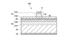
(光学素子の構造)
図1Aは、本技術の一実施形態に係る光学素子100を示す模式的な斜視図であり、図1Bはその平面図である。図2は、図1BにおけるC-C断面図である。この光学素子は、例えばp型またはn型の導電層にリッジ部10を有するリッジ型のスーパールミネッセントダイオード(SLD)である。(Structure of optical element)
FIG. 1A is a schematic perspective view showing an
光学素子100は、図2において上から、p型電極層(または図示しないp型電極層に接するコンタクト層)11、半導体層のうちp型である第1導電型層13、活性層20、半導体層のうちn型である第2導電型層14、n型半導体の基板15、n型電極層(または図示しないn型電極層に接するコンタクト層)12を備える。
The
第1導電型層13は、p型電極層11側から順に形成されたp型クラッド層131及びp型ガイド層132を有する。第2導電型層14は、基板15側から順に形成されたn型クラッド層141及びn型ガイド層142を有する。例えば、p型電極層11及びp型クラッド層131によりリッジ部10が構成される。基板15と第2導電型層14との間には、n型のバッファ層が設けられていてもよい。図1Bに示すように、光学素子100は光出射端面33と、光出射端面33に対して反対側の端面である後端面35を備える。
The first
図1Bに示すようにリッジ部10は、直線状部分10aと曲線状部分10bを有する。直線状部分10aは後端面35に対して垂直方向に沿って直線状に延伸されており、曲線状部分10bは直線状部分10aに連続して曲線状に延伸されている。なお、リッジ部10は、必ずしも直線状部分10aと曲線状部分10bを有するものでなくてもよく、後端面35から光出射端面33にかけて直線状に構成されていてもよい。
As shown in FIG. 1B, the
第1導電型層13は、図2に示すように電流狭窄構造32を有する。具体的には、リッジ部10の構造により、p型電極層11からの活性層20までの電流の注入領域が狭窄するように構成された電流狭窄構造32が形成される。これにより、活性層20におけるリッジ部10付近に、リッジ部10の長手方向に沿った光導波路が形成される。
The first
p型ガイド層132上やリッジ部10の周囲には、図示しない絶縁層が形成される。
An insulating layer (not shown) is formed on the p-
なお、p型クラッド層131の下端は、リッジ部10の下端と一致しているが、そうでなくてもよいし、当該リッジ部10の下端がp型ガイド層132の一部を含んでいてもよい。
Although the lower end of the p-
図1Bに示すように、光出射端面33には低反射ミラー膜18が設けられ、その反対側の後端面35には高反射ミラー膜19が設けられている。
As shown in FIG. 1B, a low-
p型電極層11とn型電極層12の間に電流を印加すると、後端面35近傍の活性層20で自然放出光が生じる。自然放出光は、光導波路を光出射端面33に向かって進行しながら誘導放出により増幅される。自然放出光のうち後端面35側に向かう光は、高反射ミラー膜19によって反射され、光出射端面33に向かって進行しながら増幅される。増幅された光は低反射ミラー膜18を介して光出射端面33から出射される。図1A及び図1Bに光学素子100の出射光Lを示す。
When a current is applied between the p-
リッジ部10が直線状部分10aと曲線状部分10bを有することにより、活性層20から出射される光は光出射端面33に対して垂直方向から傾斜した方向に出射される。これにより、低反射ミラー膜18でわずかに生じる反射光が活性層20に戻ることが防止されている。低反射ミラー膜18での反射光が活性層20に戻るとレーザ発振が生じるためである。
Since the
なお、上記のようにリッジ部10は直線状部分のみから構成されていてもよい。また、高反射ミラー膜19に変えて低反射ミラー膜を設けてもよい。この場合、光学素子100の出射光は光学素子100の両端から出射される。
It should be noted that the
光学素子100はSLDとして利用することができるが、他の光源で発生した光を増幅するための増幅器としても利用することができる。この場合には高反射ミラー膜19に変えて無反射膜が設けられる。他の光源で発生した光は当該無反射膜を介して光導波路に入射し、光導波路を進行しながら増幅される。
The
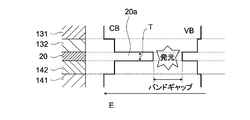
(活性層の構造)
光学素子100の活性層構造について説明する。図3は、各層のバンド構造を示す模式図である。横方向はエネルギー(図中、E)を示し、左側へ向かうほどエネルギーが高いことを示す。縦方向は光学素子100を構成する各層の積層方向を示す。エネルギーが低い側のバンドは価電子帯(VB:valence band)であり、エネルギーが高い側のバンドは伝導帯(CB:conduction band)である。(Structure of active layer)
The active layer structure of the
活性層20は、単層の量子井戸層20aを有する。量子井戸層20aは図3に示すように、周囲の層(p型ガイド層132及びn型ガイド層142)よりバンドギャップが小さい層である。p型電極層11とn型電極層12の間に電流が印加されると、伝導帯(CB)に存在する電子が量子井戸層20aのバンドギャップを介して価電子帯(VB)の正孔と再結合し、発光を生じる。この量子井戸層20aのバンドギャップは、発光再結合準位エネルギーギャップと呼ばれる。
The
(量子井戸層の厚みについて)
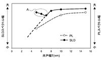
量子井戸層20aの厚みTは、量子井戸層20aが形成する量子井戸の幅であり、以下、単位に井戸幅Tとする。井戸幅Tは、10nm以下が好適である。(Regarding the thickness of the quantum well layer)
The thickness T of the
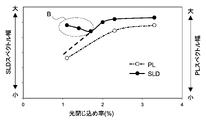
図4は、井戸幅TとSLDスペクトル幅(左軸)の関係及び井戸幅TとPLスペクトル幅(右軸)の関係を示すグラフである。SLDスペクトル幅は、光学素子100から出射される光(SLD)のスペクトル幅であり、PLスペクトル幅は、量子井戸層20aで生じる自然放出光(PL:Photoluminescence)のスペクトル幅である。
FIG. 4 is a graph showing the relationship between the well width T and the SLD spectrum width (left axis) and the relationship between the well width T and the PL spectrum width (right axis). The SLD spectral width is the spectral width of light (SLD) emitted from the
同図に示すように、井戸幅Tを小さくするとPLスペクトル幅は小さくなる。これは、井戸幅Tが小さくなると発光に寄与する量子井戸内の遷移準位が少なくなるためである。このため、従来では単層で薄い量子井戸層をSLDに用いる理由はなかった。 As shown in the figure, when the well width T is decreased, the PL spectrum width is decreased. This is because the smaller the well width T, the smaller the transition level in the quantum well that contributes to light emission. For this reason, conventionally, there was no reason to use a single-layer thin quantum well layer for an SLD.
例えば、従来のSLDの構造としては、複数の薄い量子井戸を有する活性層を備えた構造(以下、従来構造1)がある。この構造では、スペクトル幅の拡大のため、各量子井戸の波長を様々に変え、広いスペクトル幅を得る構造となっている。一方、複数の量子井戸を備えた構造では、注入キャリアが複数の量子井戸に分散され、キャリア分布が不均一となり易く、高利得が得にくい。 For example, as a structure of a conventional SLD, there is a structure provided with an active layer having a plurality of thin quantum wells (hereinafter referred to as conventional structure 1). In this structure, the wavelength of each quantum well is changed variously to obtain a wide spectrum width in order to widen the spectrum width. On the other hand, in a structure with a plurality of quantum wells, the injected carriers are dispersed among the plurality of quantum wells, the carrier distribution tends to become uneven, and it is difficult to obtain a high gain.
このため、単層で厚い量子井戸を有する活性層を備えたSLD(以下、従来構造2)が開発されている。この構造では、単層の量子井戸にキャリアが集中し、その中に含まれる多くのエネルギー準位で様々な波長の発光が生じる。しかしながらこの構造でも出力は不十分であり、特にディスプレイ用途には不適である。 For this reason, an SLD having an active layer having a single layer and a thick quantum well (hereinafter referred to as conventional structure 2) has been developed. In this structure, carriers are concentrated in a single-layer quantum well, and the many energy levels contained therein produce emission of different wavelengths. However, even this structure has a poor output and is particularly unsuitable for display applications.
これに対し、本実施形態に係る活性層20は上記のように、単層で薄い量子井戸層20aを有する。井戸幅Tが小さくなると、PLスペクトル幅が小さくなることから、SLDスペクトル幅も小さくなる(図中、破線)と予測された。
On the other hand, the
しかしながら、実際には、井戸幅Tを小さくすると図中囲みAに示すようにSLDスペクトル幅が向上することが判明した。図5は、上記従来構造のSLDと本実施形態に係るSLDの特性を表す表である。 However, in practice, it has been found that the SLD spectrum width is improved as indicated by box A in the figure when the well width T is reduced. FIG. 5 is a table showing the characteristics of the SLD having the conventional structure and the SLD according to the present embodiment.
同図の「本実施形態」に示すように、井戸幅Tを小さくすると、量子井戸での光閉じ込め効果が小さくなり、自然放出光(SLD発光の源となる光)の光導波路への結合割合が小さくなるため、自然放出光の利用効率が小さくなる。 As shown in "this embodiment" in the figure, when the well width T is reduced, the light confinement effect in the quantum well is reduced, and the coupling ratio of the spontaneous emission light (light that is the source of SLD light emission) to the optical waveguide is reduced. becomes smaller, the utilization efficiency of the spontaneous emission light becomes smaller.
このため、SLD発光を開始するためには従来構造に対して数倍高いキャリア密度が必要となる。この結果、SLD発光の開始時にはキャリア密度が大きいため、単位体積当たりの自然放出光の発光量は大きくなる。また、自然放出光が増幅される利得領域(自然放出光が増幅される領域)においても、キャリア密度が大きいため、利得やスペクトル幅も大きくなる。 Therefore, in order to initiate SLD light emission, a carrier density several times higher than that of the conventional structure is required. As a result, since the carrier density is high at the start of SLD light emission, the amount of spontaneous emission light per unit volume increases. Also, in the gain region where the spontaneous emission light is amplified (the region where the spontaneous emission light is amplified), the gain and spectrum width are also increased because the carrier density is high.
図6はキャリア密度によるスペクトル幅と利得の関係を示すグラフである。同図に示すように、SLD発光開始時のキャリア密度が大きいと、スペクトル幅と利得の両者が向上する。 FIG. 6 is a graph showing the relationship between spectrum width and gain depending on carrier density. As shown in the figure, when the carrier density at the start of SLD emission is high, both the spectral width and the gain are improved.
さらに、井戸幅Tが小さく、キャリア密度が大きいために量子井戸の量子効果が大きくなり、注入キャリアの利用効率が促進され、出力改善や温度特性の改善も達成される。また、活性層20の体積減少により活性層ロスも低減する。
Furthermore, since the well width T is small and the carrier density is high, the quantum effect of the quantum well is increased, the utilization efficiency of the injected carriers is promoted, and the output and temperature characteristics are improved. Also, the reduction in the volume of the
結果として、井戸幅Tが小さいと困難とされていた広いスペクトル幅を実現し、高出力及び高効率も同時に達成することが可能となる。 As a result, it is possible to achieve a wide spectrum width, which has been considered difficult if the well width T is small, and to achieve high output and high efficiency at the same time.
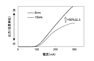
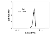
図7は、光学素子100に供給される電流と光学素子100の出射光の出力の関係を示すグラフであり、井戸幅Tが6nmの場合と15nmの場合についての計算結果である。同図に示すように、井戸幅Tが6nmの場合、15nmの場合に比べて出射光の出力が30%以上向上している。
FIG. 7 is a graph showing the relationship between the current supplied to the
また、グラフの最大電流付近では15nmの場合に出力飽和がみられるのに対し、6nmの場合には出力飽和がみられない。このため、より高い電流では両者の差はさらに開くと予想される。また、この計算では、自己発熱効果も考慮されており、高電流域での動作での出力が特に改善されている結果から、高温での動作も6nmの場合が優位である。 Further, in the vicinity of the maximum current in the graph, output saturation is observed in the case of 15 nm, but output saturation is not observed in the case of 6 nm. Therefore, the gap between the two is expected to widen even further at higher currents. Also, in this calculation, the self-heating effect is also taken into consideration, and from the result that the output is particularly improved in the operation in the high current range, the case of 6 nm is superior in the operation at high temperature.
また、図8は、光学素子100の出射光の波長と強度の関係を示すグラフであり、井戸幅Tが6nmの場合と15nmの場合についての計算結果である。同図に示すように、井戸幅Tが6nmの場合、15nmの場合に対してスペクトル幅やスペクトル形状が同等である。
FIG. 8 is a graph showing the relationship between the wavelength and intensity of light emitted from the
この他にも井戸幅Tが6nmの場合、15nmの場合と比べて温度特性が改善されており、ビーム形状も15nmの場合と同等となる。このように、井戸幅Tを10nm以下とすることにより、SLD光の立ち上がり電流低減、SLD光のスペクトル幅維持、発光効率の改善及び温度特性改善等を達成することが可能である。 In addition, when the well width T is 6 nm, the temperature characteristics are improved as compared to when the well width is 15 nm, and the beam shape is also the same as when the well width is 15 nm. Thus, by setting the well width T to 10 nm or less, it is possible to reduce the rising current of the SLD light, maintain the spectrum width of the SLD light, improve the light emission efficiency, improve the temperature characteristics, and the like.
なお、井戸幅Tについては10nm以下が好適であるが、特性改善のためにはさらなる薄膜化によるキャリアの有効活用促進が有効であり、光学素子100製造時のエピタキシャル成長のプロセス上、結晶性を損なわないレベルで極薄化されることが望ましい。特に井戸幅Tが7nm以下の場合に効果が大きく、好適である。 Although the well width T is preferably 10 nm or less, in order to improve the characteristics, it is effective to promote effective use of carriers by further thinning the film. It is desirable to be ultra-thin at a level that does not In particular, the effect is great when the well width T is 7 nm or less, which is preferable.
また、井戸幅Tが小さくなり、即ち活性層20の体積が低下した分だけ、非励起領域の活性層光吸収の光損失も低減し、活性層周辺の発熱源が小さくなることがわかっており、さらなる発光効率、またはエネルギー効率の改善の促進、素子内温度の低下、ひいては信頼性の改善にも効果がある。
In addition, it is known that as the well width T becomes smaller, that is, the volume of the
(量子井戸への光閉じ込め率について)
量子井戸層20aが形成する量子井戸への光閉じ込め率は3%以下が好適である。量子井戸への光閉じ込め率は、量子井戸に閉じ込められる光密度の割合を意味し、従来では量子井戸への光閉じ込め率は4%以上が一般的である。(Regarding the optical confinement ratio in the quantum well)
The light confinement rate in the quantum well formed by the
上記のように井戸幅Tを小さくすると量子井戸への光閉じ込め率は小さくなり、量子井戸層20aで生じる自然放出光のスペクトル幅は小さくなる。図9は、量子井戸への光閉じ込め率とSLDスペクトル幅(左軸)の関係及び同閉じ込め率とPLスペクトル幅(右軸)の関係を示すグラフである。
When the well width T is reduced as described above, the light confinement rate in the quantum well is reduced, and the spectrum width of spontaneous emission light generated in the
同図に示すように、量子井戸への光閉じ込め率が小さくなるとPLスペクトル幅が小さくなることから、SLDスペクトル幅も小さくなる(図中、破線)と予測された。しかしながら、実際には、量子井戸への光閉じ込め率を小さくすると、図中囲みBに示すようにSLDスペクトル幅が向上することが判明した。 As shown in the figure, it was predicted that the SLD spectral width would also decrease (broken line in the figure) because the PL spectral width would decrease as the optical confinement ratio in the quantum well decreased. However, in practice, it was found that reducing the optical confinement ratio in the quantum well improves the SLD spectral width as indicated by box B in the figure.
これは、図5に示すように、量子井戸への光閉じ込め率が小さく、自然放出光の利用効率が小さくなると、SLD発光の開始時に高いキャリア密度が必要となり、上述のように量子井戸の量子効果が大きくなること及び活性層ロスが低減することによる。このように量子井戸への光閉じ込め率を3%以下とすることにより、広いスペクトル幅を実現し、高出力及び高効率も同時に達成することが可能である。 This is because, as shown in FIG. 5, when the light confinement ratio in the quantum well is small and the utilization efficiency of spontaneously emitted light is low, a high carrier density is required at the start of SLD light emission, and as described above, the quantum well of the quantum well This is due to greater effectiveness and reduced active layer loss. By setting the optical confinement rate in the quantum well to 3% or less in this way, it is possible to achieve a wide spectrum width, high output power, and high efficiency at the same time.
(量子井戸層の条件について)
上記のように、量子井戸層20aの厚み(井戸幅T)は10nm以下が好適であり、量子井戸層20aが形成する量子井戸への光閉じ込め率は3%以下が好適である。本実施形態に係る光学素子100は、量子井戸層20aの厚みが10nm以下という条件と、量子井戸への光閉じ込め率が3%以下という条件のうち、少なくともいずれか一方を満たすものであればよい。(Regarding the condition of the quantum well layer)
As described above, the thickness (well width T) of the
(量子井戸層の材料について)
量子井戸層20aの材料は特に限定されないが、光学素子100の発光色は量子井戸層20aの材料によって異なる。例えば、量子井戸層20aがAlInGaPからなる場合、発光波長550~900nm(実用域630~680nm)の赤色光が生成される。また、量子井戸層20aがAlInGaNからなる場合、発光波長400~1000nm(実用域400~550nm)の青紫色から緑色の光が生成される。(Regarding the material of the quantum well layer)
Although the material of the
この他にも量子井戸層20aの材料としてAlGaN(発光波長紫外域~400nm)、AlGaAs(発光波長750~850nm、赤外域)、InGaAs(発光波長800~980nm、赤外域)、InGaAsP(発光波長1.2~1.6μm、赤外域)等が挙げられる。
In addition, materials for the
(ガイド層及びクラッド層ついて)
p型ガイド層132及びn型ガイド層142の厚みによって、量子井戸への光閉じ込め率を3%以下に調整することができる。p型ガイド層132及びn型ガイド層142の厚みはそれぞれ10nm以上500nm以下が好適であり、50nm以上200nm以下がより好適である。(Regarding guide layer and clad layer)
Depending on the thickness of the p-
上記10nm以上500nm以下はSLDのデバイス設計で採り得る数値範囲であり、50nm以上200nmは、光の閉じ込めだけでなく、発光パターンの制御(出射光の広がり)やキャリアの閉じ込めも考慮した数値範囲である。 The range of 10 nm to 500 nm is a numerical range that can be adopted in SLD device design. be.
また、p型クラッド層131とp型ガイド層132の屈折率差(以下、p型屈折率差)及びn型クラッド層141とn型ガイド層142の屈折率差(以下、n型屈折率差)によって量子井戸への光閉じ込め率を3%以下に調整することもできる。
Further, the refractive index difference between the p-
具体的には、量子井戸層20aがAlInGaPからなり、発光色が赤色の場合、p型屈折率差及びn型屈折率差はそれぞれ0.03以上0.50以下が好適であり、0.06以上0.30以下がより好適である。
Specifically, when the
上記0.03以上0.50以下はSLDのデバイス設計で採り得る数値範囲であり、0.06以上0.30以下は、光の閉じ込めだけでなく、発光パターンの制御(出射光の広がり)やキャリアの閉じ込めも考慮した数値範囲である。 The above range of 0.03 to 0.50 is a numerical range that can be taken in SLD device design, and the range of 0.06 to 0.30 is not only for light confinement, but also for control of light emission pattern (spread of emitted light) and This numerical range also takes into consideration carrier confinement.
また、量子井戸層20aがAlInGaNからなり、発光色が青紫色から緑色の場合、p型屈折率差及びn型屈折率差はそれぞれ0.01以上0.10以下が好適であり、0.02以上0.06以下がより好適である。
Further, when the
上記0.01以上0.10以下はSLDのデバイス設計で採り得る数値範囲であり、0.02以上0.06以下は、光の閉じ込めだけでなく、発光パターンの制御(出射光の広がり)やキャリアの閉じ込めも考慮した数値範囲である。 The above range of 0.01 to 0.10 is a numerical range that can be adopted in SLD device design. This numerical range also takes into consideration carrier confinement.
p型クラッド層131、p型ガイド層132、n型クラッド層141及びn型ガイド層142の材料は特に限定されない。例えば、p型クラッド層131はMgがドープされたAl0.5In0.5P、p型ガイド層132はGaxIn1-xP、n型クラッド層141はGaxIn1-xP、n型ガイド層142はSiがドープされたAl0.5In0.5Pからなるものとすることができる。Materials for the p-type clad
(従来構造との比較による光学素子の効果について)
SLDの出力向上のためには、電流を多く注入する、導波路長を長くする、あるいはリッジ導波路の幅を大きくする等が考えられる。(About the effect of the optical element in comparison with the conventional structure)
In order to improve the output of the SLD, it is conceivable to inject more current, lengthen the waveguide length, or increase the width of the ridge waveguide.
しかしながら、電流を多く注入する場合、その上限値は出力の熱飽和によって制限されるため、高出力化のためには、実装あるいはパッケージへの放熱負担が大きくなる。これは高コスト化の原因となる他、わずかな端面反射でレーザ発振が生じやすくなるため、熱飽和による制限よりも大幅に低い電流で使用する必要がある。 However, when a large amount of current is injected, the upper limit is limited by the thermal saturation of the output, so the heat dissipation burden on the mounting or package becomes large in order to increase the output. In addition to increasing costs, laser oscillation is likely to occur due to slight end face reflection, so it is necessary to use a current much lower than the limit due to thermal saturation.
また、導波路長を長くする場合、光が出射されるまでの間により長い経路で増幅されるため、光強度が大きくなる。一方で誘導放出による光の増幅をより多く受けることによって利得スペクトラム(波長依存性)の影響を強く受け、発光スペクトル幅が狭くなる。このため、低コヒーレンス性が低下する。即ち、出力とコヒーレンスはトレードオフの関係を有する。さらに、導波路長を長い場合、SLDのサイズが大きくなり、パッケージの小型化に不向きとなる上、全体の導波ロスの影響が増え、光変化効率も低下する。 Further, when the waveguide length is increased, the light is amplified along a longer path until it is emitted, so the light intensity increases. On the other hand, as the light is amplified more by stimulated emission, the gain spectrum (wavelength dependence) is strongly affected, and the emission spectrum width is narrowed. Therefore, the low coherence property is deteriorated. That is, the output and coherence have a trade-off relationship. Furthermore, when the waveguide length is long, the size of the SLD becomes large, which is not suitable for miniaturization of the package, and the influence of the overall waveguide loss increases, and the light conversion efficiency also decreases.
また、リッジ導波路の幅を大きくする場合、電流密度の集中を緩和して発光する面積を増やすことにより、出力を高めることができる。しかしながら、出射されるビームの幅が広くなり、特別に光学系が必要となる等、光源として利用しにくくなる。さらに、リッジ導波路の幅を大きくすることで導波し得るモードが多くなるため、出力の不安定性の原因となる。 Further, when the width of the ridge waveguide is increased, the output can be increased by alleviating the current density concentration and increasing the light emitting area. However, the width of the emitted beam is widened and a special optical system is required, making it difficult to use as a light source. Furthermore, increasing the width of the ridge waveguide increases the number of modes that can be guided, which causes output instability.
この他にも、増幅を受ける前の自然放出光の段階でスペクトル幅を大きくする方法もあるが、そのためには、注入電極を分割して設置するか、活性層の材料や構造を部分毎に変更する必要がある。前者の場合には別々のドライバで分割電極を駆動する必要があり、高コストである。後者の場合には結晶の再成長が必要になる等、製造が困難であり、やはり高コストとなる。 In addition to this, there is a method of increasing the spectral width at the spontaneous emission stage before being amplified. need to change. In the former case, it is necessary to drive the segmented electrodes with separate drivers, resulting in high cost. In the latter case, regrowth of crystals is required, and production is difficult, resulting in high cost.
また、上記いずれの方法でも消費される電流が増加するため、光源としての効率は低下する。 In addition, in any of the above methods, the current consumed increases, so the efficiency as a light source decreases.
これに対し、本実施形態に係る光学素子100では、量子井戸層20aの厚みを10nm以下とし、または量子井戸への光閉じ込め率を3%以下とすることにより、高出力かつスペクトル幅の広い光を出射することが可能となっている。
On the other hand, in the
上記のように、従来構造では、スペクトル幅拡大と出力改善の間にトレードオフの関係があり、両特性の妥協点を考える素子設計が用いられていたが、本技術では、その制限を受けずに設計することが可能であり、より高い性能を両立できる。 As described above, in the conventional structure, there is a trade-off relationship between spectral width expansion and output improvement, and an element design that considers a compromise between the two characteristics was used. Therefore, it is possible to design for a higher performance at the same time.
また、後端面近傍での自然放出光の導波路結合が素子特性に直接影響する独特の動作原理を利用したSLDに好適な構造であり、特別な活性層製成膜方法を必要とせず、既存の成膜方法を用いて作製することができる。 In addition, the structure is suitable for SLDs that utilize a unique operating principle in which waveguide coupling of spontaneously emitted light near the rear facet directly affects device characteristics. can be produced using the film formation method of
さらに、量子井戸素の薄膜化による量子効果の増大によって光利得が改善されることでSLD出力を大幅に高め、かつ高温での特性劣化も抑制できる。また、追加される工程は、エピタキシャル成長での一部工程の変更のみであり、製造プロセス全体への影響は僅少である。 Further, the quantum effect is enhanced by thinning the quantum well element, thereby improving the optical gain, thereby greatly increasing the SLD output and suppressing the characteristic deterioration at high temperature. Moreover, the added process is only a partial change in the epitaxial growth process, and the effect on the entire manufacturing process is minimal.
活性層の組成及び膜厚に関しては、TEM(Transmission Electron Microscope)解析後でのEDX(Energy dispersive X-ray spectrometry)解析又はWDX(Wavelength Dispersive X-ray spectroscopy)解析で十分検出可能である。また、膜厚のみならず、光導波計算を組み合わせて光閉じ込め率算出も可能である。 The composition and thickness of the active layer can be sufficiently detected by EDX (Energy dispersive X-ray spectrometry) analysis or WDX (Wavelength Dispersive X-ray spectroscopy) analysis after TEM (Transmission Electron Microscope) analysis. In addition to the film thickness, it is also possible to calculate the optical confinement ratio by combining optical waveguide calculation.
さらに、用途に合わせて出力を共振器長により調整し、必要となるスペクトル幅と出力に調整することができる。また、薄い量子井戸層を用いることで、スペクトラムが単峰化しやすく、OCT(Optical Coherence Tomography)等の干渉を利用する用途でも、外乱の少ない測定結果を得る事ができる。 Furthermore, the output can be adjusted by adjusting the cavity length according to the application, and the spectral width and output can be adjusted as required. In addition, by using a thin quantum well layer, the spectrum tends to be unimodal, and measurement results with little disturbance can be obtained even in applications using interference such as OCT (Optical Coherence Tomography).
また、増幅器として利用する場合であっても、同様の効果が期待でき、同等の構造とすることによって増幅波長域の広帯域化、効率アップ等の機能向上を図ることができる。 In addition, even if it is used as an amplifier, the same effect can be expected, and by using the same structure, it is possible to widen the amplification wavelength band and improve the function such as efficiency improvement.
(量子井戸層の層数について)
上記実施形態においては活性層20は単層の量子井戸層20aを有するものとしたが、複数層の量子井戸層20aを有するものであってもよい。図10は、複数層の量子井戸層20aを有する活性層20におけるバンド構造を示す模式図である。(Regarding the number of quantum well layers)
Although the
同図に示すように、活性層20は複数層の量子井戸層20aを有し、各量子井戸層20aの間には障壁層20bが設けられている。なお、活性層20が有する量子井戸層20aの数は3層に限られず、2層又は4層以上であってもよいが、ここでは3層の量子井戸層20aを例にとって説明する。
As shown in the figure, the
それぞれの量子井戸層20aの厚みを厚みT1、厚みT2及び厚みT3とすると、量子井戸層20aの厚みの合計、即ち厚みT1、厚みT2及び厚みT3の合計は10nm以下が好適である。量子井戸層20aの数が2層又は4層以上の場合も同様に、量子井戸層20aの厚みの合計は10nm以下が好適である。
Assuming that the thicknesses of the quantum well layers 20a are T1, T2, and T3, the total thickness of the quantum well layers 20a, that is, the sum of the thicknesses T1, T2, and T3, is preferably 10 nm or less. Similarly, when the number of
これにより、活性層20が単層の量子井戸層20aを有する場合と同様の原理によって光学素子100は高出力かつスペクトル幅の広い光を出射することが可能となる。それぞれの量子井戸層20aの厚みは同一であってもよく、互いに異なってもよい。また、それぞれの量子井戸層20aのバンドギャップは同一であってもよく、互いに異なってもよい。
As a result, the
また、量子井戸層20aが形成する量子井戸への光閉じ込め率は3%以下が好適である。量子井戸への光閉じ込め率を3%以下とすることにより、広いスペクトル幅を実現し、高出力及び高効率も同時に達成することが可能である。
Also, the light confinement rate in the quantum well formed by the
活性層20が複数層の量子井戸層20aを有する場合であっても、量子井戸層20aの厚みの合計が10nm以下という条件と、量子井戸への光閉じ込め率が3%以下という条件のうち、少なくともいずれか一方を満たすものであればよい。
Even if the
図11は、複数層の量子井戸層20aを備える活性層20の具体的構成を示す模式図である。なお、同図では活性層20、p型ガイド層132及びn型ガイド層142以外の構成については図示を省略する。同図に示すように、活性層20は、量子井戸層20aと障壁層20bが交互に積層されて構成されている。
FIG. 11 is a schematic diagram showing a specific configuration of the
量子井戸層20aは、上述のようにAlInGaAlP(赤色)又はAlInGaN(青紫色から緑色)等の材料からなる。また、量子井戸層20aの間で材料が異なってもよい。障壁層20bは、例えばAlGaSs等からなるものとすることができる。
The
なお、活性層20以外の構成は活性層20が単層の量子井戸層20aを有する構造と同一とすることができる。即ち、p型ガイド層132及びn型ガイド層142の厚みやp型クラッド層131とp型ガイド層132の屈折率差及びn型ガイド層142とn型クラッド層141の屈折率差を上記範囲とすることにより、量子井戸への光閉じ込め率を3%以下とすることができる。
The structure other than the
(表示装置)
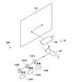
図12は、上記実施形態に係る光学素子であるSLDを光源として用いる表示装置の構成を模式的に示す。この表示装置200は、ラスタスキャン方式のプロジェクタである。(Display device)
FIG. 12 schematically shows the configuration of a display device using an SLD, which is an optical element according to the above embodiment, as a light source. The
表示装置200は、画像生成部70を備える。画像生成部70は、光源としての光学素子から出射された光を2次元状にスキャン可能、例えばラスタスキャン可能であり、画像データに基づき、スクリーンや壁面等の照射面105に投射される光による輝度を制御可能に構成される。
The
画像生成部70は、例えば水平スキャナ103及び垂直スキャナ104を主に含む。赤色発光の光学素子100R、緑色発光の光学素子100G及び青色発光の光学素子100Bからのビームのそれぞれは、ダイクロイックプリズム102R,102G,102Bによって1本のビームに纏められる。このビームが、水平スキャナ103及び垂直スキャナ104によってスキャンされ、照射面105に投影されることで画像が表示される。
The
なお、RGBの各色発光の光源のうち、少なくとも1つが本実施形態に係る光学素子100の構成を有するSLDであればよく、他の素子は通常のLDであってもよい。
It should be noted that at least one of the RGB color light sources may be an SLD having the configuration of the
水平スキャナ103及び垂直スキャナ104は、例えば、ポリゴンミラーとガルバノスキャナとの組合せにより構成される。この場合、輝度の制御手段としては、例えば光学素子へ注入する電流を制御する回路が用いられる。
The
あるいは、水平スキャナ及び垂直スキャナとして、例えば、MEMS(Micro Electro Mechanical System)技術を用いて製造されるDMD(Digital Micro-mirror Device)等の、2次元光変調素子が用いられてもよい。 Alternatively, a two-dimensional light modulation element such as a DMD (Digital Micro-mirror Device) manufactured using MEMS (Micro Electro Mechanical System) technology may be used as the horizontal scanner and the vertical scanner.
あるいは、画像生成部70は、GLV(Grating Light Valve)素子等の1次元光変調素子と、上述の1次元スキャンミラーとの組み合わせにより構成されていてもよい。
Alternatively, the
あるいは、画像生成部70は、音響光学効果スキャナや電気光学効果スキャナといった屈折率変調型スキャナにより構成されていてもよい。
Alternatively, the
(他の実施形態)
本技術は、以上説明した実施形態に限定されず、他の種々の実施形態を実現することができる。(Other embodiments)
The present technology is not limited to the embodiments described above, and various other embodiments can be implemented.
電流の注入領域が狭窄するように構成された電流狭窄構造32は、リッジ部10を構成する構造に限られない。例えば電流狭窄構造は、埋め込み型又は埋め込みリッジ型の構造であってもよい。
The
上記実施形態では、基板15としてn型基板が用いられたが、p型基板が用いられ、電流狭窄構造を構成する半導体層がn型であってもよい。この場合、「第1導電型」がn型、「第2導電型」がp型となる。
In the above embodiment, an n-type substrate is used as the
上記実施形態に係る光学素子は、活性層20を中心として基板15の反対側に電流狭窄構造32が配置される構成を有していた。しかし、活性層20を中心として基板(n型でもp型でもよい)と同じ側に電流狭窄構造が配置されていてもよい。ただし、上記実施形態の光学素子は、そのように基板と同じ側に電流狭窄構造が配置される構成を有する光学素子に比べ、構造上、放熱性が高いとうメリットがある。
The optical element according to the above embodiment had a configuration in which the
以上説明した他の実施形態の特徴部分のうち、少なくとも2つの特徴部分を組み合わせることも可能である。 It is also possible to combine at least two characteristic portions among the characteristic portions of the other embodiments described above.
なお、本技術は以下のような構成もとることができる。
(1)
電流の注入領域が狭窄するように構成された電流狭窄構造を有する第1導電型層と、
第2導電型層と、
上記第1導電型層と上記第2導電型層の間に設けられた活性層であって、1層の量子井戸層又は複数層の量子井戸層を有し、上記1層の量子井戸層の厚みは10nm以下であり、上記複数層の量子井戸層の厚みの合計は10nm以下である活性層と
を具備する光学素子。Note that the present technology can also have the following configuration.
(1)
a first conductivity type layer having a current confinement structure configured to constrict a current injection region;
a second conductivity type layer;
an active layer provided between the first-conductivity-type layer and the second-conductivity-type layer, the active layer having one quantum well layer or a plurality of quantum well layers; An optical element comprising: an active layer having a thickness of 10 nm or less, and having a total thickness of the plurality of quantum well layers of 10 nm or less.
(2)
上記(1)に記載の光学素子であって、
上記1層の量子井戸層又は上記複数層の量子井戸層は、AlInGaPからなる
光学素子。(2)
The optical element according to (1) above,
The optical element, wherein the single quantum well layer or the multiple quantum well layers are made of AlInGaP.
(3)
上記(1)に記載の光学素子であって、
上記活性層は、上記1層の量子井戸層を有し、
上記1層の量子井戸層はAlInGaNからなる
光学素子。(3)
The optical element according to (1) above,
The active layer has the single quantum well layer,
The optical element, wherein the single quantum well layer is made of AlInGaN.
(4)
上記(1)から(3)のうちいずれか一つに記載の光学素子であって、
上記第1導電型層は、第1クラッド層と、上記第1クラッド層と上記活性層の間に設けられた第1ガイド層とを有し、
上記第2導電型層は、第2クラッド層と、上記第2クラッド層と上記活性層の間に設けられた第2ガイド層とを有し、
上記第1ガイド層の厚さは10nm以上500nm以下であり、
上記第2ガイド層の厚さは10nm以上500nm以下である
光学素子。(4)
The optical element according to any one of (1) to (3) above,
The first conductivity type layer has a first cladding layer and a first guide layer provided between the first cladding layer and the active layer,
The second conductivity type layer has a second cladding layer and a second guide layer provided between the second cladding layer and the active layer,
The first guide layer has a thickness of 10 nm or more and 500 nm or less,
The optical element, wherein the second guide layer has a thickness of 10 nm or more and 500 nm or less.
(5)
上記(1)から(4)のうちいずれか一つに記載の光学素子であって、
上記第1導電型層は、第1クラッド層と、上記第1クラッド層と上記活性層の間に設けられた第1ガイド層とを有し、
上記第2導電型層は、第2クラッド層と、上記第2クラッド層と上記活性層の間に設けられた第2ガイド層とを有し、
上記第1クラッド層と上記第1ガイド層の屈折率差は0.03以上0.50以下であり、
上記第2クラッド層と上記第2ガイド層の屈折率差は0.03以上0.50以下である
光学素子。(5)
The optical element according to any one of (1) to (4) above,
The first conductivity type layer has a first cladding layer and a first guide layer provided between the first cladding layer and the active layer,
The second conductivity type layer has a second cladding layer and a second guide layer provided between the second cladding layer and the active layer,
The refractive index difference between the first cladding layer and the first guide layer is 0.03 or more and 0.50 or less,
The optical element, wherein a refractive index difference between the second cladding layer and the second guide layer is 0.03 or more and 0.50 or less.
(6)
上記(1)から(4)のうちいずれか一つに記載の光学素子であって、
上記第1導電型層は、第1クラッド層と、上記第1クラッド層と上記活性層の間に設けられた第1ガイド層とを有し、
上記第2導電型層は、第2クラッド層と、上記第2クラッド層と上記活性層の間に設けられた第2ガイド層とを有し、
上記第1クラッド層と上記第1ガイド層の屈折率差は0.01以上0.10以下であり、
上記第2クラッド層と上記第2ガイド層の屈折率差は0.01以上0.10以下である
光学素子。(6)
The optical element according to any one of (1) to (4) above,
The first conductivity type layer has a first cladding layer and a first guide layer provided between the first cladding layer and the active layer,
The second conductivity type layer has a second cladding layer and a second guide layer provided between the second cladding layer and the active layer,
The refractive index difference between the first cladding layer and the first guide layer is 0.01 or more and 0.10 or less,
The optical element, wherein a refractive index difference between the second cladding layer and the second guide layer is 0.01 or more and 0.10 or less.
(7)
上記(1)から(6)のうちいずれか一つに記載の光学素子であって、
上記活性層は、量子井戸への光閉じ込め率が3%以下である
光学素子。(7)
The optical element according to any one of (1) to (6) above,
The optical element, wherein the active layer has a light confinement rate in the quantum well of 3% or less.
(8)
電流の注入領域が狭窄するように構成された電流狭窄構造を有する第1導電型層と、
第2導電型層と、
上記第1導電型層と上記第2導電型層の間に設けられた活性層であって、1層の量子井戸層又は複数層の量子井戸層を有し、量子井戸への光閉じ込め率が3%以下である活性層と
を具備する光学素子。(8)
a first conductivity type layer having a current confinement structure configured to constrict a current injection region;
a second conductivity type layer;
An active layer provided between the first conductivity type layer and the second conductivity type layer, having a single quantum well layer or a plurality of quantum well layers, and having a light confinement rate in the quantum well An optical element comprising: an active layer of 3% or less.
(9)
上記(8)に記載の光学素子であって、
上記1層の量子井戸層又は上記複数層の量子井戸層は、AlInGaPからなる
光学素子。(9)
The optical element according to (8) above,
The optical element, wherein the single quantum well layer or the multiple quantum well layers are made of AlInGaP.
(10)
上記(8)に記載の光学素子であって、
上記活性層は、上記1層の量子井戸層を有し、
上記1層の量子井戸層はAlInGaNからなる
光学素子。(10)
The optical element according to (8) above,
The active layer has the single quantum well layer,
The optical element, wherein the single quantum well layer is made of AlInGaN.
(11)
上記(8)から(9)のうちいずれか一つに記載の光学素子であって、
上記第1導電型層は、第1クラッド層と、上記第1クラッド層と上記活性層の間に設けられた第1ガイド層とを有し、
上記第2導電型層は、第2クラッド層と、上記第2クラッド層と上記活性層の間に設けられた第2ガイド層とを有し、
上記第1ガイド層の厚さは10nm以上500nm以下であり、
上記第2ガイド層の厚さは10nm以上500nm以下である
光学素子。(11)
The optical element according to any one of (8) to (9) above,
The first conductivity type layer has a first cladding layer and a first guide layer provided between the first cladding layer and the active layer,
The second conductivity type layer has a second cladding layer and a second guide layer provided between the second cladding layer and the active layer,
The first guide layer has a thickness of 10 nm or more and 500 nm or less,
The optical element, wherein the second guide layer has a thickness of 10 nm or more and 500 nm or less.
(12)
上記(11)に記載の光学素子であって、
上記第1ガイド層の厚さは50nm以上200nm以下であり、
上記第2ガイド層の厚さは50nm以上200nm以下である(12)
The optical element according to (11) above,
The first guide layer has a thickness of 50 nm or more and 200 nm or less,
The thickness of the second guide layer is 50 nm or more and 200 nm or less
(13)
上記(8)から(12)のうちいずれか一つに記載の光学素子であって、
上記第1導電型層は、第1クラッド層と、上記第1クラッド層と上記活性層の間に設けられた第1ガイド層とを有し、
上記第2導電型層は、第2クラッド層と、上記第2クラッド層と上記活性層の間に設けられた第2ガイド層とを有し、
上記第1クラッド層と上記第1ガイド層の屈折率差は0.03以上0.50以下であり、
上記第2クラッド層と上記第2ガイド層の屈折率差は0.03以上0.50以下である
光学素子。(13)
The optical element according to any one of (8) to (12) above,
The first conductivity type layer has a first cladding layer and a first guide layer provided between the first cladding layer and the active layer,
The second conductivity type layer has a second cladding layer and a second guide layer provided between the second cladding layer and the active layer,
The refractive index difference between the first cladding layer and the first guide layer is 0.03 or more and 0.50 or less,
The optical element, wherein a refractive index difference between the second cladding layer and the second guide layer is 0.03 or more and 0.50 or less.
(14)
上記(13)に記載の光学素子であって、
上記第1クラッド層と上記第1ガイド層の屈折率差は0.06以上0.30以下であり、
上記第2クラッド層と上記第2ガイド層の屈折率差は0.06以上0.30以下である
光学素子。(14)
The optical element according to (13) above,
The refractive index difference between the first cladding layer and the first guide layer is 0.06 or more and 0.30 or less,
The optical element, wherein a refractive index difference between the second cladding layer and the second guide layer is 0.06 or more and 0.30 or less.
(15)
上記(8)から(12)のうちいずれか一つに記載の光学素子であって、
上記第1導電型層は、第1クラッド層と、上記第1クラッド層と上記活性層の間に設けられた第1ガイド層とを有し、
上記第2導電型層は、第2クラッド層と、上記第2クラッド層と上記活性層の間に設けられた第2ガイド層とを有し、
上記第1クラッド層と上記第1ガイド層の屈折率差は0.01以上0.10以下であり、
上記第2クラッド層と上記第2ガイド層の屈折率差は0.01以上0.10以下である
光学素子。(15)
The optical element according to any one of (8) to (12) above,
The first conductivity type layer has a first cladding layer and a first guide layer provided between the first cladding layer and the active layer,
The second conductivity type layer has a second cladding layer and a second guide layer provided between the second cladding layer and the active layer,
The refractive index difference between the first cladding layer and the first guide layer is 0.01 or more and 0.10 or less,
The optical element, wherein a refractive index difference between the second cladding layer and the second guide layer is 0.01 or more and 0.10 or less.
(16)
上記(15)に記載の光学素子であって、
上記第1クラッド層と上記第1ガイド層の屈折率差は0.02以上0.06以下であり、
上記第2クラッド層と上記第2ガイド層の屈折率差は0.02以上0.06以下である
光学素子。(16)
The optical element according to (15) above,
The refractive index difference between the first cladding layer and the first guide layer is 0.02 or more and 0.06 or less,
The optical element, wherein a refractive index difference between the second cladding layer and the second guide layer is 0.02 or more and 0.06 or less.
(17)
上記(1)から(16)のうちいずれか一つに記載の光学素子であって、
スーパールミネッセンスダイオードである
光学素子。(17)
The optical element according to any one of (1) to (16) above,
An optical element that is a superluminescence diode.
(18)
上記(1)から(16)のうちいずれか一つに記載の光学素子であって、
光増幅器である
光学素子。(18)
The optical element according to any one of (1) to (16) above,
An optical element that is an optical amplifier.
(19)
電流の注入領域が狭窄するように構成された電流狭窄構造を有する第1導電型層と、第2導電型層と、上記第1導電型層と上記第2導電型層の間に設けられた活性層とを具備する光学素子の活性層構造であって、
上記活性層は、1層の量子井戸層又は複数層の量子井戸層を有し、上記1層の量子井戸層の厚みは10nm以下であり、上記複数層の量子井戸層の厚みの合計は10nm以下である
活性層構造。(19)
a first conductivity type layer having a current confinement structure configured to constrict a current injection region; a second conductivity type layer; and a layer provided between the first conductivity type layer and the second conductivity type layer An active layer structure of an optical element comprising an active layer,
The active layer has one quantum well layer or multiple quantum well layers, the thickness of the single quantum well layer is 10 nm or less, and the total thickness of the multiple quantum well layers is 10 nm. Below is the active layer structure.
(20)
光学素子と、
上記光学素子から出射された光を2次元状にスキャン可能であり、画像データに基づき、投射される上記光による輝度を制御可能な画像生成部とを具備し、
上記光学素子は、
電流の注入領域が狭窄するように構成された電流狭窄構造を有する第1導電型層と、
第2導電型層と、
上記第1導電型層と上記第2導電型層の間に設けられた活性層であって、1層の量子井戸層又は複数層の量子井戸層を有し、上記1層の量子井戸層の厚みは10nm以下であり、上記複数層の量子井戸層の厚みの合計は10nm以下である活性層と
を具備する表示装置。(20)
an optical element;
an image generator capable of two-dimensionally scanning the light emitted from the optical element and capable of controlling the brightness of the projected light based on image data;
The optical element is
a first conductivity type layer having a current confinement structure configured to constrict a current injection region;
a second conductivity type layer;
an active layer provided between the first-conductivity-type layer and the second-conductivity-type layer, the active layer having one quantum well layer or a plurality of quantum well layers; A display device comprising: an active layer having a thickness of 10 nm or less, and a total thickness of the plurality of quantum well layers being 10 nm or less.
11…p型電極層
12…n型電極層
13…第1導電型層
131…p型クラッド層
132…p型ガイド層
14…第2導電型層
141…n型クラッド層
142…n型ガイド層
20…活性層
20a…量子井戸層
20b…障壁層
32…電流狭窄構造REFERENCE SIGNS
Claims (5)
第2導電型層と、
前記第1導電型層と前記第2導電型層の間に設けられた厚みが10nm以下の1層の量子井戸層を有する活性層と
を具備し、
前記第1導電型層は、第1クラッド層と、前記第1クラッド層と前記活性層の間に設けられた第1ガイド層とを有し、
前記第2導電型層は、第2クラッド層と、前記第2クラッド層と前記活性層の間に設けられた第2ガイド層とを有し、
前記第1ガイド層の厚さは10nm以上500nm以下であり、
前記第2ガイド層の厚さは10nm以上500nm以下であり、
前記量子井戸層は、AlInGaP又はAlInGaNからなり、
前記量子井戸層がAlInGaPからなる場合、前記第1クラッド層と前記第1ガイド層の屈折率差は0.03以上0.50以下であり、前記第2クラッド層と前記第2ガイド層の屈折率差は0.03以上0.50以下であり、
前記量子井戸層がAlInGaNからなる場合、前記第1クラッド層と前記第1ガイド層の屈折率差は0.01以上0.10以下であり、前記第2クラッド層と前記第2ガイド層の屈折率差は0.01以上0.10以下であり、
前記活性層は、量子井戸への光閉じ込め率が3%以下である
スーパールミネッセンスダイオード。 a first conductivity type layer having a current confinement structure configured to constrict a current injection region;
a second conductivity type layer;
an active layer having a single quantum well layer with a thickness of 10 nm or less provided between the first conductivity type layer and the second conductivity type layer;
The first conductivity type layer has a first cladding layer and a first guide layer provided between the first cladding layer and the active layer,
The second conductivity type layer has a second cladding layer and a second guide layer provided between the second cladding layer and the active layer,
The first guide layer has a thickness of 10 nm or more and 500 nm or less,
The second guide layer has a thickness of 10 nm or more and 500 nm or less,
the quantum well layer is made of AlInGaP or AlInGaN;
When the quantum well layer is made of AlInGaP, the refractive index difference between the first clad layer and the first guide layer is 0.03 or more and 0.50 or less, and the refractive index difference between the second clad layer and the second guide layer is The rate difference is 0.03 or more and 0.50 or less,
When the quantum well layer is made of AlInGaN, the refractive index difference between the first cladding layer and the first guide layer is 0.01 or more and 0.10 or less, and the refractive index difference between the second cladding layer and the second guide layer is The rate difference is 0.01 or more and 0.10 or less,
The active layer has a light confinement rate in the quantum well of 3% or less.
Superluminescence diode .
前記第1ガイド層の厚さは50nm以上200nm以下であり、
前記第2ガイド層の厚さは50nm以上200nm以下である
スーパールミネッセンスダイオード。 A superluminescence diode according to claim 1,
The first guide layer has a thickness of 50 nm or more and 200 nm or less,
The thickness of the second guide layer is 50 nm or more and 200 nm or less
Superluminescence diode .
前記量子井戸層が前記AlInGaPからなる場合、
前記第1クラッド層と前記第1ガイド層の屈折率差は0.06以上0.30以下であり、
前記第2クラッド層と前記第2ガイド層の屈折率差は0.06以上0.30以下である
スーパールミネッセンスダイオード。 3. The superluminescence diode according to claim 1 or 2,
When the quantum well layer is made of AlInGaP,
The refractive index difference between the first cladding layer and the first guide layer is 0.06 or more and 0.30 or less,
A refractive index difference between the second cladding layer and the second guide layer is 0.06 or more and 0.30 or less.
Superluminescence diode .
前記量子井戸層が前記AlInGaNからなる場合、
前記第1クラッド層と前記第1ガイド層の屈折率差は0.02以上0.06以下であり、
前記第2クラッド層と前記第2ガイド層の屈折率差は0.02以上0.06以下である
スーパールミネッセンスダイオード。 3. The superluminescence diode according to claim 1 or 2,
When the quantum well layer is made of AlInGaN,
The refractive index difference between the first cladding layer and the first guide layer is 0.02 or more and 0.06 or less,
A refractive index difference between the second cladding layer and the second guide layer is 0.02 or more and 0.06 or less.
Superluminescence diode .
前記スーパールミネッセンスダイオードから出射された光を2次元状にスキャン可能であり、画像データに基づき、投射される前記光による輝度を制御可能な画像生成部とを具備し、
前記スーパールミネッセンスダイオードは、
電流の注入領域が狭窄するように構成された電流狭窄構造を有する第1導電型層と、
第2導電型層と、
前記第1導電型層と前記第2導電型層の間に設けられた厚みが10nm以下の1層の量子井戸層を有する活性層とを具備し、
前記第1導電型層は、第1クラッド層と、前記第1クラッド層と前記活性層の間に設けられた第1ガイド層とを有し、
前記第2導電型層は、第2クラッド層と、前記第2クラッド層と前記活性層の間に設けられた第2ガイド層とを有し、
前記第1ガイド層の厚さは10nm以上500nm以下であり、
前記第2ガイド層の厚さは10nm以上500nm以下であり、
前記量子井戸層は、AlInGaP又はAlInGaNからなり、
前記量子井戸層がAlInGaPからなる場合、前記第1クラッド層と前記第1ガイド層の屈折率差は0.03以上0.50以下であり、前記第2クラッド層と前記第2ガイド層の屈折率差は0.03以上0.50以下であり、
前記量子井戸層がAlInGaNからなる場合、前記第1クラッド層と前記第1ガイド層の屈折率差は0.01以上0.10以下であり、前記第2クラッド層と前記第2ガイド層の屈折率差は0.01以上0.10以下であり、
前記活性層は、量子井戸への光閉じ込め率が3%以下である
表示装置。 a superluminescence diode ;
an image generation unit capable of two-dimensionally scanning the light emitted from the superluminescence diode and capable of controlling the brightness of the projected light based on image data;
The superluminescence diode is
a first conductivity type layer having a current confinement structure configured to constrict a current injection region;
a second conductivity type layer;
an active layer having a single quantum well layer with a thickness of 10 nm or less provided between the first conductivity type layer and the second conductivity type layer;
The first conductivity type layer has a first cladding layer and a first guide layer provided between the first cladding layer and the active layer,
The second conductivity type layer has a second cladding layer and a second guide layer provided between the second cladding layer and the active layer,
The first guide layer has a thickness of 10 nm or more and 500 nm or less,
The second guide layer has a thickness of 10 nm or more and 500 nm or less,
the quantum well layer is made of AlInGaP or AlInGaN;
When the quantum well layer is made of AlInGaP, the refractive index difference between the first clad layer and the first guide layer is 0.03 or more and 0.50 or less, and the refractive index difference between the second clad layer and the second guide layer is The rate difference is 0.03 or more and 0.50 or less,
When the quantum well layer is made of AlInGaN, the refractive index difference between the first cladding layer and the first guide layer is 0.01 or more and 0.10 or less, and the refractive index difference between the second cladding layer and the second guide layer is The rate difference is 0.01 or more and 0.10 or less,
The display device, wherein the active layer has a light confinement rate in the quantum well of 3% or less.
Applications Claiming Priority (3)
| Application Number | Priority Date | Filing Date | Title |
|---|---|---|---|
| JP2016132464 | 2016-07-04 | ||
| JP2016132464 | 2016-07-04 | ||
| PCT/JP2017/022624 WO2018008381A1 (en) | 2016-07-04 | 2017-06-20 | Optical element, active layer structure, and display device |
Publications (2)
| Publication Number | Publication Date |
|---|---|
| JPWO2018008381A1 JPWO2018008381A1 (en) | 2019-04-18 |
| JP7147560B2 true JP7147560B2 (en) | 2022-10-05 |
Family
ID=60912615
Family Applications (1)
| Application Number | Title | Priority Date | Filing Date |
|---|---|---|---|
| JP2018526005A Active JP7147560B2 (en) | 2016-07-04 | 2017-06-20 | Superluminescence diode and display device |
Country Status (3)
| Country | Link |
|---|---|
| JP (1) | JP7147560B2 (en) |
| DE (1) | DE112017003372T5 (en) |
| WO (1) | WO2018008381A1 (en) |
Families Citing this family (1)
| Publication number | Priority date | Publication date | Assignee | Title |
|---|---|---|---|---|
| JP7207644B2 (en) * | 2018-05-22 | 2023-01-18 | 旭化成株式会社 | Nitride semiconductor laser element |
Citations (20)
| Publication number | Priority date | Publication date | Assignee | Title |
|---|---|---|---|---|
| JP2002314205A (en) | 2001-04-19 | 2002-10-25 | Sharp Corp | Nitride semiconductor light emitting element and optical device using the same, and light emitting device |
| JP2003115642A (en) | 2001-03-28 | 2003-04-18 | Nichia Chem Ind Ltd | Nitride semiconductor element |
| JP2003218468A (en) | 2002-01-17 | 2003-07-31 | Sony Corp | Semiconductor laser element and manufacturing method therefor |
| JP2005294306A (en) | 2004-03-31 | 2005-10-20 | Nichia Chem Ind Ltd | Nitride semiconductor element |
| WO2006075759A1 (en) | 2005-01-17 | 2006-07-20 | Anritsu Corporation | Semiconductor optical element having wide light spectrum emission characteristics, method for fabricating the same, and external resonator type semiconductor laser |
| JP2007049109A (en) | 2005-07-11 | 2007-02-22 | Mitsubishi Electric Corp | Semiconductor laser device |
| JP2007095857A (en) | 2005-09-28 | 2007-04-12 | Rohm Co Ltd | Semiconductor laser |
| JP2008227329A (en) | 2007-03-15 | 2008-09-25 | Nippon Telegr & Teleph Corp <Ntt> | Quantum well structure, semiconductor laser, spectral measuring instrument and method of manufacturing quantum well structure |
| JP2008311640A (en) | 2007-05-16 | 2008-12-25 | Rohm Co Ltd | Semiconductor laser diode |
| WO2010022526A2 (en) | 2008-08-26 | 2010-03-04 | Exalos Ag | Superluminescent diode, or amplifier chip |
| JP2010199219A (en) | 2009-02-24 | 2010-09-09 | Hamamatsu Photonics Kk | Distribution feedback semiconductor laser and method of manufacturing the same |
| JP2011003661A (en) | 2009-06-17 | 2011-01-06 | Rohm Co Ltd | Semiconductor laser element |
| JP2011023493A (en) | 2009-07-15 | 2011-02-03 | Mitsubishi Electric Corp | Semiconductor laser |
| JP2011187581A (en) | 2010-03-05 | 2011-09-22 | Nec Corp | Semiconductor light emitting device, method of manufacturing the same, light source for image display apparatus, and image display apparatus |
| JP2013012599A (en) | 2011-06-29 | 2013-01-17 | Sumitomo Electric Ind Ltd | Gallium nitride semiconductor laser element and gallium nitride semiconductor laser element manufacturing method |
| JP2013165239A (en) | 2012-02-13 | 2013-08-22 | Canon Inc | Super-luminescent diode, and sd-oct system equipped with super-luminescent diode |
| JP2014082482A (en) | 2012-09-28 | 2014-05-08 | Canon Inc | Optical semiconductor element, driving method of the same and optical coherence tomography apparatus having optical semiconductor element |
| JP2016006873A (en) | 2014-05-29 | 2016-01-14 | キヤノン株式会社 | Semiconductor light-emitting element and light interference tomography imaging apparatus |
| WO2016098273A1 (en) | 2014-12-19 | 2016-06-23 | ソニー株式会社 | Active layer structure, semiconductor light-emission element, and display device |
| WO2016103835A1 (en) | 2014-12-26 | 2016-06-30 | ソニー株式会社 | Optical semiconductor device |
Family Cites Families (3)
| Publication number | Priority date | Publication date | Assignee | Title |
|---|---|---|---|---|
| JP2778985B2 (en) | 1989-05-26 | 1998-07-23 | 日本電信電話株式会社 | Super luminescent diode |
| JPH06204605A (en) * | 1993-01-07 | 1994-07-22 | Hitachi Ltd | Semiconductor laser device |
| JP2980302B2 (en) * | 1994-03-02 | 1999-11-22 | 日本電気株式会社 | Semiconductor laser |
-
2017
- 2017-06-20 WO PCT/JP2017/022624 patent/WO2018008381A1/en active Application Filing
- 2017-06-20 DE DE112017003372.1T patent/DE112017003372T5/en active Pending
- 2017-06-20 JP JP2018526005A patent/JP7147560B2/en active Active
Patent Citations (20)
| Publication number | Priority date | Publication date | Assignee | Title |
|---|---|---|---|---|
| JP2003115642A (en) | 2001-03-28 | 2003-04-18 | Nichia Chem Ind Ltd | Nitride semiconductor element |
| JP2002314205A (en) | 2001-04-19 | 2002-10-25 | Sharp Corp | Nitride semiconductor light emitting element and optical device using the same, and light emitting device |
| JP2003218468A (en) | 2002-01-17 | 2003-07-31 | Sony Corp | Semiconductor laser element and manufacturing method therefor |
| JP2005294306A (en) | 2004-03-31 | 2005-10-20 | Nichia Chem Ind Ltd | Nitride semiconductor element |
| WO2006075759A1 (en) | 2005-01-17 | 2006-07-20 | Anritsu Corporation | Semiconductor optical element having wide light spectrum emission characteristics, method for fabricating the same, and external resonator type semiconductor laser |
| JP2007049109A (en) | 2005-07-11 | 2007-02-22 | Mitsubishi Electric Corp | Semiconductor laser device |
| JP2007095857A (en) | 2005-09-28 | 2007-04-12 | Rohm Co Ltd | Semiconductor laser |
| JP2008227329A (en) | 2007-03-15 | 2008-09-25 | Nippon Telegr & Teleph Corp <Ntt> | Quantum well structure, semiconductor laser, spectral measuring instrument and method of manufacturing quantum well structure |
| JP2008311640A (en) | 2007-05-16 | 2008-12-25 | Rohm Co Ltd | Semiconductor laser diode |
| WO2010022526A2 (en) | 2008-08-26 | 2010-03-04 | Exalos Ag | Superluminescent diode, or amplifier chip |
| JP2010199219A (en) | 2009-02-24 | 2010-09-09 | Hamamatsu Photonics Kk | Distribution feedback semiconductor laser and method of manufacturing the same |
| JP2011003661A (en) | 2009-06-17 | 2011-01-06 | Rohm Co Ltd | Semiconductor laser element |
| JP2011023493A (en) | 2009-07-15 | 2011-02-03 | Mitsubishi Electric Corp | Semiconductor laser |
| JP2011187581A (en) | 2010-03-05 | 2011-09-22 | Nec Corp | Semiconductor light emitting device, method of manufacturing the same, light source for image display apparatus, and image display apparatus |
| JP2013012599A (en) | 2011-06-29 | 2013-01-17 | Sumitomo Electric Ind Ltd | Gallium nitride semiconductor laser element and gallium nitride semiconductor laser element manufacturing method |
| JP2013165239A (en) | 2012-02-13 | 2013-08-22 | Canon Inc | Super-luminescent diode, and sd-oct system equipped with super-luminescent diode |
| JP2014082482A (en) | 2012-09-28 | 2014-05-08 | Canon Inc | Optical semiconductor element, driving method of the same and optical coherence tomography apparatus having optical semiconductor element |
| JP2016006873A (en) | 2014-05-29 | 2016-01-14 | キヤノン株式会社 | Semiconductor light-emitting element and light interference tomography imaging apparatus |
| WO2016098273A1 (en) | 2014-12-19 | 2016-06-23 | ソニー株式会社 | Active layer structure, semiconductor light-emission element, and display device |
| WO2016103835A1 (en) | 2014-12-26 | 2016-06-30 | ソニー株式会社 | Optical semiconductor device |
Also Published As
| Publication number | Publication date |
|---|---|
| JPWO2018008381A1 (en) | 2019-04-18 |
| DE112017003372T5 (en) | 2019-03-14 |
| WO2018008381A1 (en) | 2018-01-11 |
Similar Documents
| Publication | Publication Date | Title |
|---|---|---|
| JP2007273690A (en) | Optical semiconductor element and variable-wavelength light source equipped with the same | |
| Nishida et al. | Highly reliable 637-639 nm red high-power LDs for displays | |
| WO2018003551A1 (en) | Semiconductor laser device, semiconductor laser module and laser light source system for welding | |
| JPWO2018003335A1 (en) | Semiconductor laser device, semiconductor laser module and laser light source system for welding | |
| US8022389B2 (en) | Light source, and device | |
| WO2005017568A2 (en) | Semiconductor light sources with doping gradients in optical confinement layers for improved device efficiency | |
| JP2000349397A (en) | Semiconductor light emitting element | |
| JP6551508B2 (en) | Semiconductor light emitting device and display device | |
| JP7147560B2 (en) | Superluminescence diode and display device | |
| Shimada et al. | 640-nm laser diode for small laser display | |
| US10454249B2 (en) | Semiconductor laser device | |
| WO2016098273A1 (en) | Active layer structure, semiconductor light-emission element, and display device | |
| US10691005B2 (en) | Optical element and display apparatus | |
| US11217721B2 (en) | Light-emitting device and display apparatus | |
| JP2004179206A (en) | Optical semiconductor device, optical transmission module and optical amplification module | |
| US9042416B1 (en) | High-power low-loss GRINSCH laser | |
| JPH09307190A (en) | Aluminum-indium-gallium-nitrogen based semiconductor luminous element and semiconductor luminous device | |
| JP2004165481A (en) | Self-oscillation type semiconductor laser | |
| JP2007049088A (en) | High power red semiconductor laser | |
| JP4911957B2 (en) | Semiconductor laser device and application system | |
| US11164990B2 (en) | Optical device and display apparatus | |
| JP2005302843A (en) | Semiconductor laser | |
| JP6887482B2 (en) | Light emitting element | |
| JP6581419B2 (en) | Distributed feedback lateral multimode semiconductor laser device | |
| Stanczyk et al. | Edge Emitting Laser Diodes and Superluminescent Diodes |
Legal Events
| Date | Code | Title | Description |
|---|---|---|---|
| A621 | Written request for application examination |
Free format text: JAPANESE INTERMEDIATE CODE: A621 Effective date: 20200427 |
|
| A131 | Notification of reasons for refusal |
Free format text: JAPANESE INTERMEDIATE CODE: A131 Effective date: 20210706 |
|
| A521 | Request for written amendment filed |
Free format text: JAPANESE INTERMEDIATE CODE: A523 Effective date: 20210823 |
|
| RD02 | Notification of acceptance of power of attorney |
Free format text: JAPANESE INTERMEDIATE CODE: A7422 Effective date: 20210823 |
|
| A131 | Notification of reasons for refusal |
Free format text: JAPANESE INTERMEDIATE CODE: A131 Effective date: 20220208 |
|
| A521 | Request for written amendment filed |
Free format text: JAPANESE INTERMEDIATE CODE: A523 Effective date: 20220404 |
|
| TRDD | Decision of grant or rejection written | ||
| A01 | Written decision to grant a patent or to grant a registration (utility model) |
Free format text: JAPANESE INTERMEDIATE CODE: A01 Effective date: 20220823 |
|
| A61 | First payment of annual fees (during grant procedure) |
Free format text: JAPANESE INTERMEDIATE CODE: A61 Effective date: 20220905 |
|
| R151 | Written notification of patent or utility model registration |
Ref document number: 7147560 Country of ref document: JP Free format text: JAPANESE INTERMEDIATE CODE: R151 |