JP7140629B2 - Contactless power transmission/reception system - Google Patents
Contactless power transmission/reception system Download PDFInfo
- Publication number
- JP7140629B2 JP7140629B2 JP2018196438A JP2018196438A JP7140629B2 JP 7140629 B2 JP7140629 B2 JP 7140629B2 JP 2018196438 A JP2018196438 A JP 2018196438A JP 2018196438 A JP2018196438 A JP 2018196438A JP 7140629 B2 JP7140629 B2 JP 7140629B2
- Authority
- JP
- Japan
- Prior art keywords
- power
- power transmission
- voltage
- coil
- capacitance
- Prior art date
- Legal status (The legal status is an assumption and is not a legal conclusion. Google has not performed a legal analysis and makes no representation as to the accuracy of the status listed.)
- Active
Links
Images


Classifications
-
- Y—GENERAL TAGGING OF NEW TECHNOLOGICAL DEVELOPMENTS; GENERAL TAGGING OF CROSS-SECTIONAL TECHNOLOGIES SPANNING OVER SEVERAL SECTIONS OF THE IPC; TECHNICAL SUBJECTS COVERED BY FORMER USPC CROSS-REFERENCE ART COLLECTIONS [XRACs] AND DIGESTS
- Y02—TECHNOLOGIES OR APPLICATIONS FOR MITIGATION OR ADAPTATION AGAINST CLIMATE CHANGE
- Y02T—CLIMATE CHANGE MITIGATION TECHNOLOGIES RELATED TO TRANSPORTATION
- Y02T10/00—Road transport of goods or passengers
- Y02T10/60—Other road transportation technologies with climate change mitigation effect
- Y02T10/72—Electric energy management in electromobility
Landscapes
- Charge And Discharge Circuits For Batteries Or The Like (AREA)
- Current-Collector Devices For Electrically Propelled Vehicles (AREA)
- Electric Propulsion And Braking For Vehicles (AREA)
Description
本発明は、受電装置に関し、詳しくは、送電装置から非接触で受電した電力を電気負荷に供給する受電装置に関する。 BACKGROUND OF THE INVENTION 1. Field of the Invention The present invention relates to a power receiving device, and more particularly to a power receiving device that supplies electric power received from a power transmission device in a contactless manner to an electric load.
従来、この種の受電装置としては、送電装置の送電用コイルから非接触で受電可能な受電用コイルおよび受電用コイルに直列に接続された第1コンデンサを有する受電部と、受電部に接続されるダイオードブリッジ回路およびダイオードブリッジ回路に並列に接続される第2コンデンサを有し受電部からの電力を整流かつ昇圧して蓄電装置に供給する倍電圧整流回路と、を備えるものが提案されている(例えば、特許文献1参照)。この受電装置では、倍電圧整流回路を用いることにより、ダイオードブリッジ回路だけの(第2コンデンサを有しない)整流回路を用いる場合に比して、受電用コイル側と蓄電装置側との昇圧比を大きくし、受電装置のインピーダンスの調整可能な範囲を大きくしている。 Conventionally, a power receiving device of this type includes a power receiving unit having a power receiving coil capable of contactlessly receiving power from a power transmitting coil of a power transmitting device and a first capacitor connected in series to the power receiving coil, and a power receiving unit connected to the power receiving unit. and a voltage doubler rectifier circuit that has a second capacitor connected in parallel to the diode bridge circuit, rectifies and boosts the power from the power receiving unit, and supplies it to the power storage device. (See Patent Document 1, for example). In this power receiving device, by using the voltage doubler rectifier circuit, the step-up ratio between the power receiving coil side and the power storage device side is increased as compared with the case of using the rectifier circuit only with the diode bridge circuit (without the second capacitor). This increases the adjustable range of the impedance of the power receiving device.
上述の受電装置において、蓄電装置の電圧が低いときには高いときに比して受電用コイルの出力側(バッテリ側)のインピーダンスが大きいことから、蓄電装置を比較的大きい電力で充電するためには、送電用コイルに流す電流を大きくする必要がある。送電用コイルに流す電流が大きくなると、送電用コイルの銅損が大きくなり、送電装置と受電装置との非接触での送受電を伴って蓄電装置に電力を供給する際の充電効率が低下しやすくなる。 In the power receiving device described above, when the voltage of the power storage device is low, the impedance on the output side (battery side) of the power receiving coil is greater than when the voltage is high. It is necessary to increase the current flowing through the power transmission coil. As the current flowing through the power transmission coil increases, the copper loss in the power transmission coil increases, and the charging efficiency decreases when power is supplied to the power storage device due to contactless power transmission and reception between the power transmission device and the power reception device. easier.
本発明の受電装置は、送電装置と受電装置との非接触での送受電を伴って電気負荷に電力を供給する際の効率の低下を抑制することを主目的とする。 A main object of the power receiving device of the present invention is to suppress a decrease in efficiency when power is supplied to an electrical load with contactless power transmission and reception between the power transmitting device and the power receiving device.
本発明の受電装置は、上述の主目的を達成するために以下の手段を採った。 The power receiving device of the present invention employs the following means in order to achieve the main object described above.
本発明の受電装置は、
送電装置から非接触で受電した電力を電気負荷に供給する受電装置であって、
前記送電装置の送電用コイルから非接触で受電可能な受電用コイル、および、前記受電用コイルに接続された第1容量部を有する受電用共振回路と、
前記受電用共振回路に接続されるダイオードブリッジ回路、および、前記ダイオードブリッジ回路に並列に接続されると共に容量が可変の第2容量部を有し、前記受電用共振回路からの電力を整流かつ昇圧して前記電気負荷に供給する倍電圧整流回路と、
前記電気負荷の電圧が所定電圧未満のときには、前記電気負荷の電圧が前記所定電圧以上のときに比して前記第2容量部の容量値を小さい値に制御する制御部と、
を備えることを要旨とする。
The power receiving device of the present invention is
A power receiving device that supplies power received contactlessly from a power transmitting device to an electrical load,
a power receiving resonance circuit having a power receiving coil capable of contactlessly receiving power from the power transmitting coil of the power transmitting device, and a first capacitor connected to the power receiving coil;
A diode bridge circuit connected to the power receiving resonance circuit, and a second capacitor unit connected in parallel to the diode bridge circuit and having a variable capacitance, which rectifies and boosts the power from the power receiving resonance circuit. and a voltage doubler rectifier circuit for supplying to the electrical load;
a control unit that controls the capacitance value of the second capacitance unit to be smaller when the voltage of the electric load is less than a predetermined voltage compared to when the voltage of the electric load is equal to or higher than the predetermined voltage;
The gist is to provide
この本発明の受電装置では、送電装置の送電用コイルから非接触で受電可能な受電用コイル、および、受電用コイルに接続された第1容量部を有する受電用共振回路と、受電用共振回路に接続されるダイオードブリッジ回路、および、ダイオードブリッジ回路に並列に接続されると共に容量が可変の第2容量部を有し、受電用共振回路からの電力を整流かつ昇圧して電気負荷に供給する倍電圧整流回路と、を備える。そして、電気負荷の電圧が所定電圧未満のときには、電気負荷の電圧が所定電圧以上のときに比して第2容量部の容量値を小さい値に制御する。したがって、電気負荷の電圧が所定電圧未満のとき(送電用コイルに流れる電流が大きくなり、送電用コイルの銅損が大きくなるとき)には、第2容量部の容量値を比較的小さい値にすることにより、送電用コイルや受電装置の力率を良好にして、送電装置と受電装置との非接触での送受電を伴って電気負荷に電力を供給する際の効率を良好にすることができる。本発明者らは、このことを解析などにより確認した。また、電気負荷の電圧が所定電圧以上のときには、送電用コイルに流す電流をそれほど大きくしなくてよいから、送電用コイルの銅損がそれほど大きくならない。したがって、このときには、第2容量部の容量値を比較的大きい値にすることにより、電気負荷の電圧変動に対して安定して電力を供給することができる。 In the power receiving device of the present invention, a power receiving coil capable of contactlessly receiving power from the power transmitting coil of the power transmitting device, a power receiving resonance circuit having a first capacitor connected to the power receiving coil, and a power receiving resonance circuit and a second capacitance unit connected in parallel to the diode bridge circuit and having a variable capacitance, which rectifies and boosts the power from the power receiving resonance circuit and supplies it to the electric load. and a voltage doubler rectifier circuit. Then, when the voltage of the electric load is less than the predetermined voltage, the capacitance value of the second capacitor is controlled to be smaller than when the voltage of the electric load is equal to or higher than the predetermined voltage. Therefore, when the voltage of the electrical load is less than the predetermined voltage (when the current flowing through the power transmission coil increases and the copper loss of the power transmission coil increases), the capacitance value of the second capacitor is set to a relatively small value. By doing so, it is possible to improve the power factor of the power transmission coil and the power receiving device, and improve the efficiency when supplying power to an electrical load with contactless power transmission and reception between the power transmission device and the power receiving device. can. The present inventors confirmed this by analysis and the like. Further, when the voltage of the electric load is equal to or higher than the predetermined voltage, the current flowing through the power transmission coil does not need to be increased so much, so the copper loss of the power transmission coil does not increase so much. Therefore, at this time, by setting the capacitance value of the second capacitor to a relatively large value, it is possible to stably supply electric power against the voltage fluctuation of the electric load.
こうした本発明の受電装置において、前記ダイオードブリッジ回路は、第1~第4ダイオードを有し、前記第1,第2ダイオードは、前記電気負荷に接続される正極側ラインおよび負極側ラインに対して直列に接続されると共に両者の接続点が前記受電用コイルの一方側に接続され、前記第3,第4ダイオードは、前記正極側ラインおよび前記負極側ラインに対して直列に接続されると共に両者の接続点が前記受電用コイルの他方側に接続されるものとしてもよい。そして、前記第2容量部は、第1~第4コンデンサおよびスイッチを有し、前記第1,第2コンデンサは、前記正極側ラインおよび前記負極側ラインに対して直列に接続されると共に両者の接続点が前記第3,第4ダイオードの接続点に接続され、前記第3,第4コンデンサは、前記正極側ラインおよび前記負極側ラインに対して直列に接続され、前記スイッチは、前記第1,第2コンデンサの接続点と前記第3,第4コンデンサの接続点との接続および接続の解除を行なうものとしてもよい。 In such a power receiving device of the present invention, the diode bridge circuit has first to fourth diodes, and the first and second diodes are connected to the positive line and the negative line connected to the electrical load. The third and fourth diodes are connected in series and their connection point is connected to one side of the power receiving coil, and the third and fourth diodes are connected in series to the positive line and the negative line and may be connected to the other side of the power receiving coil. The second capacitive section has first to fourth capacitors and a switch, and the first and second capacitors are connected in series to the positive line and the negative line, and A connection point is connected to a connection point of the third and fourth diodes, the third and fourth capacitors are connected in series to the positive line and the negative line, and the switch is connected to the first capacitor. , and the connection point of the second capacitor and the connection point of the third and fourth capacitors may be connected and disconnected.
本発明の変形例の非接触送受電システムは、上述の何れかの態様の受電装置と、送電装置と、を備えることを要旨とする。このように、上述の何れかの態様の受電装置を備えるから、上述の受電装置が奏する効果、例えば、電気負荷の電圧が所定電圧未満のときに送電装置と受電装置との非接触での送受電を伴って電気負荷に電力を供給する際の効率を良好にすることができる効果などと同様の効果を奏することができる。 A non-contact power transmission/reception system according to a modification of the present invention is summarized as including the power reception device according to any one of the aspects described above and a power transmission device. Since the power receiving device according to any one of the aspects described above is provided in this manner, the effects of the power receiving device described above, such as contactless power transmission between the power transmitting device and the power receiving device when the voltage of the electrical load is less than a predetermined voltage, can be achieved. It is possible to achieve the same effect as the effect of improving the efficiency when supplying power to an electric load in conjunction with power reception.
こうした本発明の変形例の非接触送受電システムにおいて、前記送電装置は、前記送電用コイルを有する送電ユニットと、前記送電ユニットを制御する送電側制御部とを備え、前記送電側制御部は、前記電気負荷の電圧が前記所定電圧未満から前記所定電圧以上に上昇して前記受電装置で前記第2容量部の容量値を大きくする際には、前記送電用コイルと前記受電用コイルとの送受電が中断されるように前記送電ユニットを制御するものとしてもよい。こうすれば、第2容量部の保護を図ることができる。 In the contactless power transmission/reception system of the modified example of the present invention, the power transmission device includes a power transmission unit having the power transmission coil, and a power transmission side control section that controls the power transmission unit, and the power transmission side control section When the voltage of the electric load rises from less than the predetermined voltage to the predetermined voltage or more and the power receiving device increases the capacitance value of the second capacitance unit, the power transmission coil and the power receiving coil are not connected to each other. The power transmission unit may be controlled such that power reception is interrupted. By doing so, the second capacitor can be protected.
次に、本発明を実施するための形態を実施例を用いて説明する。 Next, a mode for carrying out the present invention will be described using examples.
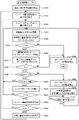
図1は、本発明の一実施例としての受電装置30を備える非接触送受電システム10の構成の概略を示す構成図である。実施例の非接触送受電システム10は、図1に示すように、駐車場などに設置された送電装置130と、送電装置130から非接触で受電可能な受電装置30を搭載する自動車20と、を備える。
FIG. 1 is a configuration diagram showing a schematic configuration of a contactless power transmission/
送電装置130は、家庭用電源(例えば、200V、50Hzなど)などの交流電源190に接続される送電ユニット131と、送電ユニット131を制御する送電用電子制御ユニット(以下、「送電ECU」という)170と、送電ECU170と通信すると共に自動車20の通信ユニット80(後述)と無線通信を行なう通信ユニット180と、を備える。
The
送電ユニット131は、AC/DCコンバータ132と、インバータ134と、フィルタ回路136と、送電用共振回路140と、を備える。AC/DCコンバータ132は、交流電源190からの交流電力を任意の電圧の直流電力に変換する周知のAC/DCコンバータとして構成されている。
The
インバータ134は、4つのスイッチング素子S11~S14と、4つのスイッチング素子S11~S14のそれぞれに逆方向に並列接続された4つのダイオードD11~D14と、を有する。スイッチング素子S11~S14としては、例えば、MOSFET(電界効果トランジスタの一種:metal-oxide-semiconductor field-effect transistor)が用いられる。スイッチング素子S11~S14は、AC/DCコンバータ132の出力側の正極側ラインおよび負極側ラインに対してソース側およびシンク側になるよう2個ずつペアで配置される。そして、2つのスイッチング素子S11,S12の接続点に設けられた(接続された)第1出力端子134a、および、2つのスイッチング素子S13,S14の接続点に設けられた(接続された)第2出力端子134bは、それぞれ、送電用共振回路140の送電用コイル141(後述)の一方側および他方側に接続された送電側第1ライン144aおよび送電側第2ライン144bに接続される。インバータ134は、送電ECU170によって、スイッチング素子S11~S14がパルス幅変調制御によりスイッチング制御されることにより、AC/DCコンバータ132からの直流電力を所望の周波数の交流電力に変換する。
The
フィルタ回路136は、ローパスフィルタとして構成されており、送電側第1ライン144aに設けられたコイル137と、送電側第1ライン144aにおけるコイル137よりも送電用共振回路140側(送電用コイル141側)と送電側第2ライン144bとに接続されたコンデンサ138と、を有する。このフィルタ回路136は、インバータ134からの交流電力の高周波ノイズを除去する。
The
送電用共振回路140は、例えば駐車場の床面などに設置された送電用コイル141と、送電用コイル141に直列に接続されたコンデンサ142と、を有する。この送電用共振回路140は、共振周波数が所定周波数Fset(数十~数百kHz程度)となるように設計されている。したがって、インバータ134では、基本的には、AC/DCコンバータ132からの直流電力を所定周波数Fsetの交流電力に変換する。
The power
送電ECU170は、図示しないが、CPUを中心とするマイクロプロセッサとして構成されており、CPUの他に、処理プログラムを記憶するROMや、データを一時的に記憶するRAM、入出力ポート、通信ポートを備える。送電ECU170には、各種センサからの信号が入力ポートを介して入力される。送電ECU170に入力される信号としては、例えば、AC/DCコンバータ132の出力側の両端子間に取り付けられた電圧センサ160からのAC/DCコンバータ132の出力電圧Vcoや、AC/DCコンバータ132とインバータ134との間の負極側ラインに取り付けられた電流センサ162からのAC/DCコンバータ132の出力電流Icoを挙げることができる。また、送電側第2ライン144bにおけるコンデンサ138との接続点よりもインバータ134側(第2出力端子134b側)に取り付けられた電流センサ163からのインバータ134の出力電流Iinや、送電側第2ライン144bにおけるコンデンサ138との接続点よりも送電用共振回路140側(送電用コイル141側)に取り付けられた電流センサ164からの送電用コイル141に流れる電流Itrも挙げることができる。送電ECU170からは、各種制御信号が出力ポートを介して出力される。送電ECU170から出力される信号としては、例えば、AC/DCコンバータ132への制御信号や、インバータ134のスイッチング素子S11~S14へのスイッチング制御信号を挙げることができる。
Although not shown, the
自動車20は、走行用のモータを備える電気自動車やハイブリッド自動車として構成されており、モータと電力をやりとりするバッテリ(電気負荷)22と、バッテリ22に接続される受電ユニット31と、車両全体を制御する車両用電子制御ユニット(以下、「車両ECU」という)70と、車両ECU70と通信すると共に送電装置130の通信ユニット180と無線通信を行なう通信ユニット80と、を備える。なお、実施例の「受電装置」としては、主として、受電ユニット31と車両ECU70と通信ユニット80とが該当する。
The
受電ユニット31は、受電用共振回路32と、フィルタ回路36と、倍電圧整流回路40と、平滑コンデンサ48と、を備える。受電用共振回路32は、例えば車体底面(フロアパネル)などに設置された受電用コイル33と、受電用コイル33に直列に接続されたコンデンサ(第1容量部)34と、を有する。受電用コイル33の一方側は、コンデンサ34および車両側第1ライン35aを介して倍電圧整流回路40の第1入力端子40aに接続され、他方側は、車両側第2ライン35bを介して倍電圧整流回路40の第2入力端子40bに接続される。この受電用共振回路32は、共振周波数が上述の所定周波数Fset(送電用共振回路140の共振周波数)付近の周波数(理想的には所定周波数Fset)となるように設計されている。
The
フィルタ回路36は、ローパスフィルタとして構成されており、車両側第1ライン35aに設けられたコイル37と、車両側第1ライン35aにおけるコイル37よりも受電用共振回路32側(受電用コイル33側)と車両側第2ライン35bとに接続されたコンデンサ38と、車両側第1ライン35aにおけるコイル37よりも倍電圧整流回路40側と車両側第2ライン35bとに接続されたコンデンサ39と、を有する。このフィルタ回路36は、受電用共振回路32により受電した交流電力の高周波ノイズを除去する。
The
倍電圧整流回路40は、ダイオードブリッジ回路42と、ダイオードブリッジ回路42に並列に接続された容量回路(第2容量部)44と、を有する。ダイオードブリッジ回路42は、4つのダイオードD21~D22を有する。4つのダイオードD21~D24は、バッテリ22に接続される正極側ラインおよび負極側ラインに対して2個ずつペアで直列に配置される。そして、2つのダイオードD21,D22の接続点に設けられた(接続された)第1入力端子40a、および、2つのダイオードD23,D24の接続点に設けられた(接続された)第2入力端子40bは、それぞれ、車両側第1ライン35aおよび車両側第2ライン35bに接続される。
The voltage
図2は、倍電圧整流回路40、特に、容量回路44の一例を示す構成図である。容量回路44は、図2に示すように、4つのコンデンサC21~C24と、スイッチS21と、を有する。4つのコンデンサC21~C24は、バッテリ22に接続される正極側ラインおよび負極ラインに対して2個ずつペアで直列に配置される。そして、2つのコンデンサC21,C22の接続点は、2つのダイオードD23,D24の接続点に接続される。スイッチS21は、車両ECU70によって制御され、2つのコンデンサC21,C22の接続点と、2つのコンデンサC21,C22の接続点と、の接続および接続の解除を行なう。
FIG. 2 is a configuration diagram showing an example of the voltage
この容量回路44では、スイッチS21がオフのときには、第2入力端子40bと正極側ラインとの間の容量(以下、「第1容量」という)Cd1は、コンデンサC21の容量となり、第2入力端子40bと負極側ラインとの間の容量(以下、「第2容量」という)Cd2は、コンデンサC22の容量となる。また、スイッチS21がオンのときには、第1容量値Cd1は、コンデンサC21,C23の容量の和となり、第2容量値Cd2は、コンデンサC22,C24の容量の和となる。なお、実施例では、コンデンサC21,C22は同一容量のものを用いるものとし、コンデンサC23,C24は同一容量のものを用いるものとした。したがって、スイッチS21がオフのときの第1,第2容量値Cd1,Cd2は、共に比較的小さい値Cdloとなり、スイッチS21がオンのときの第1,第2容量値Cd1,Cd2は、共に比較的大きい値Cdhiとなる。
In this
こうして構成される倍電圧整流回路40では、受電用共振回路32の受電用コイル33で受電した交流電力を整流かつ昇圧してバッテリ22に供給する。ダイオードブリッジ回路42および容量回路44を有する倍電圧整流回路40を用いることにより、ダイオードブリッジ回路42だけの(容量回路44を有しない)整流回路を用いる場合に比して、バッテリ22の電圧変動に対して安定して充電することができる。
The voltage
図1に示すように、平滑コンデンサ48は、倍電圧整流回路40よりもバッテリ22側で正極側ラインおよび負極側ラインに接続される。車両ECU70は、図示しないが、CPUを中心とするマイクロプロセッサとして構成されており、CPUの他に、処理プログラムを記憶するROMや、データを一時的に記憶するRAM、入出力ポート、通信ポートを備える。車両ECU70には、各種センサからの信号が入力ポートを介して入力される。車両ECU70に入力される信号としては、例えば、バッテリ22の両端子間に取り付けられた電圧センサ60からのバッテリ22の電圧Vbaや、車両側第2ライン35bにおけるコンデンサ38との接続点よりも受電用共振回路32側(受電用コイル33側)に取り付けられた電流センサ62からの受電用コイル33に流れる電流Ireを挙げることができる。また、車両側第2ライン35bにおけるコンデンサ38との接続点とコンデンサ39との接続点との間に取り付けられた電流センサ63からのフィルタ回路36に流れる電流Ifiや、バッテリ22の出力端子に取り付けられた電流センサ64からのバッテリ22の充放電電流Iba(バッテリ22を充電するときが正の値)も挙げることができる。車両ECU70からは、容量回路44のスイッチS21への制御信号などが出力ポートを介して出力される。車両ECU70は、バッテリ22の電圧Vbaおよび充放電電流Ibaの積としてバッテリ22の充電電力Pbaを演算したり、バッテリ22の充放電電流Ibaの積算値としてバッテリ22の蓄電割合SOCを演算したりする。
As shown in FIG. 1 , the smoothing
次に、こうして構成された非接触送受電システム10の動作、特に、送電装置130と受電装置30との非接触での送受電を伴ってバッテリ22を充電する非接触充電を行なう際の動作について説明する。なお、非接触充電は、受電装置30の受電用コイル33が送電装置130の送電用コイル141と略対向するように自動車20が駐車され、ユーザにより非接触充電の実行が指示されたときに行なわれる。図3は、送電ECU170により実行される送電側処理ルーチンの一例を示すフローチャートであり、図4は、車両ECU70により実行される車両側処理ルーチンの一例を示すフローチャートである。なお、図4のルーチンの開始時には、容量回路44のスイッチS21がオフであり、容量回路44の第1,第2容量値Cd1,Cd2が比較的小さい値Cdloになっている。
Next, the operation of the non-contact power transmission/
最初に、図3の送電側処理ルーチンについて説明する。本ルーチンが実行されると、送電ECU170は、車両ECU70との通信により各種データを取得し、車両情報や充電情報を照合する(ステップS100)。ここで、車両情報の照合では、例えば、自動車20が非接触充電を実行してよい車両であるか否かを判定する。また、充電情報の照合では、例えば、自動車20のバッテリ22の電圧Vbaに基づいてバッテリ22が満充電か否かを判定する。
First, the power transmission side processing routine in FIG. 3 will be described. When this routine is executed, the
続いて、インバータ134の駆動周波数(パルス幅変調制御における搬送波の周波数(キャリア周波数))fおよびデューティDにそれぞれ制御用の最小値fmin,Dminを設定する(ステップS110,S120)、ここで、最小値fminとしては、例えば、78kHzや79kHz、80kHzなどが用いられる。最小値Dminとしては、例えば、数%などが用いられる。 Subsequently, minimum values fmin and Dmin for control are set to the drive frequency (frequency of carrier wave (carrier frequency) in pulse width modulation control) f and duty D of inverter 134 (steps S110 and S120). As the value fmin, for example, 78 kHz, 79 kHz, 80 kHz, etc. are used. As the minimum value Dmin, for example, several percent is used.
そして、車両ECU70から通信によりバッテリ22の充電電力指令Psを受信し(ステップS130)、受信したバッテリ22の充電電力指令Psを許容充電電力指令Pslimで制限して(上限ガードして)バッテリ22の制御用充電電力指令Ps*を設定する(ステップS140)。ここで、許容充電電力指令Pslimは、本ルーチンの実行開始時には比較的大きい初期値が設定され、その後に後述のステップS250の処理が実行されると小さくなる。
Then, the charging power command Ps for the
こうしてバッテリ22の制御用充電電力指令Ps*を設定すると、設定した制御用充電電力指令Ps*が正か値0かを判定し(ステップS150)、制御用充電電力指令Ps*が正のときには、送電装置130から受電装置30に給電すると判断し、制御用充電電力指令Ps*やインバータ134の駆動周波数fおよびデューティDを用いて、AC/DCコンバータ132およびインバータ134を駆動制御する(ステップS160)。
After setting the control charging power command Ps* for the
次に、車両ECU70から通信によりバッテリ22の電圧Vbaや充電電力Pba、エラー情報フラグFを受信する(ステップS170)。エラー情報フラグFは、車両ECU70により、自動車20でエラー(異常)が生じていないときには値0が設定され、エラーが生じたときには値1が設定されるフラグである。
Next, the voltage Vba of the
そして、エラー情報フラグFの値を調べ(ステップS180)、エラー情報フラグFが値0のときには、自動車20でエラーが生じていないと判断し、バッテリ22の電圧Vbaの今回値が閾値Vref以上で且つ前回値が閾値Vref未満か否かを判定する(ステップS190)。ここで、閾値Vrefは、例えば、バッテリ22の満充電電圧Vflよりも数十V程度低い値が用いられる。ステップS190の処理は、バッテリ22の電圧Vbaが閾値Vref以上に至った直後であるか否かを判定する処理である。
Then, the value of the error information flag F is checked (step S180), and when the error information flag F is 0, it is determined that no error has occurred in the
ステップS190で、バッテリ22の電圧Vbaの今回値が閾値Vref以上のときや前回値が閾値Vref未満のときには、バッテリ22の電圧Vbaが閾値Vref以上に至った直後でないと判断し、バッテリ22の制御用充電電力指令Ps*と充電電力Pbaとが乖離しているか否かを判定する(ステップS200)。この判定は、例えば、バッテリ22の制御用充電電力指令Ps*と充電電力Pbaとの差分を閾値と比較することにより行なわれる。バッテリ22の制御用充電電力指令Ps*と充電電力Pbaとが乖離していないときには、ステップS130に戻る。
In step S190, when the current value of the voltage Vba of the
ステップS200でバッテリ22の制御用充電電力指令Ps*と充電電力Pbaとが乖離しているときには、インバータ134のデューティDを所定値ΔDだけ増加させて更新し(ステップS210)、更新後のデューティDを許容デューティDlimと比較する(ステップS220)。ここで、所定値ΔDは、インバータ134の仕様などに基づいて予め解析などにより設定される。許容デューティDlimとしては、例えば、50%が用いられる。インバータ134のデューティDが許容デューティDlim以下のときには、デュ-ティDは許容範囲内であると判断し、ステップS130に戻る。
When there is a discrepancy between the charging power command Ps* for control of the
ステップS220でインバータ134のデューティDが許容デューティDlimよりも大きいときには、インバータ134の駆動周波数fを所定値Δfだけ増加させて更新し(ステップS230)、更新後の駆動周波数fを許容周波数flimと比較する(ステップS240)。ここで、所定値Δfは、インバータ134の仕様などに基づいて予め解析などにより設定される。許容周波数flimとしては、例えば、89kHzや90kHz、91kHzなどが用いられる。
When the duty D of the
ステップS240でインバータ134の駆動周波数fが許容周波数flim以下のときには、ステップS120に戻る。一方、インバータ134の駆動周波数fが許容周波数flimよりも大きいときには、許容充電電力指令Pslimを所定値ΔPsだけ低下させて(ステップS250)、ステップS110に戻る。ここで、所定値ΔPsは、送電装置130の仕様などに基づいて予め解析などにより設定される。
When the drive frequency f of the
ステップS190で、バッテリ22の電圧Vbaの今回値が閾値Vref以上で且つ前回値が閾値Vref未満のときには、バッテリ22の電圧Vbaが閾値Vref以上に至った直後であると判断し、AC/DCコンバータ132およびインバータ134を駆動停止し(ステップS260)、容量回路44の第1,第2容量値Cd1,Cd2の切替を車両ECU70に要請する(ステップS270)。そして、容量回路44の第1,第2容量値Cd1,Cd2の切替を行なったことを示す切替完了信号を車両ECU70から受信するのを待って(ステップS280)、ステップS130に戻る。即ち、車両ECU70により容量回路44の第1,第2容量値Cd1,Cd2の切替が行なわれる際には、AC/DCコンバータ132およびインバータ134を駆動停止することにより、非接触充電を停止させるのである。これにより、非接触充電を中断して容量回路44の第1,第2容量値Cd1,Cd2を切り替えることができるから、容量回路44の保護を図ることができる。なお、この駆動停止時間は、非接触充電の時間(例えば、数時間程度)に比して十分に短い時間である。
In step S190, when the current value of the voltage Vba of the
ステップS150で制御用充電電力指令Ps*が値0のときには、送電装置130から受電装置30に給電しないと判断し、AC/DCコンバータ132およびインバータ134を駆動停止して(ステップS290)、本ルーチンを終了する。これにより、送電装置130と受電装置30との非接触での送受電が終了し、非接触充電が終了する。
When the control charge power command Ps* is 0 in step S150, it is determined that
ステップS180でエラー情報フラグFが値1のときには、自動車20でエラーが生じていると判断し、バッテリ22の制御用充電電力指令Ps*に拘わらずに、AC/DCコンバータ132およびインバータ134を駆動停止して(ステップS290)、本ルーチンを終了する。これにより、送電装置130と受電装置30との非接触での送受電が終了し、非接触充電が終了する。
When the error information flag F is 1 in step S180, it is determined that an error has occurred in the
次に、図4の車両側処理ルーチンについて説明する。本ルーチンが実行されると、車両ECU70は、車両情報や充電情報を照合する(ステップS300)。車両情報や充電情報の照合は、上述のステップS100の処理と同様に行なわれる。
Next, the vehicle-side processing routine of FIG. 4 will be described. When this routine is executed, the
続いて、送電ECU170により容量回路44の第1,第2容量値Cd1,Cd2の切替が要請されているか否かを判定し(ステップS310)、第1,第2容量値Cd1,Cd2の切替が要請されていないときには、バッテリ22の電圧Vbaを満充電電圧Vflと比較する(ステップS340)。
Subsequently, it is determined whether switching of the first and second capacitance values Cd1 and Cd2 of the
そして、バッテリ22の電圧Vbaを満充電電圧Vfl未満のときには、バッテリ22の充電電力指令Psを設定する(ステップS350)。ここで、バッテリ22の充電電力指令Psは、例えば、バッテリ22の充電電力Pbaが小さいほど大きくなるように設定される。バッテリ22の充電電力Pbaが小さいほど(バッテリ22の充電電力指令Psと充電電力Pbとの差分が大きいほど)、自動車20の車高が高かったり自動車20に搭載される送電用コイル141の位置が非接触充電に最適の位置(受電用コイル33と十分に対向する位置)からずれていたりするなどの理由により、送電用コイル141と受電用コイル33との結合係数が低くなると考えられるためである。
Then, when the voltage Vba of the
次に、各種センサからバッテリ22の電圧Vbaや充放電電流Iba、受電用コイル33に流れる電流Ire、フィルタ回路36に流れる電流Ifiを入力し(ステップS360)、入力したバッテリ22の電圧Vbaや充放電電流Iba、受電用コイル33に流れる電流Ire、フィルタ回路36に流れる電流Ifiの全てが許容範囲内か否かを判定する(ステップS370)。
Next, the voltage Vba of the
バッテリ22の電圧Vbaや充放電電流Iba、受電用コイル33に流れる電流Ire、フィルタ回路36に流れる電流Ifiの全てが許容範囲内のときには、自動車20にエラーは生じていないと判断し、エラー情報フラグFに値0を設定し(ステップS380)、バッテリ22の電圧Vbaと充放電電流Ibaとの積としてバッテリ22の充電電力Pbaを演算し(ステップS390)、エラー情報フラグFおよびバッテリ22の充電電力Pbaを充電情報として送電ECU170に送信して(ステップS410)、ステップS310に戻る。
When the voltage Vba of the
ステップS370でバッテリ22の電圧Vbaや充放電電流Iba、受電用コイル33に流れる電流Ire、フィルタ回路36に流れる電流Ifiのうちの少なくとも1つが許容範囲外のときには、自動車20にエラー生じたと判断し、エラー情報フラグFに値1を設定し(ステップS400)、エラー情報フラグFを充電情報として送電ECU170に送信して(ステップS410)、ステップS310に戻る。送電ECU170は、値1のエラー情報フラグFを受信すると、上述したように、AC/DCコンバータ132およびインバータ134を駆動停止する(ステップS290)。これにより、送電装置130と受電装置30との非接触での送受電が終了し、非接触充電が終了する。
If at least one of the voltage Vba of the
ステップS320で送電ECU170により容量回路44の第1,第2容量値Cd1,Cd2の切替が要請されているときには、容量回路44の第1,第2容量値Cd1,Cd2を比較的小さい値Cdloから比較的大きい値Cdhiに切り替える(ステップS320)。この切替は、スイッチS21をオフからオンにすることにより行なわれる。そして、この切替が完了すると、切替完了信号を送電ECU170に送信して(ステップS330)、ステップS340以降の処理を実行する。なお、上述したように、容量回路44の第1,第2容量値Cd1,Cd2を切り替える際には、送電装置130のAC/DCコンバータ132およびインバータ134が駆動停止されることにより非接触充電が中断されるから、容量回路44の保護を図ることができる。
When the
ステップS340でバッテリ22の電圧Vbaが満充電電圧Vfl以上のときには、バッテリ22の非接触充電を終了すると判断し、バッテリ22の充電電力指令Psに値0を設定して(ステップS430)、本ルーチンを終了する。送電ECU170は、値0の充電電力指令Psを受信すると、上述したように、AC/DCコンバータ132およびインバータ134を駆動停止する(ステップS290)。これにより、送電装置130と受電装置30との非接触での送受電が終了し、非接触充電が終了する。
When the voltage Vba of the
即ち、実施例では、非接触充電の開始時には、車両ECU70は、容量回路44の第1,第2容量値Cd1,Cd2を比較的小さい値Cdloとする。そして、バッテリ22の電圧Vbaが閾値Vref以上に至って送電ECU170が車両ECU70に容量回路44の第1,第2容量値Cd1,Cd2の切替を要請すると、車両ECU70は、容量回路44の第1,第2容量値Cd1,Cd2を比較的大きい値Cdhiに切り替える。以下、その理由について説明する。
That is, in the embodiment, at the start of non-contact charging, the
図5は、容量回路44の第1,第2容量値Cd1,Cd2を2段階(値Cdlo,Cdhi)でなく任意に変更できると仮定したときの、第1,第2容量値Cd1,Cd2と送電用コイル141の力率との関係についての一例を示す説明図である。図6は、図5と同様に仮定したときの、第1,第2容量値Cd1,Cd2と受電装置30の力率との関係の一例を示す説明図である。図5および図6では、値Cdlo,Cdhiについても図示した。図5に示すように、第1,第2容量値Cd1,Cd2が低いほど送電用コイル141の力率が高くなり、図6に示すように、第1,第2容量値Cd1,Cd2が低いほど受電装置30の力率が高くなる(効率が良くなる)。これらの傾向は、本発明者らが解析などにより確認したものである。こうした傾向から、第1,第2容量値Cd1,Cd2を低くすると、非接触充電を行なう際の充電効率を良好にすることができると言える。
FIG. 5 shows the first and second capacitance values Cd1 and Cd2 when it is assumed that the first and second capacitance values Cd1 and Cd2 of the
バッテリ22の電圧が低いときには、高いときに比して、受電用コイル33の出力側(バッテリ22側)のインピーダンスが大きいことから、バッテリ22を比較的大きい電力で充電するためには、送電用コイル141に流す電流Itrを大きくする必要がある。送電用コイル141に流す電流が大きくなると、送電用コイル141の銅損が大きくなり、非接触充電を行なう際の充電効率が低下しやすくなる。
When the voltage of the
これらのことを考慮して、実施例では、車両ECU70は、非接触充電の開始時には、容量回路44の第1,第2容量値Cd1,Cd2を比較的小さい値Cdloとし、非接触充電の継続によりバッテリ22の電圧Vbaが上昇して閾値Vref以上に至ると、容量回路44の第1,第2容量値Cd1,Cd2を比較的大きい値Cdhiに切り替えるものとした。これにより、バッテリ22の電圧Vbaに拘わらずに容量回路44の第1,第2容量値Cd1,Cd2を比較的大きい値Cdhiとするものに比して、バッテリ22の電圧Vbaが閾値Vref未満のときに、送電用コイル141や受電装置30の力率を良好にして、充電効率を良好にすることができる。なお、バッテリ22の電圧Vbaが高いときには、送電用コイル141に流す電流をそれほど大きくしなくてよいから、送電用コイル141の銅損がそれほど大きくならない。したがって、このときには、容量回路44の第1,第2容量値Cd1,Cd2を比較的大きい値Cdhiとすることにより、比較的小さい値Cdloで保持するものに比して、バッテリ22の電圧変動に対して安定して充電することができる。
In consideration of these, in the embodiment, the
図7は、実施例と比較例とで送電用コイル141に流す電流を同一にしたときの、実施例および比較例のバッテリ22の電圧Vbaと充電電力Pbaとの関係の一例を示す説明図である。図中、実線は実施例を示し、一点鎖線は比較例を示す。比較例では、バッテリ22の電圧Vbaに拘わらずに容量回路44の第1,第2容量値Cd1,Cd2を比較的大きい値Cdhiとした。図7の傾向(様子)は、本発明者らが解析などにより確認したものである。図7に示すように、バッテリ22の電圧Vbaが閾値Vref未満の領域で、実施例が比較例に比してバッテリ22の充電電力Pbaが大きくなっていることが解る。
FIG. 7 is an explanatory diagram showing an example of the relationship between the voltage Vba and the charging power Pba of the
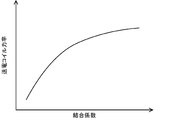
図8は、送電装置130の送電用コイル141と受電装置30の受電用コイル33との結合係数と、送電用コイル141の力率と、の関係の一例を示す説明図である。図9は、この結合係数と、バッテリ22を比較的大きい電力で充電するために送電用コイル141に流すべき電流と、の関係の一例を示す説明図である。図8に示すように、結合係数が低いほど送電用コイル141の力率が低くなる。この傾向は、本発明者らが解析などにより確認したものである。この図8の傾向を踏まえると、バッテリ22に比較的大きい電力で充電するためには、図9に示すように、結合係数が低いほど送電用コイル141に流すべき電流を大きくする必要がある。したがって、結合係数が低いときには、送電用コイル141の銅損がより大きくなるから、本発明を実施することの意義がより大きくなる。
FIG. 8 is an explanatory diagram showing an example of the relationship between the coupling coefficient between the
以上説明した実施例の受電装置30では、非接触充電の開始時には、容量回路44の第1,第2容量値Cd1,Cd2を比較的小さい値Cdloとし、非接触充電の継続によりバッテリ22の電圧Vbaが上昇して閾値Vref以上に至ると、容量回路44の第1,第2容量値Cd1,Cd2を比較的大きい値Cdhiに切り替える。これにより、バッテリ22の電圧Vbaに拘わらずに容量回路44の第1,第2容量値Cd1,Cd2を比較的大きい値Cdhiとするものに比して、バッテリ22の電圧Vbaが閾値Vref未満のときの充電効率を良好にすることができる。
In the
また、実施例の送電装置130では、受電装置30の容量回路44の第1,第2容量値Cd1,Cd2を切り替える際には、AC/DCコンバータ132およびインバータ134を駆動停止する。これにより、非接触充電が中断されるから、容量回路44の保護を図ることができる。
Further, in the
実施例の主要な要素と課題を解決するための手段の欄に記載した発明の主要な要素との対応関係について説明する。実施例では、受電用コイル33およびコンデンサ34を有する受電用共振回路32が「受電用共振回路」に相当し、ダイオードブリッジ回路42および容量回路44を有する倍電圧整流回路40が「倍電圧整流回路」に相当し、車両ECU70が「制御部」に相当する。
The correspondence relationship between the main elements of the embodiments and the main elements of the invention described in the column of Means for Solving the Problems will be described. In the embodiment, the power receiving
なお、実施例の主要な要素と課題を解決するための手段の欄に記載した発明の主要な要素との対応関係は、実施例が課題を解決するための手段の欄に記載した発明を実施するための形態を具体的に説明するための一例であることから、課題を解決するための手段の欄に記載した発明の要素を限定するものではない。即ち、課題を解決するための手段の欄に記載した発明についての解釈はその欄の記載に基づいて行なわれるべきものであり、実施例は課題を解決するための手段の欄に記載した発明の具体的な一例に過ぎないものである。 Note that the correspondence relationship between the main elements of the examples and the main elements of the invention described in the column of Means for Solving the Problems is the Since it is an example for specifically explaining the mode for solving the problem, it does not limit the elements of the invention described in the column of the means for solving the problem. That is, the interpretation of the invention described in the column of Means to Solve the Problem should be made based on the description in that column, and the Examples are based on the description of the invention described in the column of Means to Solve the Problem. This is only a specific example.
以上、本発明を実施するための形態について実施例を用いて説明したが、本発明はこうした実施例に何等限定されるものではなく、本発明の要旨を逸脱しない範囲内において、種々なる形態で実施し得ることは勿論である。 Although the embodiments for carrying out the present invention have been described above, the present invention is not limited to such embodiments at all, and can be modified in various forms without departing from the scope of the present invention. Of course, it can be implemented.
本発明は、受電装置の製造産業などに利用可能である。 INDUSTRIAL APPLICABILITY The present invention can be used in the power receiving device manufacturing industry and the like.
10 非接触送受電システム、20 自動車、22 バッテリ、30 受電装置、31 受電ユニット、32 受電用共振回路、33 受電用コイル、34 コンデンサ(第1容量部)、35a 車両側第1ライン、35b 車両側第2ライン、36 フィルタ回路、37 コイル、38,39 コンデンサ、40 倍電圧整流回路、40a 第1入力端子、40b 第2入力端子、42 ダイオードブリッジ回路、44 容量回路(第2容量部)、48 平滑コンデンサ、60 電圧センサ、62,63,64 電流センサ、70 車両ECU、80 通信ユニット、130 送電装置、131 送電ユニット、132 AC/DCコンバータ、134 インバータ、134a 第1出力端子、134b 第2出力端子、136 フィルタ回路、137 コイル、138 コンデンサ、140 送電用共振回路、141 送電用コイル、142 コンデンサ、144a 送電側第1ライン、144b 送電側第2ライン、160 電圧センサ、162,163,164 電流センサ、170 送電ECU、80、180 通信ユニット、190 交流電源、C21~C24 コンデンサ、D11~D14,D21~D24 ダイオード、S11~S14 スイッチング素子、S21 スイッチ。
REFERENCE SIGNS
Claims (1)
前記送電装置は、前記送電用コイルを有する送電ユニットと、前記送電ユニットを制御する送電側制御部とを備え、
前記受電装置は、
前記送電用コイルから非接触で受電可能な受電用コイル、および、前記受電用コイルに接続された第1容量部を有する受電用共振回路と、
前記受電用共振回路に接続されるダイオードブリッジ回路、および、前記ダイオードブリッジ回路に並列に接続されると共に容量が可変の第2容量部を有し、前記受電用共振回路からの電力を整流かつ昇圧して前記電気負荷に供給する倍電圧整流回路と、
前記電気負荷の電圧が所定電圧未満のときには、前記電気負荷の電圧が前記所定電圧以上のときに比して前記第2容量部の容量値を小さい値に制御する制御部と、
を備え、
前記送電側制御部は、前記電気負荷の電圧が前記所定電圧未満から前記所定電圧以上に上昇して前記受電装置で前記第2容量部の容量値を大きくする際には、前記送電用コイルと前記受電用コイルとの送受電が中断されるように前記送電ユニットを制御する、
非接触送受電システム。 A contactless power transmission/reception system comprising: a power transmission device; and a power reception device that supplies power received from the power transmission device in a contactless manner to an electrical load,
The power transmission device includes a power transmission unit having the power transmission coil, and a power transmission side control section that controls the power transmission unit,
The power receiving device
a power receiving coil capable of contactlessly receiving power from the power transmitting coil; and a power receiving resonance circuit including a first capacitor connected to the power receiving coil;
A diode bridge circuit connected to the power receiving resonance circuit, and a second capacitor unit connected in parallel to the diode bridge circuit and having a variable capacitance, which rectifies and boosts the power from the power receiving resonance circuit. and a voltage doubler rectifier circuit for supplying to the electrical load;
a control unit that controls the capacitance value of the second capacitance unit to be smaller when the voltage of the electric load is less than a predetermined voltage compared to when the voltage of the electric load is equal to or higher than the predetermined voltage;
with
When the voltage of the electrical load rises from less than the predetermined voltage to the predetermined voltage or more and the power receiving device increases the capacitance value of the second capacitance unit, the power transmission side control unit controls the power transmission coil and controlling the power transmission unit such that power transmission and reception with the power receiving coil is interrupted;
Contactless power transmission and reception system .
Priority Applications (1)
| Application Number | Priority Date | Filing Date | Title |
|---|---|---|---|
| JP2018196438A JP7140629B2 (en) | 2018-10-18 | 2018-10-18 | Contactless power transmission/reception system |
Applications Claiming Priority (1)
| Application Number | Priority Date | Filing Date | Title |
|---|---|---|---|
| JP2018196438A JP7140629B2 (en) | 2018-10-18 | 2018-10-18 | Contactless power transmission/reception system |
Publications (3)
| Publication Number | Publication Date |
|---|---|
| JP2020065391A JP2020065391A (en) | 2020-04-23 |
| JP2020065391A5 JP2020065391A5 (en) | 2021-06-17 |
| JP7140629B2 true JP7140629B2 (en) | 2022-09-21 |
Family
ID=70387663
Family Applications (1)
| Application Number | Title | Priority Date | Filing Date |
|---|---|---|---|
| JP2018196438A Active JP7140629B2 (en) | 2018-10-18 | 2018-10-18 | Contactless power transmission/reception system |
Country Status (1)
| Country | Link |
|---|---|
| JP (1) | JP7140629B2 (en) |
Cited By (1)
| Publication number | Priority date | Publication date | Assignee | Title |
|---|---|---|---|---|
| US20220103058A1 (en) * | 2020-09-30 | 2022-03-31 | Solaredge Technologies Ltd. | Method and Apparatus for Power Conversion |
Citations (3)
| Publication number | Priority date | Publication date | Assignee | Title |
|---|---|---|---|---|
| JP2005295759A (en) | 2004-04-05 | 2005-10-20 | Matsushita Electric Ind Co Ltd | Power supply for air conditioner |
| JP5011046B2 (en) | 2007-09-25 | 2012-08-29 | 株式会社キトー | Wet friction plate |
| JP2017184363A (en) | 2016-03-29 | 2017-10-05 | 株式会社Soken | Non-contact power reception device |
Family Cites Families (3)
| Publication number | Priority date | Publication date | Assignee | Title |
|---|---|---|---|---|
| JPS5011046B1 (en) * | 1968-02-29 | 1975-04-26 | ||
| JPH11289766A (en) * | 1998-04-03 | 1999-10-19 | Toshiba Ave Co Ltd | Power supply |
| JP2016082707A (en) * | 2014-10-16 | 2016-05-16 | 株式会社日本自動車部品総合研究所 | Power receiving device and power transmitting device |
-
2018
- 2018-10-18 JP JP2018196438A patent/JP7140629B2/en active Active
Patent Citations (3)
| Publication number | Priority date | Publication date | Assignee | Title |
|---|---|---|---|---|
| JP2005295759A (en) | 2004-04-05 | 2005-10-20 | Matsushita Electric Ind Co Ltd | Power supply for air conditioner |
| JP5011046B2 (en) | 2007-09-25 | 2012-08-29 | 株式会社キトー | Wet friction plate |
| JP2017184363A (en) | 2016-03-29 | 2017-10-05 | 株式会社Soken | Non-contact power reception device |
Cited By (2)
| Publication number | Priority date | Publication date | Assignee | Title |
|---|---|---|---|---|
| US20220103058A1 (en) * | 2020-09-30 | 2022-03-31 | Solaredge Technologies Ltd. | Method and Apparatus for Power Conversion |
| US11770063B2 (en) * | 2020-09-30 | 2023-09-26 | Solaredge Technologies Ltd. | Power inverter with voltage control circuitry |
Also Published As
| Publication number | Publication date |
|---|---|
| JP2020065391A (en) | 2020-04-23 |
Similar Documents
| Publication | Publication Date | Title |
|---|---|---|
| CA2932518C (en) | Non-contact electric power transmitting device and electric power transfer system | |
| CN108400641B (en) | Non-contact power transmission device | |
| US10277082B2 (en) | Power-transmitting device and wireless power-supplying system | |
| JP6323346B2 (en) | Power transmission equipment | |
| JP2019140775A (en) | On-vehicle charger and control method of on-vehicle charger | |
| EP3280029A1 (en) | Contactless power supply device, program, method for controlling contactless power supply device, and contactless power transmission system | |
| JP2016134969A (en) | Power supply control apparatus | |
| EP3270487B1 (en) | Non-contact power supply apparatus, program, method for controlling non-contact power supply apparatus, and non-contact power transmission system | |
| JP7048473B2 (en) | Power receiving device | |
| CN106374631B (en) | Non-contact power transmission device and electrical power transmission system | |
| CN107026514B (en) | Power transmission device and power transmission system | |
| JP7140629B2 (en) | Contactless power transmission/reception system | |
| WO2020241405A1 (en) | In-motion power supply system | |
| CN113676044A (en) | Power supply circuit control device, control method, and recording medium storing program | |
| KR20190084681A (en) | Method of efficiently controlling battery chargers and a battery charger adopting the same | |
| RU2625167C2 (en) | Electrical power transmitting device | |
| JP2014110666A (en) | Discharge control system, and discharge device | |
| JP6798953B2 (en) | Power supply system | |
| JP2016127647A (en) | Power transmission device | |
| JP2015216739A (en) | Power transmission apparatus | |
| JP2019213267A (en) | Non-contact transmission apparatus | |
| JP6803818B2 (en) | Power supply system | |
| JP6390179B2 (en) | Power supply vehicle, charging system, and charging method | |
| JP2018099001A (en) | Transmission equipment | |
| JP6974244B2 (en) | Contactless power transmission device |
Legal Events
| Date | Code | Title | Description |
|---|---|---|---|
| A521 | Request for written amendment filed |
Free format text: JAPANESE INTERMEDIATE CODE: A523 Effective date: 20210423 |
|
| A621 | Written request for application examination |
Free format text: JAPANESE INTERMEDIATE CODE: A621 Effective date: 20210423 |
|
| A131 | Notification of reasons for refusal |
Free format text: JAPANESE INTERMEDIATE CODE: A131 Effective date: 20220222 |
|
| A521 | Request for written amendment filed |
Free format text: JAPANESE INTERMEDIATE CODE: A523 Effective date: 20220329 |
|
| TRDD | Decision of grant or rejection written | ||
| A01 | Written decision to grant a patent or to grant a registration (utility model) |
Free format text: JAPANESE INTERMEDIATE CODE: A01 Effective date: 20220816 |
|
| A61 | First payment of annual fees (during grant procedure) |
Free format text: JAPANESE INTERMEDIATE CODE: A61 Effective date: 20220908 |
|
| R150 | Certificate of patent or registration of utility model |
Ref document number: 7140629 Country of ref document: JP Free format text: JAPANESE INTERMEDIATE CODE: R150 |