JP7130542B2 - Partial discharge detection device and partial discharge detection method - Google Patents
Partial discharge detection device and partial discharge detection method Download PDFInfo
- Publication number
- JP7130542B2 JP7130542B2 JP2018232934A JP2018232934A JP7130542B2 JP 7130542 B2 JP7130542 B2 JP 7130542B2 JP 2018232934 A JP2018232934 A JP 2018232934A JP 2018232934 A JP2018232934 A JP 2018232934A JP 7130542 B2 JP7130542 B2 JP 7130542B2
- Authority
- JP
- Japan
- Prior art keywords
- partial discharge
- converter
- digital signal
- sampling frequency
- waveform
- Prior art date
- Legal status (The legal status is an assumption and is not a legal conclusion. Google has not performed a legal analysis and makes no representation as to the accuracy of the status listed.)
- Active
Links
Images


Classifications
-
- G—PHYSICS
- G01—MEASURING; TESTING
- G01R—MEASURING ELECTRIC VARIABLES; MEASURING MAGNETIC VARIABLES
- G01R31/00—Arrangements for testing electric properties; Arrangements for locating electric faults; Arrangements for electrical testing characterised by what is being tested not provided for elsewhere
- G01R31/12—Testing dielectric strength or breakdown voltage ; Testing or monitoring effectiveness or level of insulation, e.g. of a cable or of an apparatus, for example using partial discharge measurements; Electrostatic testing
- G01R31/1227—Testing dielectric strength or breakdown voltage ; Testing or monitoring effectiveness or level of insulation, e.g. of a cable or of an apparatus, for example using partial discharge measurements; Electrostatic testing of components, parts or materials
- G01R31/1263—Testing dielectric strength or breakdown voltage ; Testing or monitoring effectiveness or level of insulation, e.g. of a cable or of an apparatus, for example using partial discharge measurements; Electrostatic testing of components, parts or materials of solid or fluid materials, e.g. insulation films, bulk material; of semiconductors or LV electronic components or parts; of cable, line or wire insulation
- G01R31/1272—Testing dielectric strength or breakdown voltage ; Testing or monitoring effectiveness or level of insulation, e.g. of a cable or of an apparatus, for example using partial discharge measurements; Electrostatic testing of components, parts or materials of solid or fluid materials, e.g. insulation films, bulk material; of semiconductors or LV electronic components or parts; of cable, line or wire insulation of cable, line or wire insulation, e.g. using partial discharge measurements
-
- G—PHYSICS
- G01—MEASURING; TESTING
- G01R—MEASURING ELECTRIC VARIABLES; MEASURING MAGNETIC VARIABLES
- G01R19/00—Arrangements for measuring currents or voltages or for indicating presence or sign thereof
- G01R19/25—Arrangements for measuring currents or voltages or for indicating presence or sign thereof using digital measurement techniques
- G01R19/2506—Arrangements for conditioning or analysing measured signals, e.g. for indicating peak values ; Details concerning sampling, digitizing or waveform capturing
- G01R19/2509—Details concerning sampling, digitizing or waveform capturing
-
- G—PHYSICS
- G01—MEASURING; TESTING
- G01R—MEASURING ELECTRIC VARIABLES; MEASURING MAGNETIC VARIABLES
- G01R31/00—Arrangements for testing electric properties; Arrangements for locating electric faults; Arrangements for electrical testing characterised by what is being tested not provided for elsewhere
- G01R31/50—Testing of electric apparatus, lines, cables or components for short-circuits, continuity, leakage current or incorrect line connections
- G01R31/52—Testing for short-circuits, leakage current or ground faults
-
- G—PHYSICS
- G01—MEASURING; TESTING
- G01R—MEASURING ELECTRIC VARIABLES; MEASURING MAGNETIC VARIABLES
- G01R31/00—Arrangements for testing electric properties; Arrangements for locating electric faults; Arrangements for electrical testing characterised by what is being tested not provided for elsewhere
- G01R31/12—Testing dielectric strength or breakdown voltage ; Testing or monitoring effectiveness or level of insulation, e.g. of a cable or of an apparatus, for example using partial discharge measurements; Electrostatic testing
- G01R31/14—Circuits therefor, e.g. for generating test voltages, sensing circuits
Description
本発明は、部分放電検出装置及び部分放電検出方法に関する。 The present invention relates to a partial discharge detection device and a partial discharge detection method.
電力ケーブルの絶縁劣化の兆候を観測するには、電力ケーブルの絶縁物に高電圧を印加した際に発生する、部分放電の電荷量を測定することが一般的である。電力ケーブルの中間接続箱には、ケーブルの絶縁物と接続された接地線がある。部分放電事象発生時に接地線に流れる電流を、電流測定器(CT:Current Transformer)で測定することが可能である。そして、電流測定器が測定した部分放電発生時の電流は、AD(Analog-to-Digital)変換によりデジタル値に変換され、ケーブルに流れる交流波形の位相に応じて、部分放電の電流が評価される。 In order to observe signs of insulation deterioration of a power cable, it is common to measure the charge amount of partial discharge that occurs when a high voltage is applied to the insulator of the power cable. The power cable junction box has a ground wire connected to the cable insulation. The current flowing in the ground wire during a partial discharge event can be measured with a Current Transformer (CT). Then, the current measured by the current measuring device at the time of occurrence of partial discharge is converted into a digital value by AD (Analog-to-Digital) conversion, and the current of partial discharge is evaluated according to the phase of the AC waveform flowing through the cable. be.
例えば、特許文献1には、ケーブルの絶縁物に高電圧を印加した際に発生する部分放電の電荷量を測定することで、ケーブルの絶縁劣化の兆候を観測する技術が開示されている。
For example,
電流測定器が測定した部分放電の放電パルスはアナログ信号であるため、AD変換器でアナログ信号をデジタル化する必要がある。部分放電は、微小間隔で発生する高周波パルスのアナログ波形で観測されるため、部分放電の放電パルスを広範囲な周波数帯域で測定することが求められる。また、AD変換器は、サンプリング定理を満たすように動作することが必要である。 Since the discharge pulse of partial discharge measured by the current measuring device is an analog signal, it is necessary to digitize the analog signal with an AD converter. Since partial discharge is observed as an analog waveform of high-frequency pulses generated at minute intervals, it is required to measure discharge pulses of partial discharge in a wide frequency band. Also, the AD converter must operate so as to satisfy the sampling theorem.
しかし、サンプリング定理を満たす条件で、広範囲な周波数帯域のアナログ信号をAD変換器がデジタル化して測定するには、超高速サンプリングが必要となる。超高速サンプリングが可能なAD変換器は非常に高価であり、また、AD変換したデジタルデータも超高速で出力されることとなる。この場合、デジタルデータの信号処理も超高速化が要求される。また、信号処理を実施するFPGA(Field Programmable Gate Array)には、超高速で行われる信号処理に対応するため、高速かつ高価なものが使用される。よって、部分放電パルスを測定するためのハードウェアが高価になってしまう。 However, under the condition that the sampling theorem is satisfied, ultra-high-speed sampling is required in order for an AD converter to digitize and measure analog signals in a wide frequency band. AD converters capable of ultra-high-speed sampling are very expensive, and AD-converted digital data is also output at ultra-high speed. In this case, ultra-high-speed digital data signal processing is also required. Also, a high-speed and expensive FPGA is used for the FPGA (Field Programmable Gate Array) that performs signal processing in order to cope with signal processing performed at ultra-high speed. Therefore, the hardware for measuring partial discharge pulses becomes expensive.
そこで、広帯域で発生する部分放電パルスを検出するAD変換器として、サンプリング定理を満たさない条件で、超高速に動作しないAD変換器を採用することが発明者により検討された。サンプリング定理を満たさない条件でアナログ信号をAD変換すると、第1、第2、第3、…、第nナイキストの全ナイキストの周波数帯域に、部分放電パルスが折返しノイズで観測される。部分放電パルスの有無を確認するだけでよければ、折返しノイズが観測されても問題ない。 Therefore, the inventors have considered adopting an AD converter that does not operate at ultra high speed under conditions that do not satisfy the sampling theorem as an AD converter for detecting partial discharge pulses generated in a wide band. When an analog signal is AD-converted under a condition that does not satisfy the sampling theorem, partial discharge pulses are observed as aliasing noise in all Nyquist frequency bands of the first, second, third, . . . , n-th Nyquist. If it is only necessary to confirm the presence or absence of partial discharge pulses, there is no problem even if aliasing noise is observed.
しかし、サンプリング定理を満たさない条件で行われるAD変換は、第1、第2、第3、…、第nナイキスト境界の周波数帯域におけるSN比(Signal-to-Noise ratio)が著しく悪くなる。仮に、部分放電パルスの周波数帯域がナイキストの境界であった場合、SN比が悪くなるため、部分放電パルスを観測できなかった。 However, AD conversion performed under conditions that do not satisfy the sampling theorem significantly deteriorates the SN ratio (Signal-to-Noise ratio) in the frequency bands of the first, second, third, . . . , n-th Nyquist boundaries. If the frequency band of the partial discharge pulse was on the Nyquist boundary, the SN ratio would deteriorate, so the partial discharge pulse could not be observed.
本発明はこのような状況に鑑みて成されたものであり、広い帯域であってもサンプリング定理を満たさない条件で部分放電パルスを検出できるようにすることを目的とする。 SUMMARY OF THE INVENTION It is an object of the present invention to detect a partial discharge pulse under conditions that do not satisfy the sampling theorem even in a wide band.
本発明は、電力ケーブルにおける部分放電を検出して電力ケーブルの絶縁劣化状態を把握するための部分放電検出装置である。部分放電検出装置は、電力ケーブルに接続されたロゴスキーコイルから出力された商用周波数の交流波形のアナログ信号をデジタル信号に変換する第1の変換器と、電力ケーブル同士を接続する中間接続箱が有する接地線に設けられた電流測定器が測定した部分放電の電流であって、第1のサンプリング周波数によって規定される複数のナイキスト領域、及び、第1のサンプリング周波数とは異なる第2のサンプリング周波数によって規定される複数のナイキスト領域の範囲内に含まれる部分放電の電流のアナログ信号をデジタル信号に変換する第2の変換器と、第1の変換器で変換された電力ケーブルに流れる交流波形のデジタル信号から求めた交流波形の1周期を所定の位相間隔に分割して得られる区間の全区間について、第2の変換器で変換された部分放電の電流のデジタル信号から求めた電流値の最大値又は総和を算出し、最大値又は総和によって示される部分放電の電荷量の最大値の大きさに基づいて、部分放電の有無を検出すると、を備える。また、第1のサンプリング周波数及び第2のサンプリング周波数は、第1のサンプリング周波数の1/2の値と、第2のサンプリング周波数の1/2の値との最小公倍数の値が、部分放電の周波数帯域より大きくなる値に設定される。 The present invention is a partial discharge detection device for detecting partial discharge in a power cable and grasping the state of insulation deterioration of the power cable. The partial discharge detection device includes a first converter that converts an analog signal of a commercial frequency AC waveform output from a Rogowski coil connected to a power cable into a digital signal, and an intermediate junction box that connects the power cables. a partial discharge current measured by a current measuring device attached to a ground line having a plurality of Nyquist zones defined by a first sampling frequency and a second sampling frequency different from the first sampling frequency A second converter that converts an analog signal of a partial discharge current contained within a plurality of Nyquist zones defined by to a digital signal; The maximum current value obtained from the digital signal of the partial discharge current converted by the second converter for the entire interval obtained by dividing one cycle of the AC waveform obtained from the digital signal into predetermined phase intervals. calculating the value or the sum, and detecting the presence or absence of the partial discharge based on the magnitude of the maximum value of the charge amount of the partial discharge indicated by the maximum value or the sum. In addition, the first sampling frequency and the second sampling frequency are such that the value of the least common multiple of 1/2 of the first sampling frequency and 1/2 of the second sampling frequency is the value of partial discharge. Set to a value greater than the frequency band.
本発明によれば、あるサンプリング周波数でサンプリングされた部分放電の電流のアナログ信号のナイキスト境界に部分放電パルスの周波数帯域が重なっていても、別のサンプリング周波数でサンプリングされたアナログ信号のナイキスト境界とは異なる場所で部分放電パルスが検出される。
上記した以外の課題、構成及び効果は、以下の実施の形態の説明により明らかにされる。
According to the present invention, even if the frequency band of the partial discharge pulse overlaps with the Nyquist boundary of the analog signal of the partial discharge current sampled at a certain sampling frequency, the Nyquist boundary of the analog signal sampled at another sampling frequency does not overlap. are detected at different locations.
Problems, configurations, and effects other than those described above will be clarified by the following description of the embodiments.
以下、本発明を実施するための形態について、添付図面を参照して説明する。本明細書及び図面において、実質的に同一の機能又は構成を有する構成要素については、同一の符号を付することにより重複する説明を省略する。 BEST MODE FOR CARRYING OUT THE INVENTION Hereinafter, embodiments for carrying out the present invention will be described with reference to the accompanying drawings. In the present specification and drawings, constituent elements having substantially the same function or configuration are denoted by the same reference numerals, thereby omitting redundant description.
[第1の実施の形態]
<部分放電検出システムの構成例>
始めに、本発明の第1の実施の形態に係る部分放電検出システムの構成例について説明する。
図1は、第1の実施の形態に係る部分放電検出装置1000を用いて構成される部分放電検出システム1の概略構成例を示すブロック図である。
[First embodiment]
<Configuration example of partial discharge detection system>
First, a configuration example of the partial discharge detection system according to the first embodiment of the present invention will be described.
FIG. 1 is a block diagram showing a schematic configuration example of a partial
中間接続箱10は、電力ケーブル30同士を接続するように設けられ、接地線により接地されている。接地線には、部分放電を測定する電流測定器(例えば高周波CT)40が取り付けられている。また、電力ケーブル30には、交流波形を測定するロゴスキーコイル20が取り付けられている。
The
部分放電検出装置1000は、電流測定器40と、ロゴスキーコイル20にそれぞれ接続される。そして、部分放電検出装置1000は、本実施の形態に係る部分放電検出方法を用いて、電力ケーブル30における部分放電を検出して電力ケーブル30の絶縁劣化状態を把握することが可能である。この部分放電検出装置1000は、外部ネットワーク50を介して、上位計測装置60とデータのやりとりを行うように構成されている。
このように、電力ケーブル30と中間接続箱10に対して、ロゴスキーコイル20と電流測定器40と部分放電検出装置1000を設けて、部分放電検出装置1000と上位計測装置60がデータのやりとりを行うように、部分放電検出システム1が構成される。
The partial
In this way, the Rogowski coil 20, the
部分放電検出装置1000には、電流測定器40とロゴスキーコイル20からそれぞれ出力されたアナログ信号(アナログ値)が入力される。なお、電流測定器40から出力される信号は、部分放電時に接地線に流れる電流信号である。
Analog signals (analog values) respectively output from the
部分放電検出装置1000は、低周波アナログ入力回路1100、低速AD変換器1110、高周波アナログ入力回路1200、高速AD変換器1210、部分放電検出のデジタル信号処理部1300及び通信部1400を備える。
The partial
低周波アナログ入力回路1100には、ロゴスキーコイル20から出力された、商用周波数の交流波形のアナログ信号が入力される。部分放電検出のデジタル信号処理部1300は、この信号から電圧位相情報を取得する。
低速AD変換器1110は、電力ケーブル30に流れる交流波形のアナログ信号をデジタル信号に変換する第1の変換器に相当するものであり、低周波アナログ入力回路1100に入力された、交流波形のアナログ信号をデジタル化する。低速AD変換器1110においてデジタル化された、交流波形のデジタル信号は、部分放電検出のデジタル信号処理部1300に入力される。
The low-frequency
The low-
高周波アナログ入力回路1200には、電流測定器40から出力された、部分放電の電流のアナログ信号が入力される。
高速AD変換器1210は、2種類の異なるサンプリング周波数毎に規定される複数のナイキスト周波数領域にある、部分放電の電流のアナログ信号をデジタル信号に変換する第2の変換器に相当するものである。このため、高速AD変換器1210は、高周波アナログ入力回路1200から入力された、部分放電の電流のアナログ信号をデジタル化する。高速AD変換器1210においてデジタル化された、部分放電のデジタル信号は、部分放電検出のデジタル信号処理部1300に入力される。
The high-frequency
The high-
サンプリング周波数切換器1220は、部分放電検出のデジタル信号処理部1300から入力される切換信号に基づいて、高速AD変換器1210のサンプリングモードを切換える。サンプリングモードは、例えば180MHzモードと200MHzモードとがある。そして、サンプリング周波数切換器1220は、高速AD変換器1210に対してサンプリングモード信号に応じて180MHzと200MHzのいずれかのサンプリングクロックを出力する。
高速AD変換器1210は、入力されたサンプリングクロックに従って、交流波形の1周期ごとにサンプリング周波数を切換え、部分放電の電流のアナログ信号を180MHz又は200MHzでサンプリングしてデジタル化する。このように高速AD変換器1210は、2種類の異なるサンプリング周波数として、第1のサンプリング周波数(180MHz)及び第2のサンプリング周波数(200MHz)を用いる。ここで、後述する図6に示すように第1のサンプリング周波数の1/2の値(90MHz)と、第2のサンプリング周波数の1/2の値(100MHz)との最小公倍数の値(900MHz)が、部分放電の周波数帯域(例えば、50MHz~800MHz)より大きい値とする。
The high-
部分放電検出のデジタル信号処理部1300は、低速AD変換器1110で変換された電力ケーブル30に流れる交流波形のデジタル信号から求めた交流波形の位相毎に、高速AD変換器1210で変換された部分放電の電流のデジタル信号から求めた電流値の最大値又は総和に基づいて、部分放電の発生を検出する。このため、部分放電検出のデジタル信号処理部1300は、低速AD変換器1110においてデジタル化された交流波形のデジタル信号から交流波形の位相を求める。そして、求めた交流波形の位相情報を用いて、高速AD変換器1210においてデジタル化された部分放電の電流のデジタル信号を処理する。
The digital
通信部1400は、図4に示す部分放電情報テーブル1305に記録されたデータ(部分放電の検出結果)を、外部ネットワークに接続され、部分放電を監視する上位計測装置60に出力する。上位計測装置60に出力されるデータは、該部分放電情報テーブル1305に記録された全データであるが、一部のデータだけとしてもよい。
The
また、中間接続箱10で接続された、多数の電力ケーブル30の全体に対して、複数の部分放電検出装置1000が設けられる。上位計測装置60は、外部ネットワーク50を介して、複数の部分放電検出装置1000の検出結果を、総合的に監視し、電力ケーブル30の絶縁劣化の兆候を判断する。
Moreover, a plurality of partial
部分放電検出装置1000では、ベースバンド・サンプリング方式とアンダー・サンプリング方式を併用して、高速AD変換器1210におけるアナログ・デジタル変換を行う。ここで、ベースバンド・サンプリング方式は、第1ナイキスト周波数帯域0~1/2・Fs(サンプリング周波数)を、デジタル化可能なアナログ入力帯域としている。アンダー・サンプリング方式は、サンプリング周波数よりも高周波帯域のアナログ入力に対応するもので、第1以外の、第2、第3、…第nナイキスト周波数帯域(n-1)/2~n/2・Fsといった特定のナイキスト周波数帯域に限定した、サンプリング方式である。そして、ベースバンド・サンプリング方式とアンダー・サンプリング方式を併用することで、高周波アナログ入力回路1200が、広帯域のアナログ信号を高速AD変換器1210に入力させることが可能となる。
The partial
次に、第1の実施の形態に係る部分放電のデータの処理方法について、図2と図3を参照して説明する。
図2は、部分放電のデータの処理に使用される、測定された電流の交流波形の特定の位相間隔の区間分けと、1つの区間の例を示す拡大図である。図2に示すチャートは、横軸を位相、縦軸を電圧として表される。
Next, a method for processing partial discharge data according to the first embodiment will be described with reference to FIGS. 2 and 3. FIG.
FIG. 2 is an enlarged view showing an example segmentation of a particular phase interval and one segment of the AC waveform of the measured current used to process the partial discharge data. In the chart shown in FIG. 2, the horizontal axis is the phase, and the vertical axis is the voltage.
交流波形1310の特定の位相間隔で規定される1つの区間において、部分放電検出のデジタル信号処理部1300は、デジタル化した信号から、部分放電のその区間の電荷量を求める。この電荷量として、部分放電パルス信号1320の総和、又は、部分放電パルス信号1320の最大値1330が求められる。同様に、部分放電検出のデジタル信号処理部1300は、特定の位相間隔の全ての区間において、各区間の電荷量として、部分放電パルス信号1320の総和又は最大値1330を求める。
In one section defined by a specific phase interval of the
特定の位相間隔は、50Hz又は60Hzの交流波形の1周期360°を、所定数で分割して求められる。例えば、1周期360°を96区間に分割することで、1つの区間を3.75°の位相間隔とすることができる。なお、図2では、図示の都合により、便宜的に、交流波形の1周期を20区間に分割しているが、図2の20区間に限定されるものではない。 A specific phase interval is obtained by dividing one cycle of 360° of an AC waveform of 50 Hz or 60 Hz by a predetermined number. For example, by dividing one cycle of 360 degrees into 96 sections, one section can have a phase interval of 3.75 degrees. In FIG. 2, for convenience of illustration, one cycle of the AC waveform is divided into 20 sections, but the number of sections is not limited to 20 sections in FIG.
また、交流波形1310としては、低速AD変換器1110において交流波形のアナログ信号からデジタル化された、交流波形のデジタル信号を用いる。そして、交流波形のデジタル信号から交流波形の位相を求めて、求めた交流波形の位相を用いて、図2に示したように、特定の位相間隔に分割する。
Also, as the
上述したように、特定の位相間隔の全ての区間において、部分放電の電荷量として、部分放電パルス信号1320の総和又は最大値を求める。そして、部分放電検出のデジタル信号処理部1300における信号処理によって、求めた部分放電の電荷量のデータを間引く。
As described above, the total sum or maximum value of the partial
そこで、部分放電検出のデジタル信号処理部1300における信号処理は、交流波形の所定周期中において、特定の位相間隔の全区間の部分放電の電荷量(部分放電パルス信号1320の振幅の総和又は最大値)のうち、最大値の電荷量のみを抽出して記録する。これにより、位相間隔の全区間の所定周期数のデジタルデータが、最大値の電荷量を表す1つのデータに間引かれる。交流波形の所定周期は、例えば、5周期~20周期の範囲から選定される。
Therefore, the signal processing in the digital
例えば、前述した1周期360°を96区間に分割して電荷量を求めて、交流波形の所定周期を10周期とした場合には、96×10=960個の部分放電の電荷量のデータが記録される。このため、部分放電検出のデジタル信号処理部1300は、部分放電の電荷量の最大値を表す1個のデータだけが残るように、他のデータを間引く。
For example, if one period of 360° is divided into 96 sections to obtain the electric charge amount, and the predetermined period of the AC waveform is set to 10 periods, 96×10=960 partial discharge charge amount data are obtained. Recorded. Therefore, the
上述したように位相間隔の全区間の所定周期数のデジタルデータを1つの最大値の電荷量に間引いても、間引いた後の最大値の電荷量が部分放電の有無に応じて変化するので、最大値の電荷量に部分放電の有無が反映される。従って、最大値の電荷量によって、部分放電の有無を検出することができる。 As described above, even if the digital data of the predetermined number of cycles in the entire interval of the phase interval is thinned to one maximum charge amount, the maximum charge amount after thinning changes depending on the presence or absence of partial discharge. The presence or absence of partial discharge is reflected in the maximum charge amount. Therefore, the presence or absence of partial discharge can be detected from the maximum charge amount.
このように部分放電検出のデジタル信号処理部1300は、データを間引いて、残ったデータ(抽出した最大値の電荷量のデータ)を、通信部1400から外部ネットワーク50を介して、上位計測装置60に送信する。
In this way, the digital
上位計測装置60では、外部ネットワーク50から受信したデータ(最大値の電荷量のデータ)の推移を監視する。上位計測装置60において、最大値の電荷量の推移を監視することにより、電力ケーブル30の絶縁劣化の兆候を監視することができる。また、既設の電力ケーブル30の劣化の状態を調べて、寿命を予測することができる。
そして、上位計測装置60において、受信した現在の部分放電の最大の電荷量のデータと、過去に受信した部分放電の最大の電荷量のデータとの比較を、継続的に行うようにすれば、多数の電力ケーブル30全体の劣化の進行状況を随時把握することができる。
The
Then, if the
以上説明した部分放電のデータの処理方法を、フローチャートにまとめて図3に示す。
図3は、部分放電のデータの処理方法の例を示すフローチャートである。
FIG. 3 shows a flow chart of the partial discharge data processing method described above.
FIG. 3 is a flow chart showing an example of a method for processing partial discharge data.
始めに、部分放電検出のデジタル信号処理部1300は、交流波形の特定の位相間隔の区間毎の電流の最大値又は総和を全ての区間で求め、これを各区間の電荷量とする(S1)。
次に、部分放電検出のデジタル信号処理部1300は、交流波形の所定周期数毎に、区間の電荷量の最大値を抽出する(S2)。これにより、(1周期の区間数×周期数)個のデータが1個のデータに間引かれる。
First, the digital
Next, the digital
次に、部分放電検出のデジタル信号処理部1300は、抽出した電荷量の最大値のデータを、通信部1400を介して上位計測装置60に送信する(S3)。
このようにして、抽出により間引いたデータが上位計測装置60に送信されるので、上位計測装置60に送るデータの量を減らすことができる。
Next, the digital
In this way, the data thinned out by extraction is transmitted to the
部分放電検出装置1000は、電力ケーブル30に常時設置されており、電力ケーブル30の状態を監視する。そして、部分放電検出装置1000は、データを間引いて、上位計測装置60に送るデータの量を減らすことにより、部分放電検出のデジタル信号処理部1300のコストや消費電力を低減することができる。これにより、部分放電検出装置1000の常時設置を実現することが可能になる。
The partial
なお、図1に示した低周波アナログ入力回路1100、高周波アナログ入力回路1200、低速AD変換器1110、高速AD変換器1210、部分放電検出のデジタル信号処理部1300は、ハードウェア又はコンピュータソフトウェアのいずれでも構成することが可能である。
各処理部をハードウェアで構成する場合には、部分放電検出装置1000内に設けられた集積回路等で構成する。
各処理部をコンピュータソフトウェアで構成する場合には、アナログ入力回路、AD変換器、部分放電検出のデジタル信号処理部のそれぞれの機能を実現するプログラムをマイクロコンピュータ等のプロセッサが解釈して、実行可能となるように構成する。
また、一部をハードウェアで構成して、残りをコンピュータソフトウェアで構成することも可能である。
The low-frequency
When each processing unit is configured by hardware, it is configured by an integrated circuit or the like provided in the partial
When each processing unit is composed of computer software, a processor such as a microcomputer can interpret and execute a program that realizes the functions of the analog input circuit, AD converter, and digital signal processing unit for partial discharge detection. Configured to be
It is also possible to configure part of it with hardware and the rest with computer software.
より好ましくは、図1に示した低周波アナログ入力回路1100、高周波アナログ入力回路1200、低速AD変換器1110、高速AD変換器1210、部分放電検出のデジタル信号処理部1300をハードウェアで構成する。
これらの処理部をコンピュータソフトウェアで構成した場合には、計算結果等を記憶するメモリが必要になり、ソフトウェアの起動やメモリの動作のための電力も必要となる。
これに対して、ハードウェアで構成した場合には、ソフトウェアの起動やメモリの動作のための電力は不要であるため、コンピュータソフトウェアで構成した場合と比較して、部分放電検出装置1000の動作に必要な電力を少なくすることができる。これにより、多数の電力ケーブル30全体に対して、より多くの部分放電検出装置1000を設置することが可能になる。
More preferably, the low-frequency
When these processing units are configured by computer software, a memory for storing calculation results and the like is required, and power is also required for activating the software and operating the memory.
On the other hand, when configured with hardware, since power is not required for starting software or operating a memory, the operation of the partial
そして、高周波アナログ入力回路1200の折返しノイズフィルタの特性により、後述する図6に示すように複数のナイキスト周波数領域のアナログ信号を通過させることができる。そして、高速AD変換器1210において、複数のナイキスト周波数領域のアナログ信号に対して、デジタル信号への変換が行われる。これにより、複数のナイキスト周波数領域という広帯域(例えば、50MHz~800MHz)のアナログ信号をデジタル信号に変換するので、広帯域にわたって発生する部分放電を検出することができる。
The characteristic of the aliasing noise filter of high-frequency
また、複数のナイキスト周波数領域のアナログ信号を変換するので、第1ナイキスト周波数領域のアナログ信号を変換するベースバンド・サンプリング方式と比較して、サンプリング周波数を低減することができる。これにより、高速AD変換器1210とデジタル信号処理部1300に高価な部品を使用する必要がなく、比較的安価な部品で高速AD変換器1210とデジタル信号処理部1300を構成することができる。このため、比較的安価な部品を組み合わせて、部分放電を検出するための構成を実現することが可能である。
Also, since analog signals in a plurality of Nyquist frequency domains are converted, the sampling frequency can be reduced compared to the baseband sampling method that converts analog signals in the first Nyquist frequency domain. As a result, there is no need to use expensive parts for the high-
また、部分放電検出のデジタル信号処理部1300は、交流波形の1周期を所定の位相間隔に分割して、所定の位相間隔の全区間について、部分放電の電荷量(部分放電の電流値の最大値又は総和)を求める。これにより、高速AD変換器1210においてデジタル変換した部分放電の電流のデジタル信号の全体の信号から、部分放電の電荷量(電流の最大値又は総和)の信号になるため、信号の量が低減される。
In addition, the digital
さらに、部分放電検出のデジタル信号処理部1300は、全区間の交流波形の所定の周期数毎における部分放電の電荷量の最大値を抽出する。これにより、(区間数×所定の周期数)の個数の電荷量の信号が、最大値の電荷量の1個の信号に間引かれて、信号の量が低減される。
Further, the partial discharge detection digital
このように、部分放電検出のデジタル信号処理部1300が、高速AD変換器1210においてデジタル変換された、部分放電の電流の信号の量を低減する処理を行っている。これにより、複数のナイキスト周波数領域という広範囲の周波数領域の信号を取り扱っていても、処理の後の信号の量が少なくなる。信号の量が少なくなるので、信号を記憶するための構成(メモリ等)の簡略化、通信部1400から外部ネットワーク50に送信する際のオーバーフローの防止、部分放電検出装置1000の消費電力の低減、等を実現することが可能になる。
In this manner, the partial discharge detection digital
また、低速AD変換器1110においてデジタル変換された、交流波形のデジタル信号から交流波形の位相を求め、この交流波形の位相を用いて所定位相間隔の区間に分割して、部分放電の信号の低減を行っている。交流波形の位相を用いることにより、広範囲の周波数領域の信号から、容易に信号の量を低減することができる。
In addition, the phase of the AC waveform is obtained from the digital signal of the AC waveform digitally converted by the low-
また、通信部1400から外部ネットワーク50に送信する際に、オーバーフローを防止することができることにより、上位計測装置60において、リアルタイムで確実に部分放電の発生を把握することが可能になる。
In addition, since overflow can be prevented when transmitting from the
部分放電検出装置1000の消費電力を低減できることにより、多数の電力ケーブル30全体に対して、より多くの部分放電検出装置1000を設置することが可能になる。また、部分放電検出装置を測定したい箇所に移動させることが主体であった、従来の検出方法に対して、多数の部分放電検出装置1000を据え置きで設置して、上位計測装置60において部分放電の発生を常時監視することが可能になる。
Since the power consumption of the partial
そして、第1の実施の形態では、高速AD変換器1210においてデジタル変換した部分放電の電流のデジタル信号の全体の信号から、交流波形の所定の周期数毎に最大値の電荷量の1個の信号に低減されるので、信号の量が大幅に低減される。これにより、信号を記憶するための構成(メモリ等)の簡略化や、部分放電検出装置1000の消費電力の低減の効果が大きくなり、部分放電検出装置1000の構成の簡略化や部品コストの低減を図ることが可能になる。
In the first embodiment, from the entire digital signal of the current of the partial discharge digitally converted by the high-
さらに、部分放電検出装置1000が通信部1400を備え、通信部1400が外部ネットワークを介して上位計測装置60と接続され、通信部1400からデータを送信するように構成している。これにより、部分放電検出装置と上位計測装置とを有線で接続した場合と比較して、部分放電検出装置1000の設置の自由度が高まり、多数の電力ケーブル30全体に対して、より多くの部分放電検出装置1000を設置することが可能になる。
Further, the partial
<部分放電検出のデジタル信号処理部の構成例>
図4は、部分放電検出装置1000の部分放電検出のデジタル信号処理部1300の詳細な構成例を示すブロック図である。
<Configuration example of digital signal processing unit for partial discharge detection>
FIG. 4 is a block diagram showing a detailed configuration example of the partial discharge detection digital
部分放電検出のデジタル信号処理部1300は、位相ゼロ検出部1301、周期カウンタ1302、高速ADデータ入力回数カウンタ1303、位相カウンタ1304、部分放電情報テーブル1305及び大小判定部1306を有する。
A
位相ゼロ検出部1301は、低速AD変換器1110からの交流波形サンプルデータから、交流波形の位相0(位相0°)を検出する。検出後は位相カウンタ1304にリセットを出力すると共に、サンプリング周波数切換器1220にサンプリングモード信号の切換を実施する。
Phase zero
周期カウンタ1302は、位相ゼロ検出部1301からの信号を用いて、交流波形の周期をカウントし、カウントした周期数を部分放電情報テーブル1305に出力する。また、周期カウンタ1302は、所定のタイミングで部分放電情報テーブル1305の全データを通信部1400に送信する送信指示を出力し、その後、部分放電情報テーブル1305の全データをクリアする指示を行う。周期カウンタ1302から送信指示が出力されるタイミングは、例えば、交流波形の10周期毎である。
高速ADデータ入力回数カウンタ1303は、部分放電のデータのサンプリング回数(データ取得回数)をカウントする。
位相カウンタ1304は、交流波形の位相0が検出されたタイミングで出力される位相ゼロ検出部1301からリセットにより、交流波形の位相カウントをリセットする。その後、高速ADデータ入力回数カウンタ1303から入力する信号を用いて、交流波形の位相をカウントする。
The high-speed AD data input frequency counter 1303 counts the sampling frequency (data acquisition frequency) of partial discharge data.
The
部分放電情報テーブル1305は、第1のサンプリング周波数(180MHz)で変換されたデジタル信号のデータ、及び第2のサンプリング周波数(200MHz)で変換されたデジタル信号のデータを交流波形の1周期を分割した所定の位相間隔毎に記録する。部分放電情報テーブル1305の詳細な構成例は、後述する図8にて説明する。 The partial discharge information table 1305 divides the digital signal data converted at the first sampling frequency (180 MHz) and the digital signal data converted at the second sampling frequency (200 MHz) into one cycle of the AC waveform. Recording is performed at predetermined phase intervals. A detailed configuration example of the partial discharge information table 1305 will be described later with reference to FIG.
大小判定部1306は、部分放電情報テーブル1305に記録されたデータと、高速AD変換器1210により変換されたデジタル信号のデータとを同じ位相間隔毎に比較して大小判定を行う。そして、大小判定部1306は、部分放電情報テーブル1305に記録されたデータより大きいと判定した、高速AD変換器1210により変換されたデジタル信号のデータにより、部分放電情報テーブル1305に記録されたデータを更新する。
The
例えば、大小判定部1306は、高速AD変換器1210からの部分放電のサンプルデータと、部分放電情報テーブル1305内のリードデータとを比較して、これらのデータの大小を判定する。そして、大小判定部1306は、部分放電のサンプルデータがリードデータより大きい場合に、部分放電のサンプルデータを部分放電情報テーブル1305に書込むためのライトデータを出力する。ライトデータにより部分放電情報テーブル1305の最大値が更新される。
For example, the
なお、部分放電検出のデジタル信号処理部1300の各部1301~1306は、ハードウェア又はコンピュータソフトウェアのいずれでも構成することが可能である。
各部1301~1306をハードウェアで構成する場合には、集積回路等で構成する。
また、各部1301~1306をコンピュータソフトウェアで構成する場合には、各部1301~1306のそれぞれの機能を実現するプログラムを使用して、マイクロコンピュータ等のプロセッサがプログラムを解釈して、実行するように構成する。
また、各部1301~1306の一部をハードウェアで構成して、残りをコンピュータソフトウェアで構成することも可能である。
Note that each
When each
In addition, when each
It is also possible to configure part of each
<サンプリング切換タイミング>
図5は、高速AD変換器1210のサンプリング切換タイミングの例を示す説明図である。
<Sampling switching timing>
FIG. 5 is an explanatory diagram showing an example of sampling switching timing of the high-
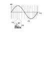
図5の波形図(1)は、商用周波数の交流波形の例を表す。商用周波数は、例えば、50Hz又は60Hzである。本実施の形態では、商用周波数を50Hzとして説明する。 A waveform diagram (1) in FIG. 5 represents an example of an AC waveform of a commercial frequency. A commercial frequency is, for example, 50 Hz or 60 Hz. In this embodiment, the commercial frequency is assumed to be 50 Hz.
図5のサンプリング切換タイミング(2)は、高速AD変換器1210がサンプリング周波数を切替えるタイミングを表す。商用周波数の交流波形の1周期毎に、高速AD変換器1210のサンプリング周波数が、180MHz又は200MHzのいずれかに切換えられる。このように高速AD変換器1210は、第1のサンプリング周波数(180MHz)でアナログ信号をデジタル信号に変換する処理と、第2のサンプリング周波数(200MHz)でアナログ信号をデジタル信号に変換する処理とを、交流波形の所定の周期毎に交互に切換える。
Sampling switching timing (2) in FIG. 5 represents the timing at which high-
図5のサンプリングデータ(3)は、交流波形の1周期毎に高速AD変換器1210から出力される180MHz又は200MHzの部分放電パルスのサンプリングデータを表す。180MHzと200MHzのサンプリングデータは、部分放電情報テーブル1305に記憶される最大値よりも大きいか否かを判定する大小判定が実施される。そして、大きい方の値で、部分放電情報テーブル1305のデータが更新される。
Sampling data (3) in FIG. 5 represents sampling data of a 180 MHz or 200 MHz partial discharge pulse output from the high-
部分放電情報テーブル1305に記録される全データは、通信部1400に渡された後、部分放電検出結果として外部ネットワーク50に出力される。そして、上位計測装置60が、外部ネットワーク50を介して部分放電情報テーブル1305の全データを受信して、総合的に部分放電の監視を実施する。
All the data recorded in the partial discharge information table 1305 are transferred to the
図6は、高速AD変換器1210における200MHzと180MHzサンプリング時の周波数帯域を示す説明図である。第1~第nのナイキスト境界は、サンプリング周波数の1/2の帯域間隔となる。即ち、ナイキストの境界は、例えば200MHzサンプリングの場合に100MHz毎に現れ、180MHzサンプリングの場合に90MHz毎に現れる。
FIG. 6 is an explanatory diagram showing frequency bands during sampling at 200 MHz and 180 MHz in the high-
図6の上段に示すように、部分放電パルスの周波数帯域は、50MHz~800MHzの範囲内で発生すると考えられる。このため、2種類のサンプリング周波数は、できるだけ広帯域でナイキスト境界が重複しないように設定される。ここで、サンプリング周波数の設定は、2種類のサンプリング周波数1/2(ナイキスト境界の周波数)の最小公倍数の値が、部分放電パルスの周波数帯域より大きい条件に設定する。
As shown in the upper part of FIG. 6, the frequency band of partial discharge pulses is considered to occur within the range of 50 MHz to 800 MHz. Therefore, the two kinds of sampling frequencies are set so that the Nyquist boundaries do not overlap in a wide band as much as possible. Here, the sampling frequency is set so that the value of the least common multiple of two kinds of
例えば部分放電パルスが200MHzであった場合、200MHzサンプリング条件では、部分放電パルスを検出できなくても、180MHzサンプリング条件では部分放電パルスを検出できる。逆に、部分放電パルスが180MHzであった場合、180MHzサンプリング条件では、部分放電パルスを検出できなくても、200MHzサンプリング条件では、部分放電パルスを検出できる。
以上により、サンプリング定理を満たさない高速AD変換器1210であっても、確実に部分放電パルスを観測することができる。
For example, if the partial discharge pulse is 200 MHz, even if the partial discharge pulse cannot be detected under the 200 MHz sampling condition, it can be detected under the 180 MHz sampling condition. Conversely, when the partial discharge pulse is 180 MHz, even if the partial discharge pulse cannot be detected under the 180 MHz sampling condition, it can be detected under the 200 MHz sampling condition.
As described above, even the high-
<交流波形の位相のカウント処理、及び部分放電の検出処理>
次に、部分放電のデータの処理方法のうちの、交流波形の位相のカウントと、部分放電の検出について、図7及び図8を参照して説明する。
図7は、交流波形の位相のカウントと、部分放電の検出処理の例を示すフローチャートである。
図8は、交流波形の1周期で大小判定部1306が部分放電を検出する様子を示す説明図である。
<Processing for counting phase of AC waveform and processing for detecting partial discharge>
Next, of the partial discharge data processing methods, counting of phases of AC waveforms and detection of partial discharge will be described with reference to FIGS. 7 and 8. FIG.
FIG. 7 is a flow chart showing an example of counting the phase of an AC waveform and detecting partial discharge.
FIG. 8 is an explanatory diagram showing how the
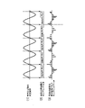
始めに、図7の最上部(即ち、開始時点)に示すように、位相ゼロ検出部1301が、50Hzの交流波形取得用の低速AD変換器1110から入力される交流波形サンプルデータに基づいて、交流波形の位相0°を検出する。
この時、図8に示すように、交流波形1310が左端のゼロクロス点となっている。
First, as shown at the top of FIG. 7 (that is, at the start point), the phase zero
At this time, as shown in FIG. 8, the
次に、位相ゼロ検出部1301が位相0°を検出したときに、位相ゼロ検出部1301から位相カウンタ1304へ、リセットパルス(初期化のパルス)を出力して、位相カウンタ1304を初期化する(S11)。この時、図8の左上に示すように、位相カウンタ1304の値が「0」になる。
Next, when phase zero
次に、位相カウンタ1304を参照し、部分放電情報テーブル1305より、検出最大値を取得する(S12)。ここで、位相カウンタ1304の位相が参照アドレスとして部分放電情報テーブル1305に送られる。そして、参照アドレスに対応する検出最大値(リードデータ)が部分放電情報テーブル1305から取得され、大小判定部1306に送られる。
Next, the
部分放電情報テーブル1305は、図8の右下に示すように、位相の3.75°毎の区間(96個の区間)の位相と、その位相の区間の交流波形10周期分の検出最大値(10周期分の部分放電の電荷量の最大値)とから構成されている。そして、大小判定部1306は、位相カウンタ1304の位相(0,3.75,7.5,・・・,356.25)の値を参照アドレスとして、部分放電情報テーブル1305から、その位相の区間の交流波形10周期分の検出最大値(リードデータ)を取得する。
The partial discharge information table 1305, as shown in the lower right of FIG. (the maximum value of the charge amount of partial discharge for 10 cycles). Then, the
次に、大小判定部1306は、高速AD変換器1210より取得した、部分放電のサンプルデータから部分放電の入力値(電荷量)を取得する(S13)。部分放電の入力値(電荷量)は、図8に示すように、高速AD変換器1210の180MHzのサンプリング間隔(5.55ns)、又は高速AD変換器1210の200MHzのサンプリング間隔(5ns)でサンプリングされた、部分放電パルス信号1320として表される。
Next, the
次に、大小判定部1306は、部分放電情報テーブル1305より取得した部分放電の検出最大値と、高速AD変換器1210より取得した部分放電の入力値(電荷量)を比較する(S14)。最大値(部分放電情報テーブル1305の検出最大値)<入力値の場合(S14のYes)、大小判定部1306は、部分放電情報テーブル1305の最大値(検出最大値)を入力値に更新して(S15)、ステップS16に進む。
Next, the
最大値(部分放電情報テーブル1305の検出最大値)≧入力値の場合(S14のNo)、部分放電情報テーブル1305の更新は行われない。そして、S14のNo、又はステップS15の処理の後、大小判定部1306は、サンプリング周波数の値が、180MHz又は200MHzのいずれであるかを判定する(S16)。
If the maximum value (maximum value detected in the partial discharge information table 1305)≧input value (No in S14), the partial discharge information table 1305 is not updated. Then, after No in S14 or after the processing in step S15, the
大小判定部1306により、サンプリング周波数の値が200MHzと判定された場合、高速ADデータ入力回数カウンタ1303は、高速AD変換器1210から41600回入力値を取得したか(位相3.75°を経過したか)を、経過時間に基づいて確認する(S17)。
When the
ここで、入力値の回数=(経過時間/サンプリング間隔5ns)であり、41600回の入力値となるのは約208μsである。このため、208μs経過する毎に、高速ADデータ入力回数カウンタ1303から信号を出力すればよい。 Here, the number of input values=(elapsed time/sampling interval 5 ns), and it takes about 208 μs to obtain 41,600 input values. Therefore, a signal may be output from the high-speed AD data input count counter 1303 every 208 μs.
そして、高速ADデータ入力回数カウンタ1303は、41600回入力値を取得した場合(S17のYes)、ステップS19に進む。一方、高速ADデータ入力回数カウンタ1303は、41600回入力値を取得していない場合(S17のNo)、ステップS12に戻って処理を続ける。 Then, when the high-speed AD data input frequency counter 1303 acquires the input value 41600 times (Yes in S17), the process proceeds to step S19. On the other hand, if the high-speed AD data input frequency counter 1303 has not acquired the input value 41600 times (No in S17), the process returns to step S12 to continue processing.
一方、ステップS16にて大小判定部1306により、サンプリング周波数の値が180MHzと判定された場合、高速ADデータ入力回数カウンタ1303は、高速AD変換器1210から37444回入力値を取得したか(位相3.75°を経過したか)を、経過時間に基づいて確認する(S18)。
On the other hand, if the
ここで、入力値の回数=(経過時間/サンプリング間隔5.55ns)であり、37444回の入力値となるのは約208μsである。このため、208μs経過する毎に、高速ADデータ入力回数カウンタ1303から信号を出力すればよい。 Here, the number of input values=(elapsed time/sampling interval 5.55 ns), and the input value of 37444 times is about 208 μs. Therefore, a signal may be output from the high-speed AD data input count counter 1303 every 208 μs.
そして、高速ADデータ入力回数カウンタ1303は、37444回入力値を取得した場合(S18のYes)、ステップS19に進む。一方、高速ADデータ入力回数カウンタ1303は、37444回入力値を取得していない場合(S18のNo)、ステップS12に戻って処理を続ける。 When the high-speed AD data input frequency counter 1303 acquires the input value 37444 times (Yes in S18), the process proceeds to step S19. On the other hand, if the high-speed AD data input count counter 1303 has not obtained an input value 37444 times (No in S18), the process returns to step S12 to continue processing.
このように、サンプリング周波数の値が、180MHzであれば37444回、サンプリング周波数の値が、200MHzであれば41600回、高速ADデータ入力回数カウンタ1303が入力値を取得するまで、ステップS12~S18の各ステップが繰り返される。これにより、図8に示す部分放電パルス信号1320の入力値(電荷量)のうちの最大値1330を、部分放電情報テーブル1305の検出最大値と比較することになる。そして、入力値の最大値1330の方が大きければ、部分放電情報テーブル1305の検出最大値が入力値の最大値1330に更新される。
In this way, steps S12 to S18 are performed until the high-speed AD data input count counter 1303 acquires the input value 37444 times if the sampling frequency value is 180 MHz, and 41600 times if the sampling frequency value is 200 MHz. Each step is repeated. As a result, the
ステップS17のYes、又はステップS18のYesの後、位相カウンタ1304を+3.75°進め(S19)、ステップS12に進む。この時、高速ADデータ入力回数カウンタ1303から、位相カウンタ1304へ、3.75°経過インクリメントの信号を出力する。
After Yes in step S17 or Yes in step S18, the
この時、図8においては、位相カウンタ1304が、次の位相の区間に移る。例えば位相3.75の区間から位相7.5の区間に移る。
At this time, in FIG. 8, the
そして、次の位相の区間について、部分放電の入力値の取得、及び、入力値と部分放電情報テーブル1305の検出最大値の比較が実行される。このようにして、交流波形の位相のカウントと、部分放電の検出が実行されることにより、交流波形の所定位相間隔の各区間について、部分放電の入力値(電荷量)が検出され、各区間の部分放電の電荷量の最大値が抽出される。 Then, for the section of the next phase, the partial discharge input value is acquired and the input value and the detected maximum value of the partial discharge information table 1305 are compared. By counting the phase of the AC waveform and detecting the partial discharge in this way, the input value (amount of charge) of the partial discharge is detected for each section of the AC waveform at predetermined phase intervals. is extracted.
さらに、交流波形1310の次の周期では、位相ゼロ検出部1301がサンプリングモードの切換えをサンプリング周波数切換器1220に指示する。そして、高速AD変換器1210のサンプリングモードが、前の交流波形1310の周期で設定されていたサンプリングモードとは異なるサンプリングモードに切換わる。例えば、前の周期で180MHzモードが設定されていれば、次の周期で200MHzのサンプリングモードが設定される。逆に、前の周期で200MHzのサンプリングモードが設定されていれば、次の周期で180MHzのサンプリングモードが設定される。その後、切換わったサンプリングモードにより、図7に示した処理が行われる。
Furthermore, in the next cycle of
<部分放電情報テーブルのクリアと、部分放電情報の通信部への送信処理>
次に、部分放電のデータの処理方法のうちの、部分放電情報テーブル1305のクリアと、部分放電情報の通信部1400への送信について、図4、図9及び図10を参照して説明する。
図9は、部分放電情報テーブル1305をクリアする処理と、部分放電情報の通信部1400への送信処理の例を示すフローチャートである。
図10は、部分放電情報テーブル1305がクリアされるタイミングと、部分放電情報が送信されるタイミングの例を示す説明図である。
<Clearing the partial discharge information table and transmitting the partial discharge information to the communication unit>
Next, clearing of the partial discharge information table 1305 and transmission of the partial discharge information to the
FIG. 9 is a flowchart showing an example of processing for clearing the partial discharge information table 1305 and processing for transmitting partial discharge information to the
FIG. 10 is an explanatory diagram showing examples of the timing at which the partial discharge information table 1305 is cleared and the timing at which the partial discharge information is transmitted.
始めに、交流波形の周期カウンタ1302が初期化される(S21)。この時、周期カウンタ1302は、図10に示すように、値「0」に初期化される。
First, the AC
次に、部分放電情報テーブル1305がクリアされる(S22)。この時、周期カウンタ1302から部分放電情報テーブル1305へ、テーブルクリアの信号が送られる。そして、図10に示すように、テーブルクリアの信号が入力された、部分放電情報テーブル1305がクリアされる。
Next, the partial discharge information table 1305 is cleared (S22). At this time, a table clear signal is sent from the
次に、位相ゼロ検出部1301は、交流波形の位相0°を検出したかを確認する(S23)。このステップS23は、図7のフローチャートの最上部(開始時点)に記載された、位相0°の検出と同じ処理を表す。位相ゼロ検出部1301が位相0°を検出した場合(S23のYes)、ステップS24に進み、位相0°を検出していない場合(S23のNo)、ステップS23の前に戻る。
Next, the phase zero
次に、ステップS23のYesの場合、周期カウンタ1302は、交流波形が10周期目であるかを確認する(S24)。交流波形が10周期目である場合(S24のYes)、ステップS25に進み、交流波形が10周期目ではない場合(S24のNo)、ステップS26に進む。
Next, in the case of Yes in step S23, the
周期カウンタ1302が、交流波形の10周期目と判定した場合(S24のYes)、部分放電情報テーブル1305から、部分放電情報テーブル1305の全データが通信部1400に送信される(S25)。その後、位相ゼロ検出部1301は、周期カウンタ1302を初期化する。
When the
この時、図10では、周期カウンタ1302の値が10周期目に当たる「9」である。その後、周期カウンタ1302が初期化されることにより、周期カウンタ1302の値が1周期目に当たる「0」に戻る。
At this time, in FIG. 10, the value of the
また、周期カウンタ1302を初期化し、部分放電情報テーブル1305をクリアする前に、通信部1400に送信した部分放電情報テーブル1305の全データが通信部1400から上位計測装置60へ送信される。そして、周期カウンタ1302を初期化する際に、部分放電情報テーブル1305のクリアも実行される。
All the data of the partial discharge information table 1305 transmitted to the
周期カウンタ1302が、交流波形の10周期目ではないと判定した場合(S24のNo)、位相ゼロ検出部1301からの交流周期インクリメントの信号が、周期カウンタ1302に入力されて、周期カウンタ1302がインクリメントされる(S26)。この時、図10に示すように、周期カウンタ1302の値が、0から1、1から2、2から3と、1つ増えて、交流波形の次の周期に移行する。
When the
このように、交流波形が10周期を経過するまで、ステップS23~S26の各ステップが繰り返される。これにより、交流波形の位相0°を起点として交流波形の周期が計測され、交流波形の10周期が経過する毎に、部分放電情報テーブル1305から全データが通信部1400に送信される。そして、周期カウンタ1302が初期化され、部分放電情報テーブル1305がクリアされた後、次の10周期における処理に移行する。
In this manner, steps S23 to S26 are repeated until the AC waveform has passed 10 cycles. As a result, the cycle of the AC waveform is measured starting from the phase of 0° of the AC waveform, and all the data is transmitted from the partial discharge information table 1305 to the
<上位計測装置におけるデータの推移の監視>
次に、上位計測装置60におけるデータの推移の監視について説明する。
上位計測装置60は、部分放電検出装置1000の通信部1400から受信した部分放電情報テーブル1305のデータを、過去に受信した部分放電情報テーブル1305を参照して、比較を行う。そして、通信部1400から受信した、現在の部分放電情報テーブル1305のデータが、参照した過去に受信した部分放電情報テーブル1305のデータと比較して、部分放電の検出最大値の増加が大きいと判定した場合には、電力ケーブル30に絶縁劣化の兆候があることを警告する。
<Monitoring data transition in host measuring device>
Next, monitoring of data transition in the
The
なお、上位計測装置60が参照する、過去に部分放電検出装置1000から受信した部分放電情報テーブル1305の受信時期は、ユーザーの設定により、1日前、1ヶ月前、1年前、等々、任意に選べるようにすることが好ましい。
また、部分放電の検出最大値の増加が大きいと判定する基準としては、例えば、検出最大値が2倍以上になる等、所定の基準を選定すればよい。
The reception timing of the partial discharge information table 1305 received from the partial
As a criterion for determining that the increase in the detected maximum value of partial discharge is large, a predetermined criterion such as doubling or more the detected maximum value may be selected.
<電力ケーブルの絶縁劣化の有無の判定方法>
次に、電力ケーブルの絶縁劣化の有無の判定方法について、説明する。
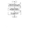
図11は、上位計測装置60が電力ケーブルの絶縁劣化の有無を判定する処理の例を示すフローチャートである。
<Method for Determining the Presence or Absence of Insulation Deterioration in Power Cables>
Next, a method for determining the presence or absence of insulation deterioration of a power cable will be described.
FIG. 11 is a flow chart showing an example of the process of determining whether or not the insulation of the power cable is deteriorated by the
始めに、図11の最上部(即ち、開始時点)に示すように、上位計測装置60が部分放電情報テーブル1305を受信する。即ち、通信部1400から送信された、部分放電情報テーブル1305の全データを、上位計測装置60で受信する。
First, the
次に、上位計測装置60は、過去に受信した部分放電情報テーブル1305を参照する(S31)。次に、上位計測装置60は、過去に受信したテーブルのデータと、現在の受信したテーブルのデータとを、交流波形の位相毎に比較する(S32)。
Next, the
そして、上位計測装置60は、過去と比較して部分放電として検出されたデータの最大値の増加が大きいか判定する(S33)。上位計測装置60は、過去と比較して部分放電として検出されたデータの最大値の増加が大きいと判定した場合(S33のYes)、「絶縁劣化の兆候有り」の警告を出力し(S34)、本処理を終了する。
Then, the
一方、上位計測装置60は、過去と比較して部分放電として検出されたデータの最大値の増加が大きくないと判定した場合(S33のNo)、「絶縁劣化の兆候無し」として、警告は行わず(S35)、本処理を終了する。
On the other hand, when the
このようにして、上位計測装置60において、絶縁劣化の兆候が有ると判定した場合には、警告を出力して、絶縁劣化の兆候を周知させることができる。
In this manner, when it is determined that there is a sign of insulation deterioration in the
以上説明した第1の実施の形態に係る部分放電検出装置1000では、部分放電パルスの周波数成分が、第1、第2、第3、第nナイキスト周波数帯域の境界になるのを防ぐため、高速AD変換器1210のサンプリング周波数を2種類(180MHz又は200MHz)としている。また、サンプリング周波数の切換は、商用周波数の周期毎のタイミングで実施される。
In the partial
このため、広帯域の部分放電パルスに対して、サンプリング定理を満たさない条件で高速AD変換器1210が部分放電パルスの観測を行い、商用周波数のタイミングで、2種類のサンプリング周波数を切換える。そして、高速AD変換器1210が高周波アナログ入力回路1200から入力されたアナログ信号をデジタル化する。大小判定部1306は、高周波アナログ入力回路1200から入力する部分放電のサンプルデータと、部分放電情報テーブル1305内のリードデータとを比較してデータの大小を判定し、大きい方のデータで部分放電情報テーブル1305を更新する。このため、部分放電情報テーブル1305により、部分放電検出のデジタル信号処理部1300が、サンプリング定理を満たさない条件で部分放電パルスの有無を検出できる。このように本実施の形態に係る部分放電検出装置1000では、あるサンプリング周波数でサンプリングされた部分放電の電流のアナログ信号のナイキスト境界に部分放電パルスの周波数帯域が重なっていても、別のサンプリング周波数でサンプリングされたアナログ信号のナイキスト境界とは異なる場所で部分放電パルスを検出することができる。
For this reason, the high-
また、上位計測装置60は、過去に受信した部分放電情報テーブル1305と、現在、受信した部分放電情報テーブル1305とを交流波形の位相毎に比較し、過去と比較して部分放電として検出されたデータの最大値の増加が大きいかを判定する。データの最大値の増加が大きければ、「絶縁劣化の兆候有り」の警告を行うことができる。
In addition, the
また、上述した実施の形態では、高速AD変換器1210のサンプリング周波数を180MHz又は200MHzとしたが、180MHz及び200MHz以外の異なるサンプリング周波数でサンプリングを行ってもよい。この場合であっても、2種類のサンプリング周波数の1/2の値の最小公倍数の値は、部分放電の周波数帯域より大きい値とすることが望ましい。
Also, in the above-described embodiment, the sampling frequency of the high-
[第2の実施の形態]
次に、本発明の第2の実施の形態に係る部分放電検出装置の構成例について、図12~図15を参照して説明する。
[Second embodiment]
Next, a configuration example of a partial discharge detection device according to a second embodiment of the invention will be described with reference to FIGS. 12 to 15. FIG.
図12は、第2の実施の形態に係る部分放電検出装置1000Aを用いて構成される部分放電検出システム1Aの概略構成例を示すブロック図である。
FIG. 12 is a block diagram showing a schematic configuration example of a partial discharge detection system 1A configured using the partial
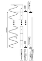
第2の実施の形態に係る部分放電検出システム1Aを構成する部分放電検出装置1000Aでは、電流測定器40に2つの高周波アナログ入力回路1200,1500が接続される。高周波アナログ入力回路1200,1500には、電流測定器40から同じアナログ信号(アナログ値)が入力される。
Two high-frequency
高周波アナログ入力回路1200からのアナログ信号が、第1高速AD変換器1230に入力される。第1高速AD変換器1230は、200MHz発振器1240から入力される200MHzのサンプリングクロックに基づいて、200MHzのサンプリング周波数で高周波アナログ入力回路1200から入力したアナログ信号をデジタル化する。そして、200MHzのサンプリング周波数でデジタル化された交流波形のデジタル信号が、部分放電検出のデジタル信号処理部1300Aに入力される。第1高速AD変換器1230がデジタル信号処理部1300Aに入力するデジタル信号を、「部分放電の第1サンプルデータ」とも呼ぶ。
An analog signal from high-frequency
また、高周波アナログ入力回路1500からのアナログ信号が、第2高速AD変換器1510に入力される。第2高速AD変換器1510は、180MHz発振器1520から入力される180MHzのサンプリングクロックに基づいて、180MHzのサンプリング周波数で、高周波アナログ入力回路1500から入力したアナログ信号をデジタル化する。そして、180MHzのサンプリング周波数でデジタル化された交流波形のデジタル信号が、部分放電検出のデジタル信号処理部1300Aに入力される。第2高速AD変換器1510がデジタル信号処理部1300Aに入力するデジタル信号を、「部分放電の第2サンプルデータ」とも呼ぶ。
Also, an analog signal from the high-frequency
部分放電検出のデジタル信号処理部1300Aは、低速AD変換器1110から入力される商用周波数の交流波形のデジタル信号、第1高速AD変換器1230及び第2高速AD変換器1510からそれぞれ入力される部分放電電流のデジタル信号に基づいて、部分放電検出のためのデジタル信号処理を行う。このため、本実施の形態に係る部分放電検出装置1000Aでは、第1の実施の形態に係る部分放電検出装置1000が備えていたサンプリング周波数切換器1220を不要となる。
The digital
<部分放電検出のデジタル信号処理部の構成例>
図13は、部分放電検出装置1000の部分放電検出のデジタル信号処理部1300Aの詳細な構成例を示すブロック図である。
<Configuration example of digital signal processing unit for partial discharge detection>
FIG. 13 is a block diagram showing a detailed configuration example of the partial discharge detection digital
部分放電検出のデジタル信号処理部1300Aは、第1の実施の形態に係る部分放電検出のデジタル信号処理部1300と同様の構成としているが、大小判定部1306Aに入力されるデータが異なる。具体的には、大小判定部1306Aに対して、第1高速AD変換器1230から部分放電の第1サンプルデータが入力され、第2高速AD変換器1510から部分放電の第2サンプルデータが入力される。
The partial discharge detection digital
そして、大小判定部1306Aは、部分放電の第1サンプルデータ及び第2サンプルデータを重ねた値と、部分放電情報テーブル1305から読み出した最大値のいずれが大きいか大小判定を実施する。部分放電の第1サンプルデータ及び第2サンプルデータを重ねた値が、部分放電情報テーブル1305から読み出した最大値より大きい場合に、大小判定部1306Aは、部分放電情報テーブル1305のデータを更新する。
Then, the
図14は、第1高速AD変換器1230及び第2高速AD変換器1510のサンプリングデータの例を示す説明図である。
FIG. 14 is an explanatory diagram showing an example of sampling data of the first high-
図14の波形図(1)は、商用周波数の交流波形の例を表す。商用周波数は、例えば、50Hz又は60Hzである。 A waveform diagram (1) in FIG. 14 represents an example of an AC waveform of a commercial frequency. A commercial frequency is, for example, 50 Hz or 60 Hz.
図14のサンプリングデータ(2)は、第1高速AD変換器1230が200MHzのサンプリング周波数でサンプリングした部分放電パルスのサンプリングデータを表す。このとき、第1高速AD変換器1230は、第1のサンプリング周波数(200MHz)でアナログ信号をデジタル信号に変換する処理を行う。
Sampling data (2) in FIG. 14 represents sampling data of a partial discharge pulse sampled by the first high-
図14のサンプリングデータ(3)は、第2高速AD変換器1510が180MHzのサンプリング周波数でサンプリングした部分放電パルスのサンプリングデータを表す。このとき、第2高速AD変換器1510は、第2のサンプリング周波数(180MHz)でアナログ信号をデジタル信号に変換する処理を行う。
Sampling data (3) in FIG. 14 represents sampling data of a partial discharge pulse sampled by the second high-
図14のサンプリングデータ(4)は、重ねられた200MHzのサンプリングデータと180MHzのサンプリングデータを表す。第1高速AD変換器1230及び第2高速AD変換器1510がそれぞれアナログ信号をデジタル信号に変換する処理は、交流波形の1周期を分割した同じ位相間隔毎に行われる。
Sampling data (4) in FIG. 14 represents superimposed 200 MHz sampling data and 180 MHz sampling data. The process of converting an analog signal into a digital signal by the first high-
このように200MHzのサンプリングデータと180MHzのサンプリングデータが重ねられることで、大小判定部1306Aは、商用周波数の交流波形の位相毎に、サンプリングデータの最大値を求めることが可能となる。
By superimposing the 200 MHz sampling data and the 180 MHz sampling data in this manner, the
図15は、交流波形の1周期で大小判定部1306Aが部分放電を検出する様子を示す説明図である。
上述したように、位相カウンタ1304の位相(0,3.75,7.5,・・・,356.25)毎に、200MHzのサンプリングデータと180MHzのサンプリングデータの値(入力値)が、部分放電情報テーブル1305から取得された交流波形10周期分の検出最大値と比較される。そして、最大値(部分放電情報テーブル1305の検出最大値)<入力値の場合、大小判定部1306Aは、部分放電情報テーブル1305の最大値(検出最大値)を、入力値に更新する。
FIG. 15 is an explanatory diagram showing how the
As described above, for each phase (0, 3.75, 7.5, . It is compared with the detected maximum value for 10 cycles of the AC waveform acquired from the discharge information table 1305 . Then, if maximum value (detected maximum value of partial discharge information table 1305)<input value,
交流波形の1周期における各位相で更新される最大値は、部分放電情報テーブル1305から読み出され、通信部1400を介して上位計測装置60に送られる。そして、上位計測装置60は、部分放電検出装置1000の通信部1400から受信した部分放電情報テーブル1305のデータと、過去に受信した部分放電情報テーブル1305を参照して得たデータとを比較する。上位計測装置60は、過去と比較して部分放電として検出されたデータの最大値の増加が大きいと判定した場合、「絶縁劣化の兆候有り」の警告を出力することができる。
The maximum value updated at each phase in one cycle of the AC waveform is read from the partial discharge information table 1305 and sent to the
以上説明した第2の実施の形態に係る部分放電検出装置1000Aでは、第1高速AD変換器1230及び第2高速AD変換器1510を備えたことで、交流波形の同じ位相間隔で、異なる2種類のサンプリング周波数でアナログ信号をデジタル化することが可能となる。そして、大小判定部1306Aは、2種類のサンプルデータを部分放電情報テーブル1305内のリードデータとを比較してデータの大小を判定する。これにより、部分放電検出のデジタル信号処理部1300が、部分放電パルスの有無を確実に確認できるようになる。
In the partial
[変形例]
上述した各実施の形態では、交流波形1310の特定の位相間隔を、96分割の位相3.75°の区間とし、さらに電荷量の最大値を抽出する交流波形1310の所定周期を10周期とした例で説明を行った。しかし、交流波形の特定の位相間隔の分割の数や、電荷量の最大値を抽出する交流波形の周期の数は、この例に限定されず、その他の数としてもよい。
そして、位相間隔の分割の数や、交流波形の周期の数をパラメータとして、任意に設定を変更できるよう制御可能なコンピュータプログラム等で構成してもよい。
[Modification]
In each of the above-described embodiments, the specific phase interval of the
Then, the number of divisions of the phase interval and the number of cycles of the AC waveform may be used as parameters, and a controllable computer program or the like may be used so that the settings can be arbitrarily changed.
また、電荷量の最大値を抽出する交流波形の周期の数は、例えば、部分放電を検出するナイキスト周波数領域の範囲に合わせて、第1ナイキスト領域のみの場合に1周期として、第1~第nナイキスト領域を確認する場合に(n×2)周期としてもよい。 Further, the number of cycles of the AC waveform for extracting the maximum value of the amount of charge is, for example, in accordance with the range of the Nyquist frequency region for detecting partial discharge, as one cycle in the case of only the first Nyquist region, the first to the first When confirming n Nyquist regions, it may be (n×2) cycles.
上述した各実施の形態では、図2や図8に示した部分放電パルス信号1320から、部分放電の電荷量を求める処理を、交流波形1310の特定の位相間隔の全区間(例えば、96分割の全区間)について行った。
これに対して、部分放電のデジタル信号処理部1300,1300Aは、交流波形の特定の位相間隔のうちの一部の区間について、部分放電の電荷量を求める処理を行うことも可能である。一部の区間について部分放電の電荷量を求めることにより、全区間について部分放電の電荷量を求めるよりも、データの量を予め減らすことが可能になる。
In each of the above-described embodiments, the process of obtaining the partial discharge charge amount from the partial
On the other hand, the partial discharge digital
ただし、部分放電のデジタル信号処理部1300,1300Aが、一部の区間について部分放電の電荷量を求めた場合には、部分放電の電荷量を求める処理を行わない区間において部分放電が発生したときに、発生した部分放電を検出することができない。したがって、実際の部分放電の発生頻度に対応して、部分放電の電荷量を求める処理を行う区間を選定することになる。
However, if the partial discharge digital
部分放電の発生頻度は、50Hzまたは60Hzの交流波形のゼロクロス(電流量の符号が変わるゼロ点、位相が0°,180°,360°の点)近傍が高く、部分放電はゼロクロスの前後に分布する。そこで、例えば、前述した96分割した96個の区間のうち、ゼロクロスの前後の部分放電の発生頻度が高い方の所定個数(例えば、50個や70個)の区間を選定して、選定した区間について部分放電の電荷量を求めればよい。 The frequency of occurrence of partial discharge is high in the vicinity of the zero crossing of the 50 Hz or 60 Hz AC waveform (the zero point where the sign of the current amount changes, the points where the phase is 0°, 180°, 360°), and the partial discharge is distributed before and after the zero crossing. do. Therefore, for example, among the 96 sections divided into 96 as described above, a predetermined number of sections (for example, 50 or 70) in which the frequency of occurrence of partial discharge before and after the zero cross is higher is selected, and the selected section can be obtained by calculating the charge amount of the partial discharge.
上述したように、部分放電のデジタル信号処理部1300,1300Aが、交流波形の特定の位相間隔のうちの一部の区間について、部分放電の電荷量を求める場合でも、交流波形のデジタル信号から交流波形の位相を求めて、求めた交流波形の位相を用いて特定の位相間隔に分割する。
As described above, even when the partial discharge digital
また、上述した各実施の形態と変形例では、交流波形の特定の位相間隔の全てまたは一部の区間について部分放電の電荷量を求め、所定周期数毎に電荷量の最大値を抽出するようにして、信号の量を低減していた。
部分放電のデジタル信号に対して、信号の量を低減する処理の方法は、上述した実施の形態と変形例の方法に限定されず、その他の方法を採用することもできる。その他の方法を採用する場合でも、交流波形のデジタル信号から交流波形の位相を求め、求めた交流波形の位相を用いて、部分放電のデジタル信号に対して、信号の量を低減する処理を行う。これにより、部分放電のデジタル信号を交流波形の位相と対応させることができるので、特定の位相であるゼロクロス近傍に発生しやすい部分放電をより確実に検出しつつ、部分放電のデジタル信号の量を低減することが可能になる。
Further, in each of the above-described embodiments and modifications, the charge amount of partial discharge is obtained for all or part of a specific phase interval of the AC waveform, and the maximum value of the charge amount is extracted for each predetermined number of cycles. to reduce the amount of signal.
The processing method for reducing the signal amount of the partial discharge digital signal is not limited to the methods of the above-described embodiments and modifications, and other methods can also be adopted. Even if other methods are adopted, the phase of the AC waveform is obtained from the digital signal of the AC waveform, and the obtained phase of the AC waveform is used to perform processing to reduce the signal amount of the digital signal of the partial discharge. . As a result, since the digital signal of partial discharge can correspond to the phase of the AC waveform, the amount of the digital signal of partial discharge can be detected while reliably detecting the partial discharge that tends to occur near the zero cross which is a specific phase. can be reduced.
なお、本発明は上述した実施の形態に限られるものではなく、特許請求の範囲に記載した本発明の要旨を逸脱しない限りその他種々の応用例、変形例を取り得ることは勿論である。
例えば、上述した実施の形態は本発明を分かりやすく説明するために装置及びシステムの構成を詳細かつ具体的に説明したものであり、必ずしも説明した全ての構成を備えるものに限定されない。また、ここで説明した実施の形態の構成の一部を他の実施の形態の構成に置き換えることは可能であり、さらにはある実施の形態の構成に他の実施の形態の構成を加えることも可能である。また、各実施の形態の構成の一部について、他の構成の追加、削除、置換をすることも可能である。
また、制御線や情報線は説明上必要と考えられるものを示しており、製品上必ずしも全ての制御線や情報線を示しているとは限らない。実際には殆ど全ての構成が相互に接続されていると考えてもよい。
It should be noted that the present invention is not limited to the above-described embodiment, and of course, various other applications and modifications can be made without departing from the gist of the present invention described in the claims.
For example, the above-described embodiments are detailed and specific descriptions of the configurations of devices and systems in order to explain the present invention in an easy-to-understand manner, and are not necessarily limited to those having all the configurations described. Further, it is possible to replace part of the configuration of the embodiment described here with the configuration of another embodiment, and furthermore, it is possible to add the configuration of another embodiment to the configuration of one embodiment. It is possible. Moreover, it is also possible to add, delete, or replace a part of the configuration of each embodiment with another configuration.
Further, the control lines and information lines indicate those considered necessary for explanation, and not all control lines and information lines are necessarily indicated on the product. In practice, it may be considered that almost all configurations are interconnected.
上述した実施の形態では、電力ケーブル30にロゴスキーコイル20を設置して電流信号を検出し、電圧位相情報を取得する構成例について説明した。電圧位相情報を計測する際は作業性、安全性を考慮する必要があることから、部分放電検出対象の電力ケーブル系統に変圧器を介して電圧変換した商用電源から交流電圧信号を取込み、電圧位相情報として取得しても実現できる。なお、商用電源の交流電圧信号とケーブル系統の交流電圧信号には変圧器を介することによる位相ずれが生じるが、この位相ずれを演算補正して対処することができる。
In the embodiment described above, a configuration example in which the
1…部分放電検出システム、40…電流測定器、60…上位計測装置、1000…部分放電検出装置、1100…低周波アナログ入力回路、1110…低速AD変換器、1200…高周波アナログ入力回路、1210…高速AD変換器、1220…サンプリング周波数切換器、1300…デジタル信号処理部、1301…位相ゼロ検出部、1302…周期カウンタ、1303…高速ADデータ入力回数カウンタ、1304…位相カウンタ、1305…部分放電情報テーブル、1306…大小判定部、1400…通信部
DESCRIPTION OF
Claims (6)
前記電力ケーブルに接続されたロゴスキーコイルから出力された商用周波数の交流波形のアナログ信号をデジタル信号に変換する第1の変換器と、
前記電力ケーブル同士を接続する中間接続箱が有する接地線に設けられた電流測定器が測定した前記部分放電の電流であって、第1のサンプリング周波数によって規定される複数のナイキスト領域、及び、前記第1のサンプリング周波数とは異なる第2のサンプリング周波数によって規定される複数のナイキスト領域の範囲内に含まれる部分放電の電流のアナログ信号をデジタル信号に変換する第2の変換器と、
前記第1の変換器で変換された前記電力ケーブルに流れる前記交流波形のデジタル信号から求めた前記交流波形の1周期を所定の位相間隔に分割して得られる区間の全区間について、前記第2の変換器で変換された前記部分放電の電流の前記デジタル信号から求めた電流値の最大値又は総和を算出し、前記最大値又は前記総和によって示される前記部分放電の電荷量の最大値の大きさに基づいて、前記部分放電の有無を検出する信号処理部と、を備え、
第1のサンプリング周波数及び第2のサンプリング周波数は、前記第1のサンプリング周波数の1/2の値と、前記第2のサンプリング周波数の1/2の値との最小公倍数の値が、前記部分放電の周波数帯域より大きくなる値に設定される
部分放電検出装置。 A partial discharge detection device for detecting a partial discharge in a power cable and grasping an insulation deterioration state of the power cable,
a first converter that converts an analog signal of a commercial frequency AC waveform output from the Rogowski coil connected to the power cable into a digital signal;
The current of the partial discharge measured by the current measuring device provided in the ground wire of the intermediate junction box connecting the power cables, wherein the current is a plurality of Nyquist regions defined by a first sampling frequency, and the a second converter for converting an analog signal of a partial discharge current contained within a plurality of Nyquist zones defined by a second sampling frequency different from the first sampling frequency into a digital signal;
For all the sections obtained by dividing one cycle of the AC waveform obtained from the digital signal of the AC waveform converted by the first converter and flowing in the power cable into predetermined phase intervals, the second calculating the maximum value or the sum of the current values obtained from the digital signal of the partial discharge current converted by the converter of the converter, and calculating the maximum value or the sum of the partial discharge charge amount indicated by the maximum value or the sum a signal processing unit that detects the presence or absence of the partial discharge based on the
The first sampling frequency and the second sampling frequency have a least common multiple value of 1/2 of the first sampling frequency and 1/2 of the second sampling frequency. A partial discharge detector set to a value greater than the frequency band of
前記テーブルに記録された前記データと、前記第2の変換器により変換された前記デジタル信号のデータとを同じ前記位相間隔毎に比較して大小判定を行い、前記テーブルに記録された前記データより大きい前記デジタル信号のデータにより前記テーブルに記録された前記データを更新する大小判定部と、を有する
請求項1に記載の部分放電検出装置。 The signal processing unit converts the data of the digital signal converted at the first sampling frequency by the second converter and the data of the digital signal converted at the second sampling frequency into the AC waveform. a table for recording every predetermined phase interval obtained by dividing one period;
The data recorded in the table and the data of the digital signal converted by the second converter are compared for each of the same phase intervals to determine the magnitude, and from the data recorded in the table 2. The partial discharge detection device according to claim 1, further comprising a magnitude determination unit that updates the data recorded in the table with the data of the digital signal that is greater.
請求項2に記載の部分放電検出装置。 The second converter performs a process of converting the analog signal into the digital signal at the first sampling frequency and a process of converting the analog signal into the digital signal at the second sampling frequency. 3. The partial discharge detection device according to claim 2, wherein the switching is alternately performed for each predetermined cycle of the AC waveform.
請求項2に記載の部分放電検出装置。 The second converter performs the same process of converting the analog signal into the digital signal at the first sampling frequency and converting the analog signal into the digital signal at the second sampling frequency. The partial discharge detection device according to claim 2, wherein the detection is performed at each phase interval.
請求項2~4のいずれか一項に記載の部分放電検出装置。 The partial discharge detection according to any one of claims 2 to 4, further comprising a communication unit connected to an external network and outputting the data recorded in the table to a host measuring device that monitors the partial discharge. Device.
前記電力ケーブルに接続されたロゴスキーコイルから出力された商用周波数の交流波形のアナログ信号を第1の変換器がデジタル信号に変換し、
前記電力ケーブル同士を接続する中間接続箱が有する接地線に設けられた電流測定器が測定した前記部分放電の電流であって、第1のサンプリング周波数によって規定される複数のナイキスト領域、及び、前記第1のサンプリング周波数とは異なる第2のサンプリング周波数によって規定される複数のナイキスト領域の範囲内に含まれる部分放電の電流のアナログ信号を第2の変換器がデジタル信号に変換し、
前記第1の変換器で変換された前記電力ケーブルに流れる前記交流波形のデジタル信号から求めた前記交流波形の1周期を所定の位相間隔に分割して得られる区間の全区間について、前記第2の変換器で変換された前記部分放電の電流の前記デジタル信号から求めた電流値の最大値又は総和を算出し、前記最大値又は前記総和によって示される前記部分放電の電荷量の最大値の大きさに基づいて、前記部分放電の有無を検出し、
第1のサンプリング周波数及び第2のサンプリング周波数は、前記第1のサンプリング周波数の1/2の値と、前記第2のサンプリング周波数の1/2の値との最小公倍数の値が、前記部分放電の周波数帯域より大きくなる値に設定される
部分放電検出方法。 A partial discharge detection method for detecting a partial discharge in a power cable and grasping an insulation deterioration state of the power cable,
A first converter converts an analog signal of a commercial frequency AC waveform output from a Rogowski coil connected to the power cable into a digital signal,
The current of the partial discharge measured by the current measuring device provided in the ground wire of the intermediate junction box connecting the power cables, wherein the current is a plurality of Nyquist regions defined by a first sampling frequency, and the a second converter converting analog signals of partial discharge currents contained within a plurality of Nyquist zones defined by a second sampling frequency different from the first sampling frequency into digital signals;
For all the sections obtained by dividing one cycle of the AC waveform obtained from the digital signal of the AC waveform converted by the first converter and flowing in the power cable into predetermined phase intervals, the second calculating the maximum value or the sum of the current values obtained from the digital signal of the partial discharge current converted by the converter of the converter, and calculating the maximum value or the sum of the partial discharge charge amount indicated by the maximum value or the sum detecting the presence or absence of the partial discharge based on the
The first sampling frequency and the second sampling frequency have a least common multiple value of 1/2 of the first sampling frequency and 1/2 of the second sampling frequency. A partial discharge detection method that is set to a value that is greater than the frequency band of
Priority Applications (5)
| Application Number | Priority Date | Filing Date | Title |
|---|---|---|---|
| JP2018232934A JP7130542B2 (en) | 2018-12-12 | 2018-12-12 | Partial discharge detection device and partial discharge detection method |
| PCT/JP2019/032828 WO2020121600A1 (en) | 2018-12-12 | 2019-08-22 | Partial discharge detection device and partial discharge detection method |
| US17/290,284 US11644498B2 (en) | 2018-12-12 | 2019-08-22 | Partial discharge detection apparatus and partial discharge detection method |
| SG11202104904RA SG11202104904RA (en) | 2018-12-12 | 2019-08-22 | Partial discharge detection apparatus and partial discharge detection method |
| EP19895244.2A EP3896467A4 (en) | 2018-12-12 | 2019-08-22 | Partial discharge detection device and partial discharge detection method |
Applications Claiming Priority (1)
| Application Number | Priority Date | Filing Date | Title |
|---|---|---|---|
| JP2018232934A JP7130542B2 (en) | 2018-12-12 | 2018-12-12 | Partial discharge detection device and partial discharge detection method |
Publications (2)
| Publication Number | Publication Date |
|---|---|
| JP2020094909A JP2020094909A (en) | 2020-06-18 |
| JP7130542B2 true JP7130542B2 (en) | 2022-09-05 |
Family
ID=71075532
Family Applications (1)
| Application Number | Title | Priority Date | Filing Date |
|---|---|---|---|
| JP2018232934A Active JP7130542B2 (en) | 2018-12-12 | 2018-12-12 | Partial discharge detection device and partial discharge detection method |
Country Status (5)
| Country | Link |
|---|---|
| US (1) | US11644498B2 (en) |
| EP (1) | EP3896467A4 (en) |
| JP (1) | JP7130542B2 (en) |
| SG (1) | SG11202104904RA (en) |
| WO (1) | WO2020121600A1 (en) |
Families Citing this family (3)
| Publication number | Priority date | Publication date | Assignee | Title |
|---|---|---|---|---|
| JP2022124610A (en) * | 2021-02-16 | 2022-08-26 | 株式会社東芝 | Partial discharge measurement system and partial discharge measurement method |
| CN114280432B (en) * | 2021-11-24 | 2023-10-13 | 浙江新图维电子科技有限公司 | Cable partial discharge monitoring equipment and method |
| JP2023172087A (en) * | 2022-05-23 | 2023-12-06 | 日東工業株式会社 | discharge detection system |
Family Cites Families (20)
| Publication number | Priority date | Publication date | Assignee | Title |
|---|---|---|---|---|
| JPH0580112A (en) * | 1991-09-24 | 1993-04-02 | Fujikura Ltd | Failure diagnostic device for power cable |
| JP3124359B2 (en) * | 1992-03-13 | 2001-01-15 | 古河電気工業株式会社 | Method and apparatus for measuring partial discharge of power cable |
| JP2670424B2 (en) * | 1994-02-14 | 1997-10-29 | 東京電力株式会社 | Partial discharge measurement system |
| JPH0996657A (en) * | 1995-09-29 | 1997-04-08 | Fujikura Ltd | Cable inspection equipment |
| JPH10170596A (en) | 1996-12-09 | 1998-06-26 | Hitachi Ltd | System for diagnosing insulated apparatus and method for detecting partial discharge |
| CA2508428A1 (en) * | 2005-05-20 | 2006-11-20 | Hydro-Quebec | Detection, locating and interpretation of partial discharge |
| US7112968B1 (en) * | 2005-11-30 | 2006-09-26 | Haneron Co., Ltd. | Method and apparatus for detecting a partial discharge in a high-voltage transmission and distribution system |
| KR101308812B1 (en) * | 2011-09-28 | 2013-09-13 | 한국전력공사 | Apparatus and method for noise elimination of partial discharge |
| AU2013389280B2 (en) * | 2013-05-10 | 2019-11-21 | Prysmian S.P.A. | Partial discharge signal processing method and apparatus employing neural network |
| KR101496442B1 (en) * | 2013-07-01 | 2015-02-27 | 한빛이디에스(주) | Partial discharge diagnosis device for the cable |
| JP2015040763A (en) * | 2013-08-22 | 2015-03-02 | 株式会社日立製作所 | Partial discharge measurement apparatus and method thereof |
| GB201315089D0 (en) * | 2013-08-23 | 2013-10-09 | Camlin Technologies Ltd | Diagnostic method for automatic discrimination of phase-to-ground partial discharge, phase-to-phase partial discharge and electromagnetic noise |
| JP6253775B2 (en) * | 2014-06-10 | 2017-12-27 | 株式会社日立製作所 | Partial discharge diagnosis system and partial discharge diagnosis method |
| JP6246751B2 (en) * | 2015-02-12 | 2017-12-13 | 株式会社日立製作所 | Insulation deterioration detection system, insulation deterioration detection method, and insulation deterioration detection sensor |
| KR101719741B1 (en) * | 2015-05-20 | 2017-03-24 | (주)스프링웨이브 | Apparatus and method for transmitting data to power cable diagnostic device |
| WO2017022032A1 (en) * | 2015-07-31 | 2017-02-09 | 株式会社日立製作所 | Partial discharge detection device and partial discharge detection method |
| KR101641515B1 (en) * | 2016-04-05 | 2016-07-22 | (주)서전기전 | The distribution panel including a diagnosis apparatus using HFCT |
| DE102017116613B3 (en) * | 2017-07-24 | 2018-08-09 | Maschinenfabrik Reinhausen Gmbh | Method and test device for measuring partial discharge pulses of a shielded cable |
| WO2019078602A1 (en) * | 2017-10-17 | 2019-04-25 | (주)에코투모로우코리아 | Device and method for processing partial discharge |
| WO2019182246A1 (en) * | 2018-03-18 | 2019-09-26 | Lg Electronics Inc. | Partial discharge detecting system |
-
2018
- 2018-12-12 JP JP2018232934A patent/JP7130542B2/en active Active
-
2019
- 2019-08-22 EP EP19895244.2A patent/EP3896467A4/en active Pending
- 2019-08-22 US US17/290,284 patent/US11644498B2/en active Active
- 2019-08-22 SG SG11202104904RA patent/SG11202104904RA/en unknown
- 2019-08-22 WO PCT/JP2019/032828 patent/WO2020121600A1/en unknown
Also Published As
| Publication number | Publication date |
|---|---|
| JP2020094909A (en) | 2020-06-18 |
| SG11202104904RA (en) | 2021-06-29 |
| EP3896467A4 (en) | 2022-10-05 |
| US20210373065A1 (en) | 2021-12-02 |
| EP3896467A1 (en) | 2021-10-20 |
| US11644498B2 (en) | 2023-05-09 |
| WO2020121600A1 (en) | 2020-06-18 |
Similar Documents
| Publication | Publication Date | Title |
|---|---|---|
| JP7130542B2 (en) | Partial discharge detection device and partial discharge detection method | |
| JP4955432B2 (en) | Waveform display device | |
| KR101472822B1 (en) | Method and apparatus for computing interpolation factors in sample rate conversion systems | |
| US9329659B2 (en) | Power monitoring system that determines frequency and phase relationships | |
| EP3588110B1 (en) | Partial discharge measurement system | |
| KR101423753B1 (en) | Instrument and method for measuring partial electrical discharges in an electrical system | |
| SE516135C2 (en) | Method and apparatus for digitizing a signal with large frequency bandwidth | |
| JP2001526768A (en) | Method and apparatus for signal waveform analysis | |
| WO2014141464A1 (en) | Merging unit for collecting electrical power system information | |
| WO2012079841A1 (en) | Combined measuring and detection system | |
| JPH09236621A (en) | Method and device for sampling | |
| EP3299828B1 (en) | Electrical fault detection | |
| KR20130029367A (en) | Instrument and method for detecting partial electrical discharges | |
| JP7003703B2 (en) | Partial discharge detection device using multi-sensor | |
| US20110298475A1 (en) | Method and device for monitoring a sheath voltage arrester of a cable system | |
| US20120330583A1 (en) | Instrument and method for detecting partial electrical discharges | |
| EP2074437A1 (en) | Method and device for monitoring a system | |
| KR20170052244A (en) | SDR Receiver for detecting doppler frequency in CW radar and method for detecting the same | |
| JP6886430B2 (en) | Partial discharge detection device and partial discharge detection method | |
| JP3082132B2 (en) | High voltage equipment insulation status monitor | |
| WO2018033436A1 (en) | Improvements in or relating to locating faults in power transmission conduits | |
| US10254330B2 (en) | Partial discharge detection bandwidth expansion through input signal aliasing | |
| CN108344925A (en) | A kind of power cable partial discharge monitoring device and method | |
| Khuzyashev et al. | Algorithms for locating current and voltage signal in a single phase-to-earth fault in distribution overhead networks | |
| US20120053875A1 (en) | Re-sampling acquired data to prevent coherent sampling artifacts |
Legal Events
| Date | Code | Title | Description |
|---|---|---|---|
| A621 | Written request for application examination |
Free format text: JAPANESE INTERMEDIATE CODE: A621 Effective date: 20201214 |
|
| A131 | Notification of reasons for refusal |
Free format text: JAPANESE INTERMEDIATE CODE: A131 Effective date: 20211102 |
|
| A521 | Request for written amendment filed |
Free format text: JAPANESE INTERMEDIATE CODE: A523 Effective date: 20211210 |
|
| A131 | Notification of reasons for refusal |
Free format text: JAPANESE INTERMEDIATE CODE: A131 Effective date: 20220322 |
|
| A521 | Request for written amendment filed |
Free format text: JAPANESE INTERMEDIATE CODE: A523 Effective date: 20220414 |
|
| TRDD | Decision of grant or rejection written | ||
| A01 | Written decision to grant a patent or to grant a registration (utility model) |
Free format text: JAPANESE INTERMEDIATE CODE: A01 Effective date: 20220816 |
|
| A61 | First payment of annual fees (during grant procedure) |
Free format text: JAPANESE INTERMEDIATE CODE: A61 Effective date: 20220824 |
|
| R150 | Certificate of patent or registration of utility model |
Ref document number: 7130542 Country of ref document: JP Free format text: JAPANESE INTERMEDIATE CODE: R150 |