JP7127066B2 - Detector for X-ray imaging - Google Patents
Detector for X-ray imaging Download PDFInfo
- Publication number
- JP7127066B2 JP7127066B2 JP2019563170A JP2019563170A JP7127066B2 JP 7127066 B2 JP7127066 B2 JP 7127066B2 JP 2019563170 A JP2019563170 A JP 2019563170A JP 2019563170 A JP2019563170 A JP 2019563170A JP 7127066 B2 JP7127066 B2 JP 7127066B2
- Authority
- JP
- Japan
- Prior art keywords
- detector
- edge
- semiconductor substrate
- charge
- region
- Prior art date
- Legal status (The legal status is an assumption and is not a legal conclusion. Google has not performed a legal analysis and makes no representation as to the accuracy of the status listed.)
- Active
Links
Images


Classifications
-
- G—PHYSICS
- G01—MEASURING; TESTING
- G01T—MEASUREMENT OF NUCLEAR OR X-RADIATION
- G01T1/00—Measuring X-radiation, gamma radiation, corpuscular radiation, or cosmic radiation
- G01T1/16—Measuring radiation intensity
- G01T1/24—Measuring radiation intensity with semiconductor detectors
- G01T1/241—Electrode arrangements, e.g. continuous or parallel strips or the like
-
- G—PHYSICS
- G01—MEASURING; TESTING
- G01T—MEASUREMENT OF NUCLEAR OR X-RADIATION
- G01T1/00—Measuring X-radiation, gamma radiation, corpuscular radiation, or cosmic radiation
-
- G—PHYSICS
- G01—MEASURING; TESTING
- G01T—MEASUREMENT OF NUCLEAR OR X-RADIATION
- G01T1/00—Measuring X-radiation, gamma radiation, corpuscular radiation, or cosmic radiation
- G01T1/16—Measuring radiation intensity
- G01T1/24—Measuring radiation intensity with semiconductor detectors
- G01T1/242—Stacked detectors, e.g. for depth information
-
- H—ELECTRICITY
- H10—SEMICONDUCTOR DEVICES; ELECTRIC SOLID-STATE DEVICES NOT OTHERWISE PROVIDED FOR
- H10B—ELECTRONIC MEMORY DEVICES
- H10B99/00—Subject matter not provided for in other groups of this subclass
Landscapes
- Physics & Mathematics (AREA)
- Health & Medical Sciences (AREA)
- Life Sciences & Earth Sciences (AREA)
- General Physics & Mathematics (AREA)
- High Energy & Nuclear Physics (AREA)
- Molecular Biology (AREA)
- Spectroscopy & Molecular Physics (AREA)
- Measurement Of Radiation (AREA)
- Solid State Image Pick-Up Elements (AREA)
- Transforming Light Signals Into Electric Signals (AREA)
- Light Receiving Elements (AREA)
Description
本発明は、概して、X線撮像のための検出器に関し、特に、光子計数X線撮像のための半導体ストリップ検出器、および検出器を製造する方法に関する。 The present invention relates generally to detectors for X-ray imaging, and more particularly to semiconductor strip detectors for photon-counting X-ray imaging, and methods of manufacturing detectors.
シリコン検出器などの半導体検出器は、X線撮像に広く使用されており、X線光子を検出し、相互作用する各光子によって放出された電荷キャリアを収集することにより、X線光子をデジタル信号またはデジタル画像に変換する。低エネルギーX線に関しては、検出器表面をX線に向けて、検出器面を複数の画素に分割することにより、半導体検出器を画素化するのが一般的である。各画素は、印加電界を通した画素内のX線相互作用によって生成された電荷を収集し、対応するフロントエンド電子回路に電荷を供給する。しかし、低い原子番号と低い密度のため、X線コンピュータ断層撮影などの高エネルギーX線による撮像では、例えばシリコン検出器の画素化構成は、0.5ミリメートル未満の基板厚さでは、全ての高エネルギーX線を捕捉することはできず、低い検出効率をもたらす。また、シリコンの原子番号が低いということは、検出器内のコンプトン散乱X線光子の一部が、光吸収光子よりも支配的であることを意味し、これは、散乱光子が検出器内の他の画素に信号を誘発することがあり、この信号はこれらの画素内ではノイズに等しいため、問題を生じさせる。 Semiconductor detectors, such as silicon detectors, are widely used in x-ray imaging to detect x-ray photons and convert them into a digital signal by collecting the charge carriers emitted by each interacting photon. Or convert to digital image. For low-energy x-rays, it is common to pixelate the semiconductor detector by facing the detector surface toward the x-rays and dividing the detector plane into a plurality of pixels. Each pixel collects charge generated by x-ray interaction within the pixel through an applied electric field and supplies the charge to corresponding front-end electronics. However, due to the low atomic number and low density, for imaging with high-energy X-rays, such as X-ray computed tomography, the pixelated configuration of e.g. Energetic X-rays cannot be captured, resulting in low detection efficiency. Also, the lower atomic number of silicon means that some of the Compton scattered X-ray photons in the detector predominate over the light-absorbed photons, which means that the scattered photons It can induce a signal in other pixels, which is tantamount to noise in those pixels and thus creates a problem.
シリコンの低吸収率の問題を解決する1つの方法は、シリコンの深度を、大幅に増加できるように、シリコン検出器のエッジを、入射X線に向けることにより、検出器のエッジオン構成を採用することである。X線検出器として、エッジオンジオメトリ(edge―on geometry)の結晶シリコンストリップ検出器を最初に言及したのは、R.ノヴォトニー(R. Nowotny)、“医学および構造解析におけるSiマイクロストリップ検出器の応用(Application of Si-microstrip-detectors in medicine and structural analysis)”、物理学研究における核計器および方法(Nuclear Instruments and Methods in Physics Research)226(1984)、34~39である。シリコンは、胸部撮影用など、低エネルギーで動作するが、主に、コンプトン散乱のより大きな部分およびこれに関連する問題のため、コンピュータ断層撮影などのより高エネルギー用ではないと結論づけている。 One method of solving the problem of low absorption of silicon employs an edge-on configuration of the detector by directing the edge of the silicon detector toward the incident x-rays so that the depth of the silicon can be greatly increased. That is. The first mention of edge-on geometry crystalline silicon strip detectors as X-ray detectors was made by R. R. Nowotny, "Application of Si-microstrip-detectors in medicine and structural analysis," Nuclear Instruments and Methods in Physics Research Physics Research) 226 (1984), 34-39. They conclude that silicon works at low energies, such as for chest imaging, but not for higher energies, such as computed tomography, mainly because of the larger fraction of Compton scattering and the problems associated with it.
半導体検出器のエッジオンジオメトリは、米国特許第4,937,453号、ロバート・ネルソン(Robert Nelson)“放射線撮像用X線検出器(X-ray detector for radiographic imaging)”、米国特許第5,434,417号、デイビッド・ナイグレン(David Nygren)“高解像度エネルギーに敏感なデジタルX線(High resolution energy-sensitive digital X-ray)”および米国特許第7,291,841号B2、ロバート・ネルソン(Robert Nelson)ら、“核医学における強化されたSPECT、PET、およびコンプトン散乱撮像のための装置およびシステム(Device and system for enhanced SPECT, PET, and Compton scatter imaging in nuclear medicine)”でも提案されている。米国特許第5,434,417号では、セグメント化されたシリコンストリップ検出器の概念が説明されているが、電荷収集電極が、どのようにフロントエンド電子回路に接続されているか、およびルーティングトレースの配置が示されていない。米国特許米国特許第7,291,841号B2では、エッジオン検出器は、本発明には関わらない、いわゆるコンプトン撮像に使用される。ショウイチ・ヨシダ(Shoichi Yoshida)、タカシ・オオスギ(Takashi Ohsugi)の論文“シリコンストリップ検出器のX線コンピュータ断層撮影への応用(Application of silicon strip detectors to X-ray computed tomography)”、物理学研究における核計器および方法(Nuclear Instruments and Methods in Physics Research)、A 541(2005)、412~420において、エッジオンコンセプトの実施が概説されている。この実施では、エッジオンシリコンストリップ検出器の間に配置された薄いタングステンプレートが、散乱X線の背景を減らし、低線量で画像コントラストを改善する。 The edge-on geometry of solid-state detectors is described in US Pat. No. 4,937,453, Robert Nelson "X-ray detector for radiographic imaging", US Pat. No. 5,434. , 417, David Nygren "High resolution energy-sensitive digital X-ray" and U.S. Patent No. 7,291,841 B2, Robert Nelson. Nelson et al., "Device and system for enhanced SPECT, PET, and Compton scatter imaging in nuclear medicine". U.S. Pat. No. 5,434,417 describes the concept of a segmented silicon strip detector, but how the charge collection electrodes are connected to the front end electronics and the routing traces. Placement not shown. In US Pat. No. 7,291,841 B2, edge-on detectors are used for so-called Compton imaging, which is not relevant to the present invention. Shoichi Yoshida, Takashi Ohsugi, "Application of silicon strip detectors to X-ray computed tomography", in physics research An implementation of the edge-on concept is reviewed in Nuclear Instruments and Methods in Physics Research, A 541 (2005), 412-420. In this implementation, a thin tungsten plate placed between edge-on silicon strip detectors reduces the background of scattered x-rays and improves image contrast at low doses.
エッジオンシリコンストリップ検出器の実装は、米国特許第8,183,535号B2、マッツ・ダニエルソン(Mats Danielsson)ら、“X線撮像用のシリコン検出器アセンブリ(Silicon detector assembly for x-ray imaging)”、チェン・シュウ(Cheng Xu)ら、“光子計数スペクトルCT用のセグメント化シリコンストリップ検出器のエネルギー分解能(Energy resolution of a segmented silicon strip detector for photon-counting spectral CT)”、物理学研究における核計器および方法(Nuclear Instruments and Methods in Physics Research)、715(2013)、11~17およびスジン・リウ(Xuejin Liu)ら、“マルチビン光子計数スペクトルコンピューター断層撮影検出器用のスペクトル応答モデルとその応用(Spectral response model for a multibin photon-counting spectral computed tomography detector and its applications)”、医用画像ジャーナル(Journal of Medical Imaging)2(3)(2015)033502に、さらに説明されている。そして、説明されるように、各ストリップは、深度セグメントにさらに分割され、X線コンピュータ断層撮影などの、X線撮像の高フラックス適用下でのフロントエンド電子回路の負荷を軽減する。各深度セグメントで検出された光子変換信号は、深度セグメントの対応する電荷収集電極と、フロントエンド電子回路のチャネルでの入力とを接続するルーティングトレースを介して、フロントエンド電子回路の個々の処理チャネルに伝達される。チェン・シュウ(Cheng Xu)らにより説明された、“光子計数スペクトルCT用のセグメント化シリコンストリップ検出器のエネルギー分解能(Energy resolution of a segmented silicon strip detector for photon-counting spectral CT)”、物理学研究における核計器および方法(Nuclear Instruments and Methods in Physics Research)、715(2013)、11~17には、2つの異なる金属層が、電荷収集電極用の1つの金属層と、ルーティングトレース用の他の層とを有するシリコン基板の電荷収集側に実装されている。マッツ・ダニエルソン(Mats Danielsson)の、スウェーデン特許出願第9801677-7号には、放射線療法の監視のために電荷収集電極間に延びるルーティングトレースを有するシリコン検出器が記載されている。E.ベラウ(E.BELAU)ら、“シリコンストリップ検出器での電荷収集(Charge collection in silicon strip detectors)”、物理学研究における核計器および方法(Nuclear Instruments and Methods in Physics Research)214(2-3)(1983)、253~260は、電荷収集電極と同じ層にルーティングトレースを有する粒子物理学に使用される望遠鏡検出器を説明している。マッツ・ダニエルソン(Mats Danielsson)ら、米国特許第8,183,535号B2の、コンプトン散乱が他のシリコン検出器に到達した結果としての散乱光子を部分的に止めるために、シリコン検出器のサブセットに取り付けられる“X線撮像用のシリコン検出器アセンブリ”では、薄くて重い金属シートが提案されている。 An implementation of an edge-on silicon strip detector is described in US Pat. No. 8,183,535 B2, Mats Danielsson et al., "Silicon detector assembly for x-ray imaging". , Cheng Xu et al., "Energy resolution of a segmented silicon strip detector for photon-counting spectral CT", Nuclear in Physics Research. Instruments and Methods in Physics Research, 715 (2013), 11-17 and Xuejin Liu et al., “Spectral response models and their applications for multi-bin photon-counting spectral computed tomography detectors (Spectral response model for a multibin photon-counting spectral computed tomography detector and its applications”, Journal of Medical Imaging 2(3) (2015) 033502. Each strip is then subdivided into depth segments, as described, to offload the front-end electronics under high flux applications of X-ray imaging, such as X-ray computed tomography. The photon-converted signal detected at each depth segment is transferred to the individual processing channels of the front-end electronics via routing traces connecting the depth segment's corresponding charge-collecting electrodes and the inputs at the channels of the front-end electronics. is transmitted to “Energy resolution of a segmented silicon strip detector for photon-counting spectral CT,” described by Cheng Xu et al., Physics Research Nuclear Instruments and Methods in Physics Research, 715 (2013), 11-17 describes two different metal layers, one for the charge collection electrodes and the other for the routing traces. is mounted on the charge collection side of a silicon substrate having a layer. Mats Danielsson, Swedish Patent Application No. 9801677-7, describes a silicon detector with routing traces extending between charge collection electrodes for radiation therapy monitoring. E. E. BELAU et al., “Charge collection in silicon strip detectors,” Nuclear Instruments and Methods in Physics Research 214(2-3). (1983), 253-260 describe a telescopic detector used in particle physics with routing traces in the same layer as the charge collection electrodes. In order to partially stop scattered photons as a result of Compton scattering reaching other silicon detectors, Mats Danielsson et al., U.S. Pat. No. 8,183,535 B2. Thin and heavy metal sheets have been proposed in "Silicon Detector Assemblies for X-Ray Imaging" mounted on subsets.
キャパシタンスは、検出器に関する最も重要なパラメータの1つであり、フロントエンド電子回路の電子ノイズのレベルに直接関連する。ノイズレベルは、任意の撮像検出器が満足のいく品質で画像を取得するために、可能な限り低くする必要がある。検出された光子が特定の時間間隔にわたって統合されるエネルギー統合検出器の場合、電子ノイズが読み出し信号に吸収され、結果として画質の低下をもたらす。光子計数検出器の場合、ノイズによって誘発される偽の計数を拒絶するには、最低エネルギー閾値を、ノイズフロアのレベルよりも高く設定する必要がある。したがって、新しい検出器を設計する場合、フロントエンド電子回路への入力容量を下げることは、重要なタスクである。 Capacitance is one of the most important parameters for detectors and is directly related to the level of electronic noise in the front-end electronics. The noise level should be as low as possible for any imaging detector to acquire images with satisfactory quality. For energy integrating detectors in which the detected photons are integrated over a specific time interval, electronic noise is absorbed in the readout signal, resulting in image quality degradation. For photon-counting detectors, the lowest energy threshold should be set above the level of the noise floor to reject noise-induced false counts. Reducing the input capacitance to the front-end electronics is therefore an important task when designing new detectors.
シリコン検出器などの半導体検出器の場合、片面シリコンストリップ検出器を特定の例とすると、次の2つの寄与が、主なキャパシタンス源であり、それは、電荷収集電極とシリコン基板の裏面との間のキャパシタンスである裏面キャパシタンス、および隣接する電荷収集電極間のキャパシタンスであるストリップ間キャパシタンスである。電荷収集電極とフロントエンド電子回路の入力とを接続するルーティングトレースを有する検出器の場合、トレースキャパシタンスも重要な役割を果たし、トレースキャパシタンスには、隣接するルーティングトレース間のキャパシタンスと、ルーティングトレースと電荷収集電極との間のキャパシタンスと、が含まれまる。X線に敏感な領域の範囲外では、シリコン基板は注入層の大きな領域によって覆われていることがあり、その上に延びるルーティングトレースが存在する場合、これもキャパシタンスに寄与する。 In the case of semiconductor detectors such as silicon detectors, taking a single-sided silicon strip detector as a particular example, the following two contributions are the main sources of capacitance: between the charge collection electrode and the backside of the silicon substrate. and the inter-strip capacitance, which is the capacitance between adjacent charge collection electrodes. For detectors with routing traces connecting the charge collection electrodes to the inputs of the front-end electronics, trace capacitance also plays an important role, including the capacitance between adjacent routing traces and the capacitance between routing traces and charge and the capacitance between the collecting electrodes. Outside the x-ray sensitive area, the silicon substrate may be covered by a large area of implanted layer, which also contributes to the capacitance if there are routing traces extending over it.
特に高エネルギーX線による撮像のための医療撮像用のエッジオンシリコン検出器に、大きな関心が寄せられている。しかし、深度セグメントの数が1よりも大きい場合、フロントエンド電子回路へのルーティングに関連して、問題が発生する。チェン・シュウ(Cheng Xu)ら、“光子計数スペクトルCT用のセグメント化シリコンストリップ検出器のエネルギー分解能(Energy resolution of a segmented silicon strip detector for photon-counting spectral CT)”、物理学研究における核計器および方法(Nuclear Instruments and Methods in Physics Research)、715(2013)、11~17に、2つの金属層を有する設計が説明されているが、ルーティングトレースは、電荷収集金属電極のものとは異なる金属層上で動作しており、より高いキャパシタンスと実装の複雑さを示している。そして、2つの金属層間の絶縁体材料によって、より多くのデッドスペースが追加され、これは、幾何学的効率の損失をもたらしている。また、米国特許第8,183,535号B2、マッツ・ダニエルソン(Mats Danielsson)ら、“X線撮像用のシリコン検出器アセンブリ(Silicon detector assembly for x-ray imaging)”では、フロントエンド電極を、センサの領域またはセンサの上部に展開することが提案されているが、そうした場合、フロントエンド電子回路が、放射線にさらされ、フロントエンド電子回路も、スペースを取り、非常に高密度の梱包を不可能にする。したがって、実装の複雑さを低下させ、フロントエンド電子回路への最適なキャパシタンスで、ルーティングトレースをフロントエンド電子回路に導通する方法を提供することが望ましい。 There is great interest in edge-on-silicon detectors for medical imaging, especially for imaging with high-energy X-rays. However, when the number of depth segments is greater than one, problems arise with regard to routing to the front-end electronics. Cheng Xu, et al., "Energy resolution of a segmented silicon strip detector for photon-counting spectral CT," Nuclear instrumentation and A design with two metal layers is described in Nuclear Instruments and Methods in Physics Research, 715 (2013), 11-17, but the routing traces are in a different metal layer than that of the charge collection metal electrode. , showing higher capacitance and implementation complexity. And the insulator material between the two metal layers adds more dead space, which leads to a loss of geometric efficiency. Also, in U.S. Pat. No. 8,183,535 B2, Mats Danielsson et al., "Silicon detector assembly for x-ray imaging," a front-end electrode is , has been proposed to be deployed in the area of the sensor or on top of the sensor, but in doing so the front-end electronics would be exposed to radiation, and the front-end electronics would also take up space and require very dense packaging. make impossible. Therefore, it is desirable to provide a method of conducting routing traces to front-end electronics with reduced implementation complexity and optimum capacitance to the front-end electronics.
提案技術は、電荷収集電極をフロントエンド電子回路の入力に接続するルーティングトレースを有する検出器に関連する、キャパシタンス関連の問題のいくつかを少なくとも軽減する、エッジオン半導体検出器を提供することを目的とする。 The proposed technique aims to provide an edge-on semiconductor detector that alleviates at least some of the capacitance-related problems associated with detectors having routing traces connecting charge collection electrodes to inputs of front-end electronics. do.
提案技術の特定の目的は、改善されたキャパシタンス特性を有する光子計数エッジオン半導体検出器を提供することである。特に、低いキャパシタンスを有する光子計数エッジオン半導体検出器を提供することである。 A particular object of the proposed technique is to provide a photon-counting edge-on semiconductor detector with improved capacitance properties. In particular, it is to provide a photon-counting edge-on semiconductor detector with low capacitance.
もう1つの目的は、改善されたキャパシタンス特性、特に低いキャパシタンス特性を有する光子計数エッジオン半導体検出器を製造する方法を提供することである。 Another object is to provide a method of manufacturing a photon-counting edge-on semiconductor detector with improved capacitance properties, particularly low capacitance properties.
提案技術の第1の態様によれば、エッジオン光子計数検出器が提供される。検出器は、X線源に対向するように構成された第1の端部と、入射X線の方向において、第1の端部の反対側にある第2の端部と、を備えた半導体基板を備える。半導体基板は、N≧2とするN個の深度セグメントを有する少なくとも1つのストリップを備える。深度セグメントのそれぞれが、電荷収集金属電極を備える。半導体基板は、また、ドープ領域と絶縁領域とを備えた電荷収集側を備える。電荷収集金属電極のそれぞれは、対応するドープ領域の上に配置され、絶縁領域上に配置された、それぞれのルーティングトレースに接続される。それぞれのルーティングトレースは、電荷収集金属電極から、第2の端部に配置されたフロントエンド電子回路に接続可能な読み出しパッドEへと信号を伝達するように構成されている。 According to a first aspect of the proposed technique, an edge-on photon counting detector is provided. The detector is a semiconductor with a first end configured to face the X-ray source and a second end opposite the first end in the direction of incident X-rays. A substrate is provided. The semiconductor substrate comprises at least one strip having N depth segments, N≧2. Each depth segment comprises a charge collecting metal electrode. The semiconductor substrate also has a charge collecting side with a doped region and an insulating region. Each of the charge collecting metal electrodes is disposed over the corresponding doped region and connected to a respective routing trace disposed over the insulating region. Each routing trace is configured to carry a signal from the charge collection metal electrode to a readout pad E connectable to front end electronics located at the second end.
提案技術の第2の態様によれば、エッジオン検出器のための電荷収集面を製造するための方法が提供される。 According to a second aspect of the proposed technique, a method is provided for manufacturing a charge collection surface for an edge-on detector.
方法は、半導体基板を供給するステップを含み、半導体基板は、X線源に対向するように構成された第1の端部と、第1の端部の反対側にある第2の端部と、を有する。方法は、また、電荷収集面と称される、半導体基板の表面に、ドープ領域を設けるステップを含み、ドープ領域は、第1の種類のドーピングを有する。方法は、また、ドープ領域が設けられていない第2の表面の領域に、絶縁層を設けるステップを含む。方法は、また、半導体基板の第2の端部に、読み出しパッドを配置するステップを含む。方法は、さらに、ドープ領域と、絶縁層とを備える電荷収集面の上に、単一金属層を成膜するステップを含む。方法は、さらに、単一金属層をパターニングして、i)ドープ領域の上に、電荷収集金属電極を形成し、ii)絶縁層の上に、電荷収集金属電極を読み出しパッドと接続するルーティングトレースを形成するステップを含む。 The method includes providing a semiconductor substrate, the semiconductor substrate having a first end configured to face an x-ray source and a second end opposite the first end. , has The method also includes providing a doped region in the surface of the semiconductor substrate, referred to as a charge collecting surface, the doped region having a first type of doping. The method also includes providing an insulating layer in regions of the second surface not provided with doped regions. The method also includes disposing a read pad at the second end of the semiconductor substrate. The method further includes depositing a single metal layer over the charge collection surface comprising the doped regions and the insulating layer. The method further includes patterning the single metal layer to i) form a charge collecting metal electrode over the doped region and ii) a routing trace connecting the charge collecting metal electrode with the readout pad over the insulating layer. forming a.
提案技術の実施形態は、優れたキャパシタンス特性を有するエッジオン検出器を提供する。このような検出器は、フロントエンド電子回路でノイズレベルが減少することを確保し、これは、取得画像の質を高める。さらなる利点は、後のセクションを読むことにより、明らかとなる。 Embodiments of the proposed technique provide edge-on detectors with excellent capacitance properties. Such detectors ensure a reduced noise level in the front-end electronics, which enhances the quality of acquired images. Further advantages will become apparent from reading the later sections.
本発明は、改善されたキャパシタンス特性を有するエッジオン半導体ストリップ検出器を、提供することを目的とする。提供されるストリップ検出器は、40keV~250keVのエネルギー範囲内でのX線撮像における使用に適している。この目的を達成するために、金属層を、検出器の電荷収集側に実装して、電荷収集電極と同じ金属層に延びる導電ルーティングトレースを得るようにしてもよい。さらに、ストリップ検出器に関連するキャパシタンスを減少させるための方法および方策が提供される。 SUMMARY OF THE INVENTION It is an object of the present invention to provide an edge-on semiconductor strip detector with improved capacitance characteristics. The provided strip detector is suitable for use in X-ray imaging within the energy range of 40 keV to 250 keV. To this end, a metal layer may be implemented on the charge collection side of the detector with conductive routing traces extending to the same metal layer as the charge collection electrodes. Additionally, methods and strategies are provided for reducing the capacitance associated with strip detectors.
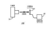
提案技術の様々な実施形態を説明する前に、エッジオン半導体ストリップ検出器が用いられる技術の概要から始めるのが、有用であろう。このために、図11を参照する。この非限定の例において、X線撮像システム100は、基本的には、X線源10と、X線検出システム20と、関連する画像処理デバイス30と、を備える。一般に、X線検出システム20は、任意のX線光学素子により焦点を合わされ、物体または被験者あるいはその一部を通過した可能性がある、X線源10からの放射を記録するように構成されている。X線検出システム20は、適切なアナログ処理および読み出し電子部品(X線検出システム20に一体化してもよい)を介して、画像処理デバイス30に接続可能であり、画像処理デバイス30による画像処理および/または画像再構築を可能にする。
Before describing various embodiments of the proposed technique, it may be helpful to begin with an overview of the technique in which edge-on semiconductor strip detectors are used. For this purpose, reference is made to FIG. In this non-limiting example, the
図12に示すように、X線撮像システム100の別の例は、X線を放射するX線源10と、物体を通過した後のX線を検出するX線検出システム20と、検出器からの生電気信号を処理し、デジタル化するアナログ処理回路25と、補正を適用する、測定データを一時保存する、またはフィルタリングするなどのさらなる処理動作を、測定データに対して実行することが可能なデジタル処理回路40と、処理データを保存し、さらなる後処理および/または画像再構築を行うことが可能なコンピュータ50と、を備える。
As shown in FIG. 12, another example of an
全体的な検出器を、X線検出システム20とみなしてもよく、または、X線検出システム20を、関連するアナログ処理回路25と組み合わせてもよい。
The overall detector may be considered an
デジタル処理回路40および/またはコンピュータ50を含むデジタル部は、X線検出器からの画像データに基づき画像再構築を行う、デジタル画像処理システム30とみなしてもよい。画像処理システム30は、よって、コンピュータ50、または代替案としてデジタル処理回路40とコンピュータ50との複合システムとして、あるいは場合によっては、デジタル処理回路をさらに画像処理および/または再構築に専用のものとする場合は、デジタル処理回路40自体として考えてもよい。
The digital portion, including
一般的に用いられるX線撮像システムの例は、コンピュータ断層撮影(CT)システムであり、このシステムは、X線のファンまたはコーンビームを生成するX線源と、患者または物体を透過したX線の部分を記録するための対向するX線検出システムと、を含んでもよい。X線源および検出システムは、通常、撮像される物体の周りを回転するガントリーに搭載される。 An example of a commonly used X-ray imaging system is a computed tomography (CT) system, which includes an X-ray source that produces a fan or cone beam of X-rays and an X-ray beam that passes through a patient or object. and a facing X-ray detection system for recording portions of the . The x-ray source and detection system are typically mounted on a gantry that rotates around the object to be imaged.
このため、図12に示されるX線源10と、X線検出システム20とは、CTシステムの一部として配置してもよく、例えば、CTガントリーに搭載可能であってもよい。
Thus, the
X線撮像検出器に関する課題は、検出されたX線から最大の情報を抽出し、物体または被験者が密度、組成および構造に関して描写される、物体または被験者の画像に対する入力を供給することである。検出器として、フィルム画像を用いることが、なお一般的であるが、今日の検出器は、最も一般的には、デジタル画像を提供する。 The challenge with X-ray imaging detectors is to extract the maximum information from the detected X-rays and provide input for an image of an object or subject in which the object or subject is delineated in terms of density, composition and structure. Although it is still common to use film images as detectors, today's detectors most commonly provide digital images.
提案技術は、一部は、半導体エッジオン検出器の特定の設計に関する。半導体エッジオン検出器は、任意の適切な半導体材料を備えてもよい。提案技術の特定の実施形態は、シリコンの検出器基板に関する。しかし、他の材料も可能である。光子計数X線検出器のための将来有望な材料は、テルル化カドミウム(CdTe)、テルル化亜鉛カドミウム(CZT)およびシリコン(Si)である。CdTeおよびCZTは、臨床CTで用いられる高エネルギーX線の高い吸収効率のため、いくつかの光子計数スペクトルCTプロジェクトで採用されている。しかし、これらのプロジェクトは、CdTe/CZTのいくつかの欠点のため進行が遅い。CdTe/CZTは、低い電荷キャリア移動度を有し、これは、臨床診療で見られるものよりも、10分の1のフラックスレートで、いくつかのパルスパイルアップを引き起こす。この問題を軽減する1つのやり方は、画素サイズを減少させることであるが、電荷共有およびKエスケープの結果として、スペクトル歪みの増加をもたらす。また、CdTe/CZTは、電荷トラッピングを受け、これは、光子フラックスが特定レベルを上回ると、出力計数率の急激な降下を起こす極性化をもたらす。 The proposed technique relates, in part, to a specific design of a semiconductor edge-on detector. A semiconductor edge-on detector may comprise any suitable semiconductor material. Particular embodiments of the proposed technology relate to silicon detector substrates. However, other materials are also possible. Promising materials for photon counting X-ray detectors are cadmium telluride (CdTe), cadmium zinc telluride (CZT) and silicon (Si). CdTe and CZT have been employed in some photon-counting spectral CT projects due to their high absorption efficiency of the high-energy X-rays used in clinical CT. However, these projects have been slow due to some drawbacks of CdTe/CZT. CdTe/CZT has low charge carrier mobility, which causes some pulse pile-up at flux rates ten times lower than those seen in clinical practice. One way to alleviate this problem is to reduce the pixel size, but this results in increased spectral distortion as a result of charge sharing and K escape. CdTe/CZT also suffers from charge trapping, which leads to polarization causing a sharp drop in output count rate when the photon flux exceeds a certain level.
対照的に、シリコンは、より高い電荷キャリア移動度を有し、極性化の問題もない。成熟した製造過程と、比較的低いコストも、その利点である。しかし、シリコンは、CdTe/CZTが持たない制限も有する。これに応じて、シリコンセンサは、その低い阻止能を補償するために、非常に厚くしなければならない。典型的には、シリコンセンサは、入射する光子のほとんどを吸収するために、数センチメートルの厚さを必要とするのに対し、CdTe/CZTは、数ミリメートルのみを必要とする。他方で、シリコンの長い減衰経路は、検出器を、以下に述べるように、異なる深度セグメントに分割することを可能にする。これは、一方で、シリコンベースの光子計数検出器が、CT内の高いフラックスを正しく処理することを可能にする。 In contrast, silicon has higher charge carrier mobility and no polarization problems. A mature manufacturing process and relatively low cost are also advantages. However, silicon also has limitations that CdTe/CZT does not. Correspondingly, silicon sensors must be made very thick to compensate for their low stopping power. Typically, silicon sensors require a thickness of several centimeters to absorb most of the incident photons, whereas CdTe/CZT only require a few millimeters. On the other hand, the long attenuation path of silicon allows splitting the detector into different depth segments, as described below. This, in turn, allows silicon-based photon-counting detectors to correctly handle high fluxes in CT.
図13は、半導体検出モジュールの例を示す模式図を提供する。これは、センサ部21を、検出素子または画素22に分割した半導体検出モジュールの例であり、各検出素子(または画素)は、通常、主要な構成要素として、電荷収集電極を有するダイオードに基づく。X線は、半導体検出器のエッジから入る。図16に見られるように、検出素子は、検出器の表面に沿って、個別のストリップ状に配置してもよい。
FIG. 13 provides a schematic diagram illustrating an example of a semiconductor detection module. This is an example of a semiconductor sensing module that divides the
図14は、別の例示的な実施形態に係る半導体検出モジュールの例を示す模式図である。この例では、半導体センサ部21は、深度方向で、いわゆる深度セグメント22に分割されており、再び、X線はエッジから入るものとしている。検出素子のそれぞれは、電荷収集電極と、電荷収集電極からの信号を、フロントエンド電子回路に伝達するように構成されている、対応するルーティングトレースと、を備えることに留意すべきである。通常、このような検出素子は、検出器の個別のX線検知サブ素子である。一般に、光子相互作用は、検出素子内で起こり、よって、生成される電荷は、検出素子の対応電極によって収集される。各検出素子は、典型的には、フレームの連続として、入射X線フラックスを測定する。フレームは、フレーム時間と呼ばれる特定の時間間隔内で測定されたデータである。
FIG. 14 is a schematic diagram illustrating an example semiconductor detection module according to another exemplary embodiment. In this example, the
図15は、別の例示的な実施形態に係る半導体検出モジュールの模式図である。ルーティングトレースCは、検出器の電荷収集電極を、フロントエンド電子回路Vの入力に接続する。読み出しパッドは、図15では開示されず、代わりに、ルーティングトレースを、検出器に取り付けられたフロントエンド電子回路または回路に、どのようにして接続するかを示している。読み出しパッドは、この図では、フロントエンド電子回路の下に配置されている。 FIG. 15 is a schematic diagram of a semiconductor detection module according to another exemplary embodiment. Routing traces C connect the charge collection electrodes of the detector to the inputs of front-end electronics V. FIG. The readout pads are not disclosed in FIG. 15, instead showing how the routing traces are connected to the front end electronics or circuitry attached to the detector. The read pad is located below the front end electronics in this figure.
検出器トポロジーに応じて、検出素子は、特に検出器がフラットパネル検出器である場合、画素に対応してもよい。深度セグメント化された検出器は、各ストリップが複数の深度セグメントを有する、複数の検出ストリップを有するものとみなしてもよい。このような深度セグメント化された検出器に関して、各深度セグメントは、特に深度セグメントのそれぞれが、それ自体の個別の電荷収集電極と関連する場合、個別の検出素子とみなしてもよい。 Depending on the detector topology, the detector elements may correspond to pixels, particularly if the detector is a flat panel detector. A depth segmented detector may be viewed as having multiple detection strips, each strip having multiple depth segments. With respect to such depth-segmented detectors, each depth segment may be considered a separate detector element, particularly if each depth segment is associated with its own separate charge collection electrode.
深度セグメント化された検出器の検出ストリップは、通常、一般的なフラットパネル検出器の画素に対応する。しかし、深度セグメント化された検出器を、個別の深度/検出素子に対応する各画素(時にはボクセルと称される)である、3次元画素アレイとみなすことも可能である。 The detector strips of a depth-segmented detector typically correspond to the pixels of a common flat panel detector. However, it is also possible to consider a depth-segmented detector as a three-dimensional pixel array, with each pixel (sometimes referred to as a voxel) corresponding to a separate depth/detector element.
エッジオン検出器を用いることが可能な包括的システムを説明したが、以下、改善されたキャパシタンス特性を提供する特定のエッジオン検出器を説明する。 Having described a generic system that can use edge-on detectors, a specific edge-on detector that provides improved capacitance characteristics will now be described.
提案技術は、半導体基板102を備えるエッジオン光子計数検出器を提供し、半導体基板102は、
・X線源に対向するように構成された第1の端部11と、入射X線の方向において、第1の端部11の反対側にある第2の端部12と、
・N≧2とするN個の深度セグメントを有し、深度セグメントのそれぞれが、電荷収集金属電極104を備える、少なくとも1つのストリップと、
・ドープ領域107と絶縁領域106とを備えた電荷収集側と、を備える。電荷収集金属電極104のそれぞれは、対応するドープ領域107の上に配置され、絶縁領域106上に配置された、それぞれのルーティングトレース103に接続され、それぞれのルーティングトレース103は、電荷収集金属電極から、第2の端部に配置されたフロントエンド電子回路に接続可能な読み出しパッド105へと信号を伝達するように構成されている。
The proposed technology provides an edge-on photon-counting detector comprising a
a
at least one strip having N depth segments, where N≧2, each depth segment comprising a charge collecting
a charge collecting side comprising a doped
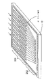
図1は、このような検出器の一部の例を示す模式図である。この実施形態では、半導体基板は、N型の結晶シリコンを含んでもよく、検出器は、検出器のエッジから衝突する入射X線101に対して、エッジオンで配向されてもよい。検出器の半導体基板102は、ストリップに分割され、各ストリップは、続いて、X線入射方向でもある深度方向内の複数の深度セグメントに分割される。各深度セグメントは、全体積がX線用の検出器として機能するように、完全に空乏化する必要がある、逆バイアスダイオードによって形成されてもよい。本実施形態において、ストリップ内の各深度セグメントは、ドープ領域107の上、例えばP+注入部の上に金属コンタクトが成膜された電荷収集側に、個別の電荷収集電極を有し、ドープ領域107は、ルーティングトレース103を介して、関連するフロントエンド電子回路に接続されている。電荷収集電極の金属コンタクトは、図1では、符号104が付与されている。金属の電荷収集電極の左列用のルーティングトレースのみが、図1に示されている。フロントエンド電子回路の一例は、特定用途向け集積回路、ASICである。ASICは、対応する電荷収集電極にそれぞれ接続された、複数の信号処理チャネルを含む。本実施形態において、電荷収集電極からフロントエンド電子回路まで信号を伝達するために用いられるルーティングトレース103は、図1に示される電荷収集電極の間の領域に延びるようにして配置される。検出器の電荷収集側は、本実施形態においては、したがって、単一金属層として設けられる。この特定の特徴は、ルーティングトレースのための余分な層の使用を不要にする。単一金属層のみを有する注入部の利点としては、より低いキャパシタンス、より高い形状効率性、および実施の複雑さを低下させることが挙げられる。図1からは、また、フロントエンド電子回路の入力が、検出器上の読み出しパッド105に取り付けられることが分かる。これは、ワイヤボンディング、バンプボンディング、または他の任意のマルチチップモジュール技術によって行うことができる。好適な実施形態において、フロントエンド電子回路は、ルーティングトレースが集まる検出器の底部エッジ12に取り付けられてもよい。
FIG. 1 is a schematic diagram showing an example of part of such a detector. In this embodiment, the semiconductor substrate may comprise N-type crystalline silicon and the detector may be oriented edge-on with respect to
提案技術の特定の実施形態によれば、半導体基板が、シリコンを含む、エッジオン検出器が提供される。 According to certain embodiments of the proposed technique, edge-on detectors are provided, wherein the semiconductor substrate comprises silicon.
提案技術の別の実施形態によれば、電荷収集金属電極104およびルーティングトレース103が、同じ金属から製造されたエッジオン検出器が提供される。すなわち、電荷収集金属電極104およびルーティングトレース103は、基板102の電荷収集側の単一金属層内に設けられる。電荷収集電極およびルーティングトレースに用いられる金属は、特定の実施形態において、アルミニウムであってもよい。
Another embodiment of the proposed technique provides an edge-on detector in which the charge
例として、提案技術に係るエッジオン検出器は、二酸化シリコンの絶縁領域106を備えてもよい。
As an example, an edge-on detector according to the proposed technology may comprise an
図2は、提案技術の例示的な実施形態に係る半導体基板、例えばシリコン基板、102の断面を示す模式図である。断面は、2つのストリップを有するエッジオン検出器を示しており、各ストリップは、2つの電荷収集電極と、その間の2つのルーティングトレース103とを有する。電荷収集電極の金属コンタクト104は、例えば、ルーティングトレースと同じ金属層上に延びるようにして、P+注入部上に形成されてもよい。薄い絶縁層、例えば二酸化シリコン層、106は、シリコン基板の表側でパシベーションとして用いられる。本実施形態において、バイアスが、N+注入部を通して裏面コンタクト108から供給され、検出器を完全に空乏化する。図2は、単なる例示であり、検出器は、より多くの詳細を含んでもよく、例えば、電荷収集側により多くのパシベーション層を含んでもよいことを、認識すべきである。
FIG. 2 is a schematic diagram illustrating a cross-section of a semiconductor substrate, eg, silicon substrate, 102, in accordance with an exemplary embodiment of the proposed technique. The cross-section shows an edge-on detector with two strips, each strip having two charge collection electrodes and two routing
幅狭の電荷収集電極は、キャパシタンスの観点から好適である。幅狭の電荷収集電極で得られる別の利点は、電荷収集電極間のルーティングトレースの適合を容易にすることである。 A narrow charge collection electrode is preferred from a capacitance standpoint. Another advantage provided by narrow charge collection electrodes is the ease of matching of routing traces between charge collection electrodes.
図3は、半導体基板、例えばシリコン基板、102の一部の模式図である。図3に示されているのは、図1の第3の深度セグメントの拡大図であり、電荷収集電極の金属コンタクト104と、ルーティングトレース103とが、同じ金属層で延びている。Pは、ストリップのピッチを表し、WEは、電荷収集電極の幅を表し、WTは、ルーティングトレースの幅を表すとすると、ストリップピッチに対する電極幅の比率は、次式により与えられる。
RE=WE/P
FIG. 3 is a schematic diagram of a portion of a semiconductor substrate, eg, silicon substrate, 102 . Shown in FIG. 3 is an enlarged view of the third depth segment of FIG. 1, where the
R E =W E /P
ストリップピッチに対するルーティングトレース幅の比率は、次式により与えられる。
RT=WT/P
The ratio of routing trace width to strip pitch is given by:
R T = W T /P
提案技術の特定の実施形態によれば、ストリップの数は、少なくとも2つであり、電荷収集金属電極の幅寸法は、ストリップピッチに対する電荷収集金属電極幅の比率が0.8未満であり、キャパシタンスを減少させるような寸法である、エッジオン検出器が提供される。 According to a particular embodiment of the proposed technology, the number of strips is at least two, the width dimension of the charge collection metal electrode is such that the ratio of charge collection metal electrode width to strip pitch is less than 0.8, and the capacitance An edge-on detector is provided that is dimensioned to reduce .
図4は、厚さ0.6mmのシリコン基板と、0.37mmのストリップピッチと、幅5μmのルーティングトレースとを有する検出器のためのストリップピッチに対する、電極幅の比率の関数としてシミュレートされたキャパシタンスを示している。3つの深度セグメントは、それぞれ10mm、15mmおよび20mmの深度セグメントの長さでシミュレートされている。その間に30%の接着剤および70%の空気を有する、シミュレートされた検出器の電荷収集側に対して20μm離れた、散乱防止シートとしての別の金属表面、あるいは別の電極の表面がある。比率が0.8未満の場合、キャパシタンスは比率に対してほぼ線形に比例するが、比率が0.8よりも大きい場合、キャパシタンスの大幅な増加がある。この結果は、他のストリップピッチに関して確認されている。 FIG. 4 was simulated as a function of the ratio of electrode width to strip pitch for a detector with a 0.6 mm thick silicon substrate, a 0.37 mm strip pitch, and a 5 μm wide routing trace. It shows capacitance. Three depth segments are simulated with depth segment lengths of 10 mm, 15 mm and 20 mm, respectively. Another metal surface as an anti-scatter sheet, or the surface of another electrode, 20 μm away to the charge collection side of the simulated detector with 30% glue and 70% air in between . For ratios less than 0.8, the capacitance is approximately linearly proportional to the ratio, but for ratios greater than 0.8, there is a significant increase in capacitance. This result has been confirmed for other strip pitches.
提案技術のさらに別の実施形態によれば、ストリップの数は、少なくとも2つであり、ルーティングトレースの幅寸法は、ストリップピッチに対するルーティングトレースの幅の比率が0.05未満であるような寸法である、エッジオン検出器が提供される。この実施形態は、改善されたキャパシタンス特性を有する、すなわち、減少されたキャパシタンスを示すエッジオン検出器を提供する。 According to yet another embodiment of the proposed technology, the number of strips is at least two and the width dimension of the routing trace is such that the ratio of the width of the routing trace to the strip pitch is less than 0.05. An edge-on detector is provided. This embodiment provides an edge-on detector with improved capacitance characteristics, ie, exhibiting reduced capacitance.
図5は、検出器のノイズレベルと、検出器キャパシタンスとの間のほぼ線形の関係を示している。したがって、比率REは、好ましくは、キャパシタンスおよび信号対ノイズ比の観点からの電荷収集電極の幅に関して、0.8未満であると結論づけられる。さらに、比率RTは、好ましくは、本実施形態におけるルーティングトレースの幅に関して、0.05未満であると結論づけることができる。 FIG. 5 shows a nearly linear relationship between detector noise level and detector capacitance. It is therefore concluded that the ratio RE is preferably less than 0.8 with respect to the width of the charge collection electrodes in terms of capacitance and signal-to-noise ratio. Furthermore, it can be concluded that the ratio R T is preferably less than 0.05 for the width of the routing traces in this embodiment.
より多くのルーティングトレースがその間で延びる、底部の深度セグメントに関して、隣接する電荷収集電極の間にルーティングトレースを適合させるために、より多くのスペースが必要とされる。ストリップピッチに対する、隣接する電荷収集電極の間の間隔の比率は、RG=WG/Pとして定義されるが、この比率は、好ましくは、深度セグメントの数をN≧2として、0.05×(N+1)よりも大きくすべきである。 For bottom depth segments, where more routing traces extend between them, more space is required to accommodate the routing traces between adjacent charge collection electrodes. The ratio of the spacing between adjacent charge collection electrodes to the strip pitch, defined as R G =W G /P, is preferably 0.05, with the number of depth segments N≧2. It should be greater than x(N+1).
シリコンと二酸化シリコンの間の界面の露出した領域は、注入部カバーなしでは放射線に感応するため、電荷収集電極は、極度に細くできないことを認識すべきである。したがって、キャパシタンスと検出器の放射線耐性との間に、トレードオフがある。 It should be recognized that the charge collection electrode cannot be extremely thin, since the exposed area of the interface between silicon and silicon dioxide is radiation sensitive without an implant cover. Therefore, there is a trade-off between capacitance and radiation tolerance of the detector.
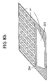
開示されたエッジオン検出器の別の実施形態によれば、半導体基板102には、第2の端部に配置された読み出しパッドに隣接した領域において、ドープ領域が設けられる。図8aは、この実施形態の模式図を提供する。読み出しパッドに隣接するドープ領域は、202で示され、一方で電荷収集電極が設けられるドープ領域を有する領域は、201で示される。ドープ領域は、この特定の図では、P+ドープ領域である。これはしかし、単なる例であり、他の種類のドーピングを用いてもよい。
According to another embodiment of the disclosed edge-on detector, the
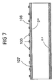
図1に示されるように、検出器の第2の端部において、ルーティングトレースは、読み出しパッドに接続されており、読み出しパッドは、その後、フロントエンド電子回路に接続されている。フロントエンド電子回路の入力に対するキャパシタンスを最小化するために、ルーティングトレースの長さを減少させ、ルーティングトレースをまばらに分散させるという必要条件がある。最後の電荷収集電極の端部で、検出器の大部分または検出器全体を覆うフロントエンド電子回路を有することが考えられる。しかし、フロントエンド電子回路の集積回路は、高速、低電力および低い製造コストのために、小型となる傾向があり、これは多くの場合、フロントエンド電子回路は、検出器の小さな部分しか覆うことができないことを意味する。小さな画素ピッチを有する検出器があり、この画素ピッチは、フロントエンド電子回路、例えば数十マイクロメートルの画素ピッチを有するマンモグラフィーの入力ピッチに相当する。このような検出器に対して、フロントエンド電子回路は、ルーティングトレースの最小長さを有し、よって最小のキャパシタンスを有する電荷収集電極に、非常に近接して接合することができる。しかし、大きな画素ピッチを有するいくつかのX線撮像検出器、例えばX線コンピュータ断層撮影もあり、ここでは、画素ピッチは、フロントエンド電子回路の入力ピッチよりもずっと大きい。このようなケースが、図6に示されており、ルーティングトレースは、検出器のX線検知部201のうちの一領域を占め、検出器の領域202内の読み出しパッドに集まり、扇形を形成する可能性が高い。ガードリング構造は、電荷収集側の特徴であり、この構造は、エッジ効果を最小化し、全てのストリップおよび深度セグメントに対して、定義された均質な電位の確保をもたらすために、特別に提供される。ガードリング構造は、図6に示されている。常にではないが、通常は、1つまたは複数のガードリングが、検出器のアクティブ部と検出器のエッジとの間に配置される。第1のリングは、特定の電位、通常はグランドに直接接続され、検出器のエッジに生成されるリーク電流のための排流を提供する。1つまたは複数の浮動リングがあり、電位を個別に適合させ、外部からの電圧効果を平滑にしてもよい。リングは、通常、ストリップおよび深度セグメントと同じ構造を、同じ種類の金属およびドーピングで有する。図6では、1つのリングの金属部分のみが示されている。
At the second end of the detector, the routing traces are connected to readout pads, which are then connected to the front-end electronics, as shown in FIG. In order to minimize the capacitance to the input of the front end electronics, there is a requirement to reduce the length of the routing traces and distribute the routing traces sparsely. At the end of the last charge collection electrode, it is conceivable to have front end electronics covering most of the detector or the entire detector. However, integrated circuits for front-end electronics tend to be small due to their high speed, low power and low manufacturing cost, which often means that the front-end electronics cover only a small portion of the detector. means that you cannot There are detectors with a small pixel pitch, which corresponds to the input pitch of front-end electronics, for example mammography, which has a pixel pitch of a few tens of micrometers. For such detectors, the front-end electronics have a minimum length of routing traces and can therefore be joined very closely to the charge collection electrodes with minimum capacitance. However, there are also some X-ray imaging detectors, such as X-ray computed tomography, that have a large pixel pitch, where the pixel pitch is much larger than the input pitch of the front-end electronics. Such a case is illustrated in FIG. 6, where the routing traces occupy an area of the x-ray
図7は、例示的な実施形態に係る、シリコン基板の読み出しパッドに隣接する領域の例示的な断面を示す模式図である。ルーティングトレースCは、二酸化シリコンを含む絶縁層106の上を延びている。常にではないが、通常は、絶縁層106は、読み出しパッドに隣接する領域全体を覆う。請求される本発明の一実施形態においては、二酸化シリコンの下で、N型結晶シリコンを用いて、検出器のガードリングから延びるP+注入部203は、通常、底部領域全体を覆うが、しかしこれは、ルーティングトレースと、二酸化シリコンの典型的な厚さを与えられたP+注入部の層との間に、高いキャパシタンスを生じる。
FIG. 7 is a schematic diagram illustrating an exemplary cross-section of a region adjacent to a readout pad of a silicon substrate, according to an exemplary embodiment. A routing trace C extends over an insulating
開示されたエッジオン検出器の別の実施形態によれば、半導体基板Bには、第2の端部に配置された読み出しパッドに隣接する領域に、ドープ領域が設けられる。図8aは、この実施形態の模式図を提供する。この実施形態においては、ドープ領域は、読み出しパッドに隣接する領域全体を覆う。ドープ領域は、この特定の図では、P+ドープ領域である。しかしこれは、これは単なる例であり、他の種類のドーピングを用いてもよい。 According to another embodiment of the disclosed edge-on detector, the semiconductor substrate B is provided with a doped region in a region adjacent to the readout pad arranged at the second end. Figure 8a provides a schematic of this embodiment. In this embodiment, the doped region covers the entire area adjacent to the read pad. The doped regions are P+ doped regions in this particular illustration. However, this is only an example and other types of doping may be used.
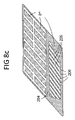
別の実施形態は、読み出しパッドに隣接する領域に、絶縁領域がさらに設けられ、これにより、ドープ領域と絶縁領域とが配置されて、ルーティングトレースが絶縁領域上を読み出しパッドまで延びるようなパターンを形成する、エッジオン検出器を提供する。このようなパターンの特定の例が、図8bおよび図8cに与えられている。図8bでは、絶縁領域203の領域が、どのようにしてドープ領域204に囲まれているかを示している。不図示のルーティングトレース103は、絶縁領域の上に配置されることを意図している。図8cでは、絶縁領域を、どのようにして読み出しパッドに隣接する領域に配置して、ルーティングトレースを、扇状のやり方で読み出しパッドに接続し得るかを示している。
Another embodiment further provides an isolation region in the region adjacent to the read pad such that the doped region and the isolation region are arranged in a pattern such that the routing traces extend over the isolation region to the read pad. forming an edge-on detector; A specific example of such a pattern is given in Figures 8b and 8c. In FIG. 8b it is shown how regions of insulating
図8a~図8cは、図6に示されるセンサのための注入層の異なる実施に対応する模式図であり、検出器の読み出しパッドに隣接する領域で延びる、ルーティングトレースからのキャパシタンスに対処する異なる方策を示している。X線検知部201は、電荷収集電極のP+注入部、図2のP+を含み、検出器の第2の端部に近い領域202も、P+注入領域、図7のP+を含む。
8a-c are schematic diagrams corresponding to different implementations of injection layers for the sensor shown in FIG. shows the strategy. The
請求される本発明の一実施形態において、図8aに示すように、非注入領域に囲まれる、注入層上の電荷収集電極の注入部がある。ガードリングの注入部から延びる注入領域は、センサの第2の端部の読み出しパッドに隣接する領域全体を覆い、これは結果として、本実施形態において、比較的高いキャパシタンスをもたらす。ガードリング構造の1つのリングのみが、図示されている。 In one embodiment of the claimed invention, there is an injection portion of the charge collection electrode on the injection layer surrounded by non-injection regions, as shown in FIG. 8a. The implanted region extending from the guard ring implant covers the entire area adjacent to the readout pad at the second end of the sensor, which in this embodiment results in a relatively high capacitance. Only one ring of the guard ring structure is shown.
請求される本発明の別の実施形態において、図8bに示すように、センサの底部領域で、注入領域は、ガードリングから、最も外側のトレースのみに近接してさらに延びており、これにより、203で示される、トレースの下の領域に対しては、注入部はない。電荷収集電極の近くに、長いストリップ注入領域204があり、センサのガードリングに接続されて、センサのガードリングに対する、センサの第2の端部の領域内で生成されたリーク電流をガイドし、センサの第2の端部の領域内で生じた障害がX線検知部に達することを防止する。本実施形態は、センサの第2の端部の領域内で延びるルーティングトレースにより誘発されるキャパシタンスを、少なくとも有するものとしている。
In another embodiment of the claimed invention, as shown in FIG. 8b, in the bottom region of the sensor, the implanted region further extends from the guard ring and close to only the outermost traces, thereby: For the area under the trace, indicated at 203, there are no implants. near the charge collection electrode is a long
センサの第2の端部の領域内で、ルーティングトレースとP+注入部との間で誘発されるキャパシタンスを減少させ、リーク電流、ブレークダウン電圧などの、センサの他の側面を、前の実施形態と比較して高信頼かつ制御下に保つために、別の実施形態が提供される。図8cは、読み出しパッドに隣接する領域内で、非注入領域206により分離されるP+注入部205のストリップパターンを示す模式図である。P+注入ストリップは、センサのガードリングに接続される。この例では、注入ストリップは、センサ深度方向に沿って電荷収集電極に対して平行であるが、注入ストリップは、他の方向、例えば、電荷収集電極に垂直、またはグリッドパターンを形成する両方向、あるいは他の任意のパターンに沿うこともできる。センサの第2の端部で読み出しパッドに隣接する領域内で、ルーティングトレースにより誘発されるキャパシタンスは、P+注入部の領域を減少させることにより、相応に減少される。注入ストリップの幅をaで表し、非注入部間隔の幅をbで表すと、キャパシタンスは、これにより、ほぼ、b/(a+b)に減少させることができる。さらにキャパシタンスを減少させるために、本発明の特定の実施形態では、注入ストリップ間の非注入領域を、ルーティングトレースの経路を追うように配置することができ、これは、ルーティングトレースとP+注入部との間のより少ない重複と、よってより少ないキャパシタンスとをもたらす。
In the region of the second end of the sensor, the capacitance induced between the routing traces and the P+ implant is reduced, and other aspects of the sensor, such as leakage current, breakdown voltage, etc., are reduced to those of the previous embodiment. Another embodiment is provided to keep it reliable and under control compared to. FIG. 8c is a schematic diagram showing a strip pattern of
1列のみの読み出しパッドを、上述の実施形態にて示したが、複数列の読み出しパッドも、当業者には明らかであろう。 Although only one column of readout pads is shown in the above embodiments, multiple columns of readout pads will be apparent to those skilled in the art.
提案技術は、また、半導体基板が、テーパ形状を有し、これにより、半導体基板の第1の端部11が、第1の幅を有し、半導体基板の第2の端部12が、第1の端部よりも大きな第2の幅を有する、エッジオン検出器を提供する。このようなエッジオン検出器は、電荷収集金属電極の少なくとも2つのストリップを備えた半導体基板を含んでもよく、ストリップは、電荷収集電極が、基板のテーパ形状に適合されたテーパパターン内の電荷収集側に設けられるように、互いに対して角度をなしている。
The proposed technique also provides that the semiconductor substrate has a tapered shape such that the
これらのような設計は、大型のセンサが利用される場合に、特に有用となり得る。図9に示されるように、設計の図が提供される。図9において、各個別の深度セグメントは、X線101の入射方向に沿って、X線源を指すように傾けて配置されることが分かる。センサの台形形状は、例示的な実施形態を形成する。このようなセンサの台形形状は、センサの四角形状と比べて最小のデッドスペースを有してセンサを並べて搭載することにより、検出器の幅を延ばすことを容易にするが、その理由は、X線源を指すように各センサを配置する必要もあるためである。しかし、大型のセンサの四角形状も、請求される本発明によってカバーされることを、認識すべきである。
Designs such as these can be particularly useful when large sensors are utilized. A diagram of the design is provided as shown in FIG. It can be seen in FIG. 9 that each individual depth segment is tilted along the direction of incidence of the
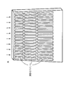
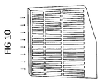
提案技術は、また、基板の第2の端部が、少なくとも1つの面取り角部を備えた、エッジオン検出器を提供する。図10は、1つの角部を取り除いてセンサの面取り形状を生成した、センサの別の例を示す模式図であり、このセンサは、最も近いセンサから誘発されるキャパシタンスを減少させ、かつ、回路のボンディング接続のためにより多くのスペースを割り当てることによって、フロントエンド電子回路の搭載も容易にする。フロントエンド電子回路を、ワイヤボンディング、フリップフロップ技術を用いたバンプボンディング、または他の任意のボンディング技術によりセンサに接続して、マルチチップモジュールを形成することができる。 The proposed technique also provides an edge-on detector in which the second edge of the substrate comprises at least one chamfered corner. FIG. 10 is a schematic diagram showing another example of a sensor with one corner removed to create a chamfered shape for the sensor, which reduces the capacitance induced from the closest sensor, and the circuit It also facilitates the mounting of front-end electronics by allocating more space for bonding connections. The front-end electronics can be connected to the sensor by wire bonding, bump bonding using flip-flop technology, or any other bonding technique to form a multi-chip module.
上述したように、提案技術は、キャパシタンス特性を改善したエッジオン半導体ストリップ検出器を提供する。ストリップ検出器は、40keV~250keVのエネルギー範囲内でのX線撮像における使用に適している。このような検出器の特定の特徴は、単一金属層を、検出器の電荷収集側に実装可能なことである。この単一層は、導電ルーティングトレースと、電荷収集電極とを備える。この特定の特徴は、改善されたキャパシタンス特性を有する検出器を提供する。提案技術は、したがって、このようなエッジオン検出器の電荷収集側を製造する方法を提供する。 As mentioned above, the proposed technique provides an edge-on semiconductor strip detector with improved capacitance characteristics. Strip detectors are suitable for use in X-ray imaging within the energy range of 40 keV to 250 keV. A particular feature of such detectors is that a single metal layer can be implemented on the charge collection side of the detector. This single layer comprises conductive routing traces and charge collection electrodes. This particular feature provides a detector with improved capacitance characteristics. The proposed technique therefore provides a method of manufacturing the charge collection side of such an edge-on detector.
このために、エッジオン検出器のための電荷収集面を製造するための方法が提供され、この方法は、
- X線源に対向するように構成された第1の端部と、第1の端部の反対側の第2の端部と、を有する半導体基板102を供給するステップS1と、
- 電荷収集面と称される、半導体基板102の表面に、ドープ領域107を設けるステップS2と、
- ドープ領域107が設けられていない第2の表面の領域の上に、絶縁層106を設けるステップS3と、
- 半導体基板の第2の端部に、読み出しパッド105を配置するステップS4と、
- ドープ領域107と、絶縁層とを備える電荷収集面の上に、単一金属層を成膜するステップS5と、
- 単一金属層をパターニングして、
i) ドープ領域107の上に、電荷収集金属電極を形成し、
ii) 絶縁層106の上に、電荷収集金属電極を読み出しパッド105と接続するルーティングトレース103を形成するステップS6と、
を含む。
To this end, a method is provided for manufacturing a charge collection surface for an edge-on detector, the method comprising:
- a step S1 of providing a
- a step S2 of providing a doped
- a step S3 of providing an insulating
- a step S4 of placing a
- a step S5 of depositing a single metal layer on the charge collecting surface comprising the doped
- by patterning a single metal layer,
i) forming a charge collection metal electrode over the doped
ii) step S6 of forming routing traces 103 on the insulating
including.
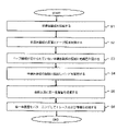
提案された方法は、図16のフロー図に、模式的に示されている。 The proposed method is illustrated schematically in the flow diagram of FIG.
提案された方法の特定の実施形態によれば、単一金属層を成膜するステップS5は、物理蒸着法(PVD)、めっき法および/または化学蒸着法(CVD)を使用することを含む。 According to a particular embodiment of the proposed method, the step S5 of depositing a single metal layer comprises using physical vapor deposition (PVD), plating and/or chemical vapor deposition (CVD).
提案された方法の別の特定の実施形態によれば、単一金属層をパターニングするステップS6は、フォトリソグラフィの使用を含む。 According to another particular embodiment of the proposed method, the step S6 of patterning the single metal layer comprises using photolithography.
提案技術のさらに別の実施形態は、半導体基板102を供給するステップS1は、シリコン基板を供給することを含む。
Yet another embodiment of the proposed technique, the step S1 of providing a
提案技術のさらに別の実施形態は、電荷収集面の上に、単一金属層を成膜するステップS5は、単一アルミニウム層を成膜することを含む方法を提供する。いくつかの金属層を、第1の金属層の上に成膜してもよいことに留意すべきである。例えば、提案された方法を行い、初回は、パターニングされてルーティングトレースと電荷収集電極とを形成した第1の金属層を有する電荷収集側を得、次いで、成膜ステップを1または複数回繰り返し、互いの上に配置された電荷収集電極とルーティングトレースとを形成するいくつかの金属層を得てもよい。 Yet another embodiment of the proposed technology provides a method wherein the step S5 of depositing a single metal layer on the charge collecting surface comprises depositing a single aluminum layer. It should be noted that several metal layers may be deposited over the first metal layer. For example, performing the proposed method, first obtaining a charge collection side having a first metal layer patterned to form routing traces and charge collection electrodes, and then repeating the deposition step one or more times, Several metal layers may be obtained forming charge collection electrodes and routing traces arranged on top of each other.
提案技術の任意の実施形態によれば、ドープ領域107が設けられていない第2の表面の領域上に、絶縁層106を設けるステップS3は、二酸化シリコン層を設けることを含む方法が提供される。
According to any embodiment of the proposed technology, a method is provided in which the step S3 of providing an insulating
提案技術の特定の実施形態によれば、金属層をパターニングするステップS6は、電荷収集電極の少なくとも2つのストリップを形成することを含み、電荷収集電極のそれぞれは、ストリップピッチに対する電荷収集金属電極幅の比率が、0.8未満であるような幅寸法を有する方法が提供される。 According to a particular embodiment of the proposed technique, the step S6 of patterning the metal layer includes forming at least two strips of charge collecting electrodes, each of the charge collecting electrodes having a charge collecting metal electrode width with respect to the strip pitch. is less than 0.8.
提案技術の別の実施形態は、金属層をパターニングするステップS6は、ストリップピッチに対するルーティングトレース幅の比率が、0.05未満であるような幅寸法を有するルーティングトレースを形成することをさらに含む方法を提供する。 Another embodiment of the proposed technique is the method in which the step S6 of patterning the metal layer further comprises forming the routing traces having width dimensions such that the ratio of routing trace width to strip pitch is less than 0.05. I will provide a.
提案技術は、また、上述の方法に従って製造された電荷収集面を備えるエッジオン検出器を提供する。 The proposed technique also provides an edge-on detector comprising a charge collecting surface manufactured according to the method described above.
本開示に示される実施形態は、N型結晶シリコンによる例を示しているが、提案技術は、N+ドープ電極を有するP型結晶シリコンにも適用できることを認識すべきである。センサ形状の変形は、当業者に対して直ちに明らかとなることを、認識すべきである。したがって、添付の特許請求の範囲は、例えば、センサの三角形形状または2つの面取りされた角部を有するセンサなど、すべてのこのような変形および修正を含むように、可能な限り広く解釈されることを意図している。加えて、深度セグメントの異なる数およびセグメント長さの異なる変更例が、請求される本発明の範囲に含まれる。 Although the embodiments shown in this disclosure show examples with N-type crystalline silicon, it should be recognized that the proposed techniques are also applicable to P-type crystalline silicon with N+ doped electrodes. It should be recognized that variations in sensor geometry will be readily apparent to those skilled in the art. It is therefore intended that the appended claims be interpreted as broadly as possible to include all such variations and modifications, for example, a triangular shape of the sensor or a sensor with two chamfered corners. is intended. Additionally, different numbers of depth segments and different variations of segment lengths are within the scope of the claimed invention.
参考文献
・ R.ノヴォトニー(R. Nowotny)、“医学および構造解析におけるSiマイクロストリップ検出器の応用(Application of Si-microstrip-detectors in medicine and structural analysis)”、物理学研究における核計器および方法(Nuclear Instruments and Methods in Physics Research)226(1984)34~39
・ 米国特許第4,937,453号、ロバート・ネルソン(Robert Nelson)“放射線撮像用X線検出器(X-ray detector for radiographic imaging)”
・ 米国特許第5,434,417号、デイビッド・ナイグレン(David Nygren)“高解像度エネルギーに敏感なデジタルX線(High resolution energy-sensitive digital X-ray)”
・ 米国特許第7,291,841号B2、ロバート・ネルソン(Robert Nelson)ら、“核医学における強化されたSPECT、PET、およびコンプトン散乱撮像のための装置およびシステム(Device and system for enhanced SPECT, PET, and Compton scatter imaging in nuclear medicine)”
・ ショウイチ・ヨシダ(Shoichi Yoshida)、タカシ・オオスギ(Takashi Ohsugi)、“シリコンストリップ検出器のX線コンピュータ断層撮影への応用(Application of silicon strip detectors to X-ray computed tomography)”、物理学研究における核計器および方法(Nuclear Instruments and Methods in Physics Research)、A 541(2005)、412~420
・ 米国特許第8,183,535号B2、マッツ・ダニエルソン(Mats Danielsson)ら、“X線撮像用のシリコン検出器アセンブリ(Silicon detector assembly for x-ray imaging)”
・ チェン・シュウ(Cheng Xu)ら、“光子計数スペクトルCT用のセグメント化シリコンストリップ検出器のエネルギー分解能(Energy resolution of a segmented silicon strip detector for photon-counting spectral CT)”、物理学研究における核計器および方法(Nuclear Instruments and Methods in Physics Research)、A715(2013)、11~17
・ スジン・リウ(Xuejin Liu)ら、“マルチビン光子計数スペクトルコンピューター断層撮影検出器用のスペクトル応答モデルとその応用(Spectral response model for a multibin photon-counting spectral computed tomography detector and its applications)”、医用画像ジャーナル(Journal of Medical Imaging)2(3)(2015)033502
・ スウェーデン特許出願第9801677-7号、マッツ・ダニエルソン(Mats Danielsson)
・ “シリコンストリップ検出器での電荷収集(Charge collection in silicon strip detectors)”、物理学研究における核計器および方法(Nuclear Instruments and Methods in Physics Research)214(2-3)(1983)、253~260
References R. R. Nowotny, "Application of Si-microstrip-detectors in medicine and structural analysis," Nuclear Instruments and Methods in Physics Research Physics Research) 226 (1984) 34-39
- US Pat. No. 4,937,453, Robert Nelson "X-ray detector for radiographic imaging";
- US Pat. No. 5,434,417, David Nygren, "High resolution energy-sensitive digital X-ray";
- U.S. Pat. No. 7,291,841 B2, Robert Nelson et al., "Device and system for enhanced SPECT, PET, and Compton scatter imaging in nuclear medicine." PET, and Compton scatter imaging in nuclear medicine)”
Shoichi Yoshida, Takashi Ohsugi, "Application of silicon strip detectors to X-ray computed tomography," in physics research. Nuclear Instruments and Methods in Physics Research, A 541 (2005), 412-420
- US Pat. No. 8,183,535 B2, Mats Danielsson et al., "Silicon detector assembly for x-ray imaging"
Cheng Xu et al., “Energy resolution of a segmented silicon strip detector for photon-counting spectral CT,” Nuclear Instruments in Physics Research. and Methods (Nuclear Instruments and Methods in Physics Research), A715 (2013), 11-17
Xuejin Liu, et al., “Spectral response model for a multibin photon-counting spectral computed tomography detector and its applications,” Journal of Medicine. (Journal of Medical Imaging) 2(3) (2015) 033502
- Swedish Patent Application No. 9801677-7, Mats Danielsson
"Charge collection in silicon strip detectors", Nuclear Instruments and Methods in Physics Research 214(2-3) (1983), 253-260.
Claims (15)
- X線源に対向するように構成された第1の端部と、入射X線の方向において、前記第1の端部の反対側にある第2の端部と、
- N≧2とするN個の深度セグメントを有し、前記深度セグメントのそれぞれが、電荷収集金属電極を備える、少なくとも1つのストリップと、
- ドープ領域と絶縁領域とを備えた電荷収集側と、を備え
前記電荷収集金属電極のそれぞれは、対応するドープ領域の上に配置され、前記絶縁領域上に配置された、それぞれのルーティングトレースに接続され、それぞれの前記ルーティングトレースは、前記電荷収集金属電極から、前記第2の端部に配置されたフロントエンド電子回路に接続可能な読み出しパッドへと信号を伝達するように構成され、
前記ストリップの数は、少なくとも2つであり、
前記電荷収集金属電極の幅寸法は、ストリップピッチに対する前記電荷収集金属電極幅の比率が0.8未満であり、キャパシタンスを減少させるような寸法である、エッジオン光子計数検出器。 An edge-on photon counting detector comprising a semiconductor substrate, the semiconductor substrate comprising:
- a first end configured to face the X-ray source and a second end opposite said first end in the direction of the incident X-rays;
- at least one strip having N depth segments, where N≧2, each of said depth segments comprising a charge collecting metal electrode;
a charge collecting side comprising a doped region and an insulating region, each of said charge collecting metal electrodes disposed over a corresponding doped region and to a respective routing trace disposed over said insulating region; each said routing trace connected and configured to carry a signal from said charge collecting metal electrode to a readout pad connectable to front end electronics located at said second end ;
the number of strips is at least two;
An edge-on photon counting detector , wherein the width dimension of the charge collection metal electrode is dimensioned such that the ratio of the charge collection metal electrode width to strip pitch is less than 0.8 to reduce capacitance .
前記ルーティングトレースの幅寸法は、ストリップピッチに対する前記ルーティングトレース幅の比率が0.05未満であり、キャパシタンスを減少させるような寸法である、請求項1から6のいずれか1項に記載のエッジオン検出器。 the number of strips is at least two;
Edge-on detection according to any one of claims 1 to 6 , wherein the width dimension of the routing trace is dimensioned such that the ratio of the routing trace width to strip pitch is less than 0.05 to reduce capacitance. vessel.
- X線源に対向するように構成された第1の端部と、前記第1の端部の反対側にある第2の端部と、を有する半導体基板を供給するステップ(S1)と、
- 電荷収集面と称される、前記半導体基板の表面に、ドープ領域を設けるステップ(S2)と、
- ドープ領域が設けられていない第2の表面の領域に、絶縁層を設けるステップ(S3)と、
- 前記半導体基板の前記第2の端部に、読み出しパッドを配置するステップ(S4)と、
- 前記ドープ領域と、前記絶縁層とを備える前記電荷収集面の上に、単一金属層を成膜するステップ(S5)と、
- 前記単一金属層をパターニングして、
i)前記ドープ領域の上に、電荷収集金属電極を形成し、
ii)前記絶縁層の上に、前記電荷収集金属電極を前記読み出しパッドと接続するルーティングトレースを形成するステップ(S6)と、
を含み、
ドープ領域(R)が設けられていない前記第2の表面の領域に、絶縁層Fを設けるステップ(S3)は、二酸化シリコン層を設けることを含み、
前記金属層をパターニングする前記ステップ(S6)は、電荷収集金属電極の少なくとも2つのストリップを形成することを含み、前記電荷収集金属電極のそれぞれは、ストリップピッチに対する電荷収集金属電極幅の比率が、0.8未満であるような幅寸法を有する、方法。 A method for manufacturing a charge collection surface for an edge-on detector, comprising:
- providing (S1) a semiconductor substrate having a first end configured to face an X-ray source and a second end opposite said first end;
- providing a doped region (S2) on the surface of the semiconductor substrate, called charge collection surface;
- providing an insulating layer (S3) in areas of the second surface not provided with doped regions;
- disposing (S4) a readout pad at the second end of the semiconductor substrate;
- depositing (S5) a single metal layer on the charge collecting surface comprising the doped regions and the insulating layer;
- patterning said single metal layer,
i) forming a charge collecting metal electrode over the doped region;
ii) forming routing traces on the insulating layer connecting the charge collection metal electrodes with the readout pads (S6);
including
The step (S3) of providing an insulating layer F in regions of said second surface not provided with doped regions (R) comprises providing a silicon dioxide layer,
Said step (S6) of patterning said metal layer includes forming at least two strips of charge collecting metal electrodes, each of said charge collecting metal electrodes having a ratio of charge collecting metal electrode width to strip pitch of: A method having a width dimension such that it is less than 0.8 .
前記電荷収集面の上に単一金属層を成膜する前記ステップ(S5)は、物理蒸着法(PVD)、めっき法および/または化学蒸着法(CVD)を使用して単一アルミニウム層を成膜することを含み、
前記単一金属層をパターニングするステップ(S6)は、フォトリソグラフィの使用を含む、請求項13に記載の方法。 The step (S1) of supplying a semiconductor substrate B includes supplying a silicon substrate,
Said step (S5) of depositing a single metal layer on said charge collection surface uses physical vapor deposition (PVD), plating and/or chemical vapor deposition (CVD) to deposit a single aluminum layer. including filming;
14. The method of claim 13 , wherein patterning (S6) the single metal layer comprises using photolithography.
Applications Claiming Priority (3)
| Application Number | Priority Date | Filing Date | Title |
|---|---|---|---|
| US15/595,087 | 2017-05-15 | ||
| US15/595,087 US10126437B1 (en) | 2017-05-15 | 2017-05-15 | Detector for x-ray imaging |
| PCT/SE2018/050475 WO2018212698A1 (en) | 2017-05-15 | 2018-05-08 | Detector for x-ray imaging |
Publications (2)
| Publication Number | Publication Date |
|---|---|
| JP2020521953A JP2020521953A (en) | 2020-07-27 |
| JP7127066B2 true JP7127066B2 (en) | 2022-08-29 |
Family
ID=64050884
Family Applications (1)
| Application Number | Title | Priority Date | Filing Date |
|---|---|---|---|
| JP2019563170A Active JP7127066B2 (en) | 2017-05-15 | 2018-05-08 | Detector for X-ray imaging |
Country Status (7)
| Country | Link |
|---|---|
| US (2) | US10126437B1 (en) |
| EP (1) | EP3625592B1 (en) |
| JP (1) | JP7127066B2 (en) |
| KR (1) | KR102470183B1 (en) |
| CN (1) | CN110678782B (en) |
| IL (1) | IL270520B (en) |
| WO (1) | WO2018212698A1 (en) |
Families Citing this family (9)
| Publication number | Priority date | Publication date | Assignee | Title |
|---|---|---|---|---|
| JP6893135B2 (en) * | 2017-07-07 | 2021-06-23 | フォンダチオーネ ブルーノ ケスラー | Radiation detector, radiation detector and radiation detector |
| US10813607B2 (en) * | 2018-06-27 | 2020-10-27 | Prismatic Sensors Ab | X-ray sensor, method for constructing an x-ray sensor and an x-ray imaging system comprising such an x-ray sensor |
| CN109490944B (en) * | 2018-11-22 | 2022-11-04 | 天津大学 | Energy analysis method of x-ray energy spectrum detector |
| EP3690490A1 (en) * | 2019-02-04 | 2020-08-05 | ams International AG | X-ray detector component, x-ray detection module, imaging device and method for manufacturing an x-ray detector component |
| CN110176519B (en) * | 2019-06-17 | 2021-08-06 | 京东方科技集团股份有限公司 | Flat panel detector and method of making the same |
| US11389125B1 (en) * | 2021-02-05 | 2022-07-19 | GE Precision Healthcare LLC | System and method for mitigating trace triggering of channels in x-ray detector |
| CN114447149B (en) * | 2022-01-11 | 2023-12-01 | 上海奕瑞光电子科技股份有限公司 | Edge incidence detector and manufacturing method thereof |
| US12471877B2 (en) * | 2022-06-07 | 2025-11-18 | GE Precision Healthcare LLC | Photon counting computed tomography (PCCT) detector sensor repair for increased sensor yield |
| US12493128B2 (en) * | 2023-08-09 | 2025-12-09 | GE Precision Healthcare LLC | Medical imaging detector |
Citations (2)
| Publication number | Priority date | Publication date | Assignee | Title |
|---|---|---|---|---|
| JP2007007407A (en) | 2005-06-29 | 2007-01-18 | General Electric Co <Ge> | Multi-layer direct conversion computed tomography detector module |
| JP2011145292A (en) | 2010-01-13 | 2011-07-28 | Fei Co | Radiation detector |
Family Cites Families (21)
| Publication number | Priority date | Publication date | Assignee | Title |
|---|---|---|---|---|
| US4937453A (en) | 1987-05-06 | 1990-06-26 | Nelson Robert S | X-ray detector for radiographic imaging |
| US5434417A (en) | 1993-11-05 | 1995-07-18 | The Regents Of The University Of California | High resolution energy-sensitive digital X-ray |
| US5528043A (en) * | 1995-04-21 | 1996-06-18 | Thermotrex Corporation | X-ray image sensor |
| SE518811C2 (en) | 1998-05-13 | 2002-11-26 | Mamea Imaging Ab | Radiation detector for calibrating and verifying radiosurgical equipment, contains several detector elements each producing individual induced currents for creating multi dimensional radiation dose distribution |
| US6546075B1 (en) * | 1999-05-10 | 2003-04-08 | Epsirad Inc. | Energy sensitive detection systems |
| WO2004031803A1 (en) * | 2002-10-07 | 2004-04-15 | Sunnybrook And Women's College Health Sciences Centre | High quantum efficiency x-ray detector for portal imaging |
| US7291841B2 (en) | 2003-06-16 | 2007-11-06 | Robert Sigurd Nelson | Device and system for enhanced SPECT, PET, and Compton scatter imaging in nuclear medicine |
| US7635848B2 (en) * | 2005-04-01 | 2009-12-22 | San Diego State University Research Foundation | Edge-on SAR scintillator devices and systems for enhanced SPECT, PET, and compton gamma cameras |
| JP2009059975A (en) | 2007-09-03 | 2009-03-19 | Mitsubishi Electric Corp | Photosensor and X-ray imaging apparatus |
| FI121828B (en) * | 2007-12-04 | 2011-04-29 | Finphys Oy | Radiation detector, method of producing a radiation detector and use of the detector for measuring radiation |
| US8183535B2 (en) * | 2009-02-11 | 2012-05-22 | Mats Danielsson | Silicon detector assembly for X-ray imaging |
| JP2011238897A (en) | 2010-04-13 | 2011-11-24 | Canon Inc | Detection device, manufacturing method thereof, and detection system |
| JP5711476B2 (en) | 2010-07-29 | 2015-04-30 | 日立アロカメディカル株式会社 | Radiation detector card |
| JP5569842B2 (en) * | 2010-08-04 | 2014-08-13 | 日立アロカメディカル株式会社 | Radiation detector and radiation detection apparatus |
| GB2491111B (en) * | 2011-05-19 | 2015-08-19 | Oxford Instr Nanotechnology Tools Ltd | Charge-sensitive amplifier |
| US8445853B2 (en) * | 2011-08-22 | 2013-05-21 | Eastman Kodak Company | Method of making a radiation-sensitive substrate |
| RU2015110023A (en) * | 2012-08-23 | 2016-10-10 | Конинклейке Филипс Н.В. | SEMICONDUCTOR PHOTON ACCOUNT DETECTORS |
| WO2014131949A1 (en) * | 2013-02-28 | 2014-09-04 | Sensor Systems Group Inc. Oy | Detector for detecting neutrons and x- and gamma ray photons |
| GB2516034A (en) | 2013-07-08 | 2015-01-14 | Plastic Logic Ltd | Radiation imaging |
| JP2015133408A (en) * | 2014-01-14 | 2015-07-23 | 株式会社島津製作所 | Radiation detector |
| US10561382B2 (en) * | 2014-12-19 | 2020-02-18 | G-Ray Switzerland Sa | Photon counting cone-beam CT apparatus with monolithic CMOS integrated pixel detectors |
-
2017
- 2017-05-15 US US15/595,087 patent/US10126437B1/en active Active
-
2018
- 2018-03-15 US US15/922,389 patent/US10386506B2/en active Active
- 2018-05-08 EP EP18801801.4A patent/EP3625592B1/en active Active
- 2018-05-08 KR KR1020197035106A patent/KR102470183B1/en active Active
- 2018-05-08 WO PCT/SE2018/050475 patent/WO2018212698A1/en not_active Ceased
- 2018-05-08 JP JP2019563170A patent/JP7127066B2/en active Active
- 2018-05-08 CN CN201880032096.6A patent/CN110678782B/en active Active
-
2019
- 2019-11-07 IL IL270520A patent/IL270520B/en active IP Right Grant
Patent Citations (2)
| Publication number | Priority date | Publication date | Assignee | Title |
|---|---|---|---|---|
| JP2007007407A (en) | 2005-06-29 | 2007-01-18 | General Electric Co <Ge> | Multi-layer direct conversion computed tomography detector module |
| JP2011145292A (en) | 2010-01-13 | 2011-07-28 | Fei Co | Radiation detector |
Non-Patent Citations (1)
| Title |
|---|
| CHENG,Xu et al.,Energy resolution of a segmented silicon strip detector for photon-counting spectral CT,Nuclear Instruments & Methods in Physics Research, Section A.,米国,2013年,A715,p.11-17 |
Also Published As
| Publication number | Publication date |
|---|---|
| IL270520B (en) | 2021-04-29 |
| EP3625592B1 (en) | 2025-06-25 |
| US20180329082A1 (en) | 2018-11-15 |
| CN110678782A (en) | 2020-01-10 |
| KR102470183B1 (en) | 2022-11-23 |
| EP3625592A1 (en) | 2020-03-25 |
| US10126437B1 (en) | 2018-11-13 |
| US10386506B2 (en) | 2019-08-20 |
| CN110678782B (en) | 2023-06-13 |
| US20180329083A1 (en) | 2018-11-15 |
| JP2020521953A (en) | 2020-07-27 |
| EP3625592A4 (en) | 2021-02-24 |
| WO2018212698A1 (en) | 2018-11-22 |
| KR20200006071A (en) | 2020-01-17 |
Similar Documents
| Publication | Publication Date | Title |
|---|---|---|
| JP7127066B2 (en) | Detector for X-ray imaging | |
| CN102224434B (en) | Silicon detector assembly for x-ray imaging | |
| JP5555491B2 (en) | Radiation detector having a plurality of electrodes on a photosensitive layer | |
| CN103917897B (en) | There is the radiation-sensitive detector equipment of the intersegmental gap of electrical charge rejection | |
| US11054532B2 (en) | X-ray detector system design | |
| US20100252744A1 (en) | Radiation detector with a plurality of electrode systems | |
| CN113167917B (en) | X-ray imaging system using photon counting events for phase contrast imaging | |
| CN113039459A (en) | Method and system for estimating initial interaction point of X-ray photon in photon counting X-ray detector | |
| US12232897B2 (en) | System and method for mitigating trace triggering of channels in X-ray detector | |
| JP7679417B2 (en) | Collimator assembly for X-ray detector |
Legal Events
| Date | Code | Title | Description |
|---|---|---|---|
| A521 | Request for written amendment filed |
Free format text: JAPANESE INTERMEDIATE CODE: A523 Effective date: 20200116 |
|
| A621 | Written request for application examination |
Free format text: JAPANESE INTERMEDIATE CODE: A621 Effective date: 20210329 |
|
| A977 | Report on retrieval |
Free format text: JAPANESE INTERMEDIATE CODE: A971007 Effective date: 20220323 |
|
| A131 | Notification of reasons for refusal |
Free format text: JAPANESE INTERMEDIATE CODE: A131 Effective date: 20220412 |
|
| A521 | Request for written amendment filed |
Free format text: JAPANESE INTERMEDIATE CODE: A523 Effective date: 20220624 |
|
| TRDD | Decision of grant or rejection written | ||
| A01 | Written decision to grant a patent or to grant a registration (utility model) |
Free format text: JAPANESE INTERMEDIATE CODE: A01 Effective date: 20220722 |
|
| A61 | First payment of annual fees (during grant procedure) |
Free format text: JAPANESE INTERMEDIATE CODE: A61 Effective date: 20220817 |
|
| R150 | Certificate of patent or registration of utility model |
Ref document number: 7127066 Country of ref document: JP Free format text: JAPANESE INTERMEDIATE CODE: R150 |
|
| S111 | Request for change of ownership or part of ownership |
Free format text: JAPANESE INTERMEDIATE CODE: R313113 |
|
| R350 | Written notification of registration of transfer |
Free format text: JAPANESE INTERMEDIATE CODE: R350 |
|
| R250 | Receipt of annual fees |
Free format text: JAPANESE INTERMEDIATE CODE: R250 |