JP7109996B2 - MASK BLANK, PHASE SHIFT MASK, AND SEMICONDUCTOR DEVICE MANUFACTURING METHOD - Google Patents
MASK BLANK, PHASE SHIFT MASK, AND SEMICONDUCTOR DEVICE MANUFACTURING METHOD Download PDFInfo
- Publication number
- JP7109996B2 JP7109996B2 JP2018103482A JP2018103482A JP7109996B2 JP 7109996 B2 JP7109996 B2 JP 7109996B2 JP 2018103482 A JP2018103482 A JP 2018103482A JP 2018103482 A JP2018103482 A JP 2018103482A JP 7109996 B2 JP7109996 B2 JP 7109996B2
- Authority
- JP
- Japan
- Prior art keywords
- layer
- phase shift
- film
- less
- mask
- Prior art date
- Legal status (The legal status is an assumption and is not a legal conclusion. Google has not performed a legal analysis and makes no representation as to the accuracy of the status listed.)
- Active
Links
Images


Classifications
-
- G—PHYSICS
- G03—PHOTOGRAPHY; CINEMATOGRAPHY; ANALOGOUS TECHNIQUES USING WAVES OTHER THAN OPTICAL WAVES; ELECTROGRAPHY; HOLOGRAPHY
- G03F—PHOTOMECHANICAL PRODUCTION OF TEXTURED OR PATTERNED SURFACES, e.g. FOR PRINTING, FOR PROCESSING OF SEMICONDUCTOR DEVICES; MATERIALS THEREFOR; ORIGINALS THEREFOR; APPARATUS SPECIALLY ADAPTED THEREFOR
- G03F1/00—Originals for photomechanical production of textured or patterned surfaces, e.g., masks, photo-masks, reticles; Mask blanks or pellicles therefor; Containers specially adapted therefor; Preparation thereof
- G03F1/26—Phase shift masks [PSM]; PSM blanks; Preparation thereof
- G03F1/32—Attenuating PSM [att-PSM], e.g. halftone PSM or PSM having semi-transparent phase shift portion; Preparation thereof
-
- G—PHYSICS
- G03—PHOTOGRAPHY; CINEMATOGRAPHY; ANALOGOUS TECHNIQUES USING WAVES OTHER THAN OPTICAL WAVES; ELECTROGRAPHY; HOLOGRAPHY
- G03F—PHOTOMECHANICAL PRODUCTION OF TEXTURED OR PATTERNED SURFACES, e.g. FOR PRINTING, FOR PROCESSING OF SEMICONDUCTOR DEVICES; MATERIALS THEREFOR; ORIGINALS THEREFOR; APPARATUS SPECIALLY ADAPTED THEREFOR
- G03F1/00—Originals for photomechanical production of textured or patterned surfaces, e.g., masks, photo-masks, reticles; Mask blanks or pellicles therefor; Containers specially adapted therefor; Preparation thereof
- G03F1/26—Phase shift masks [PSM]; PSM blanks; Preparation thereof
-
- G—PHYSICS
- G03—PHOTOGRAPHY; CINEMATOGRAPHY; ANALOGOUS TECHNIQUES USING WAVES OTHER THAN OPTICAL WAVES; ELECTROGRAPHY; HOLOGRAPHY
- G03F—PHOTOMECHANICAL PRODUCTION OF TEXTURED OR PATTERNED SURFACES, e.g. FOR PRINTING, FOR PROCESSING OF SEMICONDUCTOR DEVICES; MATERIALS THEREFOR; ORIGINALS THEREFOR; APPARATUS SPECIALLY ADAPTED THEREFOR
- G03F1/00—Originals for photomechanical production of textured or patterned surfaces, e.g., masks, photo-masks, reticles; Mask blanks or pellicles therefor; Containers specially adapted therefor; Preparation thereof
- G03F1/54—Absorbers, e.g. of opaque materials
- G03F1/58—Absorbers, e.g. of opaque materials having two or more different absorber layers, e.g. stacked multilayer absorbers
-
- G—PHYSICS
- G03—PHOTOGRAPHY; CINEMATOGRAPHY; ANALOGOUS TECHNIQUES USING WAVES OTHER THAN OPTICAL WAVES; ELECTROGRAPHY; HOLOGRAPHY
- G03F—PHOTOMECHANICAL PRODUCTION OF TEXTURED OR PATTERNED SURFACES, e.g. FOR PRINTING, FOR PROCESSING OF SEMICONDUCTOR DEVICES; MATERIALS THEREFOR; ORIGINALS THEREFOR; APPARATUS SPECIALLY ADAPTED THEREFOR
- G03F7/00—Photomechanical, e.g. photolithographic, production of textured or patterned surfaces, e.g. printing surfaces; Materials therefor, e.g. comprising photoresists; Apparatus specially adapted therefor
- G03F7/20—Exposure; Apparatus therefor
-
- H—ELECTRICITY
- H01—ELECTRIC ELEMENTS
- H01L—SEMICONDUCTOR DEVICES NOT COVERED BY CLASS H10
- H01L21/00—Processes or apparatus adapted for the manufacture or treatment of semiconductor or solid state devices or of parts thereof
- H01L21/02—Manufacture or treatment of semiconductor devices or of parts thereof
- H01L21/027—Making masks on semiconductor bodies for further photolithographic processing not provided for in group H01L21/18 or H01L21/34
- H01L21/033—Making masks on semiconductor bodies for further photolithographic processing not provided for in group H01L21/18 or H01L21/34 comprising inorganic layers
- H01L21/0332—Making masks on semiconductor bodies for further photolithographic processing not provided for in group H01L21/18 or H01L21/34 comprising inorganic layers characterised by their composition, e.g. multilayer masks, materials
-
- H—ELECTRICITY
- H01—ELECTRIC ELEMENTS
- H01L—SEMICONDUCTOR DEVICES NOT COVERED BY CLASS H10
- H01L21/00—Processes or apparatus adapted for the manufacture or treatment of semiconductor or solid state devices or of parts thereof
- H01L21/02—Manufacture or treatment of semiconductor devices or of parts thereof
- H01L21/027—Making masks on semiconductor bodies for further photolithographic processing not provided for in group H01L21/18 or H01L21/34
- H01L21/033—Making masks on semiconductor bodies for further photolithographic processing not provided for in group H01L21/18 or H01L21/34 comprising inorganic layers
- H01L21/0334—Making masks on semiconductor bodies for further photolithographic processing not provided for in group H01L21/18 or H01L21/34 comprising inorganic layers characterised by their size, orientation, disposition, behaviour, shape, in horizontal or vertical plane
- H01L21/0337—Making masks on semiconductor bodies for further photolithographic processing not provided for in group H01L21/18 or H01L21/34 comprising inorganic layers characterised by their size, orientation, disposition, behaviour, shape, in horizontal or vertical plane characterised by the process involved to create the mask, e.g. lift-off masks, sidewalls, or to modify the mask, e.g. pre-treatment, post-treatment
Description
本発明は、マスクブランクおよびそのマスクブランクを用いて製造された位相シフトマスクに関するものである。また、本発明は、上記の位相シフトマスクを用いた半導体デバイスの製造方法に関するものである。 The present invention relates to a mask blank and a phase shift mask manufactured using the mask blank. The present invention also relates to a method of manufacturing a semiconductor device using the above phase shift mask.
一般に、半導体デバイスの製造工程では、フォトリソグラフィー法を用いて微細パターンの形成が行われている。また、この微細パターンの形成には通常何枚もの転写用マスクと呼ばれている基板が使用される。半導体デバイスのパターンを微細化するに当たっては、転写用マスクに形成されるマスクパターンの微細化に加え、フォトリソグラフィーで使用される露光光源の波長の短波長化が必要となる。半導体装置製造の際の露光光源としては、近年ではKrFエキシマレーザー(波長248nm)から、ArFエキシマレーザー(波長193nm)へと短波長化が進んでいる。 Generally, in the manufacturing process of semiconductor devices, a fine pattern is formed using a photolithographic method. In addition, a number of substrates called transfer masks are usually used for the formation of this fine pattern. In miniaturizing the patterns of semiconductor devices, it is necessary to shorten the wavelength of the exposure light source used in photolithography, in addition to miniaturizing the mask patterns formed on the transfer mask. In recent years, the wavelength of the exposure light source used in manufacturing semiconductor devices has been shortened from the KrF excimer laser (wavelength of 248 nm) to the ArF excimer laser (wavelength of 193 nm).
転写用マスクの種類としては、従来の透光性基板上にクロム系材料からなる遮光パターンを備えたバイナリマスクの他に、ハーフトーン型位相シフトマスクが知られている。
特許文献1には、遮光膜と表面及び裏面反射防止膜とを備えるバイナリーマスクブランクが開示されている。この特許文献1では、遮光帯からの反射に起因する、隣接ショットへ影響するフレア(Flare)や、パターンエリア内での露光量超過エラー(Dose Error)を抑制するために、遮光膜の下に接して形成され、珪素、遷移金属、酸素及び窒素を含み、膜の屈折率n2が1.0~3.5、膜の消衰係数k2が2.5以下、膜厚t2が5~40nmである裏面反射防止膜を備えている。そして、透明基板側からの光の入射に対する反射率(以下、裏面反射率という。)が約30%以下であり、具体的には、その実施例に示されるように、約29%や約23%となるバイナリーマスクブランクを実現している。
As a type of transfer mask, a halftone phase shift mask is known in addition to a conventional binary mask having a light shielding pattern made of a chromium-based material on a transparent substrate.
特許文献2には、透光性基板上に、ArF露光光を所定の透過率で透過し、かつ透過するArF露光光に対して所定量の位相シフトを生じさせる機能を有する位相シフト膜が設けられたハーフトーン型位相シフトマスクブランクが開示されている。この特許文献2では、位相シフト膜を、高透過層と低透過層を含む積層構造としている。さらに、高透過層は、窒素含有量が相対的に多いSiN系膜を適用し、低透過層は、窒素含有量が相対的に少ないSiN系膜を適用している。
In
また、近年、半導体デバイス上のレジスト膜に露光転写を行う際に使用される照明システムも高度化、複雑化している。特許文献3には、基板上のマスクパターンの結像を向上させるためにリソグラフィ装置の照射源を構成する方法が開示されている。この方法は、照射源をピクセル群に分割する工程であって、各ピクセル群が照射源の瞳面に1つまたは複数の照射源ポイントを含む、工程と、各ピクセル群の偏光状態を変化させて、各ピクセル群の偏光状態の変化からもたらされる、複数のクリティカルディメンションのそれぞれに対する漸進的効果を求める工程と、求められた漸進的効果を用いて、複数のクリティカルディメンションのそれぞれに関する第1の複数の感度係数を計算する工程と、初期の照射源を選択する工程と、計算された第1の複数の感度係数を用いて、初期の照射源のピクセル群の偏光状態の変化の結果としてリソグラフィのメトリックを繰返し計算する工程であって、初期の照射源のピクセル群の偏光状態の変化が、変更された照射源を生成する工程と、繰返し計算の結果に基づいて初期の照射源を調節する工程とを含むものである。 Moreover, in recent years, the illumination system used when exposing and transferring a resist film on a semiconductor device has become sophisticated and complicated. WO 2005/020003 discloses a method of configuring an illumination source of a lithographic apparatus to improve imaging of a mask pattern on a substrate. The method comprises dividing the illumination source into pixel groups, each pixel group comprising one or more illumination source points in a pupil plane of the illumination source; and varying the polarization state of each pixel group. determining a progressive effect on each of a plurality of critical dimensions resulting from a change in the polarization state of each group of pixels; , selecting an initial illumination source, and using the calculated first plurality of sensitivity factors, the lithographic sensitivity factor as a result of changes in the polarization states of the pixels of the initial illumination source. Iteratively calculating the metric, wherein changes in the polarization states of the pixels of the initial illumination source produce a modified illumination source, and adjusting the initial illumination source based on the results of the iterative calculations. and
近年、転写パターンのさらなる微細化が望まれており、露光転写を行う際に使用される照明システムも高度化、複雑化してきている。例えば、特許文献3における照明システムでは、照射源の位置や角度を最適化するように制御される。このような、複雑な照明システムにおいて、比較的短波長のArFエキシマレーザーの露光光で転写用マスクに対して露光を行う場合、その転写用マスクの透光性基板内で多重反射による迷光が生じやすくなっている。半導体デバイス上のレジスト膜に露光転写を行う際にこの迷光が転写用マスクの透光性基板におけるパターン形成領域の外に設けられたバーコードやアライメントマークに到達すると、半導体デバイス上のレジスト膜に映り込む現象が起こる。この現象が起こると半導体デバイス上のレジスト膜にCDばらつきが生じる。透光性基板上の薄膜に形成されるバーコードやアライメントマークは、転写用マスクの識別や位置合わせのために必要不可欠のものであるため、これらを除去することは現実的ではない。また、一般に、露光転写を行う際に使用される照明システムに、転写用マスクの露光領域の外側に露光光が照射されることを遮断するためのシャッター機構が設けられている。しかし、上述した照射源の位置や角度の最適化による露光光の斜入射成分の増大により、転写用マスクの露光領域内に照射された露光光が透光性基板内で露光領域の外側の領域に多重反射して生じる迷光を抑制することは困難である。このような事情から、従来においては許容されていた裏面反射率が約30%程度のマスクブランクでは、転写パターンのさらなる微細化の要求を満たすことが困難となってきている。
In recent years, further miniaturization of the transfer pattern has been desired, and the illumination system used for exposure transfer has also become sophisticated and complicated. For example, the lighting system in
そこで、本発明は、従来の課題を解決するためになされたものであり、透光性基板上に位相シフト膜を備えたマスクブランクにおいて、ArFエキシマレーザーの露光光に対して所定の透過率で透過する機能とその透過するArFエキシマレーザーの露光光に対して所定の位相差を生じさせる機能を兼ね備える位相シフト膜であり、さらに裏面反射率の低減された位相シフト膜を備えるマスクブランクを提供することを目的としている。また、このマスクブランクを用いて製造される位相シフトマスクを提供することを目的としている。そして、本発明は、このような位相シフトマスクを用いた半導体デバイスの製造方法を提供することを目的としている。 SUMMARY OF THE INVENTION Accordingly, the present invention has been made to solve the problems of the prior art. Provided is a mask blank comprising a phase shift film having both a function of transmission and a function of generating a predetermined phase difference with respect to the transmitted ArF excimer laser exposure light, and further comprising a phase shift film with a reduced rear surface reflectance. It is intended to Another object of the present invention is to provide a phase shift mask manufactured using this mask blank. Another object of the present invention is to provide a method of manufacturing a semiconductor device using such a phase shift mask.
前記の課題を達成するため、本発明は以下の構成を有する。
(構成1)
透光性基板上に、位相シフト膜を備えたマスクブランクであって、
前記位相シフト膜は、前記透光性基板側から第1層および第2層の順に積層した構造を含み、
前記第1層は、前記透光性基板の表面に接して設けられ、
前記第1層および前記第2層のArFエキシマレーザーの露光光の波長における屈折率をそれぞれn1、n2としたとき、n1<n2の関係を満たし、
前記第1層および前記第2層の前記露光光の波長における消衰係数をそれぞれk1、k2としたとき、k1<k2の関係を満たし、
前記第1層および前記第2層の膜厚をそれぞれd1、d2としたとき、d1<d2の関係を満たすことを特徴とするマスクブランク。
In order to achieve the above objects, the present invention has the following configurations.
(Configuration 1)
A mask blank comprising a phase shift film on a translucent substrate,
The phase shift film includes a structure in which a first layer and a second layer are laminated in order from the translucent substrate side,
The first layer is provided in contact with the surface of the translucent substrate,
When the refractive indices of the first layer and the second layer at the wavelength of the exposure light of the ArF excimer laser are n 1 and n 2 respectively, the relationship of n 1 <n 2 is satisfied,
where k 1 and k 2 are the extinction coefficients of the first layer and the second layer at the wavelength of the exposure light, satisfying the relationship k 1 <k 2 ,
A mask blank, wherein a relationship of d 1 <d 2 is satisfied, where d 1 and d 2 are film thicknesses of the first layer and the second layer, respectively.
(構成2)
前記第1層の屈折率n1は1.8以上であり、前記第1層の消衰係数k1は0.15以下であることを特徴とする構成1記載のマスクブランク。
(構成3)
前記第2層の屈折率n2は2.2以上であり、前記第2層の消衰係数k2は0.2以上であることを特徴とする構成1または2に記載のマスクブランク。
(Configuration 2)
The mask blank according to
(Composition 3)
3. The mask blank according to
(構成4)
前記透光性基板の前記露光光の波長における屈折率をnSとしたとき、nS<n1<n2の関係を満たし、
前記透光性基板の前記露光光の波長における消衰係数をkSとしたとき、kS<k1<k2の関係を満たすことを特徴とする構成1から3のいずれかに記載のマスクブランク。
(構成5)
前記透光性基板の屈折率nSは1.6以下であり、前記透光性基板の消衰係数kSは0.01以下であることを特徴とする構成4記載のマスクブランク。
(Composition 4)
satisfying the relationship n S <n 1 <n 2 , where n S is the refractive index of the light-transmitting substrate at the wavelength of the exposure light;
4. The mask according to any one of
(Composition 5)
The mask blank according to
(構成6)
前記位相シフト膜は、前記露光光を15%以上の透過率で透過させる機能と、前記位相シフト膜を透過した前記露光光に対して前記位相シフト膜の厚さと同じ距離だけ空気中を通過した前記露光光との間で150度以上200度以下の位相差を生じさせる機能とを有することを特徴とする構成1から5のいずれかに記載のマスクブランク。
(構成7)
前記第1層は、ケイ素と窒素と酸素とからなる材料、または半金属元素および非金属元素から選ばれる1以上の元素とケイ素と窒素と酸素とからなる材料で形成され、
前記第2層は、ケイ素と窒素とからなる材料、または半金属元素および非金属元素から選ばれる1以上の元素とケイ素と窒素とからなる材料で形成されていることを特徴とする構成1から6のいずれかに記載のマスクブランク。
(Composition 6)
The phase shift film has a function of transmitting the exposure light with a transmittance of 15% or more, and allowing the exposure light transmitted through the phase shift film to pass through the air at the same distance as the thickness of the phase shift film. 6. The mask blank according to any one of
(Composition 7)
The first layer is formed of a material consisting of silicon, nitrogen and oxygen, or a material consisting of one or more elements selected from metalloid elements and non-metallic elements and silicon, nitrogen and oxygen,
From
(構成8)
前記第2層の窒素の含有量は、前記第1層の窒素の含有量よりも多いことを特徴とする構成1から7のいずれかに記載のマスクブランク。
(構成9)
前記位相シフト膜は、前記第2層の上に第3層を備え、
前記第3層の前記露光光の波長における屈折率をn3としたとき、n3<n1<n2の関係を満たし、
前記第3層の前記露光光の波長における消衰係数をk3としたとき、k1<k2<k3の関係を満たすことを特徴とする構成1から8のいずれかに記載のマスクブランク。
(Composition 8)
8. The mask blank according to any one of
(Composition 9)
the phase shift film comprises a third layer on the second layer;
When the refractive index of the third layer at the wavelength of the exposure light is n3 , satisfying the relationship n3 <n1< n2 ,
9. The mask blank according to any one of
(構成10)
前記第3層の膜厚をd3としたとき、d3<d1<d2の関係を満たすことを特徴とする構成9記載のマスクブランク。
(構成11)
前記第3層の屈折率n3は1.8未満であり、前記第3層の消衰係数k3は1.0以上であることを特徴とする構成9または10に記載のマスクブランク。
(Configuration 10)
The mask blank according to Structure 9 , wherein the relationship d3 <d1<d2 is satisfied, where d3 is the film thickness of the third layer.
(Composition 11)
11. The mask blank according to structure 9 or 10, wherein the refractive index n3 of the third layer is less than 1.8, and the extinction coefficient k3 of the third layer is 1.0 or more.
(構成12)
前記第3層は、ケイ素と窒素とからなる材料、または半金属元素および非金属元素から選ばれる1以上の元素とケイ素と窒素とからなる材料で形成されていることを特徴とする構成9から11のいずれかに記載のマスクブランク。
(Composition 12)
From configuration 9, wherein the third layer is formed of a material consisting of silicon and nitrogen, or a material consisting of one or more elements selected from metalloid elements and non-metallic elements and silicon and nitrogen 12. The mask blank according to any one of 11.
(構成13)
前記位相シフト膜は、前記第3層の上に第4層を備え、
前記第4層の前記露光光の波長における屈折率をn4としたとき、n4<n1<n2の関係を満たし、
前記第4層の前記露光光の波長における消衰係数をk4としたとき、k4<k1<k2の関係を満たすことを特徴とする構成9から12のいずれかに記載のマスクブランク。
(Composition 13)
the phase shift film comprises a fourth layer on the third layer;
When the refractive index of the fourth layer at the wavelength of the exposure light is n4 , satisfying the relationship n4 <n1< n2 ,
13. The mask blank according to any one of structures 9 to 12 , wherein a relationship of k4 <k1<k2 is satisfied, where k4 is an extinction coefficient of the fourth layer at the wavelength of the exposure light. .
(構成14)
前記第4層の屈折率n4は1.7以下であり、前記第4層の消衰係数k4は0.02以下であることを特徴とする構成13記載のマスクブランク。
(構成15)
前記第4層は、ケイ素と酸素とからなる材料、または半金属元素および非金属元素から選ばれる1以上の元素とケイ素と酸素とからなる材料で形成されていることを特徴とする構成13または14に記載のマスクブランク。
(Composition 14)
14. The mask blank according to structure 13, wherein the fourth layer has a refractive index n4 of 1.7 or less and an extinction coefficient k4 of 0.02 or less.
(Composition 15)
Structure 13, wherein the fourth layer is formed of a material consisting of silicon and oxygen, or a material consisting of one or more elements selected from metalloid elements and non-metallic elements and silicon and oxygen; or 14. The mask blank according to 14.
(構成16)
前記位相シフト膜は、前記第2層の上に第3A層を備え、
前記第3A層の前記露光光の波長における屈折率をn3Aとしたとき、n3A<n1<n2の関係を満たし、
前記第3A層の前記露光光の波長における消衰係数をk3Aとしたとき、k3A<k1<k2の関係を満たすことを特徴とする構成1から8のいずれかに記載のマスクブランク。
(Composition 16)
the phase shift film comprises a third A layer on the second layer;
When the refractive index of the third A layer at the wavelength of the exposure light is n 3A , satisfying the relationship n 3A < n 1 < n 2 ,
9. The mask blank according to any one of configurations 1 to 8 , wherein a relationship of k3A < k1 < k2 is satisfied, where k3A is an extinction coefficient of the third A layer at the wavelength of the exposure light. .
(構成17)
前記第3A層の屈折率n3Aは1.7以下であり、前記第3A層の消衰係数k3Aは0.02以下であることを特徴とする構成16記載のマスクブランク。
(Composition 17)
17. The mask blank of structure 16, wherein the refractive index n3A of the 3A layer is 1.7 or less, and the extinction coefficient k3A of the 3A layer is 0.02 or less.
(構成18)
前記第3A層は、ケイ素と酸素とからなる材料、または半金属元素および非金属元素から選ばれる1以上の元素とケイ素と酸素とからなる材料で形成されていることを特徴とする構成16または17に記載のマスクブランク。
(Composition 18)
Structure 16, wherein the third A layer is formed of a material consisting of silicon and oxygen, or a material consisting of one or more elements selected from metalloid elements and non-metallic elements and silicon and oxygen; or 17. The mask blank according to 17 above.
(構成19)
構成1から18のいずれかに記載のマスクブランクの前記位相シフト膜に転写パターンが設けられていることを特徴とする位相シフトマスク。
(構成20)
構成19記載の位相シフトマスクを用い、半導体基板上のレジスト膜に転写パターンを露光転写する工程を備えることを特徴とする半導体デバイスの製造方法。
(Composition 19)
19. A phase shift mask, wherein the phase shift film of the mask blank according to any one of
(Configuration 20)
A method of manufacturing a semiconductor device, comprising a step of exposing and transferring a transfer pattern onto a resist film on a semiconductor substrate using the phase shift mask according to Structure 19.
本発明によれば、透光性基板上に位相シフト膜を備えており、その位相シフト膜は、ArFエキシマレーザーの露光光に対して所定の透過率で透過する機能とその透過するArFエキシマレーザーの露光光に対して所定の位相差を生じさせる機能を兼ね備えつつ、裏面反射率の低減された位相シフト膜を備えるマスクブランクを提供することができる。 According to the present invention, a phase shift film is provided on a translucent substrate. It is possible to provide a mask blank provided with a phase shift film having a reduced rear surface reflectance while having a function of producing a predetermined phase difference with respect to the exposure light.
以下、本発明の実施の形態について説明する。本発明者らは、位相シフト膜において、ArFエキシマレーザーの露光光(以降、単に露光光という場合もある。)を所定の透過率で透過する機能と所定の位相差を生じさせる機能を兼ね備えつつ、裏面反射率をさらに低減する手段について、鋭意研究を行った。 BEST MODE FOR CARRYING OUT THE INVENTION Embodiments of the present invention will be described below. The present inventors have found that the phase shift film has a function of transmitting exposure light of an ArF excimer laser (hereinafter sometimes simply referred to as exposure light) with a predetermined transmittance and a function of generating a predetermined phase difference. Intensive research was conducted on means for further reducing the back surface reflectance.
転写用マスクに対する露光時に生じる迷光は、位相シフトマスクの透光性基板の裏側(位相シフト膜が設けられていない側)の表面(裏面)から入射した露光光の一部が、透光性基板と位相シフト膜との界面で反射され、さらに透光性基板の裏面と空気との界面で再度反射され、透光性基板の表側の表面の位相シフト膜がない領域から出射した光に起因するものと考えられる。この迷光によって生じる、バーコードやアライメントマークの映り込みを抑制するには、透光性基板に照射される露光光の光強度に対する迷光の光強度を0.2%以下にすることが望まれる。位相シフトマスクにおいて、転写パターンが形成される領域の外周の領域に設けられる遮光帯(位相シフト膜と遮光膜との積層構造)は、透過率が0.2%以下であることが好ましいとされている。この透過率であれば、露光光が透過しても半導体デバイス上のレジスト膜のCDばらつきに与える影響は実質的にないとされている。 The stray light generated when the transfer mask is exposed to light is part of the exposure light that enters from the surface (rear surface) of the transparent substrate of the phase shift mask (the side on which the phase shift film is not provided). and the phase shift film, is reflected again at the interface between the rear surface of the translucent substrate and the air, and is emitted from the region without the phase shift film on the front surface of the translucent substrate. It is considered to be a thing. In order to suppress the reflection of barcodes and alignment marks caused by this stray light, it is desirable to reduce the light intensity of the stray light to 0.2% or less of the light intensity of the exposure light applied to the translucent substrate. In the phase shift mask, the light shielding band (laminated structure of the phase shift film and the light shielding film) provided in the outer peripheral region of the region where the transfer pattern is formed preferably has a transmittance of 0.2% or less. ing. With this transmittance, even if the exposure light is transmitted, it is said that the CD variation of the resist film on the semiconductor device is substantially not affected.
位相シフトマスクに対してArFエキシマレーザーの露光光で露光を行う場合、空気中から透光性基板の裏面に露光光が入射する際に、透光性基板の裏面で反射する光が入射光の5%程度生じる(すなわち、透光性基板の内部に入射する露光光の光強度は5%程度減少する。)。さらに、透光性基板と位相シフト膜との界面で反射された一部の露光光が、透光性基板の裏面と空気との界面で反射されるときに、一部の光は反射されず、裏面から出射する。これらの点を検討した結果、透光性基板上に位相シフト膜のみが存在する状態において、露光光に対する透光性基板側(裏面側)の反射率(裏面反射率)が9%以下であれば、迷光の光強度を0.2%以下にすることができ、バーコードやアライメントマークの映り込みを抑制できるという考えに至った。 When exposing a phase shift mask with exposure light from an ArF excimer laser, when exposure light is incident on the back surface of the translucent substrate from the air, the light reflected by the back surface of the translucent substrate becomes the incident light. 5% (that is, the light intensity of the exposure light entering the translucent substrate is reduced by about 5%). Furthermore, when part of the exposure light reflected at the interface between the translucent substrate and the phase shift film is reflected at the interface between the back surface of the translucent substrate and the air, part of the light is not reflected. , emitted from the back side. As a result of examining these points, in a state where only the phase shift film exists on the light-transmitting substrate, even if the reflectance (back surface reflectance) of the light-transmitting substrate side (back surface side) with respect to the exposure light is 9% or less. If so, the light intensity of stray light can be reduced to 0.2% or less, and the reflection of bar codes and alignment marks can be suppressed.
なお、位相シフト膜の裏面反射率を実際に測定する場合、透光性基板の位相シフト膜が設けられている側とは反対側の表面(裏面)に測定光を照射して反射光の光強度を測定し、その反射光の光強度から裏面反射率を求めている。その測定された反射光の光強度は、空気と透光性基板との界面で反射された光と、そこで反射されずに透光性基板に入射した測定光が透光性基板と位相シフト膜との界面で反射され、さらに透光性基板の裏面と空気との界面で再反射されずに空気中に出射した光(その界面に入射した光の4%弱の光)とを少なくとも含んだ光の光強度になる。すなわち、上記の裏面反射率が9%以下とは、透光性基板と位相シフト膜との界面で反射された光以外の反射光も含んだ光で求められる裏面反射率である。 When actually measuring the back surface reflectance of the phase shift film, the surface (back surface) of the translucent substrate opposite to the side on which the phase shift film is provided is irradiated with the measurement light, and the reflected light is measured. The intensity is measured, and the back surface reflectance is obtained from the light intensity of the reflected light. The measured light intensity of the reflected light is obtained by combining the light reflected at the interface between the air and the light-transmitting substrate and the measurement light entering the light-transmitting substrate without being reflected there. and the light emitted into the air without being reflected again at the interface between the back surface of the translucent substrate and the air (a little less than 4% of the light incident on the interface). becomes the light intensity of the light. That is, the back surface reflectance of 9% or less is the back surface reflectance obtained for light including reflected light other than the light reflected at the interface between the translucent substrate and the phase shift film.
そして、本発明者は、ArFエキシマレーザーの露光光を所定の透過率で透過する機能と所定の位相差を生じさせる機能を兼ね備えつつ、9%以下の裏面反射率を実現するための、位相シフト膜を備えたマスクブランクの構成を検討した。
従来の位相シフト膜を形成する材料は、屈折率nができる限り大きく、かつ消衰係数kが大き過ぎず小さ過ぎない範囲内にあるものが好ましいとされている。従来の位相シフト膜は、主に位相シフト膜の内部でArFエキシマレーザーの露光光を吸収することで所定の透過率でArFエキシマレーザーの露光光を透過させつつ、その透過するArFエキシマレーザーの露光光に対して所定の位相差を生じさせる設計思想となっているためである。単層構造の位相シフト膜では、位相シフト膜に求められる機能(位相シフト膜内を透過するArFエキシマレーザーの露光光に対して所定の透過率と位相差を生じさせる機能)を有しつつ、9%以下の裏面反射率を実現することが難しい。そこで、本発明者は、位相シフト膜を複数の層で構成して、これらの層全体において、ArFエキシマレーザーの露光光を所定の透過率で透過する機能と所定の位相差を生じさせる機能を兼ね備えつつ、9%以下の裏面反射率を実現することを検討した。ArFエキシマレーザーの露光光に対する位相シフト膜の裏面反射率を低減するには、透光性基板と位相シフト膜との界面での反射光と、位相シフト膜を構成する層間の界面での反射光との干渉効果も利用することが必要となる。
Then, the inventor of the present invention has developed a phase shifter for realizing a rear surface reflectance of 9% or less while having a function of transmitting exposure light of an ArF excimer laser with a predetermined transmittance and a function of generating a predetermined phase difference. The construction of mask blanks with membranes was investigated.
Materials for forming a conventional phase shift film preferably have a refractive index n that is as large as possible and an extinction coefficient k that is neither too large nor too small. The conventional phase shift film mainly absorbs the exposure light of the ArF excimer laser inside the phase shift film, so that the exposure light of the ArF excimer laser is transmitted with a predetermined transmittance, and the transmitted ArF excimer laser is exposed. This is because the design concept is to generate a predetermined phase difference with respect to light. A phase shift film having a single-layer structure has the function required for a phase shift film (the function of generating a predetermined transmittance and phase difference with respect to the exposure light of an ArF excimer laser that passes through the phase shift film). It is difficult to achieve a back surface reflectance of 9% or less. Therefore, the present inventors constructed the phase shift film with a plurality of layers, and the entire layers have a function of transmitting the exposure light of the ArF excimer laser with a predetermined transmittance and a function of generating a predetermined phase difference. It was studied to realize a back surface reflectance of 9% or less while having both. In order to reduce the rear surface reflectance of the phase shift film to the exposure light of the ArF excimer laser, the reflected light at the interface between the transparent substrate and the phase shift film and the reflected light at the interface between the layers constituting the phase shift film It is also necessary to take advantage of the interference effect with
これらの点を考慮した結果、位相シフト膜を、透光性基板側から第1層および第2層の順に積層した構造とし、第1層を透光性基板の表面に接して設けられるようにし、ArFエキシマレーザーの露光光の波長における第1層、第2層の屈折率n1、n2、消衰係数k1、k2、および膜厚d1、d2をそれぞれ調整することで、ArFエキシマレーザーの露光光に対する所定の透過率と所定の位相差を兼ね備えつつ、9%以下の裏面反射率となる位相シフト膜を形成できることを見出した。本発明は、以上のような鋭意検討によってなされたものである。なお、以降の説明において、特に断りの無い限り、屈折率、消衰係数、透過率、位相差の値は、ArFエキシマレーザーの露光光に対する値である。 As a result of considering these points, the phase shift film has a structure in which the first layer and the second layer are laminated in this order from the light-transmitting substrate side, and the first layer is provided in contact with the surface of the light-transmitting substrate. , the refractive indices n 1 and n 2 , the extinction coefficients k 1 and k 2 , and the film thicknesses d 1 and d 2 of the first layer and the second layer at the wavelength of the exposure light of the ArF excimer laser, respectively. The present inventors have found that a phase shift film can be formed having a back surface reflectance of 9% or less while having both a predetermined transmittance and a predetermined phase difference with respect to the exposure light of an ArF excimer laser. The present invention has been made as a result of the above intensive studies. In the following description, unless otherwise specified, the refractive index, extinction coefficient, transmittance, and phase difference are values for ArF excimer laser exposure light.
図1は、本発明の第1の実施形態に係るマスクブランク100の構成を示す断面図である。図1に示す本発明のマスクブランク100は、透光性基板1上に、位相シフト膜2、遮光膜3およびハードマスク膜4がこの順に積層された構造を有する。
透光性基板1は、合成石英ガラスのほか、石英ガラス、アルミノシリケートガラス、ソーダライムガラス、低熱膨張ガラス(SiO2-TiO2ガラス等)などで形成することができる。これらの中でも、合成石英ガラスは、ArFエキシマレーザー光に対する透過率が高く、マスクブランクの透光性基板1を形成する材料として特に好ましい。
透光性基板1の屈折率nSは、1.6以下であることが好ましく、1.59以下であるとより好ましく、1.58以下であるとさらに好ましい。一方、透光性基板1の屈折率nSは、1.5以上であることが好ましく、1.52以上であるとより好ましく、1.54以上であるとさらに好ましい。また、透光性基板1の消衰係数kSは、0.01以下であることが好ましい。なお、透光性基板1の消衰係数k3の下限値は0.00である。
FIG. 1 is a cross-sectional view showing the configuration of a mask blank 100 according to the first embodiment of the invention. A
The
The refractive index n S of the
位相シフト膜2は、位相シフト膜2の内部を透過した露光光と空気中を透過した露光光との間で十分な位相シフト効果を生じさせるには、露光光に対する透過率が15%以上であると好ましく、16%以上であるとより好ましい。他方、位相シフト膜2の露光光に対する透過率は、40%以下であると好ましく、36%以下であるとより好ましい。
The
位相シフト膜2は、適切な位相シフト効果を得るために、透過するArFエキシマレーザーの露光光に対し、この位相シフト膜2の厚さと同じ距離だけ空気中を通過した光との間で生じる位相差が150度以上200度以下の範囲になるように調整されていることが好ましい。位相シフト膜2における前記位相差の下限値は、155度以上であることが好ましく、160度以上であるとより好ましい。他方、位相シフト膜2における前記位相差の上限値は、190度以下であることが好ましい。
In order to obtain an appropriate phase shift effect, the
位相シフト膜2は、透光性基板1上に位相シフト膜2のみが存在する状態において、ArFエキシマレーザーの露光光に対する裏面反射率が9%以下であることが好ましい。
The
位相シフト膜2は、透光性基板1側から、第1層21、第2層22が積層した構造を有する。位相シフト膜2の全体で、上記の透過率、位相差、裏面反射率の各条件を少なくとも満たす必要がある。位相シフト膜2が上記の各条件を満たすには、第1層21の屈折率n1と第2層22の屈折率n2がn1<n2の関係を満たし、第1層21の消衰係数k1と第2層22の消衰係数k2がk1<k2の関係を満たす必要があることを、本発明者は見出した。
その上で、第1層21の屈折率n1は、1.8以上であると好ましく、1.85以上であるとより好ましい。また、第1層21の屈折率n1は、2.2未満であると好ましく、2.15以下であるとより好ましい。第1層21の消衰係数k1は、0.15以下であることが好ましく、0.14以下であるとより好ましい。また、第1層21の消衰係数k1は、0.05以上であると好ましく、0.06以上であるとより好ましい。なお、第1層21の屈折率n1および消衰係数k1は、第1層21の全体を光学的に均一な1つの層とみなして導出された数値である。
さらに、透光性基板1の屈折率nS、第1層21の屈折率n1、第2層22の屈折率n2がnS<n1<n2の関係を満たし、透光性基板1の消衰係数kS、第1層21の消衰係数k1、第2層22の消衰係数k2がkS<k1<k2の関係を満たすことが好ましい。
The
In addition, the refractive index n1 of the first
Furthermore, the refractive index n S of the
位相シフト膜2が上記の各条件を満たすには、第2層22の屈折率n2は、2.2以上であることが好ましく、2.25以上であるとより好ましい。また、第2層22の屈折率n2は、3.0以下であると好ましく、2.8以下であるとより好ましい。また、第2層22の消衰係数k2は、0.2以上であることが好ましく、0.25以上であるとより好ましい。また、第2層22の消衰係数k2は、0.5以下であると好ましく、0.4以下であるとより好ましい。なお、第2層22の屈折率n2および消衰係数k2は、第2層22の全体を光学的に均一な1つの層とみなして導出された数値である。
In order for the
位相シフト膜2を含む薄膜の屈折率nと消衰係数kは、その薄膜の組成だけで決まるものではない。その薄膜の膜密度や結晶状態なども屈折率nや消衰係数kを左右する要素である。このため、反応性スパッタリングで薄膜を成膜するときの諸条件を調整して、その薄膜が所望の屈折率nおよび消衰係数kとなるように成膜する。第1層21、第2層22を、上記の屈折率nと消衰係数kの範囲にするには、反応性スパッタリングで成膜する際に、貴ガスと反応性ガス(酸素ガス、窒素ガス等)の混合ガスの比率を調整することだけに限られない。反応性スパッタリングで成膜する際における成膜室内の圧力、スパッタリングターゲットに印加する電力、ターゲットと透光性基板1との間の距離等の位置関係など多岐にわたる。これらの成膜条件は成膜装置に固有のものであり、形成される第1層21、第2層22が所望の屈折率nおよび消衰係数kになるように適宜調整されるものである。
The refractive index n and extinction coefficient k of the thin film including the
さらに、位相シフト膜2が上記の各条件を満たすには、上記の第1層21、第2層22の光学特性に加えて、第1層21の膜厚d1と第2層22の膜厚d2とが、d1<d2の関係を満たすことが少なくとも必要である。
Furthermore, in order for the
第1層21の膜厚d1は、33nm未満であると好ましく、32nm以下であるとより好ましい。また、第1層21の膜厚d1は、10nmより大きいことが好ましく、15nm以上であるとより好ましい。
The film thickness d1 of the first
第2層22の膜厚d2は、33nm以上であると好ましく、34nm以上であるとより好ましい。また、第2層22の膜厚d2は、50nm以下であることが好ましく、48nm以下であるとより好ましい。
The film thickness d2 of the second
第1層21は、ケイ素と窒素と酸素とからなる材料、または半金属元素および非金属元素から選ばれる1以上の元素とケイ素と窒素と酸素とからなる材料で形成されることが好ましい。また、第2層22は、ケイ素と窒素とからなる材料、または半金属元素および非金属元素から選ばれる1以上の元素とケイ素と窒素とからなる材料で形成されることが好ましい。この半金属元素の中でも、ホウ素、ゲルマニウム、アンチモン及びテルルから選ばれる1以上の元素を含有させると、スパッタリングターゲットとして用いるケイ素の導電性を高めることが期待できるため、好ましい。また、この非金属元素の中でも、窒素、炭素、フッ素及び水素から選ばれる1以上の元素を含有させると好ましい。この非金属元素には、ヘリウム(He)、アルゴン(Ar)、クリプトン(Kr)およびキセノン(Xe)等の貴ガスも含まれる。
The
第2層22の窒素の含有量は、第1層21の窒素の含有量よりも多いことが好ましい。第1層21の窒素の含有量は、40原子%以下であることが好ましく、30原子%以下であることがより好ましい。また、第1層21の窒素の含有量は、10原子%以上であることが好ましく、15原子%以上であることがより好ましい。一方、第2層22の窒素の含有量は、45原子%以上であることが好ましく、50原子%以上であることがより好ましく、55原子%以上であることがさらに好ましい。第2層22は、屈折率が高い材料で形成されることが好ましいが、窒素含有量を多くすることで屈折率を高くすることができるためである。
The nitrogen content of the
第1層21の酸素の含有量は、第2層22の酸素の含有量よりも多いことが好ましい。第1層21の酸素の含有量は、10原子%以上であることが好ましく、15原子%以上であることがより好ましい。また、第1層21の酸素の含有量は、45原子%以下であることが好ましく、40原子%以下であることがより好ましい。一方、第2層22の酸素の含有量は、5原子%以下であることが好ましく、2原子%以下であることがより好ましい。第2層22は、酸素を含有しないことがさらに好ましい。第2層22の酸素の含有量が増えるにつれて第2層22の屈折率が低下するためである。
The oxygen content of the
第1層21は、透光性基板1の表面に接して設けられる。第1層21が透光性基板1の表面と接した構成とした方が、上記の位相シフト膜2の第1層21、第2層の積層構造によって生じる裏面反射率を低減する効果がより得られるためである。
The
位相シフト膜2における第1層21、第2層22は、スパッタリングによって形成されるが、DCスパッタリング、RFスパッタリングおよびイオンビームスパッタリングなどのいずれのスパッタリングも適用可能である。成膜レートを考慮すると、DCスパッタリングを適用することが好ましい。導電性が低いターゲットを用いる場合においては、RFスパッタリングやイオンビームスパッタリングを適用することが好ましいが、成膜レートを考慮すると、RFスパッタリングを適用するとより好ましい。
The
マスクブランク100は、位相シフト膜2上に遮光膜3を備える。一般に、バイナリマスクでは、転写パターンが形成される領域(転写パターン形成領域)の外周領域は、露光装置を用いて半導体ウェハ上のレジスト膜に露光転写した際に外周領域を透過した露光光による影響をレジスト膜が受けないように、所定値以上の光学濃度(OD)を確保することが求められている。この点については、位相シフトマスクの場合も同じである。通常、位相シフトマスクを含む転写用マスクの外周領域では、ODが2.7以上であると好ましい。位相シフト膜2は所定の透過率で露光光を透過する機能を有しており、位相シフト膜2だけでは所定値の光学濃度を確保することは困難である。このため、マスクブランク100を製造する段階で位相シフト膜2の上に、不足する光学濃度を確保するために遮光膜3を積層しておくことが必要とされる。このようなマスクブランク100の構成とすることで、位相シフトマスク200(図5参照)を製造する途上で、位相シフト効果を使用する領域(基本的に転写パターン形成領域)の遮光膜3を除去すれば、外周領域に所定値の光学濃度が確保された位相シフトマスク200を製造することができる。
A
遮光膜3は、単層構造および2層以上の積層構造のいずれも適用可能である。また、単層構造の遮光膜3および2層以上の積層構造の遮光膜3の各層は、膜または層の厚さ方向でほぼ同じ組成である構成であっても、層の厚さ方向で組成傾斜した構成であってもよい。
The
図1に記載の形態におけるマスクブランク100は、位相シフト膜2の上に、他の膜を介さずに遮光膜3を積層した構成としている。この構成の場合の遮光膜3は、位相シフト膜2にパターンを形成する際に用いられるエッチングガスに対して十分なエッチング選択性を有する材料を適用する必要がある。この場合の遮光膜3は、クロムを含有する材料で形成することが好ましい。遮光膜3を形成するクロムを含有する材料としては、クロム金属のほか、クロムに酸素、窒素、炭素、ホウ素およびフッ素から選ばれる一以上の元素を含有する材料が挙げられる。
A mask blank 100 in the form shown in FIG. 1 has a structure in which a
一般に、クロム系材料は、塩素系ガスと酸素ガスの混合ガスでエッチングされるが、クロム金属はこのエッチングガスに対するエッチングレートがあまり高くない。塩素系ガスと酸素ガスの混合ガスのエッチングガスに対するエッチングレートを高める点を考慮すると、遮光膜3を形成する材料としては、クロムに酸素、窒素、炭素、ホウ素およびフッ素から選ばれる一以上の元素を含有する材料が好ましい。また、遮光膜3を形成するクロムを含有する材料にモリブデン、インジウムおよびスズのうち一以上の元素を含有させてもよい。モリブデン、インジウムおよびスズのうち一以上の元素を含有させることで、塩素系ガスと酸素ガスの混合ガスに対するエッチングレートをより速くすることができる。
In general, chromium-based materials are etched with a mixed gas of chlorine-based gas and oxygen gas, but chromium metal does not have a very high etching rate with this etching gas. Considering the point of increasing the etching rate with respect to the etching gas of the mixed gas of chlorine-based gas and oxygen gas, the material for forming the
また、第2層22を形成する材料との間でドライエッチングに対するエッチング選択性が得られるのであれば、遮光膜3を遷移金属とケイ素を含有する材料で形成してもよい。遷移金属とケイ素を含有する材料は遮光性能が高く、遮光膜3の厚さを薄くすることが可能となるためである。遮光膜3に含有させる遷移金属としては、モリブデン(Mo)、タンタル(Ta)、タングステン(W)、チタン(Ti)、クロム(Cr)、ハフニウム(Hf)、ニッケル(Ni)、バナジウム(V)、ジルコニウム(Zr)、ルテニウム(Ru)、ロジウム(Rh)、亜鉛(Zn)、ニオブ(Nb)、パラジウム(Pd)等のいずれか1つの金属またはこれらの金属の合金が挙げられる。遮光膜3に含有させる遷移金属元素以外の金属元素としては、アルミニウム(Al)、インジウム(In)、スズ(Sn)およびガリウム(Ga)などが挙げられる。
Further, the
一方、別の実施形態のマスクブランク100として、位相シフト膜2側からクロムを含有する材料からなる層と遷移金属とケイ素を含有する材料からなる層がこの順に積層した構造の遮光膜3を備えてもよい。この場合におけるクロムを含有する材料および遷移金属とケイ素を含有する材料の具体的な事項については、上記の遮光膜3の場合と同様である。
On the other hand, as a
マスクブランク100は、位相シフト膜2と遮光膜3が積層した状態において、ArFエキシマレーザーの露光光に対する裏面反射率が9%以下であることが好ましい。
The mask blank 100 preferably has a rear surface reflectance of 9% or less with respect to the exposure light of the ArF excimer laser in the state in which the
マスクブランク100において、遮光膜3をエッチングするときに用いられるエッチングガスに対してエッチング選択性を有する材料で形成されたハードマスク膜4を遮光膜3の上にさらに積層させた構成とすると好ましい。ハードマスク膜4は、基本的に光学濃度の制限を受けないため、ハードマスク膜4の厚さは遮光膜3の厚さに比べて大幅に薄くすることができる。そして、有機系材料のレジスト膜は、このハードマスク膜4にパターンを形成するドライエッチングが終わるまでの間、エッチングマスクとして機能するだけの膜の厚さがあれば十分であるので、従来よりも大幅に厚さを薄くすることができる。レジスト膜の薄膜化は、レジスト解像度の向上とパターン倒れ防止に効果があり、微細化要求に対応していく上で極めて重要である。
In the mask blank 100 , it is preferable that a
このハードマスク膜4は、遮光膜3がクロムを含有する材料で形成されている場合は、ケイ素を含有する材料で形成されることが好ましい。なお、この場合のハードマスク膜4は、有機系材料のレジスト膜との密着性が低い傾向があるため、ハードマスク膜4の表面をHMDS(Hexamethyldisilazane)処理を施し、表面の密着性を向上させることが好ましい。なお、この場合のハードマスク膜4は、SiO2、SiN、SiON等で形成されるとより好ましい。
The
また、遮光膜3がクロムを含有する材料で形成されている場合におけるハードマスク膜4の材料として、前記のほか、タンタルを含有する材料も適用可能である。この場合におけるタンタルを含有する材料としては、タンタル金属のほか、タンタルに窒素、酸素、ホウ素および炭素から選らばれる一以上の元素を含有させた材料などが挙げられる。たとえば、Ta、TaN、TaO、TaON、TaBN、TaBO、TaBON、TaCN、TaCO、TaCON、TaBCN、TaBOCNなどが挙げられる。また、ハードマスク膜4は、遮光膜3がケイ素を含有する材料で形成されている場合、前記のクロムを含有する材料で形成されることが好ましい。
Further, in the case where the light-shielding
マスクブランク100において、ハードマスク膜4の表面に接して、有機系材料のレジスト膜が100nm以下の膜厚で形成されていることが好ましい。DRAM hp32nm世代に対応する微細パターンの場合、ハードマスク膜4に形成すべき転写パターン(位相シフトパターン)に、線幅が40nmのSRAF(Sub-Resolution Assist Feature)が設けられることがある。しかし、この場合でも、レジストパターンの断面アスペクト比が1:2.5と低くすることができるので、レジスト膜の現像時、リンス時等にレジストパターンが倒壊や脱離することを抑制できる。なお、レジスト膜は、膜厚が80nm以下であるとより好ましい。
In the mask blank 100, it is preferable that a resist film of an organic material is formed with a film thickness of 100 nm or less in contact with the surface of the
図2は、本発明の第2の実施形態に係るマスクブランク110の構成を示す断面図である。本実施形態におけるマスクブランク110では、位相シフト膜2は、透光性基板1側から、第1層21、第2層22、第3層23が積層した構造を有する。第1層21、第2層22については、好適な屈折率や消衰係数、膜厚は、第1の実施形態において述べた通りであるので、説明を省略する。透光性基板1、遮光膜3、ハードマスク膜4の構成に関しても、第1の実施形態において述べた通りである。
FIG. 2 is a cross-sectional view showing the configuration of a mask blank 110 according to a second embodiment of the invention. In the
第3層23は、その表層部分を除き、ケイ素と窒素とからなる材料、または半金属元素および非金属元素から選ばれる1以上の元素とケイ素と窒素とからなる材料で形成されることが好ましい。
第1層21の屈折率n1、第2層22の屈折率n2、第3層23の屈折率n3は、n3<n1<n2の関係を満たすことが好ましい。また、第1層21の消衰係数k1、第2層22の消衰係数k2、第3層23の消衰係数k3は、k1<k2<k3の関係を満たすことが好ましい。その上で、第3層23の屈折率n3は、1.8未満であることが好ましく、1.75以下であるとより好ましい。また、第3層23の屈折率n3は、1.0以上であることが好ましく、1.2以上であるとより好ましい。第3層23の消衰係数k3は、1.0以上であることが好ましく、1.2以上であるとより好ましい。また、第3層23の消衰係数k3は、2.0以下であることが好ましく、1.8以下であるとより好ましい。
The third layer 23 is preferably formed of a material consisting of silicon and nitrogen, or a material consisting of one or more elements selected from metalloid elements and nonmetallic elements and silicon and nitrogen, except for its surface layer portion. .
The refractive index n 1 of the
第1層21の膜厚d1、第2層22の膜厚d2、第3層23の膜厚d3は、d3<d1<d2の関係を満たすことが好ましい。その上で、第3層23の膜厚d3は10nm以下であると好ましく、9nm以下であるとより好ましい。また、第3層23の膜厚d3は、2nm以上であることが好ましく、3nm以上であるとより好ましい。
The film thickness d 1 of the
第3層23の窒素の含有量は、第2層22の窒素の含有量よりも少ないことが好ましい。第3層23の窒素の含有量は、35原子%以下であることが好ましく、30原子%以下であることがより好ましい。また、第3層23の窒素の含有量は、5原子%以上であることが好ましく、10原子%以上であることがより好ましい。第3層23の酸素の含有量は、第1層21の酸素の含有量よりも少ないことが好ましい。第3層23の酸素の含有量は、10原子%以下であることが好ましく、5原子%以下であることがより好ましい。
本実施形態におけるマスクブランク110は、上述のような構成とすることにより、略180度の位相差を生じさせることができるとともに、第1実施形態のマスクブランク100に比して、裏面反射率のさらなる低減が可能となる。
The nitrogen content of the third layer 23 is preferably less than the nitrogen content of the
The mask blank 110 according to the present embodiment is configured as described above, so that a phase difference of approximately 180 degrees can be generated, and the back surface reflectance is lower than that of the mask blank 100 according to the first embodiment. Further reduction is possible.
図3は、本発明の第3の実施形態に係るマスクブランク120の構成を示す断面図である。本実施形態におけるマスクブランク120では、位相シフト膜2は、透光性基板1側から、第1層21、第2層22、第3層23、第4層24が積層した構造を有する。第1層21、第2層22、第3層23については、好適な屈折率や消衰係数、膜厚は、第1及び第2の実施形態において述べた通りであるので、説明を省略する。透光性基板1、遮光膜3、ハードマスク膜4の構成に関しても、第1の実施形態において述べた通りである。
FIG. 3 is a cross-sectional view showing the configuration of a mask blank 120 according to a third embodiment of the invention. In the
第4層24は、ケイ素と酸素とからなる材料、または半金属元素および非金属元素から選ばれる1以上の元素とケイ素と酸素とからなる材料で形成されていことが好ましい。
また、第1層21の屈折率n1、第2層22の屈折率n2、第3層23の屈折率n3、第4層24の屈折率n4は、n3<n1<n2の関係とn4<n1<n2の関係を同時に満たすことが好ましい。また、第1層21の消衰係数k1、第2層22の消衰係数k2、第3層23の消衰係数k3、第4層24の消衰係数をk4は、k1<k2<k3の関係とk4<k1<k2の関係を同時に満たすことが好ましい。その上で、第4層24の屈折率n4は、1.7以下であることが好ましく、1.65以下であるとより好ましい。また、第4層24の屈折率n4は、1.50以上であることが好ましく、1.52以上であるとより好ましい。また、第4層24の消衰係数k4は、0.02以下であることが好ましく、0.01以下であるとより好ましい。また、第4層24の消衰係数k4は、0.00以上であることが好ましい。
The fourth layer 24 is preferably made of a material consisting of silicon and oxygen, or a material consisting of one or more elements selected from metalloid elements and nonmetallic elements, silicon and oxygen.
Further, the refractive index n 1 of the
第4層24の厚さは10nm以下であると好ましく、9nm以下であるとより好ましい。また、第4層24の厚さは、2nm以上であることが好ましく、3nm以上であるとより好ましい。
第4層24の酸素の含有量は、第1層21の酸素の含有量よりも多いことが好ましい。第4層24の酸素の含有量は、50原子%以上であることが好ましく、55原子%以下であることがより好ましい。
The thickness of the fourth layer 24 is preferably 10 nm or less, more preferably 9 nm or less. The thickness of the fourth layer 24 is preferably 2 nm or more, more preferably 3 nm or more.
The oxygen content of the fourth layer 24 is preferably higher than the oxygen content of the
本実施形態におけるマスクブランク120は、上述のような構成とすることにより、略180度の位相差を生じさせることができるとともに、窒素含有量が多いケイ素含有膜で発生しやすいヘイズの発生を抑制することができ、第1実施形態のマスクブランク100に比して、裏面反射率のさらなる低減が可能となる。
The
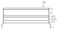
図4は、本発明の第4の実施形態に係るマスクブランク130の構成を示す断面図である。本実施形態におけるマスクブランク130では、位相シフト膜2は、透光性基板1側から、第1層21、第2層22、第3A層25が積層した構造を有する。第1層21、第2層22については、好適な屈折率や消衰係数、膜厚は、第1の実施形態において述べた通りであるので、説明を省略する。透光性基板1、遮光膜3、ハードマスク膜4の構成に関しても、第1の実施形態において述べた通りである。
FIG. 4 is a cross-sectional view showing the structure of a mask blank 130 according to a fourth embodiment of the invention. In the
第3A層25は、ケイ素と酸素とからなる材料、または半金属元素および非金属元素から選ばれる1以上の元素とケイ素と酸素とからなる材料で形成されることが好ましい。
第1層21の屈折率n1、第2層22の屈折率n2、第3A層25の屈折率n3Aは、n3A<n1<n2の関係を満たすことが好ましい。また、第1層21の消衰係数k1、第2層22の消衰係数k2、第3A層25の消衰係数k3Aは、k3A<k1<k2の関係を満たすことが好ましい。その上で、第3A層25の屈折率n3Aは、1.7以下であることが好ましく、1.65以下であるとより好ましい。また、第3A層25の屈折率n3Aは、1.50以上であることが好ましく、1.52以上であるとより好ましい。また、第3A層25の消衰係数k3Aは、0.02以下であることが好ましく、0.01以下であるとより好ましい。また、第3A層25の消衰係数k3Aは、0.00以上であることが好ましい。
The
The refractive index n 1 of the
第1層21の膜厚d1、第2層22の膜厚d2、第3A層25の膜厚d3Aは、d3A<d1<d2の関係を満たすことが好ましい。その上で、第3A層25の膜厚d3Aは30nm以下であると好ましく、25nm以下であるとより好ましい。また、第3A層25の膜厚d3Aは、2nm以上であることが好ましく、3nm以上であるとより好ましい。
第3A層25の酸素の含有量は、第1層21の酸素の含有量よりも多いことが好ましい。第3A層25の酸素の含有量は、50原子%以上であることが好ましく、55原子%以下であることがより好ましい。
The film thickness d 1 of the
The oxygen content of the
本実施形態におけるマスクブランク130は、上述のような構成とすることにより、略180度の位相差を生じさせることができるとともに、第1実施形態のマスクブランク100に比して、裏面反射率のさらなる低減が可能となる。 The mask blank 130 according to the present embodiment can generate a phase difference of approximately 180 degrees by being configured as described above, and the back surface reflectance is lower than that of the mask blank 100 according to the first embodiment. Further reduction is possible.
図5に、第1から第4の実施形態のマスクブランク100、110、120、130から製造される本発明の第1から第4の実施形態に係る位相シフトマスク200、210、220、230とその製造工程を示す。
図5(g)に示されているように、位相シフトマスク200、210、220、230は、マスクブランク100、110、120、130の位相シフト膜2に転写パターンである位相シフトパターン2aが形成され、遮光膜3に遮光パターン3bが形成されていることを特徴としている。マスクブランク100、110、120、130にハードマスク膜4が設けられている構成の場合、この位相シフトマスク200、210、220、230の作成途上でハードマスク膜4は除去される。
FIG. 5 shows phase shift masks 200, 210, 220 and 230 according to the first to fourth embodiments of the present invention manufactured from the
As shown in FIG. 5(g), the phase shift masks 200, 210, 220 and 230 have
本発明の第1から第4の実施形態に係る位相シフトマスク200、210、220、230の製造方法は、前記のマスクブランク100、110、120、130を用いるものであり、ドライエッチングにより遮光膜3に転写パターンを形成する工程と、転写パターンを有する遮光膜3をマスクとするドライエッチングにより位相シフト膜2に転写パターンを形成する工程と、遮光パターンを有するレジスト膜(第2のレジストパターン)6bをマスクとするドライエッチングにより遮光膜3に遮光パターン3bを形成する工程とを備えることを特徴としている。以下、図5に示す製造工程にしたがって、本発明の位相シフトマスク200、210、220、230の製造方法を説明する。なお、ここでは、遮光膜3の上にハードマスク膜4が積層したマスクブランク100、110、120、130を用いた位相シフトマスク200、210、220、230の製造方法について説明する。また、遮光膜3にはクロムを含有する材料を適用し、ハードマスク膜4にはケイ素を含有する材料を適用した場合について述べる。
The method of manufacturing the phase shift masks 200, 210, 220, and 230 according to the first to fourth embodiments of the present invention uses the
まず、マスクブランク100、110、120、130におけるハードマスク膜4に接して、レジスト膜をスピン塗布法によって形成する。次に、レジスト膜に対して、位相シフト膜2に形成すべき転写パターン(位相シフトパターン)である第1のパターンを電子線で露光描画し、さらに現像処理等の所定の処理を行い、位相シフトパターンを有する第1のレジストパターン5aを形成した(図5(a)参照)。続いて、第1のレジストパターン5aをマスクとして、フッ素系ガスを用いたドライエッチングを行い、ハードマスク膜4に第1のパターン(ハードマスクパターン4a)を形成した(図5(b)参照)。
First, a resist film is formed in contact with the
次に、レジストパターン5aを除去してから、ハードマスクパターン4aをマスクとして、塩素系ガスと酸素ガスの混合ガスを用いたドライエッチングを行い、遮光膜3に第1のパターン(遮光パターン3a)を形成する(図5(c)参照)。続いて、遮光パターン3aをマスクとして、フッ素系ガスを用いたドライエッチングを行い、位相シフト膜2に第1のパターン(位相シフトパターン2a)を形成し、かつハードマスクパターン4aを除去した(図5(d)参照)。
Next, after removing the resist
次に、マスクブランク100、110、120、130上にレジスト膜をスピン塗布法によって形成した。次に、レジスト膜に対して、遮光膜3に形成すべきパターン(遮光パターン)である第2のパターンを電子線で露光描画し、さらに現像処理等の所定の処理を行い、遮光パターンを有する第2のレジストパターン6bを形成した(図5(e)参照)。続いて、第2のレジストパターン6bをマスクとして、塩素系ガスと酸素ガスの混合ガスを用いたドライエッチングを行い、遮光膜3に第2のパターン(遮光パターン3b)を形成した(図5(f)参照)。さらに、第2のレジストパターン6bを除去し、洗浄等の所定の処理を経て、位相シフトマスク200、210、220、230を得た(図5(g)参照)。
Next, resist films were formed on the
前記のドライエッチングで使用される塩素系ガスとしては、Clが含まれていれば特に制限はない。たとえば、Cl2、SiCl2、CHCl3、CH2Cl2、CCl4、BCl3等があげられる。また、前記のドライエッチングで使用されるフッ素系ガスとしては、Fが含まれていれば特に制限はない。たとえば、CHF3、CF4、C2F6、C4F8、SF6等があげられる。特に、Cを含まないフッ素系ガスは、ガラス基板に対するエッチングレートが比較的低いため、ガラス基板へのダメージをより小さくすることができる。 The chlorine-based gas used in the dry etching is not particularly limited as long as it contains Cl. Examples include Cl 2 , SiCl 2 , CHCl 3 , CH 2 Cl 2 , CCl 4 , BCl 3 and the like. The fluorine-based gas used in the dry etching is not particularly limited as long as it contains F. Examples include CHF 3 , CF 4 , C 2 F 6 , C 4 F 8 , SF 6 and the like. In particular, a fluorine-based gas that does not contain C has a relatively low etching rate for a glass substrate, so damage to the glass substrate can be further reduced.
本発明の位相シフトマスク200、210、220、230は、前記のマスクブランク100、110、120、130を用いて作製されたものである。このため、転写パターンが形成された位相シフト膜2(位相シフトパターン2a)はArFエキシマレーザーの露光光に対する透過率が15%以上であり、かつ位相シフトパターン2aを透過した露光光と位相シフトパターン2aの厚さと同じ距離だけ空気中を通過した露光光との間における位相差が150度以上200度以下の範囲内となっている。また、この位相シフトマスク200は、遮光パターン3bが積層していない位相シフトパターン2aの領域(位相シフトパターン2aのみが存在する透光性基板1上の領域)における裏面反射率が9%以下になっている。これにより、位相シフトマスク200を用いて転写対象物(半導体ウェハ上のレジスト膜等)へ露光転写を行ったときに、上記の迷光によって露光転写像に与える影響を抑制することができる。
The phase shift masks 200, 210, 220, 230 of the present invention are produced using the
本発明の半導体デバイスの製造方法は、前記の位相シフトマスク200、210、220、230を用い、半導体基板上のレジスト膜に転写パターンを露光転写することを特徴としている。位相シフトマスク200、210、220、230は、ArFエキシマレーザーの露光光に対して所定の透過率で透過する機能とその透過するArFエキシマレーザーの露光光に対して所定の位相差を生じさせる機能を兼ね備え、裏面反射率が9%以下と従来のものに比して大幅に低減されている。このため、この位相シフトマスク200、210、220、230を露光装置にセットし、その位相シフトマスク200、210、220、230の透光性基板1側からArFエキシマレーザーの露光光を照射して転写対象物(半導体ウェハ上のレジスト膜等)へ露光転写する工程を行っても、位相シフトマスク200、210、220、230に形成されたバーコードやアライメントマークの転写対象物への映り込みを抑制できることができ、高い精度で転写対象物に所望のパターンを転写することができる。
The semiconductor device manufacturing method of the present invention is characterized by using the phase shift masks 200, 210, 220, and 230 and exposing and transferring a transfer pattern onto a resist film on a semiconductor substrate. The phase shift masks 200, 210, 220, and 230 have a function of transmitting the ArF excimer laser exposure light with a predetermined transmittance and a function of generating a predetermined phase difference with respect to the transmitted ArF excimer laser exposure light. , and the rear surface reflectance is 9% or less, which is greatly reduced compared to the conventional one. For this reason, the phase shift masks 200, 210, 220, and 230 are set in an exposure apparatus, and exposure light from an ArF excimer laser is irradiated from the
一方、上記の本発明の第1から第4の各実施形態で示した位相シフト膜の構成とは異なる、別の発明の位相シフト膜の構成であっても、ArFエキシマレーザーの露光光に対する所定の透過率と所定の位相差を兼ね備えつつ、9%以下の裏面反射率となる位相シフト膜を実現することは可能である。例えば、この別の発明のマスクブランクは、透光性基板上に、位相シフト膜を備えたマスクブランクであって、位相シフト膜は、透光性基板側から第1B層、第2B層、第3B層および第4B層の順に積層した構造を含み、第1B層は、前記透光性基板の表面に接して設けられ、第1B層、第2B層、第3B層および第4B層のArFエキシマレーザーの露光光の波長における屈折率をそれぞれn1B、n2B、n3B、n4Bとしたとき、n4B<n1B<n2Bおよびn4B<n3B<n2Bの関係を同時に満たし、第1B層、第2B層、第3B層および第4B層の露光光の波長における消衰係数をそれぞれk1B、k2B、k3B、k4Bとしたとき、k4B<k1B<k2Bおよびk4B<k3B<k2Bの関係を同時に満たし、第1B層、第2B層、第3B層および第4B層の膜厚をそれぞれd1B、d2B、d3B、d4Bとしたとき、d1B>d3B>d4Bおよびd2B>d3B>d4Bの関係を同時に満たすことを特徴とするマスクブランクがあげられる。なお、透光性基板、遮光膜、ハードマスク膜の構成に関しては、上記の第1の実施形態において述べたものと同様である。また、位相シフト膜に関しても、以降に記述する点以外については、上記の第1の実施形態において述べたものと同様である。 On the other hand, even in the configuration of the phase shift film of another invention, which is different from the configuration of the phase shift film shown in each of the first to fourth embodiments of the present invention, a predetermined It is possible to realize a phase shift film having a rear surface reflectance of 9% or less while having both a transmittance of 1 and a predetermined phase difference. For example, the mask blank of this another invention is a mask blank having a phase shift film on a translucent substrate, wherein the phase shift film is composed of a first B layer, a second B layer and a second B layer from the translucent substrate side. It includes a structure in which a 3B layer and a 4th B layer are laminated in order, the 1B layer being provided in contact with the surface of the translucent substrate, and the ArF excimers of the 1B layer, the 2B layer, the 3B layer and the 4B layer. Let n 1B , n 2B , n 3B , and n 4B be the refractive indices at the wavelengths of the exposure light of the laser, respectively . When the extinction coefficients of the 1B layer, the 2B layer, the 3B layer and the 4B layer at the wavelength of the exposure light are respectively k 1B , k 2B , k 3B and k 4B , k 4B < k 1B < k 2B and k When the relationship 4B < k 3B < k 2B is simultaneously satisfied, and the film thicknesses of the 1B layer, the 2B layer, the 3B layer, and the 4B layer are d 1B , d 2B , d 3B , and d 4B , respectively, d 1B >d 3B >d 4B and d 2B >d 3B >d 4B at the same time. The configurations of the translucent substrate, the light shielding film, and the hard mask film are the same as those described in the first embodiment. Also, the phase shift film is the same as that described in the above-described first embodiment, except for the points described below.
第1B層および第3B層は、ケイ素と窒素と酸素とからなる材料、または半金属元素および非金属元素から選ばれる1以上の元素とケイ素と窒素と酸素とからなる材料で形成されることが好ましい。また、第2B層は、ケイ素と窒素とからなる材料、または半金属元素および非金属元素から選ばれる1以上の元素とケイ素と窒素とからなる材料で形成されることが好ましい。第4B層は、ケイ素と酸素とからなる材料、または半金属元素および非金属元素から選ばれる1以上の元素とケイ素と酸素とからなる材料で形成されることが好ましい。 The 1B layer and the 3B layer can be formed of a material consisting of silicon, nitrogen, and oxygen, or a material consisting of one or more elements selected from metalloid elements and nonmetallic elements and silicon, nitrogen, and oxygen. preferable. Also, the second layer B is preferably formed of a material consisting of silicon and nitrogen, or a material consisting of one or more elements selected from metalloid elements and nonmetallic elements, silicon, and nitrogen. The fourth B layer is preferably made of a material consisting of silicon and oxygen, or a material consisting of one or more elements selected from metalloid elements and nonmetallic elements, silicon and oxygen.
第1B層の屈折率n1Bは、1.8以上であると好ましく、1.85以上であるとより好ましい。また、第1B層の屈折率n1Bは、2.2未満であると好ましく、2.15以下であるとより好ましい。第1B層の消衰係数k1Bは、0.15以下であることが好ましく、0.14以下であるとより好ましい。また、第1B層の消衰係数k1Bは、0.05以上であると好ましく、0.06以上であるとより好ましい。第1B層の膜厚d1Bは、35nm以下であると好ましく、33nm以下であるとより好ましい。また、第1B層の膜厚d1Bは、20nmより大きいことが好ましく、21nm以上であるとより好ましい。 The refractive index n1B of the 1B layer is preferably 1.8 or more, more preferably 1.85 or more. Further, the refractive index n1B of the 1B layer is preferably less than 2.2, more preferably 2.15 or less. The extinction coefficient k1B of the 1B layer is preferably 0.15 or less, more preferably 0.14 or less. The extinction coefficient k1B of the 1B layer is preferably 0.05 or more, more preferably 0.06 or more. The film thickness d1B of the 1B layer is preferably 35 nm or less, more preferably 33 nm or less. Also, the film thickness d1B of the 1B layer is preferably larger than 20 nm, more preferably 21 nm or more.
第2B層の屈折率n2Bは、2.2以上であることが好ましく、2.25以上であるとより好ましい。また、第2B層の屈折率n2Bは、3.0以下であると好ましく、2.8以下であるとより好ましい。また、第2B層の消衰係数k2Bは、0.2以上であることが好ましく、0.25以上であるとより好ましい。また、第2B層の消衰係数k2Bは、0.5以下であると好ましく、0.4以下であるとより好ましい。第2B層の膜厚d2Bは、35nm以下であると好ましく、33nm以下であるとより好ましい。また、第2B層の膜厚d2Bは、20nmより大きいことが好ましく、21nm以上であるとより好ましい。 The refractive index n2B of the layer 2B is preferably 2.2 or more, more preferably 2.25 or more. Further, the refractive index n2B of the second B layer is preferably 3.0 or less, more preferably 2.8 or less. The extinction coefficient k2B of the second B layer is preferably 0.2 or more, more preferably 0.25 or more. The extinction coefficient k2B of the second B layer is preferably 0.5 or less, more preferably 0.4 or less. The film thickness d2B of the second B layer is preferably 35 nm or less, more preferably 33 nm or less. Also, the film thickness d2B of the second B layer is preferably larger than 20 nm, more preferably 21 nm or more.
第3B層の屈折率n3Bは、1.8以上であると好ましく、1.85以上であるとより好ましい。また、第3B層の屈折率n3Bは、2.2未満であると好ましく、2.15以下であるとより好ましい。第3B層の消衰係数k3Bは、0.15以下であることが好ましく、0.14以下であるとより好ましい。また、第3B層の消衰係数k3Bは、0.05以上であると好ましく、0.06以上であるとより好ましい。第3B層の膜厚d3Bは、20nm以下であると好ましく、19nm以下であるとより好ましい。また、第3B層の膜厚d3Bは、10nm以上であることが好ましく、15nm以上であるとより好ましい。 The refractive index n3B of the 3B layer is preferably 1.8 or more, more preferably 1.85 or more. Further, the refractive index n3B of the 3B layer is preferably less than 2.2, more preferably 2.15 or less. The extinction coefficient k3B of the 3B layer is preferably 0.15 or less, more preferably 0.14 or less. The extinction coefficient k3B of the 3B layer is preferably 0.05 or more, more preferably 0.06 or more. The film thickness d3B of the 3B layer is preferably 20 nm or less, more preferably 19 nm or less. The film thickness d3B of the 3B layer is preferably 10 nm or more, more preferably 15 nm or more.
第4B層の屈折率n4Bは、1.7以下であることが好ましく、1.65以下であるとより好ましい。また、第4B層の屈折率n4Bは、1.50以上であることが好ましく、1.52以上であるとより好ましい。また、第4B層の消衰係数k4Bは、0.1以下であることが好ましく、0.01以下であるとより好ましい。また、第4B層の消衰係数k4Bは、0.00以上であることが好ましい。第4B層の膜厚d4Bは、10nmよりも小さいことが好ましく、9nm以下であるとより好ましい。また、第4B層の膜厚d4Bは、2nm以上であることが好ましく、3nm以上であるとより好ましい。 The refractive index n4B of the fourth B layer is preferably 1.7 or less, more preferably 1.65 or less. The refractive index n4B of the 4B layer is preferably 1.50 or more, more preferably 1.52 or more. The extinction coefficient k4B of the 4B layer is preferably 0.1 or less, more preferably 0.01 or less. Further, the extinction coefficient k4B of the 4B layer is preferably 0.00 or more. The film thickness d4B of the fourth B layer is preferably less than 10 nm, more preferably 9 nm or less. The film thickness d4B of the fourth B layer is preferably 2 nm or more, more preferably 3 nm or more.
第2B層の窒素の含有量は、第1B層および第3B層の窒素の含有量よりも多いことが好ましい。第1B層および第3B層の窒素の含有量は、40原子%以下であることが好ましく、30原子%以下であることがより好ましい。また、第1B層および第3B層の窒素の含有量は、10原子%以上であることが好ましく、15原子%以上であることがより好ましい。一方、第2B層の窒素の含有量は、45原子%以上であることが好ましく、50原子%以上であることがより好ましく、55原子%以上であることがさらに好ましい。第2層Bは、屈折率が高い材料で形成されることが好ましいが、窒素含有量を多くすることで屈折率を高くすることができるためである。 The nitrogen content of the 2B layer is preferably higher than the nitrogen content of the 1B layer and the 3B layer. The nitrogen content of the 1B layer and the 3B layer is preferably 40 atomic % or less, more preferably 30 atomic % or less. Further, the nitrogen content in the 1B layer and the 3B layer is preferably 10 atomic % or more, more preferably 15 atomic % or more. On the other hand, the nitrogen content of the layer 2B is preferably 45 atomic % or more, more preferably 50 atomic % or more, and even more preferably 55 atomic % or more. The second layer B is preferably made of a material with a high refractive index, because the refractive index can be increased by increasing the nitrogen content.
第1B層および第3B層の酸素の含有量は、第2B層の酸素の含有量よりも多いことが好ましい。第1B層および第3B層の酸素の含有量は、10原子%以上であることが好ましく、15原子%以上であることがより好ましい。また、第1B層および第3B層の酸素の含有量は、45原子%以下であることが好ましく、40原子%以下であることがより好ましい。一方、第2B層の酸素の含有量は、5原子%以下であることが好ましく、2原子%以下であることがより好ましい。第2B層は、酸素を含有しないことがさらに好ましい。第2B層の酸素の含有量が増えるにつれて第2層22の屈折率が低下するためである。
The oxygen content of the 1B layer and the 3B layer is preferably higher than the oxygen content of the 2B layer. The oxygen content of the 1B layer and the 3B layer is preferably 10 atomic % or more, more preferably 15 atomic % or more. Further, the oxygen content of the 1B layer and the 3B layer is preferably 45 atomic % or less, more preferably 40 atomic % or less. On the other hand, the oxygen content of the layer 2B is preferably 5 atomic % or less, more preferably 2 atomic % or less. More preferably, the second B layer does not contain oxygen. This is because the refractive index of the
第4B層の酸素の含有量は、第1B層、第2B層および第3B層の酸素の含有量よりも多いことが好ましい。第4B層の酸素の含有量は、50原子%以上であることが好ましく、55原子%以下であることがより好ましい。 The oxygen content of the 4th B layer is preferably higher than the oxygen content of the 1st B layer, the 2nd B layer and the 3rd B layer. The oxygen content of the 4th B layer is preferably 50 atomic % or more, and more preferably 55 atomic % or less.
一方、上記の第1から第4の実施形態のマスクブランクから位相シフトマスクを製造する場合と同様の手順で、この別の発明のマスクブランクから位相シフトマスクを製造することができる。この別の発明の位相シフトマスクは、上記の別の発明のマスクブランクの位相シフト膜に転写パターンである位相シフトパターンが形成され、遮光膜に遮光パターンが形成されていることを特徴としている。 On the other hand, a phase shift mask can be manufactured from the mask blank of this other invention in the same procedure as in the case of manufacturing the phase shift mask from the mask blanks of the first to fourth embodiments. The phase shift mask of this another invention is characterized in that a phase shift pattern, which is a transfer pattern, is formed on the phase shift film of the mask blank of the above another invention, and a light shielding pattern is formed on the light shielding film.
一方、上記の本発明の半導体デバイスの製造方法についても、上記の別の発明の位相シフトマスクを用いることが可能である。この別の発明の位相シフトマスクも、ArFエキシマレーザーの露光光に対して所定の透過率で透過する機能とその透過するArFエキシマレーザーの露光光に対して所定の位相差を生じさせる機能を兼ね備え、裏面反射率が9%以下と従来のものに比して大幅に低減されている。このため、この別の発明の位相シフトマスクを露光装置にセットし、その別の発明の位相シフトマスクの透光性基板側からArFエキシマレーザーの露光光を照射して転写対象物(半導体ウェハ上のレジスト膜等)へ露光転写する工程を行っても、その別の発明の位相シフトマスクに形成されたバーコードやアライメントマークの転写対象物への映り込みを抑制できることができ、高い精度で転写対象物に所望のパターンを転写することができる。 On the other hand, it is also possible to use the phase shift mask of another aspect of the invention in the method of manufacturing a semiconductor device of the aspect of the invention. The phase shift mask of this other invention also has the function of transmitting the ArF excimer laser exposure light with a predetermined transmittance and the function of generating a predetermined phase difference with respect to the transmitted ArF excimer laser exposure light. , the back surface reflectance is 9% or less, which is greatly reduced compared to the conventional one. For this reason, the phase shift mask of this another invention is set in an exposure apparatus, and the exposure light of an ArF excimer laser is irradiated from the transparent substrate side of the phase shift mask of this another invention to transfer an object (on a semiconductor wafer). (Resist film, etc.), it is possible to suppress reflection of the bar code or alignment mark formed on the phase shift mask of the other invention on the transfer target, and transfer with high accuracy. A desired pattern can be transferred to the object.
以下、実施例により、本発明の実施の形態をさらに具体的に説明する。
(実施例1)
[マスクブランクの製造]
主表面の寸法が約152mm×約152mmで、厚さが約6.35mmの合成石英ガラスからなる透光性基板1を準備した。この透光性基板1は、端面及び主表面を所定の表面粗さに研磨され、その後、所定の洗浄処理および乾燥処理を施されたものである。この透光性基板1の光学特性を測定したところ、屈折率nSが1.556、消衰係数kSが0.00であった。
EXAMPLES The embodiments of the present invention will be described in more detail below with reference to examples.
(Example 1)
[Manufacturing of mask blank]
A
次に、枚葉式RFスパッタ装置内に透光性基板1を設置し、ケイ素(Si)ターゲットを用い、アルゴン(Ar)ガス、酸素(O2)および窒素(N2)の混合ガスをスパッタリングガスとするRFスパッタリングにより、透光性基板1の表面に接してケイ素、酸素および窒素からなる位相シフト膜2の第1層21(SiON膜 Si:O:N=40原子%:35原子%:25原子%)を29.5nmの厚さで形成した。続いて、ケイ素(Si)ターゲットを用い、アルゴン(Ar)および窒素(N2)の混合ガスをスパッタリングガスとする反応性スパッタリング(RFスパッタリング)により、第1層21上に、ケイ素および窒素からなる位相シフト膜2の第2層22(SiN膜 Si:N=43原子%:57原子%)を41.5nmの厚さで形成した。以上の手順により、透光性基板1の表面に接して第1層21、第2層22が積層した位相シフト膜2を71nmの厚さで形成した。なお、第1層21、第2層22の組成は、X線光電子分光法(XPS)による測定によって得られた結果である。以下、他の膜に関しても同様である。
Next, the
次に、位相シフト量測定装置(レーザーテック社製 MPM193)を用いて、その位相シフト膜2の波長193nmの光に対する透過率と位相差を測定したところ、透過率が27.4%、位相差が183.2度(deg)であった。さらに、この位相シフト膜2の第1層21、第2層22の各光学特性を分光エリプソメーター(J.A.Woollam社製 M-2000D)で測定したところ、第1層21は屈折率n1が1.990、消衰係数k1が0.085であり、第2層22は、屈折率n2が2.595、消衰係数k2が0.357であった。ArFエキシマレーザーの露光光の波長の光に対する位相シフト膜2の裏面反射率は3.7%であり、9%を下回るものであった。
Next, when the transmittance and phase difference of the
次に、枚葉式DCスパッタ装置内に位相シフト膜2が形成された透光性基板1を設置し、クロム(Cr)ターゲットを用い、アルゴン(Ar)、二酸化炭素(CO2)、窒素(N2)およびヘリウム(He)の混合ガスをスパッタリングガスとする反応性スパッタリング(DCスパッタリング)により、位相シフト膜2上にCrOCNからなる遮光膜3(CrOCN膜 Cr:O:C:N=55原子%:22原子%:12原子%:11原子%)を59.5nmの厚さで形成した。この透光性基板1上に位相シフト膜2と遮光膜3が積層した状態におけるArFエキシマレーザーの露光光の波長の光に対する裏面反射率は0.5%であり、9%を下回るものであった。この位相シフト膜2と遮光膜3の積層構造における波長193nmの光に対する光学濃度(OD)を測定したところ、3.0以上であった。また、別の透光性基板1を準備し、同じ成膜条件で遮光膜3のみを成膜し、その遮光膜3の光学特性を上記分光エリプソメーターで測定したところ、屈折率nが1.92、消衰係数kが1.50であった。
Next, the
次に、枚葉式RFスパッタ装置内に、位相シフト膜2および遮光膜3が積層された透光性基板1を設置し、二酸化ケイ素(SiO2)ターゲットを用い、アルゴン(Ar)ガスをスパッタリングガスとし、RFスパッタリングにより遮光膜3の上に、ケイ素および酸素からなるハードマスク膜4を5nmの厚さで形成した。以上の手順により、透光性基板1上に、3層構造の位相シフト膜2、遮光膜3およびハードマスク膜4が積層した構造を備えるマスクブランク100を製造した。
Next, the light-transmitting
[位相シフトマスクの製造]
次に、この実施例1のマスクブランク100を用い、以下の手順で実施例1の位相シフトマスク200を作製した。最初に、ハードマスク膜4の表面にHMDS処理を施した。続いて、スピン塗布法によって、ハードマスク膜4の表面に接して、電子線描画用化学増幅型レジストからなるレジスト膜を膜厚80nmで形成した。次に、このレジスト膜に対して、位相シフト膜2に形成すべき位相シフトパターンである第1のパターンを電子線描画し、所定の現像処理および洗浄処理を行い、第1のパターンを有する第1のレジストパターン5aを形成した(図5(a)参照)。このとき、第1のレジストパターン5aには、パターン形成領域外において、バーコードやアライメントマークに対応する形状のパターンも併せて形成した。
[Manufacture of phase shift mask]
Next, using the
次に、第1のレジストパターン5aをマスクとし、CF4ガスを用いたドライエッチングを行い、ハードマスク膜4に第1のパターン(ハードマスクパターン4a)を形成した(図5(b)参照)。このとき、ハードマスク膜4には、パターン形成領域外において、バーコードやアライメントマークに対応する形状のパターンも併せて形成した。その後、第1のレジストパターン5aを除去した。
Next, using the first resist
続いて、ハードマスクパターン4aをマスクとし、塩素と酸素の混合ガス(ガス流量比 Cl2:O2=10:1)を用いたドライエッチングを行い、遮光膜3に第1のパターン(遮光パターン3a)を形成した(図5(c)参照)。このとき、遮光膜3には、パターン形成領域外において、バーコードやアライメントマークに対応する形状のパターンも併せて形成した。次に、遮光パターン3aをマスクとし、フッ素系ガス(SF6+He)を用いたドライエッチングを行い、位相シフト膜2に第1のパターン(位相シフトパターン2a)を形成し、かつ同時にハードマスクパターン4aを除去した(図5(d)参照)。このとき、位相シフト膜2には、パターン形成領域外において、バーコードやアライメントマークに対応する形状のパターンも併せて形成した。
Subsequently, using the
次に、遮光パターン3a上に、スピン塗布法によって、電子線描画用化学増幅型レジストからなるレジスト膜を膜厚150nmで形成した。次に、レジスト膜に対して、遮光膜に形成すべきパターン(遮光パターン)である第2のパターンを露光描画し、さらに現像処理等の所定の処理を行い、遮光パターンを有する第2のレジストパターン6bを形成した(図5(e)参照)。続いて、第2のレジストパターン6bをマスクとして、塩素と酸素の混合ガス(ガス流量比 Cl2:O2=4:1)を用いたドライエッチングを行い、遮光膜3に第2のパターン(遮光パターン3b)を形成した(図5(f)参照)。さらに、第2のレジストパターン6bを除去し、洗浄等の所定の処理を経て、位相シフトマスク200を得た(図5(g)参照)。
Next, a resist film made of a chemically amplified resist for electron beam drawing was formed on the
この位相シフトマスク200に対し、AIMS193(Carl Zeiss社製)を用いて、ArFエキシマレーザーの露光光で半導体デバイス上のレジスト膜に露光転写したときにおける露光転写像のシミュレーションを行った。このシミュレーションで得られた露光転写像を検証したところ、設計仕様を十分に満たしていた。また、露光転写像には、バーコードやアライメントマークの映り込みに起因するCDばらつきは見られなかった。以上のことから、この実施例1のマスクブランクから製造された位相シフトマスク200は、露光装置にセットしてArFエキシマレーザーの露光光による露光転写を行っても、半導体デバイス上のレジスト膜に対して高精度で露光転写を行うことができるといえる。 Using AIMS193 (manufactured by Carl Zeiss), a simulation was performed on the phase shift mask 200 of the exposure transfer image when the resist film on the semiconductor device was exposed and transferred to the resist film on the semiconductor device with the exposure light of the ArF excimer laser. When the exposure transfer image obtained by this simulation was verified, it sufficiently satisfied the design specifications. In addition, no CD variation due to reflection of barcodes or alignment marks was observed in the exposure transfer image. From the above, even if the phase shift mask 200 manufactured from the mask blank of this Example 1 is set in an exposure apparatus and subjected to exposure transfer using exposure light of an ArF excimer laser, the resist film on the semiconductor device is not affected. It can be said that exposure transfer can be performed with high precision.
(実施例2)
[マスクブランクの製造]
実施例2のマスクブランク110は、位相シフト膜2以外については、実施例1と同様の手順で製造した。この実施例2の位相シフト膜2は、第2層22の上に第3層23を形成している。具体的には、枚葉式RFスパッタ装置内に透光性基板1を設置し、ケイ素(Si)ターゲットを用い、アルゴン(Ar)ガス、酸素(O2)および窒素(N2)の混合ガスをスパッタリングガスとするRFスパッタリングにより、透光性基板1の表面に接してケイ素、酸素および窒素からなる位相シフト膜2の第1層21(SiON膜 Si:O:N=40原子%:35原子%:25原子%)を29.5nmの厚さで形成した。続いて、ケイ素(Si)ターゲットを用い、アルゴン(Ar)および窒素(N2)の混合ガスをスパッタリングガスとする反応性スパッタリング(RFスパッタリング)により、第1層21上に、ケイ素および窒素からなる位相シフト膜2の第2層22(SiN膜 Si:N=43原子%:57原子%)を41.5nmの厚さで形成した。続いて、ケイ素(Si)ターゲットを用い、アルゴン(Ar)および窒素(N2)の混合ガスをスパッタリングガスとする反応性スパッタリング(RFスパッタリング)により、第2層22上に、ケイ素および窒素からなる位相シフト膜2の第3層23(Si:N=68原子%:32原子%)を3nmの厚さで形成した。以上の手順により、透光性基板1の表面に接して第1層21、第2層22、第3層23が積層した位相シフト膜2を74nmの厚さで形成した。
(Example 2)
[Manufacturing of mask blank]
The
上記位相シフト量測定装置を用いて、その位相シフト膜2のArFエキシマレーザーの露光光の波長(波長193nm)の光に対する透過率と位相差を測定したところ、透過率が19.6%、位相差が175.8度(deg)であった。さらに、この位相シフト膜2の第1層21、第2層22、第3層23の各光学特性を上記分光エリプソメーターで測定したところ、第1層21は屈折率n1が1.990、消衰係数k1が0.085であり、第2層22は、屈折率n2が2.595、消衰係数k2が0.357であり、第3層23は、屈折率n3が1.648、消衰係数k3が1.861であった。位相シフト膜2のArFエキシマレーザーの露光光の波長の光に対する裏面反射率(透光性基板1側の反射率)は6.3%であり、9%を下回るものであった。
Using the phase shift amount measuring device, the transmittance and phase difference of the
以上の手順により、透光性基板1上に、第1層21、第2層22、第3層23とからなる位相シフト膜2、遮光膜3およびハードマスク膜4が積層した構造を備える実施例2のマスクブランク110を製造した。なお、この実施例2のマスクブランク110は、透光性基板1上に位相シフト膜2と遮光膜3が積層した状態におけるArFエキシマレーザーの露光光の波長の光に対する裏面反射率(透光性基板1側の反射率)は6.9%であり、9%を下回るものであった。この位相シフト膜2と遮光膜3の積層構造における波長193nmの光に対する光学濃度(OD)を測定したところ、3.0以上であった。
By the above procedure, a structure in which the
[位相シフトマスクの製造]
次に、この実施例2のマスクブランク110を用い、実施例1と同様の手順で、実施例2の位相シフトマスク210を作製した。
[Manufacture of phase shift mask]
Next, using the
この位相シフトマスク210に対し、AIMS193(Carl Zeiss社製)を用いて、ArFエキシマレーザーの露光光で半導体デバイス上のレジスト膜に露光転写したときにおける露光転写像のシミュレーションを行った。このシミュレーションで得られた露光転写像を検証したところ、設計仕様を十分に満たしていた。また、露光転写像には、バーコードやアライメントマークの映り込みに起因するCDばらつきは見られなかった。以上のことから、この実施例2のマスクブランクから製造された位相シフトマスク210は、露光装置にセットしてArFエキシマレーザーの露光光による露光転写を行っても、半導体デバイス上のレジスト膜に対して高精度で露光転写を行うことができるといえる。 Using AIMS193 (manufactured by Carl Zeiss), a simulation was performed on the phase shift mask 210 by exposing and transferring the resist film on the semiconductor device with exposure light from an ArF excimer laser. When the exposure transfer image obtained by this simulation was verified, it sufficiently satisfied the design specifications. In addition, no CD variation due to reflection of barcodes or alignment marks was observed in the exposure transfer image. From the above, even if the phase shift mask 210 manufactured from the mask blank of this Example 2 is set in an exposure apparatus and subjected to exposure transfer with exposure light of an ArF excimer laser, the resist film on the semiconductor device is not affected. It can be said that exposure transfer can be performed with high precision.
(実施例3)
[マスクブランクの製造]
実施例3のマスクブランク120は、位相シフト膜2以外については、実施例1と同様の手順で製造した。この実施例3の位相シフト膜2は、第3層23の上に第4層24を形成している。具体的には、枚葉式RFスパッタ装置内に透光性基板1を設置し、ケイ素(Si)ターゲットを用い、アルゴン(Ar)ガス、酸素(O2)および窒素(N2)の混合ガスをスパッタリングガスとするRFスパッタリングにより、透光性基板1の表面に接してケイ素、酸素および窒素からなる位相シフト膜2の第1層21(SiON膜 Si:O:N=40原子%:35原子%:25原子%)を29.5nmの厚さで形成した。続いて、ケイ素(Si)ターゲットを用い、アルゴン(Ar)および窒素(N2)の混合ガスをスパッタリングガスとする反応性スパッタリング(RFスパッタリング)により、第1層21上に、ケイ素および窒素からなる位相シフト膜2の第2層22(SiN膜 Si:N=43原子%:57原子%)を41.5nmの厚さで形成した。続いて、ケイ素(Si)ターゲットを用い、アルゴン(Ar)および窒素(N2)の混合ガスをスパッタリングガスとする反応性スパッタリング(RFスパッタリング)により、第2層22上に、ケイ素および窒素からなる位相シフト膜2の第3層23(Si:N=68原子%:32原子%)を3nmの厚さで形成した。続いて、ケイ素(Si)ターゲットを用い、アルゴン(Ar)および酸素(O2)の混合ガスをスパッタリングガスとする反応性スパッタリング(RFスパッタリング)により、第3層23上に、ケイ素および酸素からなる位相シフト膜2の第4層24(SiO膜 Si:O=33原子%:67原子%)を3nmの厚さで形成した。以上の手順により、透光性基板1の表面に接して第1層21、第2層22、第3層23、第4層24が積層した位相シフト膜2を77nmの厚さで形成した。
(Example 3)
[Manufacturing of mask blank]
A
上記位相シフト量測定装置を用いて、その位相シフト膜2のArFエキシマレーザーの露光光の波長(波長193nm)の光に対する透過率と位相差を測定したところ、透過率が20.1%、位相差が178.0度(deg)であった。さらに、この位相シフト膜2の第1層21、第2層22、第3層23、第4層24の各光学特性を上記分光エリプソメーターで測定したところ、第1層21は屈折率n1が1.990、消衰係数k1が0.085であり、第2層22は、屈折率n2が2.595、消衰係数k2が0.357であり、第3層23は、屈折率n3が1.648、消衰係数k3が1.861であり、第4層24は、屈折率n4が1.590、消衰係数k4が0.000であった。位相シフト膜2のArFエキシマレーザーの露光光の波長の光に対する裏面反射率(透光性基板1側の反射率)は5.8%であり、9%を下回るものであった。
Using the phase shift amount measuring device, the transmittance and phase difference of the
以上の手順により、透光性基板1上に、第1層21、第2層22、第3層23、第4層24とからなる位相シフト膜2、遮光膜3およびハードマスク膜4が積層した構造を備える実施例3のマスクブランク120を製造した。なお、この実施例3のマスクブランク120は、透光性基板1上に位相シフト膜2と遮光膜3が積層した状態における波長193nmの光に対する裏面反射率(透光性基板1側の反射率)は7.7%であり、9%を下回るものであった。この位相シフト膜2と遮光膜3の積層構造における波長193nmの光に対する光学濃度(OD)を測定したところ、3.0以上であった。
By the above procedure, the
[位相シフトマスクの製造]
次に、この実施例3のマスクブランク120を用い、実施例1と同様の手順で、実施例3の位相シフトマスク220を作製した。
[Manufacture of phase shift mask]
Next, using the
この位相シフトマスク220に対し、AIMS193(Carl Zeiss社製)を用いて、ArFエキシマレーザーの露光光で半導体デバイス上のレジスト膜に露光転写したときにおける露光転写像のシミュレーションを行った。このシミュレーションで得られた露光転写像を検証したところ、設計仕様を十分に満たしていた。また、露光転写像には、バーコードやアライメントマークの映り込みに起因するCDばらつきは見られなかった。以上のことから、この実施例3のマスクブランクから製造された位相シフトマスク220は、露光装置にセットしてArFエキシマレーザーの露光光による露光転写を行っても、半導体デバイス上のレジスト膜に対して高精度で露光転写を行うことができるといえる。 Using AIMS193 (manufactured by Carl Zeiss), a simulation of the exposure transfer image when the phase shift mask 220 is exposed and transferred to the resist film on the semiconductor device with the exposure light of the ArF excimer laser was performed. When the exposure transfer image obtained by this simulation was verified, it sufficiently satisfied the design specifications. In addition, no CD variation due to reflection of barcodes or alignment marks was observed in the exposure transfer image. From the above, even if the phase shift mask 220 manufactured from the mask blank of this Example 3 is set in an exposure apparatus and subjected to exposure transfer using exposure light of an ArF excimer laser, the resist film on the semiconductor device is not affected. It can be said that exposure transfer can be performed with high precision.
(実施例4)
[マスクブランクの製造]
実施例4のマスクブランク130は、位相シフト膜2以外については、実施例1と同様の手順で製造した。この実施例4の位相シフト膜2は、第2層22の上に、第3層23と組成の異なる第3A層25を形成している。具体的には、枚葉式RFスパッタ装置内に透光性基板1を設置し、ケイ素(Si)ターゲットを用い、アルゴン(Ar)ガス、酸素(O2)および窒素(N2)の混合ガスをスパッタリングガスとするRFスパッタリングにより、透光性基板1の表面に接してケイ素、酸素および窒素からなる位相シフト膜2の第1層21(SiON膜 Si:O:N=40原子%:35原子%:25原子%)を29.5nmの厚さで形成した。続いて、ケイ素(Si)ターゲットを用い、アルゴン(Ar)および窒素(N2)の混合ガスをスパッタリングガスとする反応性スパッタリング(RFスパッタリング)により、第1層21上に、ケイ素および窒素からなる位相シフト膜2の第2層22(SiN膜 Si:N=43原子%:57原子%)を41.5nmの厚さで形成した。続いて、ケイ素(Si)ターゲットを用い、アルゴン(Ar)および酸素(O2)の混合ガスをスパッタリングガスとする反応性スパッタリング(RFスパッタリング)により、第2層22上に、ケイ素および酸素からなる位相シフト膜2の第3A層25(SiO膜 Si:O=33原子%:67原子%)を3nmの厚さで形成した。以上の手順により、透光性基板1の表面に接して第1層21、第2層22、第3A層25が積層した位相シフト膜2を74nmの厚さで形成した。
(Example 4)
[Manufacturing of mask blank]
A
上記位相シフト量測定装置を用いて、その位相シフト膜2のArFエキシマレーザーの露光光の波長(波長193nm)の光に対する透過率と位相差を測定したところ、透過率が27.7%、位相差が179.3度(deg)であった。さらに、この位相シフト膜2の第1層21、第2層22、第3A層25の各光学特性を上記分光エリプソメーターで測定したところ、第1層21は屈折率n1が1.990、消衰係数k1が0.085であり、第2層22は、屈折率n2が2.595、消衰係数k2が0.357であり、第3A層25は、屈折率n3Aが1.590、消衰係数k3Aが0.000であった。位相シフト膜2のArFエキシマレーザーの露光光の波長の光に対する裏面反射率(透光性基板1側の反射率)は8.4%であり、9%を下回るものであった。
Using the phase shift amount measuring device, the transmittance and phase difference of the
以上の手順により、透光性基板1上に、第1層21、第2層22、第3A層25とからなる位相シフト膜2、遮光膜3およびハードマスク膜4が積層した構造を備える実施例4のマスクブランク130を製造した。なお、この実施例4のマスクブランク130は、透光性基板1上に位相シフト膜2と遮光膜3が積層した状態におけるArFエキシマレーザーの露光光の波長の光に対する裏面反射率(透光性基板1側の反射率)は8.3%であり、9%を下回るものであった。この位相シフト膜2と遮光膜3の積層構造における波長193nmの光に対する光学濃度(OD)を測定したところ、3.0以上であった。
By the above procedure, the structure in which the
[位相シフトマスクの製造]
次に、この実施例4のマスクブランク130を用い、実施例1と同様の手順で、実施例4の位相シフトマスク230を作製した。
[Manufacture of phase shift mask]
Next, using the
この位相シフトマスク230に対し、AIMS193(Carl Zeiss社製)を用いて、ArFエキシマレーザーの露光光で半導体デバイス上のレジスト膜に露光転写したときにおける露光転写像のシミュレーションを行った。このシミュレーションで得られた露光転写像を検証したところ、設計仕様を十分に満たしていた。また、露光転写像には、バーコードやアライメントマークの映り込みに起因するCDばらつきは見られなかった。以上のことから、この実施例4のマスクブランクから製造された位相シフトマスク230は、露光装置にセットしてArFエキシマレーザーの露光光による露光転写を行っても、半導体デバイス上のレジスト膜に対して高精度で露光転写を行うことができるといえる。 Using AIMS193 (manufactured by Carl Zeiss), a simulation was performed on the phase shift mask 230 by exposing and transferring the resist film on the semiconductor device with exposure light from an ArF excimer laser. When the exposure transfer image obtained by this simulation was verified, it sufficiently satisfied the design specifications. In addition, no CD variation due to reflection of barcodes or alignment marks was observed in the exposure transfer image. From the above, even if the phase shift mask 230 manufactured from the mask blank of this Example 4 is set in an exposure apparatus and subjected to exposure transfer using the exposure light of the ArF excimer laser, the resist film on the semiconductor device is not affected. It can be said that exposure transfer can be performed with high precision.
(実施例5)
[マスクブランクの製造]
実施例5のマスクブランク130は、位相シフト膜2以外については、実施例1と同様の手順で製造した。この実施例5の位相シフト膜2は、第1層21、第2層22、第3A層25のそれぞれの膜厚を実施例4のものから変更している。具体的には、枚葉式RFスパッタ装置内に透光性基板1を設置し、ケイ素(Si)ターゲットを用い、アルゴン(Ar)ガス、酸素(O2)および窒素(N2)の混合ガスをスパッタリングガスとするRFスパッタリングにより、透光性基板1の表面に接してケイ素、酸素および窒素からなる位相シフト膜2の第1層21(SiON膜 Si:O:N=40原子%:35原子%:25原子%)を31nmの厚さで形成した。続いて、ケイ素(Si)ターゲットを用い、アルゴン(Ar)および窒素(N2)の混合ガスをスパッタリングガスとする反応性スパッタリング(RFスパッタリング)により、第1層21上に、ケイ素および窒素からなる位相シフト膜2の第2層22(SiN膜 Si:N=43原子%:57原子%)を38nmの厚さで形成した。続いて、ケイ素(Si)ターゲットを用い、アルゴン(Ar)および酸素(O2)の混合ガスをスパッタリングガスとする反応性スパッタリング(RFスパッタリング)により、第2層22上に、ケイ素および酸素からなる位相シフト膜2の第3A層25(SiO膜 Si:O=33原子%:67原子%)を20nmの厚さで形成した。以上の手順により、透光性基板1の表面に接して第1層21、第2層22、第3A層25が積層した位相シフト膜2を89nmの厚さで形成した。
(Example 5)
[Manufacturing of mask blank]
A
上記位相シフト量測定装置を用いて、その位相シフト膜2のArFエキシマレーザーの露光光の波長(波長193nm)の光に対する透過率と位相差を測定したところ、透過率が35.2%、位相差が189.6度(deg)であった。さらに、この位相シフト膜2の第1層21、第2層22、第3A層25の各光学特性を上記分光エリプソメーターで測定したところ、第1層21は屈折率n1が1.990、消衰係数k1が0.085であり、第2層22は、屈折率n2が2.595、消衰係数k2が0.357であり、第3A層25は、屈折率n3Aが1.590、消衰係数k3Aが0.000であった。位相シフト膜2のArFエキシマレーザーの露光光の波長の光に対する裏面反射率(透光性基板1側の反射率)は5.4%であり、9%を下回るものであった。
Using the phase shift amount measuring device, the transmittance and phase difference of the
以上の手順により、透光性基板1上に、第1層21、第2層22、第3A層25とからなる位相シフト膜2、遮光膜3およびハードマスク膜4が積層した構造を備える実施例5のマスクブランク130を製造した。この位相シフト膜2と遮光膜3の積層構造における波長193nmの光に対する光学濃度(OD)を測定したところ、3.0以上であった。
By the above procedure, the structure in which the
[位相シフトマスクの製造]
次に、この実施例5のマスクブランク130を用い、実施例1と同様の手順で、実施例5の位相シフトマスク230を作製した。
[Manufacture of phase shift mask]
Next, using the
この位相シフトマスク230に対し、AIMS193(Carl Zeiss社製)を用いて、ArFエキシマレーザーの露光光で半導体デバイス上のレジスト膜に露光転写したときにおける露光転写像のシミュレーションを行った。このシミュレーションで得られた露光転写像を検証したところ、設計仕様を十分に満たしていた。また、露光転写像には、バーコードやアライメントマークの映り込みに起因するCDばらつきは見られなかった。以上のことから、この実施例5のマスクブランクから製造された位相シフトマスク230は、露光装置にセットしてArFエキシマレーザーの露光光による露光転写を行っても、半導体デバイス上のレジスト膜に対して高精度で露光転写を行うことができるといえる。 Using AIMS193 (manufactured by Carl Zeiss), a simulation was performed on the phase shift mask 230 by exposing and transferring the resist film on the semiconductor device with exposure light from an ArF excimer laser. When the exposure transfer image obtained by this simulation was verified, it sufficiently satisfied the design specifications. In addition, no CD variation due to reflection of barcodes or alignment marks was observed in the exposure transfer image. From the above, even if the phase shift mask 230 manufactured from the mask blank of this Example 5 is set in the exposure apparatus and subjected to exposure transfer using the exposure light of the ArF excimer laser, the resist film on the semiconductor device is not affected. It can be said that exposure transfer can be performed with high precision.
(実施例6)
[マスクブランクの製造]
実施例6のマスクブランク110は、位相シフト膜2以外については、実施例1と同様の手順で製造した。この実施例6の位相シフト膜2は、第1層21、第2層22の膜厚を実施例2のものから変更し、さらに、第3層23の組成および膜厚を実施例2のものから変更している。具体的には、枚葉式RFスパッタ装置内に透光性基板1を設置し、ケイ素(Si)ターゲットを用い、アルゴン(Ar)ガス、酸素(O2)および窒素(N2)の混合ガスをスパッタリングガスとするRFスパッタリングにより、透光性基板1の表面に接してケイ素、酸素および窒素からなる位相シフト膜2の第1層21(SiON膜 Si:O:N=40原子%:35原子%:25原子%)を31nmの厚さで形成した。続いて、ケイ素(Si)ターゲットを用い、アルゴン(Ar)および窒素(N2)の混合ガスをスパッタリングガスとする反応性スパッタリング(RFスパッタリング)により、第1層21上に、ケイ素および窒素からなる位相シフト膜2の第2層22(SiN膜 Si:N=43原子%:57原子%)を35nmの厚さで形成した。続いて、ケイ素(Si)ターゲットを用い、アルゴン(Ar)、酸素(O2)および窒素(N2)の混合ガスをスパッタリングガスとする反応性スパッタリング(RFスパッタリング)により、第2層22上に、ケイ素、酸素および窒素からなる位相シフト膜2の第3層23(Si:O:N=40原子%:35原子%:25原子%)を17nmの厚さで形成した。以上の手順により、透光性基板1の表面に接して第1層21、第2層22、第3層23が積層した位相シフト膜2を83nmの厚さで形成した。
(Example 6)
[Manufacturing of mask blank]
A
上記位相シフト量測定装置を用いて、その位相シフト膜2のArFエキシマレーザーの露光光の波長(波長193nm)の光に対する透過率と位相差を測定したところ、透過率が33.4%、位相差が191.5度(deg)であった。さらに、この位相シフト膜2の第1層21、第2層22、第3層23の各光学特性を上記分光エリプソメーターで測定したところ、第1層21は屈折率n1が1.990、消衰係数k1が0.085であり、第2層22は、屈折率n2が2.595、消衰係数k2が0.357であり、第3層23は、屈折率n3が1.990、消衰係数k3が0.085であった。位相シフト膜2のArFエキシマレーザーの露光光の波長の光に対する裏面反射率(透光性基板1側の反射率)は4.7%であり、9%を下回るものであった。
Using the phase shift amount measuring device, the transmittance and phase difference of the
以上の手順により、透光性基板1上に、第1層21、第2層22、第3層23とからなる位相シフト膜2、遮光膜3およびハードマスク膜4が積層した構造を備える実施例6のマスクブランク110を製造した。この位相シフト膜2と遮光膜3の積層構造における波長193nmの光に対する光学濃度(OD)を測定したところ、3.0以上であった。
By the above procedure, a structure in which the
[位相シフトマスクの製造]
次に、この実施例6のマスクブランク110を用い、実施例1と同様の手順で、実施例6の位相シフトマスク210を作製した。
[Manufacture of phase shift mask]
Next, using the
この位相シフトマスク210に対し、AIMS193(Carl Zeiss社製)を用いて、ArFエキシマレーザーの露光光で半導体デバイス上のレジスト膜に露光転写したときにおける露光転写像のシミュレーションを行った。このシミュレーションで得られた露光転写像を検証したところ、設計仕様を十分に満たしていた。また、露光転写像には、バーコードやアライメントマークの映り込みに起因するCDばらつきは見られなかった。以上のことから、この実施例6のマスクブランクから製造された位相シフトマスク210は、露光装置にセットしてArFエキシマレーザーの露光光による露光転写を行っても、半導体デバイス上のレジスト膜に対して高精度で露光転写を行うことができるといえる。 Using AIMS193 (manufactured by Carl Zeiss), a simulation was performed on the phase shift mask 210 by exposing and transferring the resist film on the semiconductor device with exposure light from an ArF excimer laser. When the exposure transfer image obtained by this simulation was verified, it sufficiently satisfied the design specifications. In addition, no CD variation due to reflection of barcodes or alignment marks was observed in the exposure transfer image. From the above, even if the phase shift mask 210 manufactured from the mask blank of this Example 6 is set in an exposure apparatus and subjected to exposure transfer using exposure light of an ArF excimer laser, the resist film on the semiconductor device is not affected. It can be said that exposure transfer can be performed with high precision.
(参考例1)
[マスクブランクの製造]
参考例1のマスクブランクは、別の発明のマスクブランクに係る参考例である。この参考例1のマスクブランクは、位相シフト膜以外については、実施例1と同様の手順で製造した。この参考例1の位相シフト膜2は、透光性基板側から第1B層、第2B層、第3B層および第4B層が順に積層した構造を備える。第1B層は、実施例1の第1層21と同じ材料を用いているが、膜厚を31nmに変更している。第2B層は、実施例1の第2層22と同じ材料を用いているが、膜厚を30nmに変更している。第3B層は、実施例1の第1層21と同じ材料を用いているが、膜厚を15nmに変更している。第4B層は、実施例3の第4層24と同じ材料を用いており、膜厚も3nmと同じとしている。以上の手順により、透光性基板の表面に接して第1B層、第2B層、第3B層および第4B層が積層した位相シフト膜を79nmの厚さで形成した。
(Reference example 1)
[Manufacturing of mask blank]
The mask blank of Reference Example 1 is a reference example relating to a mask blank of another invention. The mask blank of Reference Example 1 was manufactured in the same procedure as in Example 1 except for the phase shift film. The
上記位相シフト量測定装置を用いて、その位相シフト膜のArFエキシマレーザーの露光光の波長(波長193nm)の光に対する透過率と位相差を測定したところ、透過率が38.5%、位相差が175.1度(deg)であった。位相シフト膜2のArFエキシマレーザーの露光光の波長の光に対する裏面反射率(透光性基板1側の反射率)は8.9%であり、9%を下回るものであった。
Using the phase shift amount measuring device, the transmittance and phase difference of the phase shift film with respect to the wavelength of the exposure light of the ArF excimer laser (wavelength 193 nm) were measured. was 175.1 degrees (deg). The back surface reflectance (reflectance on the side of the transparent substrate 1) of the
以上の手順により、透光性基板上に、第1B層、第2B層、第3B層および第4B層とからなる位相シフト膜、遮光膜およびハードマスク膜が積層した構造を備える参考例1のマスクブランクを製造した。この位相シフト膜と遮光膜の積層構造における波長193nmの光に対する光学濃度(OD)を測定したところ、3.0以上であった。 According to the above procedure, Reference Example 1 having a structure in which a phase shift film, a light shielding film, and a hard mask film each including a 1B layer, a 2B layer, a 3B layer, and a 4B layer are laminated on a translucent substrate. A mask blank was manufactured. When the optical density (OD) of the laminated structure of the phase shift film and the light shielding film was measured for light with a wavelength of 193 nm, it was 3.0 or more.
[位相シフトマスクの製造]
次に、この参考例1のマスクブランクを用い、実施例1と同様の手順で、参考例1の位相シフトマスクを作製した。
[Manufacture of phase shift mask]
Next, using the mask blank of Reference Example 1, a phase shift mask of Reference Example 1 was produced in the same procedure as in Example 1.
この参考例1の位相シフトマスクに対し、AIMS193(Carl Zeiss社製)を用いて、ArFエキシマレーザーの露光光で半導体デバイス上のレジスト膜に露光転写したときにおける露光転写像のシミュレーションを行った。このシミュレーションで得られた露光転写像を検証したところ、設計仕様を十分に満たしていた。また、露光転写像には、バーコードやアライメントマークの映り込みに起因するCDばらつきは見られなかった。以上のことから、この参考例1のマスクブランクから製造された位相シフトマスクは、露光装置にセットしてArFエキシマレーザーの露光光による露光転写を行っても、半導体デバイス上のレジスト膜に対して高精度で露光転写を行うことができるといえる。 Using AIMS193 (manufactured by Carl Zeiss), the phase shift mask of Reference Example 1 was subjected to a simulation of the exposure and transfer image when the resist film on the semiconductor device was exposed and transferred with exposure light from an ArF excimer laser. When the exposure transfer image obtained by this simulation was verified, it sufficiently satisfied the design specifications. In addition, no CD variation due to reflection of barcodes or alignment marks was observed in the exposure transfer image. From the above, even if the phase shift mask manufactured from the mask blank of Reference Example 1 is set in an exposure apparatus and subjected to exposure transfer using the exposure light of an ArF excimer laser, the resist film on the semiconductor device is not affected. It can be said that exposure transfer can be performed with high accuracy.
(比較例1)
[マスクブランクの製造]
この比較例1のマスクブランクは、位相シフト膜以外については、実施例1と同様の手順で製造した。この比較例1の位相シフト膜は、単層構造に変更している。具体的には、枚葉式RFスパッタ装置内に透光性基板を設置し、ケイ素(Si)ターゲットを用い、アルゴン(Ar)および窒素(N2)の混合ガスをスパッタリングガスとする反応性スパッタリング(RFスパッタリング)により、透光性基板の表面に接してケイ素および窒素からなる位相シフト膜(SiN膜 Si:N=43原子%:57原子%)を60nmの厚さで形成した。
(Comparative example 1)
[Manufacturing of mask blank]
The mask blank of Comparative Example 1 was manufactured in the same procedure as in Example 1 except for the phase shift film. The phase shift film of Comparative Example 1 is changed to a single layer structure. Specifically, a translucent substrate is placed in a single-wafer RF sputtering apparatus, a silicon (Si) target is used, and reactive sputtering is performed using a mixed gas of argon (Ar) and nitrogen (N 2 ) as the sputtering gas. A phase shift film made of silicon and nitrogen (SiN film Si:N=43 atomic %:57 atomic %) was formed with a thickness of 60 nm by (RF sputtering) in contact with the surface of the translucent substrate.
この位相シフト膜の光学特性を上記分光エリプソメーターで測定したところ、屈折率nが2.638、消衰係数kが0.363であった。ただし、この単層構造の位相シフト膜は、位相差が178.5度(deg)になるように調整したところ、透過率は18.6%になった。位相シフト膜と遮光膜の積層構造におけるArFエキシマレーザーの露光光に対する光学濃度(OD)を3.0以上となるようにするため、遮光膜は、組成および光学特性は同じとしたが、厚さは55.8nmに変更した。位相シフト膜のArFエキシマレーザーの露光光に対する裏面反射率は25.8%であり、9%を大幅に上回るものであった。 When the optical properties of this phase shift film were measured with the spectroscopic ellipsometer, the refractive index n was 2.638 and the extinction coefficient k was 0.363. However, when the phase shift film of this single-layer structure was adjusted so that the phase difference was 178.5 degrees (deg), the transmittance was 18.6%. In order to make the optical density (OD) of 3.0 or more for the exposure light of the ArF excimer laser in the laminated structure of the phase shift film and the light shielding film, the light shielding film had the same composition and optical properties, but the thickness was changed to 55.8 nm. The rear surface reflectance of the phase shift film to the ArF excimer laser exposure light was 25.8%, which greatly exceeded 9%.
以上の手順により、透光性基板上に、SiNの単層構造からなる位相シフト膜、遮光膜およびハードマスク膜が積層した構造を備える比較例1のマスクブランクを製造した。なお、この比較例1のマスクブランクは、透光性基板上に位相シフト膜と遮光膜が積層した状態におけるArFエキシマレーザーの露光光に対する裏面反射率は20.0%であり、9%を大幅に上回るものであった。 According to the above procedure, a mask blank of Comparative Example 1 having a structure in which a phase shift film having a single layer structure of SiN, a light shielding film and a hard mask film were laminated on a translucent substrate was manufactured. The mask blank of Comparative Example 1 had a rear surface reflectance of 20.0% with respect to the exposure light of the ArF excimer laser when the phase shift film and the light shielding film were laminated on the translucent substrate, which was significantly higher than 9%. It was more than
[位相シフトマスクの製造]
次に、この比較例1のマスクブランクを用い、実施例1と同様の手順で、比較例1の位相シフトマスクを作製した。
[Manufacture of phase shift mask]
Next, using the mask blank of Comparative Example 1, a phase shift mask of Comparative Example 1 was produced in the same procedure as in Example 1.
作製した比較例1のハーフトーン型位相シフトマスクに対し、AIMS193(Carl Zeiss社製)を用いて、ArFエキシマレーザーの露光光で半導体デバイス上のレジスト膜に露光転写したときにおける露光転写像のシミュレーションを行った。このシミュレーションで得られた露光転写像を検証したところ、バーコードやアライメントマークの映り込みに起因するCDばらつきが見られ、設計仕様を満たせていなかった。以上のことから、この比較例1のマスクブランクから製造された位相シフトマスクは、半導体デバイス上のレジスト膜に対して高精度で露光転写を行うことができなくなるといえる。 Using AIMS193 (manufactured by Carl Zeiss), the halftone phase shift mask produced in Comparative Example 1 was exposed and transferred to a resist film on a semiconductor device with exposure light from an ArF excimer laser. Simulation of the exposure transfer image. did When the exposure transfer image obtained by this simulation was verified, it was found that CD variations due to reflection of bar codes and alignment marks were observed, and the design specifications could not be satisfied. From the above, it can be said that the phase shift mask manufactured from the mask blank of Comparative Example 1 cannot be subjected to high-precision exposure transfer to the resist film on the semiconductor device.
(比較例2)
[マスクブランクの製造]
この比較例2のマスクブランクは、位相シフト膜以外については、実施例1と同様の手順で製造した。この比較例2の位相シフト膜は、第1層、第2層、第3層の膜厚を、40.0nm、35.5nm、3.5nmにそれぞれ変更している。この位相シフト膜2は、第2層の厚さが第1層の厚さよりも小さくなっている。なお、位相シフト膜2の第1層、第2層、第3層のそれぞれの屈折率、消衰係数は実施例1と同一である。
(Comparative example 2)
[Manufacturing of mask blank]
The mask blank of Comparative Example 2 was manufactured in the same procedure as in Example 1 except for the phase shift film. In the phase shift film of Comparative Example 2, the film thicknesses of the first, second and third layers are changed to 40.0 nm, 35.5 nm and 3.5 nm, respectively. In this
この位相シフト膜は、位相差が176.3度(deg)であり、透過率は19.9%になった。位相シフト膜と遮光膜の積層構造における波長193nmの光に対する光学濃度(OD)を3.0以上となるようにするため、遮光膜は、組成および光学特性は実施例1と同じとしたが、厚さは55.6nmに変更した。位相シフト膜のArFエキシマレーザーの露光光に対する裏面反射率は12.1%であり、9%を大幅に上回るものであった。 This phase shift film had a phase difference of 176.3 degrees (deg) and a transmittance of 19.9%. In order to make the optical density (OD) of 3.0 or more for light with a wavelength of 193 nm in the laminated structure of the phase shift film and the light shielding film, the composition and optical properties of the light shielding film were the same as in Example 1. The thickness was changed to 55.6 nm. The rear surface reflectance of the phase shift film to the ArF excimer laser exposure light was 12.1%, which greatly exceeded 9%.
以上の手順により、透光性基板上に、位相シフト膜、遮光膜およびハードマスク膜が積層した構造を備える比較例2のマスクブランクを製造した。なお、この比較例2のマスクブランクは、透光性基板上に位相シフト膜と遮光膜が積層した状態におけるArFエキシマレーザーの露光光に対する裏面反射率は16.9%であり、9%を大幅に上回るものであった。 According to the above procedure, a mask blank of Comparative Example 2 having a structure in which a phase shift film, a light shielding film and a hard mask film were laminated on a translucent substrate was manufactured. The mask blank of Comparative Example 2 had a rear surface reflectance of 16.9% with respect to the exposure light of the ArF excimer laser when the phase shift film and the light shielding film were laminated on the translucent substrate, which is significantly higher than 9%. It was more than
[位相シフトマスクの製造]
次に、この比較例2のマスクブランクを用い、実施例1と同様の手順で、比較例2の位相シフトマスクを作製した。
[Manufacture of phase shift mask]
Next, using the mask blank of Comparative Example 2, a phase shift mask of Comparative Example 2 was produced in the same procedure as in Example 1. FIG.
作製した比較例2のハーフトーン型位相シフトマスクに対し、AIMS193(Carl Zeiss社製)を用いて、ArFエキシマレーザーの露光光で半導体デバイス上のレジスト膜に露光転写したときにおける露光転写像のシミュレーションを行った。このシミュレーションで得られた露光転写像を検証したところ、バーコードやアライメントマークの映り込みに起因するCDばらつきが見られ、設計仕様を満たせていなかった。以上のことから、この比較例2のマスクブランクから製造された位相シフトマスクは、半導体デバイス上のレジスト膜に対して高精度で露光転写を行うことができなくなるといえる。 Using AIMS193 (manufactured by Carl Zeiss), the halftone phase shift mask produced in Comparative Example 2 was exposed and transferred to a resist film on a semiconductor device with exposure light from an ArF excimer laser. Simulation of the exposure transfer image. did When the exposure transfer image obtained by this simulation was verified, it was found that CD variations due to reflection of bar codes and alignment marks were observed, and the design specifications could not be satisfied. From the above, it can be said that the phase shift mask manufactured from the mask blank of this Comparative Example 2 cannot be subjected to high-precision exposure transfer to the resist film on the semiconductor device.
1 透光性基板
2 位相シフト膜
21 第1層
22 第2層
23 第3層
24 第4層
25 第3A層
2a 位相シフトパターン
3 遮光膜
3a,3b 遮光パターン
4 ハードマスク膜
4a ハードマスクパターン
5a 第1のレジストパターン
6b 第2のレジストパターン
100、110、120、130 マスクブランク
200、210、220、230 位相シフトマスク
1
Claims (14)
前記位相シフト膜は、前記透光性基板側から第1層および第2層の順に積層した構造を含み、
前記第1層は、前記透光性基板の表面に接して設けられ、
前記第1層および前記第2層のArFエキシマレーザーの露光光の波長における屈折率をそれぞれn1、n2としたとき、n1<n2の関係を満たし、
前記第1層および前記第2層の前記露光光の波長における消衰係数をそれぞれk1、k2としたとき、k1<k2の関係を満たし、
前記第1層および前記第2層の膜厚をそれぞれd1、d2としたとき、d1<d2の関係を満たし、
前記第1層の膜厚d1は、10nmよりも大きく33nm未満であり、
前記第2層の膜厚d 2 は、33nm以上50nm以下であり、
前記第1層の屈折率n 1 は1.8以上2.2未満であり、
前記第1層の消衰係数k 1 は0.05以上0.15以下であり、
前記第2層の屈折率n 2 は2.2以上3.0以下であり、
前記第2層の消衰係数k 2 は0.2以上0.5以下であることを特徴とするマスクブランク。 A mask blank comprising a phase shift film on a translucent substrate,
The phase shift film includes a structure in which a first layer and a second layer are laminated in order from the translucent substrate side,
The first layer is provided in contact with the surface of the translucent substrate,
When the refractive indices of the first layer and the second layer at the wavelength of the exposure light of the ArF excimer laser are n 1 and n 2 respectively, the relationship of n 1 <n 2 is satisfied,
where k 1 and k 2 are the extinction coefficients of the first layer and the second layer at the wavelength of the exposure light, satisfying the relationship k 1 <k 2 ,
When the thicknesses of the first layer and the second layer are d 1 and d 2 respectively, the relationship d 1 <d 2 is satisfied,
The film thickness d1 of the first layer is greater than 10 nm and less than 33 nm,
The film thickness d2 of the second layer is 33 nm or more and 50 nm or less,
The refractive index n1 of the first layer is 1.8 or more and less than 2.2,
The extinction coefficient k1 of the first layer is 0.05 or more and 0.15 or less,
The refractive index n2 of the second layer is 2.2 or more and 3.0 or less,
A mask blank , wherein the extinction coefficient k2 of the second layer is 0.2 or more and 0.5 or less .
前記透光性基板の前記露光光の波長における消衰係数をkSとしたとき、kS<k1<k2の関係を満たすことを特徴とする請求項1記載のマスクブランク。 satisfying the relationship n S <n 1 <n 2 , where n S is the refractive index of the light-transmitting substrate at the wavelength of the exposure light;
2. The mask blank according to claim 1 , wherein a relationship of kS <k1<k2 is satisfied, where kS is an extinction coefficient of the light-transmissive substrate at the wavelength of the exposure light.
前記第2層は、ケイ素と窒素とからなる材料、または半金属元素および非金属元素から選ばれる1以上の元素とケイ素と窒素とからなる材料で形成されていることを特徴とする請求項1から4のいずれかに記載のマスクブランク。 The first layer is formed of a material consisting of silicon, nitrogen and oxygen, or a material consisting of one or more elements selected from metalloid elements and non-metallic elements and silicon, nitrogen and oxygen,
2. The second layer is formed of a material consisting of silicon and nitrogen, or a material consisting of one or more elements selected from metalloid elements and nonmetallic elements and silicon and nitrogen. 5. The mask blank according to any one of 4 to 4 .
前記第3層の前記露光光の波長における屈折率をn3としたとき、n3<n1<n2の関係を満たし、
前記第3層の前記露光光の波長における消衰係数をk3としたとき、k1<k2<k3の関係を満たし、
前記第3層の膜厚をd3としたとき、d3<d1<d2の関係を満たし、
前記第3層の膜厚d 3 は、2nm以上10nm以下であり、
前記第3層の屈折率n3は1.0以上1.8未満であり、
前記第3層の消衰係数k3は1.0以上2.0以下であることを特徴とする請求項1から6のいずれかに記載のマスクブランク。 the phase shift film comprises a third layer on the second layer;
When the refractive index of the third layer at the wavelength of the exposure light is n3 , satisfying the relationship n3 <n1< n2 ,
When the extinction coefficient of the third layer at the wavelength of the exposure light is k3 , the relationship k1 < k2 < k3 is satisfied,
When the film thickness of the third layer is d3 , the relationship d3 <d1<d2 is satisfied,
The film thickness d3 of the third layer is 2 nm or more and 10 nm or less,
The refractive index n3 of the third layer is 1.0 or more and less than 1.8,
7. The mask blank according to any one of claims 1 to 6, wherein the third layer has an extinction coefficient k3 of 1.0 or more and 2.0 or less .
前記第4層の前記露光光の波長における屈折率をn4としたとき、n4<n1<n2の関係を満たし、
前記第4層の前記露光光の波長における消衰係数をk4としたとき、k4<k1<k2の関係を満たし、
前記第4層の膜厚d 4 は、2nm以上10nm以下であり、
前記第4層の屈折率n4は1.5以上1.7以下であり、
前記第4層の消衰係数k4は0.00以上0.02以下であることを特徴とする請求項7または8記載のマスクブランク。 the phase shift film comprises a fourth layer on the third layer;
When the refractive index of the fourth layer at the wavelength of the exposure light is n4 , satisfying the relationship n4 <n1< n2 ,
When the extinction coefficient of the fourth layer at the wavelength of the exposure light is k 4 , satisfying the relationship k 4 < k 1 < k 2 ,
The film thickness d4 of the fourth layer is 2 nm or more and 10 nm or less,
The refractive index n4 of the fourth layer is 1.5 or more and 1.7 or less,
9. The mask blank according to claim 7 , wherein the fourth layer has an extinction coefficient k4 of 0.00 or more and 0.02 or less.
前記第3A層の前記露光光の波長における屈折率をn3Aとしたとき、n3A<n1<n2の関係を満たし、
前記第3A層の前記露光光の波長における消衰係数をk3Aとしたとき、k3A<k1<k2の関係を満たし、
前記第3A層の膜厚d 3A は、2nm以上30nm以下であり、
前記第3A層の屈折率n3Aは1.5以上1.7以下であり、
前記第3A層の消衰係数k3Aは0.00以上0.02以下であることを特徴とする請求項1から6のいずれかに記載のマスクブランク。 the phase shift film comprises a third A layer on the second layer;
When the refractive index of the third A layer at the wavelength of the exposure light is n 3A , satisfying the relationship n 3A < n 1 < n 2 ,
When the extinction coefficient of the third A layer at the wavelength of the exposure light is k 3A , the relationship k 3A < k 1 < k 2 is satisfied,
The film thickness d3A of the third A layer is 2 nm or more and 30 nm or less,
The refractive index n3A of the third A layer is 1.5 or more and 1.7 or less,
7. The mask blank according to any one of claims 1 to 6, wherein the extinction coefficient k3A of the third A layer is 0.00 or more and 0.02 or less.
Priority Applications (7)
| Application Number | Priority Date | Filing Date | Title |
|---|---|---|---|
| JP2018103482A JP7109996B2 (en) | 2018-05-30 | 2018-05-30 | MASK BLANK, PHASE SHIFT MASK, AND SEMICONDUCTOR DEVICE MANUFACTURING METHOD |
| US17/058,631 US11442357B2 (en) | 2018-05-30 | 2019-05-08 | Mask blank, phase-shift mask, and method of manufacturing semiconductor device |
| CN201980034001.9A CN112189167A (en) | 2018-05-30 | 2019-05-08 | Mask blank, phase shift mask and method for manufacturing semiconductor device |
| PCT/JP2019/018396 WO2019230313A1 (en) | 2018-05-30 | 2019-05-08 | Mask blank, phase-shift mask, and semiconductor device manufacturing method |
| KR1020207032557A KR102660488B1 (en) | 2018-05-30 | 2019-05-08 | Method for manufacturing mask blanks, phase shift masks, and semiconductor devices |
| SG11202010535YA SG11202010535YA (en) | 2018-05-30 | 2019-05-08 | Mask blank, phase shift mask, and method of manufacturing semiconductor device |
| TW108118002A TWI801587B (en) | 2018-05-30 | 2019-05-24 | Mask substrate, phase transfer mask and method for manufacturing semiconductor element |
Applications Claiming Priority (1)
| Application Number | Priority Date | Filing Date | Title |
|---|---|---|---|
| JP2018103482A JP7109996B2 (en) | 2018-05-30 | 2018-05-30 | MASK BLANK, PHASE SHIFT MASK, AND SEMICONDUCTOR DEVICE MANUFACTURING METHOD |
Publications (3)
| Publication Number | Publication Date |
|---|---|
| JP2019207361A JP2019207361A (en) | 2019-12-05 |
| JP2019207361A5 JP2019207361A5 (en) | 2021-05-27 |
| JP7109996B2 true JP7109996B2 (en) | 2022-08-01 |
Family
ID=68697347
Family Applications (1)
| Application Number | Title | Priority Date | Filing Date |
|---|---|---|---|
| JP2018103482A Active JP7109996B2 (en) | 2018-05-30 | 2018-05-30 | MASK BLANK, PHASE SHIFT MASK, AND SEMICONDUCTOR DEVICE MANUFACTURING METHOD |
Country Status (6)
| Country | Link |
|---|---|
| US (1) | US11442357B2 (en) |
| JP (1) | JP7109996B2 (en) |
| CN (1) | CN112189167A (en) |
| SG (1) | SG11202010535YA (en) |
| TW (1) | TWI801587B (en) |
| WO (1) | WO2019230313A1 (en) |
Families Citing this family (2)
| Publication number | Priority date | Publication date | Assignee | Title |
|---|---|---|---|---|
| DE102018213056A1 (en) * | 2018-08-03 | 2020-02-06 | Robert Bosch Gmbh | Method and device for determining an explanation card |
| CN113809047B (en) * | 2020-06-12 | 2024-02-06 | 长鑫存储技术有限公司 | Semiconductor structure and preparation method thereof |
Citations (2)
| Publication number | Priority date | Publication date | Assignee | Title |
|---|---|---|---|---|
| JP2014145920A (en) | 2013-01-29 | 2014-08-14 | Hoya Corp | Mask blank, mask for transfer, method for manufacturing a mask blank, method for manufacturing a mask for transfer, and method for manufacturing a semiconductor device |
| JP2018063441A (en) | 2013-11-06 | 2018-04-19 | 信越化学工業株式会社 | Half tone phase shift type photomask blank, half tone phase shift type photomask and pattern exposure method |
Family Cites Families (20)
| Publication number | Priority date | Publication date | Assignee | Title |
|---|---|---|---|---|
| JP3213345B2 (en) | 1991-08-27 | 2001-10-02 | 松下電工株式会社 | Wiring equipment with timer |
| US5629115A (en) | 1993-04-30 | 1997-05-13 | Kabushiki Kaisha Toshiba | Exposure mask and method and apparatus for manufacturing the same |
| JPH07159981A (en) * | 1993-12-03 | 1995-06-23 | Toshiba Corp | Mask substrate for exposure |
| JP3115185B2 (en) | 1993-05-25 | 2000-12-04 | 株式会社東芝 | Exposure mask and pattern forming method |
| KR0168134B1 (en) | 1993-05-25 | 1999-01-15 | 사토 후미오 | Reflection type phase shifting mask, transmittance type phase shifting mask and the method for forming pattern |
| US5935735A (en) | 1996-10-24 | 1999-08-10 | Toppan Printing Co., Ltd. | Halftone phase shift mask, blank for the same, and methods of manufacturing these |
| JPH10186632A (en) | 1996-10-24 | 1998-07-14 | Toppan Printing Co Ltd | Blank for halftone type phase shift mask and halftone type phase shift mask |
| NL2007303A (en) | 2010-09-23 | 2012-03-26 | Asml Netherlands Bv | Process tuning with polarization. |
| US9625806B2 (en) | 2013-01-15 | 2017-04-18 | Hoya Corporation | Mask blank, phase-shift mask, and method for manufacturing the same |
| JP6005530B2 (en) | 2013-01-15 | 2016-10-12 | Hoya株式会社 | Mask blank, phase shift mask and manufacturing method thereof |
| CN106169415B (en) * | 2013-05-03 | 2020-02-14 | 应用材料公司 | Optical tunable hard mask for multiple patterning applications |
| JP6264238B2 (en) | 2013-11-06 | 2018-01-24 | 信越化学工業株式会社 | Halftone phase shift photomask blank, halftone phase shift photomask, and pattern exposure method |
| JP6524614B2 (en) | 2014-05-27 | 2019-06-05 | 大日本印刷株式会社 | Mask blanks, mask blanks with negative resist film, phase shift mask, and method of manufacturing patterned body using the same |
| JP6430155B2 (en) * | 2014-06-19 | 2018-11-28 | Hoya株式会社 | Mask blank, phase shift mask, method for manufacturing phase shift mask, and method for manufacturing semiconductor device |
| KR102625449B1 (en) * | 2015-05-15 | 2024-01-16 | 호야 가부시키가이샤 | Mask blank, mask blank manufacturing method, transfer mask, transfer mask manufacturing method, and semiconductor device manufacturing method |
| JP6087401B2 (en) * | 2015-08-14 | 2017-03-01 | Hoya株式会社 | Mask blank, phase shift mask, and semiconductor device manufacturing method |
| CN109643056B (en) * | 2016-08-26 | 2022-05-03 | Hoya株式会社 | Mask blank, phase shift mask, method for manufacturing phase shift mask, and method for manufacturing semiconductor device |
| JP6271780B2 (en) * | 2017-02-01 | 2018-01-31 | Hoya株式会社 | Mask blank, phase shift mask, and semiconductor device manufacturing method |
| JP6321265B2 (en) * | 2017-05-29 | 2018-05-09 | Hoya株式会社 | Mask blank, phase shift mask, phase shift mask manufacturing method, and semiconductor device manufacturing method |
| JP6490786B2 (en) * | 2017-12-25 | 2019-03-27 | Hoya株式会社 | Mask blank, phase shift mask, and semiconductor device manufacturing method |
-
2018
- 2018-05-30 JP JP2018103482A patent/JP7109996B2/en active Active
-
2019
- 2019-05-08 CN CN201980034001.9A patent/CN112189167A/en active Pending
- 2019-05-08 SG SG11202010535YA patent/SG11202010535YA/en unknown
- 2019-05-08 US US17/058,631 patent/US11442357B2/en active Active
- 2019-05-08 WO PCT/JP2019/018396 patent/WO2019230313A1/en active Application Filing
- 2019-05-24 TW TW108118002A patent/TWI801587B/en active
Patent Citations (2)
| Publication number | Priority date | Publication date | Assignee | Title |
|---|---|---|---|---|
| JP2014145920A (en) | 2013-01-29 | 2014-08-14 | Hoya Corp | Mask blank, mask for transfer, method for manufacturing a mask blank, method for manufacturing a mask for transfer, and method for manufacturing a semiconductor device |
| JP2018063441A (en) | 2013-11-06 | 2018-04-19 | 信越化学工業株式会社 | Half tone phase shift type photomask blank, half tone phase shift type photomask and pattern exposure method |
Also Published As
| Publication number | Publication date |
|---|---|
| SG11202010535YA (en) | 2020-11-27 |
| KR20210015777A (en) | 2021-02-10 |
| CN112189167A (en) | 2021-01-05 |
| TWI801587B (en) | 2023-05-11 |
| WO2019230313A1 (en) | 2019-12-05 |
| JP2019207361A (en) | 2019-12-05 |
| US11442357B2 (en) | 2022-09-13 |
| US20210208497A1 (en) | 2021-07-08 |
| TW202012164A (en) | 2020-04-01 |
Similar Documents
| Publication | Publication Date | Title |
|---|---|---|
| JP6297734B2 (en) | Mask blank, phase shift mask, and semiconductor device manufacturing method | |
| JP6087401B2 (en) | Mask blank, phase shift mask, and semiconductor device manufacturing method | |
| JP6271780B2 (en) | Mask blank, phase shift mask, and semiconductor device manufacturing method | |
| JP6415768B2 (en) | Mask blank, transfer mask manufacturing method, and semiconductor device manufacturing method | |
| JP7106492B2 (en) | MASK BLANK, PHASE SHIFT MASK, AND SEMICONDUCTOR DEVICE MANUFACTURING METHOD | |
| KR20180026766A (en) | Mask blank, phase shift mask, method of manufacturing phase shift mask, and method of manufacturing semiconductor device | |
| CN111742259B (en) | Mask blank, phase shift mask, and method for manufacturing semiconductor device | |
| JP7109996B2 (en) | MASK BLANK, PHASE SHIFT MASK, AND SEMICONDUCTOR DEVICE MANUFACTURING METHOD | |
| JP6490786B2 (en) | Mask blank, phase shift mask, and semiconductor device manufacturing method | |
| JP6938428B2 (en) | Manufacturing method of mask blank, phase shift mask and semiconductor device | |
| JP7179543B2 (en) | MASK BLANK, TRANSFER MASK, AND METHOD FOR MANUFACTURING SEMICONDUCTOR DEVICE | |
| WO2021044917A1 (en) | Mask blank, phase shift mask and method for producing semiconductor device | |
| JP6896694B2 (en) | Mask blank, phase shift mask, phase shift mask manufacturing method and semiconductor device manufacturing method | |
| CN108319104B (en) | Phase shift mask blank for manufacturing display device, method for manufacturing phase shift mask for manufacturing display device, and method for manufacturing display device | |
| KR102660488B1 (en) | Method for manufacturing mask blanks, phase shift masks, and semiconductor devices | |
| WO2021059890A1 (en) | Mask blank, phase shift mask, and method for producing semiconductor device | |
| JP2023070977A (en) | Mask blank, transfer mask, and method for manufacturing semiconductor device |
Legal Events
| Date | Code | Title | Description |
|---|---|---|---|
| A521 | Request for written amendment filed |
Free format text: JAPANESE INTERMEDIATE CODE: A523 Effective date: 20210413 |
|
| A621 | Written request for application examination |
Free format text: JAPANESE INTERMEDIATE CODE: A621 Effective date: 20210413 |
|
| A131 | Notification of reasons for refusal |
Free format text: JAPANESE INTERMEDIATE CODE: A131 Effective date: 20220118 |
|
| A521 | Request for written amendment filed |
Free format text: JAPANESE INTERMEDIATE CODE: A523 Effective date: 20220307 |
|
| TRDD | Decision of grant or rejection written | ||
| A01 | Written decision to grant a patent or to grant a registration (utility model) |
Free format text: JAPANESE INTERMEDIATE CODE: A01 Effective date: 20220705 |
|
| A61 | First payment of annual fees (during grant procedure) |
Free format text: JAPANESE INTERMEDIATE CODE: A61 Effective date: 20220720 |
|
| R150 | Certificate of patent or registration of utility model |
Ref document number: 7109996 Country of ref document: JP Free format text: JAPANESE INTERMEDIATE CODE: R150 |