JP7101028B2 - Polarizing elements, their manufacturing methods, and optical equipment - Google Patents
Polarizing elements, their manufacturing methods, and optical equipment Download PDFInfo
- Publication number
- JP7101028B2 JP7101028B2 JP2018076824A JP2018076824A JP7101028B2 JP 7101028 B2 JP7101028 B2 JP 7101028B2 JP 2018076824 A JP2018076824 A JP 2018076824A JP 2018076824 A JP2018076824 A JP 2018076824A JP 7101028 B2 JP7101028 B2 JP 7101028B2
- Authority
- JP
- Japan
- Prior art keywords
- layer
- polarizing element
- dielectric layer
- grid
- absorption
- Prior art date
- Legal status (The legal status is an assumption and is not a legal conclusion. Google has not performed a legal analysis and makes no representation as to the accuracy of the status listed.)
- Active
Links
Images


Landscapes
- Polarising Elements (AREA)
- Liquid Crystal (AREA)
Description
本発明は、偏光素子及びその製造方法、並びに光学機器に関する。 The present invention relates to a polarizing element, a method for manufacturing the same, and an optical device.
偏光素子は、一方向の偏光を吸収し、これと直交する方向の偏光を透過させる光学素子である。液晶表示装置では、その原理上、偏光素子が必要となる。特に、透過型液晶プロジェクタのような、光量の大きな光源を使用する液晶表示装置では、偏光素子は強い輻射線を受けるため、優れた耐熱性が必要になることに加え、数cm程度の大きさと、高い消光比とが要求される。これらの要求に応えるため、ワイヤグリッド型の無機偏光素子が提案されている。 The polarizing element is an optical element that absorbs polarized light in one direction and transmits polarized light in a direction orthogonal to the polarized light. A liquid crystal display device, in principle, requires a polarizing element. In particular, in a liquid crystal display device that uses a light source with a large amount of light, such as a transmissive liquid crystal projector, the polarizing element receives strong radiation, so excellent heat resistance is required and the size is about several cm. , High extinction ratio is required. In order to meet these demands, a wire grid type inorganic polarizing element has been proposed.
ワイヤグリッド型の偏光素子は、一方向に延在する導体のワイヤ(反射層)を、使用帯域の光の波長よりも短いピッチ(数十nm~数百nm)で透明基板上に多数並べて配置した構造を有する。この偏光素子に光が入射すると、ワイヤの延在方向に平行な偏光(TE波(S波))は透過することができず、ワイヤの延在方向に垂直な偏光(TM波(P波))はそのまま透過する。ワイヤグリッド型の偏光素子は、耐熱性に優れ、比較的大きな素子を作製でき、且つ、高い消光比を有するため、液晶プロジェクタ等の用途に適している。 In the wire grid type polarizing element, a large number of conductor wires (reflection layers) extending in one direction are arranged side by side on a transparent substrate at a pitch (several tens of nm to several hundreds of nm) shorter than the wavelength of light in the band used. Has a structure. When light is incident on this polarizing element, the polarization parallel to the extending direction of the wire (TE wave (S wave)) cannot be transmitted, and the polarization perpendicular to the extending direction of the wire (TM wave (P wave)). ) Is transmitted as it is. The wire grid type polarizing element is suitable for applications such as liquid crystal projectors because it has excellent heat resistance, can produce a relatively large element, and has a high extinction ratio.
これまで、ワイヤグリッド型の偏光素子としては、種々の構造の偏光素子が提案されている。 So far, as a wire grid type polarizing element, a polarizing element having various structures has been proposed.
例えば、特許文献1には、基体と、使用帯域の光の波長よりも短いピッチで基体上に配列された格子状凸部と、を備え、格子状凸部が、基体側から順に、ワイヤグリッド層と、誘電体層と、吸収層と、誘電体層と、を有する偏光素子が開示されている。
また、特許文献2には、透明基板と、使用帯域の光の波長よりも短いピッチで透明基板上に配列された格子状凸部と、を備え、格子状凸部が、透明基板側から順に、反射層と、誘電体層と、吸収層と、を有する偏光素子が開示されている。
For example,
Further, Patent Document 2 includes a transparent substrate and grid-like convex portions arranged on the transparent substrate at a pitch shorter than the wavelength of light in the band used, and the grid-like convex portions are sequentially arranged from the transparent substrate side. , A polarizing element having a reflective layer, a dielectric layer, and an absorbing layer is disclosed.
ところで、ワイヤグリッド型の偏光素子を液晶プロジェクタに用いる場合、格子状凸部が形成されたグリッド面を液晶パネル側に向けて配置することが通常である。従って、液晶パネルの出射側に配置される偏光素子においては、格子状凸部が形成されたグリッド面側から光が入射されることになる。特許文献1及び2に記載された従来の偏光素子によれば、格子状凸部が形成されたグリッド面側から入射される光に対して、吸収軸反射率を低く抑えることが可能である。
By the way, when a wire grid type polarizing element is used in a liquid crystal projector, it is usual to arrange the grid surface on which the grid-like convex portions are formed toward the liquid crystal panel side. Therefore, in the polarizing element arranged on the emission side of the liquid crystal panel, light is incident from the grid surface side on which the grid-like convex portions are formed. According to the conventional polarizing elements described in
しかし、液晶プロジェクタにおいては、出射側の偏光素子を透過した光が他の光学素子等で反射され、戻り光として偏光素子に入射されることがある。この場合、特許文献1及び2に記載された従来の偏光素子では、吸収軸反射率を低く抑えることができず、高い割合で反射される。このような戻り光の反射が繰り返されると、ゴースト等により画質が劣化する虞がある。
However, in a liquid crystal projector, the light transmitted through the polarizing element on the emitting side may be reflected by another optical element or the like and incident on the polarizing element as return light. In this case, in the conventional polarizing elements described in
本発明は上記に鑑みてなされたものであり、その目的は、格子状凸部が形成されたグリッド面側からの入射光と基板面側からの入射光との両者に対して吸収軸反射率を低く抑えることが可能な偏光素子及びその製造方法、並びにその偏光素子を備える光学機器を提供することにある。 The present invention has been made in view of the above, and an object thereof is the absorption axis reflectance with respect to both the incident light from the grid surface side on which the grid-like convex portions are formed and the incident light from the substrate surface side. It is an object of the present invention to provide a polarizing element capable of keeping the temperature low, a method for manufacturing the same, and an optical device provided with the polarizing element.
上記目的を達成するため、本発明は、ワイヤグリッド構造を有する偏光素子であって、透明基板(例えば、後述の透明基板10)と、使用帯域の光の波長よりも短いピッチで前記透明基板上に配列され、所定方向に延在する格子状凸部(例えば、後述の格子状凸部11)と、を備え、前記格子状凸部が、前記透明基板側から順に、第1吸収層(例えば、後述の第1吸収層13)と、第1誘電体層(例えば、後述の第1誘電体層14)と、反射層(例えば、後述の反射層15)と、第2誘電体層(例えば、後述の第2誘電体層16)と、第2吸収層(例えば、後述の第2吸収層17)と、を有する偏光素子(例えば、後述の偏光素子1)を提供する。
In order to achieve the above object, the present invention is a polarizing element having a wire grid structure on the transparent substrate (for example, the
前記格子状凸部が、前記透明基板と前記第1吸収層との間に台座(例えば、後述の台座12)を有し、前記台座が、前記所定方向から見たときに台形状を有していてもよい。
The grid-like convex portion has a pedestal (for example, a
前記台座が、使用帯域の光の波長に対して透明なSi酸化物で構成されていてもよい。 The pedestal may be made of a Si oxide that is transparent to the wavelength of light in the band used.
前記第1吸収層と前記第2吸収層とが同一材料で構成されていてもよい。 The first absorption layer and the second absorption layer may be made of the same material.
前記第1誘電体層と前記第2誘電体層とが同一材料で構成されていてもよい。 The first dielectric layer and the second dielectric layer may be made of the same material.
前記第1吸収層の膜厚と前記第2吸収層の膜厚とが略同一であり、且つ、前記第1誘電体層の膜厚と前記第2誘電体層の膜厚とが略同一であってもよい。 The film thickness of the first absorption layer and the film thickness of the second absorption layer are substantially the same, and the film thickness of the first dielectric layer and the film thickness of the second dielectric layer are substantially the same. There may be.
前記透明基板が、使用帯域の光の波長に対して透明であり、且つ、ガラス、水晶、又はサファイアで構成されていてもよい。 The transparent substrate may be transparent to the wavelength of light in the band used and may be made of glass, crystal, or sapphire.
前記反射層が、アルミニウム又はアルミニウム合金で構成されていてもよい。 The reflective layer may be made of aluminum or an aluminum alloy.
前記第1誘電体層及び前記第2誘電体層が、Si酸化物で構成されていてもよい。 The first dielectric layer and the second dielectric layer may be made of Si oxide.
前記第1吸収層及び前記第2吸収層が、Fe又はTaを含むとともに、Siを含んで構成されていてもよい。 The first absorption layer and the second absorption layer may be configured to contain Fe or Ta as well as Si.
前記偏光素子の前記格子状凸部側の表面が、誘電体からなる保護膜により覆われていてもよい。 The surface of the polarizing element on the grid-like convex portion side may be covered with a protective film made of a dielectric.
前記偏光素子の前記格子状凸部側の表面が、有機系撥水膜により覆われていてもよい。 The surface of the polarizing element on the grid-like convex portion side may be covered with an organic water-repellent film.
前記格子状凸部の先端に形成されたグリッド先端部(例えば、後述のグリッド先端部19)が、前記所定方向から見たときに、先端側ほど幅が狭くなる方向に側面が傾斜した先細形状を有していてもよい。
The grid tip portion (for example, the
前記反射層が、金属層(例えば、後述の金属層151)と、前記所定方向から見たときに、前記金属層の側面を覆い、前記金属層を構成する金属の酸化物からなる酸化物層(例えば、後述の酸化物層152)と、を有していてもよい。
The reflective layer is an oxide layer composed of a metal layer (for example, a
前記反射層の幅が、前記第1誘電体層及び前記第2誘電体層の幅よりも小さくてもよい。 The width of the reflective layer may be smaller than the width of the first dielectric layer and the second dielectric layer.
また、本発明は、ワイヤグリッド構造を有する偏光素子の製造方法であって、透明基板上に、第1吸収層と、第1誘電体層と、反射層と、第2誘電体層と、第2吸収層と、を前記透明基板側からこの順で有する積層体を形成する工程と、前記積層体を選択的にエッチングすることにより、使用帯域の光の波長よりも短いピッチで前記透明基板上に配列される格子状凸部を形成する工程と、を有する偏光素子の製造方法を提供する。 Further, the present invention is a method for manufacturing a polarizing element having a wire grid structure, wherein a first absorption layer, a first dielectric layer, a reflection layer, a second dielectric layer, and a second dielectric layer are formed on a transparent substrate. By forming a laminate having the two absorption layers in this order from the transparent substrate side and selectively etching the laminate, the transparent substrate is on the transparent substrate at a pitch shorter than the wavelength of light in the band used. Provided is a method for manufacturing a polarizing element having a step of forming a grid-like convex portion arranged in the above.
また、本発明は、前記偏光素子を備える光学機器を提供する。 The present invention also provides an optical device including the polarizing element.
本発明によれば、格子状凸部が形成されたグリッド面側からの入射光と基板面側からの入射光との両者に対して吸収軸反射率を低く抑えることが可能な偏光素子及びその製造方法、並びにその偏光素子を備える光学機器を提供することができる。 According to the present invention, a polarizing element capable of suppressing the absorption axis reflectance to a low value with respect to both the incident light from the grid surface side on which the grid-like convex portion is formed and the incident light from the substrate surface side, and a polarizing element thereof. It is possible to provide an optical device provided with a manufacturing method and a polarizing element thereof.
以下、本発明の実施形態について、図面を参照して詳しく説明する。 Hereinafter, embodiments of the present invention will be described in detail with reference to the drawings.
[偏光素子]
本実施形態に係る偏光素子は、ワイヤグリッド構造を有する偏光素子であって、透明基板と、使用帯域の光の波長よりも短いピッチ(周期)で透明基板上に配列され、所定方向に延在する格子状凸部と、を備える。また、この格子状凸部が、透明基板側から順に、第1吸収層と、第1誘電体層と、反射層と、第2誘電体層と、第2吸収層と、を有する。
[Polarizing element]
The polarizing element according to the present embodiment is a polarizing element having a wire grid structure, which is arranged on a transparent substrate and a transparent substrate at a pitch (period) shorter than the wavelength of light in the band used, and extends in a predetermined direction. It is provided with a grid-like convex portion to be formed. Further, the lattice-shaped convex portion has a first absorption layer, a first dielectric layer, a reflection layer, a second dielectric layer, and a second absorption layer in order from the transparent substrate side.
図1は、本実施形態に係る偏光素子1の一例を示す断面模式図である。図1に示すように、偏光素子1は、使用帯域の光に透明な透明基板10と、透明基板10の一方の面上に使用帯域の光の波長よりも短いピッチPで配列された格子状凸部11と、を備える。格子状凸部11は、透明基板10側から順に、必要に応じて形成された台座12と、第1吸収層13と、第1誘電体層14と、反射層15と、第2誘電体層16と、第2吸収層17と、を有する。即ち、図1に示す偏光素子1は、台座12、第1吸収層13、第1誘電体層14、反射層15、第2誘電体層16、及び第2吸収層17が透明基板10側からこの順に積層されて形成された格子状凸部11が、透明基板10上に一次元格子状に配列されたワイヤグリッド構造を有する。
FIG. 1 is a schematic cross-sectional view showing an example of the
本明細書では、図1に示すように、格子状凸部11の延在する方向(所定方向)をY軸方向と称する。また、Y軸方向に直交し、透明基板10の主面に沿って格子状凸部11が配列する方向をX軸方向と称する。この場合、偏光素子1に入射する光は、好適には、透明基板10の格子状凸部11が形成されている側(グリッド面側)において、X軸方向及びY軸方向に直交する方向から入射する。
In the present specification, as shown in FIG. 1, the extending direction (predetermined direction) of the grid-like
偏光素子1は、透過、反射、干渉、及び光学異方性による偏光波の選択的光吸収の4つの作用を利用することで、Y軸方向に平行な電界成分をもつ偏光(TE波(S波))を減衰させ、X軸方向に平行な電界成分をもつ偏光(TM波(P波))を透過させる。従って、Y軸方向が偏光素子1の吸収軸の方向であり、X軸方向が偏光素子1の透過軸の方向である。
The
偏光素子1の格子状凸部11が形成された側(グリッド面側)から入射した光は、第2吸収層17及び第2誘電体層16を通過する際に一部が吸収されて減衰する。第2吸収層17及び第2誘電体層16を透過した光のうち、TM波(P波)は高い透過率で反射層15、第1誘電体層14、及び第1吸収層13を透過する。一方、第2吸収層17及び第2誘電体層16を透過した光のうち、TE波(S波)は反射層15で反射される。反射層15で反射されたTE波は、第2誘電体層16及び第2吸収層17を通過する際に一部は吸収され、一部は反射して反射層15に戻る。また、反射層15で反射されたTE波は、第2誘電体層16及び第2吸収層17を通過する際に干渉して減衰する。
Light incident from the side where the grid-like
一方、偏光素子1の透明基板10側(基板面側)から入射した光は、第1吸収層13及び第1誘電体層14を通過する際に一部が吸収されて減衰する。第1吸収層13及び第1誘電体層14を透過した光のうち、TM波(P波)は高い透過率で反射層15、第2誘電体層16、及び第2吸収層17を透過する。一方、第1吸収層13及び第1誘電体層14を透過した光のうち、TE波(S波)は反射層15で反射される。反射層15で反射されたTE波は、第1誘電体層14及び第1吸収層13を通過する際に一部は吸収され、一部は反射して反射層15に戻る。また、反射層15で反射されたTE波は、第1誘電体層14及び第1吸収層13を通過する際に干渉して減衰する。
On the other hand, the light incident from the
以上のように、本実施形態に係る偏光素子1によれば、格子状凸部が形成されたグリッド面側からの入射光と基板面側からの入射光との両者に対して吸収軸反射率を低く抑えることが可能である。
As described above, according to the
透明基板10としては、使用帯域の光に対して透光性を示す基板であれば特に制限されず、目的に応じて適宜選択することができる。「使用帯域の光に対して透光性を示す」とは、使用帯域の光の透過率が100%であることを意味するものではなく、偏光素子としての機能を保持可能な透光性を示せばよい。使用帯域の光としては、例えば、波長380nm~810nm程度の可視光が挙げられる。
The
透明基板10の主面形状は特に制限されず、目的に応じた形状(例えば、矩形形状)が適宜選択される。透明基板10の平均厚みは、例えば、0.3mm~1mmが好ましい。
The shape of the main surface of the
透明基板10の構成材料としては、屈折率が1.1~2.2の材料が好ましく、ガラス、水晶、サファイア等が挙げられる。コスト及び透光率の観点からは、ガラス、特に石英ガラス(屈折率1.46)又はソーダ石灰ガラス(屈折率1.51)を用いることが好ましい。ガラス材料の成分組成は特に制限されず、例えば光学ガラスとして広く流通しているケイ酸塩ガラス等の安価なガラス材料を用いることができる。
As the constituent material of the
また、熱伝導性の観点からは、熱伝導性が高い水晶又はサファイアを用いることが好ましい。これにより、強い光に対して高い耐光性が得られ、発熱量の多いプロジェクタの光学エンジン用の偏光素子として好ましく用いられる。 From the viewpoint of thermal conductivity, it is preferable to use quartz or sapphire having high thermal conductivity. As a result, high light resistance to strong light can be obtained, and it is preferably used as a polarizing element for an optical engine of a projector having a large amount of heat generation.
なお、水晶等の光学活性の結晶からなる透明基板を用いる場合には、結晶の光学軸に対して平行方向又は垂直方向に格子状凸部11を配置することが好ましい。これにより、優れた光学特性が得られる。ここで、光学軸とは、その方向に進む光のO(常光線)とE(異常光線)との屈折率の差が最小となる方向軸である。
When a transparent substrate made of an optically active crystal such as quartz is used, it is preferable to arrange the lattice-shaped
格子状凸部11は、使用帯域の光の波長よりも短いピッチPで透明基板上に配列される。格子状凸部11のピッチPは、使用帯域の光の波長よりも短ければ特に制限されない。作製の容易性及び安定性の観点から、格子状凸部11のピッチPは、例えば、100nm~200nmが好ましい。格子状凸部11のピッチPは、走査型電子顕微鏡又は透過型電子顕微鏡で観察することにより測定することができる。例えば、走査型電子顕微鏡又は透過型電子顕微鏡を用いて、任意の4箇所についてピッチを測定し、その算術平均値を格子状凸部11のピッチとすることができる。以下、この測定方法を電子顕微鏡法と称する。
The lattice-shaped
格子状凸部11の幅Wは特に制限されないが、格子状凸部11間の凹部の幅よりも小さいことが好ましい。具体的に、格子状凸部11の幅Wは、例えば、35nm~45nmが好ましい。格子状凸部11の幅Wは、格子状凸部11の高さの中心位置において、上述の電子顕微鏡法により測定可能である。
The width W of the grid-like
台座12は、図1に示すように格子状凸部11の延在する方向(所定方向)から見たとき、つまり所定方向に直交する断面視で、台形状を有する。より詳しくは、台座12は、所定方向から見たときに、透明基板10側から第1吸収層13側に向かうに従い幅が狭まるように側面が傾斜した等脚台形状を有する。
As shown in FIG. 1, the
台座12の膜厚は特に制限されず、例えば、10nm~100nmが好ましい。なお、台座12の膜厚は、例えば上述の電子顕微鏡法により測定可能である。
The film thickness of the
台座12は、吸収軸であるY軸方向に帯状に延びた誘電体膜が透明基板10上に配列されてなるものである。台座12の構成材料としては、使用帯域の光に対して透明であり、透明基板10よりも屈折率の小さい材料が好ましく、中でも、SiO2等のSi酸化物が好ましい。
The
台座12は、例えば、透明基板10上に形成された上記の誘電体からなる下地層18に対して、ドライエッチングによる等方性エッチングと異方性エッチングとのバランスを段階的に変化させることにより形成可能である。この場合、図1に示すように、台座12は透明基板10上に形成された下地層18上に配置される。台座12を台形状に形成することにより、屈折率が緩やかに変化するようなモスアイ構造と同等の効果が得られ、光の反射を防止でき、高い透過率特性が得られるものと考えられる。
The
但し、上述したように、本実施形態において台座12は必須の構成ではなく、偏光素子1は台座12を有していなくてもよい。この場合、格子状凸部11は、下地層18上に直接配置することができる。
However, as described above, the
第1吸収層13は、台座12上に形成され、吸収軸であるY軸方向に帯状に延びて配列されたものである。第1吸収層13の構成材料としては、金属材料、半導体材料等の光学定数の消衰定数が零でない、光吸収作用を持つ物質の1種以上が挙げられ、適用される光の波長範囲によって適宜選択される。金属材料としては、Ta、Al、Ag、Cu、Au、Mo、Cr、Ti、W、Ni、Fe、Sn等の元素単体又はこれらの1種以上の元素を含む合金が挙げられる。また、半導体材料としては、Si、Ge、Te、ZnO、シリサイド材料(β-FeSi2、MgSi2、NiSi2、BaSi2、CrSi2、CoSi2、TaSi等)が挙げられる。これらの材料を用いることにより、偏光素子1は、適用される可視光域に対して高い消光比が得られる。中でも、第1吸収層13は、Fe又はTaを含むとともに、Siを含んで構成されることが好ましい。
The
第1吸収層13として半導体材料を用いる場合には、吸収作用に半導体のバンドギャップエネルギーが関与するため、バンドギャップエネルギーが使用帯域以下であることが必要である。例えば、可視光で使用する場合、波長400nm以上での吸収、即ち、バンドギャップとしては3.1eV以下の材料を使用する必要がある。
When a semiconductor material is used as the
第1吸収層13の膜厚は特に制限されず、例えば、10nm~100nmが好ましい。この第1吸収層13の膜厚は、例えば上述の電子顕微鏡法により測定可能である。
なお、第1吸収層13は、蒸着法、スパッタ法等により高密度の膜として形成可能である。また、第1吸収層13は、構成材料の異なる2層以上から構成されていてもよい。
The film thickness of the
The
第1誘電体層14は、第1吸収層13上に形成され、吸収軸であるY軸方向に帯状に延びた誘電体膜が配列されてなるものである。第1誘電体層14は、基板面側から入射され第1吸収層13で反射した偏光に対して、第1吸収層13を透過して反射層15で反射した偏光の位相が半波長ずれる膜厚で形成される。具体的には、第1誘電体層14の膜厚は、偏光の位相を調整して干渉効果を高めることが可能な1nm~500nmの範囲で適宜設定される。この第1誘電体層14の膜厚は、例えば上述の電子顕微鏡法により測定可能である。
The
第1誘電体層14を構成する材料としては、SiO2等のSi酸化物、Al2O3、酸化ベリリウム、酸化ビスマス等の金属酸化物、MgF2、氷晶石、ゲルマニウム、二酸化チタン、ケイ素、フッ化マグネシウム、窒化ボロン、酸化ボロン、酸化タンタル、炭素、又はこれらの組み合わせ等の一般的な材料が挙げられる。中でも、第1誘電体層14は、Si酸化物で構成されることが好ましい。
Materials constituting the
第1誘電体層14の屈折率は、1.0より大きく、2.5以下であることが好ましい。反射層15の光学特性は、周囲の屈折率によっても影響を受けるため、第1誘電体層14の材料を選択することで、偏光素子1の特性を制御することができる。
また、第1誘電体層14の膜厚及び屈折率を適宜調整することにより、基板面側から入射され反射層15で反射したTE波について、第1吸収層13を透過する際に一部を反射して反射層15に戻すことができ、第1吸収層13を通過した光を干渉により減衰させることができる。このようにして、基板面側から入射した光のうち、TE波の選択的減衰を行うことにより、所望の偏光特性を得ることができる。
The refractive index of the
Further, by appropriately adjusting the film thickness and the refractive index of the
反射層15は、第1誘電体層14上に形成され、吸収軸であるY軸方向に帯状に延びた金属膜が配列されてなるものである。この反射層15は、ワイヤグリッド型偏光子としての機能を有し、反射層15の長手方向に平行な方向に電界成分をもつ偏光波(TE波(S波))を減衰させ、反射層15の長手方向に直交する方向に電界成分をもつ偏光波(TM波(P波))を透過させる。
The
反射層15の構成材料としては、使用帯域の光に対して反射性を有する材料であれば特に制限されず、例えば、Al、Ag、Cu、Mo、Cr、Ti、Ni、W、Fe、Si、Ge、Te等の元素単体又はこれらの1種以上の元素を含む合金が挙げられる。中でも、反射層15は、アルミニウム又はアルミニウム合金で構成されることが好ましい。なお、これらの金属材料以外にも、例えば着色等により表面の反射率が高く形成された金属以外の無機膜又は樹脂膜で反射層15を構成してもよい。
The constituent material of the
反射層15の膜厚は、特に制限されず、例えば、100nm~300nmが好ましい。なお、反射層15の膜厚は、例えば上述の電子顕微鏡法により測定可能である。
The film thickness of the
第2誘電体層16は、反射層15上に形成され、吸収軸であるY軸方向に帯状に延びた誘電体膜が配列されてなるものである。第2誘電体層16は、グリッド面側から入射され第2吸収層17で反射した偏光に対して、第2吸収層17を透過して反射層15で反射した偏光の位相が半波長ずれる膜厚で形成される。具体的には、第2誘電体層16の膜厚は、偏光の位相を調整して干渉効果を高めることが可能な1nm~500nmの範囲で適宜設定される。この第2誘電体層16の膜厚は、例えば上述の電子顕微鏡法により測定可能である。
The
第2誘電体層16を構成する材料としては、第1誘電体層14と同様の材料が挙げられる。中でも、第2誘電体層16は、第1誘電体層14と同一材料で構成されることが好ましい。第1誘電体層14及び第2誘電体層16を同一材料で構成することで、製造時のエッチング条件等が同一となり、製造が容易になる。また、第1誘電体層14の性能と第2誘電体層16の性能とを合わせることも可能となる。
Examples of the material constituting the
第2誘電体層16の屈折率は、1.0より大きく、2.5以下であることが好ましい。反射層15の光学特性は、周囲の屈折率によっても影響を受けるため、第2誘電体層14の材料を選択することで、偏光素子1の特性を制御することができる。
また、第2誘電体層16の膜厚及び屈折率を適宜調整することにより、グリッド面側から入射され反射層15で反射したTE波について、第2吸収層17を透過する際に一部を反射して反射層15に戻すことができ、第2吸収層17を通過した光を干渉により減衰させることができる。このようにして、グリッド面側から入射した光のうち、TE波の選択的減衰を行うことにより、所望の偏光特性を得ることができる。
The refractive index of the
Further, by appropriately adjusting the film thickness and the refractive index of the
第2吸収層17は、第2誘電体層16上に形成され、吸収軸であるY軸方向に帯状に延びて配列されたものである。第2吸収層17の構成材料としては、第1吸収層13と同様の材料が挙げられる。中でも、第2吸収層17は、第1吸収層13と同一材料で構成されることが好ましい。第1吸収層13及び第2吸収層17を同一材料で構成することで、製造時のエッチング条件等が同一となり、製造が容易になる。また、第1吸収層13の性能と第2吸収層17の性能とを合わせることも可能となる。
The
第2吸収層17の膜厚は、特に制限されず、例えば、10nm~100nmが好ましい。この第2吸収層17の膜厚は、例えば上述の電子顕微鏡法により測定可能である。
なお、第2吸収層17は、蒸着法、スパッタ法等により、高密度の膜として形成可能である。また、第2吸収層17は、構成材料の異なる2層以上から構成されていてもよい。
The film thickness of the
The
なお、本実施形態に係る偏光素子1においては、第1吸収層13の膜厚と第2吸収層17の膜厚とが略同一であり、且つ、第1誘電体層14の膜厚と第2誘電体層16の膜厚とが略同一であることが好ましい。具体的には、第1吸収層13の膜厚をt1(nm)としたとき、第2吸収層17の膜厚は0.90t1(nm)~1.10t1(nm)であることが好ましく、0.95t1(nm)~1.05t1(nm)であることがより好ましい。また、第1誘電体層14の膜厚をt2(nm)としたとき、第2誘電体層16の膜厚は0.90t2(nm)~1.10t2(nm)であることが好ましく、0.95t2(nm)~1.05t2(nm)であることがより好ましい。このように膜厚を合わせることにより、グリッド面側からの入射光と基板面側からの入射光とについて、吸収軸反射率の最小点における波長を合わせることが可能となる。
In the
以上の構成を備える本実施形態に係る偏光素子1は、第1吸収層13と第1誘電体層14との間、及び第2誘電体層16と第2吸収層17との間に、それぞれ拡散バリア層を有していてもよい。即ちこの場合には、格子状凸部11は、透明基板10側から順に、台座12と、第1吸収層13と、拡散バリア層と、第1誘電体層14と、反射層15と、第2誘電体層16と、拡散バリア層と、第2吸収層17と、を有する。拡散バリア層を有することにより、第1吸収層13及び第2吸収層17における光の拡散が防止される。この拡散バリア層は、Ta、W、Nb、Ti等の金属膜で構成される。
The
また、本実施形態に係る偏光素子1は、光学特性の変化に影響を与えない範囲において、グリッド面側の表面が、誘電体からなる保護膜により覆われていてもよい。保護膜は、誘電体膜で構成され、グリッド面側の表面に、CVD法(化学蒸着法)、ALD法(原子層堆積法)等を利用することにより形成可能である。これにより、金属膜に対する必要以上の酸化反応を抑制することができる。
Further, in the
さらに、本実施形態に係る偏光素子1は、グリッド面側の表面が、有機系撥水膜により覆われていてもよい。有機系撥水膜は、例えばパーフルオロデシルトリエトキシシラン(FDTS)等のフッ素系シラン化合物等で構成され、上述のCVD法、ALD法等を利用することにより形成可能である。これにより、偏光素子1の耐湿性等の信頼性を向上できる。
Further, the surface of the
[偏光素子の製造方法]
本実施形態に係る偏光素子の製造方法は、ワイヤグリッド構造を有する偏光素子の製造方法であって、透明基板上に、第1吸収層と、第1誘電体層と、反射層と、第2誘電体層と、第2吸収層と、を透明基板側からこの順で有する積層体を形成する工程と、この積層体を選択的にエッチングすることにより、使用帯域の光の波長よりも短いピッチで透明基板上に配列される格子状凸部を形成する工程と、を有する。
[Manufacturing method of polarizing element]
The method for manufacturing a polarizing element according to the present embodiment is a method for manufacturing a polarizing element having a wire grid structure, which comprises a first absorption layer, a first dielectric layer, a reflective layer, and a second layer on a transparent substrate. A step of forming a laminate having a dielectric layer and a second absorption layer in this order from the transparent substrate side, and by selectively etching this laminate, a pitch shorter than the wavelength of light in the band used is used. It has a step of forming a grid-like convex portion arranged on a transparent substrate.
以下では一例として、図1に示す偏光素子1の製造方法について説明する。
Hereinafter, as an example, a method for manufacturing the
まず、透明基板10上に、下地層と、第1吸収層と、第1誘電体層と、反射層と、第2誘電体層と、第2吸収層と、を透明基板10側からこの順で有する積層体を形成する。これらの各層の形成方法としては、スパッタ法、蒸着法等が挙げられる。
First, on the
次いで、フォトリソグラフィ法、ナノインプリント法等により、第2吸収層上に一次元格子状のマスクパターンを形成する。そして、積層体を選択的にエッチングすることにより、使用帯域の光の波長よりも短いピッチで透明基板10上に配列される格子状凸部11を形成する。エッチング方法としては、例えば、エッチング対象に対応したエッチングガスを用いたドライエッチング法が挙げられる。
Next, a one-dimensional lattice-shaped mask pattern is formed on the second absorption layer by a photolithography method, a nanoimprint method, or the like. Then, by selectively etching the laminated body, the grid-like
特に、図1に示す偏光素子1を製造する際には、下地層のエッチング条件を最適化することにより、格子状凸部11の延在方向から見たときに台形状を有する台座12を形成する。以上により、図1に示す偏光素子1が製造される。
In particular, when manufacturing the
なお、本実施形態に係る偏光素子の製造方法は、グリッド面側の表面を保護膜で被覆する工程をさらに有していてもよい。また、本実施形態に係る偏光素子の製造方法は、グリッド面側の表面を有機系撥水膜で被覆する工程をさらに有していてもよい。 The method for manufacturing a polarizing element according to the present embodiment may further include a step of covering the surface on the grid surface side with a protective film. Further, the method for manufacturing a polarizing element according to the present embodiment may further include a step of coating the surface on the grid surface side with an organic water-repellent film.
[光学機器]
本実施形態に係る光学機器は、上述した本実施形態に係る偏光素子を備える。光学機器としては、液晶プロジェクタ、ヘッドアップディスプレイ、デジタルカメラ等が挙げられる。本実施形態に係る偏光素子は、有機偏光素子に比べて耐熱性に優れる無機偏光素子であるため、耐熱性が要求される液晶プロジェクタ、ヘッドアップディスプレイ等の用途に好適である。
[Optical equipment]
The optical device according to the present embodiment includes the above-mentioned polarizing element according to the present embodiment. Examples of the optical device include a liquid crystal projector, a head-up display, a digital camera and the like. Since the polarizing element according to the present embodiment is an inorganic polarizing element having better heat resistance than the organic polarizing element, it is suitable for applications such as liquid crystal projectors and head-up displays that require heat resistance.
本実施形態に係る光学機器が複数の偏光素子を備える場合、複数の偏光素子の少なくとも1つが本実施形態に係る偏光素子であればよい。例えば、本実施形態に係る光学機器が液晶プロジェクタである場合、液晶パネルの入射側及び出射側に配置される偏光素子の少なくとも一方が本実施形態に係る偏光素子であればよい。ゴースト等による画質の劣化をより低減する観点からは、少なくとも出射側の偏光素子が本実施形態に係る偏光素子であることが好ましく、入射側及び出射側の両方の偏光素子が本実施形態に係る偏光素子であることがより好ましい。 When the optical device according to the present embodiment includes a plurality of polarizing elements, at least one of the plurality of polarizing elements may be the polarizing element according to the present embodiment. For example, when the optical device according to the present embodiment is a liquid crystal projector, at least one of the polarizing elements arranged on the incident side and the emitting side of the liquid crystal panel may be the polarizing element according to the present embodiment. From the viewpoint of further reducing the deterioration of image quality due to ghosts and the like, it is preferable that at least the polarizing element on the emitting side is the polarizing element according to the present embodiment, and both the polarizing element on the incident side and the polarizing element on the emitting side are related to the present embodiment. It is more preferable that it is a polarizing element.
以上説明した偏光素子1及びその製造方法、並びに光学機器によれば、次のような効果が奏される。
According to the
本実施形態に係る偏光素子1は、第1吸収層13、第1誘電体層14、反射層15、第2誘電体層16、及び第2吸収層17が透明基板10側からこの順に積層されて形成された格子状凸部11を備えるため、グリッド面側からの入射光と基板面側からの入射光との両者に対して吸収軸反射率を低く抑えることが可能となる。従って、液晶プロジェクタにおける液晶パネルの出射側の偏光素子として本実施形態に係る偏光素子1を用いた場合であっても、ゴースト等による画質の劣化を低減することが可能となる。
In the
なお、本発明は上述した実施形態に限定されるものではなく、本発明の目的を達成できる範囲での変形及び改良は本発明に含まれる。 The present invention is not limited to the above-described embodiment, and modifications and improvements within the range in which the object of the present invention can be achieved are included in the present invention.
図2は、本実施形態の変形例1に係る偏光素子1Aを示す断面模式図である。この偏光素子1Aでは、格子状凸部11Aの先端に形成されたグリッド先端部19が、格子状凸部11Aの延在する方向(所定方向)から見たときに、先端側ほど幅が狭くなる方向に側面が傾斜した先細形状を有する。より詳しくは、変形例1に係る偏光素子1Aのグリッド先端部19は、等脚台形状を有する。このグリッド先端部19は、反射層15Aの一部、第2誘電体層16A、及び第2吸収層17Aで構成される。
FIG. 2 is a schematic cross-sectional view showing the
図2のように、グリッド先端部19を先細形状とすることにより、透過軸方向(X軸方向)の偏光(TM波)の透過率を高めることができる。このようにTM波の透過率が高まる理由としては、グリッド先端部19を先細形状とすることにより、角度バラツキを持って入射してくる光に対して散乱を抑制する効果があるためと考えられる。
As shown in FIG. 2, by forming the
なお、図2では、グリッド先端部19に反射層15Aの一部が含まれるものとしたが、この構造に限定されず、例えば、第2誘電体層16A及び第2吸収層17Aのみでグリッド先端部19を構成してもよい。
In FIG. 2, it is assumed that the
図3は、本実施形態の変形例2に係る偏光素子1Bを示す断面模式図である。この偏光素子1Bでは、反射層15Bが、金属層151と、格子状凸部11Bの延在する方向(所定方向)から見たときに、金属層151の側面を覆い、金属層151を構成する金属の酸化物からなる酸化物層152と、を有する。
FIG. 3 is a schematic cross-sectional view showing the
金属層151の構成材料としては、使用帯域の光に対して反射性を有する材料であれば特に制限されず、例えば、Al、Ag、Cu、Mo、Cr、Ti、Ni、W、Fe、Si、Ge、Te等の元素単体又はこれらの1種以上の元素を含む合金が挙げられる。中でも、金属層151は、アルミニウム又はアルミニウム合金で構成されることが好ましい。
The constituent material of the
酸化物層152は、金属層151を構成する金属の酸化物からなる。例えば、金属層151がAlで構成される場合には、酸化物層152はAl2O3で構成される。この酸化物層152は、金属層の熱処理による酸化反応等により形成される。
The
図3のように、反射層15Bを、金属層151と酸化物層152とで構成することにより、光の入射方向から見た反射層15Bの面積が偏光され、反射層15Bで反射される光の量が変化する。従って、グリッド幅を狭めることなく、グリッド幅を狭めた場合と同等の光透過特性を得ることができる。
As shown in FIG. 3, by forming the
なお、変形例2に係る偏光素子1Bにおいても、変形例1に係る偏光素子1Aと同様に、格子状凸部11Bの先端にグリッド先端部を形成してもよい。
In the
図4は、本実施形態の変形例3に係る偏光素子1Cを示す断面模式図である。この偏光素子1Cの格子状凸部11Cでは、反射層15Cの幅が、第1誘電体層14及び第2誘電体層16の幅よりも小さくなっている。
FIG. 4 is a schematic cross-sectional view showing the
図4のように、反射層15Cの幅を、第1誘電体層14及び第2誘電体層16の幅よりも小さくすることにより、光の入射方向から見た反射層15Cの面積が変更され、反射層15Cで反射される光の量が変化する。従って、反射層15Cの幅を制御することにより、偏光素子1Cの光透過特性を制御することができる。
As shown in FIG. 4, by making the width of the
なお、変形例3に係る偏光素子1Cにおいても、変形例1に係る偏光素子1Aと同様に、格子状凸部11Cの先端にグリッド先端部を形成してもよい。
In the
次に、本発明の実施例について説明するが、本発明はこれらの実施例に限定されるものではない。 Next, examples of the present invention will be described, but the present invention is not limited to these examples.
<実施例1及び比較例1>
実施例1では、図1に示す構造の偏光素子1をシミュレーションに供した。また、比較例1では、図5に示す構造の偏光素子100をシミュレーションに供した。より具体的には、これらの偏光素子の光学特性について、RCWA(Rigorous Coupled Wave Analysis)法による電磁界シミュレーションにより検証した。シミュレーションには、Grating Solver Development社のグレーティングシミュレータGsolverを用いた。なお、実施例1の偏光素子1及び比較例1の偏光素子100は、色帯域(波長λ=520nm~590nm(所定の波長))の光に対して最適化されるよう設計されたものである。
<Example 1 and Comparative Example 1>
In Example 1, the
図5は、比較例1の偏光素子100の構造を示す断面模式図である。図5中、図1に示す偏光素子1と共通する構成については同一の符号を付している。偏光素子100の格子状凸部101は、第1吸収層13及び第1誘電体層14を有しないこと以外は、図1に示す偏光素子1の格子状凸部11と同一の構成である。
FIG. 5 is a schematic cross-sectional view showing the structure of the
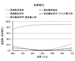
図6は、図1に示す構造の偏光素子1及び図5に示す構造の偏光素子100について、グリッド面側からの入射光に対する吸収軸反射率をシミュレーションにより検証した結果を示すグラフである。図6中、横軸が波長λ(nm)を示しており、縦軸が吸収軸反射率(%)を示している。ここで、吸収軸反射率とは、偏光素子に入射する吸収軸方向(Y軸方向)の偏光(TE波)の反射率を意味する。
FIG. 6 is a graph showing the results of simulating the absorption axis reflectance of the
図6に示すように、グリッド面側から光が入射した場合には、図1及び図5のいずれの構造であっても、第2誘電体層16及び第2吸収層17の機能により、吸収軸反射率が低く抑えられた。
As shown in FIG. 6, when light is incident from the grid surface side, it is absorbed by the functions of the
図7は、図1に示す構造の偏光素子1及び図5に示す構造の偏光素子100について、基板面側からの入射光に対する吸収軸反射率をシミュレーションにより検証した結果を示すグラフである。図7中、横軸が波長λ(nm)を示しており、縦軸が吸収軸反射率(%)を示している。
FIG. 7 is a graph showing the results of simulating the absorption axis reflectance of the
図7に示すように、基板面側から光が入射した場合、図1に示す構造の偏光素子1では、第1吸収層13及び第1誘電体層14の機能により、吸収軸反射率が低く抑えられた。一方、図5に示す構造の偏光素子100では、第1吸収層13及び第1誘電体層14を有しないため、吸収軸反射率が顕著に増大した。
As shown in FIG. 7, when light is incident from the substrate surface side, in the
<実施例2>
実施例2では、図1に示す構造の偏光素子1を実際に作製し、光学特性を検証した。図8は、図1に示す構造の偏光素子1について、透過軸透過率、吸収軸透過率、透過軸反射率、及び吸収軸反射率を検証した結果を示すグラフである。図8中、横軸が波長λ(nm)を示しており、縦軸が透過率又は反射率(%)を示している。ここで、透過軸透過率とは、偏光素子に入射する透過軸方向(X軸方向)の偏光(TM波)の透過率を意味し、透過軸反射率とは、偏光素子に入射する透過軸方向(X軸方向)の偏光(TM波)の反射率を意味する。また、吸収軸透過率とは、偏光素子に入射する吸収軸方向(Y軸方向)の偏光(TE波)の透過率を意味する。
なお、吸収軸反射率については、グリッド面側からの入射光及び基板面側からの入射光の両者について検証し、それ以外の光学特性については、グリッド面側からの入射光について検証した。
<Example 2>
In Example 2, the
The absorption axis reflectance was verified for both the incident light from the grid surface side and the incident light from the substrate surface side, and the other optical characteristics were verified for the incident light from the grid surface side.
図8に示すように、図1に示す構造の偏光素子1では、グリッド面側からの入射光及び基板面側からの入射光の両者について、吸収軸反射率を低く抑えることができ、且つ、他の光学特性への悪影響もなかった。
As shown in FIG. 8, in the
1,1A,1B,1C 偏光素子、10 透明基板、11,11A,11B,11C 格子状凸部、12 台座、13 第1吸収層、14 第1誘電体層、15,15A,15B,15C 反射層、16,16A 第2誘電体層、17,17A 第2吸収層、18 下地層、19 グリッド先端部、100 偏光素子、101 格子状凸部、151 金属層、152 酸化物層 1,1A, 1B, 1C Polarizing element, 10 Transparent substrate, 11, 11A, 11B, 11C Lattice protrusion, 12 pedestal, 13 1st absorption layer, 14 1st dielectric layer, 15, 15A, 15B, 15C Reflection Layer, 16, 16A second dielectric layer, 17, 17A second absorption layer, 18 base layer, 19 grid tip, 100 polarizing element, 101 grid-like convex part, 151 metal layer, 152 oxide layer
Claims (14)
透明基板と、
使用帯域の光の波長よりも短いピッチで前記透明基板上に配列され、所定方向に延在する格子状凸部と、を備え、
前記格子状凸部が、台座と、第1吸収層と、第1誘電体層と、反射層と、第2誘電体層と、第2吸収層と、が前記透明基板側からこの順で連続した構造を有するか、又は、台座と、第1吸収層と、金属膜からなる拡散バリア層と、第1誘電体層と、反射層と、第2誘電体層と、金属膜からなる拡散バリア層と、第2吸収層と、が前記透明基板側からこの順で連続した構造を有し(但し、前記第1誘電体層及び前記第2誘電体層はいずれも、柱状の束で構成されたバンドル構造層を除く。)、
前記台座が、前記所定方向から見たときに、前記透明基板側から前記第1吸収層側に向かうに従い幅が狭まるように側面が傾斜した台形状を有し、
前記第1吸収層の膜厚と前記第2吸収層の膜厚とが略同一であり、且つ、前記第1誘電体層の膜厚と前記第2誘電体層の膜厚とが略同一である偏光素子。 A polarizing element having a wire grid structure.
With a transparent board
It is provided with a grid-like convex portion arranged on the transparent substrate at a pitch shorter than the wavelength of light in the used band and extending in a predetermined direction.
The pedestal, the first absorption layer, the first dielectric layer, the reflection layer, the second dielectric layer, and the second absorption layer are continuous in this order from the transparent substrate side. Diffusion barrier composed of a pedestal, a first absorption layer, a metal film, a first dielectric layer, a reflective layer, a second dielectric layer, and a metal film. The layer and the second absorption layer have a continuous structure in this order from the transparent substrate side (however, the first dielectric layer and the second dielectric layer are both composed of columnar bundles. Excluding the bundle structure layer.),
The pedestal has a trapezoidal shape whose side surfaces are inclined so that the width narrows from the transparent substrate side toward the first absorption layer side when viewed from the predetermined direction.
The film thickness of the first absorption layer and the film thickness of the second absorption layer are substantially the same, and the film thickness of the first dielectric layer and the film thickness of the second dielectric layer are substantially the same. A polarizing element.
透明基板上に、下地層と、第1吸収層と、第1誘電体層と、反射層と、第2誘電体層と、第2吸収層と、が前記透明基板側からこの順で連続した積層体、又は、下地層と、第1吸収層と、金属膜からなる拡散バリア層と、第1誘電体層と、反射層と、第2誘電体層と、金属膜からなる拡散バリア層と、第2吸収層と、が前記透明基板側からこの順で連続した積層体を形成する工程(但し、前記第1誘電体層及び前記第2誘電体層はいずれも、柱状の束で構成されたバンドル構造層を除く。)と、
前記積層体を選択的にエッチングすることにより、使用帯域の光の波長よりも短いピッチで前記透明基板上に配列され、所定方向に延在する格子状凸部を形成する工程と、を有し、
前記格子状凸部が、前記透明基板と前記第1吸収層との間に台座を有し、
前記台座が、前記所定方向から見たときに、前記透明基板側から前記第1吸収層側に向かうに従い幅が狭まるように側面が傾斜した台形状を有し、
前記第1吸収層の膜厚と前記第2吸収層の膜厚とが略同一であり、且つ、前記第1誘電体層の膜厚と前記第2誘電体層の膜厚とが略同一である偏光素子の製造方法。 A method for manufacturing a polarizing element having a wire grid structure.
On the transparent substrate, the base layer, the first absorption layer, the first dielectric layer, the reflection layer, the second dielectric layer, and the second absorption layer are continuous in this order from the transparent substrate side. A laminated body or a base layer, a first absorption layer, a diffusion barrier layer composed of a metal film, a first dielectric layer, a reflection layer, a second dielectric layer, and a diffusion barrier layer composed of a metal film. , A step of forming a continuous laminate in this order from the transparent substrate side with the second absorption layer (however, both the first dielectric layer and the second dielectric layer are composed of columnar bundles. Excluding the bundle structure layer.)
It comprises a step of selectively etching the laminate to form a grid-like convex portion which is arranged on the transparent substrate at a pitch shorter than the wavelength of light in the band used and extends in a predetermined direction. ,
The grid-like convex portion has a pedestal between the transparent substrate and the first absorption layer, and has a pedestal.
The pedestal has a trapezoidal shape whose side surface is inclined so that the width becomes narrower from the transparent substrate side toward the first absorption layer side when viewed from the predetermined direction.
The film thickness of the first absorption layer and the film thickness of the second absorption layer are substantially the same, and the film thickness of the first dielectric layer and the film thickness of the second dielectric layer are substantially the same. A method for manufacturing a certain polarizing element.
Priority Applications (1)
| Application Number | Priority Date | Filing Date | Title |
|---|---|---|---|
| JP2018076824A JP7101028B2 (en) | 2018-04-12 | 2018-04-12 | Polarizing elements, their manufacturing methods, and optical equipment |
Applications Claiming Priority (1)
| Application Number | Priority Date | Filing Date | Title |
|---|---|---|---|
| JP2018076824A JP7101028B2 (en) | 2018-04-12 | 2018-04-12 | Polarizing elements, their manufacturing methods, and optical equipment |
Related Parent Applications (1)
| Application Number | Title | Priority Date | Filing Date |
|---|---|---|---|
| JP2017185286A Division JP6410906B1 (en) | 2017-09-26 | 2017-09-26 | Polarizing element and optical device |
Publications (3)
| Publication Number | Publication Date |
|---|---|
| JP2019061218A JP2019061218A (en) | 2019-04-18 |
| JP2019061218A5 JP2019061218A5 (en) | 2020-09-17 |
| JP7101028B2 true JP7101028B2 (en) | 2022-07-14 |
Family
ID=66177383
Family Applications (1)
| Application Number | Title | Priority Date | Filing Date |
|---|---|---|---|
| JP2018076824A Active JP7101028B2 (en) | 2018-04-12 | 2018-04-12 | Polarizing elements, their manufacturing methods, and optical equipment |
Country Status (1)
| Country | Link |
|---|---|
| JP (1) | JP7101028B2 (en) |
Citations (8)
| Publication number | Priority date | Publication date | Assignee | Title |
|---|---|---|---|---|
| JP2003519818A (en) | 2000-01-11 | 2003-06-24 | モックステック | Embedded wire grid polarizer for the visible spectrum |
| JP2008107394A (en) | 2006-10-23 | 2008-05-08 | Ricoh Co Ltd | Optical element and optical device |
| JP2010066571A (en) | 2008-09-11 | 2010-03-25 | Sony Corp | Polarizing element and production method, and liquid crystal projector |
| JP2012103468A (en) | 2010-11-10 | 2012-05-31 | Asahi Kasei Corp | Optical element and projection type liquid crystal display device |
| JP2012181420A (en) | 2011-03-02 | 2012-09-20 | Sony Chemical & Information Device Corp | Polarization element |
| JP2014052439A (en) | 2012-09-05 | 2014-03-20 | Dexerials Corp | Polarizing element, projector and method for manufacturing polarizing element |
| JP2015034985A (en) | 2013-07-11 | 2015-02-19 | デクセリアルズ株式会社 | Sheet polarizer, sheet polarizer manufacturing method, and bundle structure manufacturing method |
| JP2017083718A (en) | 2015-10-30 | 2017-05-18 | キヤノン株式会社 | Polarization element and using the same |
Family Cites Families (4)
| Publication number | Priority date | Publication date | Assignee | Title |
|---|---|---|---|---|
| JP5682437B2 (en) * | 2010-09-07 | 2015-03-11 | ソニー株式会社 | Solid-state imaging device, solid-state imaging device, imaging apparatus, and polarizing element manufacturing method |
| JP6285131B2 (en) * | 2013-07-10 | 2018-02-28 | デクセリアルズ株式会社 | Polarizing plate and manufacturing method of polarizing plate |
| JP5960319B1 (en) * | 2015-04-30 | 2016-08-02 | デクセリアルズ株式会社 | Polarizing element |
| US10698148B2 (en) * | 2015-10-28 | 2020-06-30 | Dexerials Corporation | Polarizing element and method of producing same |
-
2018
- 2018-04-12 JP JP2018076824A patent/JP7101028B2/en active Active
Patent Citations (8)
| Publication number | Priority date | Publication date | Assignee | Title |
|---|---|---|---|---|
| JP2003519818A (en) | 2000-01-11 | 2003-06-24 | モックステック | Embedded wire grid polarizer for the visible spectrum |
| JP2008107394A (en) | 2006-10-23 | 2008-05-08 | Ricoh Co Ltd | Optical element and optical device |
| JP2010066571A (en) | 2008-09-11 | 2010-03-25 | Sony Corp | Polarizing element and production method, and liquid crystal projector |
| JP2012103468A (en) | 2010-11-10 | 2012-05-31 | Asahi Kasei Corp | Optical element and projection type liquid crystal display device |
| JP2012181420A (en) | 2011-03-02 | 2012-09-20 | Sony Chemical & Information Device Corp | Polarization element |
| JP2014052439A (en) | 2012-09-05 | 2014-03-20 | Dexerials Corp | Polarizing element, projector and method for manufacturing polarizing element |
| JP2015034985A (en) | 2013-07-11 | 2015-02-19 | デクセリアルズ株式会社 | Sheet polarizer, sheet polarizer manufacturing method, and bundle structure manufacturing method |
| JP2017083718A (en) | 2015-10-30 | 2017-05-18 | キヤノン株式会社 | Polarization element and using the same |
Also Published As
| Publication number | Publication date |
|---|---|
| JP2019061218A (en) | 2019-04-18 |
Similar Documents
| Publication | Publication Date | Title |
|---|---|---|
| JP6230689B1 (en) | Polarizing plate, method for producing the same, and optical instrument | |
| JP6410906B1 (en) | Polarizing element and optical device | |
| JP6302040B1 (en) | Polarizing plate, method for producing the same, and optical instrument | |
| JP6577641B2 (en) | Polarizing plate, method for producing the same, and optical instrument | |
| WO2019159982A1 (en) | Polarizing plate, method of manufacturing the same, and optical apparatus | |
| JP6484373B1 (en) | Polarizing plate and optical apparatus including the same | |
| US11971568B2 (en) | Polarizing plate, manufacturing method thereof, and optical device | |
| US11630254B2 (en) | Wire grid polarizing plate having trapezoidal absorption layer | |
| JP7101028B2 (en) | Polarizing elements, their manufacturing methods, and optical equipment | |
| JP7394020B2 (en) | Polarizing plate and its manufacturing method, and optical equipment | |
| JP6935318B2 (en) | Polarizing plate and its manufacturing method, and optical equipment | |
| JP7333168B2 (en) | POLARIZING ELEMENT, POLARIZING ELEMENT MANUFACTURING METHOD, AND OPTICAL DEVICE | |
| JP7075372B2 (en) | Polarizing plate and its manufacturing method, and optical equipment | |
| JP2020003771A (en) | Polarizer manufacturing method | |
| JP7219735B2 (en) | Polarizing plate, manufacturing method thereof, and optical device | |
| WO2021230275A1 (en) | Polarization plate, production method therefor, and optical instrument | |
| WO2023145307A1 (en) | Wire-grid polarizer, manufacturing method therefor, and optical device | |
| JP2020086426A (en) | Polarizer and optical device having the same | |
| CN111198413A (en) | Polarizing plate and optical device having the same |
Legal Events
| Date | Code | Title | Description |
|---|---|---|---|
| A521 | Request for written amendment filed |
Free format text: JAPANESE INTERMEDIATE CODE: A523 Effective date: 20200804 |
|
| A621 | Written request for application examination |
Free format text: JAPANESE INTERMEDIATE CODE: A621 Effective date: 20200804 |
|
| A131 | Notification of reasons for refusal |
Free format text: JAPANESE INTERMEDIATE CODE: A131 Effective date: 20210907 |
|
| A521 | Request for written amendment filed |
Free format text: JAPANESE INTERMEDIATE CODE: A523 Effective date: 20211028 |
|
| A131 | Notification of reasons for refusal |
Free format text: JAPANESE INTERMEDIATE CODE: A131 Effective date: 20220301 |
|
| A521 | Request for written amendment filed |
Free format text: JAPANESE INTERMEDIATE CODE: A523 Effective date: 20220325 |
|
| A131 | Notification of reasons for refusal |
Free format text: JAPANESE INTERMEDIATE CODE: A131 Effective date: 20220412 |
|
| A521 | Request for written amendment filed |
Free format text: JAPANESE INTERMEDIATE CODE: A523 Effective date: 20220606 |
|
| TRDD | Decision of grant or rejection written | ||
| A01 | Written decision to grant a patent or to grant a registration (utility model) |
Free format text: JAPANESE INTERMEDIATE CODE: A01 Effective date: 20220621 |
|
| A61 | First payment of annual fees (during grant procedure) |
Free format text: JAPANESE INTERMEDIATE CODE: A61 Effective date: 20220704 |
|
| R150 | Certificate of patent or registration of utility model |
Ref document number: 7101028 Country of ref document: JP Free format text: JAPANESE INTERMEDIATE CODE: R150 |