JP7083601B2 - Electronics - Google Patents
Electronics Download PDFInfo
- Publication number
- JP7083601B2 JP7083601B2 JP2017136111A JP2017136111A JP7083601B2 JP 7083601 B2 JP7083601 B2 JP 7083601B2 JP 2017136111 A JP2017136111 A JP 2017136111A JP 2017136111 A JP2017136111 A JP 2017136111A JP 7083601 B2 JP7083601 B2 JP 7083601B2
- Authority
- JP
- Japan
- Prior art keywords
- wiring
- transistor
- terminal
- circuit
- memory cell
- Prior art date
- Legal status (The legal status is an assumption and is not a legal conclusion. Google has not performed a legal analysis and makes no representation as to the accuracy of the status listed.)
- Active
Links
Images


Classifications
-
- G—PHYSICS
- G06—COMPUTING; CALCULATING OR COUNTING
- G06T—IMAGE DATA PROCESSING OR GENERATION, IN GENERAL
- G06T1/00—General purpose image data processing
- G06T1/60—Memory management
-
- G—PHYSICS
- G06—COMPUTING; CALCULATING OR COUNTING
- G06F—ELECTRIC DIGITAL DATA PROCESSING
- G06F1/00—Details not covered by groups G06F3/00 - G06F13/00 and G06F21/00
- G06F1/16—Constructional details or arrangements
- G06F1/1613—Constructional details or arrangements for portable computers
- G06F1/1633—Constructional details or arrangements of portable computers not specific to the type of enclosures covered by groups G06F1/1615 - G06F1/1626
- G06F1/1637—Details related to the display arrangement, including those related to the mounting of the display in the housing
- G06F1/1652—Details related to the display arrangement, including those related to the mounting of the display in the housing the display being flexible, e.g. mimicking a sheet of paper, or rollable
-
- G—PHYSICS
- G06—COMPUTING; CALCULATING OR COUNTING
- G06F—ELECTRIC DIGITAL DATA PROCESSING
- G06F1/00—Details not covered by groups G06F3/00 - G06F13/00 and G06F21/00
- G06F1/26—Power supply means, e.g. regulation thereof
- G06F1/32—Means for saving power
- G06F1/3203—Power management, i.e. event-based initiation of a power-saving mode
- G06F1/3206—Monitoring of events, devices or parameters that trigger a change in power modality
- G06F1/3215—Monitoring of peripheral devices
- G06F1/3218—Monitoring of peripheral devices of display devices
-
- G—PHYSICS
- G06—COMPUTING; CALCULATING OR COUNTING
- G06F—ELECTRIC DIGITAL DATA PROCESSING
- G06F1/00—Details not covered by groups G06F3/00 - G06F13/00 and G06F21/00
- G06F1/26—Power supply means, e.g. regulation thereof
- G06F1/32—Means for saving power
- G06F1/3203—Power management, i.e. event-based initiation of a power-saving mode
- G06F1/3234—Power saving characterised by the action undertaken
- G06F1/325—Power saving in peripheral device
- G06F1/3265—Power saving in display device
-
- G—PHYSICS
- G06—COMPUTING; CALCULATING OR COUNTING
- G06F—ELECTRIC DIGITAL DATA PROCESSING
- G06F13/00—Interconnection of, or transfer of information or other signals between, memories, input/output devices or central processing units
- G06F13/38—Information transfer, e.g. on bus
- G06F13/40—Bus structure
- G06F13/4063—Device-to-bus coupling
- G06F13/4068—Electrical coupling
-
- G—PHYSICS
- G06—COMPUTING; CALCULATING OR COUNTING
- G06F—ELECTRIC DIGITAL DATA PROCESSING
- G06F3/00—Input arrangements for transferring data to be processed into a form capable of being handled by the computer; Output arrangements for transferring data from processing unit to output unit, e.g. interface arrangements
- G06F3/01—Input arrangements or combined input and output arrangements for interaction between user and computer
- G06F3/03—Arrangements for converting the position or the displacement of a member into a coded form
- G06F3/041—Digitisers, e.g. for touch screens or touch pads, characterised by the transducing means
- G06F3/0416—Control or interface arrangements specially adapted for digitisers
-
- G—PHYSICS
- G09—EDUCATION; CRYPTOGRAPHY; DISPLAY; ADVERTISING; SEALS
- G09G—ARRANGEMENTS OR CIRCUITS FOR CONTROL OF INDICATING DEVICES USING STATIC MEANS TO PRESENT VARIABLE INFORMATION
- G09G3/00—Control arrangements or circuits, of interest only in connection with visual indicators other than cathode-ray tubes
- G09G3/20—Control arrangements or circuits, of interest only in connection with visual indicators other than cathode-ray tubes for presentation of an assembly of a number of characters, e.g. a page, by composing the assembly by combination of individual elements arranged in a matrix no fixed position being assigned to or needed to be assigned to the individual characters or partial characters
- G09G3/2092—Details of a display terminals using a flat panel, the details relating to the control arrangement of the display terminal and to the interfaces thereto
- G09G3/2096—Details of the interface to the display terminal specific for a flat panel
-
- G—PHYSICS
- G09—EDUCATION; CRYPTOGRAPHY; DISPLAY; ADVERTISING; SEALS
- G09G—ARRANGEMENTS OR CIRCUITS FOR CONTROL OF INDICATING DEVICES USING STATIC MEANS TO PRESENT VARIABLE INFORMATION
- G09G3/00—Control arrangements or circuits, of interest only in connection with visual indicators other than cathode-ray tubes
- G09G3/20—Control arrangements or circuits, of interest only in connection with visual indicators other than cathode-ray tubes for presentation of an assembly of a number of characters, e.g. a page, by composing the assembly by combination of individual elements arranged in a matrix no fixed position being assigned to or needed to be assigned to the individual characters or partial characters
- G09G3/22—Control arrangements or circuits, of interest only in connection with visual indicators other than cathode-ray tubes for presentation of an assembly of a number of characters, e.g. a page, by composing the assembly by combination of individual elements arranged in a matrix no fixed position being assigned to or needed to be assigned to the individual characters or partial characters using controlled light sources
- G09G3/30—Control arrangements or circuits, of interest only in connection with visual indicators other than cathode-ray tubes for presentation of an assembly of a number of characters, e.g. a page, by composing the assembly by combination of individual elements arranged in a matrix no fixed position being assigned to or needed to be assigned to the individual characters or partial characters using controlled light sources using electroluminescent panels
- G09G3/32—Control arrangements or circuits, of interest only in connection with visual indicators other than cathode-ray tubes for presentation of an assembly of a number of characters, e.g. a page, by composing the assembly by combination of individual elements arranged in a matrix no fixed position being assigned to or needed to be assigned to the individual characters or partial characters using controlled light sources using electroluminescent panels semiconductive, e.g. using light-emitting diodes [LED]
- G09G3/3208—Control arrangements or circuits, of interest only in connection with visual indicators other than cathode-ray tubes for presentation of an assembly of a number of characters, e.g. a page, by composing the assembly by combination of individual elements arranged in a matrix no fixed position being assigned to or needed to be assigned to the individual characters or partial characters using controlled light sources using electroluminescent panels semiconductive, e.g. using light-emitting diodes [LED] organic, e.g. using organic light-emitting diodes [OLED]
- G09G3/3275—Details of drivers for data electrodes
- G09G3/3291—Details of drivers for data electrodes in which the data driver supplies a variable data voltage for setting the current through, or the voltage across, the light-emitting elements
-
- G—PHYSICS
- G09—EDUCATION; CRYPTOGRAPHY; DISPLAY; ADVERTISING; SEALS
- G09G—ARRANGEMENTS OR CIRCUITS FOR CONTROL OF INDICATING DEVICES USING STATIC MEANS TO PRESENT VARIABLE INFORMATION
- G09G3/00—Control arrangements or circuits, of interest only in connection with visual indicators other than cathode-ray tubes
- G09G3/20—Control arrangements or circuits, of interest only in connection with visual indicators other than cathode-ray tubes for presentation of an assembly of a number of characters, e.g. a page, by composing the assembly by combination of individual elements arranged in a matrix no fixed position being assigned to or needed to be assigned to the individual characters or partial characters
- G09G3/34—Control arrangements or circuits, of interest only in connection with visual indicators other than cathode-ray tubes for presentation of an assembly of a number of characters, e.g. a page, by composing the assembly by combination of individual elements arranged in a matrix no fixed position being assigned to or needed to be assigned to the individual characters or partial characters by control of light from an independent source
- G09G3/36—Control arrangements or circuits, of interest only in connection with visual indicators other than cathode-ray tubes for presentation of an assembly of a number of characters, e.g. a page, by composing the assembly by combination of individual elements arranged in a matrix no fixed position being assigned to or needed to be assigned to the individual characters or partial characters by control of light from an independent source using liquid crystals
- G09G3/3611—Control of matrices with row and column drivers
- G09G3/3685—Details of drivers for data electrodes
- G09G3/3688—Details of drivers for data electrodes suitable for active matrices only
-
- G—PHYSICS
- G09—EDUCATION; CRYPTOGRAPHY; DISPLAY; ADVERTISING; SEALS
- G09G—ARRANGEMENTS OR CIRCUITS FOR CONTROL OF INDICATING DEVICES USING STATIC MEANS TO PRESENT VARIABLE INFORMATION
- G09G2300/00—Aspects of the constitution of display devices
- G09G2300/04—Structural and physical details of display devices
- G09G2300/0439—Pixel structures
- G09G2300/046—Pixel structures with an emissive area and a light-modulating area combined in one pixel
-
- G—PHYSICS
- G09—EDUCATION; CRYPTOGRAPHY; DISPLAY; ADVERTISING; SEALS
- G09G—ARRANGEMENTS OR CIRCUITS FOR CONTROL OF INDICATING DEVICES USING STATIC MEANS TO PRESENT VARIABLE INFORMATION
- G09G2300/00—Aspects of the constitution of display devices
- G09G2300/08—Active matrix structure, i.e. with use of active elements, inclusive of non-linear two terminal elements, in the pixels together with light emitting or modulating elements
- G09G2300/0809—Several active elements per pixel in active matrix panels
- G09G2300/0814—Several active elements per pixel in active matrix panels used for selection purposes, e.g. logical AND for partial update
-
- G—PHYSICS
- G09—EDUCATION; CRYPTOGRAPHY; DISPLAY; ADVERTISING; SEALS
- G09G—ARRANGEMENTS OR CIRCUITS FOR CONTROL OF INDICATING DEVICES USING STATIC MEANS TO PRESENT VARIABLE INFORMATION
- G09G2320/00—Control of display operating conditions
- G09G2320/02—Improving the quality of display appearance
- G09G2320/029—Improving the quality of display appearance by monitoring one or more pixels in the display panel, e.g. by monitoring a fixed reference pixel
- G09G2320/0295—Improving the quality of display appearance by monitoring one or more pixels in the display panel, e.g. by monitoring a fixed reference pixel by monitoring each display pixel
-
- G—PHYSICS
- G09—EDUCATION; CRYPTOGRAPHY; DISPLAY; ADVERTISING; SEALS
- G09G—ARRANGEMENTS OR CIRCUITS FOR CONTROL OF INDICATING DEVICES USING STATIC MEANS TO PRESENT VARIABLE INFORMATION
- G09G2330/00—Aspects of power supply; Aspects of display protection and defect management
- G09G2330/02—Details of power systems and of start or stop of display operation
- G09G2330/021—Power management, e.g. power saving
-
- G—PHYSICS
- G09—EDUCATION; CRYPTOGRAPHY; DISPLAY; ADVERTISING; SEALS
- G09G—ARRANGEMENTS OR CIRCUITS FOR CONTROL OF INDICATING DEVICES USING STATIC MEANS TO PRESENT VARIABLE INFORMATION
- G09G2360/00—Aspects of the architecture of display systems
- G09G2360/12—Frame memory handling
-
- Y—GENERAL TAGGING OF NEW TECHNOLOGICAL DEVELOPMENTS; GENERAL TAGGING OF CROSS-SECTIONAL TECHNOLOGIES SPANNING OVER SEVERAL SECTIONS OF THE IPC; TECHNICAL SUBJECTS COVERED BY FORMER USPC CROSS-REFERENCE ART COLLECTIONS [XRACs] AND DIGESTS
- Y02—TECHNOLOGIES OR APPLICATIONS FOR MITIGATION OR ADAPTATION AGAINST CLIMATE CHANGE
- Y02D—CLIMATE CHANGE MITIGATION TECHNOLOGIES IN INFORMATION AND COMMUNICATION TECHNOLOGIES [ICT], I.E. INFORMATION AND COMMUNICATION TECHNOLOGIES AIMING AT THE REDUCTION OF THEIR OWN ENERGY USE
- Y02D10/00—Energy efficient computing, e.g. low power processors, power management or thermal management
Description
本発明の一態様は、電子機器に関する。 One aspect of the present invention relates to an electronic device.
なお本発明の一態様は、上記の技術分野に限定されない。本明細書等で開示する発明の技術分野は、物、方法、又は、製造方法に関するものである。又は、本発明の一態様は、プロセス、マシン、マニュファクチャ、又は、組成物(コンポジション・オブ・マター)に関するものである。そのため、より具体的に本明細書で開示する本発明の一態様の技術分野としては、半導体装置、表示装置、液晶表示装置、発光装置、蓄電装置、撮像装置、記憶装置、プロセッサ、電子機器、それらの駆動方法、それらの製造方法、それらの検査方法、又はそれらのシステムを一例として挙げることができる。 It should be noted that one aspect of the present invention is not limited to the above technical fields. The technical field of the invention disclosed in the present specification and the like relates to a product, a method, or a manufacturing method. Alternatively, one aspect of the invention relates to a process, machine, manufacture, or composition (composition of matter). Therefore, more specifically, the technical fields of one aspect of the present invention disclosed in the present specification include semiconductor devices, display devices, liquid crystal display devices, light emitting devices, power storage devices, image pickup devices, storage devices, processors, electronic devices, and the like. Examples thereof include their driving methods, their manufacturing methods, their inspection methods, or their systems.
近年、スマートフォンなどの携帯電話、タブレット型情報端末、ノート型PC(パーソナルコンピュータ)等が有する表示装置において、様々な面で改良が進められている。例えば、解像度を大きくする、色再現性(NTSC比)を高くする、駆動回路を小さくする、消費電力を低減する、等の表示装置の開発が行われている。 In recent years, improvements have been made in various aspects in display devices possessed by mobile phones such as smartphones, tablet-type information terminals, notebook-type PCs (personal computers), and the like. For example, display devices such as increasing the resolution, increasing the color reproducibility (NTSC ratio), reducing the drive circuit, and reducing the power consumption are being developed.
また、改良の1つとして、環境の光に応じて、表示装置に映す画像の明るさを自動的に調節する機能を有する表示装置が挙げられる。該表示装置として、例えば、環境の光を反射して画像を映す機能と、発光素子を光らせて画像を映す機能と、を有する表示装置が挙げられる。この構成にすることにより、環境の光が十分に強い場合には、反射光を利用して表示装置に画像を映す表示モード(以下、反射モードという。)とし、又は環境の光が弱い場合には、発光素子を光らせて表示装置に画像を映す表示モード(以下、自発光モードという。)として、表示装置に映す画像の明るさの調節を行うことができる。つまり、該表示装置は、照度計(照度センサという場合もある。)などを用いて環境の光を検知することによって、該光の強さに応じて表示方法を反射モード、自発光モード、又はそれら両方を用いたモードのいずれかを選択して、画像の表示を行うことができる。 Further, as one of the improvements, there is a display device having a function of automatically adjusting the brightness of the image displayed on the display device according to the light of the environment. Examples of the display device include a display device having a function of reflecting the light of the environment to project an image and a function of illuminating a light emitting element to project an image. With this configuration, when the ambient light is sufficiently strong, the display mode (hereinafter referred to as the reflection mode) in which the image is displayed on the display device using the reflected light is set, or when the environmental light is weak. Can adjust the brightness of the image displayed on the display device as a display mode (hereinafter referred to as self-luminous mode) in which the light emitting element is illuminated and the image is displayed on the display device. That is, the display device detects the light of the environment by using an illuminance meter (sometimes called an illuminance sensor), and the display method is changed to the reflection mode, the self-luminous mode, or the self-luminous mode according to the intensity of the light. The image can be displayed by selecting one of the modes using both of them.
ところで、発光素子を光らせて画像を映す機能と、環境の光を反射して画像を映す機能と、を有する表示装置として、例えば、1つの画素に、液晶素子を制御する画素回路と、発光素子を制御する画素回路と、を有する表示装置(以下、ハイブリッド(複合型)表示装置という。)が特許文献1乃至特許文献3に開示されている。
By the way, as a display device having a function of illuminating a light emitting element to project an image and a function of reflecting environmental light to project an image, for example, a pixel circuit for controlling a liquid crystal element in one pixel and a light emitting element. A display device having a pixel circuit for controlling the above (hereinafter referred to as a hybrid (composite type) display device) is disclosed in
ところで、表示装置に映すための画像処理として、ニューラルネットワークの利用が検討されている。非特許文献1には、ニューラルネットワークによる自己学習機能を備えたチップに関する技術が記載されている。
By the way, the use of a neural network is being studied as an image process for displaying on a display device. Non-Patent
表示装置の表示素子(反射素子、液晶素子、発光素子など)が有する選択トランジスタとして、オフ電流が低い特性を有するトランジスタを用いることにより、該表示素子に、長時間、電荷(画像データ)を保持することができる。これは、選択トランジスタが非導通状態のときのオフ電流が低いため、表示素子からの電荷(画像データ)のリークが起こりにくくなるためである。特に、表示装置が静止画を表示する場合において、表示素子が保持している画像データのリフレッシュの必要が無くなるため、表示品質を保ったまま、消費電力を低減することができる。また、この場合、画像データの書き換えも行う必要が無くなるため、表示装置を駆動するソースドライバ、及びゲートドライバをパワーゲーティングして、表示装置の消費電力を低減することができる。このように、表示装置が静止画を表示しているときに、必要のない回路をパワーゲーティングする駆動方法を、本明細書では、アイドリングストップ駆動(又は、IDS駆動)と呼称する。 By using a transistor having a characteristic of low off-current as a selection transistor of a display element (reflection element, liquid crystal element, light emitting element, etc.) of a display device, the display element retains an electric charge (image data) for a long time. can do. This is because the off-current is low when the selection transistor is in the non-conducting state, so that the leakage of electric charge (image data) from the display element is less likely to occur. In particular, when the display device displays a still image, it is not necessary to refresh the image data held by the display element, so that the power consumption can be reduced while maintaining the display quality. Further, in this case, since it is not necessary to rewrite the image data, it is possible to reduce the power consumption of the display device by power gating the source driver and the gate driver that drive the display device. As described above, a driving method for power-gating an unnecessary circuit when the display device is displaying a still image is referred to as an idling stop drive (or IDS drive) in the present specification.
表示装置のアイドリングストップ駆動は、画像データの更新が無いことを検知し、その検知をトリガとして実行することができる。また、アイドリングストップ駆動を行うタイミングに合わせて、表示装置に備わるソースドライバ、ゲートドライバ、画像の補正回路などをパワーゲーティングすることができる。画像データの更新が無いことを検知する方法として、例えば、表示装置において、1フレームの画像データの表示が終了して、その次のフレームの画像データが送られてこないことをソースドライバなどによって判断する、又は、適当な回路が画像データの更新が無いことを示す制御信号を送信して知らせる、などといった方法が挙げられる。 The idling stop drive of the display device can detect that there is no update of the image data and execute the detection as a trigger. In addition, the source driver, gate driver, image correction circuit, etc. provided in the display device can be power-gated according to the timing of idling stop drive. As a method of detecting that the image data is not updated, for example, the source driver determines that the display of the image data of one frame is finished and the image data of the next frame is not sent in the display device. Alternatively, a suitable circuit may transmit a control signal indicating that the image data has not been updated to notify the user.
ところで、表示装置に備わる各回路をパワーゲーティングする場合、パワーゲーティングの事前に、レジスタなどの記憶装置に設定データをセーブする必要がある。データのセーブには、表示装置の各回路を動作する必要があり、換言すると、セーブが完了するまで、表示装置の各回路をパワーゲーティングすることができない。つまり、上述した検知方法によって、画像データの更新が無い事を検知してデータのセーブを行おうとすると、データセーブするまでは表示装置の各回路が動作し続けるため、各回路がパワーゲーティングするまでに必要な時間が長くなる。そのため、各回路のパワーゲーティングの正味の期間が短くなってしまい、表示装置の各回路に対してパワーゲーティングすることによる消費電力の低減効果が、小さくなる場合がある。 By the way, when power gating each circuit provided in a display device, it is necessary to save the setting data in a storage device such as a register before power gating. In order to save data, it is necessary to operate each circuit of the display device, in other words, it is not possible to power gate each circuit of the display device until the save is completed. In other words, if an attempt is made to save data by detecting that the image data has not been updated by the above-mentioned detection method, each circuit of the display device will continue to operate until the data is saved, so that each circuit will continue to operate until power gating. The time required for this will be longer. Therefore, the net period of power gating of each circuit may be shortened, and the effect of reducing power consumption by power gating for each circuit of the display device may be reduced.
本発明の一態様は、新規な電子機器を提供することを課題の一つとする。又は、本発明の一態様は、新規な電子機器の動作方法を提供することを課題の一とする。 One aspect of the present invention is to provide a novel electronic device. Alternatively, one aspect of the present invention is to provide a new method of operating an electronic device.
又は、本発明の一態様は、表示品質が高い電子機器を提供することを課題の一とする。又は、本発明の一態様は、消費電力が低減された電子機器を提供することを課題の一とする。 Alternatively, one aspect of the present invention is to provide an electronic device having high display quality. Alternatively, one aspect of the present invention is to provide an electronic device with reduced power consumption.
なお本発明の一態様の課題は、上記列挙した課題に限定されない。上記列挙した課題は、他の課題の存在を妨げるものではない。なお他の課題は、以下の記載で述べる、本項目で言及していない課題である。本項目で言及していない課題は、当業者であれば明細書又は図面等の記載から導き出せるものであり、これらの記載から適宜抽出することができる。なお、本発明の一態様は、上記列挙した記載、及び他の課題のうち、少なくとも一つの課題を解決するものである。なお、本発明の一態様は、上記列挙した記載、及び他の課題の全てを解決する必要はない。 The problems of one aspect of the present invention are not limited to the problems listed above. The issues listed above do not preclude the existence of other issues. Other issues are issues not mentioned in this item, which are described below. Issues not mentioned in this item can be derived from the description of the description, drawings, etc. by those skilled in the art, and can be appropriately extracted from these descriptions. In addition, one aspect of the present invention solves at least one of the above-listed descriptions and other problems. It should be noted that one aspect of the present invention does not need to solve all of the above-listed descriptions and other problems.
(1)
本発明の一態様は、情報処理回路と、フレームメモリと、記憶装置と、を有する電子機器であり、フレームメモリは、消費電力モニタを有し、情報処理回路は、第1積和演算回路と、第2積和演算回路と、第1スイッチ回路と、第2スイッチ回路と、を有し、第1積和演算回路は、第1端子を有し、第2積和演算回路は、第2端子を有し、第1スイッチ回路は、第3端子と、第4端子と、を有し、第2スイッチ回路は、第5端子と、第6端子と、を有し、第1端子は、第3端子と電気的に接続され、第2端子は、第5端子と電気的に接続され、第4端子は、第6端子と電気的に接続され、第1スイッチ回路は、第3端子と、第4端子と、の間を導通状態、又は非導通状態にする機能を有し、第2スイッチ回路は、第5端子と、第6端子と、の間を導通状態、又は非導通状態にする機能を有し、フレームメモリは、画像データを保持する機能と、保持した該画像データを書き換える機能と、を有し、消費電力モニタは、フレームメモリに保持した画像データを書き換えた場合に生じる消費電力量を第1データとして取得する機能を有し、情報処理回路は、第1データと、アイドリングストップ駆動の有無を知らせる信号と、を受け取る機能と、第1データと、信号と、に応じて、記憶装置にデータセーブを投機実行するか否かを判定する機能を有することを特徴とする電子機器である。
(1)
One aspect of the present invention is an electronic device having an information processing circuit, a frame memory, and a storage device, the frame memory has a power consumption monitor, and the information processing circuit is a first product-sum calculation circuit. , A second product-sum calculation circuit, a first switch circuit, and a second switch circuit, the first product-sum calculation circuit has a first terminal, and the second product-sum calculation circuit has a second. The first switch circuit has a third terminal and a fourth terminal, the second switch circuit has a fifth terminal and a sixth terminal, and the first terminal has a terminal. The second terminal is electrically connected to the third terminal, the second terminal is electrically connected to the fifth terminal, the fourth terminal is electrically connected to the sixth terminal, and the first switch circuit is electrically connected to the third terminal. The second switch circuit has a function of making a conductive state or a non-conducting state between the fourth terminal and the fourth terminal, and the second switch circuit makes a conductive state or a non-conducting state between the fifth terminal and the sixth terminal. The frame memory has a function of holding the image data and a function of rewriting the held image data, and the power consumption monitor occurs when the image data held in the frame memory is rewritten. It has a function to acquire the amount of power consumption as the first data, and the information processing circuit responds to the first data, the function of receiving the signal indicating the presence or absence of idling stop drive, the first data, and the signal. The electronic device is characterized in that the storage device has a function of determining whether or not to speculatively execute data saving.
(2)
又は、本発明の一態様は、情報処理回路と、タッチセンサユニットと、記憶装置と、を有し、情報処理回路は、第1積和演算回路と、第2積和演算回路と、第1スイッチ回路と、第2スイッチ回路と、を有し、第1積和演算回路は、第1端子を有し、第2積和演算回路は、第2端子を有し、第1スイッチ回路は、第3端子と、第4端子と、を有し、第2スイッチ回路は、第5端子と、第6端子と、を有し、第1端子は、第3端子と電気的に接続され、第2端子は、第5端子と電気的に接続され、第4端子は、第6端子と電気的に接続され、第1スイッチ回路は、第3端子と、第4端子と、の間を導通状態、又は非導通状態にする機能を有し、第2スイッチ回路は、第5端子と、第6端子と、の間を導通状態、又は非導通状態にする機能を有し、タッチセンサユニットは、入力された情報に基づく第1データを取得する機能を有し、情報処理回路は、第1データと、アイドリングストップ駆動の有無を知らせる信号と、を受け取る機能と、第1データと、信号と、に応じて、記憶装置にデータセーブを投機実行するか否かを判定する機能を有することを特徴とする電子機器である。
(2)
Alternatively, one aspect of the present invention includes an information processing circuit, a touch sensor unit, and a storage device, and the information processing circuit includes a first product-sum calculation circuit, a second product-sum calculation circuit, and a first. It has a switch circuit and a second switch circuit, the first product-sum calculation circuit has a first terminal, the second product-sum calculation circuit has a second terminal, and the first switch circuit has a first terminal. It has a third terminal and a fourth terminal, the second switch circuit has a fifth terminal and a sixth terminal, and the first terminal is electrically connected to the third terminal and has a third terminal. The 2nd terminal is electrically connected to the 5th terminal, the 4th terminal is electrically connected to the 6th terminal, and the 1st switch circuit is in a conductive state between the 3rd terminal and the 4th terminal. The second switch circuit has a function of making the fifth terminal and the sixth terminal in a conductive state or a non-conducting state, and the touch sensor unit has a function of making the touch sensor unit in a conductive state or a non-conducting state. The information processing circuit has a function of acquiring the first data based on the input information, and the information processing circuit has a function of receiving the first data and a signal notifying the presence or absence of idling stop drive, the first data, and a signal. It is an electronic device characterized in that it has a function of determining whether or not to speculatively execute data saving in a storage device according to the above.
(3)
又は、本発明の一態様は、前記(1)、又は前記(2)において、第1スイッチ回路の構成は、第2スイッチ回路と同じ構成であり、第5端子は、第3端子に相当し、第6端子は、第4端子に相当し、第1スイッチ回路は、回路を有し、回路は、第1トランジスタと、第2トランジスタと、第1容量素子と、を有し、第1トランジスタのソース又はドレインの一方は、第2トランジスタのゲートと電気的に接続され、第1容量素子の1対の電極の一方は、第1トランジスタのソース又はドレインの一方と電気的に接続され、第2トランジスタのソース又はドレインの一方は、第3端子と電気的に接続され、第2トランジスタのソース又はドレインの他方は、第4端子と電気的に接続されることを特徴とする電子機器である。
(3)
Alternatively, in one aspect of the present invention, in the above (1) or (2), the configuration of the first switch circuit is the same as that of the second switch circuit, and the fifth terminal corresponds to the third terminal. The sixth terminal corresponds to the fourth terminal, the first switch circuit has a circuit, and the circuit has a first transistor, a second transistor, and a first capacitive element, and the first transistor. One of the source or drain of the first transistor is electrically connected to the gate of the second transistor, and one of the pair of electrodes of the first capacitive element is electrically connected to one of the source or drain of the first transistor. One of the source or drain of the two transistors is electrically connected to the third terminal, and the other of the source or drain of the second transistor is electrically connected to the fourth terminal. ..
(4)
又は、本発明の一態様は、前記(3)において、第1トランジスタと、第2トランジスタと、の少なくとも一のチャネル形成領域は、インジウム、元素M(元素Mはアルミニウム、ガリウム、イットリウム、またはスズ)、亜鉛の少なくとも一を含む酸化物を有することを特徴とする電子機器である。
(4)
Alternatively, in one aspect of the present invention, in the above (3), at least one channel forming region of the first transistor and the second transistor is indium, element M (element M is aluminum, gallium, yttrium, or tin). ), An electronic device characterized by having an oxide containing at least one of zinc.
(5)
又は、本発明の一態様は、前記(1)乃至(4)のいずれか一において、第2積和演算回路の構成は、第1積和演算回路と同じ構成であり、第1積和演算回路は、第1メモリセルと、第2メモリセルと、オフセット回路と、を有し、第1メモリセルは、オフセット回路と電気的に接続され、第2メモリセルは、オフセット回路と電気的に接続され、第1メモリセルは、第1アナログデータを保持する機能と、第1メモリセルに第1信号を選択信号として印加されたときに、第1アナログデータに応じた第1電流を流す機能と、を有し、第2メモリセルは、参照アナログデータを保持する機能と、第2メモリセルに第1信号が選択信号として印加されたときに、参照アナログデータに応じた第2電流を流す機能と、を有し、オフセット回路は、第1電流と第2電流との差の第3電流を流す機能を有し、第1メモリセルは、第1メモリセルに、第2アナログデータを有する第2信号が選択信号として印加されたときに、第2信号と、第1アナログデータと、に応じた第4電流を流す機能と、を有し、第2メモリセルは、第2メモリセルに第2信号が選択信号として印加されたときに、第2信号と、参照アナログデータと、に応じた第5電流を流す機能と、を有し、第1積和演算回路は、第4電流と第5電流との差から第3電流を差し引いた第6電流を出力する機能を有することを特徴とする電子機器である。
(5)
Alternatively, in one aspect of the present invention, in any one of the above (1) to (4), the configuration of the second product-sum calculation circuit is the same as that of the first product-sum calculation circuit, and the first product-sum calculation is performed. The circuit has a first memory cell, a second memory cell, and an offset circuit, the first memory cell is electrically connected to the offset circuit, and the second memory cell is electrically connected to the offset circuit. The connected first memory cell has a function of holding the first analog data and a function of passing a first current corresponding to the first analog data when the first signal is applied to the first memory cell as a selection signal. The second memory cell has a function of holding reference analog data, and when a first signal is applied to the second memory cell as a selection signal, a second current corresponding to the reference analog data is passed. The offset circuit has a function of passing a third current, which is the difference between the first current and the second current, and the first memory cell has the second analog data in the first memory cell. When the second signal is applied as a selection signal, it has a function of passing a fourth current according to the second signal, the first analog data, and the second memory cell becomes a second memory cell. When the second signal is applied as a selection signal, it has a function of passing a fifth current according to the second signal, reference analog data, and the first product-sum calculation circuit has a fourth current. It is an electronic device characterized by having a function of outputting a sixth current obtained by subtracting a third current from a difference from the fifth current.
(6)
又は、本発明の一態様は、前記(1)乃至(4)のいずれか一において、オフセット回路を有し、第2積和演算回路の構成は、第1積和演算回路と同じ構成であり、第1積和演算回路は、メモリセルアレイを有し、メモリセルアレイは、第1メモリセルと、第2メモリセルと、を有し、第1メモリセルは、オフセット回路と電気的に接続され、第2メモリセルは、オフセット回路と電気的に接続され、第1メモリセルは、第1アナログデータにを保持する機能と、第1メモリセルに第1信号が選択信号として印加されたときに、第1アナログデータに応じた第1電流を流す機能と、を有し、第2メモリセルは、参照アナログデータを保持する機能と、第2メモリセルに第1信号が選択信号として印加されたときに、参照アナログデータに応じた第2電流を流す機能と、を有し、オフセット回路は、第1電流と第2電流との差の第3電流を流す機能を有し、第1メモリセルは、第1メモリセルに、第2アナログデータを有する第2信号が選択信号として印加されたときに、第2信号と、第1アナログデータと、に応じた第4電流を流す機能と、を有し、第2メモリセルは、第2メモリセルに、第2信号が選択信号として印加されたときに、第2信号と、参照アナログデータと、に応じた第5電流を流す機能と、を有し、第1積和演算回路は、第4電流と第5電流との差から第3電流を差し引いた第6電流を出力する機能を有することを特徴とする電子機器である。
(6)
Alternatively, one aspect of the present invention has an offset circuit in any one of (1) to (4) above, and the configuration of the second product-sum calculation circuit is the same as that of the first product-sum calculation circuit. The first product-sum operation circuit has a memory cell array, the memory cell array has a first memory cell and a second memory cell, and the first memory cell is electrically connected to the offset circuit. The second memory cell is electrically connected to the offset circuit, and the first memory cell has a function of holding the first analog data and when the first signal is applied to the first memory cell as a selection signal. It has a function of passing a first current according to the first analog data, and the second memory cell has a function of holding reference analog data and when a first signal is applied to the second memory cell as a selection signal. In addition, the offset circuit has a function of passing a second current according to the reference analog data, the offset circuit has a function of passing a third current, which is the difference between the first current and the second current, and the first memory cell has a function of passing a third current. , When a second signal having the second analog data is applied to the first memory cell as a selection signal, the first memory cell has a function of passing a fourth current according to the second signal and the first analog data. However, the second memory cell has a function of passing a fifth current according to the second signal, reference analog data, and the second signal when the second signal is applied to the second memory cell as a selection signal. The first product-sum calculation circuit is an electronic device having a function of outputting a sixth current obtained by subtracting a third current from the difference between the fourth current and the fifth current.
(7)
又は、本発明の一態様は、情報処理回路と、フレームメモリと、記憶装置と、を有する電子機器であり、フレームメモリは、消費電力モニタを有し、情報処理回路は、第1メモリセルと、第2メモリセルと、オフセット回路と、を有し、第1メモリセルは、第1メモリセルに保持されている第1アナログデータに応じた第1電流を出力する機能を有し、第2メモリセルは、第2メモリセルに保持されている参照アナログデータに応じた第2電流を出力する機能を有し、オフセット回路は、第1電流と第2電流との差の第3電流を出力する機能を有し、第1メモリセルは、第1メモリセルに第2アナログデータを選択信号として印加された場合、第1メモリセルに保持されている第1アナログデータに応じた第4電流を出力する機能を有し、第2メモリセルは、第2メモリセルに第2アナログデータを選択信号として印加された場合、第2メモリセルに保持されている参照アナログデータに応じた第5電流を出力する機能を有し、情報処理回路は、第4電流と第5電流との差から、第3電流を差し引くことで、第1アナログデータと第2アナログデータとの積和に依存した第6電流を出力する機能を有し、フレームメモリは、画像データを保持する機能と、保持した該画像データを書き換える機能と、を有し、消費電力モニタは、フレームメモリに保持した画像データを書き換えた場合に生じる消費電力量を第1データとして取得する機能を有し、情報処理回路は、第1データと、アイドリングストップ駆動の有無を知らせる信号と、を受け取る機能と、第1データと、信号と、第6電流と、に応じて、記憶装置にデータセーブを投機実行するか否かを判定する機能を有することを特徴とする電子機器である。
(7)
Alternatively, one aspect of the present invention is an electronic device having an information processing circuit, a frame memory, and a storage device, the frame memory has a power consumption monitor, and the information processing circuit has a first memory cell. The first memory cell has a function of outputting a first current corresponding to the first analog data held in the first memory cell, and has a second memory cell and an offset circuit. The memory cell has a function of outputting a second current according to the reference analog data held in the second memory cell, and the offset circuit outputs a third current, which is the difference between the first current and the second current. When the second analog data is applied as a selection signal to the first memory cell, the first memory cell receives a fourth current corresponding to the first analog data held in the first memory cell. The second memory cell has a function of outputting, and when the second analog data is applied to the second memory cell as a selection signal, the second memory cell receives a fifth current corresponding to the reference analog data held in the second memory cell. The information processing circuit has a function to output, and the information processing circuit has a sixth current dependent on the sum of products of the first analog data and the second analog data by subtracting the third current from the difference between the fourth current and the fifth current. It has a function of outputting a current, the frame memory has a function of holding an image data and a function of rewriting the held image data, and the power consumption monitor rewrites the image data held in the frame memory. The information processing circuit has a function of acquiring the power consumption amount generated in the case as the first data, and the information processing circuit has a function of receiving the first data, a signal indicating the presence or absence of idling stop drive, the first data, and a signal. The electronic device is characterized by having a function of determining whether or not to speculatively execute data saving in the storage device according to the sixth current.
(8)
又は、本発明の一態様は、情報処理回路と、タッチセンサユニットと、記憶装置と、を有する電子機器であり、情報処理回路は、第1メモリセルと、第2メモリセルと、オフセット回路と、を有し、第1メモリセルは、第1メモリセルに保持されている第1アナログデータに応じた第1電流を出力する機能を有し、第2メモリセルは、第2メモリセルに保持されている参照アナログデータに応じた第2電流を出力する機能を有し、オフセット回路は、第1電流と第2電流との差の第3電流を出力する機能を有し、第1メモリセルは、第1メモリセルに第2アナログデータを選択信号として印加された場合、第1メモリセルに保持されている第1アナログデータに応じた第4電流を出力する機能を有し、第2メモリセルは、第2メモリセルに第2アナログデータを選択信号として印加された場合、第2メモリセルに保持されている参照アナログデータに応じた第5電流を出力する機能を有し、情報処理回路は、第4電流と第5電流との差から、第3電流を差し引くことで、第1アナログデータと第2アナログデータとの積和に依存した第6電流を出力する機能を有し、タッチセンサユニットは、入力された情報に基づく第1データを取得する機能を有し、情報処理回路は、第1データと、アイドリングストップ駆動の有無を知らせる信号と、を受け取る機能と、第1データと、信号と、第6電流と、に応じて、記憶装置にデータセーブを投機実行するか否かを判定する機能を有することを特徴とする電子機器である。
(8)
Alternatively, one aspect of the present invention is an electronic device having an information processing circuit, a touch sensor unit, and a storage device, and the information processing circuit includes a first memory cell, a second memory cell, and an offset circuit. The first memory cell has a function of outputting a first current corresponding to the first analog data held in the first memory cell, and the second memory cell is held in the second memory cell. It has a function to output a second current according to the reference analog data, and the offset circuit has a function to output a third current, which is the difference between the first current and the second current, and is a first memory cell. Has a function of outputting a fourth current corresponding to the first analog data held in the first memory cell when the second analog data is applied to the first memory cell as a selection signal, and has a second memory. The cell has a function of outputting a fifth current corresponding to the reference analog data held in the second memory cell when the second analog data is applied to the second memory cell as a selection signal, and is an information processing circuit. Has a function of outputting a sixth current depending on the sum of products of the first analog data and the second analog data by subtracting the third current from the difference between the fourth current and the fifth current. The sensor unit has a function of acquiring the first data based on the input information, and the information processing circuit has a function of receiving the first data, a signal notifying the presence or absence of idling stop drive, and the first data. The electronic device is characterized by having a function of determining whether or not to speculatively execute data saving in the storage device according to the signal and the sixth current.
(9)
又は、本発明の一態様は、前記(5)乃至(8)において、第1メモリセルと、第2メモリセルと、オフセット回路と、は、それぞれ第3トランジスタを有し、第3トランジスタは、チャネル形成領域に、インジウム、元素M(元素Mはアルミニウム、ガリウム、イットリウム、またはスズ)、亜鉛の少なくとも一を含む酸化物を有することを特徴とする電子機器である。
(9)
Alternatively, in one aspect of the present invention, in the above (5) to (8), the first memory cell, the second memory cell, and the offset circuit each have a third transistor, and the third transistor is a method. An electronic device comprising an oxide containing at least one of indium, an element M (element M is aluminum, gallium, yttrium, or tin) and zinc in a channel forming region.
(10)
又は、本発明の一態様は、前記(1)乃至(9)のいずれか一において、記憶装置は、レジスタであることを特徴とする電子機器である。
(10)
Alternatively, one aspect of the present invention is the electronic device according to any one of (1) to (9) above, wherein the storage device is a register.
(11)
又は、本発明の一態様は、前記(1)乃至(10)のいずれか一において、第1表示素子と、第2表示素子と、を有し、第1表示素子は、光の反射によって、画像を表示する機能を有し、第2表示素子は、自発光によって、画像を表示する機能を有することを特徴とする電子機器である。
(11)
Alternatively, one aspect of the present invention includes a first display element and a second display element in any one of the above (1) to (10), and the first display element reflects light. The second display element is an electronic device having a function of displaying an image and having a function of displaying an image by self-luminous light emission.
本発明の一態様によって、新規な電子機器を提供することができる。又は、本発明の一態様によって、新規な電子機器の動作方法を提供することができる。 According to one aspect of the present invention, a novel electronic device can be provided. Alternatively, one aspect of the present invention can provide a novel method of operating an electronic device.
又は、本発明の一態様によって、表示品質が高い電子機器を提供することができる。又は、本発明の一態様によって、消費電力が低減された電子機器を提供することができる。 Alternatively, according to one aspect of the present invention, it is possible to provide an electronic device having high display quality. Alternatively, according to one aspect of the present invention, it is possible to provide an electronic device with reduced power consumption.
なお本発明の一態様の効果は、上記列挙した効果に限定されない。上記列挙した効果は、他の効果の存在を妨げるものではない。なお他の効果は、以下の記載で述べる、本項目で言及していない効果である。本項目で言及していない効果は、当業者であれば明細書又は図面等の記載から導き出せるものであり、これらの記載から適宜抽出することができる。なお、本発明の一態様は、上記列挙した効果、及び他の効果のうち、少なくとも一つの効果を有するものである。従って本発明の一態様は、場合によっては、上記列挙した効果を有さない場合もある。 The effect of one aspect of the present invention is not limited to the effects listed above. The effects listed above do not preclude the existence of other effects. The other effects are the effects not mentioned in this item, which are described below. Effects not mentioned in this item can be derived from the description in the specification, drawings, etc. by those skilled in the art, and can be appropriately extracted from these descriptions. In addition, one aspect of the present invention has at least one of the above-listed effects and other effects. Therefore, one aspect of the present invention may not have the effects listed above in some cases.
「電子機器」、「電子部品」、「モジュール」、「半導体装置」の記載について説明する。一般的に、「電子機器」とは、例えば、パーソナルコンピュータ、携帯電話、タブレット端末、電子書籍端末、ウェアラブル端末、AV機器(AV:Audio Visual)、電化製品、住宅設備機器、業務用設備機器、デジタルサイネージ、自動車、又は、システムを有する電気製品などをいう場合がある。また、「電子部品」、又は「モジュール」とは、電子機器が有するプロセッサ、記憶装置、センサ、バッテリ、表示装置、発光装置、インターフェース機器、RFタグ(RF:Radio Frequency)、受信装置、送信装置などをいう場合がある。また、「半導体装置」とは、半導体素子を用いた装置、又は、電子部品又はモジュールが有する、半導体素子を適用した駆動回路、制御回路、論理回路、信号生成回路、信号変換回路、電位レベル変換回路、電圧源、電流源、切り替え回路、増幅回路、記憶回路、メモリセル、表示回路、表示画素などをいう場合がある。 The description of "electronic device", "electronic component", "module", and "semiconductor device" will be described. Generally, "electronic equipment" means, for example, personal computers, mobile phones, tablet terminals, electronic book terminals, wearable terminals, AV equipment (AV: Audio Visual), electrical appliances, housing equipment, commercial equipment, and the like. It may refer to a digital signage, an automobile, or an electric product having a system. Further, the "electronic component" or "module" is a processor, a storage device, a sensor, a battery, a display device, a light emitting device, an interface device, an RF tag (RF: Radio Frequency), a receiving device, and a transmitting device of the electronic device. And so on. Further, the "semiconductor device" is a device using a semiconductor element, or a drive circuit, a control circuit, a logic circuit, a signal generation circuit, a signal conversion circuit, and a potential level conversion to which a semiconductor element is applied, which is possessed by an electronic component or a module. It may refer to a circuit, a voltage source, a current source, a switching circuit, an amplification circuit, a storage circuit, a memory cell, a display circuit, a display pixel, or the like.
また、本明細書において、酸化物半導体をOS(Oxide Semiconductor)と表記する場合がある。そのため、チャネル形成領域に酸化物半導体を有するトランジスタをOSトランジスタという場合がある。 Further, in this specification, an oxide semiconductor may be referred to as an OS (Oxide Semiconductor). Therefore, a transistor having an oxide semiconductor in the channel forming region may be referred to as an OS transistor.
(実施の形態1)
上述したとおり、表示装置に備わる各回路をパワーゲーティングする場合、レジスタなどの記憶装置に設定データをセーブする必要があるため、表示装置に備わる各回路のパワーゲーティングの開始には、データセーブが完了するまでの時間を要する。そこで、本実施の形態では、データセーブの完了を早めるために、表示装置の各回路をパワーゲーティングすることを先読みして、記憶装置へのデータセーブを事前に投機実行することが可能な、表示装置のコントローラIC(Integrated Chip)の構成例を開示する。以下に、ハイブリッド表示装置の表示部を制御し、かつ上述した機能を備えたコントローラICについて、説明する。
(Embodiment 1)
As described above, when power gating each circuit provided in the display device, it is necessary to save the setting data in a storage device such as a register. Therefore, the data saving is completed at the start of power gating of each circuit provided in the display device. It takes time to do. Therefore, in the present embodiment, in order to accelerate the completion of data saving, it is possible to pre-read the power gating of each circuit of the display device and speculatively execute the data saving to the storage device in advance. A configuration example of a controller IC (Integrated Chip) of the apparatus is disclosed. Hereinafter, a controller IC that controls the display unit of the hybrid display device and has the above-mentioned functions will be described.
<コントローラIC>
図1は、コントローラIC115の構成例を示すブロック図である。コントローラIC115は、インターフェース150、フレームメモリ151、デコーダ152、センサコントローラ153、コントローラ154、クロック生成回路155、画像処理部160、メモリ170、タイミングコントローラ173、レジスタ175、ソースドライバ180、およびタッチセンサコントローラ184を有する。
<Controller IC>
FIG. 1 is a block diagram showing a configuration example of the
コントローラIC115は、表示ユニット110と、タッチセンサユニット120と、に電気的に接続されている。表示ユニット110は、画素アレイを有し、画素アレイは画素10を複数有する。画素10は、反射素子10aと、発光素子10bと、を有する。なお、表示ユニット110と、タッチセンサユニット120と、については実施の形態4にて詳述する。
The
なお、反射素子10aは、反射光を利用して表示装置に画像を映す表示素子であり、液晶素子などを適用することができる。また、発光素子10bは、自発光などによって表示装置に画像を映す表示素子であり、有機EL(Electro Luminescence)素子などを適用することができる。なお、発光素子10bは、有機EL素子に限定せず、例えば、バックライトを備えた透過型液晶素子、LED、又は量子ドットを利用した表示素子などとしてもよい。本実施の形態では、反射素子10aを液晶素子とし、発光素子10bを有機EL素子として説明する。なお、反射素子10a、及び発光素子10bの詳細については、実施の形態6で説明する。
The
また、コントローラIC115は、センサ141と電気的に接続されている。センサ141は、複数の種類のセンサを有する。図1において、センサ141は、光センサ143と、開閉センサ144と、を有する。
Further, the
ソースドライバ180は、ソースドライバ181、182を有する。ソースドライバ181は、反射素子10aを駆動するためのドライバであり、ソースドライバ182は、発光素子10bを駆動するためのドライバである。
The
コントローラIC115とホスト140との通信は、インターフェース150を介して行われる。ホスト140からは、画像データ、各種制御信号等がコントローラIC115に送られる。また、コントローラIC115からは、タッチセンサコントローラ184が取得したタッチ位置などの情報が、ホスト140に送られる。また、ホスト140の規格、表示ユニット110、タッチセンサユニット120などの仕様等によって、コントローラIC115の構成を、適宜変更することができる。
Communication between the
フレームメモリ151は、コントローラIC115に入力された画像データを保存するためのメモリである。ホスト140から圧縮された画像データが送られる場合、フレームメモリ151は、圧縮された画像データを格納することが可能である。デコーダ152は、圧縮された画像データを伸長するための回路である。画像データを伸長する必要がない場合、デコーダ152は処理を行わない。または、デコーダ152を、フレームメモリ151とインターフェース150との間に、配置することもできる。
The
なお、フレームメモリ151は消費電力モニタ151aを有する。消費電力モニタ151aは、フレームメモリ151に画像データを保持するときに消費する電力を測定する機能を有する。
The
画像処理部160は、画像データに対して各種画像処理を行う機能を有する。例えば、画像処理部160は、ガンマ補正回路161と、調光回路162と、調色回路163と、EL補正回路164と、を有することができる。
The
ガンマ補正回路161は、ガンマ値を補正する機能を有する回路である。ガンマ値とは、入力電圧(又は入力電流)に対する画像の階調の応答特性を示す数値であり、一般的には、ガンマ値が1未満の場合は、表示部には黒が浮いた画像が映され、またガンマ値が1より大きい場合は、表示部には黒が潰れた画像が映される。ガンマ補正回路161は、ガンマ値が1となるように、該入力電圧(又は該入力電流)を補正する機能を有する。
The
EL補正回路164は、ソースドライバ182に発光素子10bを流れる電流を検出する電流検出回路を備えている場合、設けられる。EL補正回路164は、ソースドライバ182の電流検出回路から送信される信号に基づいて、発光素子10bの輝度を調節する機能をもつ。
The
画像処理部160で処理された画像データは、メモリ170を経て、ソースドライバ180に出力される。メモリ170は、画像データを一時的に格納するためのメモリである。ソースドライバ181、182は、それぞれ、入力された画像データを処理し、表示ユニット110のソース線に書き込む機能を有する。
The image data processed by the
タイミングコントローラ173は、ソースドライバ180、タッチセンサコントローラ184、表示ユニット110が有するゲートドライバで使用するタイミング信号を生成する機能を有する。
The
タッチセンサコントローラ184は、タッチセンサユニット120が有するタッチセンサドライバ(以下、「TSドライバ」と呼ぶ。)、センス回路を制御する機能を有する。センス回路で読み出されたタッチ情報を含む信号は、タッチセンサコントローラ184で処理され、インターフェース150を介して、ホスト140に送出される。ホスト140は、タッチ情報を反映した画像データを生成し、コントローラIC115に送出する。なお、コントローラIC115で、画像データにタッチ情報を反映する構成も可能である。
The
クロック生成回路155は、コントローラIC115で使用されるクロック信号を生成する機能を有する。コントローラ154は、インターフェース150を介してホスト140から送られる各種制御信号を処理し、コントローラIC115内の各種回路を制御する機能を有する。また、コントローラ154は、コントローラIC115内の各種回路への電源供給を制御する機能を有する。以下、使われていない回路への電源供給を一時的に遮断することを、パワーゲーティングと呼ぶ。
The
なお、コントローラ154は、情報処理回路156を有する。情報処理回路156は、本発明の一態様の電子機器に備わる回路であり、フレームメモリ151の消費電力の情報や利用者が該電子機器に対して行うタッチ操作などに基づいて、該電子機器がIDS駆動するか否かを予測する機能を有する。情報処理回路156は、後述するニューラルネットワークを構成する回路を有する。
The
なお、情報処理回路156は、ニューラルネットワークの回路を構成しているため、複数の積和演算回路156aを有する。また、情報処理回路156は、複数のスイッチ回路156bを有し、複数の積和演算回路156aのそれぞれは、複数のスイッチ回路156bの各々と電気的に接続されている。複数のスイッチ回路156bは、バス156cによって、直列に接続されている。複数のスイッチ回路156bは、複数の積和演算回路156aの一とバス156cとを電気的に接続、又は非接続にする機能を有する。この構成にすることによって、積和演算回路の回路規模をプログラマブルに設定することができ、ニューラルネットワークに必要な積和演算処理を小さな回路規模で高速に、かつ低消費電力で処理することができる。なお、この構成については、実施の形態2にて詳述する。
Since the
なお、情報処理回路156は、図1に示す情報処理回路156の構成に限定されない。例えば、情報処理回路156は、図2に示すコントローラIC115のとおり、単一の積和演算回路156aを有する構成としてもよい。
The
ニューラルネットワークを用いることにより、フレームメモリ151から送られる消費電力の情報を学習データとし、IDS駆動に移行したか否かを教師データとして、情報処理回路156で学習を行う。その後、フレームメモリ151から送られる消費電力の情報を入力データとすることで、IDS駆動に移行するか否かを予測する信号を出力することができる。
By using the neural network, the
又は、タッチセンサユニット120から送られる利用者のタッチの動作の情報を学習データとし、IDS駆動に移行したか否かを教師データとして、情報処理回路156で学習を行う。その後、タッチセンサユニット120から送られる利用者のタッチの動作の情報を入力データとすることで、IDS駆動に移行するか否かを予測する信号を出力することができる。
Alternatively, the
レジスタ175は、コントローラIC115の動作に用いられるデータを格納する。レジスタ175が格納するデータには、画像処理部160が補正処理を行うために使用するパラメータ、タイミングコントローラ173が各種タイミング信号の波形生成に用いるパラメータなどがある。レジスタ175は、複数のレジスタで構成されるスキャンチェーンレジスタを備える。特に、レジスタ175は、不揮発性レジスタを有するのが好ましい。加えて、不揮発性レジスタが有するトランジスタは、オフ電流が低いトランジスタであることが好ましい。オフ電流が低いトランジスタを用いることによって、該トランジスタが非導通状態のときに、該トランジスタのソース-ドレイン間の電流リークを抑えることができる。電流リークを抑えることにより、レジスタが電荷(データ)を保持することができる。なお、該トランジスタは、チャネル形成領域に、インジウム、元素M(元素Mはアルミニウム、ガリウム、イットリウム、またはスズ)、亜鉛の少なくとも一を含む酸化物を有するOSトランジスタであることが好ましい。さらに、該酸化物は、実施の形態9で説明するCAC-OSであることが好ましい。
The
センサコントローラ153には、光センサ143が電気的に接続されている。光センサ143は外光145を測定し、その測定した光の照度の情報を有する検知信号を生成する機能を有する。センサコントローラ153は検知信号を基に、制御信号を生成する。該制御信号は、例えば、コントローラ154に出力される。
An
また、センサコントローラ153には、開閉センサ144が電気的に接続されており、開閉センサ144は、ハイブリッド表示装置が折りたたみ式の形態を有する場合に有効である。ハイブリッド表示装置が折りたたまれて、表示ユニット110が使用されなくなったとき、開閉センサ144が信号をセンサコントローラ153に送信して、コントローラIC内の回路などをパワーゲーティングすることができる。なお、ハイブリッド表示装置が折りたたみ式の形態を有さない場合、ハイブリッド表示装置は、開閉センサ144を有さなくてもよい。
Further, the open /
また、反射素子10aと発光素子10bが同じ画像データを表示する場合、画像処理部160は、反射素子10aが表示する画像データと、発光素子10bが表示する画像データとを、分けて作成する機能を有する。この場合、光センサ143およびセンサコントローラ153を用いて測定した、外光145の明るさに応じて、反射素子10aと発光素子10bの反射強度および発光強度を調整することができる。ここでは、当該調整を調光、あるいは調光処理と呼ぶ。また、当該処理は、調光回路162などで行われる。
Further, when the reflecting
晴れの日の日中に外で表示ユニット110を備えた表示装置を使用する場合、反射素子10aのみで十分な輝度が得られるときは、発光素子10bを光らせる必要はない。これは、発光素子10bで表示を行おうとしても、外光の強度に負けて良好な表示が得られないからである。また、夜間や暗所で表示ユニット110を備えた表示装置を使用する場合、発光素子10bを光らせて表示を行う。
When a display device provided with the
外光の明るさに応じて、画像処理部160は、反射素子10aのみで表示を行う画像データを作成、もしくは発光素子10bのみで表示を行う画像データを作成、もしくは反射素子10aと発光素子10bを組み合わせて表示を行う画像データを作成することができる。外光の明るい環境においても、外光の暗い環境においても、表示ユニット110を備えた表示装置は良好な表示を行うことができる。さらに、外光の明るい環境においては、発光素子10bを光らせない、もしくは発光素子10bの輝度を低くすることで、消費電力を低減することができる。
Depending on the brightness of the external light, the
また、反射素子10aの表示に、発光素子10bの表示を組み合わせることで、色調を補正することができる。このような色調補正のためには、光センサ143およびセンサコントローラ153に、外光145の色調を測定する機能を追加すればよい。例えば、夕暮れ時の赤みがかった環境において表示ユニット110を備えた表示装置を使用する場合、反射素子10aによる表示のみではB(青)成分が足りないため、発光素子10bを発光させることで、色調を補正することができる。ここでは、当該補正を調色、あるいは調色処理と呼ぶ。また、当該処理は、調色回路163などで行われる。
Further, the color tone can be corrected by combining the display of the
画像処理部160は、表示ユニット110の仕様によって、RGB-RGBW変換回路など、他の処理回路を有している場合がある。RGB-RGBW変換回路とは、RGB(赤、緑、青)画像データを、RGBW(赤、緑、青、白)画像データに変換する機能をもつ回路である。すなわち、表示ユニット110がRGBW4色の画素を有する場合、画像データ内のW(白)成分を、W(白)画素を用いて表示することで、消費電力を低減することができる。なお、表示ユニット110がRGBYの4色の画素を有する場合、例えば、RGB-RGBY(赤、緑、青、黄)変換回路を用いることができる。
The
また、反射素子10aと発光素子10bは、異なる画像データを表示することができる。一般に、反射素子として適用できる液晶素子や電子ペーパー等は、動作速度が遅いものが多い(絵を表示するまでに時間を要する。)。そのため、反射素子10aに背景となる静止画を表示し、発光素子10bに動きのあるマウスポインタ等を表示することができる。静止画に対しては、ゲートドライバ又はソースドライバの動作を止めて画像の書き換えを停止する駆動(アイドリングストップ駆動、又はIDS駆動)を行い、動画に対しては、発光素子10bを光らせることで、表示ユニット110を備えた表示装置は、なめらかな動画表示と低消費電力を両立することができる。この場合、フレームメモリ151には、反射素子10aと発光素子10b、それぞれに表示する画像データを保存する領域を設ければよい。特に、IDS駆動を行う場合、反射素子10aの選択トランジスタは、オフ電流が低いトランジスタであることが好ましい。加えて、発光素子10bの選択トランジスタも、オフ電流の低いトランジスタであることがより好ましい。オフ電流が低いトランジスタを用いることで、選択トランジスタが非導通状態であるとき、長時間、反射素子10a(加えて発光素子10b)に保持した電荷(画像データ)を保持することができる。そのため、静止画を表示する際、画像データのリフレッシュを行う必要がなくなるため、消費電力を低くすることができる。
Further, the reflecting
<<パワーゲーティング>>
コントローラ154は、ホスト140から送られる画像データに変化がない場合、コントローラIC115内の一部回路をパワーゲーティングすることができる。具体的には、一部回路とは、例えば、領域190内の回路(フレームメモリ151、デコーダ152、画像処理部160、メモリ170、タイミングコントローラ173、レジスタ175、ソースドライバ180)を指す。ホスト140から画像データに変化がないことを示す制御信号をコントローラIC115に送信し、当該制御信号をコントローラ154で検出した場合にパワーゲーティングする構成が可能である。
<< Power Gating >>
The
領域190内の回路は、画像データに関する回路と、表示ユニット110を駆動するための回路であるため、画像データに変化がない場合は、一時的に領域190内の回路を停止することができる。なお、画像データに変化がない場合でも、画素10に使用されるトランジスタがデータを保持できる時間(アイドリングストップが可能な時間)、および反射素子10aとして適用した液晶素子が焼き付き防止のため行う反転駆動の時間を考慮してもよい。
Since the circuit in the
例えば、コントローラ154はタイマ機能を組み込むことで、タイマで測定した時間に基づいて、領域190内の回路への電源供給を再開するタイミングを決定してもよい。なお、フレームメモリ151もしくはメモリ170に画像データを保存しておき、当該画像データを反転駆動時に表示ユニット110に供給する画像データとする構成が可能である。このような構成とすることで、ホスト140から画像データを送信することなく反転駆動が実行できる。したがって、ホスト140からのデータ送信量を低減でき、コントローラIC115の消費電力を低減することができる。
For example, the
なお、パワーゲーティングすることができる回路として説明した、領域190内の回路、センサコントローラ153、およびタッチセンサコントローラ184等は、この限りではない。コントローラIC115の構成、ホスト140の規格、表示ユニット110、タッチセンサユニット120の仕様等によって、様々な組み合わせが考えられる。
The circuit in the
また、本実施の形態は、本明細書で示す他の実施の形態と適宜組み合わせることができる。 In addition, this embodiment can be appropriately combined with other embodiments shown in the present specification.
(実施の形態2)
本実施の形態では、実施の形態1で説明した情報処理回路156が有するニューラルネットワークの回路の構成例について説明する。
(Embodiment 2)
In this embodiment, a configuration example of a neural network circuit included in the
ニューラルネットワークとは、神経回路網をモデルにした情報処理システムである。ニューラルネットワークを利用することで、従来のノイマン型コンピュータよりも高性能なコンピュータが実現できると期待されており、近年、電子回路上でニューラルネットワークを構築する種々の研究が進められている。 A neural network is an information processing system modeled on a neural network. It is expected that a computer with higher performance than the conventional Von Neumann computer can be realized by using a neural network, and in recent years, various studies for constructing a neural network on an electronic circuit have been advanced.
ニューラルネットワークでは、ニューロンを模したユニットが、シナプスを模したユニットを介して、互いに結合された構成となっている。この結合の強度を変更することで、様々な入力パターンに対して学習し、パターン認識や連想記憶などを高速に実行できると考えられている。 In a neural network, units that imitate neurons are connected to each other via units that imitate synapses. It is thought that by changing the strength of this coupling, it is possible to learn for various input patterns and execute pattern recognition and associative memory at high speed.
例えば、本実施の形態で説明する積和演算回路を畳み込み演算の特徴抽出フィルター、若しくは全結合演算回路として用いることによって、CNN(Convolutional Neural Network)による予測を行うことができる。なお、特徴抽出フィルターの各重み係数に初期値として乱数を用いて値を設定することができる。 For example, by using the product-sum calculation circuit described in the present embodiment as a feature extraction filter for convolutional calculation or a fully coupled calculation circuit, prediction by CNN (Convolutional Neural Network) can be performed. A random number can be used as an initial value for each weighting coefficient of the feature extraction filter.
<階層型ニューラルネットワーク>
本発明の一態様のハイブリッド表示装置に利用できるニューラルネットワークの種類の一として、階層型ニューラルネットワークについて説明する。
<Hierarchical neural network>
A hierarchical neural network will be described as one of the types of neural networks that can be used in the hybrid display device of one aspect of the present invention.
図3は、階層型ニューラルネットワークの一例を示した図である。第(k-1)層(ここでのkは2以上の整数である。)は、ニューロンをP個(ここでのPは1以上の整数である。)有し、第k層は、ニューロンをQ個(ここでのQは1以上の整数である。)有し、第(k+1)層は、ニューロンをR個(ここでのRは1以上の整数である。)有する。 FIG. 3 is a diagram showing an example of a hierarchical neural network. The layer (k-1) (where k is an integer of 2 or more) has P neurons (where P is an integer of 1 or more), and the layer k is a neuron. (Q here is an integer of 1 or more), and the layer (k + 1) has R neurons (R here is an integer of 1 or more).
第(k-1)層の第pニューロン(ここでのpは1以上P以下の整数である。)の出力信号zp (k-1)と重み係数wqp (k)と、の積が第k層の第qニューロン(ここでのqは1以上Q以下の整数である。)に入力されるものとし、第k層の第qニューロンの出力信号zq (k)と重み係数wrq (k+1)と、の積が第(k+1)層の第rニューロン(ここでのrは1以上R以下の整数である。)に入力されるものとし、第(k+1)層の第rニューロンの出力信号をzr (k+1)とする。 The product of the output signal zp (k-1) and the weighting factor w qp (k) of the pth neuron of the layer (k-1) (where p is an integer of 1 or more and P or less) is It is assumed that it is input to the qth neuron of the kth layer (q here is an integer of 1 or more and Q or less), and the output signal z q (k) and the weighting coefficient w rq of the qth neuron of the kth layer. It is assumed that the product of (k + 1 ) and is input to the r-neuron of the (k + 1) layer (where r is an integer of 1 or more and R or less), and the r-neuron of the (k + 1) layer. Let the output signal be zr (k + 1) .
このとき、第k層の第qニューロンへ入力される信号の総和uq (k)は、次の式で表される。 At this time, the total u q (k) of the signals input to the qth neuron of the kth layer is expressed by the following equation.

また、第k層の第qニューロンからの出力信号zq (k)を次の式で定義する。 Further, the output signal z q (k) from the qth neuron in the kth layer is defined by the following equation.

関数f(uq
(k))は、活性化関数であり、ステップ関数、線形ランプ関数、又はシグモイド関数などを用いることができる。なお、数式(D1)の積和演算は、後述する積和演算回路700によって実現できる。なお、数式(D2)の演算は、例えば、図6(A)に示す回路411によって実現できる。
The function f (u q (k) ) is an activation function, and a step function, a linear ramp function, a sigmoid function, or the like can be used. The product-sum calculation of the mathematical formula (D1) can be realized by the product-
なお、活性化関数は、全てのニューロンにおいて同一でもよいし、又は異なっていてもよい。加えて、活性化関数は、層毎において、同一でもよいし、異なっていてもよい。 The activation function may be the same or different in all neurons. In addition, the activation function may be the same or different for each layer.
ここで、図4に示す、全L層(ここでのLは3以上の整数とする。)からなる階層型ニューラルネットワークを考える(つまり、ここでのkは2以上(L-1)以下の整数とする。)。第1層は、階層型ニューラルネットワークの入力層となり、第L層は、階層型ニューラルネットワークの出力層となり、第2層乃至第(L-1)層は、階層型ニューラルネットワークの隠れ層となる。 Here, consider a hierarchical neural network consisting of all L layers (where L is an integer of 3 or more) shown in FIG. 4 (that is, k here is 2 or more (L-1) or less). It is an integer.). The first layer is the input layer of the hierarchical neural network, the L layer is the output layer of the hierarchical neural network, and the second layer to the (L-1) layer is the hidden layer of the hierarchical neural network. ..
第1層(入力層)は、ニューロンをP個有し、第k層(隠れ層)は、ニューロンをQ[k]個(Q[k]は1以上の整数である。)有し、第L層(出力層)は、ニューロンをR個有する。 The first layer (input layer) has P neurons, and the kth layer (hidden layer) has Q [k] neurons (Q [k] is an integer of 1 or more). The L layer (output layer) has R neurons.
第1層の第s[1]ニューロン(s[1]は1以上P以下の整数である。)の出力信号をzs[1] (1)とし、第k層の第s[k]ニューロン(s[k]は1以上Q[k]以下の整数である。)の出力信号をzs[k] (k)とし、第L層の第s[L]ニューロン(s[L]は1以上R以下の整数である。)の出力信号をzs[L] (L)とする。 Let z s [1] (1) be the output signal of the first layer s [1] neuron (s [1] is an integer of 1 or more and P or less), and the kth layer s [k] neuron. The output signal of (s [k] is an integer of 1 or more and Q [k] or less) is z s [k] (k) , and the s [L] neuron (s [L] of the Lth layer is 1). Let z s [L] (L) be the output signal of (which is an integer less than or equal to R).
また、第(k-1)層の第s[k-1]ニューロン(s[k-1]は1以上Q[k-1]以下の整数である。)の出力信号zs[k-1] (k-1)と重み係数ws[k]s[k-1] (k)と、の積us[k] (k)が第k層の第s[k]ニューロンに入力されるものとし、第(L-1)層の第s[L-1]ニューロン(s[L-1]は1以上Q[L-1]以下の整数である。)の出力信号zs[L-1] (L-1)と重み係数ws[L]s[L-1] (L)と、の積us[L] (L)が第L層の第s[L]ニューロンに入力されるものとする。 Further, the output signal z s [k- 1] of the s [k-1] neuron of the layer (k-1) (s [k-1] is an integer of 1 or more and Q [k-1] or less). ] (K-1) and the weighting coefficient w s [k] s [k-1] (k) , the product us [k] (k) is input to the kth layer s [k] neuron. The output signal z s [L- ] of the s [L-1] neuron of the layer (L-1) (s [L-1] is an integer of 1 or more and Q [L-1] or less). 1] The product us [L] (L) of (L-1) and the weighting coefficient w s [L] s [L-1] (L) is input to the s [L] neuron of the Lth layer. It shall be.
次に、教師付き学習について説明する。教師付き学習とは、上述の階層型ニューラルネットワークの機能において、出力した結果と、所望の結果(教師データ、又は教師信号という場合がある。)と異なったときに、階層型ニューラルネットワークの全ての重み係数を、出力した結果と所望の結果とに基づいて、更新する動作をいう。 Next, supervised learning will be described. Supervised learning refers to all of the hierarchical neural networks when the output result differs from the desired result (sometimes referred to as teacher data or teacher signal) in the above-mentioned function of the hierarchical neural network. The operation of updating the weighting coefficient based on the output result and the desired result.
教師付き学習の具体例として、誤差逆伝播方式による学習方法について説明する。図5は、誤差逆伝播方式による学習方法を説明する図である。誤差逆伝播方式は、階層型ニューラルネットワークの出力と教師データとの誤差が小さくなるように、重み係数を変更する方式である。 As a specific example of supervised learning, a learning method using an error back propagation method will be described. FIG. 5 is a diagram illustrating a learning method by an error back propagation method. The error back propagation method is a method of changing the weighting coefficient so that the error between the output of the hierarchical neural network and the teacher data becomes small.
例えば、第1層の第s[1]ニューロンに入力データを入力し、第L層の第s[L]ニューロンから出力データzs[L] (L)を出力されたとする。ここで、出力データzs[L] (L)に対する教師信号をts[L] (L)としたとき、誤差エネルギーEは、出力データzs[L] (L)及び教師信号ts[L] (L)によって表すことができる。 For example, it is assumed that the input data is input to the s [1] neuron of the first layer and the output data z s [L] (L) is output from the s [L] neuron of the L layer. Here, when the teacher signal for the output data z s [L] (L) is t s [L] (L) , the error energy E is the output data z s [L] (L) and the teacher signal t s [. L] Can be represented by (L) .
誤差エネルギーEに対して、第k層の第s[k]ニューロンの重み係数ws[k]s[k-1] (k)の更新量を∂E/∂ws[k]s[k-1] (k)とすることで、新たに重み係数を変更することができる。ここで、第k層の第s[k]ニューロンの出力値zs[k] (k)の誤差δs[k] (k)を∂E/∂us[k] (k)と定義すると、δs[k] (k)及び∂E/∂ws[k]s[k-1] (k)は、それぞれ次の式で表すことができる。 With respect to the error energy E, the update amount of the weighting coefficient w s [k] s [k-1] (k) of the kth layer kth neuron is ∂E / ∂w s [k] s [k. -1] By setting (k) , the weighting coefficient can be newly changed. Here, if the error δ s [k] (k) of the output value z s [k] (k) of the kth layer kth neuron is defined as ∂E / ∂u s [k] (k) . , Δ s [k] (k) and ∂E / ∂w s [k] s [k-1] (k) can be expressed by the following equations, respectively.
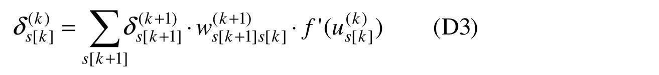

f’(us[k]
(k))は、活性化関数の導関数である。なお、数式(D3)の演算は、例えば、図6(B)に示す回路413によって実現できる。また、数式(D4)の演算は、例えば、図6(C)に示す回路414によって実現できる。出力関数の導関数は、例えば、オペアンプの出力端子に所望の導関数に対応した演算回路を接続することによって実現できる。
f'(us [k] (k) ) is the derivative of the activation function. The calculation of the mathematical formula (D3) can be realized by, for example, the
また、例えば、数式(D3)のΣδs[k+1]
(k+1)・ws[k+1]・s[k]
(k+1)の部分の演算は、後述する積和演算回路700によって実現できる。
Further, for example, the calculation of the Σδ s [k + 1] (k + 1) , w s [k + 1], s [k] (k + 1) portion of the mathematical formula (D3) can be realized by the multiply-accumulate
ここで、第(k+1)層が出力層のとき、すなわち、第(k+1)層が第L層であるとき、δs[L] (L)及び∂E/∂ws[L]s[L-1] (L)は、それぞれ次の式で表すことができる。 Here, when the first (k + 1) layer is the output layer, that is, when the first (k + 1) layer is the Lth layer, δ s [L] (L) and ∂E / ∂w s [L] s [L. -1] (L) can be expressed by the following equations, respectively.


数式(D5)の演算は、図6(D)に示す回路415によって実現できる。また、数式(D6)の演算は、図6(C)に示す回路414によって実現できる。
The calculation of the mathematical formula (D5) can be realized by the
つまり、数式(D1)乃至数式(D6)により、全てのニューロン回路の誤差δs[k] (k)及びδs[L] (L)を求めることができる。なお、重み係数の更新量は、誤差δs[k] (k)、δs[L] (L)及び所望のパラメータなどに基づいて、設定される。 That is, the errors δ s [k] (k) and δ s [L] (L) of all the neuron circuits can be obtained by the mathematical formulas (D1) to (D6). The update amount of the weighting coefficient is set based on the error δ s [k] (k) , δ s [L] (L) , a desired parameter, and the like.
以上のように、図6(A)乃至図6(D)に示す回路、及び後述する積和演算回路700を用いることによって、教師付き学習を適用した階層型ニューラルネットワークの計算を行うことができる。
As described above, by using the circuits shown in FIGS. 6 (A) to 6 (D) and the product-
<階層型ニューラルネットワークの構成例1>
次に、階層型ニューラルネットワークを構成する積和演算回路の例について、説明する。
<Structure example 1 of hierarchical neural network>
Next, an example of a product-sum calculation circuit constituting a hierarchical neural network will be described.
図7(A)に示す回路NNCは、列方向にM個及び行方向にN個のマトリクス状に配置されたM×N個(ここでのM、Nはそれぞれ1以上の整数である。)の積和演算回路を有する。なお、g行目(ここでのgは1以上M以下の整数である。)、h列目(ここでのhは1以上N以下の整数である。)に配置されている積和演算回路を、U[g,h]と記載している。なお、積和演算回路U[1,1]乃至積和演算回路U[M,N]はそれぞれ、列方向にm個及び行方向にn個のマトリクス状に配置されたm×n個(ここでのm、nはそれぞれ1以上の整数である。)のアナログメモリセルを有する。 The circuit NNC shown in FIG. 7A has M × N circuits arranged in a matrix of M in the column direction and N in the row direction (where M and N are integers of 1 or more, respectively). It has a product-sum calculation circuit. The product-sum operation circuit arranged in the g-th row (g here is an integer of 1 or more and M or less) and the h-th column (h here is an integer of 1 or more and N or less). Is described as U [g, h]. The product-sum calculation circuit U [1,1] to the product-sum calculation circuit U [M, N] are m × n arranged in a matrix of m in the column direction and n in the row direction, respectively (here). M and n in are integers of 1 or more, respectively.) Have analog memory cells.
積和演算回路U[g,h]は、後述する積和演算回路700とすることができる。また、積和演算回路U[g,h]は、後述するオフセット回路710を有さず、積和演算回路U[g,h]の外部でオフセット回路710と電気的に接続される構成にもすることができる。
The product-sum calculation circuit U [g, h] can be the product-
積和演算回路U[1,1]乃至積和演算回路U[M,N]のそれぞれは、端子RWと、端子WWと、端子WDと、端子Bと、を有する。端子RWは、後述する図11に示すメモリセルアレイ720における配線RW[1]乃至配線RW[m]と接続されるm個の端子である。同様に、端子WWは、メモリセルアレイ720における配線WW[1]乃至配線WW[m]と接続されるm個の端子であり、端子WDは、配線WD[1]乃至配線WD[n-1]及び配線WDrefと接続されるn個の端子であり、端子Bは、配線B[1]乃至配線B[n-1]及び配線Brefと接続されるn個の端子である。
Each of the product-sum calculation circuit U [1,1] to the product-sum calculation circuit U [M, N] has a terminal RW, a terminal WW, a terminal WD, and a terminal B. The terminals RW are m terminals connected to the wiring RW [1] to the wiring RW [m] in the
また、回路NNCは、配線群HRW[1]乃至配線群HRW[MN]と、配線群HWW[1]乃至配線群HWW[M]と、配線群VB[1]乃至配線群VB[NM]と、配線群VWD[1]乃至配線群VWD[N]と、を有している。なお、配線群HRW[1]乃至配線群HRW[MN]はそれぞれ、m本の配線であり、配線群HWW[1]乃至配線群HWW[M]はそれぞれ、m本の配線であり、配線群VB[1]乃至配線群VB[NM]はそれぞれ、n本の配線であり、配線群VWD[1]乃至配線群VWD[N]はそれぞれ、n本の配線である。 Further, the circuit NNC includes a wiring group HRW [1] to a wiring group HRW [MN], a wiring group HWW [1] to a wiring group HWW [M], and a wiring group VB [1] to a wiring group VB [NM]. , The wiring group VWD [1] to the wiring group VWD [N]. The wiring group HRW [1] to the wiring group HRW [MN] are each m wirings, and the wiring group HWW [1] to the wiring group HWW [M] are m wirings, respectively. Each of VB [1] to the wiring group VB [NM] has n wirings, and each of the wiring group VWD [1] to the wiring group VWD [N] has n wirings.
回路NNCは、複数のスイッチ回路MSWを有する。スイッチ回路MSWは、端子TV1と、端子TV2と、端子TH1と、端子TH2と、を有する。なお、端子TV1と端子TV2とは、電気的に接続状態となっており、端子TH1と端子TH2とは、電気的に接続状態となっている。 The circuit NNC has a plurality of switch circuits MSW. The switch circuit MSW has a terminal TV1, a terminal TV2, a terminal TH1, and a terminal TH2. The terminal TV1 and the terminal TV2 are electrically connected, and the terminal TH1 and the terminal TH2 are electrically connected.
スイッチ回路MSWは、端子TV1・端子TV2間と、端子TH1・端子TH2間と、を電気的に接続又は非接続のどちらかを選択する機能を有する。つまり、スイッチ回路MSWは、積和演算回路U[g,h]の端子と、配線と、を電気的に接続又は非接続のどちらかを選択する機能を有する。また、スイッチ回路MSWは、電気的に接続又は非接続のどちらかを決めるデータ(本明細書では、コンフィギュレーションデータという場合がある。)を保持する機能を有する。ここで、スイッチ回路MSWは、端子TV1・端子TV2間と、端子TH1・端子TH2間と、を電気的に接続又は非接続とするパストランジスタを有し、コンフィギュレーションデータによって、該パストランジスタの導通状態又は非導通状態を制御する構成であることが好ましい。 The switch circuit MSW has a function of selecting either electrically connected or unconnected between the terminal TV1 and the terminal TV2 and the terminal TH1 and the terminal TH2. That is, the switch circuit MSW has a function of electrically connecting or not connecting the terminal of the product-sum calculation circuit U [g, h] and the wiring. Further, the switch circuit MSW has a function of holding data (which may be referred to as configuration data in the present specification) that determines whether the switch circuit is electrically connected or disconnected. Here, the switch circuit MSW has a path transistor that electrically connects or disconnects the terminal TV1 and the terminal TV2 and the terminal TH1 and the terminal TH2, and the continuity of the path transistor is determined by the configuration data. It is preferable that the configuration controls the state or the non-conducting state.
なお、図7(A)では、積和演算回路U[1,1]、積和演算回路U[M,1]、積和演算回路U[1,N]、積和演算回路U[M,N]、配線群HRW[1]、配線群HRW[N]、配線群HRW[(M-1)N+1]、配線群HRW[MN]、配線群HWW[1]、配線群HWW[M]、配線群VB[1]、配線群VB[M]、配線群VB[(N-1)M+1]、配線群VB[NM]、配線群VWD[1]、配線群VWD[N]、端子RW、端子WW、端子WD、端子B、スイッチ回路MSW、端子TH1、端子TH2、端子TV1、端子TV2のみ図示し、他の積和演算回路については省略している。 In FIG. 7A, the product-sum calculation circuit U [1,1], the product-sum calculation circuit U [M, 1], the product-sum calculation circuit U [1, N], and the product-sum calculation circuit U [M, N], wiring group HRW [1], wiring group HRW [N], wiring group HRW [(M-1) N + 1], wiring group HRW [MN], wiring group HWW [1], wiring group HWW [M], Wiring group VB [1], Wiring group VB [M], Wiring group VB [(N-1) M + 1], Wiring group VB [NM], Wiring group VWD [1], Wiring group VWD [N], Terminal RW, Only the terminal WW, the terminal WD, the terminal B, the switch circuit MSW, the terminal TH1, the terminal TH2, the terminal TV1, and the terminal TV2 are shown, and the other product-sum calculation circuits are omitted.
なお、回路NNCの構成は、図7(A)に示した構成に限定されない。場合によって、又は、状況に応じて、回路NNCの構成から回路、配線、素子などを適宜除去してもよい。又は、回路NNCの構成に別の回路、配線、素子などを適宜追加してもよい。 The configuration of the circuit NNC is not limited to the configuration shown in FIG. 7A. In some cases, or depending on the situation, circuits, wirings, elements, etc. may be appropriately removed from the configuration of the circuit NNC. Alternatively, another circuit, wiring, element, or the like may be appropriately added to the configuration of the circuit NNC.
次に、積和演算回路U[1,1]乃至積和演算回路U[M,N]と、上述した配線と、複数のスイッチ回路MSWと、の接続構成について説明する。なお、簡易的に説明するため、図7(B)に示す積和演算回路U[g,h]に着目して、説明する。また、複数のスイッチ回路MSWについては、接続される配線ごとに、スイッチ回路MSW-RW、スイッチ回路MSW-WW、スイッチ回路MSW-B、及びスイッチ回路MSW-WDと、符号を付して、説明する。 Next, the connection configuration of the product-sum calculation circuit U [1,1] to the product-sum calculation circuit U [M, N], the above-mentioned wiring, and the plurality of switch circuits MSW will be described. For the sake of simplicity, the product-sum calculation circuit U [g, h] shown in FIG. 7B will be focused on. Further, the plurality of switch circuits MSW will be described by adding reference numerals to the switch circuit MSW-RW, the switch circuit MSW-WW, the switch circuit MSW-B, and the switch circuit MSW-WD for each connected wiring. do.
積和演算回路U[g,h]の端子RWは、N個のスイッチ回路MSW-RWと電気的に接続されている。N個のスイッチ回路MSW-RWのそれぞれは、配線群HRW[gN]乃至配線群HRW[(g-1)N+1]と電気的に接続されている。 The terminal RW of the product-sum calculation circuit U [g, h] is electrically connected to the N switch circuits MSW-RW. Each of the N switch circuits MSW-RW is electrically connected to the wiring group HRW [gN] to the wiring group HRW [(g-1) N + 1].
積和演算回路U[g,h]の端子WWは、スイッチ回路MSW-WWと電気的に接続されている。スイッチ回路MSW-WWは、配線群HWW[g]と電気的に接続されている。 The terminal WW of the product-sum calculation circuit U [g, h] is electrically connected to the switch circuit MSW-WW. The switch circuit MSW-WW is electrically connected to the wiring group HWW [g].
積和演算回路U[g,h]の端子Bは、M個のスイッチ回路MSW-Bと電気的に接続されている。M個のスイッチ回路MSW-Bのそれぞれは、配線群VB[(h-1)M+1]乃至配線群VB[hM]と電気的に接続されている。 The terminal B of the product-sum calculation circuit U [g, h] is electrically connected to the M switch circuits MSW-B. Each of the M switch circuits MSW-B is electrically connected to the wiring group VB [(h-1) M + 1] to the wiring group VB [hM].
積和演算回路U[g,h]の端子WDは、スイッチ回路MSW-WDと電気的に接続されている。スイッチ回路MSW-WDは、配線群VWD[h]と電気的に接続されている。 The terminal WD of the product-sum calculation circuit U [g, h] is electrically connected to the switch circuit MSW-WD. The switch circuit MSW-WD is electrically connected to the wiring group VWD [h].
<<スイッチ回路MSWの構成例1>>
スイッチ回路MSWの構成の一例を図8に示す。図8に示すスイッチ回路MSW1は、一方のx本の配線と、他方のx本の配線と、を電気的に接続する、又は非接続にする回路である。xは、1以上の整数であり、構成する配線の本数によって変更することができる。例えば、スイッチ回路MSW-RW、又はスイッチ回路MSW-WWに、スイッチ回路MSW1を用いる場合、xをnとして構成すればよい。また、例えば、スイッチ回路MSW-B、及びスイッチ回路MSW-WDに、スイッチ回路MSW1を用いる場合、xをmとして構成すればよい。
<< Configuration example 1 of switch circuit MSW >>
FIG. 8 shows an example of the configuration of the switch circuit MSW. The switch circuit MSW1 shown in FIG. 8 is a circuit that electrically connects or disconnects one x wiring and the other x wiring. x is an integer of 1 or more and can be changed depending on the number of wirings to be configured. For example, when the switch circuit MSW1 is used for the switch circuit MSW-RW or the switch circuit MSW-WW, x may be configured as n. Further, for example, when the switch circuit MSW1 is used for the switch circuit MSW-B and the switch circuit MSW-WD, x may be configured as m.
スイッチ回路MSW1は、端子TV1と、端子TV2と、端子TH1と、端子TH2と、を有する。端子TV1は、端子TV1[1]乃至端子TV1[x]を有し、端子TV2は、端子TV2[1]乃至端子TV2[x]を有し、端子TH1は、端子TH1[1]乃至端子TH1[x]を有し、端子TH2は、端子TH2[1]乃至端子TH2[x]を有する。 The switch circuit MSW1 has a terminal TV1, a terminal TV2, a terminal TH1, and a terminal TH2. The terminal TV1 has the terminal TV1 [1] to the terminal TV1 [x], the terminal TV2 has the terminal TV2 [1] to the terminal TV2 [x], and the terminal TH1 has the terminal TH1 [1] to the terminal TH1. It has [x], and the terminal TH2 has a terminal TH2 [1] to a terminal TH2 [x].
端子TV1[x0](x0は1以上x以下の整数である。)は、端子TV2[x0]と電気的に接続され、端子TH1[x0]は、端子TH2[x0]と電気的に接続されている。なお、図8では、端子TV1[x0]、端子TV2[x0]、端子TH1[x0]、及び端子TH2[x0]の記載を省略している。 The terminal TV 1 [x 0 ] (x 0 is an integer of 1 or more and x or less) is electrically connected to the terminal TV 2 [x 0 ], and the terminal TH1 [x 0 ] is connected to the terminal TH2 [x 0 ]. It is electrically connected. In FIG. 8, the description of the terminal TV1 [x 0 ], the terminal TV2 [x 0 ], the terminal TH1 [x 0 ], and the terminal TH2 [x 0 ] is omitted.
スイッチ回路MSW1は、回路SW[1]乃至回路SW[x]を有する。回路SW[1]乃至回路SW[x]のそれぞれは、トランジスタTr31と、トランジスタTr32と、容量素子C4と、を有する。 The switch circuit MSW1 has a circuit SW [1] to a circuit SW [x]. Each of the circuit SW [1] to the circuit SW [x] has a transistor Tr31, a transistor Tr32, and a capacitive element C4.
ここで、回路SW[1]乃至回路SW[x]の内部の構成について、回路SW[x0]に着目して、説明する。トランジスタTr31の第1端子は、配線SWB[x0]と電気的に接続され、トランジスタTr31の第2端子は、容量素子C4の第1端子と電気的に接続され、トランジスタTr31のゲートは、配線SWW[x0]と電気的に接続されている。トランジスタTr32の第1端子は、端子TV1[x0]及び端子TV2[x0]と電気的に接続され、トランジスタTr32の第2端子は、端子TH1[x0]及び端子TH2[x0]と電気的に接続され、トランジスタTr32のゲートは、容量素子C4の第1端子と電気的に接続されている。容量素子C4の第2端子は、配線VSSLと電気的に接続されている。なお、トランジスタTr31の第2端子と、容量素子C4の第1端子と、トランジスタTr32のゲートと、の接続箇所を、回路SW[x0]における保持ノードとする。 Here, the internal configuration of the circuit SW [1] to the circuit SW [x] will be described with a focus on the circuit SW [x 0 ]. The first terminal of the transistor Tr31 is electrically connected to the wiring SWB [x 0 ], the second terminal of the transistor Tr31 is electrically connected to the first terminal of the capacitive element C4, and the gate of the transistor Tr31 is wired. It is electrically connected to SWW [x 0 ]. The first terminal of the transistor Tr32 is electrically connected to the terminal TV1 [x 0 ] and the terminal TV2 [x 0 ], and the second terminal of the transistor Tr32 is connected to the terminal TH1 [x 0 ] and the terminal TH2 [x 0 ]. It is electrically connected, and the gate of the transistor Tr32 is electrically connected to the first terminal of the capacitive element C4. The second terminal of the capacitive element C4 is electrically connected to the wiring VSSL. The connection point between the second terminal of the transistor Tr31, the first terminal of the capacitive element C4, and the gate of the transistor Tr32 is a holding node in the circuit SW [x 0 ].
配線SWW[x0]は、回路SW[x0]に対して、選択信号を供給する配線であり、配線SWB[x0]は、回路SW[x0]にコンフィギュレーションデータを供給するための配線である。配線SWW[x0]から高レベル電位を入力することにより、回路SW[x0]のトランジスタTr31のゲートに高レベル電位が印加されるため、トランジスタTr31は導通状態となる。このとき、配線SWB[x0]からコンフィギュレーションデータに応じた電位を供給することによって、保持ノードに該電位が書き込まれる。その後、配線SWW[x0]から低レベル電位を入力して、トランジスタTr31を非導通状態にすることによって、該電位を保持することができる。該電位は、トランジスタTr32のゲートに印加されているため、トランジスタTr32は、コンフィギュレーションデータに応じて、導通状態又は非導通状態のどちらかに決まる。 The wiring SWW [x 0 ] is a wiring for supplying a selection signal to the circuit SW [x 0 ], and the wiring SWB [x 0 ] is for supplying configuration data to the circuit SW [x 0 ]. Wiring. By inputting a high level potential from the wiring SWW [x 0 ], the high level potential is applied to the gate of the transistor Tr 31 of the circuit SW [x 0 ], so that the transistor Tr 31 is in a conductive state. At this time, the potential is written to the holding node by supplying the potential according to the configuration data from the wiring SWB [x 0 ]. After that, a low level potential is input from the wiring SWW [x 0 ] to bring the transistor Tr31 into a non-conducting state, so that the potential can be maintained. Since the potential is applied to the gate of the transistor Tr32, the transistor Tr32 is determined to be in a conducting state or a non-conducting state depending on the configuration data.
なお、図8では、配線SWW[1]乃至配線SWW[x]と表記しているが、図8の構成に限定しなくてもよい。例えば、配線SWW[1]乃至配線SWW[x]を一本の配線にまとめることで、回路SW[1]乃至回路SW[x]を一括に選択することができる。これにより、回路SW[1]乃至回路SW[x]に対して、同時にコンフィギュレーションデータを書き込むことができる。 Although it is described as wiring SWW [1] to wiring SWW [x] in FIG. 8, it does not have to be limited to the configuration of FIG. For example, by combining the wiring SWW [1] to the wiring SWW [x] into one wiring, the circuit SW [1] to the circuit SW [x] can be collectively selected. As a result, configuration data can be written to the circuit SW [1] to the circuit SW [x] at the same time.
また、図8では、配線SWB[1]乃至配線SWB[x]と表記しているが、図8の構成に限定しなくてもよい。例えば、配線SWB[1]乃至配線SWB[x]を一本の配線にまとめることで、スイッチ回路MSW1の回路面積を低減することができる。この場合、配線SWW[1]乃至配線SWW[x]によって、回路SW[1]乃至回路SW[x]を順次選択していき、選択されたときに所定のコンフィギュレーションデータを書き込む動作を行えばよい。 Further, in FIG. 8, the wiring SWB [1] to the wiring SWB [x] are described, but the configuration is not limited to that shown in FIG. For example, by combining the wiring SWB [1] to the wiring SWB [x] into one wiring, the circuit area of the switch circuit MSW1 can be reduced. In this case, the circuit SW [1] to the circuit SW [x] are sequentially selected by the wiring SWW [1] to the wiring SWW [x], and when the circuit SW [1] to the circuit SW [x] is selected, the operation of writing the predetermined configuration data is performed. good.
なお、図8のスイッチ回路MSW1では、回路SW[1]、回路SW[x]、配線SWW[1]、配線SWW[x]、配線SWB[1]、配線SWB[x]、配線VSSL、端子TV1、端子TV1[1]、端子TV1[x]、端子TV2、端子TV2[1]、端子TV2[x]、端子TH1、端子TH1[1]、端子TH1[x]、端子TH2、端子TH2[1]、端子TH2[x]、トランジスタTr31、トランジスタTr32、容量素子C4のみ図示しており、それ以外の配線、回路、素子、及びこれらの符号については省略している。 In the switch circuit MSW1 of FIG. 8, the circuit SW [1], the circuit SW [x], the wiring SWW [1], the wiring SWW [x], the wiring SWB [1], the wiring SWB [x], the wiring VSSL, and the terminal. TV1, terminal TV1 [1], terminal TV1 [x], terminal TV2, terminal TV2 [1], terminal TV2 [x], terminal TH1, terminal TH1 [1], terminal TH1 [x], terminal TH2, terminal TH2 [ 1], terminal TH2 [x], transistor Tr31, transistor Tr32, and capacitive element C4 are shown only, and other wiring, circuits, elements, and symbols thereof are omitted.
<<スイッチ回路MSWの構成例2>>
スイッチ回路MSWの構成について、図8とは別の一例を図9に示す。図9に示すスイッチ回路MSW2は、スイッチ回路MSW1と同様に、一方のx本の配線と、他方のx本の配線と、を電気的に接続する、又は非接続にする回路である。xは構成する配線の本数によって変更することができる。
<< Configuration example 2 of switch circuit MSW >>
FIG. 9 shows an example of the configuration of the switch circuit MSW, which is different from that of FIG. Similar to the switch circuit MSW1, the switch circuit MSW2 shown in FIG. 9 is a circuit that electrically connects or disconnects one x wiring and the other x wiring. x can be changed depending on the number of wirings to be configured.
スイッチ回路MSW2は、端子TV1と、端子TV2と、端子TH1と、端子TH2と、を有する。端子TV1は、端子TV1[1]乃至端子TV1[x]を有し、端子TV2は、端子TV2[1]乃至端子TV2[x]を有し、端子TH1は、端子TH1[1]乃至端子TH1[x]を有し、端子TH2は、端子TH2[1]乃至端子TH2[x]を有する。 The switch circuit MSW2 has a terminal TV1, a terminal TV2, a terminal TH1, and a terminal TH2. The terminal TV1 has the terminal TV1 [1] to the terminal TV1 [x], the terminal TV2 has the terminal TV2 [1] to the terminal TV2 [x], and the terminal TH1 has the terminal TH1 [1] to the terminal TH1. It has [x], and the terminal TH2 has a terminal TH2 [1] to a terminal TH2 [x].
端子TV1[x0]は、端子TV2[x0]と電気的に接続され、端子TH1[x0]は、端子TH2[x0]と電気的に接続されている。なお、図9では、端子TV1[x0]、端子TV2[x0]、端子TH1[x0]、及び端子TH2[x0]の記載を省略している。 The terminal TV1 [x 0 ] is electrically connected to the terminal TV2 [x 0 ], and the terminal TH1 [x 0 ] is electrically connected to the terminal TH2 [x 0 ]. In FIG. 9, the description of the terminal TV1 [x 0 ], the terminal TV2 [x 0 ], the terminal TH1 [x 0 ], and the terminal TH2 [x 0 ] is omitted.
スイッチ回路MSW2は、トランジスタTr41と、トランジスタTr42[1]乃至トランジスタTr42[x]と、容量素子C5と、を有する。 The switch circuit MSW2 includes a transistor Tr41, a transistor Tr42 [1] to a transistor Tr42 [x], and a capacitive element C5.
ここで、スイッチ回路MSW2の内部の構成について、説明する。トランジスタTr41の第1端子は、配線SWBと電気的に接続され、トランジスタTr41の第2端子は、トランジスタTr42[1]乃至トランジスタTr42[x]のそれぞれのゲートと電気的に接続され、トランジスタTr41のゲートは、配線SWWと電気的に接続されている。トランジスタTr42[x0]の第1端子は、端子TV1[x0]及び端子TV2[x0]と電気的に接続され、トランジスタTr42[x0]の第2端子は、端子TH1[x0]及び端子TH2[x0]と電気的に接続されている。容量素子C5の第1端子は、トランジスタTr41の第2端子と電気的に接続され、容量素子C5の第1端子は、配線VSSLと電気的に接続されている。なお、トランジスタTr41の第2端子と、容量素子C4の第1端子と、トランジスタTr42[1]乃至トランジスタTr42[x]のゲートと、の接続箇所を、スイッチ回路MSW2における保持ノードとする。 Here, the internal configuration of the switch circuit MSW2 will be described. The first terminal of the transistor Tr41 is electrically connected to the wiring SWB, and the second terminal of the transistor Tr41 is electrically connected to the respective gates of the transistor Tr42 [1] to the transistor Tr42 [x]. The gate is electrically connected to the wiring SWW. The first terminal of the transistor Tr42 [x 0 ] is electrically connected to the terminal TV1 [x 0 ] and the terminal TV2 [x 0 ], and the second terminal of the transistor Tr42 [x 0 ] is the terminal TH1 [x 0 ]. And is electrically connected to the terminal TH2 [x 0 ]. The first terminal of the capacitive element C5 is electrically connected to the second terminal of the transistor Tr41, and the first terminal of the capacitive element C5 is electrically connected to the wiring VSSL. The connection point between the second terminal of the transistor Tr41, the first terminal of the capacitive element C4, and the gate of the transistor Tr42 [1] to the transistor Tr42 [x] is a holding node in the switch circuit MSW2.
配線SWWは、スイッチ回路MSW2のトランジスタTr41のゲートに電位を与える配線であり、配線SWBは、スイッチ回路MSW2にコンフィギュレーションデータを供給するための配線である。配線SWWから高レベル電位を入力することにより、トランジスタTr41のゲートに高レベル電位が印加されるため、トランジスタTr41は導通状態となる。このとき、配線SWBからコンフィギュレーションデータに応じた電位を供給することによって、保持ノードに該電位が書き込まれる。その後、配線SWWから低レベル電位を入力して、トランジスタTr41を非導通状態にすることによって、該電位を保持することができる。該電位は、トランジスタTr42[1]乃至トランジスタTr42[x]のそれぞれのゲートに印加されているため、トランジスタTr42[1]乃至トランジスタTr42[x]のそれぞれは、コンフィギュレーションデータに応じて、導通状態又は非導通状態のどちらか同時に決まる。 The wiring SWW is a wiring that gives a potential to the gate of the transistor Tr41 of the switch circuit MSW2, and the wiring SWB is a wiring for supplying configuration data to the switch circuit MSW2. By inputting the high level potential from the wiring SWW, the high level potential is applied to the gate of the transistor Tr41, so that the transistor Tr41 is in a conductive state. At this time, the potential is written to the holding node by supplying the potential according to the configuration data from the wiring SWB. After that, a low level potential is input from the wiring SWW to bring the transistor Tr41 into a non-conducting state, so that the potential can be maintained. Since the potential is applied to the respective gates of the transistor Tr42 [1] to the transistor Tr42 [x], each of the transistor Tr42 [1] to the transistor Tr42 [x] is in a conduction state according to the configuration data. Either the non-conducting state or the non-conducting state is determined at the same time.
なお、図9のスイッチ回路MSW2では、配線SWW、配線SWB、配線VSSL、端子TV1、端子TV1[1]、端子TV1[x]、端子TV2、端子TV2[1]、端子TV2[x]、端子TH1、端子TH1[1]、端子TH1[x]、端子TH2、端子TH2[1]、端子TH2[x]、トランジスタTr41、トランジスタTr42[1]、トランジスタTr42[x]、容量素子C5のみ図示しており、それ以外の配線、回路、素子、及びこれらの符号については省略している。 In the switch circuit MSW2 of FIG. 9, the wiring SWW, the wiring SWB, the wiring VSSL, the terminal TV1, the terminal TV1 [1], the terminal TV1 [x], the terminal TV2, the terminal TV2 [1], the terminal TV2 [x], and the terminal. TH1, terminal TH1 [1], terminal TH1 [x], terminal TH2, terminal TH2 [1], terminal TH2 [x], transistor Tr41, transistor Tr42 [1], transistor Tr42 [x], and capacitive element C5 only are shown. Other wiring, circuits, elements, and their codes are omitted.
また、トランジスタTr31、トランジスタTr32、トランジスタTr41、及びトランジスタTr42[1]乃至トランジスタTr42[x]として、OSトランジスタを用いることにより、トランジスタTr31、トランジスタTr32、トランジスタTr41、及びトランジスタTr42[1]乃至トランジスタTr42[x]のそれぞれのリーク電流を抑えることができるため、精度の高い積和演算回路を実現できる場合がある。また、トランジスタTr31、又はトランジスタTr41として、OSトランジスタを用いることにより、トランジスタTr31、又はトランジスタTr41が非導通状態における、保持ノードから配線SWB[1]乃至配線SWB[x]のいずれかへのリーク電流を非常に小さくすることができる。つまり、保持ノードの電位のリフレッシュ動作を少なくすることができるため、積和演算回路を有する半導体装置の消費電力を低減することができる。特に、OSトランジスタに用いる酸化物半導体は、実施の形態9で説明するCAC-OSを用いるのが好ましい。 Further, by using an OS transistor as the transistor Tr31, the transistor Tr32, the transistor Tr41, and the transistor Tr42 [1] to the transistor Tr42 [x], the transistor Tr31, the transistor Tr32, the transistor Tr41, and the transistor Tr42 [1] to the transistor Tr42 Since the leakage current of each of [x] can be suppressed, a product-sum calculation circuit with high accuracy may be realized. Further, by using an OS transistor as the transistor Tr31 or the transistor Tr41, the leakage current from the holding node to any of the wiring SWB [1] to the wiring SWB [x] when the transistor Tr31 or the transistor Tr41 is in a non-conducting state. Can be made very small. That is, since the potential refreshing operation of the holding node can be reduced, the power consumption of the semiconductor device having the product-sum calculation circuit can be reduced. In particular, as the oxide semiconductor used for the OS transistor, it is preferable to use CAC-OS described in the ninth embodiment.
また、図8では、トランジスタTr32として、nチャネル型のトランジスタを図示しているが、代わりにpチャネル型のトランジスタとしてもよい。同様に、図9では、トランジスタTr42[1]乃至トランジスタTr42[x]として、nチャネル型のトランジスタを図示しているが、代わりにpチャネル型のトランジスタとしてもよい。 Further, in FIG. 8, the n-channel type transistor is shown as the transistor Tr32, but a p-channel type transistor may be used instead. Similarly, in FIG. 9, the n-channel type transistor is shown as the transistor Tr42 [1] to the transistor Tr42 [x], but a p-channel type transistor may be used instead.
<階層型ニューラルネットワークの構成例2>
図7(A)に示した回路NNCの具体的な一例を図10に示す。
<Structure example 2 of hierarchical neural network>
A specific example of the circuit NNC shown in FIG. 7 (A) is shown in FIG.
図10の回路NNCは、積和演算回路U[1,1]と、積和演算回路U[1,2]と、積和演算回路U[1,3]と、積和演算回路U[2,1]と、積和演算回路U[2,2]と、積和演算回路U[2,3]と、積和演算回路U[3,1]と、積和演算回路U[3,2]と、積和演算回路U[3,3]と、を有する。つまり、図10の回路NNCは、図7(A)の回路NNCにおいてMを3とし、かつNを3とした構成となっている。 The circuit NNC of FIG. 10 includes a product-sum calculation circuit U [1,1], a product-sum calculation circuit U [1,2], a product-sum calculation circuit U [1,3], and a product-sum calculation circuit U [2]. , 1], the product-sum calculation circuit U [2,2], the product-sum calculation circuit U [2,3], the product-sum calculation circuit U [3,1], and the product-sum calculation circuit U [3,2]. ] And the product-sum calculation circuit U [3,3]. That is, the circuit NNC of FIG. 10 has a configuration in which M is 3 and N is 3 in the circuit NNC of FIG. 7 (A).
ところで、図10の回路NNCの配線については、Mを3とし、かつNを3とした図7(A)の回路NNCの構成から、配線群HRW[3]、配線群HRW[6]、配線群HRW[9]、配線群VB[3]、配線群VB[6]、及び配線群VB[9]を除去している。つまり、図10の回路NNCは、配線群HRW[1]、配線群HRW[2]、配線群HRW[4]、配線群HRW[5]、配線群HRW[7]、配線群HRW[8]、配線群HWW[1]、配線群HWW[2]、配線群HWW[3]、配線群VB[1]、配線群VB[2]、配線群VB[4]、配線群VB[5]、配線群VB[7]、配線群VB[8]、配線群VWD[1]、配線群VWD[2]、及び配線群VWD[3]を有する。 By the way, regarding the wiring of the circuit NNC of FIG. 10, from the configuration of the circuit NNC of FIG. 7A in which M is 3 and N is 3, the wiring group HRW [3], the wiring group HRW [6], and the wiring The group HRW [9], the wiring group VB [3], the wiring group VB [6], and the wiring group VB [9] are removed. That is, in the circuit NNC of FIG. 10, the wiring group HRW [1], the wiring group HRW [2], the wiring group HRW [4], the wiring group HRW [5], the wiring group HRW [7], and the wiring group HRW [8]. , Wiring group HWW [1], Wiring group HWW [2], Wiring group HWW [3], Wiring group VB [1], Wiring group VB [2], Wiring group VB [4], Wiring group VB [5], It has a wiring group VB [7], a wiring group VB [8], a wiring group VWD [1], a wiring group VWD [2], and a wiring group VWD [3].
積和演算回路U[1,1]乃至積和演算回路U[3,3]のそれぞれが有するメモリセルアレイ720は、n2個のメモリセルAMを有する。また、メモリセルAMは、積和演算回路U[1,1]乃至積和演算回路U[3,3]のそれぞれのメモリセルアレイ720において、列方向にn個、行方向にn個のマトリクス状に設けられている。
The
配線群HRW[1]、配線群HRW[2]、配線群HRW[4]、配線群HRW[5]、配線群HRW[7]、配線群HRW[8]、配線群HWW[1]乃至配線群HWW[3]、配線群VB[1]、配線群VB[2]、配線群VB[4]、配線群VB[5]、配線群VB[7]、配線群VB[8]、及び配線群VWD[1]乃至配線群VWD[3]は、それぞれn本の配線である。また、配線群HRW[1]、配線群HRW[2]、配線群HRW[4]、配線群HRW[5]、配線群HRW[7]、配線群HRW[8]、及び配線群HWW[1]乃至配線群HWW[3]のそれぞれは、各々のスイッチ回路MSW2を介して、積和演算回路の端子RW、又は端子WWと、に電気的に接続されている。同様に、配線群VB[1]、配線群VB[2]、配線群VB[4]、配線群VB[5]、配線群VB[7]、配線群VB[8]、及び配線群VWD[1]乃至配線群VWD[3]のそれぞれは、各々のスイッチ回路MSW2を介して、積和演算回路の端子WD、又は端子Bと、に電気的に接続されている。 Wiring group HRW [1], wiring group HRW [2], wiring group HRW [4], wiring group HRW [5], wiring group HRW [7], wiring group HRW [8], wiring group HWW [1] to wiring Group HWW [3], wiring group VB [1], wiring group VB [2], wiring group VB [4], wiring group VB [5], wiring group VB [7], wiring group VB [8], and wiring. The group VWD [1] to the wiring group VWD [3] are each n wirings. Further, the wiring group HRW [1], the wiring group HRW [2], the wiring group HRW [4], the wiring group HRW [5], the wiring group HRW [7], the wiring group HRW [8], and the wiring group HWW [1]. ] To Each of the wiring groups HWW [3] is electrically connected to the terminal RW or the terminal WW of the product-sum calculation circuit via the respective switch circuit MSW2. Similarly, the wiring group VB [1], the wiring group VB [2], the wiring group VB [4], the wiring group VB [5], the wiring group VB [7], the wiring group VB [8], and the wiring group VWD [ Each of 1] to the wiring group VWD [3] is electrically connected to the terminal WD or the terminal B of the product-sum calculation circuit via the respective switch circuit MSW2.
なお、スイッチ回路MSW2の詳細については、前述の階層型ニューラルネットワークの構成例1のとおりである。そのため、スイッチ回路MSW2の保持ノードに高レベル電位が印加されているとき、そのスイッチ回路MSW2を介して接続される配線と端子とは、電気的に導通となり、スイッチ回路MSW2の保持ノードに低レベル電位が印加されているとき、そのスイッチ回路MSW2を介して接続される配線と端子とは、電気的に非導通となる。図10では、導通状態となるスイッチ回路MSW2を黒い正方形として図示し、非導通状態となるスイッチ回路MSW2を白い正方形として図示し、回路NNCの動作中に導通状態、又は非導通状態の切り替えが行われるスイッチ回路MSW2を黒い正三角形として図示している。なお、スイッチ回路MSW2の代わりに、スイッチ回路MSW1を用いてもよい。 The details of the switch circuit MSW2 are as described in Configuration Example 1 of the above-mentioned hierarchical neural network. Therefore, when a high level potential is applied to the holding node of the switch circuit MSW2, the wiring and the terminal connected via the switch circuit MSW2 become electrically conductive, and the holding node of the switch circuit MSW2 has a low level. When a potential is applied, the wiring and terminals connected via the switch circuit MSW2 are electrically non-conducting. In FIG. 10, the switch circuit MSW2 in the conductive state is shown as a black square, the switch circuit MSW2 in the non-conducting state is shown as a white square, and the switching between the conductive state and the non-conducting state is performed during the operation of the circuit NNC. The switch circuit MSW2 is illustrated as a black equilateral triangle. The switch circuit MSW1 may be used instead of the switch circuit MSW2.
図10の回路NNCでは、入力層(第1層)は、2n個のニューロンを有し、第1隠れ層(第2層)は、2n個のニューロンを有し、第2隠れ層(第3層)は、n個のニューロンを有し、出力層(第4層)は、3n個のニューロンを有する場合を示している。 In the circuit NNC of FIG. 10, the input layer (first layer) has 2n neurons, the first hidden layer (second layer) has 2n neurons, and the second hidden layer (third layer). The layer) has n neurons, and the output layer (fourth layer) has 3n neurons.
積和演算回路U[1,1]、積和演算回路U[1,2]、積和演算回路U[2,1]、積和演算回路U[2,2]のメモリセルAMには、第1隠れ層のニューロンへの入力に対する重み係数W(2)が格納される。また、積和演算回路U[1,3]、積和演算回路U[2,3]、のメモリセルAMには第2隠れ層のニューロンへの入力に対する重み係数W(3)が格納されている。更に、積和演算回路U[3,1]、積和演算回路U[3,2]、積和演算回路U[3,3]のメモリセルAMには、出力層のニューロンへの入力に対する重み係数W(4)が格納される。なお、配線群HWW[1]乃至配線群HWW[3]は、配線WW(3n本の信号線)に対応し、配線群VWD[1]乃至配線群VWD[3]は、配線WD(3n本の信号線)に対応する。配線WWに選択信号WWSigを順次送信し、配線WDに選択信号WWSigに対応するデータ(図10ではWと表記する。)を供給することで、それぞれの積和演算回路のメモリセルAMのそれぞれに、重み係数を格納することができる。 The memory cell AM of the product-sum calculation circuit U [1,1], the product-sum calculation circuit U [1,2], the product-sum calculation circuit U [2,1], and the product-sum calculation circuit U [2,2] The weighting coefficient W (2) for the input to the neurons of the first hidden layer is stored. Further, the weight coefficient W (3) for the input to the neuron of the second hidden layer is stored in the memory cell AM of the product-sum calculation circuit U [1,3] and the product-sum calculation circuit U [2,3]. There is. Further, the memory cell AM of the product-sum calculation circuit U [3,1], the product-sum calculation circuit U [3,2], and the product-sum calculation circuit U [3,3] has a weight for the input of the output layer to the neuron. The coefficient W (4) is stored. The wiring group HWW [1] to the wiring group HWW [3] correspond to the wiring WW (3n signal lines), and the wiring group VWD [1] to the wiring group VWD [3] correspond to the wiring WD (3n lines). Corresponds to the signal line). By sequentially transmitting the selection signal WWSig to the wiring WW and supplying the data corresponding to the selection signal WWSig (referred to as W in FIG. 10) to the wiring WD, each of the memory cells AM of each product-sum calculation circuit is supplied with data. , Weight factor can be stored.
第1隠れ層への信号の入力と、第1隠れ層からの信号の出力と、について説明する。入力層の2n個のニューロンの出力は、2n個の信号RWSig(2)として、配線群HRW[1]及び配線群HRW[4]の計2n本の信号線を介して、積和演算回路U[1,1]と、積和演算回路U[1,2]と、積和演算回路U[2,1]と、積和演算回路U[2,2]と、に格納される。積和演算回路U[1,1]と、積和演算回路U[1,2]と、積和演算回路U[2,1]と、積和演算回路U[2,2]と、の出力は、2n個の信号BSig(2)として、配線群VB[1]及び配線群VB[4]の計2n本の信号線を介して、出力される。つまり、2n個の信号BSig(2)のそれぞれが、入力層から入力された信号と、重み係数W(2)と、の積和演算された値となり、第1隠れ層への入力の総和(ネット値ともいう。)に相当する。そして、2n個の信号BSig(2)が、配線群VB[1]及び配線群VB[4]から出力された後に、積和演算された値から活性化関数の値を求めて、第1隠れ層から出力されるニューロン信号を生成することができる。 The input of the signal to the first hidden layer and the output of the signal from the first hidden layer will be described. The output of the 2n neurons in the input layer is the product-sum calculation circuit U as 2n signals RWSig (2) via a total of 2n signal lines of the wiring group HRW [1] and the wiring group HRW [4]. It is stored in [1,1], the product-sum calculation circuit U [1,2], the product-sum calculation circuit U [2,1], and the product-sum calculation circuit U [2,2]. Outputs of the product-sum calculation circuit U [1,1], the product-sum calculation circuit U [1,2], the product-sum calculation circuit U [2,1], and the product-sum calculation circuit U [2,2]. Is output as 2n signals BSig (2) via a total of 2n signal lines of the wiring group VB [1] and the wiring group VB [4]. That is, each of the 2n signals BSig (2) is a value calculated by multiplying the signal input from the input layer and the weighting coefficient W (2), and is the sum of the inputs to the first hidden layer (the sum of the inputs to the first hidden layer). It is also called a net value.) Then, after the 2n signals BSig (2) are output from the wiring group VB [1] and the wiring group VB [4], the value of the activation function is obtained from the value calculated by the product sum, and the first hidden function is obtained. It is possible to generate a neuron signal output from the layer.
第2隠れ層への信号の入力と、第2隠れ層からの信号の出力と、について説明する。第1隠れ層の2n個のニューロンの出力は、2n個の信号RWSig(3)として、配線群HRW[2]及び配線群HRW[5]の計2n本の信号線を介して、積和演算回路U[1,3]と、積和演算回路U[2,3]と、に格納される。積和演算回路U[1,3]と、積和演算回路U[2,3]と、の出力は、n個の信号BSig(3)として、配線群VB[7]の計n本の信号線を介して、出力される。つまり、n個の信号BSig(3)のそれぞれが、入力層から入力された信号と、重み係数W(3)と、の積和演算された値となり、第2隠れ層への入力の総和に相当する。そして、n個の信号BSig(3)が、配線群VB[7]から出力された後に、積和演算された値から活性化関数の値を求めて、第2隠れ層から出力されるニューロン信号を生成することができる。 The input of the signal to the second hidden layer and the output of the signal from the second hidden layer will be described. The output of the 2n neurons in the first hidden layer is a product-sum calculation as 2n signals RWSig (3) via a total of 2n signal lines of the wiring group HRW [2] and the wiring group HRW [5]. It is stored in the circuit U [1,3] and the product-sum calculation circuit U [2,3]. The outputs of the product-sum calculation circuit U [1,3] and the product-sum calculation circuit U [2,3] are n signals BSig (3), and a total of n signals of the wiring group VB [7]. It is output via a line. That is, each of the n signals BSig (3) is a value calculated by multiplying the signal input from the input layer and the weighting coefficient W (3), and is the sum of the inputs to the second hidden layer. Equivalent to. Then, after n signals BSig (3) are output from the wiring group VB [7], the value of the activation function is obtained from the value calculated by multiply-accumulate, and the neuron signal output from the second hidden layer. Can be generated.
出力層への信号の入力と、出力層からの信号の出力と、について説明する。第2隠れ層のn個のニューロンの出力は、n個の信号RWSig(4)として、配線群HRW[8]の計n本の信号線を介して、積和演算回路U[3,1]と、積和演算回路U[3,2]と、積和演算回路U[3,3]と、に格納される。積和演算回路U[3,1]と、積和演算回路U[3,2]と、積和演算回路U[3,3]と、の出力は、3n個の信号BSig(4)として、配線群VB[2]と、配線群VB[5]と、配線群VB[8]と、の計3n本の信号線を介して、出力される。つまり、3n個の信号BSig(4)のそれぞれが、入力層から入力された信号と、重み係数W(4)と、の積和演算された値となり、出力層への入力の総和に相当する。そして、3n個の信号BSig(4)が、配線群VB[2]と、配線群VB[5]と、配線群VB[8]と、から出力された後に、積和演算された値から活性化関数の値を求めて、出力層から出力されるニューロン信号を生成することができる。 The input of the signal to the output layer and the output of the signal from the output layer will be described. The output of n neurons in the second hidden layer is the product-sum calculation circuit U [3,1] via a total of n signal lines of the wiring group HRW [8] as n signals RWSig (4). , And the product-sum calculation circuit U [3,2] and the product-sum calculation circuit U [3,3]. The outputs of the product-sum calculation circuit U [3,1], the product-sum calculation circuit U [3,2], and the product-sum calculation circuit U [3,3] are as 3n signals BSig (4). It is output via a total of 3n signal lines of the wiring group VB [2], the wiring group VB [5], and the wiring group VB [8]. That is, each of the 3n signals BSig (4) is a value calculated by multiplying the signal input from the input layer and the weighting coefficient W (4), and corresponds to the total sum of the inputs to the output layer. .. Then, after the 3n signals BSig (4) are output from the wiring group VB [2], the wiring group VB [5], and the wiring group VB [8], they are activated from the value calculated by the product sum. The value of the conversion function can be obtained to generate the neuron signal output from the output layer.
以上のように、複数の配線と、複数の積和演算回路と、の間に、互いを接続する又は非接続にするスイッチを設けることにより、階層型ニューラルネットワークの回路の接続を自由に変更することができる。これにより、積和演算処理を小さな回路規模で高速で駆動でき、かつ低消費電力で駆動できる半導体装置を実現できる。 As described above, the connection of the circuit of the hierarchical neural network can be freely changed by providing a switch for connecting or disconnecting each other between the plurality of wirings and the plurality of multiply-accumulate circuits. be able to. As a result, it is possible to realize a semiconductor device that can drive the product-sum calculation process at high speed on a small circuit scale and can be driven with low power consumption.
<積和演算回路の構成例>
次に、上述した階層型ニューラルネットワークを実現するための積和演算回路の構成例について、説明する。
<Configuration example of product-sum calculation circuit>
Next, a configuration example of a product-sum calculation circuit for realizing the above-mentioned hierarchical neural network will be described.
図11に積和演算処理が可能な回路の一例を示す。図11は、積和演算回路のブロック図を示しており、積和演算回路700は、オフセット回路710と、メモリセルアレイ720と、を有する。
FIG. 11 shows an example of a circuit capable of multiply-accumulate operation processing. FIG. 11 shows a block diagram of a product-sum calculation circuit, and the product-
オフセット回路710は、列出力回路OUT[1]乃至列出力回路OUT[n](ここでのnは1以上の整数である。)と、参照列出力回路Crefと、を有する。
The offset
メモリセルアレイ720は、列方向にm個(ここでのmは1以上の整数である。)、行方向にn個、合計m×n個のメモリセルAMと、列方向にm個のメモリセルAMrefと、を有する。メモリセルAMと、メモリセルAMrefと、は、メモリセルアレイ720において、m×(n+1)のマトリクス状に設けられている。特に、図11のメモリセルアレイ720では、i行目j列目に位置するメモリセルAMを、メモリセルAM[i,j](iは1以上m以下の整数であり、jは1以上n以下の整数である。)と表記し、i行目に位置するメモリセルAMrefを、メモリセルAMref[i]と表記する。
The
なお、上述の階層型ニューラルネットワークの構成例1において、積和演算回路が有するメモリセルアレイは、列方向にm個及び行方向にn個のマトリクス状に配置されたm×n個のアナログメモリセルを有する、と説明したが、本構成例で説明する積和演算回路が有するメモリセルアレイは、上述のとおり、列方向にm個及び行方向に(n+1)個のマトリクス状に配置されたm×(n+1)個のアナログメモリセルを有するものとする。つまり、上述の階層型ニューラルネットワークの構成例1に、本構成例を適用する場合、積和演算回路が有するメモリセルアレイは、m×nでなく、m×(n+1)のマトリクス状に配置されたアナログメモリセルアレイとして考えればよい。 In the configuration example 1 of the hierarchical neural network described above, the memory cell array of the product-sum calculation circuit is m × n analog memory cells arranged in a matrix of m in the column direction and n in the row direction. However, as described above, the memory cell array of the product-sum operation circuit described in this configuration example is m × arranged in a matrix of m in the column direction and (n + 1) in the row direction. It is assumed to have (n + 1) analog memory cells. That is, when this configuration example is applied to the configuration example 1 of the above-mentioned hierarchical neural network, the memory cell array of the product-sum calculation circuit is arranged in a matrix of m × (n + 1) instead of m × n. Think of it as an analog memory cell array.
なお、メモリセルAMは、第1アナログデータに応じた電位を保持し、メモリセルAMrefは、所定の電位を保持する。なお、この所定の電位は、積和演算処理に必要な電位であり、本明細書では、この電位に対応するデータを参照アナログデータという場合がある。 The memory cell AM holds a potential corresponding to the first analog data, and the memory cell AMref holds a predetermined potential. It should be noted that this predetermined potential is a potential required for the product-sum calculation process, and in the present specification, the data corresponding to this potential may be referred to as reference analog data.
メモリセルアレイ720は、出力端子SPT[1]乃至出力端子SPT[n]を有する。
The
列出力回路OUT[j]は、出力端子OT[j]を有し、参照列出力回路Crefは、出力端子OTrefを有する。 The column output circuit OUT [j] has an output terminal OT [j], and the reference column output circuit Cref has an output terminal OTref.
配線ORPは、列出力回路OUT[1]乃至列出力回路OUT[n]に電気的に接続され、配線OSPは、列出力回路OUT[1]乃至列出力回路OUT[n]に電気的に接続されている。配線ORP及び配線OSPは、オフセット回路710に制御信号を供給するための配線である。
The wiring ORP is electrically connected to the column output circuit OUT [1] to the column output circuit OUT [n], and the wiring OSP is electrically connected to the column output circuit OUT [1] to the column output circuit OUT [n]. Has been done. The wiring ORP and the wiring OSP are wirings for supplying a control signal to the offset
メモリセルアレイ720の出力端子SPT[j]は、配線B[j]と電気的に接続されている。
The output terminal SPT [j] of the
列出力回路OUT[j]の出力端子OT[j]は、配線B[j]と電気的に接続されている。 The output terminal OT [j] of the column output circuit OUT [j] is electrically connected to the wiring B [j].
参照列出力回路Crefの出力端子OTrefは、配線Brefと電気的に接続されている。 The output terminal OTref of the reference column output circuit Clef is electrically connected to the wiring Blef.
メモリセルAM[i,j]は、配線RW[i]と、配線WW[i]と、配線WD[j]と、配線B[j]と、配線VRと、に電気的に接続されている。 The memory cells AM [i, j] are electrically connected to the wiring RW [i], the wiring WW [i], the wiring WD [j], the wiring B [j], and the wiring VR. ..
メモリセルAMref[i]は、配線RW[i]と、配線WW[i]と、配線WDrefと、配線Brefと、配線VRと、に電気的に接続されている。 The memory cell AMref [i] is electrically connected to the wiring RW [i], the wiring WW [i], the wiring WDref, the wiring Def, and the wiring VR.
配線WW[i]は、メモリセルAM[i,1]乃至メモリセルAM[i,n]、及びメモリセルAMref[i]に選択信号を供給するための配線として機能し、配線RW[i]は、メモリセルAM[i,1]乃至メモリセルAM[i,n]、及びメモリセルAMref[i]に基準電位、又は第2アナログデータに応じた電位のどちらかを与える配線として機能する。配線WD[j]は、j列目のメモリセルAMに書き込むデータを供給する配線として機能し、配線VRは、メモリセルAM又はメモリセルAMrefからデータを読み出す際に、メモリセルAM又はメモリセルAMrefに所定の電位を与えるための配線として機能する。 The wiring WW [i] functions as wiring for supplying a selection signal to the memory cells AM [i, 1] to the memory cells AM [i, n] and the memory cells AMref [i], and the wiring RW [i]. Functions as a wiring for giving either a reference potential or a potential corresponding to the second analog data to the memory cells AM [i, 1] to the memory cells AM [i, n] and the memory cells AMref [i]. The wiring WD [j] functions as a wiring for supplying data to be written to the memory cell AM in the jth column, and the wiring VR is a memory cell AM or a memory cell AMref when reading data from the memory cell AM or the memory cell AMref. Functions as a wiring for giving a predetermined potential to the memory cell.
配線B[j]は、列出力回路OUT[j]からメモリセルアレイ720のj列目に有するメモリセルAMに信号を供給する配線として機能する。
The wiring B [j] functions as wiring for supplying a signal from the column output circuit OUT [j] to the memory cell AM in the jth column of the
配線Brefは、参照列出力回路CrefからメモリセルAMref[1]乃至メモリセルAMref[m]のそれぞれに信号を供給する配線として機能する。 The wiring Blef functions as wiring for supplying a signal from the reference column output circuit Clef to each of the memory cell AMref [1] to the memory cell AMref [m].
なお、図11に示す積和演算回路700は、オフセット回路710、メモリセルアレイ720、列出力回路OUT[1]、列出力回路OUT[j]、列出力回路OUT[n]、参照列出力回路Cref、出力端子OT[1]、出力端子OT[j]、出力端子OT[n]、出力端子OTref、出力端子SPT[1]、出力端子SPT[j]、出力端子SPT[n]、メモリセルAM[1,1]、メモリセルAM[i,1]、メモリセルAM[m,1]、メモリセルAM[1,j]、メモリセルAM[i,j]、メモリセルAM[m,j]、メモリセルAM[1,n]、メモリセルAM[i,n]、メモリセルAM[m,n]、メモリセルAMref[1]、メモリセルAMref[i]、メモリセルAMref[m]、配線OSP、配線ORP、配線B[1]、配線B[j]、配線B[n]、配線Bref、配線WD[1]、配線WD[j]、配線WD[n]、配線WDref、配線VR、配線RW[1]、配線RW[i]、配線RW[m]、配線WW[1]、配線WW[i]、配線WW[m]のみ図示しており、それ以外の回路、配線、素子、及びそれらの符号については省略している。
The product-
積和演算回路700の構成は、図11に示す構成に限定されない。状況に応じて、場合によって、又は、必要に応じて、積和演算回路700の構成を変更することができる。例えば、積和演算回路700の回路構成によっては、配線WD[j]と配線VRと、をまとめて1本の配線として共有する構成であってもよい。また、積和演算回路700の回路構成によっては、配線ORPと配線OSPと、をまとめて1本の配線として共有する構成であってもよい。
The configuration of the product-
<<オフセット回路710>>
次に、オフセット回路710に適用できる回路構成の例について説明する。図12に、オフセット回路710の一例として、オフセット回路711を示す。
<< Offset
Next, an example of a circuit configuration applicable to the offset
オフセット回路711は、電源電圧の供給のため、配線VDDL、及び配線VSSLと電気的に接続されている。具体的には、列出力回路OUT[1]乃至列出力回路OUT[n]は、それぞれ配線VDDL、及び配線VSSLと電気的に接続され、参照列出力回路Crefは、配線VDDLと電気的に接続されている。なお、後述するカレントミラー回路CMも、配線VSSLと電気的に接続されている場合がある。配線VDDLは、高レベル電位を与える配線であり、配線VSSLは、低レベル電位を与える配線である。
The offset
以下、列出力回路OUT[j]の内部の回路構成について説明する。列出力回路OUT[j]は、定電流回路CIと、トランジスタTr1乃至トランジスタTr3と、容量素子C1と、配線OL[j]と、を有する。また、列出力回路OUT[1]乃至列出力回路OUT[n]、及び参照列出力回路Crefは、カレントミラー回路CMを共有している。 Hereinafter, the circuit configuration inside the column output circuit OUT [j] will be described. The column output circuit OUT [j] includes a constant current circuit CI, transistors Tr1 to Tr3, a capacitive element C1, and wiring OL [j]. Further, the column output circuit OUT [1] to the column output circuit OUT [n] and the reference column output circuit Cref share the current mirror circuit CM.
定電流回路CIは、端子CT1と、端子CT2と、を有する。端子CT1は、定電流回路CIの入力端子として機能し、端子CT2は、定電流回路CIの出力端子として機能する。また、列出力回路OUT[1]乃至列出力回路OUT[n]、及び参照列出力回路Crefで共有しているカレントミラー回路CMは、端子CT5[1]乃至端子CT5[n]と、端子CT6[1]乃至端子CT6[n]と、端子CT7と、端子CT8と、を有する。 The constant current circuit CI has a terminal CT1 and a terminal CT2. The terminal CT1 functions as an input terminal of the constant current circuit CI, and the terminal CT2 functions as an output terminal of the constant current circuit CI. Further, the current mirror circuit CM shared by the column output circuit OUT [1] to the column output circuit OUT [n] and the reference column output circuit Clef is the terminal CT5 [1] to the terminal CT5 [n] and the terminal CT6. It has a terminal CT6 [n], a terminal CT7, and a terminal CT8.
定電流回路CIは、端子CT1から端子CT2に流れる電流を一定に保つ機能を有する。 The constant current circuit CI has a function of keeping the current flowing from the terminal CT1 to the terminal CT2 constant.
列出力回路OUT[j]において、トランジスタTr1の第1端子は、配線OL[j]と電気的に接続され、トランジスタTr1の第2端子は、配線VSSLと電気的に接続され、トランジスタTr1のゲートは、容量素子C1の第1端子と電気的に接続されている。トランジスタTr2の第1端子は、配線OL[j]と電気的に接続され、トランジスタTr2の第2端子は、容量素子C1の第1端子と電気的に接続され、トランジスタTr2のゲートは、配線OSPと電気的に接続されている。トランジスタTr3の第1端子は、容量素子C1の第1端子と電気的に接続され、トランジスタTr3の第2端子は、配線VSSLと電気的に接続され、トランジスタTr3のゲートは、配線ORPと電気的に接続されている。容量素子C1の第2端子は、配線VSSLと電気的に接続されている。 In the column output circuit OUT [j], the first terminal of the transistor Tr1 is electrically connected to the wiring OL [j], the second terminal of the transistor Tr1 is electrically connected to the wiring VSSL, and the gate of the transistor Tr1 is connected. Is electrically connected to the first terminal of the capacitive element C1. The first terminal of the transistor Tr2 is electrically connected to the wiring OL [j], the second terminal of the transistor Tr2 is electrically connected to the first terminal of the capacitive element C1, and the gate of the transistor Tr2 is the wiring OSP. Is electrically connected to. The first terminal of the transistor Tr3 is electrically connected to the first terminal of the capacitive element C1, the second terminal of the transistor Tr3 is electrically connected to the wiring VSSL, and the gate of the transistor Tr3 is electrically connected to the wiring ORP. It is connected to the. The second terminal of the capacitive element C1 is electrically connected to the wiring VSSL.
なお、トランジスタTr1乃至トランジスタTr3は、それぞれOSトランジスタであることが好ましい。加えて、トランジスタTr1乃至トランジスタTr3のそれぞれのチャネル形成領域は、インジウム、元素M(元素Mはアルミニウム、ガリウム、イットリウム、又はスズ)、亜鉛の少なくとも一を含む酸化物であることがより好ましい。 It is preferable that the transistor Tr1 and the transistor Tr3 are OS transistors, respectively. In addition, each channel forming region of the transistors Tr1 to Tr3 is more preferably an oxide containing at least one of indium, element M (element M is aluminum, gallium, yttrium, or tin) and zinc.
OSトランジスタは、オフ電流が極めて小さいという特性を有する。そのため、OSトランジスタが非導通状態であるときにソース-ドレイン間に流れるリーク電流を非常に小さくすることができる。特に、トランジスタTr2として、OSトランジスタを用いることにより、容量素子C1に保持した電荷が、オフ状態のトランジスタTr2のソース-ドレイン間に流れるのを抑えることができる。加えて、トランジスタTr3として、OSトランジスタを用いることにより、容量素子C1に保持した電荷が、オフ状態のトランジスタTr3のソース-ドレイン間に流れるのを抑えることができる。そのため、トランジスタTr1のゲートの電位を長時間保持することができるため、トランジスタTr1のソース-ドレイン間には、安定した定電流を流すことができる。その結果、計算精度の高い積和演算回路を実現することができる場合がある。 The OS transistor has a characteristic that the off-current is extremely small. Therefore, the leakage current flowing between the source and the drain when the OS transistor is in the non-conducting state can be made very small. In particular, by using an OS transistor as the transistor Tr2, it is possible to suppress the charge held in the capacitive element C1 from flowing between the source and drain of the transistor Tr2 in the off state. In addition, by using an OS transistor as the transistor Tr3, it is possible to suppress the charge held in the capacitive element C1 from flowing between the source and drain of the transistor Tr3 in the off state. Therefore, since the potential of the gate of the transistor Tr1 can be held for a long time, a stable constant current can flow between the source and the drain of the transistor Tr1. As a result, it may be possible to realize a product-sum calculation circuit with high calculation accuracy.
列出力回路OUT[j]において、定電流回路CIの端子CT1は、配線VDDLと電気的に接続され、定電流回路CIの端子CT2は、カレントミラー回路CMの端子CT5[j]と電気的に接続されている。カレントミラー回路CMの端子CT6[j]は、出力端子OT[j]と電気的に接続されている。 In the column output circuit OUT [j], the terminal CT1 of the constant current circuit CI is electrically connected to the wiring VDDL, and the terminal CT2 of the constant current circuit CI is electrically connected to the terminal CT5 [j] of the current mirror circuit CM. It is connected. The terminal CT6 [j] of the current mirror circuit CM is electrically connected to the output terminal OT [j].
なお、配線OL[j]は、カレントミラー回路CMの端子CT5[j]及び端子CT6[j]を介して、定電流回路CIの端子CT2と、出力端子OT[j]と、を電気的に接続する配線である。 The wiring OL [j] electrically connects the terminal CT2 of the constant current circuit CI and the output terminal OT [j] via the terminal CT5 [j] and the terminal CT6 [j] of the current mirror circuit CM. It is a wiring to connect.
次に、参照列出力回路Crefについて説明する。参照列出力回路Crefは、定電流回路CIrefと、配線OLrefと、を有する。また、上述したとおり、参照列出力回路Crefは、列出力回路OUT[1]乃至列出力回路OUT[n]と、カレントミラー回路CMを共有している。 Next, the reference column output circuit Clef will be described. The reference column output circuit Cref has a constant current circuit CIref and a wiring OLref. Further, as described above, the reference column output circuit Clef shares the current mirror circuit CM with the column output circuit OUT [1] to the column output circuit OUT [n].
定電流回路CIrefは、端子CT3と、端子CT4と、を有する。端子CT3は、定電流回路CIrefの入力端子として機能し、端子CT4は、定電流回路CIrefの出力端子として機能する。 The constant current circuit CIref has a terminal CT3 and a terminal CT4. The terminal CT3 functions as an input terminal of the constant current circuit CIref, and the terminal CT4 functions as an output terminal of the constant current circuit CIref.
定電流回路CIrefは、端子CT3から端子CT4に流れる電流を一定に保つ機能を有する。 The constant current circuit CIref has a function of keeping the current flowing from the terminal CT3 to the terminal CT4 constant.
参照列出力回路Crefにおいて、定電流回路CIrefの端子CT3は、配線VDDLと電気的に接続され、定電流回路CIrefの端子CT4は、カレントミラー回路CMの端子CT7と電気的に接続されている。カレントミラー回路CMの端子CT8は、出力端子OTrefと電気的に接続されている。 In the reference column output circuit Cref, the terminal CT3 of the constant current circuit CIref is electrically connected to the wiring VDDL, and the terminal CT4 of the constant current circuit CIref is electrically connected to the terminal CT7 of the current mirror circuit CM. The terminal CT8 of the current mirror circuit CM is electrically connected to the output terminal OTref.
なお、配線OLrefは、定電流回路CIrefの端子CT4と、出力端子OTrefと、を電気的に接続する配線であり、カレントミラー回路CMの端子CT7及び端子CT8は、配線OLref上に有するものとする。 The wiring OLref is a wiring that electrically connects the terminal CT4 of the constant current circuit CIref and the output terminal OTref, and the terminal CT7 and the terminal CT8 of the current mirror circuit CM are provided on the wiring OLref. ..
カレントミラー回路CMにおいて、端子CT5[j]は、端子CT6[j]と電気的に接続され、端子CT7は、端子CT8と電気的に接続されている。加えて、端子CT5[j]と端子CT6[j]の間に、配線IL[j]が電気的に接続され、端子CT7と端子CT8の間に、配線ILrefが電気的に接続されている。また、端子CT7と端子CT8の間と配線ILrefとの接続箇所をノードNCMrefとする。カレントミラー回路CMは、ノードNCMrefの電位を参照して、配線ILrefに流れる電流の量と、配線IL[1]乃至配線IL[n]のそれぞれに流れる電流の量を等しくする機能を有する。 In the current mirror circuit CM, the terminal CT5 [j] is electrically connected to the terminal CT6 [j], and the terminal CT7 is electrically connected to the terminal CT8. In addition, the wiring IL [j] is electrically connected between the terminal CT5 [j] and the terminal CT6 [j], and the wiring ILref is electrically connected between the terminal CT7 and the terminal CT8. Further, the connection point between the terminal CT7 and the terminal CT8 and the wiring ILref is a node NCRef. The current mirror circuit CM has a function of equalizing the amount of the current flowing through the wiring ILref and the amount of the current flowing through each of the wiring IL [1] to the wiring IL [n] with reference to the potential of the node NCMref.
なお、図12に示すオフセット回路711は、列出力回路OUT[1]、列出力回路OUT[j]、列出力回路OUT[n]、参照列出力回路Cref、定電流回路CI、定電流回路CIref、カレントミラー回路CM、出力端子OT[1]、出力端子OT[j]、出力端子OT[n]、出力端子OTref、端子CT1、端子CT2、端子CT3、端子CT4、端子CT5[1]、端子CT5[j]、端子CT5[n]、端子CT6[1]、端子CT6[j]、端子CT6[n]、端子CT7、端子CT8、トランジスタTr1、トランジスタTr2、トランジスタTr3、容量素子C1、配線OL[1]、配線OL[j]、配線OL[n]、配線OLref、配線ORP、配線OSP、配線B[1]、配線B[j]、配線B[n]、配線Bref、配線IL[1]、配線IL[j]、配線IL[n]、配線ILref、ノードNCMref、配線VDDL、配線VSSLのみ図示しており、それ以外の回路、配線、素子、及びそれらの符号については省略している。
The offset
なお、オフセット回路711の構成は、図12に示す構成に限定されない。状況に応じて、場合によって、又は、必要に応じて、オフセット回路711の構成を変更することができる。
The configuration of the offset
〔定電流回路CI、CIref〕
次に、定電流回路CI、及び定電流回路CIrefの内部の構成例について説明する。
[Constant current circuit CI, CIref]
Next, an example of the internal configuration of the constant current circuit CI and the constant current circuit CIref will be described.
図13に示すオフセット回路712は、図12のオフセット回路711の定電流回路CI、及び定電流回路CIrefの内部の構成の例を示した回路図である。
The offset
列出力回路OUT[j]において、定電流回路CIは、トランジスタTr4を有する。トランジスタTr4は、デュアルゲート構造のトランジスタであり、第1ゲートと第2ゲートを有する。 In the column output circuit OUT [j], the constant current circuit CI has a transistor Tr4. The transistor Tr4 is a transistor having a dual gate structure, and has a first gate and a second gate.
なお、本明細書において、デュアルゲート構造を有するトランジスタの第1ゲートは、フロントゲートとし、第1ゲートはゲートという語句に置き換えて記載する。加えて、デュアルゲート構造を有するトランジスタの第2ゲートは、バックゲートとし、第2ゲートはバックゲートという語句に置き換えて記載する。 In this specification, the first gate of the transistor having a dual gate structure is a front gate, and the first gate is replaced with the phrase gate. In addition, the second gate of the transistor having a dual gate structure is referred to as a back gate, and the second gate is described by replacing it with the phrase back gate.
トランジスタTr4の第1端子は、定電流回路CIの端子CT1と電気的に接続され、トランジスタTr4の第2端子は、定電流回路CIの端子CT2と電気的に接続され、トランジスタTr4のゲートは、定電流回路CIの端子CT2と電気的に接続されている。トランジスタTr4のバックゲートは、配線BG[j]と電気的に接続されている。 The first terminal of the transistor Tr4 is electrically connected to the terminal CT1 of the constant current circuit CI, the second terminal of the transistor Tr4 is electrically connected to the terminal CT2 of the constant current circuit CI, and the gate of the transistor Tr4 is. It is electrically connected to the terminal CT2 of the constant current circuit CI. The back gate of the transistor Tr4 is electrically connected to the wiring BG [j].
参照列出力回路Crefにおいて、定電流回路CIrefは、トランジスタTr6を有する。トランジスタTr6は、デュアルゲート構造のトランジスタであり、ゲートとバックゲートを有する。 In the reference column output circuit Cref, the constant current circuit CIref has a transistor Tr6. The transistor Tr6 is a transistor having a dual gate structure, and has a gate and a back gate.
トランジスタTr6の第1端子は、定電流回路CIrefの端子CT3と電気的に接続され、トランジスタTr6の第2端子は、定電流回路CIrefの端子CT4と電気的に接続され、トランジスタTr6のゲートは、定電流回路CIrefの端子CT4と電気的に接続されている。トランジスタTr6のバックゲートは、配線BGrefと電気的に接続されている。 The first terminal of the transistor Tr6 is electrically connected to the terminal CT3 of the constant current circuit CIref, the second terminal of the transistor Tr6 is electrically connected to the terminal CT4 of the constant current circuit CIref, and the gate of the transistor Tr6 is. It is electrically connected to the terminal CT4 of the constant current circuit CIref. The back gate of the transistor Tr6 is electrically connected to the wiring BGref.
この接続構成を適用することで、配線BG[j]、及び配線BGrefに電位を印加することにより、トランジスタTr4、及びトランジスタTr6のそれぞれのしきい値電圧を制御することができる。 By applying this connection configuration, the threshold voltages of the transistor Tr4 and the transistor Tr6 can be controlled by applying a potential to the wiring BG [j] and the wiring BGref.
なお、トランジスタTr4、及びトランジスタTr6は、それぞれOSトランジスタであることが好ましい。加えて、トランジスタTr4、及びトランジスタTr6のそれぞれのチャネル形成領域は、インジウム、元素M(元素Mはアルミニウム、ガリウム、イットリウム、又はスズ)、亜鉛の少なくとも一を含む酸化物であることがより好ましい。 The transistor Tr4 and the transistor Tr6 are preferably OS transistors, respectively. In addition, each channel forming region of the transistor Tr4 and the transistor Tr6 is more preferably an oxide containing at least one of indium, element M (element M is aluminum, gallium, yttrium, or tin) and zinc.
なお、図13に示すオフセット回路712は、列出力回路OUT[1]、列出力回路OUT[j]、列出力回路OUT[n]、参照列出力回路Cref、定電流回路CI、定電流回路CIref、カレントミラー回路CM、出力端子OT[1]、出力端子OT[j]、出力端子OT[n]、出力端子OTref、端子CT1、端子CT2、端子CT3、端子CT4、端子CT5[1]、端子CT5[j]、端子CT5[n]、端子CT6[1]、端子CT6[j]、端子CT6[n]、端子CT7、端子CT8、トランジスタTr1、トランジスタTr2、トランジスタTr3、トランジスタTr4、トランジスタTr6、容量素子C1、配線OL[1]、配線OL[j]、配線OL[n]、配線OLref、配線ORP、配線OSP、配線B[1]、配線B[j]、配線B[n]、配線Bref、配線BG[1]、配線BG[j]、配線BG[n]、配線BGref、配線IL[1]、配線IL[j]、配線IL[n]、配線ILref、ノードNCMref、配線VDDL、配線VSSLのみ図示しており、それ以外の回路、配線、素子、及びそれらの符号については省略している。
The offset
なお、本発明の一態様に係るオフセット回路の定電流回路CI及び定電流回路CIrefの構成は、図13に示すオフセット回路712に限定されない。状況に応じて、場合によって、又は、必要に応じて、オフセット回路712が有する回路、素子、配線などの構成要素を除去する、オフセット回路712に新たに回路、素子、配線などの構成要素を追加する、又はオフセット回路712の内部の接続構成を変更する、などを行うことができる。例えば、図14に示すオフセット回路715のように、オフセット回路712が有する定電流回路CIの構成を変更し、かつ定電流回路CIrefを除去した構成としてもよい。
The configuration of the constant current circuit CI and the constant current circuit CIref of the offset circuit according to one aspect of the present invention is not limited to the offset
図14に示すオフセット回路715の定電流回路CIは、トランジスタTr21乃至トランジスタTr23と、容量素子C3と、を有する。また、オフセット回路712の定電流回路CIの端子CT1として、オフセット回路715の定電流回路CIは、端子CT1-1、端子CT1-2、及び端子CT1-3を有する。更に、オフセット回路715は、配線OSMと、配線ORMと、に電気的に接続されている。
The constant current circuit CI of the offset
なお、トランジスタTr21は、pチャネル型のトランジスタであり、トランジスタTr22、及びトランジスタTr23は、nチャネル型のトランジスタである。特に、トランジスタTr22、及びトランジスタTr23は、それぞれOSトランジスタであることが好ましい。加えて、トランジスタTr22、及びトランジスタTr23のそれぞれのチャネル形成領域は、インジウム、元素M(元素Mはアルミニウム、ガリウム、イットリウム、又はスズ)、亜鉛の少なくとも一を含む酸化物であることがより好ましい。 The transistor Tr21 is a p-channel type transistor, and the transistor Tr22 and the transistor Tr23 are n-channel type transistors. In particular, it is preferable that the transistor Tr22 and the transistor Tr23 are OS transistors, respectively. In addition, each channel forming region of the transistor Tr22 and the transistor Tr23 is more preferably an oxide containing at least one of indium, element M (element M is aluminum, gallium, yttrium, or tin) and zinc.
前述したとおり、OSトランジスタは、オフ電流が極めて小さいという特性を有する。特に、トランジスタTr22として、OSトランジスタを用いることにより、容量素子C3に保持した電荷が、オフ状態のトランジスタTr22のソース-ドレイン間に流れるのを抑えることができる。加えて、トランジスタTr23として、OSトランジスタを用いることにより、容量素子C3に保持した電荷が、オフ状態のトランジスタTr23のソース-ドレイン間に流れるのを抑えることができる。そのため、トランジスタTr21のゲートの電位を長時間保持することができるため、トランジスタTr21のソース-ドレイン間には、安定した定電流を流すことができる。その結果、計算精度の高い積和演算回路を実現することができる場合がある。 As described above, the OS transistor has a characteristic that the off current is extremely small. In particular, by using an OS transistor as the transistor Tr22, it is possible to suppress the charge held in the capacitive element C3 from flowing between the source and drain of the transistor Tr22 in the off state. In addition, by using the OS transistor as the transistor Tr23, it is possible to suppress the charge held in the capacitive element C3 from flowing between the source and drain of the transistor Tr23 in the off state. Therefore, since the potential of the gate of the transistor Tr21 can be held for a long time, a stable constant current can flow between the source and the drain of the transistor Tr21. As a result, it may be possible to realize a product-sum calculation circuit with high calculation accuracy.
トランジスタTr21の第1端子は、端子CT1-1と電気的に接続され、トランジスタTr21の第2端子は、端子CT2と電気的に接続され、トランジスタTr21のゲートは、容量素子C3の第1端子と電気的に接続されている。トランジスタTr22の第1端子は、端子CT2と電気的に接続され、トランジスタTr22の第2端子は、容量素子C3の第1端子と電気的に接続され、トランジスタTr22のゲートは、配線OSMと電気的に接続されている。トランジスタTr23の第1端子は、容量素子C3の第1端子と電気的に接続され、トランジスタTr23の第2端子は、端子CT1-3と電気的に接続され、トランジスタTr23のゲートは、配線ORMと電気的に接続されている。容量素子C3の第2端子は、端子CT1-2と電気的に接続されている。 The first terminal of the transistor Tr21 is electrically connected to the terminal CT1-1, the second terminal of the transistor Tr21 is electrically connected to the terminal CT2, and the gate of the transistor Tr21 is connected to the first terminal of the capacitive element C3. It is electrically connected. The first terminal of the transistor Tr22 is electrically connected to the terminal CT2, the second terminal of the transistor Tr22 is electrically connected to the first terminal of the capacitive element C3, and the gate of the transistor Tr22 is electrically connected to the wiring OSM. It is connected to the. The first terminal of the transistor Tr23 is electrically connected to the first terminal of the capacitive element C3, the second terminal of the transistor Tr23 is electrically connected to the terminal CT1-3, and the gate of the transistor Tr23 is connected to the wiring ORM. It is electrically connected. The second terminal of the capacitive element C3 is electrically connected to the terminal CT1-2.
端子CT1-1乃至端子CT1-3は、それぞれ配線VDDLと電気的に接続されている。 Terminals CT1-1 to CT1-3 are electrically connected to wiring VDDL, respectively.
なお、図14に示すオフセット回路715は、列出力回路OUT[1]、列出力回路OUT[j]、列出力回路OUT[n]、参照列出力回路Cref、定電流回路CI、カレントミラー回路CM、出力端子OT[1]、出力端子OT[j]、出力端子OT[n]、出力端子OTref、端子CT1-1、端子CT1-2、端子CT1-3、端子CT2、端子CT5[1]、端子CT5[j]、端子CT5[n]、端子CT6[1]、端子CT6[j]、端子CT6[n]、端子CT8、トランジスタTr1、トランジスタTr2、トランジスタTr3、トランジスタTr21、トランジスタTr22、トランジスタTr23、容量素子C1、容量素子C3、配線OL[1]、配線OL[j]、配線OL[n]、配線OLref、配線ORP、配線OSP、配線OSM、配線ORM、配線B[1]、配線B[j]、配線B[n]、配線Bref、配線IL[1]、配線IL[j]、配線IL[n]、配線ILref、ノードNCMref、配線VDDL、配線VSSLのみ図示しており、それ以外の回路、配線、素子、及びそれらの符号については省略している。
The offset
以下に、オフセット回路715の定電流回路CIの動作について、説明する。
The operation of the constant current circuit CI of the offset
配線ORMに高レベル電位が入力され、配線OSMに低レベル電位が入力されたとき、トランジスタTr23は導通状態となり、トランジスタTr22は非導通状態となる。このとき、容量素子C3の第1端子は、トランジスタTr23を介して、配線VDDLから高レベル電位が与えられる。容量素子C3の第2端子は、配線VDDLから高レベル電位が与えられているため、容量素子C3の保持電位は0となる。つまり、配線ORMに高レベル電位が入力され、配線OSMに低レベル電位が入力されることで、容量素子C3に保持された電荷を放電して、定電流回路CIの初期化を行うことができる。 When a high level potential is input to the wiring ORM and a low level potential is input to the wiring OSM, the transistor Tr23 is in a conductive state and the transistor Tr22 is in a non-conducting state. At this time, the first terminal of the capacitive element C3 is given a high level potential from the wiring VDDL via the transistor Tr23. Since the second terminal of the capacitive element C3 is given a high level potential from the wiring VDDL, the holding potential of the capacitive element C3 becomes 0. That is, by inputting a high level potential to the wiring ORM and inputting a low level potential to the wiring OSM, the electric charge held in the capacitive element C3 can be discharged and the constant current circuit CI can be initialized. ..
配線ORMに低レベル電位が入力され、配線OSMに高レベル電位が入力されたとき、トランジスタTr23は非導通状態となり、トランジスタTr22は導通状態となる。このとき、トランジスタTr21の第2端子は、トランジスタTr22を介して、トランジスタTr21のゲートと電気的に接続される。つまり、トランジスタTr21は、ダイオード接続の構成となる。また、経時によって、容量素子C3の第1端子の電位は、トランジスタTr21の第2端子の電位と等しくなる。 When a low level potential is input to the wiring ORM and a high level potential is input to the wiring OSM, the transistor Tr23 is in a non-conducting state and the transistor Tr22 is in a conducting state. At this time, the second terminal of the transistor Tr21 is electrically connected to the gate of the transistor Tr21 via the transistor Tr22. That is, the transistor Tr21 has a diode connection configuration. Further, with time, the potential of the first terminal of the capacitive element C3 becomes equal to the potential of the second terminal of the transistor Tr21.
この状態で、配線OSMに低レベル電位を入力して、トランジスタTr22を非導通状態にすることによって、容量素子C3に、トランジスタTr21の第2端子と等しい電位が保持される。これにより、トランジスタTr21のゲートには、該電位が保持されているので、トランジスタTr21には該電位に基づいた定電流が流れる。 In this state, a low level potential is input to the wiring OSM to make the transistor Tr22 non-conducting, so that the capacitive element C3 holds a potential equal to that of the second terminal of the transistor Tr21. As a result, since the potential is held in the gate of the transistor Tr21, a constant current based on the potential flows in the transistor Tr21.
〔カレントミラー回路CM〕
次に、カレントミラー回路CMの内部の構成例について説明する。
[Current mirror circuit CM]
Next, an example of the internal configuration of the current mirror circuit CM will be described.
図15に示すオフセット回路713は、図12のオフセット回路711のカレントミラー回路CMの内部の構成の例を示した回路図である。
The offset
カレントミラー回路CMは、列出力回路OUT[1]乃至列出力回路OUT[n]のそれぞれにトランジスタTr5を有し、参照列出力回路CrefにトランジスタTr7を有する。なお、トランジスタTr5、及びトランジスタTr7は、それぞれnチャネル型トランジスタとする。 The current mirror circuit CM has a transistor Tr5 in each of the column output circuit OUT [1] to the column output circuit OUT [n], and has a transistor Tr7 in the reference column output circuit Cref. The transistor Tr5 and the transistor Tr7 are n-channel transistors, respectively.
列出力回路OUT[j]が有するトランジスタTr5の第1端子は、カレントミラー回路CMの端子CT5[j]と、端子CT6[j]と、に電気的に接続されている。列出力回路OUT[j]が有するトランジスタTr5の第2端子は、配線VSSLと電気的に接続されている。列出力回路OUT[j]が有するトランジスタTr5のゲートは、カレントミラー回路CMの端子CT7と、端子CT8と、に電気的に接続されている。 The first terminal of the transistor Tr5 included in the column output circuit OUT [j] is electrically connected to the terminal CT5 [j] and the terminal CT6 [j] of the current mirror circuit CM. The second terminal of the transistor Tr5 included in the column output circuit OUT [j] is electrically connected to the wiring VSSL. The gate of the transistor Tr5 included in the column output circuit OUT [j] is electrically connected to the terminal CT7 and the terminal CT8 of the current mirror circuit CM.
参照列出力回路Crefが有するトランジスタTr7の第1端子は、カレントミラー回路CMの端子CT7と、端子CT8と、に電気的に接続されている。参照列出力回路Crefが有するトランジスタTr7の第2端子は、配線VSSLと電気的に接続されている。参照列出力回路Crefが有するトランジスタTr7のゲートは、カレントミラー回路CMの端子CT7と、端子CT8と、に電気的に接続されている。 The first terminal of the transistor Tr7 included in the reference column output circuit Cref is electrically connected to the terminal CT7 and the terminal CT8 of the current mirror circuit CM. The second terminal of the transistor Tr7 included in the reference column output circuit Cref is electrically connected to the wiring VSSL. The gate of the transistor Tr7 included in the reference column output circuit Cref is electrically connected to the terminal CT7 and the terminal CT8 of the current mirror circuit CM.
この接続構成を適用することで、列出力回路OUT[1]乃至列出力回路OUT[n]のそれぞれのトランジスタTr5のゲートに、ノードNCMrefの電位を印加することができ、トランジスタTr7のソース-ドレイン間に流れる電流の量と、列出力回路OUT[1]乃至列出力回路OUT[n]のそれぞれのトランジスタTr5のソース-ドレイン間に流れる電流の量と、を等しくすることができる。なお、オフセット回路713のカレントミラー回路CMのトランジスタTr5、トランジスタTr7は、nチャネル型トランジスタであり、かつ、それらのトランジスタは、低レベル電位が印加されている配線VSSLと接続されているので、電流シンクのカレントミラー回路として動作する。
By applying this connection configuration, the potential of the node NCMref can be applied to the gate of each transistor Tr5 of the column output circuit OUT [1] to the column output circuit OUT [n], and the source-drain of the transistor Tr7 can be applied. The amount of current flowing between them can be made equal to the amount of current flowing between the source and drain of each transistor Tr5 of the column output circuit OUT [1] to the column output circuit OUT [n]. Since the transistors Tr5 and the transistors Tr7 of the current mirror circuit CM of the offset
なお、トランジスタTr5、及びトランジスタTr7は、それぞれOSトランジスタであることが好ましい。加えて、トランジスタTr5、及びトランジスタTr7のそれぞれのチャネル形成領域は、インジウム、元素M(元素Mはアルミニウム、ガリウム、イットリウム、又はスズ)、亜鉛の少なくとも一を含む酸化物であることがより好ましい。 It is preferable that the transistor Tr5 and the transistor Tr7 are OS transistors, respectively. In addition, each channel forming region of the transistor Tr5 and the transistor Tr7 is more preferably an oxide containing at least one of indium, element M (element M is aluminum, gallium, yttrium, or tin) and zinc.
なお、図15に示すオフセット回路713は、列出力回路OUT[1]、列出力回路OUT[j]、列出力回路OUT[n]、参照列出力回路Cref、定電流回路CI、定電流回路CIref、カレントミラー回路CM、出力端子OT[1]、出力端子OT[j]、出力端子OT[n]、出力端子OTref、端子CT1、端子CT2、端子CT3、端子CT4、端子CT5[1]、端子CT5[j]、端子CT5[n]、端子CT6[1]、端子CT6[j]、端子CT6[n]、端子CT7、端子CT8、トランジスタTr1、トランジスタTr2、トランジスタTr3、トランジスタTr5、トランジスタTr7、容量素子C1、配線OL[1]、配線OL[j]、配線OL[n]、配線OLref、配線ORP、配線OSP、配線B[1]、配線B[j]、配線B[n]、配線Bref、配線IL[1]、配線IL[j]、配線IL[n]、配線ILref、ノードNCMref、配線VDDL、配線VSSLのみ図示しており、それ以外の回路、配線、素子、及びそれらの符号については省略している。
The offset
なお、本発明の一態様に係るオフセット回路のカレントミラー回路CMの構成は、図15に示すオフセット回路713に限定されない。状況に応じて、場合によって、又は、必要に応じて、オフセット回路713が有する回路、素子、配線などの構成要素を除去する、オフセット回路713に新たに回路、素子、配線などの構成要素を追加する、又はオフセット回路713の内部の接続構成を変更する、などを行うことができる。例えば、図16に示すオフセット回路716のように、カレントミラー回路CMの構成を変更してもよい。
The configuration of the current mirror circuit CM of the offset circuit according to one aspect of the present invention is not limited to the offset
図16に示すオフセット回路716のカレントミラー回路CMは、列出力回路OUT[1]乃至列出力回路OUT[n]のそれぞれにトランジスタTr8と、参照列出力回路CrefにトランジスタTr9と、を有する。なお、トランジスタTr8、及びトランジスタTr9は、それぞれpチャネル型トランジスタとする。
The current mirror circuit CM of the offset
列出力回路OUT[j]が有するトランジスタTr8の第1端子は、カレントミラー回路CMの端子CT5[j]と、端子CT6[j]と、に電気的に接続されている。列出力回路OUT[j]が有するトランジスタTr8の第2端子は、配線VDDLと電気的に接続されている。列出力回路OUT[j]が有するトランジスタTr8のゲートは、カレントミラー回路CMの端子CT7と、端子CT8と、に電気的に接続されている。 The first terminal of the transistor Tr8 included in the column output circuit OUT [j] is electrically connected to the terminal CT5 [j] and the terminal CT6 [j] of the current mirror circuit CM. The second terminal of the transistor Tr8 included in the column output circuit OUT [j] is electrically connected to the wiring VDDL. The gate of the transistor Tr8 included in the column output circuit OUT [j] is electrically connected to the terminal CT7 and the terminal CT8 of the current mirror circuit CM.
参照列出力回路Crefが有するトランジスタTr9の第1端子は、カレントミラー回路CMの端子CT7と、端子CT8と、に電気的に接続されている。参照列出力回路Crefが有するトランジスタTr9の第2端子は、配線VDDLと電気的に接続されている。参照列出力回路Crefが有するトランジスタTr9のゲートは、カレントミラー回路CMの端子CT7と、端子CT8と、に電気的に接続されている。 The first terminal of the transistor Tr9 included in the reference column output circuit Cref is electrically connected to the terminal CT7 and the terminal CT8 of the current mirror circuit CM. The second terminal of the transistor Tr9 included in the reference column output circuit Cref is electrically connected to the wiring VDDL. The gate of the transistor Tr9 included in the reference column output circuit Cref is electrically connected to the terminal CT7 and the terminal CT8 of the current mirror circuit CM.
この接続構成を適用することで、列出力回路OUT[1]乃至列出力回路OUT[n]のそれぞれのトランジスタTr8のゲートに、ノードNCMrefの電位を印加することができ、トランジスタTr9のソース-ドレイン間に流れる電流の量と、列出力回路OUT[1]乃至列出力回路OUT[n]のそれぞれのトランジスタTr8のソース-ドレイン間に流れる電流の量と、を等しくすることができる。なお、オフセット回路713のカレントミラー回路CMのトランジスタTr8、トランジスタTr9は、pチャネル型トランジスタであり、かつ、それらのトランジスタは、高レベル電位が印加されている配線VDDLと接続されているので、電流ソースのカレントミラー回路として動作する。
By applying this connection configuration, the potential of the node NCMref can be applied to the gate of each transistor Tr8 of the column output circuit OUT [1] to the column output circuit OUT [n], and the source-drain of the transistor Tr9 can be applied. The amount of current flowing between them can be made equal to the amount of current flowing between the source and drain of each transistor Tr8 of the column output circuit OUT [1] to the column output circuit OUT [n]. Since the transistors Tr8 and the transistors Tr9 of the current mirror circuit CM of the offset
なお、図16に示すオフセット回路716は、列出力回路OUT[1]、列出力回路OUT[j]、列出力回路OUT[n]、参照列出力回路Cref、定電流回路CI、定電流回路CIref、カレントミラー回路CM、出力端子OT[1]、出力端子OT[j]、出力端子OT[n]、出力端子OTref、端子CT1、端子CT2、端子CT3、端子CT4、端子CT5[1]、端子CT5[j]、端子CT5[n]、端子CT6[1]、端子CT6[j]、端子CT6[n]、端子CT7、端子CT8、トランジスタTr1、トランジスタTr2、トランジスタTr3、トランジスタTr8、トランジスタTr9、容量素子C1、配線OL[1]、配線OL[j]、配線OL[n]、配線OLref、配線ORP、配線OSP、配線B[1]、配線B[j]、配線B[n]、配線Bref、配線IL[1]、配線IL[j]、配線IL[n]、配線ILref、ノードNCMref、配線VDDL、配線VSSLのみ図示しており、それ以外の回路、配線、素子、及びそれらの符号については省略している。
The offset
<<メモリセルアレイ720>>
次に、メモリセルアレイ720に適用できる回路構成の例について説明する。図17に、メモリセルアレイ720の一例として、メモリセルアレイ721を示す。
<<
Next, an example of a circuit configuration applicable to the
メモリセルアレイ721は、メモリセルAMと、メモリセルAMrefと、を有する。メモリセルアレイ721が有する全てのメモリセルAMのそれぞれは、トランジスタTr11と、トランジスタTr12と、容量素子C2と、を有する。メモリセルAMref[1]乃至メモリセルAMref[m]のそれぞれは、トランジスタTr11と、トランジスタTr12と、容量素子C2と、を有する。
The
メモリセルアレイ721の接続構成について、メモリセルAM[i,j]に着目して説明する。トランジスタTr11の第1端子は、トランジスタTr12のゲートと、容量素子C2の第1端子と、に電気的に接続され、トランジスタTr11の第2端子は、配線WD[j]と電気的に接続され、トランジスタTr11のゲートは、配線WW[i]と電気的に接続されている。トランジスタTr12の第1端子は、配線B[j]と電気的に接続され、トランジスタTr12の第2端子は、配線VRと電気的に接続される。容量素子C2の第2端子は、配線RW[i]と電気的に接続されている。
The connection configuration of the
メモリセルAM[i,j]において、トランジスタTr11の第1端子と、トランジスタTr12のゲートと、容量素子C2の第1端子と、の接続箇所をノードN[i,j]とする。本実施の形態において、ノードN[i,j]には、第1アナログデータに応じた電位を保持する。 In the memory cell AM [i, j], the connection point between the first terminal of the transistor Tr11, the gate of the transistor Tr12, and the first terminal of the capacitive element C2 is a node N [i, j]. In the present embodiment, the node N [i, j] holds the potential corresponding to the first analog data.
次に、メモリセルAMref[i]に着目して説明する。トランジスタTr11の第1端子は、トランジスタTr12のゲートと、容量素子C2の第1端子と、に電気的に接続され、トランジスタTr11の第2端子は、配線WDrefと電気的に接続され、トランジスタTr11のゲートは、配線WW[i]と電気的に接続されている。トランジスタTr12の第1端子は、配線Brefと電気的に接続され、トランジスタTr12の第2端子は、配線VRと電気的に接続される。容量素子C2の第2端子は、配線RW[i]と電気的に接続されている。 Next, the memory cell AMref [i] will be described. The first terminal of the transistor Tr11 is electrically connected to the gate of the transistor Tr12 and the first terminal of the capacitive element C2, and the second terminal of the transistor Tr11 is electrically connected to the wiring WDref. The gate is electrically connected to the wiring WW [i]. The first terminal of the transistor Tr12 is electrically connected to the wiring Blef, and the second terminal of the transistor Tr12 is electrically connected to the wiring VR. The second terminal of the capacitive element C2 is electrically connected to the wiring RW [i].
メモリセルAMref[i]において、トランジスタTr11の第1端子と、トランジスタTr12のゲートと、容量素子C2の第1端子と、の接続箇所をノードNref[i]とする。 In the memory cell AMref [i], the connection point between the first terminal of the transistor Tr11, the gate of the transistor Tr12, and the first terminal of the capacitive element C2 is referred to as a node Nref [i].
なお、トランジスタTr11、及びトランジスタTr12は、それぞれOSトランジスタであることが好ましい。加えて、トランジスタTr11、及びトランジスタTr12のそれぞれのチャネル形成領域は、インジウム、元素M(元素Mはアルミニウム、ガリウム、イットリウム、又はスズ)、亜鉛の少なくとも一を含む酸化物であることがより好ましい。 The transistor Tr11 and the transistor Tr12 are preferably OS transistors, respectively. In addition, each channel forming region of the transistor Tr11 and the transistor Tr12 is more preferably an oxide containing at least one of indium, element M (element M is aluminum, gallium, yttrium, or tin) and zinc.
トランジスタTr11、及びトランジスタTr12として、OSトランジスタを用いることにより、トランジスタTr11、及びトランジスタTr12のそれぞれのリーク電流を抑えることができるため、精度の高い積和演算回路を実現できる場合がある。また、トランジスタTr11として、OSトランジスタを用いることにより、トランジスタTr11が非導通状態における、保持ノードから書き込みワード線へのリーク電流を非常に小さくすることができる。つまり、保持ノードの電位のリフレッシュ動作を少なくすることができるため、積和演算回路を有する半導体装置の消費電力を低減することができる。 By using an OS transistor as the transistor Tr11 and the transistor Tr12, the leakage currents of the transistor Tr11 and the transistor Tr12 can be suppressed, so that a highly accurate product-sum calculation circuit may be realized. Further, by using the OS transistor as the transistor Tr11, the leakage current from the holding node to the writing word line in the non-conducting state of the transistor Tr11 can be made very small. That is, since the potential refreshing operation of the holding node can be reduced, the power consumption of the semiconductor device having the product-sum calculation circuit can be reduced.
更に、上述したトランジスタTr1乃至トランジスタTr7、トランジスタTr11、トランジスタTr12、トランジスタTr22、及びトランジスタTr23の全てにOSトランジスタを適用することによって、積和演算回路を有する半導体装置の作製工程を短縮することができる。つまり、該半導体装置の生産時間を少なくすることができるため、一定時間当たりの生産数を増加することができる。 Further, by applying the OS transistor to all of the above-mentioned transistors Tr1 to Tr7, transistor Tr11, transistor Tr12, transistor Tr22, and transistor Tr23, it is possible to shorten the manufacturing process of the semiconductor device having the product-sum calculation circuit. .. That is, since the production time of the semiconductor device can be reduced, the number of production per fixed time can be increased.
なお、トランジスタTr1、トランジスタTr4乃至トランジスタTr9、トランジスタTr12、及びトランジスタTr21は、特に断りのない場合は、飽和領域で動作するものとする。すなわち、トランジスタTr1、トランジスタTr4乃至トランジスタTr9、トランジスタTr12、及びトランジスタTr21のゲート電圧、ソース電圧、及びドレイン電圧は、飽和領域で動作する範囲での電圧に適切にバイアスされているものとする。なお、トランジスタTr1、トランジスタTr4乃至トランジスタTr9、トランジスタTr12、及びトランジスタTr21の動作が、理想的な飽和領域での動作からずれていても、出力データの精度が所望の範囲内で得られる場合であれば、トランジスタTr1、トランジスタTr4乃至トランジスタTr9、トランジスタTr12、及びトランジスタTr21のゲート電圧、ソース電圧、及びドレイン電圧は、適切にバイアスされているものとみなす。 Unless otherwise specified, the transistor Tr1, the transistor Tr4 to the transistor Tr9, the transistor Tr12, and the transistor Tr21 are assumed to operate in the saturation region. That is, it is assumed that the gate voltage, source voltage, and drain voltage of the transistor Tr1, the transistor Tr4 to the transistor Tr9, the transistor Tr12, and the transistor Tr21 are appropriately biased to the voltage within the range of operation in the saturation region. Even if the operation of the transistor Tr1, the transistor Tr4 to the transistor Tr9, the transistor Tr12, and the transistor Tr21 deviates from the operation in the ideal saturation region, the accuracy of the output data can be obtained within a desired range. For example, the gate voltage, source voltage, and drain voltage of the transistor Tr1, the transistor Tr4 to the transistor Tr9, the transistor Tr12, and the transistor Tr21 are considered to be appropriately biased.
なお、図17に示すメモリセルアレイ721は、メモリセルAM[1,1]、メモリセルAM[i,1]、メモリセルAM[m,1]、メモリセルAM[1,j]、メモリセルAM[i,j]、メモリセルAM[m,j]、メモリセルAM[1,n]、メモリセルAM[i,n]、メモリセルAM[m,n]、メモリセルAMref[1]、メモリセルAMref[i]、メモリセルAMref[m]、配線RW[1]、配線RW[i]、配線RW[m]、配線WW[1]、配線WW[i]、配線WW[m]、配線WD[1]、配線WD[j]、配線WD[n]、配線WDref、配線B[1]、配線B[j]、配線B[n]、配線Bref、配線VR、出力端子SPT[1]、出力端子SPT[j]、出力端子SPT[n]、ノードN[1,1]、ノードN[i,1]、ノードN[m,1]、ノードN[1,j]、ノードN[i,j]、ノードN[m,j]、ノードN[1,n]、ノードN[i,n]、ノードN[m,n]、ノードNref[1]、ノードNref[i]、ノードNref[m]、トランジスタTr11、トランジスタTr12、容量素子C2のみ図示しており、それ以外の回路、配線、素子、及びそれらの符号については省略している。
The
また、本実施の形態の積和演算回路は、場合によって、状況に応じて、又は、必要に応じて、上述した構成例を互いに組み合わせた構成としてもよい。 Further, the product-sum calculation circuit of the present embodiment may be configured by combining the above-mentioned configuration examples with each other, depending on the situation or as necessary.
<動作例1>
ここでは、積和演算回路700の動作の一例について説明する。なお、本動作例で説明する積和演算回路700は、オフセット回路710として、図18に示すオフセット回路751を適用し、かつ積和演算回路700のメモリセルアレイ720として、図19に示すメモリセルアレイ760を適用した構成とする。
<Operation example 1>
Here, an example of the operation of the product-
図18に示すオフセット回路751は、図14のオフセット回路715の定電流回路CIと、図16のオフセット回路716が有するカレントミラー回路CMと、を適用させた回路構成となっている。なお、本動作例の説明として、図18は、列出力回路OUT[j]、列出力回路OUT[j+1]、及び参照列出力回路Crefを図示している。
The offset
なお、図18には、列出力回路OUT[j]において、定電流回路CIの端子CT2からカレントミラー回路CMの端子CT5[j]に流れる電流をIC[j]と記載し、列出力回路OUT[j+1]において、定電流回路CIの端子CT2からカレントミラー回路CMの端子CT5[j+1]に流れる電流をIC[j+1]と記載する。また、カレントミラー回路CMにおいて、列出力回路OUT[j]のトランジスタTr8の第1端子から配線IL[j]に流れる電流と、列出力回路OUT[j+1]のトランジスタTr8の第1端子から配線IL[j+1]に流れる電流と、参照列出力回路CrefのトランジスタTr9の第1端子から配線ILrefに流れる電流と、をICMrefと記載する。つまり、端子CT6[j]には、IC[j]+ICMrefの電流が出力され、端子CT6[j+1]には、IC[j+1]+ICMrefの電流が出力される。更に、列出力回路OUT[j]の配線OL[j]からトランジスタTr1の第1端子又はトランジスタTr2の第1端子に流れる電流をICP[j]と記載し、列出力回路OUT[j+1]の配線OL[j+1]からトランジスタTr1の第1端子又はトランジスタTr2の第1端子に流れる電流をICP[j+1]と記載する。そして、列出力回路OUT[j]の出力端子OT[j]から配線B[j]に出力する電流をIB[j]と記載し、列出力回路OUT[j+1]の出力端子OT[j+1]から配線B[j+1]に出力する電流をIB[j+1]と記載し、参照列出力回路Crefの出力端子OTrefから配線Brefに出力する電流をIBrefと記載する。 In FIG. 18, in the column output circuit OUT [j], the current flowing from the terminal CT2 of the constant current circuit CI to the terminal CT5 [j] of the current mirror circuit CM is described as IC [j], and the column output circuit. In OUT [j + 1], the current flowing from the terminal CT2 of the constant current circuit CI to the terminal CT5 [j + 1] of the current mirror circuit CM is described as IC [j + 1]. Further, in the current mirror circuit CM, the current flowing from the first terminal of the transistor Tr8 of the column output circuit OUT [j] to the wiring IL [j] and the wiring IL from the first terminal of the transistor Tr8 of the column output circuit OUT [j + 1]. The current flowing through [j + 1] and the current flowing from the first terminal of the transistor Tr9 of the reference column output circuit Clef to the wiring ILref are referred to as ICMref . That is, the current of IC [j] + ICMref is output to the terminal CT6 [j], and the current of IC [j + 1] + ICMref is output to the terminal CT6 [j + 1]. Further, the current flowing from the wiring OL [j] of the column output circuit OUT [j] to the first terminal of the transistor Tr1 or the first terminal of the transistor Tr2 is described as ICP [j], and the column output circuit OUT [j + 1]. The current flowing from the wiring OL [j + 1] to the first terminal of the transistor Tr1 or the first terminal of the transistor Tr2 is described as ICP [j + 1]. Then, the current output from the output terminal OT [j] of the column output circuit OUT [j] to the wiring B [j] is described as IB [j], and the output terminal OT [j + 1] of the column output circuit OUT [j + 1] is described as IB [j]. The current output from the wiring B [j + 1] to the wiring B [j + 1] is described as IB [j + 1], and the current output from the output terminal OTref of the reference column output circuit Clef to the wiring Def is described as I Def.
図19に示すメモリセルアレイ760は、図17に示すメモリセルアレイ721と同様の構成であり、本動作例の説明として、図19は、メモリセルAM[i,j]、メモリセルAM[i+1,j]、メモリセルAM[i,j+1]、メモリセルAM[i+1,j+1]、メモリセルAMref[i]、及びメモリセルAMref[i+1]を図示している。
The
なお、図19には、配線B[j]から入力される電流をIB[j]と記載し、配線B[j+1]から入力される電流をIB[j+1]と記載し、配線Brefから入力される電流をIBrefと記載する。また、配線B[j]に電気的に接続されている出力端子SPT[j]から出力される電流をΔIB[j]と記載し、配線B[j+1]に電気的に接続されている出力端子SPT[j+1]から出力される電流をΔIB[j+1]と記載する。 In FIG. 19, the current input from the wiring B [j] is described as IB [j], the current input from the wiring B [j + 1] is described as IB [j + 1], and the current is described as IB [j + 1]. The input current is described as I Ref . Further, the current output from the output terminal SPT [j] electrically connected to the wiring B [j] is described as ΔIB [j], and the output electrically connected to the wiring B [j + 1] is described as ΔIB [j]. The current output from the terminal SPT [j + 1] is described as ΔIB [j + 1].
図20乃至図22に、積和演算回路700の動作例のタイミングチャートを示す。図20のタイミングチャートは、時刻T01乃至時刻T05における、配線WW[i]、配線WW[i+1]、配線WD[j]、配線WD[j+1]、配線WDref、ノードN[i,j]、ノードN[i,j+1]、ノードN[i+1,j]、ノードN[i+1,j+1]、ノードNref[i]、ノードNref[i+1]、配線RW[i]、及び配線RW[i+1]の電位の変動を示し、電流ΣI[i,j]、電流ΣI[i,j+1]、及び電流IBrefの大きさの変動を示している。なお、電流ΣI[i,j]は、メモリセルAM[i,j]のトランジスタTr12に流れる電流をiについて和をとった値であり、電流ΣI[i,j+1]は、メモリセルAM[i,j+1]のトランジスタTr12に流れる電流をiについて和をとった値である。また、図20のタイミングチャートにおいて、配線ORP、配線OSP、配線ORM、及び配線OSMの電位は、常に低レベル電位である(図示しない。)。
20 to 22 show timing charts of operation examples of the product-
図21のタイミングチャートは、図20のタイミングチャートの時刻T05より先の時刻の動作を示しており、時刻T11まで記載している。図21のタイミングチャートは、時刻T06乃至時刻T11における配線ORP、配線OSP、配線ORM、及び配線OSMの電位の変動を示している。なお、時刻T06乃至時刻T11において、配線WW[i]、配線WW[i+1]、配線WD[j]、配線WD[j+1]、配線WDref、ノードN[i,j]、ノードN[i,j+1]、ノードN[i+1,j]、ノードN[i+1,j+1]、ノードNref[i]、ノードNref[i+1]、配線RW[i]、及び配線RW[i+1]の電位の変動はなく、また、電流ΣI[i,j]、電流ΣI[i,j+1]、及び電流IBrefの大きさの変動はないので、図21では省略している。 The timing chart of FIG. 21 shows the operation of the time before the time T05 of the timing chart of FIG. 20, and is described up to the time T11. The timing chart of FIG. 21 shows the fluctuation of the potentials of the wiring ORP, the wiring OSP, the wiring ORM, and the wiring OSM from the time T06 to the time T11. At time T06 to time T11, wiring WW [i], wiring WW [i + 1], wiring WD [j], wiring WD [j + 1], wiring WDref, node N [i, j], node N [i, j + 1]. ], Node N [i + 1, j], Node N [i + 1, j + 1], Node Nref [i], Node Nref [i + 1], Wiring RW [i], and Wiring RW [i + 1]. , Current ΣI [i, j], Current ΣI [i, j + 1], and Current I Blef do not vary in magnitude, and are omitted in FIG. 21.
図22のタイミングチャートは、図21のタイミングチャートの時刻T12より先の時刻の動作を示しており、時刻T17まで記載している。図20のタイミングチャートは、時刻T12乃至時刻T17におけるノードN[i,j]、ノードN[i,j+1]、ノードN[i+1,j]、ノードN[i+1,j+1]、ノードNref[i]、ノードNref[i+1]、配線RW[i]、及び配線RW[i+1]の電位の変動を示し、電流ΣI[i,j]、電流ΣI[i,j+1]、及び電流IBrefの大きさの変動を示している。なお、配線WW[i]、配線WW[i+1]、配線ORP、配線OSP、配線ORM、及び配線OSMのそれぞれの電位は、低レベル電位のまま変動せず、配線WD[j]、配線WD[j+1]、配線WDrefのそれぞれの電位は、接地電位のまま変動しないため、図22のタイミングチャートでは、配線WW[i]、配線WW[i+1]、配線WD[j]、配線WD[j+1]、配線WDref、配線ORP、配線OSP、配線ORM、及び配線OSMの電位の変動の記載を省略している。また、図22のタイミングチャートは、後述するΔIB[j]、ΔIB[j+1]の電流の大きさの変動も記載している。 The timing chart of FIG. 22 shows the operation of the time before the time T12 of the timing chart of FIG. 21, and is described up to the time T17. The timing chart of FIG. 20 shows node N [i, j], node N [i, j + 1], node N [i + 1, j], node N [i + 1, j + 1], and node Nref [i] at time T12 to time T17. , Node Nref [i + 1], wiring RW [i], and wiring RW [i + 1], showing the fluctuation of the potential of the current ΣI [i, j], the current ΣI [i, j + 1], and the current I Blef . It shows fluctuations. The potentials of the wiring WW [i], the wiring WW [i + 1], the wiring ORP, the wiring OSP, the wiring ORM, and the wiring OSM do not change at low level potentials, and the wiring WD [j] and the wiring WD [ Since the respective potentials of j + 1] and wiring WDref do not fluctuate as they are at the ground potential, in the timing chart of FIG. 22, wiring WW [i], wiring WW [i + 1], wiring WD [j], wiring WD [j + 1], The description of the fluctuation of the potential of the wiring WDref, the wiring ORP, the wiring OSP, the wiring ORM, and the wiring OSM is omitted. Further, the timing chart of FIG. 22 also describes fluctuations in the magnitudes of the currents of ΔIB [j] and ΔIB [j + 1], which will be described later.
<<時刻T01から時刻T02まで>>
時刻T01から時刻T02までの間において、配線WW[i]に高レベル電位(図20ではHighと表記している。)が印加され、配線WW[i+1]に低レベル電位(図20ではLowと表記している。)が印加されている。加えて、配線WD[j]には接地電位(図20ではGNDと表記している。)よりもVPR-VX[i,j]大きい電位が印加され、配線WD[j+1]には接地電位よりもVPR-VX[i,j+1]大きい電位が印加され、配線WDrefには接地電位よりもVPR大きい電位が印加されている。更に、配線RW[i]、及び配線RW[i+1]にはそれぞれ基準電位(図20ではREFPと表記している。)が印加されている。
<< From time T01 to time T02 >>
Between time T01 and time T02, a high level potential (denoted as High in FIG. 20) is applied to the wiring WW [i], and a low level potential (Low in FIG. 20) is applied to the wiring WW [i + 1]. Notated.) Is applied. In addition, a potential larger than the ground potential (denoted as GND in FIG. 20) is applied to the wiring WD [j], and the wiring WD [j + 1] is grounded. A potential V PR −V X [i, j + 1] larger than the potential is applied, and a potential V PR larger than the ground potential is applied to the wiring WDref. Further, a reference potential (denoted as REFP in FIG. 20) is applied to the wiring RW [i] and the wiring RW [i + 1], respectively.
なお、電位VX[i,j]、及び電位VX[i,j+1]は、第1アナログデータに対応する電位である。また、電位VPRは、参照アナログデータに対応する電位である。 The potential V X [i, j] and the potential V X [i, j + 1] are potentials corresponding to the first analog data. Further, the potential V PR is a potential corresponding to the reference analog data.
このとき、メモリセルAM[i,j]、メモリセルAM[i,j+1]、及びメモリセルAMref[i]のそれぞれのトランジスタTr11のゲートに高レベル電位が印加されるため、メモリセルAM[i,j]、メモリセルAM[i,j+1]、及びメモリセルAMref[i]のそれぞれのトランジスタTr11は、導通状態となる。そのため、メモリセルAM[i,j]において、配線WD[j]とノードN[i,j]とが電気的に接続されるため、ノードN[i,j]の電位は、VPR-VX[i,j]となる。同様に、メモリセルAM[i,j+1]において、配線WD[j+1]とノードN[i,j+1]とが電気的に接続されるため、ノードN[i,j+1]の電位は、VPR-VX[i,j+1]となり、メモリセルAMref[i]において、配線WDrefとノードNref[i]とが電気的に接続されるため、ノードNref[i]の電位は、VPRとなる。 At this time, since a high level potential is applied to the gate of each transistor Tr11 of the memory cell AM [i, j], the memory cell AM [i, j + 1], and the memory cell AMref [i], the memory cell AM [i]. , J], each of the transistors Tr11 of the memory cell AM [i, j + 1] and the memory cell AMref [i] are in a conductive state. Therefore, in the memory cell AM [i, j], the wiring WD [j] and the node N [i, j] are electrically connected, so that the potential of the node N [i, j] is V PR −V. It becomes X [i, j]. Similarly, in the memory cell AM [i, j + 1], the wiring WD [j + 1] and the node N [i, j + 1] are electrically connected, so that the potential of the node N [i, j + 1] is V PR- . Since V X [i, j + 1] and the wiring WDref and the node Nref [i] are electrically connected in the memory cell AMref [i], the potential of the node Nref [i] becomes V PR .
ここで、メモリセルAM[i,j]、メモリセルAM[i,j+1]、及びメモリセルAMref[i]のそれぞれのトランジスタTr12の第1端子から第2端子に流れる電流を考える。配線B[j]からメモリセルAM[i,j]のトランジスタTr12の第1端子を介して第2端子に流れる電流I0[i,j]は、次の式で表すことができる。 Here, consider the current flowing from the first terminal to the second terminal of each transistor Tr12 of the memory cell AM [i, j], the memory cell AM [i, j + 1], and the memory cell AMref [i]. The current I 0 [i, j] flowing from the wiring B [j] to the second terminal via the first terminal of the transistor Tr12 of the memory cell AM [i, j] can be expressed by the following equation.

kは、トランジスタTr12のチャネル長、チャネル幅、移動度、及びゲート絶縁膜の容量などで決まる定数である。また、Vthは、トランジスタTr12のしきい値電圧である。 k is a constant determined by the channel length, channel width, mobility, capacity of the gate insulating film, and the like of the transistor Tr12. Further, V th is the threshold voltage of the transistor Tr12.
このとき、列出力回路OUT[j]の出力端子OT[j]から配線B[j]に流れる電流は、I0[i,j]となる。 At this time, the current flowing from the output terminal OT [j] of the column output circuit OUT [j] to the wiring B [j] is I 0 [i, j].
同様に、配線B[j+1]からメモリセルAM[i,j+1]のトランジスタTr12の第1端子を介して第2端子に流れる電流I0[i,j+1]は、次の式で表すことができる。 Similarly, the current I 0 [i, j + 1] flowing from the wiring B [j + 1] to the second terminal via the first terminal of the transistor Tr12 of the memory cell AM [i, j + 1] can be expressed by the following equation. ..

このとき、列出力回路OUT[j+1]の出力端子OT[j+1]から配線B[j+1]に流れる電流は、I0[i,j+1]となる。 At this time, the current flowing from the output terminal OT [j + 1] of the column output circuit OUT [j + 1] to the wiring B [j + 1] is I 0 [i, j + 1].
更に、配線BrefからメモリセルAMref[i]のトランジスタTr12の第1端子を介して第2端子に流れる電流Iref0[i]は、次の式で表すことができる。 Further, the current I ref 0 [i] flowing from the wiring Bref to the second terminal via the first terminal of the transistor Tr12 of the memory cell AMref [i] can be expressed by the following equation.

このとき、参照列出力回路Crefの出力端子OTrefから配線Brefに流れる電流は、Iref0[i]となる。 At this time, the current flowing from the output terminal OTref of the reference column output circuit Clef to the wiring Blef is I ref 0 [i].
なお、メモリセルAM[i+1,j]、メモリセルAM[i+1,j+1]、及びメモリセルAMref[i+1]のそれぞれのトランジスタTr11のゲートに低レベル電位が印加されるため、メモリセルAM[i+1,j]、メモリセルAM[i+1,j+1]、及びメモリセルAMref[i+1]のそれぞれのトランジスタTr11は、非導通状態となる。このため、ノードN[i+1,j]、ノードN[i+1,j+1]、及びノードNref[i+1]への電位の保持は行われない。 Since low level potentials are applied to the gates of the transistors Tr11 of the memory cells AM [i + 1, j], the memory cells AM [i + 1, j + 1], and the memory cells AMref [i + 1], the memory cells AM [i + 1, The transistors Tr11 of each of the j], the memory cell AM [i + 1, j + 1], and the memory cell AMref [i + 1] are in a non-conducting state. Therefore, the potential is not held in the node N [i + 1, j], the node N [i + 1, j + 1], and the node Nref [i + 1].
<<時刻T02から時刻T03まで>>
時刻T02から時刻T03までの間において、配線WW[i]に低レベル電位が印加される。このとき、メモリセルAM[i,j]、メモリセルAM[i,j+1]、及びメモリセルAMref[i]のそれぞれのトランジスタTr11のゲートに低レベル電位が印加されるため、メモリセルAM[i,j]、メモリセルAM[i,j+1]、及びメモリセルAMref[i]のそれぞれのトランジスタTr11は非導通状態となる。
<< From time T02 to time T03 >>
A low level potential is applied to the wiring WW [i] between the time T02 and the time T03. At this time, since a low level potential is applied to the gate of each transistor Tr11 of the memory cell AM [i, j], the memory cell AM [i, j + 1], and the memory cell AMref [i], the memory cell AM [i]. , J], each of the transistors Tr11 of the memory cell AM [i, j + 1] and the memory cell AMref [i] is in a non-conducting state.
また、配線WW[i+1]には、時刻T02以前から引き続き、低レベル電位が印加されている。このため、メモリセルAM[i+1,j]、メモリセルAM[i+1,j+1]、及びメモリセルAMref[i+1]のそれぞれのトランジスタTr11は、時刻T02以前から非導通状態となっている。 Further, a low level potential is continuously applied to the wiring WW [i + 1] from before the time T02. Therefore, the transistors Tr11 of the memory cells AM [i + 1, j], the memory cells AM [i + 1, j + 1], and the memory cells AMref [i + 1] have been in a non-conducting state since before time T02.
上述のとおり、メモリセルAM[i,j]、メモリセルAM[i,j+1]、メモリセルAM[i+1,j]、メモリセルAM[i+1,j+1]、メモリセルAMref[i]、及びメモリセルAMref[i+1]のそれぞれのトランジスタTr11は非導通状態となっているため、時刻T02から時刻T03までの間では、ノードN[i,j]、ノードN[i,j+1]、ノードN[i+1,j]、ノードN[i+1,j+1]、ノードNref[i]、及びノードNref[i+1]のそれぞれの電位が保持される。 As described above, memory cell AM [i, j], memory cell AM [i, j + 1], memory cell AM [i + 1, j], memory cell AM [i + 1, j + 1], memory cell AMref [i], and memory cell. Since each transistor Tr11 of AMref [i + 1] is in a non-conducting state, between time T02 and time T03, node N [i, j], node N [i, j + 1], node N [i + 1, The potentials of each of j], the node N [i + 1, j + 1], the node Nref [i], and the node Nref [i + 1] are held.
特に、積和演算回路700の回路構成の説明で述べたとおり、メモリセルAM[i,j]、メモリセルAM[i,j+1]、メモリセルAM[i+1,j]、メモリセルAM[i+1,j+1]、メモリセルAMref[i]、及びメモリセルAMref[i+1]のそれぞれのトランジスタTr11にOSトランジスタを適用することによって、トランジスタTr11のソース-ドレイン間に流れるリーク電流を小さくすることができるため、それぞれのノードの電位を長時間保持することができる。
In particular, as described in the description of the circuit configuration of the product-
時刻T02から時刻T03までの間において、配線WD[j]、配線WD[j+1]、及び配線WDrefには接地電位が印加されている。メモリセルAM[i,j]、メモリセルAM[i,j+1]、メモリセルAM[i+1,j]、メモリセルAM[i+1,j+1]、メモリセルAMref[i]、及びメモリセルAMref[i+1]のそれぞれのトランジスタTr11は、非導通状態となっているため、配線WD[j]、配線WD[j+1]、及び配線WDrefからの電位の印加によって、メモリセルAM[i,j]、メモリセルAM[i,j+1]、メモリセルAM[i+1,j]、メモリセルAM[i+1,j+1]、メモリセルAMref[i]、及びメモリセルAMref[i+1]のそれぞれのノードに保持されている電位が書き換えられることは無い。 From time T02 to time T03, a ground potential is applied to the wiring WD [j], the wiring WD [j + 1], and the wiring WDref. Memory cell AM [i, j], memory cell AM [i, j + 1], memory cell AM [i + 1, j], memory cell AM [i + 1, j + 1], memory cell AMref [i], and memory cell AMref [i + 1]. Since each of the transistors Tr11 in the above is in a non-conducting state, the memory cells AM [i, j] and the memory cells AM can be applied by applying potentials from the wiring WD [j], the wiring WD [j + 1], and the wiring WDref. The potentials held in the respective nodes of [i, j + 1], memory cell AM [i + 1, j], memory cell AM [i + 1, j + 1], memory cell AMref [i], and memory cell AMref [i + 1] are rewritten. It will never be done.
<<時刻T03から時刻T04まで>>
時刻T03から時刻T04までの間において、配線WW[i]に低レベル電位が印加され、配線WW[i+1]に高レベル電位が印加されている。加えて、配線WD[j]には接地電位よりもVPR-VX[i+1,j]大きい電位が印加され、配線WD[j+1]には接地電位よりもVPR-VX[i+1,j+1]大きい電位が印加され、配線WDrefには接地電位よりもVPR大きい電位が印加されている。更に、時刻T02から引き続き、配線RW[i]、及び配線RW[i+1]には、それぞれ基準電位が印加されている。
<< From time T03 to time T04 >>
From time T03 to time T04, a low level potential is applied to the wiring WW [i], and a high level potential is applied to the wiring WW [i + 1]. In addition, a potential V PR -V X [i + 1, j] larger than the ground potential is applied to the wiring WD [j], and V PR -V X [i + 1, j + 1] is applied to the wiring WD [j + 1]. ] A large potential is applied, and a potential larger than the ground potential is applied to the wiring WDref . Further, the reference potential is continuously applied to the wiring RW [i] and the wiring RW [i + 1] from the time T02.
なお、電位VX[i+1,j]、及び電位VX[i+1,j+1]は、第1アナログデータに対応する電位である。 The potentials V X [i + 1, j] and the potentials V X [i + 1, j + 1] are potentials corresponding to the first analog data.
このとき、メモリセルAM[i+1,j]、メモリセルAM[i+1,j+1]、及びメモリセルAMref[i+1]のそれぞれのトランジスタTr11のゲートに高レベル電位が印加されるため、メモリセルAM[i+1,j]、メモリセルAM[i+1,j+1]、及びメモリセルAMref[i+1]のそれぞれのトランジスタTr11は、導通状態となる。そのため、メモリセルAM[i+1,j]において、配線WD[j]とノードN[i+1,j]とが電気的に接続されるため、ノードN[i+1,j]の電位は、VPR-VX[i+1,j]となる。同様に、メモリセルAM[i+1,j+1]において、配線WD[j+1]とノードN[i+1,j+1]とが電気的に接続されるため、ノードN[i+1,j+1]の電位は、VPR-VX[i+1,j+1]となり、メモリセルAMref[i+1]において、配線WDrefとノードNref[i+1]とが電気的に接続されるため、ノードNref[i+1]の電位は、VPRとなる。 At this time, since a high level potential is applied to the gates of the transistors Tr11 of the memory cells AM [i + 1, j], the memory cells AM [i + 1, j + 1], and the memory cells AMref [i + 1], the memory cells AM [i + 1]. , J], the respective transistors Tr11 of the memory cells AM [i + 1, j + 1], and the memory cells AMref [i + 1] are in a conductive state. Therefore, in the memory cell AM [i + 1, j], the wiring WD [j] and the node N [i + 1, j] are electrically connected, so that the potential of the node N [i + 1, j] is V PR −V. It becomes X [i + 1, j]. Similarly, in the memory cell AM [i + 1, j + 1], the wiring WD [j + 1] and the node N [i + 1, j + 1] are electrically connected, so that the potential of the node N [i + 1, j + 1] is V PR −. Since V X [i + 1, j + 1] and the wiring WDref and the node Nref [i + 1] are electrically connected in the memory cell AMref [i + 1], the potential of the node Nref [i + 1] becomes V PR .
ここで、メモリセルAM[i+1,j]、メモリセルAM[i+1,j+1]、及びメモリセルAMref[i+1]のそれぞれのトランジスタTr12の第1端子から第2端子に流れる電流を考える。配線B[j]からメモリセルAM[i+1,j]のトランジスタTr12の第1端子を介して第2端子に流れる電流I0[i+1,j]は、次の式で表すことができる。 Here, consider the current flowing from the first terminal to the second terminal of each transistor Tr12 of the memory cell AM [i + 1, j], the memory cell AM [i + 1, j + 1], and the memory cell AMref [i + 1]. The current I 0 [i + 1, j] flowing from the wiring B [j] to the second terminal via the first terminal of the transistor Tr12 of the memory cell AM [i + 1, j] can be expressed by the following equation.

このとき、列出力回路OUT[j]の出力端子OT[j]から配線B[j]に流れる電流は、I0[i,j]+I0[i+1,j]となる。 At this time, the current flowing from the output terminal OT [j] of the column output circuit OUT [j] to the wiring B [j] is I 0 [i, j] + I 0 [i + 1, j].
同様に、配線B[j+1]からメモリセルAM[i+1,j+1]のトランジスタTr12の第1端子を介して第2端子に流れる電流I0[i+1,j+1]は、次の式で表すことができる。 Similarly, the current I 0 [i + 1, j + 1] flowing from the wiring B [j + 1] to the second terminal via the first terminal of the transistor Tr12 of the memory cell AM [i + 1, j + 1] can be expressed by the following equation. ..

このとき、列出力回路OUT[j+1]の出力端子OT[j+1]から配線B[j+1]に流れる電流は、I0[i,j+1]+I0[i+1,j+1]となる。 At this time, the current flowing from the output terminal OT [j + 1] of the column output circuit OUT [j + 1] to the wiring B [j + 1] is I 0 [i, j + 1] + I 0 [i + 1, j + 1].
更に、配線BrefからメモリセルAMref[i+1]のトランジスタTr12の第1端子を介して第2端子に流れる電流Iref0[i+1]は、次の式で表すことができる。 Further, the current I ref0 [i + 1] flowing from the wiring Blef to the second terminal via the first terminal of the transistor Tr12 of the memory cell AMref [i + 1] can be expressed by the following equation.

このとき、参照列出力回路Crefの出力端子OTrefから配線Brefに流れる電流は、Iref0[i]+Iref0[i+1]となる。 At this time, the current flowing from the output terminal OTref of the reference column output circuit Clef to the wiring Blef is I ref0 [i] + I ref0 [i + 1].
<<時刻T04から時刻T05まで>>
時刻T04から時刻T05までの間において、時刻T01から時刻T02までの間の動作、又は時刻T03から時刻T04までの間の動作と同様に、残りのメモリセルAMに第1アナログデータに対応する電位が書き込まれ、残りのメモリセルAMrefに電位VPRが書き込まれるものとする。したがって、全てのメモリセルAMのそれぞれのトランジスタTr12に流れる電流の総和は、列出力回路OUT[j]の出力端子OT[j]から配線B[j]に流れる電流となり、ΣI0[i,j](このΣはiについて和をとっている。)となる。
<< From time T04 to time T05 >>
Between time T04 and time T05, the potential corresponding to the first analog data in the remaining memory cells AM, similar to the operation between time T01 and time T02, or the operation between time T03 and time T04. Is written, and the potential VPR is written in the remaining memory cells AMref . Therefore, the sum of the currents flowing through the respective transistors Tr12 of all the memory cells AM is the current flowing from the output terminal OT [j] of the column output circuit OUT [j] to the wiring B [j], and ΣI 0 [i, j]. ] (This Σ is the sum of i).
ここで、参照列出力回路Crefについて着目する。参照列出力回路Crefの配線OLrefは、出力端子OTrefを介して、配線Brefと電気的に接続されているため、配線Brefに流れる電流は、配線OLrefに流れる電流となる。配線Brefには、メモリセルAMref[1]乃至メモリセルAMref[m]のそれぞれのトランジスタTr12に流れる電流を足し合わせた電流が流れる。つまり、配線Brefには、IBref=ΣIref0[i](このΣはiについて和をとっている。)の電流が流れるため、該電流は、配線OLrefにも流れる。該電流は、カレントミラー回路CMにおいて、ノードNCMrefの電位に応じて、トランジスタTr9の第1端子からノードNCMrefの方向に出力される。 Here, attention is paid to the reference column output circuit Clef. Since the wiring OLref of the reference column output circuit Clef is electrically connected to the wiring Blef via the output terminal OTref, the current flowing through the wiring Blef is the current flowing through the wiring OLref. A current obtained by adding the currents flowing through the transistors Tr12 of the memory cells AMref [1] to the memory cells AMref [m] flows through the wiring Blef. That is, since the current of I Blef = ΣI ref0 [i] (this Σ is the sum of i) flows through the wiring Blef, the current also flows through the wiring OLref. The current is output from the first terminal of the transistor Tr9 in the direction of the node NCMref in the current mirror circuit CM according to the potential of the node NCMref.
ところで、図18において、配線ILrefに流れる電流をICMrefと記載しているが、本明細書では、時刻T09より前の時刻において、配線ILrefに流れる電流をICMref0と記載する。 By the way, in FIG. 18, the current flowing through the wiring ILref is described as ICMref, but in this specification, the current flowing through the wiring ILref is described as ICMref0 at a time before time T09.
したがって、配線ILrefに流れる電流ICMref0は、次の式のように示すことができる。 Therefore, the current ICMref0 flowing through the wiring ILref can be expressed by the following equation.

なお、カレントミラー回路CMは、トランジスタTr9のゲートの電位(ノードNCMrefの電位)を参照しているため、列出力回路OUT[1]乃至列出力回路OUT[n]のそれぞれの配線IL[1]乃至配線IL[n]に、同じ電流ICMref0が流れる。 Since the current mirror circuit CM refers to the potential of the gate of the transistor Tr9 (the potential of the node NCMref), the wiring IL [1] of each of the column output circuit OUT [1] to the column output circuit OUT [n]. The same current I CMref0 flows through the wiring IL [n].
<<時刻T06から時刻T07まで>>
時刻T06から時刻T11までの間については、図21を用いて説明する。時刻T06から時刻T07までの間において、配線ORPを高レベル電位とし、配線ORMを高レベル電位とする。このとき、列出力回路OUT[1]乃至列出力回路OUT[n]のそれぞれのトランジスタTr3のゲートに高レベル電位が印加されるため、トランジスタTr3は導通状態となる。そのため、列出力回路OUT[1]乃至列出力回路OUT[n]のそれぞれの容量素子C1の第1端子に低レベル電位が印加され、容量素子C1の電位が初期化される。また、列出力回路OUT[1]乃至列出力回路OUT[n]のそれぞれのトランジスタTr23のゲートに高レベル電位が印加されるため、トランジスタTr23は導通状態となる。そのため、列出力回路OUT[1]乃至列出力回路OUT[n]のそれぞれの容量素子C3の第1端子に高レベル電位が印加され、容量素子C3の電位が初期化される。なお、時刻T06の時点において、配線OSPには低レベル電位が印加されて、列出力回路OUT[1]乃至列出力回路OUT[n]のそれぞれのトランジスタTr2を非導通状態とし、配線OSMには低レベル電位が印加されて、列出力回路OUT[1]乃至列出力回路OUT[n]のそれぞれのトランジスタTr22を非導通状態としている。
<< From time T06 to time T07 >>
The period from time T06 to time T11 will be described with reference to FIG. From time T06 to time T07, the wiring ORP has a high level potential and the wiring ORM has a high level potential. At this time, since a high level potential is applied to the gate of each transistor Tr3 of the column output circuit OUT [1] to the column output circuit OUT [n], the transistor Tr3 is in a conductive state. Therefore, a low level potential is applied to the first terminal of each of the capacitive elements C1 of the column output circuit OUT [1] to the column output circuit OUT [n], and the potential of the capacitive element C1 is initialized. Further, since a high level potential is applied to the gate of each transistor Tr23 of the column output circuit OUT [1] to the column output circuit OUT [n], the transistor Tr23 is in a conductive state. Therefore, a high level potential is applied to the first terminal of each of the capacitive elements C3 of the column output circuit OUT [1] to the column output circuit OUT [n], and the potential of the capacitive element C3 is initialized. At the time of time T06, a low level potential is applied to the wiring OSP to put the transistors Tr2 of the column output circuit OUT [1] to the column output circuit OUT [n] into a non-conducting state, and to the wiring OSM. A low level potential is applied to bring each transistor Tr22 of the column output circuit OUT [1] to the column output circuit OUT [n] into a non-conducting state.
<<時刻T07から時刻T08まで>>
時刻T07から時刻T08までの間において、配線ORP及び配線ORMを低レベル電位とする。このとき、列出力回路OUT[1]乃至列出力回路OUT[n]のそれぞれのトランジスタTr3のゲートに低レベル電位が印加されるため、トランジスタTr3は非導通状態となる。また、列出力回路OUT[1]乃至列出力回路OUT[n]のそれぞれのトランジスタTr23のゲートに低レベル電位が印加されるため、トランジスタTr23は非導通状態となる。
<< From time T07 to time T08 >>
Between the time T07 and the time T08, the wiring ORP and the wiring ORM are set to low level potentials. At this time, since a low level potential is applied to the gate of each transistor Tr3 of the column output circuit OUT [1] to the column output circuit OUT [n], the transistor Tr3 is in a non-conducting state. Further, since the low level potential is applied to the gate of each transistor Tr23 of the column output circuit OUT [1] to the column output circuit OUT [n], the transistor Tr23 is in a non-conducting state.
<<時刻T08から時刻T09まで>>
時刻T08から時刻T09までの間において、配線OSPを高レベル電位とする。このとき、列出力回路OUT[1]乃至列出力回路OUT[n]のそれぞれのトランジスタTr2のゲートに高レベル電位が印加されるため、トランジスタTr2は導通状態となる。ところで、列出力回路OUT[j]から出力される電流IB[j]は、ΣI0[i,j](このΣはiについて和をとっている。)となる。ここで、電流IB[j]よりも電流ICMref0が大きいとき、トランジスタTr2の第1端子から、トランジスタTr2の第2端子を経由して、容量素子C1の第1端子に電流が流れ、容量素子C1によって正の電位が保持される。これにより、トランジスタTr1のゲートの電位が保持されるため、トランジスタTr1のソース-ドレイン間に、トランジスタTr1のゲートの電位に応じた電流が流れる。
<< From time T08 to time T09 >>
From time T08 to time T09, the wiring OSP is set to a high level potential. At this time, since a high level potential is applied to the gate of each transistor Tr2 of the column output circuit OUT [1] to the column output circuit OUT [n], the transistor Tr2 is in a conductive state. By the way, the current IB [j] output from the column output circuit OUT [j] is ΣI 0 [i, j] (this Σ is the sum of i). Here, when the current IC Ref0 is larger than the current IB [j], a current flows from the first terminal of the transistor Tr2 to the first terminal of the capacitive element C1 via the second terminal of the transistor Tr2, and the capacitance is increased. The positive potential is held by the element C1. As a result, the potential of the gate of the transistor Tr1 is maintained, so that a current corresponding to the potential of the gate of the transistor Tr1 flows between the source and drain of the transistor Tr1.
なお、時刻T09の時点において、配線OSPには低レベル電位を印加して、列出力回路OUT[1]乃至列出力回路OUT[n]のそれぞれのトランジスタTr2を非導通状態としている。このとき、トランジスタTr1のゲートの電位は、容量素子C1に保持されているため、時刻T09以降もトランジスタTr1のソース-ドレイン間に同じ大きさの電流が流れ続ける。 At the time of time T09, a low level potential is applied to the wiring OSP to bring each transistor Tr2 of the column output circuit OUT [1] to the column output circuit OUT [n] into a non-conducting state. At this time, since the potential of the gate of the transistor Tr1 is held by the capacitive element C1, a current of the same magnitude continues to flow between the source and drain of the transistor Tr1 even after the time T09.
<<時刻T10から時刻T11まで>>
時刻T10から時刻T11までの間において、配線OSMを高レベル電位とする。このとき、列出力回路OUT[1]乃至列出力回路OUT[n]のそれぞれのトランジスタTr22のゲートに高レベル電位が印加されるため、トランジスタTr22は導通状態となる。ところで、列出力回路OUT[j]から出力される電流IB[j]は、ΣI0[i,j](このΣはiについて和をとっている。)となる。ここで、電流IB[j]よりも電流ICMref0が小さいとき、容量素子C3の第1端子から、トランジスタTr22の第2端子を経由して、トランジスタTr22の第1端子に電流が流れ、容量素子C3によって電位が保持される。これにより、トランジスタTr21のゲートの電位が保持されるため、トランジスタTr21のソース-ドレイン間に、トランジスタTr21のゲートの電位に応じた電流が流れる。
<< From time T10 to time T11 >>
The wiring OSM is set to a high level potential between the time T10 and the time T11. At this time, since a high level potential is applied to the gate of each transistor Tr22 of the column output circuit OUT [1] to the column output circuit OUT [n], the transistor Tr22 is in a conductive state. By the way, the current IB [j] output from the column output circuit OUT [j] is ΣI 0 [i, j] (this Σ is the sum of i). Here, when the current ICMref0 is smaller than the current IB [j], a current flows from the first terminal of the capacitive element C3 to the first terminal of the transistor Tr22 via the second terminal of the transistor Tr22, and the capacitance flows. The potential is held by the element C3. As a result, the potential of the gate of the transistor Tr21 is maintained, so that a current corresponding to the potential of the gate of the transistor Tr21 flows between the source and drain of the transistor Tr21.
なお、時刻T11の時点において、配線OSMには低レベル電位を印加して、列出力回路OUT[1]乃至列出力回路OUT[n]のそれぞれのトランジスタTr22を非導通状態としている。このとき、トランジスタTr21のゲートの電位は、容量素子C3によって保持されているため、時刻T11以降もトランジスタTr21のソース-ドレイン間に同じ大きさの電流が流れ続ける。 At the time of time T11, a low level potential is applied to the wiring OSM to put each transistor Tr22 of the column output circuit OUT [1] to the column output circuit OUT [n] into a non-conducting state. At this time, since the potential of the gate of the transistor Tr21 is held by the capacitive element C3, a current of the same magnitude continues to flow between the source and drain of the transistor Tr21 even after the time T11.
なお、図21のタイミングチャートでは、トランジスタTr2の導通状態、又は非導通状態の切り替え動作(時刻T08から時刻T09までの間の動作)は、トランジスタTr22を導通状態、又は非導通状態の切り替え動作(時刻T10から時刻T11までの間の動作)の前に行っていたが、オフセット回路751の動作の順序はこれに限定されない。例えば、トランジスタTr22を導通状態、又は非導通状態の切り替え動作(時刻T10から時刻T11までの間の動作)を先に行い、後に、トランジスタTr2の導通状態、又は非導通状態の切り替え動作(時刻T08から時刻T09までの間の動作)を行ってもよい。
In the timing chart of FIG. 21, the switching operation of the conduction state or the non-conducting state of the transistor Tr2 (the operation between the time T08 and the time T09) is the switching operation of the transistor Tr22 in the conducting state or the non-conducting state (operation). The operation was performed before the time T10 to the time T11), but the order of the operations of the offset
ここで、時刻T06以降から時刻T12(図22に記載)までにおける、列出力回路OUT[j]に着目する。列出力回路OUT[j]において、トランジスタTr1のソース-ドレイン間に流れる電流をICP[j]とし、定電流回路CIのトランジスタTr21のソース-ドレイン間に流れる電流をIC[j]とする(端子CT2から端子CT5[j]に流れる電流)。また、トランジスタTr8のソース-ドレイン間に流れる電流は、カレントミラー回路CMによってICMref0となる。時刻T1から時刻T12までの間では出力端子SPT[j]から電流を出力しないものとした場合、列出力回路OUT[j]と電気的に接続されている配線B[j]には、メモリセルAM[1,j]乃至メモリセルAM[n,j]のそれぞれのトランジスタTr12に流れる電流を足し合わせた電流が流れる。つまり、時刻T06から時刻T12までの間では、列出力回路OUT[j]において、入力される電流ICMref0と出力されるΣI0[i,j]と、に過不足が生じたとき、トランジスタTr21の第2端子から流れる電流IC[j]が配線OL[j]に供給され、又は、配線OL[j]から流れる電流ICP[j]がトランジスタTr1の第1端子に流れる、動作が行われる。したがって、上記より次の式が成り立つ。 Here, attention is paid to the column output circuit OUT [j] from the time T06 to the time T12 (described in FIG. 22). In the column output circuit OUT [j], the current flowing between the source and drain of the transistor Tr1 is defined as IC [j], and the current flowing between the source and drain of the transistor Tr21 of the constant current circuit CI is defined as IC [j]. (Current flowing from terminal CT2 to terminal CT5 [j]). Further, the current flowing between the source and the drain of the transistor Tr8 becomes ICMref0 by the current mirror circuit CM. When no current is output from the output terminal SPT [j] between the time T1 and the time T12, the memory cell is connected to the wiring B [j] electrically connected to the column output circuit OUT [j]. A current obtained by adding the currents flowing through the transistors Tr12 of the AM [1, j] to the memory cell AM [n, j] flows. That is, between time T06 and time T12, when there is an excess or deficiency between the input current ICMref 0 and the output ΣI 0 [i, j] in the column output circuit OUT [j], the transistor Tr21 The current IC [j] flowing from the second terminal of the above is supplied to the wiring OL [j], or the current ICP [j] flowing from the wiring OL [j] flows to the first terminal of the transistor Tr1. Will be. Therefore, the following equation holds from the above.

<<時刻T12から時刻T13まで>>
時刻T12以降は、図22を用いて説明する。時刻T12から時刻T13までの間において、配線RW[i]に基準電位(図22ではREFPと表記している。)よりもVW[i]高い電位が印加される。このとき、メモリセルAM[i,1]乃至メモリセルAM[i,n]、及びメモリセルAMref[i]のそれぞれの容量素子C2の第2端子に、電位VW[i]が印加されるため、トランジスタTr12のゲートの電位が上昇する。
<< From time T12 to time T13 >>
After the time T12, it will be described with reference to FIG. From time T12 to time T13, a potential V W [i] higher than the reference potential (denoted as REFP in FIG. 22) is applied to the wiring RW [i]. At this time, the potential V W [i] is applied to the second terminals of the capacitive elements C2 of the memory cells AM [i, 1] to the memory cells AM [i, n] and the memory cells AMref [i]. Therefore, the potential of the gate of the transistor Tr12 rises.
なお、電位VW[i]は、第2アナログデータに対応する電位である。 The potential V W [i] is a potential corresponding to the second analog data.
なお、トランジスタTr12のゲートの電位の増加分は、配線RW[i]の電位変化に、メモリセルの構成によって決まる容量結合係数を乗じた電位となる。該容量結合係数は、容量素子C2の容量、トランジスタTr2のゲート容量、及び寄生容量によって算出される。本動作例では、説明の煩雑さを避けるため、配線RW[i]の電位の増加分もトランジスタTr12のゲートの電位の増加分も同じ値として説明する。これは、メモリセルAM、及びメモリセルAMrefにおけるそれぞれの容量結合係数を1としていることに相当する。 The increase in the potential of the gate of the transistor Tr12 is the potential obtained by multiplying the potential change of the wiring RW [i] by the capacitive coupling coefficient determined by the configuration of the memory cell. The capacitive coupling coefficient is calculated by the capacitance of the capacitive element C2, the gate capacitance of the transistor Tr2, and the parasitic capacitance. In this operation example, in order to avoid complication of explanation, the increase in the potential of the wiring RW [i] and the increase in the potential of the gate of the transistor Tr12 are described as the same value. This corresponds to setting each capacitance coupling coefficient in the memory cell AM and the memory cell AMref to 1.
容量結合係数を1としているため、メモリセルAM[i,j]、メモリセルAM[i,j+1]、及びメモリセルAMref[i]のそれぞれの容量素子C2の第2端子に、電位VW[i]が印加されることによって、ノードN[i,j]、ノードN[i,j+1]、及びノードNref[i]の電位は、それぞれVW[i]上昇する。 Since the capacitance coupling coefficient is 1, the potential VW [ By applying i], the potentials of the nodes N [i, j], the node N [i, j + 1], and the node Nref [i] are increased by V W [i], respectively.
ここで、メモリセルAM[i,j]、メモリセルAM[i,j+1]、及びメモリセルAMref[i]のそれぞれのトランジスタTr12の第1端子から第2端子に流れる電流を考える。配線B[j]からメモリセルAM[i,j]のトランジスタTr12の第1端子を介して第2端子に流れる電流I[i,j]は、次の式で表すことができる。 Here, consider the current flowing from the first terminal to the second terminal of each transistor Tr12 of the memory cell AM [i, j], the memory cell AM [i, j + 1], and the memory cell AMref [i]. The current I [i, j] flowing from the wiring B [j] to the second terminal via the first terminal of the transistor Tr12 of the memory cell AM [i, j] can be expressed by the following equation.

つまり、配線RW[i]に電位VW[i]を印加することによって、配線B[j]からメモリセルAM[i,j]のトランジスタTr12の第1端子を介して第2端子に流れる電流は、I[i,j]-I0[i,j](図22では、ΔI[i,j]と表記する。)増加する。 That is, by applying the potential VW [i] to the wiring RW [i], the current flowing from the wiring B [j] to the second terminal via the first terminal of the transistor Tr12 of the memory cell AM [i, j]. Increases I [i, j] -I 0 [i, j] (denoted as ΔI [i, j] in FIG. 22).
同様に、配線B[j+1]からメモリセルAM[i,j+1]のトランジスタTr12の第1端子を介して第2端子に流れる電流I[i,j+1]は、次の式で表すことができる。 Similarly, the current I [i, j + 1] flowing from the wiring B [j + 1] to the second terminal via the first terminal of the transistor Tr12 of the memory cell AM [i, j + 1] can be expressed by the following equation.

つまり、配線RW[i]に電位VW[i]を印加することによって、配線B[j+1]からメモリセルAM[i,j+1]のトランジスタTr12の第1端子を介して第2端子に流れる電流は、I[i,j+1]-I0[i,j+1](図22では、ΔI[i,j+1]と表記する。)増加する。 That is, by applying the potential VW [i] to the wiring RW [i], the current flowing from the wiring B [j + 1] to the second terminal via the first terminal of the transistor Tr12 of the memory cell AM [i, j + 1]. Increases I [i, j + 1] -I 0 [i, j + 1] (denoted as ΔI [i, j + 1] in FIG. 22).
更に、配線BrefからメモリセルAMref[i]のトランジスタTr12の第1端子を介して第2端子に流れる電流Iref[i]は、次の式で表すことができる。 Further, the current I ref [i] flowing from the wiring Bref to the second terminal via the first terminal of the transistor Tr12 of the memory cell AMref [i] can be expressed by the following equation.

つまり、配線RW[i]に電位VW[i]を印加することによって、配線BrefからメモリセルAMref[i]のトランジスタTr12の第1端子を介して第2端子に流れる電流は、Iref[i]-Iref0[i](図22では、ΔIref[i]と表記する。)増加する。 That is, by applying the potential VW [i] to the wiring RW [i], the current flowing from the wiring Blef to the second terminal via the first terminal of the transistor Tr12 of the memory cell AMref [i] is I ref [. i] -I ref0 [i] (denoted as ΔI ref [i] in FIG. 22) increases.
ここで、参照列出力回路Crefについて着目する。配線Brefには、メモリセルAMref[1]乃至メモリセルAMref[m]のそれぞれのトランジスタTr12に流れる電流を足し合わせた電流が流れる。配線OLrefは、出力端子OTrefを介して、配線Brefと電気的に繋がっているため、配線OLrefにはIBref=ΣIref[i]の電流が流れる。該電流は、カレントミラー回路CMにおいて、ノードNCMrefの電位に応じて、トランジスタTr9の第1端子からノードNCMrefの方向に出力される。 Here, attention is paid to the reference column output circuit Clef. A current obtained by adding the currents flowing through the transistors Tr12 of the memory cells AMref [1] to the memory cells AMref [m] flows through the wiring Blef. Since the wiring OLref is electrically connected to the wiring Blef via the output terminal OTref , a current of I Ref = ΣI ref [i] flows through the wiring OLref. The current is output from the first terminal of the transistor Tr9 in the direction of the node NCMref in the current mirror circuit CM according to the potential of the node NCMref.
したがって、配線ILrefからカレントミラー回路CMの端子CT8に流れる電流ICMrefは、次の式のように示すことができる。 Therefore, the current ICMref flowing from the wiring ILref to the terminal CT8 of the current mirror circuit CM can be expressed by the following equation.

ここで、配線B[j]から出力される電流ΔIB[j]について考える。時刻T11から時刻T12までの間では、数式(E8)を満たすため、配線B[j]に電気的に接続されている端子SPT[j]から電流ΔIB[j]は出力されない。 Here, consider the current ΔIB [j] output from the wiring B [j]. Between the time T11 and the time T12, the current ΔIB [j] is not output from the terminal SPT [j] electrically connected to the wiring B [j] in order to satisfy the mathematical formula (E8).
時刻T12乃至時刻T13の間においては、配線RW[i]に基準電位よりもVW[i]高い電位が印加されて、メモリセルAM[i,j]のトランジスタTr12に流れるソース-ドレイン間電流が変化するため、配線B[j]に電気的に接続されている出力端子SPT[j]から電流ΔIB[j]が出力される。具体的には、列出力回路OUT[j]では、定電流回路CIの端子CT2から電流IC[j]が出力され、トランジスタTr8のソース-ドレイン間に電流ICMが流れ、トランジスタTr1のソース-ドレイン間に電流ICP[j]が流れるため、電流ΔIB[j]は、メモリセルAM[i,j]のトランジスタTr12に流れるソース-ドレイン電流をiについて足し合わせたΣI[i,j]を用いて、次の式で表すことができる。 Between time T12 and time T13, a potential V WW [i] higher than the reference potential is applied to the wiring RW [i], and the source-drain current flows through the transistor Tr12 of the memory cell AM [i, j]. Therefore, the current ΔIB [j] is output from the output terminal SPT [j] electrically connected to the wiring B [j]. Specifically, in the column output circuit OUT [j], the current IC [j] is output from the terminal CT2 of the constant current circuit CI, the current ICM flows between the source and drain of the transistor Tr8, and the source of the transistor Tr1. -Since the current I CP [j] flows between the drains, the current ΔIB [j] is the sum of the source-drain currents flowing in the transistor Tr12 of the memory cell AM [i, j] with respect to i ΣI [i, j]. ] Can be expressed by the following equation.

数式(E13)に、数式(E1)、数式(E3)、数式(E7)乃至数式(E9)、数式(E11)、数式(E12)を用いることで、次の式が得られる。 The following formula can be obtained by using the formula (E1), the formula (E3), the formula (E7) to the formula (E9), the formula (E11), and the formula (E12) as the formula (E13).

つまり、数式(E14)より、電流ΔIB[j]は、複数の第1アナログデータである電位VX[i,j]と、複数の第2アナログデータである電位VW[i]と、の積の和に応じた値となる。すなわち、電流ΔIB[j]を計測することによって、第1アナログデータと第2アナログデータとの積和値を求めることができる。 That is, according to the equation (E14), the current ΔIB [j] is the potential V X [i, j] which is a plurality of first analog data and the potential V W [i] which is a plurality of second analog data. It is a value according to the sum of the products of. That is, by measuring the current ΔIB [j], the product-sum value of the first analog data and the second analog data can be obtained.
時刻T12から時刻T13までにおいて、配線RW[i]を除く配線RW[1]乃至配線RW[m]のそれぞれの電位を基準電位にしたとき、VW[g]=0(ここでのgは1以上m以下であり、かつiではない整数である。)となるので、数式(E14)より、ΔIB[j]=2kVX[i,j]VW[i]が出力される。つまり、メモリセルAM[i,j]に格納された第1アナログデータと、配線RW[i]に印加された選択信号に相当する第2アナログデータと、の積に対応したデータが、配線B[j]に電気的に接続されている出力端子SPT[j]から出力される。 From time T12 to time T13, when the potentials of the wiring RW [1] to the wiring RW [m] excluding the wiring RW [i] are set as the reference potentials, V W [g] = 0 (g here is g). Since it is an integer of 1 or more and m or less and not i), ΔIB [j] = 2 kV X [i, j] V W [i] is output from the equation (E14). That is, the data corresponding to the product of the first analog data stored in the memory cells AM [i, j] and the second analog data corresponding to the selection signal applied to the wiring RW [i] is the wiring B. It is output from the output terminal SPT [j] electrically connected to [j].
また、同様に、配線B[j+1]に電気的に接続されている出力端子SPT[j+1]から出力される差分電流は、ΔIB[j+1]=2kVX[i,j+1]VW[i]となり、メモリセルAM[i,j+1]に格納された第1アナログデータと、配線RW[i]に印加された選択信号に相当する第2アナログデータと、の積に対応したデータが、配線B[j+1]に電気的に接続されている出力端子SPT[j+1]から出力される。 Similarly, the differential current output from the output terminal SPT [j + 1] electrically connected to the wiring B [j + 1] is ΔIB [j + 1] = 2kV X [i, j + 1] V W [i]. The data corresponding to the product of the first analog data stored in the memory cell AM [i, j + 1] and the second analog data corresponding to the selection signal applied to the wiring RW [i] is the wiring B. It is output from the output terminal SPT [j + 1] electrically connected to [j + 1].
<<時刻T13から時刻T14まで>>
時刻T13から時刻T14までの間において、配線RW[i]には接地電位が印加されている。このとき、メモリセルAM[i,1]乃至メモリセルAM[i,n]、及びメモリセルAMref[i]のそれぞれの容量素子C2の第2端子に、接地電位が印加されるため、ノードN[i,1]乃至ノードN[i,n]、及びノードNref[i]の電位は、それぞれ時刻T11から時刻T12までの間の電位に戻る。
<< From time T13 to time T14 >>
A ground potential is applied to the wiring RW [i] between the time T13 and the time T14. At this time, since the ground potential is applied to the second terminal of each capacitance element C2 of the memory cell AM [i, 1] to the memory cell AM [i, n] and the memory cell AMref [i], the node N The potentials of [i, 1] to the node N [i, n] and the node Nref [i] return to the potentials between the time T11 and the time T12, respectively.
<<時刻T14から時刻T15まで>>
時刻T14から時刻T15までの間において、配線RW[i+1]を除く配線RW[1]乃至配線RW[m]のそれぞれの電位を基準電位とし、配線RW[i+1]に基準電位よりもVW[i+1]高い電位を印加するものとする。このとき、時刻T12から時刻T13までの動作と同様に、メモリセルAM[i+1,1]乃至メモリセルAM[i+1,n]、及びメモリセルAMref[i+1]のそれぞれの容量素子C2の第2端子に、電位VW[i+1]が印加されるため、トランジスタTr12のゲートの電位が上昇する。
<< From time T14 to time T15 >>
Between the time T14 and the time T15, the potentials of the wiring RW [1] to the wiring RW [m] excluding the wiring RW [i + 1] are set as the reference potentials, and the wiring RW [i + 1] is VW [ i + 1] It is assumed that a high potential is applied. At this time, similarly to the operation from the time T12 to the time T13, the second terminal of each capacitance element C2 of the memory cell AM [i + 1,1] to the memory cell AM [i + 1,n] and the memory cell AMref [i + 1]. Since the potential V W [i + 1] is applied to the current, the potential of the gate of the transistor Tr12 rises.
なお、電位VW[i+1]は、第2アナログデータに対応する電位である。 The potential V W [i + 1] is a potential corresponding to the second analog data.
なお、先述のとおり、メモリセルAM、及びメモリセルAMrefにおけるそれぞれの容量結合係数を1としているため、メモリセルAM[i+1,j]、メモリセルAM[i+1,j+1]、及びメモリセルAMref[i+1]のそれぞれの容量素子C2の第2端子に、電位VW[i+1]が印加されることによって、ノードN[i+1,j]、ノードN[i+1,j+1]、及びノードNref[i+1]の電位は、それぞれVW[i+1]上昇する。 As described above, since the respective capacitance coupling coefficients in the memory cell AM and the memory cell AMref are set to 1, the memory cell AM [i + 1, j], the memory cell AM [i + 1, j + 1], and the memory cell AMref [i + 1]. ], By applying the potential V W [i + 1] to the second terminal of each of the capacitance elements C2, the potentials of the nodes N [i + 1, j], the nodes N [i + 1, j + 1], and the node Nref [i + 1]. Rise by V W [i + 1] respectively.
ノードN[i+1,j]、ノードN[i+1,j+1]、及びノードNref[i+1]の電位がそれぞれVW[i+1]上昇することにより、メモリセルAM[i+1,j]、メモリセルAM[i+1,j+1]、及びメモリセルAMref[i+1]のそれぞれのトランジスタTr12に流れる電流の量が増加する。メモリセルAM[i+1,j]のトランジスタTr12に流れる電流をI[i+1,j]としたとき、列出力回路OUT[j]の出力端子OT[j]から配線B[j]に流れる電流は、I[i+1,j]-I0[i+1,j](図22では、ΔI[i+1,j]と表記する。)増加することになる。同様に、メモリセルAM[i+1,j+1]のトランジスタTr12に流れる電流をI[i+1,j+1]としたとき、列出力回路OUT[j+1]の出力端子OT[j+1]から配線B[j+1]に流れる電流は、I[i+1,j+1]-I0[i+1,j+1](図22では、ΔI[i+1,j+1]と表記する。)増加することになる。更に、メモリセルAMref[i+1]のトランジスタTr12に流れる電流をIref[i+1]としたとき、参照列出力回路Crefの出力端子OTrefから配線Bref[j+1]に流れる電流は、Iref[i+1]-Iref0[i+1](図22では、ΔIref[i+1]と表記する。)増加することになる。 Memory cells AM [i + 1, j] and memory cells AM [i + 1] are increased by increasing the potentials of the nodes N [i + 1, j], the node N [i + 1, j + 1], and the node Nref [i + 1] by V W [i + 1], respectively. , J + 1], and the amount of current flowing through each transistor Tr12 of the memory cell AMref [i + 1] increases. When the current flowing through the transistor Tr12 of the memory cell AM [i + 1, j] is I [i + 1, j], the current flowing from the output terminal OT [j] of the column output circuit OUT [j] to the wiring B [j] is I [i + 1, j] -I 0 [i + 1, j] (denoted as ΔI [i + 1, j] in FIG. 22) will increase. Similarly, when the current flowing through the transistor Tr12 of the memory cell AM [i + 1, j + 1] is I [i + 1, j + 1], the current flows from the output terminal OT [j + 1] of the column output circuit OUT [j + 1] to the wiring B [j + 1]. The current will increase by I [i + 1, j + 1] -I 0 [i + 1, j + 1] (denoted as ΔI [i + 1, j + 1] in FIG. 22). Further, when the current flowing through the transistor Tr12 of the memory cell AMref [i + 1] is set to I ref [i + 1], the current flowing from the output terminal OTref of the reference column output circuit Clef to the wiring Def [j + 1] is I ref [i + 1]-. I ref0 [i + 1] (denoted as ΔI ref [i + 1] in FIG. 22) will increase.
時刻T14から時刻T15までの動作は、時刻T12から時刻T13までの動作と同様に考えることができるので、時刻T14から時刻T15までの動作に対して、数式(E14)を用いると、配線B[j]から出力される差分電流は、ΔIB[j]=2kVX[i+1,j]VW[i+1]となる。つまり、メモリセルAM[i+1,j]に格納された第1アナログデータと、配線RW[i+1]に印加された選択信号に相当する第2アナログデータと、の積に対応したデータが、配線B[j]に電気的に接続されている出力端子SPT[j]から出力される。 Since the operation from time T14 to time T15 can be considered in the same manner as the operation from time T12 to time T13, when the mathematical formula (E14) is used for the operation from time T14 to time T15, wiring B [ The differential current output from [j] is ΔIB [j] = 2kV X [i + 1, j] V W [i + 1]. That is, the data corresponding to the product of the first analog data stored in the memory cell AM [i + 1, j] and the second analog data corresponding to the selection signal applied to the wiring RW [i + 1] is the wiring B. It is output from the output terminal SPT [j] electrically connected to [j].
また、同様に、配線B[j+1]から出力される差分電流は、ΔIB[j+1]=2kVX[i+1,j+1]VW[i+1]となり、メモリセルAM[i+1,j+1]に格納された第1アナログデータと、配線RW[i+1]に印加された選択信号に相当する第2アナログデータと、の積に対応したデータが、配線B[j+1]に電気的に接続されている出力端子SPT[j+1]から出力される。 Similarly, the differential current output from the wiring B [j + 1] becomes ΔIB [j + 1] = 2kV X [i + 1, j + 1] V W [i + 1] and is stored in the memory cell AM [i + 1, j + 1]. The data corresponding to the product of the first analog data and the second analog data corresponding to the selection signal applied to the wiring RW [i + 1] is electrically connected to the wiring B [j + 1] at the output terminal SPT. It is output from [j + 1].
<<時刻T15から時刻T16まで>>
時刻T15から時刻T16までにおいて、配線RW[i+1]には接地電位を印加している。このとき、メモリセルAM[i+1,1]乃至メモリセルAM[i+1,n]、及びメモリセルAMref[i+1]のそれぞれの容量素子C2の第2端子に、接地電位が印加されるため、ノードN[i+1,1]乃至ノードN[i+1,n]、及びノードNref[i+1]の電位は、それぞれ時刻T13から時刻T14までの間の電位に戻る。
<< From time T15 to time T16 >>
From time T15 to time T16, a ground potential is applied to the wiring RW [i + 1]. At this time, since the ground potential is applied to the second terminal of each capacitance element C2 of the memory cell AM [i + 1,1] to the memory cell AM [i + 1, n] and the memory cell AMref [i + 1], the node N The potentials of [i + 1,1] to the node N [i + 1, n] and the node Nref [i + 1] return to the potentials between the time T13 and the time T14, respectively.
<<時刻T16から時刻T17まで>>
時刻T16から時刻T17までにおいて、配線RW[i]、及び配線RW[i+1]を除く配線RW[1]乃至配線RW[m]のそれぞれの電位を基準電位とし、配線RW[i]に基準電位よりもVW2[i]高い電位を印加し、配線RW[i+1]に基準電位よりもVW2[i+1]低い電位を印加するものとする。このとき、時刻T12から時刻T13までの動作と同様に、メモリセルAM[i,1]乃至メモリセルAM[i,n]、及びメモリセルAMref[i]のそれぞれの容量素子C2の第2端子に、電位VW2[i]が印加されるため、メモリセルAM[i,1]乃至メモリセルAM[i,n]、及びメモリセルAMref[i]のそれぞれのトランジスタTr12のゲートの電位が上昇する。同時に、メモリセルAM[i+1,1]乃至メモリセルAM[i+1,n]、及びメモリセルAMref[i+1]のそれぞれの容量素子C2の第2端子に、電位-VW2[i+1]が印加されるため、メモリセルAM[i+1,1]乃至メモリセルAM[i+1,n]、及びメモリセルAMref[i+1]のそれぞれのトランジスタTr12のゲートの電位が下降する。
<< From time T16 to time T17 >>
From time T16 to time T17, each potential of wiring RW [1] to wiring RW [m] excluding wiring RW [i] and wiring RW [i + 1] is used as a reference potential, and the reference potential is used for wiring RW [i]. It is assumed that a potential higher than V W2 [i] is applied and a potential V W2 [i + 1] lower than the reference potential is applied to the wiring RW [i + 1]. At this time, similarly to the operation from the time T12 to the time T13, the second terminal of each capacitance element C2 of the memory cell AM [i, 1] to the memory cell AM [i, n] and the memory cell AMref [i]. Since the potential V W2 [i] is applied to the memory cell AM [i, 1], the potential of the gate of each transistor Tr12 of the memory cell AM [i, n] and the memory cell AMref [i] rises. do. At the same time, the potential −VW2 [i + 1] is applied to the second terminals of the respective capacitive elements C2 of the memory cells AM [i + 1,1] to the memory cells AM [i + 1, n] and the memory cells AMref [i + 1]. Therefore, the potential of the gate of each transistor Tr12 of the memory cell AM [i + 1,1] to the memory cell AM [i + 1,n] and the memory cell AMref [i + 1] drops.
なお、電位VW2[i]、及び電位VW2[i+1]は、第2アナログデータに対応する電位である。 The potential V W2 [i] and the potential V W2 [i + 1] are potentials corresponding to the second analog data.
なお、メモリセルAM、及びメモリセルAMrefにおけるそれぞれの容量結合係数を1としているため、メモリセルAM[i,j]、メモリセルAM[i,j+1]、及びメモリセルAMref[i]のそれぞれの容量素子C2の第2端子に、電位VW2[i]が印加されることによって、ノードN[i,j]、ノードN[i,j+1]、及びノードNref[i]の電位は、それぞれVW2[i]上昇する。また、メモリセルAM[i+1,j]、メモリセルAM[i+1,j+1]、及びメモリセルAMref[i+1]のそれぞれの容量素子C2の第2端子に、電位-VW2[i+1]が印加されることによって、ノードN[i+1,j]、ノードN[i+1,j+1]、及びノードNref[i+1]の電位は、それぞれVW2[i+1]下降する。 Since the respective capacitance coupling coefficients in the memory cell AM and the memory cell AMref are set to 1, each of the memory cell AM [i, j], the memory cell AM [i, j + 1], and the memory cell AMref [i]. By applying the potential V W2 [i] to the second terminal of the capacitive element C2, the potentials of the nodes N [i, j], the node N [i, j + 1], and the node Nref [i] are V, respectively. W2 [i] Ascends. Further, the potential −VW2 [i + 1] is applied to the second terminal of each capacitance element C2 of the memory cell AM [i + 1, j], the memory cell AM [i + 1, j + 1], and the memory cell AMref [i + 1]. As a result, the potentials of the nodes N [i + 1, j], the nodes N [i + 1, j + 1], and the node Nref [i + 1] are lowered by V W2 [i + 1], respectively.
ノードN[i,j]、ノードN[i,j+1]、及びノードNref[i]の電位がそれぞれVW2[i]上昇することにより、メモリセルAM[i,j]、メモリセルAM[i,j+1]、及びメモリセルAMref[i]のそれぞれのトランジスタTr12に流れる電流の量が増加する。ここで、メモリセルAM[i,j]のトランジスタTr12に流れる電流をI[i,j]とし、メモリセルAM[i,j+1]のトランジスタTr12に流れる電流をI[i,j+1]とし、メモリセルAMref[i]のトランジスタTr12に流れる電流をIref[i]とする。 As the potentials of the nodes N [i, j], the node N [i, j + 1], and the node Nref [i] increase by V W2 [i], respectively, the memory cells AM [i, j] and the memory cells AM [i] , J + 1], and the amount of current flowing through each transistor Tr12 of the memory cell AMref [i] increases. Here, the current flowing through the transistor Tr12 of the memory cell AM [i, j] is defined as I [i, j], and the current flowing through the transistor Tr12 of the memory cell AM [i, j + 1] is defined as I [i, j + 1]. Let the current flowing through the transistor Tr12 of the cell AMref [i] be I ref [i].
また、ノードN[i+1,j]、ノードN[i+1,j+1]、及びノードNref[i+1]の電位がそれぞれVW2[i+1]下降することにより、メモリセルAM[i+1,j]、メモリセルAM[i+1,j+1]、及びメモリセルAMref[i+1]のそれぞれのトランジスタTr12に流れる電流の量が減少する。ここで、メモリセルAM[i+1,j]のトランジスタTr12に流れる電流をI2[i,j]とし、メモリセルAM[i+1,j+1]のトランジスタTr12に流れる電流をI2[i,j+1]とし、メモリセルAMref[i+1]のトランジスタTr12に流れる電流をI2ref[i+1]とする。 Further, the potentials of the nodes N [i + 1, j], the nodes N [i + 1, j + 1], and the node Nref [i + 1] are lowered by V W2 [i + 1], respectively, so that the memory cells AM [i + 1, j] and the memory cells AM are respectively. The amount of current flowing through the respective transistors Tr12 of the [i + 1, j + 1] and the memory cell AMref [i + 1] is reduced. Here, the current flowing through the transistor Tr12 of the memory cell AM [i + 1, j] is defined as I 2 [i, j], and the current flowing through the transistor Tr 12 of the memory cell AM [i + 1, j + 1] is defined as I 2 [i, j + 1]. The current flowing through the transistor Tr12 of the memory cell AMref [i + 1] is defined as I 2ref [i + 1].
このとき、列出力回路OUT[j]の出力端子OT[j]から配線B[j]に流れる電流は、(I2[i,j]-I0[i,j])+(I2[i+1,j]-I0[i+1,j])(図22では、ΔI[j]と表記する。)増加することになる。また、列出力回路OUT[j+1]の出力端子OT[j+1]から配線B[j+1]に流れる電流は、(I2[i,j+1]-I0[i,j+1])+(I2[i+1,j+1]-I0[i+1,j+1])(図22では、ΔI[j+1]と表記し、ΔI[j+1]は負の電流であるとする。)増加することになる。そして、参照列出力回路Crefの出力端子OTrefから配線Brefに流れる電流は、(I2ref[i,j]-Iref0[i,j])+(I2ref[i+1,j]-Iref0[i+1,j])(図22では、ΔIBrefと表記する。)増加することになる。 At this time, the current flowing from the output terminal OT [j] of the column output circuit OUT [j] to the wiring B [j] is (I 2 [i, j] −I 0 [i, j]) + (I 2 [. i + 1, j] -I 0 [i + 1, j]) (in FIG. 22, it is expressed as ΔI [j]). Further, the current flowing from the output terminal OT [j + 1] of the column output circuit OUT [j + 1] to the wiring B [j + 1] is (I 2 [i, j + 1] -I 0 [i, j + 1]) + (I 2 [i + 1]. , J + 1] -I 0 [i + 1, j + 1]) (In FIG. 22, it is expressed as ΔI [j + 1], and ΔI [j + 1] is assumed to be a negative current.) The current flowing from the output terminal OTref of the reference column output circuit Clef to the wiring Blef is (I 2ref [i, j] -I ref0 [i, j]) + (I 2ref [i + 1, j] -I ref0 [i + 1]. , J]) (In FIG. 22, it is expressed as ΔI Blef .) It will increase.
時刻T16から時刻T17までの間の動作は、時刻T12から時刻T13までの動作と同様に考えることができるので、時刻T16から時刻T17までの動作に対して、数式(E14)を用いると、配線B[j]から出力される差分電流は、ΔIB[j]=2k{VX[i,j]VW2[i]-VX[i+1,j]VW2[i+1]}となる。つまり、メモリセルAM[i,j]及びメモリセルAM[i+1,j]に格納されたそれぞれの第1アナログデータと、配線RW[i]及び配線RW[i+1]に印加された選択信号に相当するそれぞれの第2アナログデータと、の各々の積の足し合わせに対応したデータが、配線B[j]に電気的に接続されている出力端子SPT[j]から出力される。 Since the operation between the time T16 and the time T17 can be considered in the same manner as the operation from the time T12 to the time T13, if the mathematical formula (E14) is used for the operation from the time T16 to the time T17, the wiring is performed. The differential current output from B [j] is ΔIB [j] = 2k {V X [i, j] V W2 [i] -V X [i + 1, j] V W2 [i + 1]}. That is, it corresponds to the respective first analog data stored in the memory cells AM [i, j] and the memory cells AM [i + 1, j], and the selection signals applied to the wiring RW [i] and the wiring RW [i + 1]. The data corresponding to the sum of the respective second analog data and the respective products is output from the output terminal SPT [j] electrically connected to the wiring B [j].
また、同様に、配線B[j+1]から出力される差分電流は、ΔIB[j+1]=2k{VX[i,j+1]VW2[i]-VX[i+1,j+1]VW2[i+1]}となり、メモリセルAM[i,j+1]及びメモリセルAM[i+1,j+1]に格納されたそれぞれの第1アナログデータと、配線RW[i]及び配線RW[i+1]に印加された選択信号に相当するそれぞれの第2アナログデータと、の積に対応したデータが、配線B[j+1]に電気的に接続されている出力端子SPT[j+1]から出力される。 Similarly, the differential current output from the wiring B [j + 1] is ΔIB [j + 1] = 2k {V X [i, j + 1] V W2 [i] -V X [i + 1, j + 1] V W2 [i + 1]. ]}, The first analog data stored in the memory cell AM [i, j + 1] and the memory cell AM [i + 1, j + 1], and the selection signal applied to the wiring RW [i] and the wiring RW [i + 1]. The data corresponding to the product of each of the second analog data corresponding to the above is output from the output terminal SPT [j + 1] electrically connected to the wiring B [j + 1].
<<時刻T17以降>>
時刻T17以降において、配線RW[i]、配線RW[i+1]には接地電位を印加している。このとき、メモリセルAM[i,1]乃至メモリセルAM[i,n]、メモリセルAM[i+1,1]乃至メモリセルAM[i+1,n]、メモリセルAMref[i]、及びメモリセルAMref[i+1]のそれぞれの容量素子C2の第2端子に、接地電位が印加されるため、ノードN[i,1]乃至ノードN[i,n]、ノードN[i+1,1]乃至ノードN[i+1,n]、ノードNref[i]、及びノードNref[i+1]の電位は、それぞれ時刻T15から時刻T16までの間の電位に戻る。
<< After time T17 >>
After time T17, a ground potential is applied to the wiring RW [i] and the wiring RW [i + 1]. At this time, memory cell AM [i, 1] to memory cell AM [i, n], memory cell AM [i + 1,1] to memory cell AM [i + 1, n], memory cell AMref [i], and memory cell AMref. Since the ground potential is applied to the second terminal of each of the capacitance elements C2 of [i + 1], the node N [i, 1] to the node N [i, n], the node N [i + 1,1] to the node N [ The potentials of the i + 1, n], the node Nref [i], and the node Nref [i + 1] return to the potentials between the time T15 and the time T16, respectively.
<動作例2>
また、動作例1とは別の動作例について説明する。なお、本動作例で説明する積和演算回路700は、オフセット回路710として、図23に示すオフセット回路750を適用し、かつ積和演算回路700のメモリセルアレイ720として、図17に示すメモリセルアレイ760を適用した構成とする。
<Operation example 2>
Further, an operation example different from the operation example 1 will be described. In the product-
図23に示すオフセット回路750は、図13のオフセット回路712の定電流回路CI及び定電流回路CIrefと、図15のオフセット回路713が有するカレントミラー回路CMと、を適用させた回路構成となっている。図23に示す構成を適用することによって、オフセット回路750を、全て同一の極性のトランジスタによって構成することができる。なお、本動作例の説明として、図23は、列出力回路OUT[j]、列出力回路OUT[j+1]、及び参照列出力回路Crefを図示している。
The offset
なお、図23には、列出力回路OUT[j]の定電流回路CIが有するトランジスタTr4の第1端子から第2端子に流れる電流をIC[j]と記載し、列出力回路OUT[j+1]の定電流回路CIが有するトランジスタTr4の第1端子から第2端子に流れる電流をIC[j+1]と記載し、参照列出力回路Crefの定電流回路CIrefが有するトランジスタTr6の第1端子から第2端子に流れる電流をICrefと記載する。また、カレントミラー回路CMにおいて、列出力回路OUT[j]の配線IL[j]を介してトランジスタTr5の第1端子に流れる電流と、列出力回路OUT[j+1]の配線IL[j+1]を介してトランジスタTr5の第1端子に流れる電流と、参照列出力回路Crefの配線ILrefを介してトランジスタTr7に流れる電流と、をICMと記載する。更に、列出力回路OUT[j]の配線OL[j]からトランジスタTr1の第1端子又はトランジスタTr2の第1端子に流れる電流をICP[j]と記載し、列出力回路OUT[j+1]の配線OL[j+1]からトランジスタTr1の第1端子又はトランジスタTr2の第1端子に流れる電流をICP[j+1]と記載する。そして、列出力回路OUT[j]の出力端子OT[j]から配線B[j]に出力する電流をIB[j]と記載し、列出力回路OUT[j+1]の出力端子OT[j+1]から配線B[j+1]に出力する電流をIB[j+1]と記載し、参照列出力回路Crefの出力端子OTrefから配線Brefに出力する電流をIBrefと記載する。 In FIG. 23, the current flowing from the first terminal to the second terminal of the transistor Tr4 included in the constant current circuit CI of the column output circuit OUT [j] is described as IC [j], and the column output circuit OUT [j + 1]. ], The current flowing from the first terminal to the second terminal of the transistor Tr4 of the constant current circuit CI is described as IC [j + 1], and from the first terminal of the transistor Tr6 of the constant current circuit CIref of the reference column output circuit Cref. The current flowing through the second terminal is referred to as I Clef . Further, in the current mirror circuit CM, the current flowing through the first terminal of the transistor Tr5 via the wiring IL [j] of the column output circuit OUT [j] and the wiring IL [j + 1] of the column output circuit OUT [j + 1]. The current flowing through the first terminal of the transistor Tr5 and the current flowing through the transistor Tr7 via the wiring ILref of the reference column output circuit Clef are referred to as ICM. Further, the current flowing from the wiring OL [j] of the column output circuit OUT [j] to the first terminal of the transistor Tr1 or the first terminal of the transistor Tr2 is described as ICP [j], and the column output circuit OUT [j + 1]. The current flowing from the wiring OL [j + 1] to the first terminal of the transistor Tr1 or the first terminal of the transistor Tr2 is described as ICP [j + 1]. Then, the current output from the output terminal OT [j] of the column output circuit OUT [j] to the wiring B [j] is described as IB [j], and the output terminal OT [j + 1] of the column output circuit OUT [j + 1] is described as IB [j]. The current output from the wiring B [j + 1] to the wiring B [j + 1] is described as IB [j + 1], and the current output from the output terminal OTref of the reference column output circuit Clef to the wiring Def is described as I Def.
また、本動作例では、メモリセルアレイ720を、動作例1で説明した図19のメモリセルアレイ760として説明する。したがって、本動作例におけるメモリセルアレイ760については、動作例1の内容を参酌する。
Further, in this operation example, the
図24及び図25に、積和演算回路700の動作例のタイミングチャートを示す。図24のタイミングチャートは、時刻T01乃至時刻T08における、配線WW[i]、配線WW[i+1]、配線WD[j]、配線WD[j+1]、配線WDref、ノードN[i,j]、ノードN[i,j+1]、ノードN[i+1,j]、ノードN[i+1,j+1]、ノードNref[i]、ノードNref[i+1]、配線RW[i]、配線RW[i+1]、配線OSP、及び配線ORPの電位の変動を示し、電流ΣI[i,j]、電流ΣI[i,j+1]、及び電流IBrefの大きさの変動を示している。なお、電流ΣI[i,j]は、メモリセルAM[i,j]のトランジスタTr12に流れる電流をiについて和をとった値であり、電流ΣI[i,j+1]は、メモリセルAM[i,j+1]のトランジスタTr12に流れる電流をiについて和をとった値である。図25のタイミングチャートは、図24のタイミングチャートの時刻T09以降を示しており、時刻T14まで記載している。なお、時刻T09以降において、配線WW[i]、配線WW[i+1]、配線ORP、配線OSPのそれぞれの電位は、低レベル電位のまま変動せず、配線WD[j]、配線WD[j+1]、配線WDrefのそれぞれの電位は、接地電位のまま変動しないため、図25のタイミングチャートでは、配線WW[i]、配線WW[i+1]、配線WD[j]、配線WD[j+1]、配線WDref、配線ORP、配線OSPの電位の変動の記載を省略している。また、図25のタイミングチャートは、後述するΔIB[j]、ΔIB[j+1]の電流の大きさの変動を記載している。
24 and 25 show timing charts of operation examples of the product-
<<時刻T01から時刻T02まで>>
時刻T01から時刻T02までの間において、配線WW[i]に高レベル電位(図24ではHighと表記している。)が印加され、配線WW[i+1]に低レベル電位(図24ではLowと表記している。)が印加されている。加えて、配線WD[j]には接地電位(図24ではGNDと表記している。)よりもVPR-VX[i,j]大きい電位が印加され、配線WD[j+1]には接地電位よりもVPR-VX[i,j+1]大きい電位が印加され、配線WDrefには接地電位よりもVPR大きい電位が印加されている。更に、配線RW[i]、及び配線RW[i+1]にはそれぞれ基準電位(図24ではREFPと表記している。)が印加されている。
<< From time T01 to time T02 >>
Between time T01 and time T02, a high level potential (denoted as High in FIG. 24) is applied to the wiring WW [i], and a low level potential (Low in FIG. 24) is applied to the wiring WW [i + 1]. Notated.) Is applied. In addition, a potential larger than the ground potential (denoted as GND in FIG. 24) is applied to the wiring WD [j], and the wiring WD [j + 1] is grounded. A potential V PR −V X [i, j + 1] larger than the potential is applied, and a potential V PR larger than the ground potential is applied to the wiring WDref. Further, a reference potential (denoted as REFP in FIG. 24) is applied to the wiring RW [i] and the wiring RW [i + 1], respectively.
なお、電位VX[i,j]、及び電位VX[i,j+1]は、第1アナログデータに対応する電位である。また、電位VPRは、参照アナログデータに対応する電位である。 The potential V X [i, j] and the potential V X [i, j + 1] are potentials corresponding to the first analog data. Further, the potential V PR is a potential corresponding to the reference analog data.
このとき、メモリセルAM[i,j]、メモリセルAM[i,j+1]、及びメモリセルAMref[i]のそれぞれのトランジスタTr11のゲートに高レベル電位が印加されるため、メモリセルAM[i,j]、メモリセルAM[i,j+1]、及びメモリセルAMref[i]のそれぞれのトランジスタTr11は、導通状態となる。そのため、メモリセルAM[i,j]において、配線WD[j]とノードN[i,j]とが電気的に接続されるため、ノードN[i,j]の電位は、VPR-VX[i,j]となる。同様に、メモリセルAM[i,j+1]において、配線WD[j+1]とノードN[i,j+1]とが電気的に接続されるため、ノードN[i,j+1]の電位は、VPR-VX[i,j+1]となり、メモリセルAMref[i]において、配線WDrefとノードNref[i]とが電気的に接続されるため、ノードNref[i]の電位は、VPRとなる。 At this time, since a high level potential is applied to the gate of each transistor Tr11 of the memory cell AM [i, j], the memory cell AM [i, j + 1], and the memory cell AMref [i], the memory cell AM [i]. , J], each of the transistors Tr11 of the memory cell AM [i, j + 1] and the memory cell AMref [i] are in a conductive state. Therefore, in the memory cell AM [i, j], the wiring WD [j] and the node N [i, j] are electrically connected, so that the potential of the node N [i, j] is V PR −V. It becomes X [i, j]. Similarly, in the memory cell AM [i, j + 1], the wiring WD [j + 1] and the node N [i, j + 1] are electrically connected, so that the potential of the node N [i, j + 1] is V PR- . Since V X [i, j + 1] and the wiring WDref and the node Nref [i] are electrically connected in the memory cell AMref [i], the potential of the node Nref [i] becomes V PR .
ここで、メモリセルAM[i,j]、メモリセルAM[i,j+1]、及びメモリセルAMref[i]のそれぞれのトランジスタTr12の第1端子から第2端子に流れる電流を考える。配線B[j]からメモリセルAM[i,j]のトランジスタTr12の第1端子を介して第2端子に流れる電流I0[i,j]は、動作例1と同様に、式(E1)となる。 Here, consider the current flowing from the first terminal to the second terminal of each transistor Tr12 of the memory cell AM [i, j], the memory cell AM [i, j + 1], and the memory cell AMref [i]. The current I 0 [i, j] flowing from the wiring B [j] to the second terminal via the first terminal of the transistor Tr12 of the memory cell AM [i, j] has the same formula (E1) as in the operation example 1. It becomes.
このとき、列出力回路OUT[j]の出力端子OT[j]から配線B[j]に流れる電流は、I0[i,j]となる。 At this time, the current flowing from the output terminal OT [j] of the column output circuit OUT [j] to the wiring B [j] is I 0 [i, j].
同様に、配線B[j+1]からメモリセルAM[i,j+1]のトランジスタTr12の第1端子を介して第2端子に流れる電流I0[i,j+1]は、動作例1と同様に、数式(E2)となる。 Similarly, the current I 0 [i, j + 1] flowing from the wiring B [j + 1] to the second terminal via the first terminal of the transistor Tr12 of the memory cell AM [i, j + 1] is a mathematical expression as in the operation example 1. It becomes (E2).
このとき、列出力回路OUT[j+1]の出力端子OT[j+1]から配線B[j+1]に流れる電流は、I0[i,j+1]となる。 At this time, the current flowing from the output terminal OT [j + 1] of the column output circuit OUT [j + 1] to the wiring B [j + 1] is I 0 [i, j + 1].
更に、配線BrefからメモリセルAMref[i]のトランジスタTr12の第1端子を介して第2端子に流れる電流Iref0[i]は、動作例1と同様に、数式(E3)となる。 Further, the current I ref 0 [i] flowing from the wiring Bref to the second terminal via the first terminal of the transistor Tr12 of the memory cell AMref [i] is a mathematical formula (E3) as in the operation example 1.
このとき、参照列出力回路Crefの出力端子OTrefから配線Brefに流れる電流は、Iref0[i]となる。 At this time, the current flowing from the output terminal OTref of the reference column output circuit Clef to the wiring Blef is I ref 0 [i].
なお、メモリセルAM[i+1,j]、メモリセルAM[i+1,j+1]、及びメモリセルAMref[i+1]のそれぞれのトランジスタTr11のゲートに低レベル電位が印加されるため、メモリセルAM[i+1,j]、メモリセルAM[i+1,j+1]、及びメモリセルAMref[i+1]のそれぞれのトランジスタTr11は、非導通状態となる。このため、ノードN[i+1,j]、ノードN[i+1,j+1]、及びノードNref[i+1]への電位の保持は行われない。 Since low level potentials are applied to the gates of the transistors Tr11 of the memory cells AM [i + 1, j], the memory cells AM [i + 1, j + 1], and the memory cells AMref [i + 1], the memory cells AM [i + 1, The transistors Tr11 of each of the j], the memory cell AM [i + 1, j + 1], and the memory cell AMref [i + 1] are in a non-conducting state. Therefore, the potential is not held in the node N [i + 1, j], the node N [i + 1, j + 1], and the node Nref [i + 1].
<<時刻T02から時刻T03まで>>
時刻T02から時刻T03までの間において、配線WW[i]に低レベル電位が印加される。このとき、メモリセルAM[i,j]、メモリセルAM[i,j+1]、及びメモリセルAMref[i]のそれぞれのトランジスタTr11のゲートに低レベル電位が印加されるため、メモリセルAM[i,j]、メモリセルAM[i,j+1]、及びメモリセルAMref[i]のそれぞれのトランジスタTr11は非導通状態となる。
<< From time T02 to time T03 >>
A low level potential is applied to the wiring WW [i] between the time T02 and the time T03. At this time, since a low level potential is applied to the gate of each transistor Tr11 of the memory cell AM [i, j], the memory cell AM [i, j + 1], and the memory cell AMref [i], the memory cell AM [i]. , J], each of the transistors Tr11 of the memory cell AM [i, j + 1] and the memory cell AMref [i] is in a non-conducting state.
また、配線WW[i+1]には、時刻T02以前から引き続き、低レベル電位が印加されている。このため、メモリセルAM[i+1,j]、メモリセルAM[i+1,j+1]、及びメモリセルAMref[i+1]のそれぞれのトランジスタTr11は、時刻T02以前から非導通状態となっている。 Further, a low level potential is continuously applied to the wiring WW [i + 1] from before the time T02. Therefore, the transistors Tr11 of the memory cells AM [i + 1, j], the memory cells AM [i + 1, j + 1], and the memory cells AMref [i + 1] have been in a non-conducting state since before time T02.
上述のとおり、メモリセルAM[i,j]、メモリセルAM[i,j+1]、メモリセルAM[i+1,j]、メモリセルAM[i+1,j+1]、メモリセルAMref[i]、及びメモリセルAMref[i+1]のそれぞれのトランジスタTr11は非導通状態となっているため、時刻T02から時刻T03までの間では、ノードN[i,j]、ノードN[i,j+1]、ノードN[i+1,j]、ノードN[i+1,j+1]、ノードNref[i]、及びノードNref[i+1]のそれぞれの電位が保持される。 As described above, memory cell AM [i, j], memory cell AM [i, j + 1], memory cell AM [i + 1, j], memory cell AM [i + 1, j + 1], memory cell AMref [i], and memory cell. Since each transistor Tr11 of AMref [i + 1] is in a non-conducting state, between time T02 and time T03, node N [i, j], node N [i, j + 1], node N [i + 1, The potentials of each of j], the node N [i + 1, j + 1], the node Nref [i], and the node Nref [i + 1] are held.
特に、積和演算回路700の回路構成の説明で述べたとおり、メモリセルAM[i,j]、メモリセルAM[i,j+1]、メモリセルAM[i+1,j]、メモリセルAM[i+1,j+1]、メモリセルAMref[i]、及びメモリセルAMref[i+1]のそれぞれのトランジスタTr11にOSトランジスタを適用することによって、トランジスタTr11のソース-ドレイン間に流れるリーク電流を小さくすることができるため、それぞれのノードの電位を長時間保持することができる。
In particular, as described in the description of the circuit configuration of the product-
時刻T02から時刻T03までの間において、配線WD[j]、配線WD[j+1]、及び配線WDrefには接地電位が印加されている。メモリセルAM[i,j]、メモリセルAM[i,j+1]、メモリセルAM[i+1,j]、メモリセルAM[i+1,j+1]、メモリセルAMref[i]、及びメモリセルAMref[i+1]のそれぞれのトランジスタTr11は、非導通状態となっているため、配線WD[j]、配線WD[j+1]、及び配線WDrefからの電位の印加によって、メモリセルAM[i,j]、メモリセルAM[i,j+1]、メモリセルAM[i+1,j]、メモリセルAM[i+1,j+1]、メモリセルAMref[i]、及びメモリセルAMref[i+1]のそれぞれのノードに保持されている電位が書き換えられることはない。 From time T02 to time T03, a ground potential is applied to the wiring WD [j], the wiring WD [j + 1], and the wiring WDref. Memory cell AM [i, j], memory cell AM [i, j + 1], memory cell AM [i + 1, j], memory cell AM [i + 1, j + 1], memory cell AMref [i], and memory cell AMref [i + 1]. Since each of the transistors Tr11 in the above is in a non-conducting state, the memory cells AM [i, j] and the memory cells AM can be applied by applying potentials from the wiring WD [j], the wiring WD [j + 1], and the wiring WDref. The potentials held in the respective nodes of [i, j + 1], memory cell AM [i + 1, j], memory cell AM [i + 1, j + 1], memory cell AMref [i], and memory cell AMref [i + 1] are rewritten. It will not be done.
<<時刻T03から時刻T04まで>>
時刻T03から時刻T04までの間において、配線WW[i]に低レベル電位が印加され、配線WW[i+1]に高レベル電位が印加されている。加えて、配線WD[j]には接地電位よりもVPR-VX[i+1,j]大きい電位が印加され、配線WD[j+1]には接地電位よりもVPR-VX[i+1,j+1]大きい電位が印加され、配線WDrefには接地電位よりもVPR大きい電位が印加されている。更に、時刻T02から引き続き、配線RW[i]、及び配線RW[i+1]には、それぞれ基準電位が印加されている。
<< From time T03 to time T04 >>
From time T03 to time T04, a low level potential is applied to the wiring WW [i], and a high level potential is applied to the wiring WW [i + 1]. In addition, a potential V PR -V X [i + 1, j] larger than the ground potential is applied to the wiring WD [j], and V PR -V X [i + 1, j + 1] is applied to the wiring WD [j + 1]. ] A large potential is applied, and a potential larger than the ground potential is applied to the wiring WDref . Further, the reference potential is continuously applied to the wiring RW [i] and the wiring RW [i + 1] from the time T02.
なお、電位VX[i+1,j]、及び電位VX[i+1,j+1]は、第1アナログデータに対応する電位である。 The potentials V X [i + 1, j] and the potentials V X [i + 1, j + 1] are potentials corresponding to the first analog data.
このとき、メモリセルAM[i+1,j]、メモリセルAM[i+1,j+1]、及びメモリセルAMref[i+1]のそれぞれのトランジスタTr11のゲートに高レベル電位が印加されるため、メモリセルAM[i+1,j]、メモリセルAM[i+1,j+1]、及びメモリセルAMref[i+1]のそれぞれのトランジスタTr11は、導通状態となる。そのため、メモリセルAM[i+1,j]において、配線WD[j]とノードN[i+1,j]とが電気的に接続されるため、ノードN[i+1,j]の電位は、VPR-VX[i+1,j]となる。同様に、メモリセルAM[i+1,j+1]において、配線WD[j+1]とノードN[i+1,j+1]とが電気的に接続されるため、ノードN[i+1,j+1]の電位は、VPR-VX[i+1,j+1]となり、メモリセルAMref[i+1]において、配線WDrefとノードNref[i+1]とが電気的に接続されるため、ノードNref[i+1]の電位は、VPRとなる。 At this time, since a high level potential is applied to the gates of the transistors Tr11 of the memory cells AM [i + 1, j], the memory cells AM [i + 1, j + 1], and the memory cells AMref [i + 1], the memory cells AM [i + 1]. , J], the respective transistors Tr11 of the memory cells AM [i + 1, j + 1], and the memory cells AMref [i + 1] are in a conductive state. Therefore, in the memory cell AM [i + 1, j], the wiring WD [j] and the node N [i + 1, j] are electrically connected, so that the potential of the node N [i + 1, j] is V PR −V. It becomes X [i + 1, j]. Similarly, in the memory cell AM [i + 1, j + 1], the wiring WD [j + 1] and the node N [i + 1, j + 1] are electrically connected, so that the potential of the node N [i + 1, j + 1] is V PR −. Since V X [i + 1, j + 1] and the wiring WDref and the node Nref [i + 1] are electrically connected in the memory cell AMref [i + 1], the potential of the node Nref [i + 1] becomes V PR .
ここで、メモリセルAM[i+1,j]、メモリセルAM[i+1,j+1]、及びメモリセルAMref[i+1]のそれぞれのトランジスタTr12の第1端子から第2端子に流れる電流を考える。配線B[j]からメモリセルAM[i+1,j]のトランジスタTr12の第1端子を介して第2端子に流れる電流I0[i+1,j]は、動作例1と同様に、式(E4)となる。 Here, consider the current flowing from the first terminal to the second terminal of each transistor Tr12 of the memory cell AM [i + 1, j], the memory cell AM [i + 1, j + 1], and the memory cell AMref [i + 1]. The current I 0 [i + 1, j] flowing from the wiring B [j] to the second terminal via the first terminal of the transistor Tr12 of the memory cell AM [i + 1, j] has the same formula (E4) as in the operation example 1. Will be.
このとき、列出力回路OUT[j]の出力端子OT[j]から配線B[j]に流れる電流は、I0[i,j]+I0[i+1,j]となる。 At this time, the current flowing from the output terminal OT [j] of the column output circuit OUT [j] to the wiring B [j] is I 0 [i, j] + I 0 [i + 1, j].
同様に、配線B[j+1]からメモリセルAM[i+1,j+1]のトランジスタTr12の第1端子を介して第2端子に流れる電流I0[i+1,j+1]は、動作例1と同様に、式(E5)となる。 Similarly, the current I 0 [i + 1, j + 1] flowing from the wiring B [j + 1] to the second terminal via the first terminal of the transistor Tr12 of the memory cell AM [i + 1, j + 1] has the same formula as in the operation example 1. It becomes (E5).
このとき、列出力回路OUT[j+1]の出力端子OT[j+1]から配線B[j+1]に流れる電流は、I0[i,j+1]+I0[i+1,j+1]となる。 At this time, the current flowing from the output terminal OT [j + 1] of the column output circuit OUT [j + 1] to the wiring B [j + 1] is I 0 [i, j + 1] + I 0 [i + 1, j + 1].
更に、配線BrefからメモリセルAMref[i+1]のトランジスタTr12の第1端子を介して第2端子に流れる電流Iref0[i+1]は、動作例1と同様に、式(E6)となる。 Further, the current I ref0 [i + 1] flowing from the wiring Def to the second terminal via the first terminal of the transistor Tr12 of the memory cell AMref [i + 1] has the formula (E6) as in the operation example 1.
このとき、参照列出力回路Crefの出力端子OTrefから配線Brefに流れる電流は、Iref0[i]+Iref0[i+1]となる。 At this time, the current flowing from the output terminal OTref of the reference column output circuit Clef to the wiring Blef is I ref0 [i] + I ref0 [i + 1].
<<時刻T04から時刻T05まで>>
時刻T04から時刻T05までの間において、時刻T01から時刻T02までの間の動作、又は時刻T03から時刻T04までの間の動作と同様に、残りのメモリセルAMに第1アナログデータに対応する電位が書き込まれ、残りのメモリセルAMrefに電位VPRが書き込まれるものとする。したがって、全てのメモリセルAMのそれぞれのトランジスタTr12に流れる電流の総和は、列出力回路OUT[j]の出力端子OT[j]から配線B[j]に流れる電流となり、ΣI0[i,j](このΣはiについて和をとっている。)となる。
<< From time T04 to time T05 >>
Between time T04 and time T05, the potential corresponding to the first analog data in the remaining memory cells AM, similar to the operation between time T01 and time T02, or the operation between time T03 and time T04. Is written, and the potential VPR is written in the remaining memory cells AMref . Therefore, the sum of the currents flowing through the respective transistors Tr12 of all the memory cells AM is the current flowing from the output terminal OT [j] of the column output circuit OUT [j] to the wiring B [j], and ΣI 0 [i, j]. ] (This Σ is the sum of i).
ここで、参照列出力回路Crefについて着目する。参照列出力回路Crefの配線Brefには、メモリセルAMref[1]乃至メモリセルAMref[m]のそれぞれのトランジスタTr12に流れる電流を足し合わせた電流が流れる。つまり、配線Brefには、IBref=ΣIref0[i](このΣはiについて和をとっている。)の電流が流れる。 Here, attention is paid to the reference column output circuit Clef. A current obtained by adding the currents flowing through the respective transistors Tr12 of the memory cells AMref [1] to the memory cells AMref [m] flows through the wiring Blef of the reference column output circuit Clef. That is, a current of I Blef = ΣI ref0 [i] (this Σ is the sum of i) flows through the wiring Blef.
ところで、図23において、配線ILrefに流れる電流をICMと記載しているが、本明細書では、時刻T09より前の時刻において、配線ILrefに流れる電流をICM0と記載する。 By the way, in FIG. 23, the current flowing through the wiring ILref is described as ICM, but in this specification, the current flowing through the wiring ILref is described as ICM0 at a time before time T09.
定電流回路CIrefの端子CT4から、電流ICrefが出力されるので、次の式を満たすように、トランジスタTr7のゲートの電位(ノードNCMrefの電位)が設定され、ICM0が決まる。 Since the current I Clef is output from the terminal CT4 of the constant current circuit CIref, the potential of the gate of the transistor Tr7 (the potential of the node NCRef) is set so as to satisfy the following equation, and ICM0 is determined.

なお、カレントミラー回路CMは、トランジスタTr7のゲートの電位(ノードNCMrefの電位)を参照しているため、列出力回路OUT[1]乃至列出力回路OUT[n]のそれぞれの配線IL[1]乃至配線IL[n]に、同じ電流ICM0が流れる。 Since the current mirror circuit CM refers to the potential of the gate of the transistor Tr7 (the potential of the node NCRef), each wiring IL [1] of the column output circuit OUT [1] to the column output circuit OUT [n] is used. The same current I CM0 flows through the wiring IL [n].
<<時刻T05から時刻T06まで>>
時刻T05から時刻T06までの間において、配線ORPを高レベル電位とする。このとき、列出力回路OUT[1]乃至列出力回路OUT[n]のそれぞれのトランジスタTr3のゲートに高レベル電位が印加されるため、トランジスタTr3は導通状態となる。このとき、列出力回路OUT[1]乃至列出力回路OUT[n]のそれぞれの容量素子C1の第1端子に低レベル電位が印加され、容量素子C1の電位が初期化される。なお、時刻T06の時点において、配線ORPには低レベル電位を印加して、列出力回路OUT[1]乃至列出力回路OUT[n]のそれぞれのトランジスタTr3を非導通状態としている。
<< From time T05 to time T06 >>
The wiring ORP is set to a high level potential between the time T05 and the time T06. At this time, since a high level potential is applied to the gate of each transistor Tr3 of the column output circuit OUT [1] to the column output circuit OUT [n], the transistor Tr3 is in a conductive state. At this time, a low level potential is applied to the first terminal of each of the capacitive elements C1 of the column output circuit OUT [1] to the column output circuit OUT [n], and the potential of the capacitive element C1 is initialized. At the time of time T06, a low level potential is applied to the wiring ORP to bring each transistor Tr3 of the column output circuit OUT [1] to the column output circuit OUT [n] into a non-conducting state.
<<時刻T06から時刻T07まで>>
時刻T06から時刻T07までの間において、配線ORPを低レベル電位としている。上述の通り、列出力回路OUT[1]乃至列出力回路OUT[n]のそれぞれのトランジスタTr3のゲートに低レベル電位が印加されるため、トランジスタTr3は非導通状態となる。
<< From time T06 to time T07 >>
The wiring ORP has a low level potential between the time T06 and the time T07. As described above, since the low level potential is applied to the gate of each transistor Tr3 of the column output circuit OUT [1] to the column output circuit OUT [n], the transistor Tr3 is in a non-conducting state.
<<時刻T07から時刻T08まで>>
時刻T07から時刻T08までの間において、配線OSPを高レベル電位としている。上述の通り、列出力回路OUT[1]乃至列出力回路OUT[n]のそれぞれのトランジスタTr2のゲートに高レベル電位が印加されるため、トランジスタTr2は導通状態となる。このとき、トランジスタTr2の第1端子から、トランジスタTr2の第2端子を経由して、容量素子C1の第1端子に電流が流れ、容量素子C1によって電位が保持される。これにより、トランジスタTr1のゲートの電位が保持されるため、トランジスタTr1のソース-ドレイン間に、トランジスタTr1のゲートの電位に応じた電流が流れる。
<< From time T07 to time T08 >>
The wiring OSP has a high level potential between the time T07 and the time T08. As described above, since the high level potential is applied to the gate of each transistor Tr2 of the column output circuit OUT [1] to the column output circuit OUT [n], the transistor Tr2 is in a conductive state. At this time, a current flows from the first terminal of the transistor Tr2 to the first terminal of the capacitive element C1 via the second terminal of the transistor Tr2, and the potential is held by the capacitive element C1. As a result, the potential of the gate of the transistor Tr1 is maintained, so that a current corresponding to the potential of the gate of the transistor Tr1 flows between the source and drain of the transistor Tr1.
なお、時刻T08の時点において、配線OSPには低レベル電位を印加して、列出力回路OUT[1]乃至列出力回路OUT[n]のそれぞれのトランジスタTr2を非導通状態としている。このとき、トランジスタTr1のゲートの電位は、容量素子C1に保持されているため、時刻T08以降もトランジスタTr1のソース-ドレイン間に同じ大きさの電流が流れ続ける。 At the time of time T08, a low level potential is applied to the wiring OSP to put each transistor Tr2 of the column output circuit OUT [1] to the column output circuit OUT [n] into a non-conducting state. At this time, since the potential of the gate of the transistor Tr1 is held by the capacitive element C1, a current of the same magnitude continues to flow between the source and drain of the transistor Tr1 even after the time T08.
ここで、列出力回路OUT[j]に着目する。列出力回路OUT[j]において、トランジスタTr1のソース-ドレイン間に流れる電流をICP[j]とし、定電流回路CIのトランジスタTr4のソース-ドレイン間に流れる電流をIC[j]とする。また、トランジスタTr5のソース-ドレイン間に流れる電流は、カレントミラー回路CMによってICM0となる。時刻T01から時刻T08までの間では出力端子SPT[j]から電流を出力しないものとした場合、列出力回路OUT[j]の配線B[j]には、メモリセルAM[1,j]乃至メモリセルAM[n,j]のそれぞれのトランジスタTr12に流れる電流を足し合わせた電流が流れる。つまり、配線B[j]には、ΣI0[i,j](このΣはiについて和をとっている。)の電流が流れる。したがって、上記より次の式が成り立つ。 Here, attention is paid to the column output circuit OUT [j]. In the column output circuit OUT [j], the current flowing between the source and drain of the transistor Tr1 is defined as IC [j], and the current flowing between the source and drain of the transistor Tr4 of the constant current circuit CI is defined as IC [j]. .. Further, the current flowing between the source and drain of the transistor Tr5 becomes ICM0 due to the current mirror circuit CM. When no current is output from the output terminal SPT [j] between the time T01 and the time T08, the memory cells AM [1, j] to the wiring B [j] of the column output circuit OUT [j] A current obtained by adding the currents flowing through the respective transistors Tr12 of the memory cells AM [n, j] flows. That is, a current of ΣI 0 [i, j] (this Σ is the sum of i) flows through the wiring B [j]. Therefore, the following equation holds from the above.

<<時刻T09から時刻T10まで>>
時刻T09以降は、図25を用いて説明する。時刻T09から時刻T10までの間において、配線RW[i]に基準電位(図25ではREFPと表記している。)よりもVW[i]高い電位が印加される。このとき、メモリセルAM[i,1]乃至メモリセルAM[i,n]、及びメモリセルAMref[i]のそれぞれの容量素子C2の第2端子に、電位VW[i]が印加されるため、トランジスタTr12のゲートの電位が上昇する。
<< From time T09 to time T10 >>
After time T09, it will be described with reference to FIG. From time T09 to time T10, a potential V W [i] higher than the reference potential (denoted as REFP in FIG. 25) is applied to the wiring RW [i]. At this time, the potential V W [i] is applied to the second terminals of the capacitive elements C2 of the memory cells AM [i, 1] to the memory cells AM [i, n] and the memory cells AMref [i]. Therefore, the potential of the gate of the transistor Tr12 rises.
なお、電位VW[i]は、第2アナログデータに対応する電位である。 The potential V W [i] is a potential corresponding to the second analog data.
なお、トランジスタTr12のゲートの電位の増加分は、配線RW[i]の電位変化に、メモリセルの構成によって決まる容量結合係数を乗じた電位となる。該容量結合係数は、容量素子C2の容量、トランジスタTr2のゲート容量、及び寄生容量によって算出される。本動作例では、説明の煩雑さを避けるため、配線RW[i]の電位の増加分もトランジスタTr12のゲートの電位の増加分も同じ値として説明する。これは、メモリセルAM、及びメモリセルAMrefにおけるそれぞれの容量結合係数を1としていることに相当する。 The increase in the potential of the gate of the transistor Tr12 is the potential obtained by multiplying the potential change of the wiring RW [i] by the capacitive coupling coefficient determined by the configuration of the memory cell. The capacitive coupling coefficient is calculated by the capacitance of the capacitive element C2, the gate capacitance of the transistor Tr2, and the parasitic capacitance. In this operation example, in order to avoid complication of explanation, the increase in the potential of the wiring RW [i] and the increase in the potential of the gate of the transistor Tr12 are described as the same value. This corresponds to setting each capacitance coupling coefficient in the memory cell AM and the memory cell AMref to 1.
容量結合係数を1としているため、メモリセルAM[i,j]、メモリセルAM[i,j+1]、及びメモリセルAMref[i]のそれぞれの容量素子C2の第2端子に、電位VW[i]が印加されることによって、ノードN[i,j]、ノードN[i,j+1]、及びノードNref[i]の電位は、それぞれVW[i]上昇する。 Since the capacitance coupling coefficient is 1, the potential VW [ By applying i], the potentials of the nodes N [i, j], the node N [i, j + 1], and the node Nref [i] are increased by V W [i], respectively.
ここで、メモリセルAM[i,j]、メモリセルAM[i,j+1]、及びメモリセルAMref[i]のそれぞれのトランジスタTr12の第1端子から第2端子に流れる電流を考える。配線B[j]からメモリセルAM[i,j]のトランジスタTr12の第1端子を介して第2端子に流れる電流I[i,j]は、動作例1と同様に、数式(E9)となる。 Here, consider the current flowing from the first terminal to the second terminal of each transistor Tr12 of the memory cell AM [i, j], the memory cell AM [i, j + 1], and the memory cell AMref [i]. The current I [i, j] flowing from the wiring B [j] to the second terminal via the first terminal of the transistor Tr12 of the memory cell AM [i, j] has the same formula (E9) as in the operation example 1. Become.
つまり、配線RW[i]に電位VW[i]を印加することによって、配線B[j]からメモリセルAM[i,j]のトランジスタTr12の第1端子を介して第2端子に流れる電流は、I[i,j]-I0[i,j](図25では、ΔI[i,j]と表記する。)増加する。 That is, by applying the potential VW [i] to the wiring RW [i], the current flowing from the wiring B [j] to the second terminal via the first terminal of the transistor Tr12 of the memory cell AM [i, j]. Increases I [i, j] -I 0 [i, j] (denoted as ΔI [i, j] in FIG. 25).
同様に、配線B[j+1]からメモリセルAM[i,j+1]のトランジスタTr12の第1端子を介して第2端子に流れる電流I[i,j+1]は、動作例1と同様に、数式(E10)となる。 Similarly, the current I [i, j + 1] flowing from the wiring B [j + 1] to the second terminal via the first terminal of the transistor Tr12 of the memory cell AM [i, j + 1] is a mathematical formula (similar to the operation example 1). It becomes E10).
つまり、配線RW[i]に電位VW[i]を印加することによって、配線B[j+1]からメモリセルAM[i,j+1]のトランジスタTr12の第1端子を介して第2端子に流れる電流は、I[i,j+1]-I0[i,j+1](図25では、ΔI[i,j+1]と表記する。)増加する。 That is, by applying the potential VW [i] to the wiring RW [i], the current flowing from the wiring B [j + 1] to the second terminal via the first terminal of the transistor Tr12 of the memory cell AM [i, j + 1]. Increases I [i, j + 1] -I 0 [i, j + 1] (denoted as ΔI [i, j + 1] in FIG. 25).
更に、配線BrefからメモリセルAMref[i]のトランジスタTr12の第1端子を介して第2端子に流れる電流Iref[i]は、動作例1と同様に、式(E11)なる。 Further, the current I ref [i] flowing from the wiring Def to the second terminal via the first terminal of the transistor Tr12 of the memory cell AMref [i] has the formula (E11) as in the operation example 1.
つまり、配線RW[i]に電位VW[i]を印加することによって、配線BrefからメモリセルAMref[i]のトランジスタTr12の第1端子を介して第2端子に流れる電流は、Iref[i]-Iref0[i](図25では、ΔIref[i]と表記する。)増加する。 That is, by applying the potential VW [i] to the wiring RW [i], the current flowing from the wiring Blef to the second terminal via the first terminal of the transistor Tr12 of the memory cell AMref [i] is I ref [. i] -I ref0 [i] (denoted as ΔI ref [i] in FIG. 25) increases.
ここで、参照列出力回路Crefについて着目する。参照列出力回路Crefの配線Brefには、メモリセルAMref[1]乃至メモリセルAMref[m]のそれぞれのトランジスタTr12に流れる電流を足し合わせた電流が流れる。つまり、配線Brefには、IBref=ΣIref[i]の電流が流れる。 Here, attention is paid to the reference column output circuit Clef. A current obtained by adding the currents flowing through the respective transistors Tr12 of the memory cells AMref [1] to the memory cells AMref [m] flows through the wiring Blef of the reference column output circuit Clef. That is, a current of I Blef = ΣI ref [i] flows through the wiring Blef.
定電流回路CIrefの端子CT4から、電流ICrefが出力されるので、次の式を満たすように、トランジスタTr7のゲートの電位(ノードNCMrefの電位)が設定され、ICMが決まる。 Since the current I Clef is output from the terminal CT4 of the constant current circuit CIref, the potential of the gate of the transistor Tr7 (the potential of the node NCRef ) is set so as to satisfy the following equation, and the ICM is determined.

ここで、配線B[j]から出力される電流ΔIB[j]について考える。時刻T08乃至時刻T09では、数式(F2)を満たすため、配線B[j]から電流ΔIB[j]は出力されない。 Here, consider the current ΔIB [j] output from the wiring B [j]. At time T08 to time T09, the current ΔIB [j] is not output from the wiring B [j] because the mathematical formula (F2) is satisfied.
時刻T09から時刻T10までの間においては、配線RW[i]に基準電位よりもVW[i]高い電位が印加されて、メモリセルAM[i,j]のトランジスタTr12に流れるソース-ドレイン間電流が変化するため、配線B[j]に電気的に接続されている出力端子SPT[j]から電流ΔIB[j]が出力される。具体的には、列出力回路OUT[j]では、定電流回路CIの端子CT2から電流IC[j]が出力され、トランジスタTr5のソース-ドレイン間に電流ICMが流れ、トランジスタTr1のソース-ドレイン間に電流ICP[j]が流れるため、電流ΔIB[j]は、メモリセルAM[i,j]のトランジスタTr12に流れるソース-ドレイン電流をiについて足し合わせたΣI[i,j]を用いて、次の式で表すことができる。 Between time T09 and time T10, a potential V WW [i] higher than the reference potential is applied to the wiring RW [i], and the current flows through the transistor Tr12 of the memory cell AM [i, j] between the source and drain. Since the current changes, the current ΔIB [j] is output from the output terminal SPT [j] electrically connected to the wiring B [j]. Specifically, in the column output circuit OUT [j], the current IC [j] is output from the terminal CT2 of the constant current circuit CI, the current ICM flows between the source and drain of the transistor Tr5, and the source of the transistor Tr1. -Since the current I CP [j] flows between the drains, the current ΔIB [j] is the sum of the source-drain currents flowing in the transistor Tr12 of the memory cell AM [i, j] with respect to i ΣI [i, j]. ] Can be expressed by the following equation.

数式(F4)に、数式(E1)、数式(E3)、数式(E9)、数式(E11)、数式(F1)乃至数式(F3)を用いることで、次の式が得られる。 The following formula can be obtained by using the formula (E1), the formula (E3), the formula (E9), the formula (E11), the formula (F1) to the formula (F3) as the formula (F4).

つまり、数式(F5)は、動作例1の数式(E14)と同じ式となる。これにより、電流ΔIB[j]は、複数の第1アナログデータである電位VX[i,j]と、複数の第2アナログデータである電位VW[i]と、の積の和に応じた値となる。つまり、電流ΔIB[j]を計測することによって、第1アナログデータと第2アナログデータとの積和の値を求めることができる。 That is, the mathematical formula (F5) is the same as the mathematical formula (E14) of the operation example 1. As a result, the current ΔIB [j] is the sum of the products of the potential V X [i, j], which is the plurality of first analog data, and the potential V W [i], which is the plurality of second analog data. It will be the corresponding value. That is, by measuring the current ΔIB [j], the value of the sum of products of the first analog data and the second analog data can be obtained.
時刻T09から時刻T10までの間において、配線RW[i]を除く配線RW[1]乃至配線RW[m]のそれぞれの電位を基準電位にしたとき、VW[g]=0(ここでのgは1以上m以下であり、かつiではない整数である。)となるので、数式(F5)より、ΔIB[j]=2kVX[i,j]VW[i]が出力される。つまり、メモリセルAM[i,j]に格納された第1アナログデータと、配線RW[i]に印加された選択信号に相当する第2アナログデータと、の積に対応したデータが、配線B[j]に電気的に接続されている出力端子SPT[j]から出力される。 When the potentials of the wiring RW [1] to the wiring RW [m] excluding the wiring RW [i] are set as the reference potentials between the time T09 and the time T10, V W [g] = 0 (here). Since g is an integer of 1 or more and m or less and not i), ΔIB [j] = 2kV X [i, j] V W [i] is output from the formula (F5). .. That is, the data corresponding to the product of the first analog data stored in the memory cells AM [i, j] and the second analog data corresponding to the selection signal applied to the wiring RW [i] is the wiring B. It is output from the output terminal SPT [j] electrically connected to [j].
また、同様に、配線B[j+1]に電気的に接続されている出力端子SPT[j+1]から出力される差分電流は、ΔIB[j+1]=2kVX[i,j+1]VW[i]となり、メモリセルAM[i,j+1]に格納された第1アナログデータと、配線RW[i]に印加された選択信号に相当する第2アナログデータと、の積に対応したデータが、配線B[j+1]に電気的に接続されている出力端子SPT[j+1]から出力される。 Similarly, the differential current output from the output terminal SPT [j + 1] electrically connected to the wiring B [j + 1] is ΔIB [j + 1] = 2kV X [i, j + 1] V W [i]. The data corresponding to the product of the first analog data stored in the memory cell AM [i, j + 1] and the second analog data corresponding to the selection signal applied to the wiring RW [i] is the wiring B. It is output from the output terminal SPT [j + 1] electrically connected to [j + 1].
<<時刻T10から時刻T11まで>>
時刻T10から時刻T11までの間において、配線RW[i]には接地電位が印加されている。このとき、メモリセルAM[i,1]乃至メモリセルAM[i,n]、及びメモリセルAMref[i]のそれぞれの容量素子C2の第2端子に、接地電位が印加されるため、ノードN[i,1]乃至ノードN[i,n]、及びノードNref[i]の電位は、それぞれ時刻T08から時刻T09までの間の電位に戻る。
<< From time T10 to time T11 >>
A ground potential is applied to the wiring RW [i] between the time T10 and the time T11. At this time, since the ground potential is applied to the second terminal of each capacitance element C2 of the memory cell AM [i, 1] to the memory cell AM [i, n] and the memory cell AMref [i], the node N The potentials of [i, 1] to the node N [i, n] and the node Nref [i] return to the potentials between the time T08 and the time T09, respectively.
<<時刻T11から時刻T12まで>>
時刻T11から時刻T12までの間において、配線RW[i+1]を除く配線RW[1]乃至配線RW[m]のそれぞれの電位を基準電位とし、配線RW[i+1]に基準電位よりもVW[i+1]高い電位を印加するものとする。このとき、時刻T09から時刻T10までの動作と同様に、メモリセルAM[i+1,1]乃至メモリセルAM[i+1,n]、及びメモリセルAMref[i+1]のそれぞれの容量素子C2の第2端子に、電位VW[i+1]が印加されるため、トランジスタTr12のゲートの電位が上昇する。
<< From time T11 to time T12 >>
Between the time T11 and the time T12, the potentials of the wiring RW [1] to the wiring RW [m] excluding the wiring RW [i + 1] are set as the reference potentials, and the wiring RW [i + 1] is VW [ i + 1] It is assumed that a high potential is applied. At this time, similarly to the operation from the time T09 to the time T10, the second terminal of each capacitance element C2 of the memory cell AM [i + 1,1] to the memory cell AM [i + 1,n] and the memory cell AMref [i + 1]. Since the potential V W [i + 1] is applied to the current, the potential of the gate of the transistor Tr12 rises.
なお、電位VW[i+1]は、第2アナログデータに対応する電位である。 The potential V W [i + 1] is a potential corresponding to the second analog data.
なお、先述のとおり、メモリセルAM、及びメモリセルAMrefにおけるそれぞれの容量結合係数を1としているため、メモリセルAM[i+1,j]、メモリセルAM[i+1,j+1]、及びメモリセルAMref[i+1]のそれぞれの容量素子C2の第2端子に、電位VW[i+1]が印加されることによって、ノードN[i+1,j]、ノードN[i+1,j+1]、及びノードNref[i+1]の電位は、それぞれVW[i+1]上昇する。 As described above, since the respective capacitance coupling coefficients in the memory cell AM and the memory cell AMref are set to 1, the memory cell AM [i + 1, j], the memory cell AM [i + 1, j + 1], and the memory cell AMref [i + 1]. ], By applying the potential V W [i + 1] to the second terminal of each of the capacitance elements C2, the potentials of the nodes N [i + 1, j], the nodes N [i + 1, j + 1], and the node Nref [i + 1]. Rise by V W [i + 1] respectively.
ノードN[i+1,j]、ノードN[i+1,j+1]、及びノードNref[i+1]の電位がそれぞれVW[i+1]上昇することにより、メモリセルAM[i+1,j]、メモリセルAM[i+1,j+1]、及びメモリセルAMref[i+1]のそれぞれのトランジスタTr12に流れる電流の量が増加する。メモリセルAM[i+1,j]のトランジスタTr12に流れる電流をI[i+1,j]としたとき、列出力回路OUT[j]の出力端子OT[j]から配線B[j]に流れる電流は、I[i+1,j]-I0[i+1,j](図25では、ΔI[i+1,j]と表記する。)増加することになる。同様に、メモリセルAM[i+1,j+1]のトランジスタTr12に流れる電流をI[i+1,j+1]としたとき、列出力回路OUT[j+1]の出力端子OT[j+1]から配線B[j+1]に流れる電流は、I[i+1,j+1]-I0[i+1,j+1](図25では、ΔI[i+1,j+1]と表記する。)増加することになる。更に、メモリセルAMref[i+1]のトランジスタTr12に流れる電流をIref[i+1]としたとき、参照列出力回路Crefの出力端子OTrefから配線Brefに流れる電流は、Iref[i+1]-Iref0[i+1](図25では、ΔIref[i+1]と表記する。)増加することになる。 Memory cells AM [i + 1, j] and memory cells AM [i + 1] are increased by increasing the potentials of the nodes N [i + 1, j], the node N [i + 1, j + 1], and the node Nref [i + 1] by V W [i + 1], respectively. , J + 1], and the amount of current flowing through each transistor Tr12 of the memory cell AMref [i + 1] increases. When the current flowing through the transistor Tr12 of the memory cell AM [i + 1, j] is I [i + 1, j], the current flowing from the output terminal OT [j] of the column output circuit OUT [j] to the wiring B [j] is I [i + 1, j] -I 0 [i + 1, j] (denoted as ΔI [i + 1, j] in FIG. 25) will increase. Similarly, when the current flowing through the transistor Tr12 of the memory cell AM [i + 1, j + 1] is I [i + 1, j + 1], the current flows from the output terminal OT [j + 1] of the column output circuit OUT [j + 1] to the wiring B [j + 1]. The current will increase by I [i + 1, j + 1] -I 0 [i + 1, j + 1] (denoted as ΔI [i + 1, j + 1] in FIG. 25). Further, when the current flowing through the transistor Tr12 of the memory cell AMref [i + 1] is set to I ref [i + 1], the current flowing from the output terminal OTref of the reference column output circuit Clef to the wiring Def is I ref [i + 1] -I ref 0 [. i + 1] (in FIG. 25, it is expressed as ΔI ref [i + 1]).
時刻T11から時刻T12までの動作は、時刻T09から時刻T10までの動作と同様に考えることができるので、時刻T11から時刻T12までの動作に対して、数式(F5)を用いると、配線B[j]から出力される差分電流は、ΔIB[j]=2kVX[i+1,j]VW[i+1]となる。つまり、メモリセルAM[i+1,j]に格納された第1アナログデータと、配線RW[i+1]に印加された選択信号に相当する第2アナログデータと、の積に対応したデータが、配線B[j]に電気的に接続されている出力端子SPT[j]から出力される。 Since the operation from time T11 to time T12 can be considered in the same manner as the operation from time T09 to time T10, when the mathematical formula (F5) is used for the operation from time T11 to time T12, the wiring B [ The differential current output from [j] is ΔIB [j] = 2kV X [i + 1, j] V W [i + 1]. That is, the data corresponding to the product of the first analog data stored in the memory cell AM [i + 1, j] and the second analog data corresponding to the selection signal applied to the wiring RW [i + 1] is the wiring B. It is output from the output terminal SPT [j] electrically connected to [j].
また、同様に、配線B[j+1]から出力される差分電流は、ΔIB[j+1]=2kVX[i+1,j+1]VW[i+1]となり、メモリセルAM[i+1,j+1]に格納された第1アナログデータと、配線RW[i+1]に印加された選択信号に相当する第2アナログデータと、の積に対応したデータが、配線B[j+1]に電気的に接続されている出力端子SPT[j+1]から出力される。 Similarly, the differential current output from the wiring B [j + 1] becomes ΔIB [j + 1] = 2kV X [i + 1, j + 1] V W [i + 1] and is stored in the memory cell AM [i + 1, j + 1]. The data corresponding to the product of the first analog data and the second analog data corresponding to the selection signal applied to the wiring RW [i + 1] is electrically connected to the wiring B [j + 1] at the output terminal SPT. It is output from [j + 1].
<<時刻T12から時刻T13まで>>
時刻T12から時刻T13までの間において、配線RW[i+1]には接地電位が印加されている。このとき、メモリセルAM[i+1,1]乃至メモリセルAM[i+1,n]、及びメモリセルAMref[i+1]のそれぞれの容量素子C2の第2端子に、接地電位が印加されるため、ノードN[i+1,1]乃至ノードN[i+1,n]、及びノードNref[i+1]の電位は、それぞれ時刻T10から時刻T11までの間の電位に戻る。
<< From time T12 to time T13 >>
A ground potential is applied to the wiring RW [i + 1] between the time T12 and the time T13. At this time, since the ground potential is applied to the second terminal of each capacitance element C2 of the memory cell AM [i + 1,1] to the memory cell AM [i + 1, n] and the memory cell AMref [i + 1], the node N The potentials of [i + 1,1] to the node N [i + 1, n] and the node Nref [i + 1] return to the potentials between the time T10 and the time T11, respectively.
<<時刻T13から時刻T14まで>>
時刻T13から時刻T14までの間において、配線RW[i]、及び配線RW[i+1]を除く配線RW[1]乃至配線RW[m]のそれぞれの電位を基準電位とし、配線RW[i]に基準電位よりもVW2[i]高い電位を印加し、配線RW[i+1]に基準電位よりもVW2[i+1]低い電位を印加するものとする。このとき、時刻T09から時刻T10までの動作と同様に、メモリセルAM[i,1]乃至メモリセルAM[i,n]、及びメモリセルAMref[i]のそれぞれの容量素子C2の第2端子に、電位VW2[i]が印加されるため、メモリセルAM[i,1]乃至メモリセルAM[i,n]、及びメモリセルAMref[i]のそれぞれのトランジスタTr12のゲートの電位が上昇する。同時に、メモリセルAM[i+1,1]乃至メモリセルAM[i+1,n]、及びメモリセルAMref[i+1]のそれぞれの容量素子C2の第2端子に、電位-VW2[i+1]が印加されるため、メモリセルAM[i+1,1]乃至メモリセルAM[i+1,n]、及びメモリセルAMref[i+1]のそれぞれのトランジスタTr12のゲートの電位が下降する。
<< From time T13 to time T14 >>
Between the time T13 and the time T14, the potentials of the wiring RW [1] to the wiring RW [m] excluding the wiring RW [i] and the wiring RW [i + 1] are set as the reference potentials, and the wiring RW [i] is used. It is assumed that a potential V W2 [i] higher than the reference potential is applied, and a potential V W2 [i + 1] lower than the reference potential is applied to the wiring RW [i + 1]. At this time, similarly to the operation from the time T09 to the time T10, the second terminal of each capacitance element C2 of the memory cell AM [i, 1] to the memory cell AM [i, n] and the memory cell AMref [i]. Since the potential V W2 [i] is applied to the memory cell AM [i, 1], the potential of the gate of each transistor Tr12 of the memory cell AM [i, n] and the memory cell AMref [i] rises. do. At the same time, the potential −VW2 [i + 1] is applied to the second terminals of the respective capacitive elements C2 of the memory cells AM [i + 1,1] to the memory cells AM [i + 1, n] and the memory cells AMref [i + 1]. Therefore, the potential of the gate of each transistor Tr12 of the memory cell AM [i + 1,1] to the memory cell AM [i + 1,n] and the memory cell AMref [i + 1] drops.
なお、電位VW2[i]、及び電位VW2[i+1]は、第2アナログデータに対応する電位である。 The potential V W2 [i] and the potential V W2 [i + 1] are potentials corresponding to the second analog data.
なお、メモリセルAM、及びメモリセルAMrefにおけるそれぞれの容量結合係数を1としているため、メモリセルAM[i,j]、メモリセルAM[i,j+1]、及びメモリセルAMref[i]のそれぞれの容量素子C2の第2端子に、電位VW2[i]が印加されることによって、ノードN[i,j]、ノードN[i,j+1]、及びノードNref[i]の電位は、それぞれVW2[i]上昇する。また、メモリセルAM[i+1,j]、メモリセルAM[i+1,j+1]、及びメモリセルAMref[i+1]のそれぞれの容量素子C2の第2端子に、電位-VW2[i+1]が印加されることによって、ノードN[i+1,j]、ノードN[i+1,j+1]、及びノードNref[i+1]の電位は、それぞれVW2[i+1]下降する。 Since the respective capacitance coupling coefficients in the memory cell AM and the memory cell AMref are set to 1, each of the memory cell AM [i, j], the memory cell AM [i, j + 1], and the memory cell AMref [i]. By applying the potential V W2 [i] to the second terminal of the capacitive element C2, the potentials of the nodes N [i, j], the node N [i, j + 1], and the node Nref [i] are V, respectively. W2 [i] Ascends. Further, the potential −VW2 [i + 1] is applied to the second terminal of each capacitance element C2 of the memory cell AM [i + 1, j], the memory cell AM [i + 1, j + 1], and the memory cell AMref [i + 1]. As a result, the potentials of the nodes N [i + 1, j], the nodes N [i + 1, j + 1], and the node Nref [i + 1] are lowered by V W2 [i + 1], respectively.
ノードN[i,j]、ノードN[i,j+1]、及びノードNref[i]の電位がそれぞれVW2[i]上昇することにより、メモリセルAM[i,j]、メモリセルAM[i,j+1]、及びメモリセルAMref[i]のそれぞれのトランジスタTr12に流れる電流の量が増加する。ここで、メモリセルAM[i,j]のトランジスタTr12に流れる電流をI[i,j]とし、メモリセルAM[i,j+1]のトランジスタTr12に流れる電流をI[i,j+1]とし、メモリセルAMref[i]のトランジスタTr12に流れる電流をIref[i]とする。 As the potentials of the nodes N [i, j], the node N [i, j + 1], and the node Nref [i] increase by V W2 [i], respectively, the memory cells AM [i, j] and the memory cells AM [i] , J + 1], and the amount of current flowing through each transistor Tr12 of the memory cell AMref [i] increases. Here, the current flowing through the transistor Tr12 of the memory cell AM [i, j] is defined as I [i, j], and the current flowing through the transistor Tr12 of the memory cell AM [i, j + 1] is defined as I [i, j + 1]. Let the current flowing through the transistor Tr12 of the cell AMref [i] be I ref [i].
また、ノードN[i+1,j]、ノードN[i+1,j+1]、及びノードNref[i+1]の電位がそれぞれVW2[i+1]下降することにより、メモリセルAM[i+1,j]、メモリセルAM[i+1,j+1]、及びメモリセルAMref[i+1]のそれぞれのトランジスタTr12に流れる電流の量が減少する。ここで、メモリセルAM[i+1,j]のトランジスタTr12に流れる電流をI2[i,j]とし、メモリセルAM[i+1,j+1]のトランジスタTr12に流れる電流をI2[i,j+1]とし、メモリセルAMref[i+1]のトランジスタTr12に流れる電流をI2ref[i+1]とする。 Further, the potentials of the nodes N [i + 1, j], the nodes N [i + 1, j + 1], and the node Nref [i + 1] are lowered by V W2 [i + 1], respectively, so that the memory cells AM [i + 1, j] and the memory cells AM are respectively. The amount of current flowing through the respective transistors Tr12 of the [i + 1, j + 1] and the memory cell AMref [i + 1] is reduced. Here, the current flowing through the transistor Tr12 of the memory cell AM [i + 1, j] is defined as I 2 [i, j], and the current flowing through the transistor Tr 12 of the memory cell AM [i + 1, j + 1] is defined as I 2 [i, j + 1]. The current flowing through the transistor Tr12 of the memory cell AMref [i + 1] is defined as I 2ref [i + 1].
このとき、列出力回路OUT[j]の出力端子OT[j]から配線B[j]に流れる電流は、(I2[i,j]-I0[i,j])+(I2[i+1,j]-I0[i+1,j])(図25では、ΔI[j]と表記する。)増加することになる。また、列出力回路OUT[j+1]の出力端子OT[j+1]から配線B[j+1]に流れる電流は、(I2[i,j+1]-I0[i,j+1])+(I2[i+1,j+1]-I0[i+1,j+1])(図25では、ΔI[j+1]と表記し、ΔI[j+1]は負の電流であるとする。)増加することになる。そして、参照列出力回路Crefの出力端子OTrefから配線Brefに流れる電流は、(Iref[i,j]-Iref0[i,j])+(Iref[i+1,j]-Iref0[i+1,j])(図25では、ΔIBrefと表記する。)増加することになる。 At this time, the current flowing from the output terminal OT [j] of the column output circuit OUT [j] to the wiring B [j] is (I 2 [i, j] −I 0 [i, j]) + (I 2 [. i + 1, j] -I 0 [i + 1, j]) (in FIG. 25, it is expressed as ΔI [j]). Further, the current flowing from the output terminal OT [j + 1] of the column output circuit OUT [j + 1] to the wiring B [j + 1] is (I 2 [i, j + 1] -I 0 [i, j + 1]) + (I 2 [i + 1]. , J + 1] -I 0 [i + 1, j + 1]) (In FIG. 25, it is expressed as ΔI [j + 1], and ΔI [j + 1] is a negative current.) The current flowing from the output terminal OTref of the reference column output circuit Clef to the wiring Blef is (I ref [i, j] -I ref0 [i, j]) + (I ref [i + 1, j] -I ref0 [i + 1]. , J]) (In FIG. 25, it is expressed as ΔI Blef .) It will increase.
時刻T13から時刻T14までの動作は、時刻T09から時刻T10までの動作と同様に考えることができるので、時刻T13から時刻T14までの動作に対して、数式(F5)を用いると、配線B[j]から出力される差分電流は、ΔIB[j]=2k{VX[i,j]VW2[i]-VX[i+1,j]VW2[i+1]}となる。つまり、メモリセルAM[i,j]及びメモリセルAM[i+1,j]に格納されたそれぞれの第1アナログデータと、配線RW[i]及び配線RW[i+1]に印加された選択信号に相当するそれぞれの第2アナログデータと、の各々の積の足し合わせに対応したデータが、配線B[j]に電気的に接続されている出力端子SPT[j]から出力される。 Since the operation from time T13 to time T14 can be considered in the same manner as the operation from time T09 to time T10, when the mathematical formula (F5) is used for the operation from time T13 to time T14, the wiring B [ The differential current output from j] is ΔIB [j] = 2k {V X [i, j] V W2 [i] -V X [i + 1, j] V W2 [i + 1]}. That is, it corresponds to the respective first analog data stored in the memory cells AM [i, j] and the memory cells AM [i + 1, j], and the selection signals applied to the wiring RW [i] and the wiring RW [i + 1]. The data corresponding to the sum of the respective second analog data and the respective products is output from the output terminal SPT [j] electrically connected to the wiring B [j].
また、同様に、配線B[j+1]から出力される差分電流は、ΔIB[j+1]=2k{VX[i,j+1]VW2[i]-VX[i+1,j+1]VW2[i+1]}となり、メモリセルAM[i,j+1]及びメモリセルAM[i+1,j+1]に格納されたそれぞれの第1アナログデータと、配線RW[i]及び配線RW[i+1]に印加された選択信号に相当するそれぞれの第2アナログデータと、の積に対応したデータが、配線B[j+1]に電気的に接続されている出力端子SPT[j+1]から出力される。 Similarly, the differential current output from the wiring B [j + 1] is ΔIB [j + 1] = 2k {V X [i, j + 1] V W2 [i] -V X [i + 1, j + 1] V W2 [i + 1]. ]}, The first analog data stored in the memory cell AM [i, j + 1] and the memory cell AM [i + 1, j + 1], and the selection signal applied to the wiring RW [i] and the wiring RW [i + 1]. The data corresponding to the product of each of the second analog data corresponding to the above is output from the output terminal SPT [j + 1] electrically connected to the wiring B [j + 1].
<<時刻T14以降>>
時刻T14以降において、配線RW[i]、配線RW[i+1]には接地電位を印加している。このとき、メモリセルAM[i,1]乃至メモリセルAM[i,n]、メモリセルAM[i+1,1]乃至メモリセルAM[i+1,n]、メモリセルAMref[i]、及びメモリセルAMref[i+1]のそれぞれの容量素子C2の第2端子に、接地電位が印加されるため、ノードN[i,1]乃至ノードN[i,n]、ノードN[i+1,1]乃至ノードN[i+1,n]、ノードNref[i]、及びノードNref[i+1]の電位は、それぞれ時刻T12から時刻T13までの間の電位に戻る。
<< After time T14 >>
After the time T14, the ground potential is applied to the wiring RW [i] and the wiring RW [i + 1]. At this time, memory cell AM [i, 1] to memory cell AM [i, n], memory cell AM [i + 1,1] to memory cell AM [i + 1, n], memory cell AMref [i], and memory cell AMref. Since the ground potential is applied to the second terminal of each of the capacitance elements C2 of [i + 1], the node N [i, 1] to the node N [i, n], the node N [i + 1,1] to the node N [ The potentials of the i + 1, n], the node Nref [i], and the node Nref [i + 1] return to the potentials between the time T12 and the time T13, respectively.
図11に示す回路を構成して、上述した動作例1、又は動作例2に示す動作を行うことによって、複数の積和演算処理を同時に実行できる。つまり、高速な積和演算処理を実現する回路を提供することができる。 By configuring the circuit shown in FIG. 11 and performing the operation shown in the above-mentioned operation example 1 or operation example 2, a plurality of product-sum operation processes can be executed at the same time. That is, it is possible to provide a circuit that realizes high-speed product-sum calculation processing.
ここで、第1アナログデータを重み係数として、複数の第2アナログデータをニューロン出力に対応することで、各ニューロン出力の重み付け和の演算を並列して行うことができ、当該出力信号として重み付け和の演算の結果に対応したデータ、すなわちシナプス入力を取得することができる。具体的には、メモリセルAM[1,j]乃至メモリセルAM[m,j]に、第k層の第s[k]ニューロンの重み係数ws[k]・1
(k)乃至ws[k]・Q[k-1]
(k)を第1アナログデータとして格納し、配線RW[1]乃至配線RW[m]にそれぞれ第(k-1)層の各ニューロンの出力信号z1
(k-1)乃至zQ[k-1]
(k-1)を第2アナログデータとして供給することで、第k層の第s[k]ニューロンに入力される信号の総和us[k]
(k)を計算することができる。つまり、数式(D1)に示した積和演算を積和演算回路700によって実現することができる。
Here, by using the first analog data as a weighting coefficient and a plurality of second analog data corresponding to the neuron outputs, the weighted sum calculation of each neuron output can be performed in parallel, and the weighted sum is used as the output signal. Data corresponding to the result of the operation of, that is, the synapse input can be acquired. Specifically, the weight coefficients w s [k] · 1 (k) to w s of the kth layer s [k] neurons in the memory cells AM [1, j] to the memory cells AM [m, j]. [K] and Q [k-1] (k) are stored as the first analog data, and the output signals z 1 of each neuron in the layer (k-1) are stored in the wiring RW [1] to the wiring RW [m], respectively. By supplying (k-1 ) to z Q [k-1] (k-1) as the second analog data, the sum of the signals input to the k-th layer s [k] neuron is u s [k. ] (K) can be calculated. That is, the product-sum operation shown in the mathematical formula (D1) can be realized by the product-
また、教師付き学習で重み係数の更新を行うとき、メモリセルAM[1,j]乃至メモリセルAM[m,j]に、第k層の第s[k]ニューロンから第(k+1)層の各ニューロンに信号が送られるときに掛けられる重み係数w1・s[k]
(k+1)乃至wQ[k+1]s[k]
(k+1)を第1アナログデータとして格納し、配線RW[1]乃至配線RW[m]に第(k+1)層の各ニューロンの誤差δ1
(k+1)乃至δQ[k+1]
(k+1)を第2アナログデータとして供給すると、数式(D3)におけるΣws[k+1]・s[k]
(k+1)・δs[k+1]
(k+1)の値を、配線B[j]に流れる差分電流ΔIB[j]から得ることができる。つまり、数式(D3)に示した演算の一部を積和演算回路700によって実現することができる。
Further, when updating the weight coefficient in supervised learning, the memory cell AM [1, j] to the memory cell AM [m, j] are connected to the kth layer s [k] neurons to the (k + 1) layer. The weighting coefficients w1 · s [k] (k + 1) to w Q [k + 1] s [k] (k + 1) multiplied when a signal is sent to each neuron are stored as the first analog data, and the wiring RW [1] When the error δ 1 (k + 1) to δ Q [k + 1] (k + 1) of each neuron in the (k + 1) layer is supplied to the wiring RW [m] as the second analog data, Σw s [k + 1] in the equation (D3). The values of s [k] (k + 1) and δ s [k + 1] (k + 1) can be obtained from the differential current ΔIB [j] flowing through the wiring B [j]. That is, a part of the calculation shown in the mathematical formula (D3) can be realized by the product-
ここで、表示ユニット110を備えた表示装置において、フレームメモリ151が有する消費電力モニタ151aから得ることができるフレームメモリ151の消費電力の情報を、入力層(第1層)のニューロンへの入力データとし、IDS駆動を行ったか否かの情報を教師データとする。これにより、情報処理回路156は、上述の階層型ニューラルネットワークの計算にしたがって、IDS駆動に移行するか否かを予測する信号を出力層(第L層)から出力することができる。
Here, in the display device provided with the
上述した積和演算回路を、階層型ニューラルネットワークの隠れ層として適用する場合、重み係数ws[k]s[k-1] (k)をメモリセルAM[i,j]に格納する第1アナログデータとし、第(k-1)層の第s[k-1]ニューロンからの出力信号zs[k-1] (k-1)を配線RW[i]から印加する電位(第2アナログデータ)とすることで、積和演算回路の端子SPT[j]に出力される電流から、第1アナログデータと第2アナログデータとの積和を求めることができる。加えて、当該積和の値を用いて活性化関数の値を求めることによって、活性化関数の値を信号として第k層の第s[k]ニューロンの出力信号zs[k] (k)とすることができる。 When the above-mentioned product-sum calculation circuit is applied as a hidden layer of a hierarchical neural network, the first weight coefficient w s [k] s [k-1] (k) is stored in the memory cell AM [i, j]. As analog data, the potential (second analog) to which the output signal z s [k-1] (k-1) from the s [k-1] neuron in the (k-1) layer is applied from the wiring RW [i]. (Data), the sum of products of the first analog data and the second analog data can be obtained from the current output to the terminal SPT [j] of the product-sum calculation circuit. In addition, by obtaining the value of the activation function using the value of the sum of products, the output signal z s [k] (k) of the kth layer s [k] neuron using the value of the activation function as a signal. Can be.
また、上述した積和演算回路を、階層型ニューラルネットワークの出力層として適用する場合、重み係数ws[L]s[L-1] (L)をメモリセルAM[i,j]に格納する第1アナログデータとし、第(L-1)層の第s[L-1]ニューロンからの出力信号zs[L-1] (Lー1)を配線RW[i]から印加する電位(第2アナログデータ)とすることで、積和演算回路の端子SPT[j]に出力される電流から、第1アナログデータと第2アナログデータとの積和を求めることができる。加えて、当該積和の値を用いて活性化関数の値を求めることによって、活性化関数の値を信号として第L層の第s[L]ニューロンの出力信号zs[L] (L)とすることができる。 Further, when the above-mentioned product-sum calculation circuit is applied as an output layer of a hierarchical analog network, the weighting coefficients w s [L] s [L-1] (L) are stored in the memory cell AM [i, j]. As the first analog data, the potential (th) to which the output signal z s [L-1] (L-1) from the s [L-1] neuron in the (L-1) layer is applied from the wiring RW [i]. (2 analog data), the sum of products of the first analog data and the second analog data can be obtained from the current output to the terminal SPT [j] of the product-sum calculation circuit. In addition, by obtaining the value of the activation function using the value of the sum of products, the output signal z s [L] (L) of the s [L] neuron of the Lth layer using the value of the activation function as a signal. Can be.
なお、階層型ニューラルネットワークの入力層は、入力信号を第2層に出力するバッファ回路として機能してもよい。 The input layer of the hierarchical neural network may function as a buffer circuit that outputs an input signal to the second layer.
ところで、上述した積和演算回路では、メモリセルAMの行数が前層のニューロンの数となる。つまり、当該層に入力される前層のニューロンの出力信号の数に対応する。前層のニューロンの数が、メモリセルAMの行数よりも多い場合、階層型ニューラルネットワークの構成例で説明したように、スイッチ回路MSWを用いて、複数の積和演算回路を配線B[j]を共有して接続して、メモリセルAMの行数を増やすことで対応することができる。また、当該層のニューロンの数を増やしたい場合、階層型ニューラルネットワークの構成例で説明したように、スイッチ回路MSWを用いて、複数の積和演算回路を配線WW[i]、配線RW[i]を共有して接続して、メモリセルAMの列数を増やすことで対応することができる。つまり、上述した階層型ニューラルネットワークの構成例と、上述した積和演算回路の構成例を組み合わせることで、複数の積和演算回路の配線B[j]、配線WW[i]、配線RW[i]の接続を自由に変更できる構成とすることができ、多様なニューラルネットワークに対応することができる。 By the way, in the above-mentioned product-sum calculation circuit, the number of rows in the memory cell AM is the number of neurons in the front layer. That is, it corresponds to the number of output signals of neurons in the previous layer input to the layer. When the number of neurons in the previous layer is larger than the number of rows in the memory cell AM, a plurality of product-sum operation circuits are wired using the switch circuit MSW as described in the configuration example of the hierarchical neural network. ] Is shared and connected, and the number of rows in the memory cell AM can be increased. Further, when it is desired to increase the number of neurons in the layer, as described in the configuration example of the hierarchical neural network, a plurality of product-sum calculation circuits are wired WW [i] and wiring RW [i] by using the switch circuit MSW. ] Is shared and connected, and the number of columns in the memory cell AM can be increased. That is, by combining the above-mentioned configuration example of the hierarchical neural network and the above-mentioned configuration example of the product-sum calculation circuit, the wiring B [j], the wiring WW [i], and the wiring RW [i] of the plurality of product-sum calculation circuits. ] Connection can be freely changed, and it is possible to support various neural networks.
なお、本実施の形態は、本明細書で示す他の実施の形態と適宜組み合わせることができる。 It should be noted that this embodiment can be appropriately combined with other embodiments shown in the present specification.
(実施の形態3)
本実施の形態では、ハイブリッド表示装置の備えるコントローラICなどの各回路をパワーゲーティングする動作例について説明する。なお、前述したとおり、パワーゲーティングする動作には、実施の形態2で説明したニューラルネットワークを用いる。
(Embodiment 3)
In this embodiment, an operation example of power-gating each circuit such as a controller IC included in the hybrid display device will be described. As described above, the neural network described in the second embodiment is used for the power gating operation.
図26及び図27に、該動作例を示すフローチャートを示す。ハイブリッド表示装置のコントローラICが有する各回路に対してパワーゲーティングを行う動作は、ステップS1-0乃至ステップS1-5、及びステップS2-0乃至ステップS2-5を経ることによって行われる。なお、ステップS1-0乃至ステップS1-5は、ニューラルネットワークにおける学習の動作を示し、ステップS2-0乃至ステップS2-5は、フレームメモリ151の消費電力から、IDS駆動を行うか否かを予測して、レジスタ175へのデータセーブを事前に投機実行する動作を示している。ステップS2-0乃至ステップS2-5によって、データセーブを事前に投機実行することができれば、ソースドライバ180、タイミングコントローラ173、デコーダ152などのパワーゲーティングを早めに開始することができるため、ハイブリッド表示装置の消費電力をより低減することができる。なお、本実施の形態で扱うハイブリッド表示装置は、実施の形態1で説明したコントローラIC115と、表示ユニット110と、タッチセンサユニット120と、を有する表示装置とする。
26 and 27 show a flowchart showing the operation example. The operation of performing power gating for each circuit included in the controller IC of the hybrid display device is performed by going through steps S1-0 to S1-5 and steps S2-0 to S2-5. In addition, step S1-0 to step S1-5 show the learning operation in the neural network, and step S2-0 to step S2-5 predict whether or not IDS drive is performed from the power consumption of the
<学習>
ステップS1-0では、ホスト140からコントローラIC115に画像データが送信される。具体的には、ホスト140から送られる画像データは、コントローラIC115が有するインターフェース150を経由して、フレームメモリ151に送信される。該画像データは、フレームメモリ151によって保存される。なお、ステップS1-0は、後述するステップS1-1乃至ステップS1-5のバックグラウンドとして動作し続けるものとする。
<Learning>
In step S1-0, image data is transmitted from the
ステップS1-1では、フレームメモリ151が有する消費電力モニタ151aによって、フレームメモリ151の消費電力の測定が行われる。なお、消費電力の測定期間は、10フレームであることが好ましく、5フレームであることがより好ましく、2フレームであることがより更に好ましい。以後、本明細書では、該測定期間を特定期間として記載する。測定された特定期間における消費電力は、ニューラルネットワークの学習データとして用いられる。
In step S1-1, the power consumption of the
ステップS1-2では、特定期間において、コントローラ154でIDS駆動が行われたか否かの判定が行われる。IDS駆動が行われたか否かは、表示ユニット110に表示する画像データの書き換えが起こらなかった際に、ソースドライバ180、タイミングコントローラ173などに供給される電源電圧が遮断されたか否かによって判定することができる。なお、この判定結果を、ニューラルネットワークの教師データとして用いられる。
In step S1-2, it is determined whether or not the IDS drive is performed by the
ステップS1-3では、ステップS1-1で得られた特定期間の消費電力(学習データ)がコントローラ154に送信される。
In step S1-3, the power consumption (learning data) for a specific period obtained in step S1-1 is transmitted to the
ステップS1-4では、ステップS1-1で得られた特定期間の消費電力(学習データ)が情報処理回路156に入力される。具体的には、特定期間の消費電力は、ニューラルネットワークの入力層(第1層)に入力される学習データとして、コントローラ154が有する情報処理回路156に送信される。これにより、ニューラルネットワークによる学習が行われる。
In step S1-4, the power consumption (learning data) for a specific period obtained in step S1-1 is input to the
なお、初回の計算において、該ニューラルネットワークの有するそれぞれの重みの初期値は、乱数によって決めてもよい。なお、初期値によって学習の進み具合(例えば、重み係数の収束速度、ニューラルネットワークの予測精度など)が影響を受ける場合がある。学習速度が悪い場合は、初期値を変更して、再度学習を行うことも可能である。 In the initial calculation, the initial value of each weight of the neural network may be determined by a random number. The progress of learning (for example, the convergence speed of the weighting coefficient, the prediction accuracy of the neural network, etc.) may be affected by the initial value. If the learning speed is slow, it is possible to change the initial value and perform learning again.
情報処理回路156が有するニューラルネットワークの入力層(第1層)のニューロンに入力データが入力されたとき、計算結果として、情報処理回路156が有するニューラルネットワークの出力層(第L層)から出力データが出力される。該出力データと、教師データとの差が許容範囲でない場合、教師データを用いて重みの値の更新が行われる。なお、重みの値の更新の方法として、実施の形態2で説明した誤差逆伝播方式などが挙げられる。
When input data is input to neurons in the input layer (first layer) of the neural network of the
重みの値が更新されたあと、特定期間の消費電力が、情報処理回路156の有するニューラルネットワークの入力層(第1層)のニューロンに入力され、再度計算が行われる。その計算結果(ニューラルネットワークの出力層(第L層)から出力された出力データ)と、教師データとの差が許容範囲内になるまで、重みの更新と、ニューラルネットワークによる計算を繰り返す。なお、計算を終了するための誤差の許容範囲を小さくする必要は無く、表示装置の利用者が許容できる範囲であれば、誤差の範囲を広くしてもよい。
After the weight value is updated, the power consumption for a specific period is input to the neurons of the input layer (first layer) of the neural network of the
このようにニューラルネットワークによる計算を繰り返し行うことにより、最終的に教師データと差の無い、又は差の小さい出力データが出力層(第L層)から出力される。このときのニューラルネットワークが有するそれぞれの重み係数を、特定の測定期間と紐付けできるように、所定の記憶装置に記憶する。なお、ここの所定の記憶装置とは、例えば、コントローラIC115が有するレジスタ175、メモリ170、又はホスト140が有する記憶装置などが挙げられる。
By repeating the calculation by the neural network in this way, the output data having no or small difference from the teacher data is finally output from the output layer (L layer). Each weighting coefficient of the neural network at this time is stored in a predetermined storage device so that it can be associated with a specific measurement period. The predetermined storage device here includes, for example, a
上記のとおり、ステップS1-0乃至ステップS1-4を行い、教師データと、出力データと、の差が無いとき、又は差が小さくなるときの重み係数を取得することによって、ニューラルネットワークにおける学習が終了する。 As described above, learning in the neural network can be performed by performing steps S1-0 to S1-4 and acquiring the weighting coefficient when there is no difference between the teacher data and the output data or when the difference is small. finish.
ステップS1-5では、学習が引き続き行うか否かの判定が行われる。例えば、特定の測定期間が変わる場合、再度学習を行うのが好ましい。又は、表示装置を有する電子機器で実行するアプリケーションに合わせて、再度学習を行うのが好ましい。その場合は、改めて、ステップS1-0に移行して、再度ステップS1-1乃至ステップS1-3によって、特定の測定期間におけるフレームメモリ151の消費電力を取得して、ステップS1-4で学習を行えばよい。
In step S1-5, it is determined whether or not learning is continued. For example, when a specific measurement period changes, it is preferable to perform learning again. Alternatively, it is preferable to perform learning again according to the application executed by the electronic device having the display device. In that case, the process proceeds to step S1-0 again, the power consumption of the
ステップS1-5において、学習を引き続き行う必要が無い場合、図26のAに進む。図26のAに進んだ場合、図27のフローチャートのAに移行し、引き続き処理が続行される。 If it is not necessary to continue learning in step S1-5, the process proceeds to A in FIG. 26. When the process proceeds to A in FIG. 26, the process proceeds to A in the flowchart of FIG. 27, and the process is continued.
<IDS駆動に移行するか否かを予測する信号の取得>
ステップS2-0では、ステップS1-0と同様に、ホスト140からコントローラIC115に画像データが送信される。具体的には、ホスト140から送られる画像データは、コントローラIC115が有するインターフェース150を経由して、フレームメモリ151に送信される。該画像データは、フレームメモリ151によって保存される。なお、ステップS2-0は、後述するステップS2-1乃至ステップS2-5のバックグラウンドとして動作し続けるものとする。
<Acquisition of a signal that predicts whether or not to shift to IDS drive>
In step S2-0, image data is transmitted from the
ステップS2-1では、ステップS1-1と同様に、フレームメモリ151が有する消費電力モニタ151aによって、特定期間におけるフレームメモリ151の消費電力の測定が行われる。測定された特定期間における消費電力は、ニューラルネットワークの入力データとして用いられる。
In step S2-1, similarly to step S1-1, the
ステップS2-2では、ステップS2-1で得られた特定期間の消費電力(入力データ)がコントローラ154に送信される。
In step S2-2, the power consumption (input data) for a specific period obtained in step S2-1 is transmitted to the
ステップS2-3では、ステップS2-1で得られた特定期間の消費電力(入力データ)が情報処理回路156に入力される。具体的には、特定期間の消費電力は、ニューラルネットワークの入力層(第1層)に入力される入力データとして、コントローラ154が有する情報処理回路156に送信される。
In step S2-3, the power consumption (input data) for a specific period obtained in step S2-1 is input to the
上述の動作によって、ニューラルネットワークによる計算が行われ、ニューラルネットワークの出力層(第L層)から、IDS駆動に移行するか否かを予測する信号が出力される。 By the above-mentioned operation, the calculation by the neural network is performed, and the signal for predicting whether or not to shift to the IDS drive is output from the output layer (third layer) of the neural network.
ステップS2-4では、ステップS2-3で出力された信号が、IDS駆動に移行する予測を含んでいるか、又は、IDS駆動に移行しない予測を含んでいるか、の判定が行われる。具体的には、ステップS2-3で出力された信号が、IDS駆動に移行する予測を含んでいる場合、ステップS2-5に進み、ステップS2-3で出力された信号が、IDS駆動に移行する予測を含んでいない(IDS駆動に移行しない予測を含んでいる)場合、ステップS2-0に進む。 In step S2-4, it is determined whether the signal output in step S2-3 includes a prediction that shifts to IDS drive or a prediction that does not shift to IDS drive. Specifically, if the signal output in step S2-3 includes a prediction of shifting to IDS drive, the process proceeds to step S2-5, and the signal output in step S2-3 shifts to IDS drive. If the prediction is not included (including the prediction that does not shift to IDS drive), the process proceeds to step S2-0.
ステップS2-5では、コントローラ154からレジスタ175に対して、データセーブを投機実行する命令が送信される。これは、ステップS2-4において、ステップS2-3の出力がIDS駆動に移行する予測と判定されたことによって、行われるステップである。ステップS2-4、及びステップS2-5を行うことにより、IDS駆動への移行の際に行われる、コントローラIC115の各回路のパワーゲーティングの前に、レジスタ175による設定データなどの保持を行うことができる。なお、設定データの保持については、レジスタ175に限定せず、別の記憶装置(ホスト140が有する記憶装置、コントローラIC115が有するメモリ170など)を用いてもよい。
In step S2-5, an instruction to speculatively execute the data save is transmitted from the
このように、ニューラルネットワークを利用して、IDS駆動に移行するか否かを予測して、IDS駆動に移行する予測が出力されたときに、レジスタ175による設定データなどの保持を事前に行うことで、コントローラIC115の各回路をパワーゲーティングする期間を、本来の期間よりも長くすることができる。これにより、表示装置の消費電力をより低減することができる。
In this way, the neural network is used to predict whether or not to shift to IDS drive, and when the prediction to shift to IDS drive is output, the setting data and the like are held in advance by the
また、本発明の一態様の動作方法は、上述のステップS1-0乃至ステップS1-5、及びステップS2-1乃至ステップS2-5に限定されない。本明細書等において、フローチャートに示す処理は、機能毎に分類し、互いに独立したステップとして示している。しかしながら実際の処理等においては、フローチャートに示す処理を機能毎に切り分けることが難しく、一つのステップに複数のステップが係わる場合や、複数のステップにわたって一つのステップが関わる場合があり得る。そのため、フローチャートに示す処理は、明細書で説明したステップ毎に限定されず、状況に応じて適切に入れ替えることができる。具体的には、状況に応じて、場合によって、又は、必要に応じて、ステップの順序の入れ替え、ステップの追加、及び削除などを行うことができる。 Further, the operation method of one aspect of the present invention is not limited to the above-mentioned steps S1-0 to S1-5 and steps S2-1 to S2-5. In the present specification and the like, the processes shown in the flowchart are classified by function and shown as steps independent of each other. However, in actual processing and the like, it is difficult to separate the processing shown in the flowchart for each function, and there may be a case where one step involves a plurality of steps or a case where one step is involved over a plurality of steps. Therefore, the process shown in the flowchart is not limited to each step described in the specification, and can be appropriately replaced depending on the situation. Specifically, the order of steps can be changed, steps can be added, deleted, and the like, depending on the situation, in some cases, or as necessary.
例えば、本発明の一態様の動作方法は、図28及び図29に示すフローチャートの処理であってもよい。図28は、図26のフローチャートのステップS1-0、及びステップS1-1の内容を変更し、図29は、図26のフローチャートのステップS2-0及びS2-1の内容を変更したものである。 For example, the operation method of one aspect of the present invention may be the processing of the flowcharts shown in FIGS. 28 and 29. 28 is a modification of the contents of steps S1-0 and S1-1 of the flowchart of FIG. 26, and FIG. 29 is a modification of the contents of steps S2-0 and S2-1 of the flowchart of FIG. 26. ..
図28のフローチャートにおけるステップS1-0では、表示装置の利用者が、表示装置に対して特定の操作をしたとき、タッチセンサユニット120において、該操作に基づく信号を生成する動作が行われる。
In step S1-0 in the flowchart of FIG. 28, when the user of the display device performs a specific operation on the display device, the
図28のフローチャートにおけるステップS1-1では、タッチセンサユニット120で生成された信号が、タッチセンサコントローラ184を介して、インターフェース150に送られる動作が行われる。
In step S1-1 in the flowchart of FIG. 28, an operation is performed in which the signal generated by the
図29のフローチャートにおけるステップS2-0では、表示装置の利用者が、表示装置に対して特定の操作をしたとき、タッチセンサユニット120において、該操作に基づく信号を生成する動作が行われる。
In step S2-0 in the flowchart of FIG. 29, when the user of the display device performs a specific operation on the display device, the
図29のフローチャートにおけるステップS2-1では、タッチセンサユニット120で生成された信号が、タッチセンサコントローラ184を介して、インターフェース150に送られる動作が行われる。
In step S2-1 in the flowchart of FIG. 29, the operation that the signal generated by the
つまり、図28及び図29のそれぞれのフローチャートは、ステップS1-0において利用者の操作に基づく信号を学習データとし、ステップS1-2において特定の期間内にIDS駆動を行ったか否かの情報を教師データとし、ステップS2-0において利用者の操作に基づく信号を入力データとした、ニューラルネットワークの計算を行うことができる。 That is, in each of the flowcharts of FIGS. 28 and 29, the signal based on the user's operation is used as learning data in step S1-0, and the information on whether or not the IDS drive is performed within a specific period in step S1-2 is used. The neural network can be calculated by using the teacher data and the signal based on the user's operation as the input data in step S2-0.
図28及び図29に示すフローチャートの動作例は、例えば、利用者が電子機器に表示されている静止画を観る場合に有効である。具体的には、利用者が静止画を観始めてから次の静止画に移るまでの経過時間(上述した特定の操作を行っている時間を指す。)、を学習データとし、所定の期間内でIDS駆動を行ったか否かの情報を教師データとして、ニューラルネットワークの学習を行うことにより、利用者の特定の操作を入力データとして、IDS駆動に移行するか否かを予測する信号を取得することができる。 The operation example of the flowchart shown in FIGS. 28 and 29 is effective, for example, when the user views a still image displayed on an electronic device. Specifically, the elapsed time from the user's start of viewing the still image to the next still image (referring to the time during which the above-mentioned specific operation is performed) is used as learning data, and within a predetermined period. By learning the neural network using the information on whether or not the IDS drive has been performed as the teacher data, the signal for predicting whether or not to shift to the IDS drive is acquired by using the specific operation of the user as the input data. Can be done.
なお、本実施の形態は、本明細書で示す他の実施の形態と適宜組み合わせることができる。 It should be noted that this embodiment can be appropriately combined with other embodiments shown in the present specification.
(実施の形態4)
本実施の形態では、ハイブリッド表示装置の表示部について、説明する。
(Embodiment 4)
In this embodiment, the display unit of the hybrid display device will be described.
<表示装置>
図30は、表示装置の構成例を示すブロック図である。表示装置130は、表示ユニット110、及びタッチセンサユニット120を有する。
<Display device>
FIG. 30 is a block diagram showing a configuration example of the display device. The
<<表示ユニット>>
表示ユニット110は、画素アレイ111、ゲートドライバ113、ゲートドライバ114、および実施の形態1で説明したコントローラIC115を有する。
<< Display unit >>
The
画素アレイ111は、画素10を複数有し、それぞれの画素10は、トランジスタを用いて駆動されるアクティブ型の素子である。また、画素10は、反射素子10aと発光素子10bを有する。画素10のより具体的な構成例については、実施の形態6にて、説明する。
The
ゲートドライバ113は、反射素子10aを選択するためのゲート線を駆動する機能をもち、ゲートドライバ114は、発光素子10bを選択するためのゲート線を駆動する機能をもつ。反射素子10aにデータ信号を供給するソース線を駆動するソースドライバ、および発光素子10bにデータ信号を供給するソース線を駆動するソースドライバは、それぞれ、コントローラIC115に設けられている。コントローラIC115は、表示装置130の動作を統括的に制御する機能を備える。コントローラIC115の数は、画素アレイの画素数に応じて決定される。
The
図30の例では、画素アレイ111と共にゲートドライバ113、114が同一基板上に集積されている例を示しているが、ゲートドライバ113、114を専用ICとすることもできる。あるいは、コントローラIC115に、ゲートドライバ113またはゲートドライバ114を組み込んでもよい。
Although the example of FIG. 30 shows an example in which the
ここでは、コントローラIC115の実装方式は、COG(Chip on Glass)方式としているが、実装方式に特段の制約はなく、COF(Chip on Film)方式、TAB(Tape Automated Bonding)方式などでもよい。タッチセンサユニット120のICの実装方式についても同様である。
Here, the mounting method of the
なお、画素10に使用されるトランジスタは、チャネル形成領域に酸化物半導体を有するトランジスタであり、Siトランジスタに比べてオフ電流が低いトランジスタである。OSトランジスタは、酸化物半導体中の不純物濃度を低減し、酸化物半導体を真性または実質的に真性にすることで、オフ電流を極めて低くすることができる。特に、チャネル形成領域に有する酸化物半導体は、実施の形態9で説明するCAC-OSを用いるのが好ましい。
The transistor used for the
もしくは、画素10に使用されるトランジスタとして、オフ電流が低ければ酸化物半導体以外のトランジスタを適用してもよい。例えば、バンドギャップが大きい半導体を適用したトランジスタを適用してもよい。バンドギャップが大きい半導体とは、バンドギャップが2.2eV以上の半導体である。例えば、炭化ケイ素、窒化ガリウム、ダイヤモンドなどが挙げられる。
Alternatively, as the transistor used for the
画素10に、オフ電流が低いトランジスタを用いることで、表示画面を書き換える必要がない場合(すなわち静止画を表示する場合)、一時的にゲートドライバ113、114およびソースドライバを停止することができる(IDS駆動)。IDS駆動によって、表示装置130の消費電力を低減することができる。
By using a transistor having a low off current for the
<タッチセンサユニット>
図30に示す、タッチセンサユニット120は、センサアレイ121、および周辺回路125を有する。周辺回路125は、TSドライバ126、センス回路127を有する。周辺回路125は専用ICで構成することができる。
<Touch sensor unit>
The
図31に、タッチセンサユニット120の構成例を示す。ここでは、タッチセンサユニット120が相互容量タッチセンサユニットである例を示す。センサアレイ121は、m本(ここでのmは1以上の整数である。)の配線DRL、n本(ここでのnは1以上の整数である。)の配線SNLを有する。配線DRLはドライブ線であり、配線SNLはセンス線である。ここでは、第α番目の配線DRLを配線DRL<α>と呼び、第β番目の配線SNLを配線SNL<β>と呼ぶこととする。容量素子CTαβは、配線DRL<α>と配線SNL<β>との間に形成される容量素子である。
FIG. 31 shows a configuration example of the
m本の配線DRLはTSドライバ126に電気的に接続されている。TSドライバ126は配線DRLを駆動する機能を有する。n本の配線SNLはセンス回路127に電気的に接続されている。センス回路127は、配線SNLの信号を検出する機能を有する。TSドライバ126によって配線DRL<α>が駆動されているときの配線SNL<β>の信号は、容量素子CTαβの容量値の変化量の情報をもつ。n本の配線SNLの信号を解析することで、タッチの有無、タッチ位置などの情報を得ることができる。
The m wiring DRLs are electrically connected to the
また、本実施の形態は、本明細書で示す他の実施の形態と適宜組み合わせることができる。 In addition, this embodiment can be appropriately combined with other embodiments shown in the present specification.
(実施の形態5)
本実施の形態では、反射素子と発光素子とを用いた表示装置の構成例について説明する。なお、本実施の形態では、反射素子として液晶素子を用い、発光素子としてEL材料を用いた発光素子を用いる場合を例に挙げて、表示装置の構成例について説明する。
(Embodiment 5)
In this embodiment, a configuration example of a display device using a reflecting element and a light emitting element will be described. In this embodiment, a configuration example of a display device will be described by taking as an example a case where a liquid crystal element is used as a reflection element and a light emitting element using an EL material is used as a light emitting element.
図32(A)に、本発明の一態様に係る表示装置200の断面の構造を一例として示す。図32(A)に示す表示装置200は、発光素子203と、液晶素子204と、発光素子203への電流の供給を制御する機能を有するトランジスタ205と、液晶素子204への電圧の供給を制御する機能を有するトランジスタ206とを有する。そして、発光素子203と、液晶素子204と、トランジスタ205と、トランジスタ206とは、基板201と基板202の間に位置する。
FIG. 32A shows, as an example, the structure of the cross section of the
また、表示装置200において液晶素子204は、画素電極207と、共通電極208と、液晶層209とを有する。画素電極207は、トランジスタ206に電気的に接続されている。そして、画素電極207と共通電極208の間に印加される電圧にしたがって液晶層209の配向が制御される。なお、図32(A)では、画素電極207が可視光を反射する機能を有し、共通電極208が可視光を透過する機能を有する場合を例示しており、基板202側から入射した光が白抜きの矢印で示すように画素電極207において反射し、再び基板202側から放射される。
Further, in the
また、発光素子203は、トランジスタ205に電気的に接続されている。発光素子203から発せられる光は、基板202側に放射される。なお、図32(A)では、画素電極207が可視光を反射する機能を有し、共通電極208が可視光を透過する機能を有する場合を例示しているため、発光素子203から発せられる光は、白抜きの矢印で示すように画素電極207と重ならない領域を通過し、共通電極208が位置する領域を通過して、基板202側から放射される。
Further, the
そして、図32(A)に示す表示装置200では、トランジスタ205とトランジスタ206とが同一の層210に位置しており、トランジスタ205とトランジスタ206とが含まれる層210は、液晶素子204と発光素子203の間の領域を有する。なお、少なくとも、トランジスタ205が有する半導体層と、トランジスタ206が有する半導体層とが同一の絶縁表面上に位置している場合、トランジスタ205とトランジスタ206とが同一の層210に含まれていると言える。
In the
上記構成により、トランジスタ205とトランジスタ206とを共通の作製工程で作製することができる。
With the above configuration, the
次いで、図32(B)に、本発明の一態様に係る表示装置200の別の構成について、断面の構造を一例として示す。図32(B)に示す表示装置200は、トランジスタ205とトランジスタ206とが異なる層に含まれている点において、図32(A)に示す表示装置200と構成が異なる。
Next, FIG. 32B shows a cross-sectional structure as an example of another configuration of the
具体的に、図32(B)に示す表示装置200では、トランジスタ205が含まれる層210aと、トランジスタ206が含まれる層210bとを有し、層210aと層210bとは、液晶素子204と発光素子203の間の領域を有する。そして、図32(B)に示す表示装置200では、層210aが層210bよりも発光素子203側に近い。なお、少なくとも、トランジスタ205が有する半導体層と、トランジスタ206が有する半導体層とが異なる絶縁表面上に位置している場合、トランジスタ205とトランジスタ206とが異なる層に含まれていると言える。
Specifically, the
上記構成により、トランジスタ205と、トランジスタ205に電気的に接続される各種配線とを、トランジスタ206と、トランジスタ206に電気的に接続される各種配線とを、部分的に重ねることができるため、画素のサイズを小さく抑え、表示装置200の高精細化を実現することができる。
With the above configuration, the
次いで、図33(A)に、本発明の一態様に係る表示装置200の別の構成について、断面の構造を一例として示す。図33(A)に示す表示装置200は、トランジスタ205とトランジスタ206とが異なる層含まれている点において、図32(A)に示す表示装置200と構成が異なる。そして、図33(A)に示す表示装置200は、トランジスタ205が含まれる層210aが、発光素子203よりも基板201側に近い点において、図32(B)に示す表示装置200と構成が異なる。
Next, FIG. 33A shows a cross-sectional structure as an example of another configuration of the
具体的に、図33(A)に示す表示装置200では、トランジスタ205が含まれる層210aと、トランジスタ206が含まれる層210bとを有する。そして、層210aは、発光素子203と基板201との間の領域を有する。また、層210bは、液晶素子204と発光素子203の間の領域を有する。
Specifically, the
上記構成により、トランジスタ205と、トランジスタ205に電気的に接続される各種配線とを、トランジスタ206と、トランジスタ206に電気的に接続される各種配線とを、図32(B)の場合よりもより多く重ねることができるため、画素のサイズを小さく抑え、表示装置200の高精細化を実現することができる。
With the above configuration, the
次いで、図33(B)に、本発明の一態様に係る表示装置200の別の構成について、断面の構造を一例として示す。図33(B)に示す表示装置200は、トランジスタ205とトランジスタ206とが同一の層に含まれている点では、図32(A)に示す表示装置200と構成は同じである。ただし、図33(B)に示す表示装置200は、トランジスタ205とトランジスタ206とが含まれている層が、発光素子203よりも基板201側に近い点において、図32(A)に示す表示装置200と構成が異なる。
Next, FIG. 33B shows a cross-sectional structure as an example of another configuration of the
具体的に、図33(B)に示す表示装置200では、トランジスタ205とトランジスタ206とが含まれる層210を有する。そして、層210は、発光素子203と基板201との間の領域を有する。また、液晶素子204は、発光素子203よりも基板202側に近い。
Specifically, the
上記構成により、トランジスタ205とトランジスタ206とを共通の作製工程で作製することができる。また、液晶素子204とトランジスタ206の電気的な接続を行う配線と、発光素子203とトランジスタ205の電気的な接続を行う配線とが、層210に対して同一の側に設ければよい。具体的には、液晶素子204とトランジスタ206の電気的な接続を行う配線を、トランジスタ206の半導体層上に形成でき、なおかつ、発光素子203とトランジスタ205の電気的な接続を行う配線を、トランジスタ205の半導体層上に形成することができる。よって、図32(A)に示す表示装置200の場合に比べて作製工程を簡素化することができる。
With the above configuration, the
なお、図32及び図33では、2つの液晶素子204に対して1つの発光素子203が対応している断面構造を例示しているが、本発明の一態様に係る表示装置は、1つの液晶素子204に対して1つの発光素子203が対応している断面構造を有していても良いし、1つの液晶素子204に対して複数の発光素子203が対応している断面構造を有していても良い。
Although FIGS. 32 and 33 illustrate a cross-sectional structure in which one
また、図32及び図33では、液晶素子204が有する画素電極207が、可視光を反射する機能を有する場合を例示しているが、画素電極207は可視光を透過する機能を有していても良い。この場合、バックライトやフロントライトなどの光源を表示装置200に設けても良いし、液晶素子204を用いて画像を表示する際に発光素子203を光源として用いても良い。
Further, FIGS. 32 and 33 illustrate the case where the
本実施の形態は、他の実施の形態と適宜組み合わせて実施することが可能である。 This embodiment can be implemented in combination with other embodiments as appropriate.
(実施の形態6)
本実施の形態では、反射素子と発光素子とを用いた表示装置が有する、画素の構成例について説明する。なお、本実施の形態では、反射素子として液晶素子を用い、発光素子としてEL材料を用いた発光素子を用いる場合を例に挙げて、本発明の一態様に係る画素300の構成例について説明する。
(Embodiment 6)
In this embodiment, a pixel configuration example of a display device using a reflecting element and a light emitting element will be described. In the present embodiment, a configuration example of the
図34(A)に示す画素300は、画素350と画素351とを有する。そして、画素350は液晶素子301を有し、画素351は発光素子302を有する。
The
具体的に、画素350は、液晶素子301と、液晶素子301に印加する電圧を制御する機能を有するトランジスタ303と、容量素子304とを有する。そして、トランジスタ303は、ゲートが配線GLに電気的に接続され、ソース又はドレインの一方が配線SLに電気的に接続され、ソース又はドレインの他方が液晶素子301の画素電極に電気的に接続されている。また、液晶素子301の共通電極は、所定の電位が供給される配線または電極に電気的に接続されている。また、容量素子304は、一方の電極が、液晶素子301の画素電極に電気的に接続され、他方の電極が、所定の電位が供給される配線または電極に電気的に接続されている。
Specifically, the
また、具体的に、画素351は、発光素子302と、発光素子302に供給する電流を制御する機能を有するトランジスタ305と、トランジスタ305のゲートへの電位の供給を制御する機能を有するトランジスタ306と、容量素子307とを有する。そして、トランジスタ306は、ゲートが配線GEに電気的に接続され、ソース又はドレインの一方が配線DLに電気的に接続され、ソース又はドレインの他方がトランジスタ305のゲートに電気的に接続されている。トランジスタ305は、ソース又はドレインの一方が配線ALに電気的に接続され、ソース又はドレインの他方が発光素子302に電気的に接続されている。容量素子307は、一方の電極が配線ALに電気的に接続され、他方の電極がトランジスタ305のゲートに電気的に接続されている。
Specifically, the
図34(A)に示す画素300では、液晶素子301に対応した画像信号を配線SLに供給し、発光素子302に対応した画像信号を配線DLに供給することで、液晶素子301によって表示される輝度と、発光素子302によって表示される輝度とを個別に制御することができる。
In the
なお、図34(A)では、液晶素子301を有する画素350と、発光素子302を有する画素351とを一つずつ有する画素300の構成例を示したが、画素300が複数の画素350を有していても良いし、或いは画素300が複数の画素351を有していても良い。
Although FIG. 34 (A) shows a configuration example of a
図34(B)に、画素300が一の画素350と、4つの画素351を有している場合の、画素300の構成例を示す。
FIG. 34B shows a configuration example of the
具体的に図34(B)に示す画素300は、液晶素子301を有する画素350と、発光素子302をそれぞれ有する画素351a乃至画素351dとを有する。
Specifically, the
図34(B)に示す画素350の構成については、図34(A)に示す画素350の構成を参照することができる。
For the configuration of the
また、図34(B)に示す画素351a乃至画素351dは、図34(A)に示す画素351と同様に、発光素子302と、発光素子302に供給する電流を制御する機能を有するトランジスタ305と、トランジスタ305のゲートへの電位の供給を制御する機能を有するトランジスタ306と、容量素子307とをそれぞれ有する。そして、画素351a乃至画素351dがそれぞれ有する発光素子302から発せられる光が、異なる領域の波長を有することで、表示装置においてカラーの画像を表示することが可能になる。
Further, the
また、図34(B)に示す画素351a乃至画素351dでは、画素351aの有するトランジスタ306のゲートと、画素351cの有するトランジスタ306のゲートとが、配線GEbに電気的に接続されている。また、画素351bの有するトランジスタ306のゲートと、画素351dの有するトランジスタ306のゲートとが、配線GEaに電気的に接続されている。
Further, in the
また、図34(B)に示す画素351a乃至画素351dでは、画素351aの有するトランジスタ306のソース又はドレインの一方と、画素351bの有するトランジスタ306のソース又はドレインの一方とが、配線DLaに電気的に接続されている。また、画素351cの有するトランジスタ306のソース又はドレインの一方と、画素351dの有するトランジスタ306のソース又はドレインの一方とが、配線DLbに電気的に接続されている。
Further, in the
また、図34(B)に示す画素351a乃至画素351dでは、全てのトランジスタ305のソース又はドレインの一方が、配線ALに電気的に接続されている。
Further, in the
上述したように、図34(B)に示す画素351a乃至画素351dでは、画素351aと画素351cが配線GEbを共有し、画素351bと画素351dが配線GEaを共有しているが、画素351a乃至画素351dの全てが一の配線GEを共有していても良い。この場合、画素351a乃至画素351dは、互いに異なる4つの配線DLに電気的に接続されるようにすることが望ましい。
As described above, in the
次いで、図35(A)に、図34(A)とは異なる画素300の構成例を示す。図35(A)に示す画素300は、画素351が有するトランジスタ305がバックゲートを有する点において、図34(A)に示す画素300と構成が異なる。
Next, FIG. 35 (A) shows a configuration example of the
具体的に、図35(A)に示す画素300では、トランジスタ305のバックゲートがゲート(フロントゲート)に電気的に接続されている。図35(A)に示す画素300は、上記構成を有することにより、トランジスタ305の閾値電圧がシフトするのを抑えることができ、トランジスタ305の信頼性を高めることができる。また、図35(A)に示す画素300は、上記構成を有することにより、トランジスタ305のサイズを小さく抑えつつ、トランジスタ305のオン電流を高めることができる。
Specifically, in the
なお、本発明の一態様に係る表示装置では、画素300が、図35(A)に示す画素350を複数有していても良いし、或いは図35(A)に示す画素351を複数有していても良い。具体的には、図34(B)に示した画素300と同様に、図35(A)に示す1つの画素350と、4つの画素351とを有していても良い。その場合、各種配線と4つの画素351との接続関係は、図34(B)に示した画素300を参照することができる。
In the display device according to one aspect of the present invention, the
次いで、図35(B)に、図34(A)とは異なる画素300の構成例を示す。図35(B)に示す画素300は、画素351が有するトランジスタ305がバックゲートを有する点において、図34(A)に示す画素300と構成が異なる。そして、図35(B)に示す画素300では、トランジスタ305のバックゲートがゲートではなく発光素子302に電気的に接続されている点において、図35(A)に示す画素300と構成が異なる。
Next, FIG. 35 (B) shows a configuration example of the
図35(B)に示す画素300は、上記構成を有することにより、トランジスタ305の閾値電圧がシフトするのを抑えることができ、トランジスタ305の信頼性を高めることができる。
By having the above configuration, the
なお、本発明の一態様に係る表示装置では、画素300が、図35(B)に示す画素350を複数有していても良いし、或いは図35(B)に示す画素351を複数有していても良い。具体的には、図34(B)に示した画素300と同様に、図35(B)に示す1つの画素350と、4つの画素351とを有していても良い。その場合、各種配線と4つの画素351との接続関係は、図34(B)に示した画素300を参照することができる。
In the display device according to one aspect of the present invention, the
次いで、図36に、図34(A)とは異なる画素300の構成例を示す。図36に示す画素300は、画素350と画素351とを有し、画素351の構成が図34(A)とは異なる。
Next, FIG. 36 shows a configuration example of the
具体的に、図36に示す画素351は、発光素子302と、発光素子302に供給する電流を制御する機能を有するトランジスタ305と、トランジスタ305のゲートへの電位の供給を制御する機能を有するトランジスタ306と、発光素子302の画素電極に所定の電位を供給する機能を有するトランジスタ308と、容量素子307とを有する。また、トランジスタ305と、トランジスタ306と、トランジスタ308とは、それぞれバックゲートを有する。
Specifically, the
そして、トランジスタ306は、ゲート(フロントゲート)が配線MLに電気的に接続され、バックゲートが配線GEに電気的に接続され、ソース又はドレインの一方が配線DLに電気的に接続され、ソース又はドレインの他方がトランジスタ305のゲート(フロントゲート)及びバックゲートに電気的に接続されている。トランジスタ305は、ソース又はドレインの一方が配線ALに電気的に接続され、ソース又はドレインの他方が発光素子302に電気的に接続されている。
Then, in the
トランジスタ308は、ゲート(フロントゲート)が配線MLに電気的に接続され、バックゲートが配線GEに電気的に接続され、ソース又はドレインの一方が配線MLに電気的に接続され、ソース又はドレインの他方が発光素子302に電気的に接続されている。容量素子307は、一方の電極が発光素子302に電気的に接続され、他方の電極がトランジスタ305のゲートに電気的に接続されている。
In the
なお、図36では、液晶素子301を有する画素350と、発光素子302を有する画素351とを一つずつ有する画素300の構成例を示したが、画素300が複数の画素350を有していても良いし、或いは画素300が複数の画素351を有していても良い。
Although FIG. 36 shows a configuration example of a
図37に、画素300が一の画素350と、4つの画素351を有している場合の、画素300の構成例を示す。
FIG. 37 shows a configuration example of the
具体的に図37に示す画素300は、液晶素子301を有する画素350と、発光素子302をそれぞれ有する画素351a乃至画素351dとを有する。
Specifically, the
図37に示す画素350の構成については、図36に示す画素350の構成を参照することができる。
For the configuration of the
また、図37に示す画素351a乃至画素351dは、図36に示す画素351と同様に、発光素子302と、発光素子302に供給する電流を制御する機能を有するトランジスタ305と、トランジスタ305のゲートへの電位の供給を制御する機能を有するトランジスタ306と、発光素子302の画素電極に所定の電位を供給する機能を有するトランジスタ308と、容量素子307とをそれぞれ有する。そして、画素351a乃至画素351dがそれぞれ有する発光素子302から発せられる光が、異なる領域の波長を有することで、表示装置においてカラーの画像を表示することが可能になる。
Further, the
また、図37に示す画素351a乃至画素351dでは、画素351aの有するトランジスタ306のゲートと、画素351bの有するトランジスタ306のゲートとが、配線MLaに電気的に接続されている。また、画素351cの有するトランジスタ306のゲートと、画素351dの有するトランジスタ306のゲートとが、配線MLbに電気的に接続されている。
Further, in the
また、図37に示す画素351a乃至画素351dでは、画素351aの有するトランジスタ306のバックゲートと、画素351cの有するトランジスタ306のバックゲートとが、配線GEbに電気的に接続されている。また、画素351bの有するトランジスタ306のバックゲートと、画素351dの有するトランジスタ306のバックゲートとが、配線GEaに電気的に接続されている。
Further, in the
また、図37に示す画素351a乃至画素351dでは、画素351aの有するトランジスタ306のソース又はドレインの一方と、画素351bの有するトランジスタ306のソース又はドレインの一方とが、配線DLaに電気的に接続されている。また、画素351cの有するトランジスタ306のソース又はドレインの一方と、画素351dの有するトランジスタ306のソース又はドレインの一方とが、配線DLbに電気的に接続されている。
Further, in the
また、図37に示す画素351a乃至画素351dでは、画素351aの有するトランジスタ308のバックゲートと、画素351cの有するトランジスタ308のバックゲートとが、配線GEbに電気的に接続されている。また、画素351bの有するトランジスタ308のバックゲートと、画素351dの有するトランジスタ308のバックゲートとが、配線GEaに電気的に接続されている。
Further, in the
また、図37に示す画素351a乃至画素351dでは、画素351aの有するトランジスタ308のゲート(フロントゲート)とソース又はドレインの一方とが配線MLaに電気的に接続され、画素351bの有するトランジスタ308のゲート(フロントゲート)とソース又はドレインの一方とが、配線MLaに電気的に接続されている。また、画素351cの有するトランジスタ308のゲート(フロントゲート)とソース又はドレインの一方とが配線MLbに電気的に接続され、画素351dの有するトランジスタ308のゲート(フロントゲート)とソース又はドレインの一方とが、配線MLbに電気的に接続されている。
Further, in the
また、図37に示す画素351a乃至画素351dでは、全てのトランジスタ305のソース又はドレインの一方が、配線ALに電気的に接続されている。
Further, in the
上述したように、図37に示す画素351a乃至画素351dでは、画素351aと画素351cが配線GEbを共有し、画素351bと画素351dが配線GEaを共有しているが、画素351a乃至画素351dの全てが一の配線GEを共有していても良い。この場合、画素351a乃至画素351dは、互いに異なる4つの配線DLに電気的に接続されるようにすることが望ましい。
As described above, in the
なお、画素350に、オフ電流が低いトランジスタを用いることで、表示画面を書き換える必要がない場合(すなわち静止画を表示する場合)、一時的に駆動回路を停止することができる(IDS駆動)。IDS駆動によって、表示装置200の消費電力を低減することができる。
By using a transistor having a low off current for the
本実施の形態は、他の実施の形態と適宜組み合わせて実施することが可能である。 This embodiment can be implemented in combination with other embodiments as appropriate.
(実施の形態7)
本実施の形態では、図33(A)に示した表示装置200を例に挙げて、反射素子と発光素子とを用いた表示装置200の具体的な構成例について説明する。
(Embodiment 7)
In the present embodiment, the
図38に、表示装置200の断面構造の一例を示す。
FIG. 38 shows an example of the cross-sectional structure of the
図38に示す表示装置200は、基板100と基板101の間に、表示部102と、表示部103とが積層された構成を有する。具体的に、図38では、表示部102と表示部103とが接着層104により接着されている。
The
そして、図38では、表示部102の画素が有する発光素子302、トランジスタ305、及び容量素子307と、表示部102の駆動回路が有するトランジスタ309とを図示している。また、図38では、表示部103の画素が有する液晶素子301と、トランジスタ303と、容量素子304と、表示部103の駆動回路が有するトランジスタ310とを図示している。
Then, FIG. 38 illustrates the
トランジスタ305は、バックゲートとしての機能を有する導電層311と、導電層311上の絶縁層312と、絶縁層312上において導電層311と重なる半導体層313と、半導体層313上の絶縁層316と、絶縁層316上に位置し、ゲートとしての機能を有する導電層317と、導電層317上に位置する絶縁層318のさらに上に位置し、半導体層313と電気的に接続されている導電層314及び導電層315と、を有する。
The
また、導電層315は、導電層319と電気的に接続され、導電層319は導電層320に電気的に接続されている。導電層319は導電層317と同一の層に形成されており、導電層320は導電層311と同一の層に形成されている。
Further, the
また、導電層311及び導電層320と同一の層に、トランジスタ306(図示せず)のバックゲートとしての機能を有する導電層321が位置している。導電層321上には絶縁層312が位置し、絶縁層312上には導電層321と重なる領域を有する半導体層322が位置する。半導体層322にはトランジスタ306(図示せず)のチャネル形成領域が含まれる。半導体層322上には絶縁層318が位置し、絶縁層318上には導電層323が位置する。導電層323は半導体層322に電気的に接続されており、導電層323はトランジスタ306(図示せず)のソースまたはドレインとしての機能を有する。
Further, a
トランジスタ309は、トランジスタ305と同様の構成を有するので、詳細な説明は割愛する。
Since the
トランジスタ305、導電層323、トランジスタ309上には、絶縁層324が位置し、絶縁層324上には絶縁層325が位置する。絶縁層325上には導電層326及び導電層327が位置する。導電層326は導電層314と電気的に接続されており、導電層327は導電層323と電気的に接続されている。導電層326及び導電層327上には絶縁層328が位置し、絶縁層328上には導電層329が位置する。導電層329は導電層326に電気的に接続されており、発光素子302の画素電極としての機能を有する。
The insulating
導電層327と絶縁層328と導電層329とが重なる領域が、容量素子307として機能する。
The region where the
導電層329上には絶縁層330が位置し、絶縁層330上にはEL層331が位置し、EL層331上には対向電極としての機能を有する導電層332が位置する。導電層329とEL層331と導電層332とは、絶縁層330の開口部において電気的に接続されており、導電層329とEL層331と導電層332とが電気的に接続された領域が発光素子302として機能する。発光素子302は、導電層332側から破線の矢印で示す方向に光を放射する、トップエミッション構造を有する。
The insulating
導電層329と導電層332とは、一方が陽極として機能し、他方が陰極として機能する。導電層329と導電層332の間に、発光素子302の閾値電圧より高い電圧を印加すると、EL層331に陽極側から正孔が注入され、陰極側から電子が注入される。注入された電子と正孔はEL層331において再結合し、EL層331に含まれる発光物質が発光する。
One of the
なお、半導体層313、322に酸化物半導体を用いる場合、表示装置の信頼性を高めるには、絶縁層318は酸素を含む絶縁材料を用いることが望ましく、絶縁層324には水又は水素などの不純物が拡散しにくい材料を用いることが望ましい。
When an oxide semiconductor is used for the semiconductor layers 313 and 322, it is desirable to use an insulating material containing oxygen for the insulating
絶縁層325または絶縁層330として有機材料を用いる場合、絶縁層325または絶縁層330が表示装置の端部に露出していると、絶縁層325または絶縁層330を介して発光素子302等に表示装置の外部から水分等の不純物が侵入する恐れがある。不純物の侵入により、発光素子302が劣化すると、表示装置の劣化につながる。そのため、図38に示すように、絶縁層325及び絶縁層330が、表示装置の端部に位置しないことが好ましい。
When an organic material is used as the insulating
発光素子302は、接着層333を介して着色層334と重なる。スペーサ335は、接着層333を介して遮光層336と重なる。図38では、導電層332と遮光層336との間に隙間がある場合を示しているが、これらが接していてもよい。
The
着色層334は特定の波長帯域の光を透過する有色層である。例えば、赤色、緑色、青色、又は黄色の波長帯域の光を透過するカラーフィルタなどを用いることができる。
The
なお、本発明の一態様は、カラーフィルタ方式に限られず、塗り分け方式、色変換方式、又は量子ドット方式等を適用してもよい。 In addition, one aspect of the present invention is not limited to the color filter method, and a separate painting method, a color conversion method, a quantum dot method, or the like may be applied.
表示部103において、トランジスタ303は、バックゲートとしての機能を有する導電層340と、導電層340上の絶縁層341と、絶縁層341上において導電層340と重なる半導体層342と、半導体層342上の絶縁層343と、絶縁層343上に位置し、ゲートとしての機能を有する導電層344と、導電層344上に位置する絶縁層345のさらに上に位置し、半導体層342と電気的に接続されている導電層346及び導電層347と、を有する。
In the
また、導電層340と同一の層に導電層348が位置する。導電層348上には絶縁層341が位置し、絶縁層341上には導電層348と重なる領域に導電層347が位置する。導電層347と絶縁層341と導電層348とが重なる領域が、容量素子304として機能する。
Further, the
トランジスタ310は、トランジスタ303と同様の構成を有するので、詳細な説明は割愛する。
Since the
トランジスタ303、容量素子304、トランジスタ310上には、絶縁層360が位置し、絶縁層360上には導電層349が位置する。導電層349は導電層347と電気的に接続されており、液晶素子301の画素電極としての機能を有する。導電層349上には配向膜364が位置する。
The insulating
基板101には、共通電極としての機能を有する導電層361が位置する。具体的に、図38では、基板101上に接着層362を介して絶縁層363が接着されており、絶縁層363上に導電層361が位置する。そして、導電層361上には配向膜365が位置し、配向膜364と配向膜365の間には液晶層366が位置する。
A
図38では、導電層349が可視光を反射する機能を有し、導電層361が可視光を透過する機能を有することで、破線の矢印で示すように基板101側から入射した光を、導電層349において反射させ、再度基板101側から放射させることができる。
In FIG. 38, the
可視光を透過する導電性材料としては、例えば、インジウム(In)、亜鉛(Zn)、錫(Sn)の中から選ばれた一種を含む材料を用いるとよい。具体的には、酸化インジウム、インジウム錫酸化物(ITO:Indium Tin Oxide)、インジウム亜鉛酸化物、酸化タングステンを含むインジウム酸化物、酸化タングステンを含むインジウム亜鉛酸化物、酸化チタンを含むインジウム酸化物、酸化チタンを含むインジウム錫酸化物、酸化シリコンを含むインジウム錫酸化物(ITSO)、酸化亜鉛、ガリウムを含む酸化亜鉛などが挙げられる。なお、グラフェンを含む膜を用いることもできる。グラフェンを含む膜は、例えば膜状に形成された酸化グラフェンを含む膜を還元して形成することができる。 As the conductive material that transmits visible light, for example, a material containing one selected from indium (In), zinc (Zn), and tin (Sn) may be used. Specifically, indium oxide, indium tin oxide (ITO: Indium Tin Oxide), indium zinc oxide, indium oxide containing tungsten oxide, indium zinc oxide containing tungsten oxide, indium oxide containing titanium oxide, Examples thereof include indium tin oxide containing titanium oxide, indium tin oxide containing silicon oxide (ITSO), zinc oxide, and zinc oxide containing gallium. A membrane containing graphene can also be used. The graphene-containing film can be formed, for example, by reducing a film containing graphene oxide formed in the form of a film.
可視光を反射する導電性材料としては、例えば、アルミニウム、銀、またはこれらの金属材料を含む合金等が挙げられる。そのほか、金、白金、ニッケル、タングステン、クロム、モリブデン、鉄、コバルト、銅、もしくはパラジウム等の金属材料、またはこれら金属材料を含む合金を用いることができる。また、上記金属材料または合金に、ランタン、ネオジム、またはゲルマニウム等が添加されていてもよい。アルミニウムとチタンの合金、アルミニウムとニッケルの合金、アルミニウムとネオジムの合金、アルミニウム、ニッケル、及びランタンの合金(Al-Ni-La)等のアルミニウムを含む合金(アルミニウム合金)、銀と銅の合金、銀とパラジウムと銅の合金(Ag-Pd-Cu、APCとも記す)、銀とマグネシウムの合金等の銀を含む合金を用いてもよい。 Examples of the conductive material that reflects visible light include aluminum, silver, and alloys containing these metal materials. In addition, metal materials such as gold, platinum, nickel, tungsten, chromium, molybdenum, iron, cobalt, copper, or palladium, or alloys containing these metal materials can be used. Further, lanthanum, neodymium, germanium or the like may be added to the above metal material or alloy. Alloys containing aluminum (aluminum alloys) such as alloys of aluminum and titanium, alloys of aluminum and nickel, alloys of aluminum and neodymium, alloys of aluminum, nickel, and lanterns (Al-Ni-La), alloys of silver and copper, Silver-containing alloys such as silver-palladium-copper alloys (also referred to as Ag-Pd-Cu, APC) and silver-magnesium alloys may be used.
なお、図38では、バックゲートを有するトップゲート型のトランジスタを用いた表示装置の構成について説明したが、本発明の一態様に係る表示装置はバックゲートを有さないトランジスタを用いていても良いし、バックゲート型のトランジスタを用いていても良い。 Although FIG. 38 has described the configuration of a display device using a top gate type transistor having a back gate, the display device according to one aspect of the present invention may use a transistor without a back gate. However, a back gate type transistor may be used.
トランジスタに用いる半導体材料の結晶性についても特に限定されず、非晶質半導体、結晶性を有する半導体(微結晶半導体、多結晶半導体、単結晶半導体、又は一部に結晶領域を有する半導体)のいずれを用いてもよい。結晶性を有する半導体を用いると、トランジスタ特性の劣化を抑制できるため好ましい。 The crystallinity of the semiconductor material used for the transistor is not particularly limited, and either an amorphous semiconductor or a semiconductor having crystallinity (a microcrystalline semiconductor, a polycrystalline semiconductor, a single crystal semiconductor, or a semiconductor having a partially crystalline region). May be used. It is preferable to use a semiconductor having crystallinity because deterioration of transistor characteristics can be suppressed.
また、トランジスタに用いる半導体材料としては、酸化物半導体を用いることができる。代表的には、インジウムを含む酸化物半導体などを適用できる。特に、トランジスタに用いる酸化物半導体は、実施の形態9で説明するCAC-OSを用いるのが好ましい。 Further, as the semiconductor material used for the transistor, an oxide semiconductor can be used. Typically, an oxide semiconductor containing indium or the like can be applied. In particular, as the oxide semiconductor used for the transistor, it is preferable to use CAC-OS described in the ninth embodiment.
特にシリコンよりもバンドギャップが広く、且つキャリア密度の小さい半導体材料を用いると、トランジスタのオフ状態における電流を低減できるため好ましい。 In particular, it is preferable to use a semiconductor material having a wider bandgap and a smaller carrier density than silicon because the current in the off state of the transistor can be reduced.
半導体層は、例えば少なくともインジウム、亜鉛及びM(アルミニウム、チタン、ガリウム、ゲルマニウム、イットリウム、ジルコニウム、ランタン、セリウム、スズ、ネオジムまたはハフニウム等の金属)を含むIn-M-Zn系酸化物で表記される膜を含むことが好ましい。また、該酸化物半導体を用いたトランジスタの電気特性のばらつきを減らすため、それらと共に、スタビライザーを含むことが好ましい。 The semiconductor layer is represented by an In—M—Zn based oxide containing at least indium, zinc and M (metals such as aluminum, titanium, gallium, germanium, ittrium, zirconium, lanthanum, cerium, tin, neodymium or hafnium). It is preferable to include a zinc film. Further, in order to reduce variations in the electrical characteristics of the transistor using the oxide semiconductor, it is preferable to include a stabilizer together with them.
スタビライザーとしては、上記Mで記載の金属を含め、例えば、ガリウム、スズ、ハフニウム、アルミニウム、またはジルコニウム等がある。また、他のスタビライザーとしては、ランタノイドである、ランタン、セリウム、プラセオジム、ネオジム、サマリウム、ユウロピウム、ガドリニウム、テルビウム、ジスプロシウム、ホルミウム、エルビウム、ツリウム、イッテルビウム、ルテチウム等がある。 Examples of the stabilizer include gallium, tin, hafnium, aluminum, zirconium and the like, including the metal described in M above. Other stabilizers include lanthanoids such as lanthanum, cerium, placeodim, neodymium, samarium, europium, gadolinium, terbium, dysprosium, formium, erbium, thulium, ytterbium, and lutetium.
半導体層を構成する酸化物半導体として、例えば、In-Ga-Zn系酸化物、In-Al-Zn系酸化物、In-Sn-Zn系酸化物、In-Hf-Zn系酸化物、In-La-Zn系酸化物、In-Ce-Zn系酸化物、In-Pr-Zn系酸化物、In-Nd-Zn系酸化物、In-Sm-Zn系酸化物、In-Eu-Zn系酸化物、In-Gd-Zn系酸化物、In-Tb-Zn系酸化物、In-Dy-Zn系酸化物、In-Ho-Zn系酸化物、In-Er-Zn系酸化物、In-Tm-Zn系酸化物、In-Yb-Zn系酸化物、In-Lu-Zn系酸化物、In-Sn-Ga-Zn系酸化物、In-Hf-Ga-Zn系酸化物、In-Al-Ga-Zn系酸化物、In-Sn-Al-Zn系酸化物、In-Sn-Hf-Zn系酸化物、In-Hf-Al-Zn系酸化物を用いることができる。 Examples of the oxide semiconductor constituting the semiconductor layer include In—Ga—Zn-based oxide, In—Al—Zn-based oxide, In—Sn—Zn-based oxide, In—Hf—Zn-based oxide, and In—. La-Zn-based oxide, In-Ce-Zn-based oxide, In-Pr-Zn-based oxide, In-Nd-Zn-based oxide, In-Sm-Zn-based oxide, In-Eu-Zn-based oxide Things, In-Gd-Zn-based oxides, In-Tb-Zn-based oxides, In-Dy-Zn-based oxides, In-Ho-Zn-based oxides, In-Er-Zn-based oxides, In-Tm -Zn-based oxide, In-Yb-Zn-based oxide, In-Lu-Zn-based oxide, In-Sn-Ga-Zn-based oxide, In-Hf-Ga-Zn-based oxide, In-Al- Ga—Zn-based oxides, In—Sn—Al—Zn-based oxides, In—Sn—Hf—Zn-based oxides, and In—Hf-Al—Zn-based oxides can be used.
なお、ここで、In-Ga-Zn系酸化物とは、InとGaとZnを主成分として有する酸化物という意味であり、InとGaとZnの比率は問わない。また、InとGaとZn以外の金属元素が入っていてもよい。 Here, the In—Ga—Zn-based oxide means an oxide containing In, Ga, and Zn as main components, and the ratio of In, Ga, and Zn does not matter. Further, a metal element other than In, Ga and Zn may be contained.
なお、本実施の形態では、反射素子として液晶素子を用いた表示装置の構成を例示したが、反射素子として、液晶素子のほかに、シャッター方式のMEMS(Micro Electro Mechanical System)素子、光干渉方式のMEMS素子、マイクロカプセル方式、電気泳動方式、エレクトロウェッティング方式、電子粉流体(登録商標)方式等を適用した表示素子などを用いることができる。 In the present embodiment, the configuration of a display device using a liquid crystal element as a reflecting element is exemplified, but as the reflecting element, in addition to the liquid crystal element, a shutter type MEMS (Micro Electro Electro Mechanical System) element and an optical interference type are used. A display element to which the MEMS element, the microcapsule method, the electrophoresis method, the electrowetting method, the electronic powder fluid (registered trademark) method, or the like is applied can be used.
また、発光素子として、例えばOLED(Organic Light Emitting Diode)、LED(Light Emitting Diode)、QLED(Quantum-dot Light Emitting Diode)などの自発光性の発光素子を用いることができる。 Further, as the light emitting element, for example, a self-luminous light emitting element such as an OLED (Organic Light Emitting Diode), an LED (Light Emitting Diode), or a QLED (Quantum-dot Light Emitting Diode) can be used.
液晶素子としては、例えば垂直配向(VA:Vertical Alignment)モードが適用された液晶素子を用いることができる。垂直配向モードとしては、MVA(Multi-Domain Vertical Alignment)モード、PVA(Patterned Vertical Alignment)モード、ASV(Advanced Super View)モードなどを用いることができる。 As the liquid crystal element, for example, a liquid crystal element to which a vertical alignment (VA: Vertical Alignment) mode is applied can be used. As the vertical orientation mode, an MVA (Multi-Domain Vertical Alignment) mode, a PVA (Patterned Vertical Alignment) mode, an ASV (Advanced Super View) mode and the like can be used.
また、液晶素子には、様々なモードが適用された液晶素子を用いることができる。例えばVAモードのほかに、TN(Twisted Nematic)モード、IPS(In-Plane-Switching)モード、FFS(Fringe Field Switching)モード、ASM(Axially Symmetric aligned Micro-cell)モード、OCB(Optically Compensated Birefringence)モード、FLC(Ferroelectric Liquid Crystal)モード、AFLC(AntiFerroelectric Liquid Crystal)モード等が適用された液晶素子を用いることができる。 Further, as the liquid crystal element, a liquid crystal element to which various modes are applied can be used. For example, in addition to the VA mode, a TN (Twisted Nematic) mode, an IPS (In-Plane-Switching) mode, an FFS (Fringe Field Switching) mode, an ASM (Axially Symmetrically designated Micro-cell) mode, and an OCere , FLC (Ferroelectric Liquid Crystal) mode, AFLC (Antiferroelectric Liquid Crystal) mode and the like can be used.
なお、液晶素子に用いる液晶としては、サーモトロピック液晶、低分子液晶、高分子液晶、高分子分散型液晶(PDLC:Polymer Dispersed Liquid Crystal)、強誘電性液晶、反強誘電性液晶等を用いることができる。これらの液晶材料は、条件により、コレステリック相、スメクチック相、キュービック相、カイラルネマチック相、等方相等を示す。 As the liquid crystal used for the liquid crystal element, a thermotropic liquid crystal, a low molecular weight liquid crystal, a polymer liquid crystal, a polymer dispersed liquid crystal (PDLC: Polymer Dispersed Liquid Crystal), a strong dielectric liquid crystal, an anti-strong dielectric liquid crystal, or the like should be used. Can be done. These liquid crystal materials show a cholesteric phase, a smectic phase, a cubic phase, a chiral nematic phase, an isotropic phase and the like depending on the conditions.
また、液晶材料としては、ポジ型の液晶、またはネガ型の液晶のいずれを用いてもよく、適用するモードや設計に応じて最適な液晶材料を用いればよい。 Further, as the liquid crystal material, either a positive type liquid crystal or a negative type liquid crystal may be used, and the optimum liquid crystal material may be used according to the mode and design to which the liquid crystal is applied.
また、液晶の配向を制御するため、配向膜を設けることができる。なお、横電界方式を採用する場合、配向膜を用いないブルー相を示す液晶を用いてもよい。ブルー相は液晶相の一つであり、コレステリック液晶を昇温していくと、コレステリック相から等方相へ転移する直前に発現する相である。ブルー相は狭い温度範囲でしか発現しないため、温度範囲を改善するために数重量%以上のカイラル剤を混合させた液晶組成物を液晶層に用いる。ブルー相を示す液晶とカイラル剤とを含む液晶組成物は、応答速度が短く、光学的等方性である。また、ブルー相を示す液晶とカイラル剤とを含む液晶組成物は、配向処理が不要であり、視野角依存性が小さい。また配向膜を設けなくてもよいのでラビング処理も不要となるため、ラビング処理によって引き起こされる静電破壊を防止することができ、作製工程中の液晶表示装置の不良や破損を軽減することができる。 Further, in order to control the orientation of the liquid crystal, an alignment film can be provided. When the transverse electric field method is adopted, a liquid crystal showing a blue phase without using an alignment film may be used. The blue phase is one of the liquid crystal phases, and is a phase that appears immediately before the transition from the cholesteric phase to the isotropic phase when the temperature of the cholesteric liquid crystal is raised. Since the blue phase is expressed only in a narrow temperature range, a liquid crystal composition mixed with a chiral agent of several weight% or more is used for the liquid crystal layer in order to improve the temperature range. A liquid crystal composition containing a liquid crystal exhibiting a blue phase and a chiral agent has a short response rate and is optically isotropic. Further, the liquid crystal composition containing the liquid crystal exhibiting the blue phase and the chiral agent does not require an orientation treatment and has a small viewing angle dependence. In addition, since it is not necessary to provide an alignment film, the rubbing process is not required, so that electrostatic breakdown caused by the rubbing process can be prevented, and defects and breakage of the liquid crystal display device during the manufacturing process can be reduced. ..
本実施の形態は、他の実施の形態と適宜組み合わせて実施することが可能である。 This embodiment can be implemented in combination with other embodiments as appropriate.
(実施の形態8)
次いで、図39(A)に、本発明の一態様に係る表示装置200の、外観の一例を示す。図39(A)に示す表示装置200は、基板500上に画素部501と、反射素子を有する画素用の走査線駆動回路502と、発光素子を有する画素用の走査線駆動回路503と、を有する。また、IC504は反射素子を有する画素用の信号線駆動回路を有し、配線506を介して画素部501に電気的に接続されている。また、IC505は発光素子を有する画素用の信号線駆動回路を有し、配線507を介して画素部501に電気的に接続されている。
(Embodiment 8)
Next, FIG. 39 (A) shows an example of the appearance of the
また、FPC508はIC504に電気的に接続されており、FPC509はIC505に電気的に接続されている。FPC510は配線511を介して走査線駆動回路502に電気的に接続されている。また、FPC510は配線512を介して走査線駆動回路503に電気的に接続されている。
Further, the
次いで、反射素子として液晶素子を用い、発光素子として有機ELなどの発光素子を用いる場合を例に挙げて、画素部501が有する画素513における、液晶素子の表示領域のレイアウトと、発光素子の表示領域のレイアウトとを、図39(B)に示す。
Next, taking as an example a case where a liquid crystal element is used as the reflecting element and a light emitting element such as an organic EL is used as the light emitting element, the layout of the display area of the liquid crystal element and the display of the light emitting element in the
具体的に図39(B)では、画素513が、液晶素子の表示領域514と、黄色に対応する発光素子の表示領域515と、緑色に対応する発光素子の表示領域516と、赤色に対応する発光素子の表示領域517と、青色に対応する発光素子の表示領域518とを有する。
Specifically, in FIG. 39B, the
なお、緑色、青色、赤色、黄色にそれぞれ対応する発光素子を用いて色再現性の良い黒を表示する際、発光素子の面積あたりに流れる電流量は、黄色に対応する発光素子が最も小さいことが求められる。図39(B)では、緑色に対応する発光素子の表示領域516と、赤色に対応する発光素子の表示領域517と、青色に対応する発光素子の表示領域518とが、ほぼ同等の面積を有し、それらに対して黄色に対応する発光素子の表示領域515の面積はやや小さいため、色再現性の良い黒を表示することが可能である。
When displaying black with good color reproducibility using light emitting elements corresponding to green, blue, red, and yellow, the amount of current flowing per area of the light emitting element is the smallest in the light emitting element corresponding to yellow. Is required. In FIG. 39B, the
本実施の形態は、他の実施の形態と適宜組み合わせて実施することが可能である。 This embodiment can be implemented in combination with other embodiments as appropriate.
(実施の形態9)
<CAC-OSの構成>
以下では、本発明の一態様に係るトランジスタに用いることができるCAC(Cloud‐Aligned Composite)-OSの構成について説明する。
(Embodiment 9)
<CAC-OS configuration>
Hereinafter, the configuration of the CAC (Cloud-Aligned Company) -OS that can be used for the transistor according to one aspect of the present invention will be described.
CAC-OSとは、例えば、酸化物半導体を構成する元素が、0.5nm以上10nm以下、好ましくは、1nm以上2nm以下、またはその近傍のサイズで偏在した材料の一構成である。なお、以下では、酸化物半導体において、一つあるいはそれ以上の金属元素が偏在し、該金属元素を有する領域が、0.5nm以上10nm以下、好ましくは、1nm以上2nm以下、またはその近傍のサイズで混合した状態をモザイク状、またはパッチ状ともいう。 The CAC-OS is, for example, a composition of a material in which the elements constituting the oxide semiconductor are unevenly distributed in a size of 0.5 nm or more and 10 nm or less, preferably 1 nm or more and 2 nm or less, or in the vicinity thereof. In the following, in the oxide semiconductor, one or more metal elements are unevenly distributed, and the region having the metal elements is 0.5 nm or more and 10 nm or less, preferably 1 nm or more and 2 nm or less, or a size in the vicinity thereof. The state of being mixed in is also called a mosaic shape or a patch shape.
なお、酸化物半導体は、少なくともインジウムを含むことが好ましい。特にインジウムおよび亜鉛を含むことが好ましい。また、それらに加えて、アルミニウム、ガリウム、イットリウム、銅、バナジウム、ベリリウム、ホウ素、シリコン、チタン、鉄、ニッケル、ゲルマニウム、ジルコニウム、モリブデン、ランタン、セリウム、ネオジム、ハフニウム、タンタル、タングステン、またはマグネシウムなどから選ばれた一種、または複数種が含まれていてもよい。 The oxide semiconductor preferably contains at least indium. In particular, it preferably contains indium and zinc. Also, in addition to them, aluminum, gallium, ittrium, copper, vanadium, berylium, boron, silicon, titanium, iron, nickel, germanium, zirconium, molybdenum, lantern, cerium, neodymium, hafnium, tantalum, tungsten, or magnesium, etc. One or more selected from the above may be included.
例えば、In-Ga-Zn酸化物におけるCAC-OS(CAC-OSの中でもIn-Ga-Zn酸化物を、特にCAC-IGZOと呼称してもよい。)とは、インジウム酸化物(以下、InOX1(X1は0よりも大きい実数)とする。)、またはインジウム亜鉛酸化物(以下、InX2ZnY2OZ2(X2、Y2、およびZ2は0よりも大きい実数)とする。)と、ガリウム酸化物(以下、GaOX3(X3は0よりも大きい実数)とする。)、またはガリウム亜鉛酸化物(以下、GaX4ZnY4OZ4(X4、Y4、およびZ4は0よりも大きい実数)とする。)などと、に材料が分離することでモザイク状となり、モザイク状のInOX1、またはInX2ZnY2OZ2が、膜中に均一に分布した構成(以下、クラウド状ともいう。)である。 For example, CAC-OS in In-Ga-Zn oxide (In-Ga-Zn oxide may be particularly referred to as CAC-IGZO in CAC-OS) is an indium oxide (hereinafter, InO). X1 (X1 is a real number larger than 0), or indium zinc oxide (hereinafter, In X2 Zn Y2 O Z2 (X2, Y2, and Z2 are real numbers larger than 0)) and gallium. With an oxide (hereinafter, GaO X3 (X3 is a real number larger than 0)) or gallium zinc oxide (hereinafter, Ga X4 Zn Y4 O Z4 (X4, Y4, and Z4 are real numbers larger than 0)). In _ _ _ be.
つまり、CAC-OSは、GaOX3が主成分である領域と、InX2ZnY2OZ2、またはInOX1が主成分である領域とが、混合している構成を有する複合酸化物半導体である。なお、本明細書において、例えば、第1の領域の元素Mに対するInの原子数比が、第2の領域の元素Mに対するInの原子数比よりも大きいことを、第1の領域は、第2の領域と比較して、Inの濃度が高いとする。
That is, the CAC-OS is a composite oxide semiconductor having a structure in which a region containing GaO X3 as a main component and a region containing In X2 Zn Y2 O Z2 or InO X1 as a main component are mixed. In the present specification, for example, the atomic number ratio of In to the element M in the first region is larger than the atomic number ratio of In to the element M in the second region. It is assumed that the concentration of In is higher than that in the
なお、IGZOは通称であり、In、Ga、Zn、およびOによる1つの化合物をいう場合がある。代表例として、InGaO3(ZnO)m1(m1は自然数)、またはIn(1+x0)Ga(1-x0)O3(ZnO)m0(-1≦x0≦1、m0は任意数)で表される結晶性の化合物が挙げられる。 In addition, IGZO is a common name and may refer to one compound consisting of In, Ga, Zn, and O. As a typical example, it is represented by InGaO 3 (ZnO) m1 (m1 is a natural number) or In (1 + x0) Ga (1-x0) O 3 (ZnO) m0 (-1≤x0≤1, m0 is an arbitrary number). Crystalline compounds can be mentioned.
上記結晶性の化合物は、単結晶構造、多結晶構造、またはCAAC(c-axis-aligned crystalline、又はc-axis-aligned a-b-plane-anchored crystal)構造を有する。なお、CAAC構造とは、複数のIGZOのナノ結晶がc軸配向を有し、かつa-b面においては配向せずに連結した結晶構造である。 The crystalline compound has a single crystal structure, a polycrystal structure, or a CAAC (c-axis-aligned crystalline, or c-axis-aligned a-b-plane-anchored crystal) structure. The CAAC structure is a crystal structure in which a plurality of IGZO nanocrystals have a c-axis orientation and are connected without being oriented on the ab plane.
一方、CAC-OSは、酸化物半導体の材料構成に関する。CAC-OSとは、In、Ga、Zn、およびOを含む材料構成において、一部にGaを主成分とするナノ粒子状に観察される領域と、一部にInを主成分とするナノ粒子状に観察される領域とが、それぞれモザイク状にランダムに分散している構成をいう。従って、CAC-OSにおいて、結晶構造は副次的な要素である。 On the other hand, CAC-OS relates to the material composition of oxide semiconductors. CAC-OS is a region that is observed in the form of nanoparticles mainly composed of Ga in a material structure containing In, Ga, Zn, and O, and nanoparticles mainly composed of In. The regions observed in the shape are randomly dispersed in a mosaic pattern. Therefore, in CAC-OS, the crystal structure is a secondary element.
なお、CAC-OSは、組成の異なる二種類以上の膜の積層構造は含まないものとする。例えば、Inを主成分とする膜と、Gaを主成分とする膜との2層からなる構造は、含まない。 The CAC-OS does not include a laminated structure of two or more types of films having different compositions. For example, it does not include a structure consisting of two layers, a film containing In as a main component and a film containing Ga as a main component.
なお、GaOX3が主成分である領域と、InX2ZnY2OZ2、またはInOX1が主成分である領域とは、明確な境界が観察できない場合がある。 In some cases, a clear boundary cannot be observed between the region containing GaO X3 as the main component and the region containing In X2 Zn Y2 O Z2 or InO X1 as the main component.
なお、ガリウムの代わりに、アルミニウム、イットリウム、銅、バナジウム、ベリリウム、ホウ素、シリコン、チタン、鉄、ニッケル、ゲルマニウム、ジルコニウム、モリブデン、ランタン、セリウム、ネオジム、ハフニウム、タンタル、タングステン、またはマグネシウムなどから選ばれた一種、または複数種が含まれている場合、CAC-OSは、一部に該金属元素を主成分とするナノ粒子状に観察される領域と、一部にInを主成分とするナノ粒子状に観察される領域とが、それぞれモザイク状にランダムに分散している構成をいう。 Instead of gallium, select from aluminum, ittrium, copper, vanadium, beryllium, boron, silicon, titanium, iron, nickel, germanium, zirconium, molybdenum, lanthanum, cerium, neodymium, hafnium, tantalum, tungsten, or magnesium. When one or more of these species are contained, CAC-OS has a region observed in the form of nanoparticles mainly composed of the metal element and a nano portion containing In as a main component. The regions observed in the form of particles refer to a configuration in which the regions are randomly dispersed in a mosaic pattern.
CAC-OSは、例えば基板を加熱しない条件で、スパッタリング法により形成することができる。また、CAC-OSをスパッタリング法で形成する場合、成膜ガスとして、不活性ガス(代表的にはアルゴン)、酸素ガス、及び窒素ガスの中から選ばれたいずれか一つまたは複数を用いればよい。また、成膜時の成膜ガスの総流量に対する酸素ガスの流量比は低いほど好ましく、例えば酸素ガスの流量比を0%以上30%未満、好ましくは0%以上10%以下とすることが好ましい。 The CAC-OS can be formed by a sputtering method, for example, under the condition that the substrate is not heated. When the CAC-OS is formed by the sputtering method, one or more selected from an inert gas (typically argon), an oxygen gas, and a nitrogen gas may be used as the film forming gas. good. Further, the lower the flow rate ratio of the oxygen gas to the total flow rate of the film-forming gas at the time of film formation is preferable, and for example, the flow rate ratio of the oxygen gas is preferably 0% or more and less than 30%, preferably 0% or more and 10% or less. ..
CAC-OSは、X線回折(XRD:X-ray diffraction)測定法のひとつであるOut-of-plane法によるθ/2θスキャンを用いて測定したときに、明確なピークが観察されないという特徴を有する。すなわち、X線回折から、測定領域のa-b面方向、およびc軸方向の配向は見られないことが分かる。 CAC-OS is characterized by the fact that no clear peak is observed when measured using the θ / 2θ scan by the Out-of-plane method, which is one of the X-ray diffraction (XRD) measurement methods. Have. That is, from the X-ray diffraction, it can be seen that the orientation of the measurement region in the ab plane direction and the c-axis direction is not observed.
またCAC-OSは、プローブ径が1nmの電子線(ナノビーム電子線ともいう。)を照射することで得られる電子線回折パターンにおいて、リング状に輝度の高い領域と、該リング領域に複数の輝点が観測される。従って、電子線回折パターンから、CAC-OSの結晶構造が、平面方向、および断面方向において、配向性を有さないnc(nano-crystal)構造を有することがわかる。 Further, CAC-OS has an electron beam diffraction pattern obtained by irradiating an electron beam having a probe diameter of 1 nm (also referred to as a nanobeam electron beam) in a ring-shaped high-luminance region and a plurality of bright regions in the ring region. A point is observed. Therefore, from the electron diffraction pattern, it can be seen that the crystal structure of CAC-OS has an nc (nano-crystal) structure having no orientation in the planar direction and the cross-sectional direction.
また例えば、In-Ga-Zn酸化物におけるCAC-OSでは、エネルギー分散型X線分光法(EDX:Energy Dispersive X-ray spectroscopy)を用いて取得したEDXマッピングにより、GaOX3が主成分である領域と、InX2ZnY2OZ2、またはInOX1が主成分である領域とが、偏在し、混合している構造を有することが確認できる。 Further, for example, in CAC-OS in In-Ga-Zn oxide, a region containing GaO X3 as a main component by EDX mapping obtained by using energy dispersive X-ray spectroscopy (EDX). And, it can be confirmed that the region in which In X2 Zn Y2 O Z2 or InO X1 is the main component is unevenly distributed and has a mixed structure.
CAC-OSは、金属元素が均一に分布したIGZO化合物とは異なる構造であり、IGZO化合物と異なる性質を有する。つまり、CAC-OSは、GaOX3などが主成分である領域と、InX2ZnY2OZ2、またはInOX1が主成分である領域と、に互いに相分離し、各元素を主成分とする領域がモザイク状である構造を有する。 CAC-OS has a structure different from that of the IGZO compound in which metal elements are uniformly distributed, and has properties different from those of the IGZO compound. That is, the CAC-OS is phase-separated into a region containing GaO X3 or the like as a main component and a region containing In X2 Zn Y2 O Z2 or InO X1 as a main component, and a region containing each element as a main component. Has a mosaic-like structure.
ここで、InX2ZnY2OZ2、またはInOX1が主成分である領域は、GaOX3などが主成分である領域と比較して、導電性が高い領域である。つまり、InX2ZnY2OZ2、またはInOX1が主成分である領域を、キャリアが流れることにより、酸化物半導体としての導電性が発現する。従って、InX2ZnY2OZ2、またはInOX1が主成分である領域が、酸化物半導体中にクラウド状に分布することで、高い電界効果移動度(μ)が実現できる。 Here, the region in which In X2 Zn Y2 O Z2 or InO X1 is the main component is a region having higher conductivity than the region in which GaO X3 or the like is the main component. That is, the conductivity as an oxide semiconductor is exhibited by the carrier flowing through the region where In X2 Zn Y2 O Z2 or InO X1 is the main component. Therefore, a high field effect mobility (μ) can be realized by distributing the region containing In X2 Zn Y2 O Z2 or InO X1 as a main component in the oxide semiconductor in a cloud shape.
一方、GaOX3などが主成分である領域は、InX2ZnY2OZ2、またはInOX1が主成分である領域と比較して、絶縁性が高い領域である。つまり、GaOX3などが主成分である領域が、酸化物半導体中に分布することで、リーク電流を抑制し、良好なスイッチング動作を実現できる。 On the other hand, the region in which GaO X3 or the like is the main component is a region having higher insulating properties than the region in which In X2 Zn Y2 O Z2 or InO X1 is the main component. That is, since the region containing GaO X3 or the like as the main component is distributed in the oxide semiconductor, leakage current can be suppressed and good switching operation can be realized.
従って、CAC-OSを半導体素子に用いた場合、GaOX3などに起因する絶縁性と、InX2ZnY2OZ2、またはInOX1に起因する導電性とが、相補的に作用することにより、高いオン電流(Ion)、および高い電界効果移動度(μ)を実現することができる。 Therefore, when CAC-OS is used for a semiconductor element, the insulating property caused by GaO X3 and the like and the conductivity caused by In X2 Zn Y2 O Z2 or InO X1 act in a complementary manner, so that the insulation is high. On current (Ion) and high field effect mobility (μ) can be achieved.
また、CAC-OSを用いた半導体素子は、信頼性が高い。従って、CAC-OSは、ディスプレイをはじめとするさまざまな半導体装置に最適である。 Further, the semiconductor element using CAC-OS has high reliability. Therefore, CAC-OS is most suitable for various semiconductor devices such as displays.
本実施の形態は、少なくともその一部を本明細書中に記載する他の実施の形態と適宜組み合わせて実施することができる。 This embodiment can be carried out by appropriately combining at least a part thereof with other embodiments described in the present specification.
(実施の形態10)
本実施の形態では、ハイブリッド表示装置を有する電子機器の一例について、説明する。下記の一例に示す電子機器は、実施の形態1で説明した表示ユニット110を有することができる。又は、下記の一例に示す電子機器は、表示ユニット110に加えて、タッチセンサユニット120を有することができる。特に、本明細書に開示するコントローラICを下記に例示する電子機器に備えることによって、該電子機器の消費電力を低減することができる。
(Embodiment 10)
In this embodiment, an example of an electronic device having a hybrid display device will be described. The electronic device shown in the following example can have the
なお、本発明の一態様は、ハイブリッド表示装置に限定せず、反射素子、又は発光素子のいずれか一方を有する表示素子を備える表示装置、又は該表示装置を有する電子機器であってもよい。 In addition, one aspect of the present invention is not limited to the hybrid display device, and may be a display device including a display element having either a reflection element or a light emitting element, or an electronic device having the display device.
<タブレット型情報端末>
図40(A)は、タブレット型の情報端末5200であり、筐体5221、表示部5222、操作ボタン5223、スピーカ5224を有する。また、表示部5222に、位置入力装置としての機能が付加された表示装置を用いるようにしてもよい。また、位置入力装置としての機能は、表示装置にタッチパネルを設けることで付加することができる。あるいは、位置入力装置としての機能は、フォトセンサとも呼ばれる光電変換素子を表示装置の画素部に設けることでも、付加することができる。また、操作ボタン5223に情報端末5200を起動する電源スイッチ、情報端末5200のアプリケーションを操作するボタン、音量調整ボタン、又は表示部5222を点灯、あるいは消灯するスイッチなどのいずれかを備えることができる。また、図40(A)に示した情報端末5200では、操作ボタン5223の数を4個示しているが、情報端末5200の有する操作ボタンの数及び配置は、これに限定されない。
<Tablet type information terminal>
FIG. 40A is a tablet-
また、図示していないが、図40(A)に示した情報端末5200は、マイクを有する構成であってもよい。この構成により、例えば、情報端末5200に携帯電話のような通話機能を付することができる。
Although not shown, the
また、図示していないが、図40(A)に示した情報端末5200は、カメラを有する構成であってもよい。また、図示していないが、図40(A)に示した情報端末5200は、フラッシュライト、又は照明の用途として発光装置を有する構成であってもよい。
Although not shown, the
また、図示していないが、図40(A)に示した情報端末5200は、筐体5221の内部にセンサ(力、変位、位置、速度、加速度、角速度、回転数、距離、光、液、磁気、温度、化学物質、音声、時間、硬度、電場、電流、電圧、電力、放射線、流量、湿度、傾度、振動、におい又は赤外線などを測定する機能を含むもの)を有する構成であってもよい。特に、ジャイロ、加速度センサなどの傾きを検出するセンサを有する検出装置を設けることで、図40(A)に示す情報端末5200の向き(鉛直方向に対して情報端末がどの向きに向いているか)を判断して、表示部5222の画面表示を、情報端末5200の向きに応じて自動的に切り替えるようにすることができる。
Although not shown, the
また、図示していないが、図40(A)に示した情報端末5200は、指紋、静脈、虹彩、又は声紋など生体情報を取得する装置を有する構成であってもよい。この構成を適用することによって、生体認証機能を有する情報端末5200を実現することができる。
Further, although not shown, the
また、情報端末5200がマイクを有することで、情報端末5200に音声解読機能を付することができる場合がある。情報端末5200に音声解読機能を設けることで、音声認識によって情報端末5200を操作する機能、更には、音声や会話を判読して会話録を作成する機能、などを情報端末5200に有することができる。これにより、例えば、会議などの議事録作成として活用することができる。
Further, when the
また、表示部5222として、可撓性を有する基材を用いてもよい。具体的には、表示部5222は、可撓性を有する基材上にトランジスタ、容量素子、及び表示素子などを設けた構成としてもよい。この構成を適用することによって、図40(A)に示した情報端末5200のように平らな面を有する筐体5221だけでなく、曲面を有するような筐体の電子機器を実現することができる。
Further, a flexible base material may be used as the
また、情報端末5200は、表示部5222として可撓性を有する基材を用いて、表示部5222を自由に折りたたむことができる構造を有してもよい。このような構成を図40(B)に示す。情報端末5300は、情報端末5200と同様のタブレット型の情報端末であり、筐体5321a、筐体5321b、表示部5322、操作ボタン5323、スピーカ5324を有している。
Further, the
筐体5321aと筐体5321bと、は、ヒンジ部5321cにより結合されており、ヒンジ部5321cによって、2つ折りが可能となっている。また、表示部5322は、筐体5321a、筐体5321b、及びヒンジ部5321cに設けられている。
The
表示部5222や表示部5322に適用できる可撓性を有する基材としては、可視光に対する透光性を有する材料として、ポリエチレンテレフタレート樹脂(PET)、ポリエチレンナフタレート樹脂(PEN)、ポリエーテルサルフォン樹脂(PES)、ポリアクリロニトリル樹脂、アクリル樹脂、ポリイミド樹脂、ポリメチルメタクリレート樹脂、ポリカーボネート樹脂、ポリアミド樹脂、ポリシクロオレフィン樹脂、ポリスチレン樹脂、ポリアミドイミド樹脂、ポリプロピレン樹脂、ポリエステル樹脂、ポリハロゲン化ビニル樹脂、アラミド樹脂、エポキシ樹脂などを用いることができる。また、これらの材料を混合または積層して用いてもよい。
As the flexible base material applicable to the
情報端末5200、又は情報端末5300に本明細書に開示したコントローラICを適用することにより、IDS駆動時において、情報端末5200、又は情報端末5300の消費電力を低減することができる。
By applying the controller IC disclosed in the present specification to the
<携帯型ゲーム機>
図41(A)は携帯型ゲーム機であり、筐体5101、筐体5102、表示部5103、表示部5104、マイクロフォン5105、スピーカ5106、操作キー5107、スタイラス5108等を有する。本発明の一態様にかかるコントローラICは、携帯型ゲーム機の集積回路に用いることができる。なお、図41(A)に示した携帯型ゲーム機は、2つの表示部5103と表示部5104とを有しているが、携帯型ゲーム機が有する表示部の数は、これに限定されない。
<Portable game console>
FIG. 41A is a portable game machine, which has a
<携帯情報端末>
図41(B)は携帯情報端末であり、第1筐体5601、第2筐体5602、第1表示部5603、第2表示部5604、接続部5605、操作キー5606等を有する。本発明の一態様にかかるコントローラICは、携帯情報端末の集積回路に用いることができる。第1表示部5603は第1筐体5601に設けられており、第2表示部5604は第2筐体5602に設けられている。そして、第1筐体5601と第2筐体5602とは、接続部5605により接続されており、第1筐体5601と第2筐体5602の間の角度は、接続部5605により変更が可能である。第1表示部5603における映像を、接続部5605における第1筐体5601と第2筐体5602との間の角度に従って、切り替える構成としても良い。また、第1表示部5603及び第2表示部5604の少なくとも一方に、位置入力装置としての機能が付加された表示装置を用いるようにしても良い。なお、位置入力装置としての機能は、表示装置にタッチパネルを設けることで付加することができる。或いは、位置入力装置としての機能は、フォトセンサとも呼ばれる光電変換素子を表示装置の画素部に設けることでも、付加することができる。
<Mobile information terminal>
FIG. 41B is a mobile information terminal, which has a
<ノート型パーソナルコンピュータ>
図41(C)はノート型パーソナルコンピュータであり、筐体5401、表示部5402、キーボード5403、ポインティングデバイス5404等を有する。本発明の一態様にかかる表示装置は、表示部5402に用いることができる。
<Notebook personal computer>
FIG. 41C is a notebook personal computer, which includes a
<ウェアラブル端末>
図41(D)はウェアラブル端末の一種であるスマートウォッチであり、筐体5901、表示部5902、操作ボタン5903、操作子5904、バンド5905などを有する。本発明の一態様にかかるコントローラICは、スマートウォッチの集積回路に用いることができる。また、表示部5902に、位置入力装置としての機能が付加された表示装置を用いるようにしてもよい。また、位置入力装置としての機能は、表示装置にタッチパネルを設けることで付加することができる。あるいは、位置入力装置としての機能は、フォトセンサとも呼ばれる光電変換素子を表示装置の画素部に設けることでも、付加することができる。また、操作ボタン5903にスマートウォッチを起動する電源スイッチ、スマートウォッチのアプリケーションを操作するボタン、音量調整ボタン、または表示部5902を点灯、あるいは消灯するスイッチなどのいずれかを備えることができる。また、図41(D)に示したスマートウォッチでは、操作ボタン5903の数を2個示しているが、スマートウォッチの有する操作ボタンの数は、これに限定されない。また、操作子5904は、スマートウォッチの時刻合わせを行うリューズとして機能する。また、操作子5904は、時刻合わせ以外に、スマートウォッチのアプリケーションを操作する入力インターフェースとして、用いるようにしてもよい。なお、図41(D)に示したスマートウォッチでは、操作子5904を有する構成となっているが、これに限定せず、操作子5904を有さない構成であってもよい。
<Wearable terminal>
FIG. 41 (D) is a smart watch which is a kind of wearable terminal, and has a
<ビデオカメラ>
図41(E)はビデオカメラであり、第1筐体5801、第2筐体5802、表示部5803、操作キー5804、レンズ5805、接続部5806等を有する。本発明の一態様にかかるコントローラICは、ビデオカメラの集積回路に用いることができる。操作キー5804及びレンズ5805は第1筐体5801に設けられており、表示部5803は第2筐体5802に設けられている。そして、第1筐体5801と第2筐体5802とは、接続部5806により接続されており、第1筐体5801と第2筐体5802の間の角度は、接続部5806により変更が可能である。表示部5803における映像を、接続部5806における第1筐体5801と第2筐体5802との間の角度に従って切り替える構成としてもよい。
<Video camera>
FIG. 41 (E) is a video camera, which has a
<携帯電話>
図41(F)は、情報端末の機能を有する携帯電話であり、筐体5501、表示部5502、マイク5503、スピーカ5504、操作ボタン5505を有する。また、表示部5502に、位置入力装置としての機能が付加された表示装置を用いるようにしてもよい。また、位置入力装置としての機能は、表示装置にタッチパネルを設けることで付加することができる。あるいは、位置入力装置としての機能は、フォトセンサとも呼ばれる光電変換素子を表示装置の画素部に設けることでも、付加することができる。また、操作ボタン5505に携帯電話を起動する電源スイッチ、携帯電話のアプリケーションを操作するボタン、音量調整ボタン、または表示部5502を点灯、あるいは消灯するスイッチなどのいずれかを備えることができる。
<Mobile phone>
FIG. 41 (F) is a mobile phone having a function of an information terminal, and has a
また、図41(F)に示した携帯電話では、操作ボタン5505の数を2個示しているが、携帯電話の有する操作ボタンの数は、これに限定されない。また、図示していないが、図41(F)に示した携帯電話は、カメラを有する構成であってもよい。また、図示していないが、図41(F)に示した携帯電話は、フラッシュライト、または照明の用途として発光装置を有する構成であってもよい。
Further, in the mobile phone shown in FIG. 41 (F), the number of
<移動体>
上述した表示装置は、移動体である自動車の運転席周辺に適用することもできる。
<Mobile>
The above-mentioned display device can also be applied around the driver's seat of a moving vehicle.
例えば図42は、自動車の室内におけるフロントガラス周辺を表す図である。図42では、ダッシュボードに取り付けられた表示パネル5701、表示パネル5702、表示パネル5703の他、ピラーに取り付けられた表示パネル5704を図示している。
For example, FIG. 42 is a diagram showing the periphery of a windshield in the interior of an automobile. FIG. 42 illustrates the
表示パネル5701乃至表示パネル5703は、ナビゲーション情報、スピードメーターやタコメーター、走行距離、給油量、ギア状態、エアコンの設定など、その他様々な情報を提供することができる。また、表示パネルに表示される表示項目やレイアウトなどは、ユーザの好みに合わせて適宜変更することができ、デザイン性を高めることが可能である。表示パネル5701乃至表示パネル5703は、照明装置として用いることも可能である。
The
表示パネル5704には、車体に設けられた撮像手段からの映像を映し出すことによって、ピラーで遮られた視界(死角)を補完することができる。すなわち、自動車の外側に設けられた撮像手段からの画像を表示することによって、死角を補い、安全性を高めることができる。また、見えない部分を補完する映像を映すことによって、より自然に違和感なく安全確認を行うことができる。表示パネル5704は、照明装置として用いることも可能である。
The
また、本明細書等において、表示素子、表示素子を有する装置である表示装置、発光素子、および発光素子を有する装置である発光装置は、様々な形態を用いること、または様々な素子を有することができる。表示素子、表示装置、発光素子または発光装置は、例えば、EL(エレクトロルミネッセンス)素子(有機物および無機物を含むEL素子、有機EL素子、無機EL素子)、LEDチップ(白色LEDチップ、赤色LEDチップ、緑色LEDチップ、青色LEDチップなど)、トランジスタ(電流に応じて発光するトランジスタ)、プラズマディスプレイパネル(PDP)、電子放出素子、カーボンナノチューブを用いた表示素子、液晶素子、電子インク、エレクトロウェッティング素子、電気泳動素子、MEMS(マイクロ・エレクトロ・メカニカル・システム)を用いた表示素子(例えば、グレーティングライトバルブ(GLV)、デジタルマイクロミラーデバイス(DMD)、DMS(デジタル・マイクロ・シャッター)、MIRASOL(登録商標)、IMOD(インターフェロメトリック・モジュレーション)素子、シャッター方式のMEMS表示素子、光干渉方式のMEMS表示素子、圧電セラミックディスプレイなど)、または、量子ドットなどの少なくとも一つを有している。これらの他にも、表示素子、表示装置、発光素子または発光装置は、電気的または磁気的作用により、コントラスト、輝度、反射率、透過率などが変化する表示媒体を有していてもよい。EL素子を用いた表示装置の一例としては、ELディスプレイなどがある。電子放出素子を用いた表示装置の一例としては、フィールドエミッションディスプレイ(FED)またはSED方式平面型ディスプレイ(SED:Surface-conduction Electron-emitter Display)などがある。液晶素子を用いた表示装置の一例としては、液晶ディスプレイ(透過型液晶ディスプレイ、半透過型液晶ディスプレイ、反射型液晶ディスプレイ、直視型液晶ディスプレイ、投射型液晶ディスプレイ)などがある。電子インク、電子粉流体(登録商標)、または電気泳動素子を用いた表示装置の一例としては、電子ペーパーなどがある。量子ドットを各画素に用いた表示装置の一例としては、量子ドットディスプレイなどがある。なお、量子ドットは、表示素子としてではなく、バックライトの一部に設けてもよい。量子ドットを用いることにより、色純度の高い表示を行うことができる。なお、半透過型液晶ディスプレイや反射型液晶ディスプレイを実現する場合には、画素電極の一部、または、全部が、反射電極としての機能を有するようにすればよい。例えば、画素電極の一部、または、全部が、アルミニウム、銀、などを有するようにすればよい。さらに、その場合、反射電極の下に、SRAMなどの記憶回路を設けることも可能である。これにより、さらに、消費電力を低減することができる。なお、LEDチップを用いる場合、LEDチップの電極や窒化物半導体の下に、グラフェンやグラファイトを配置してもよい。グラフェンやグラファイトは、複数の層を重ねて、多層膜としてもよい。このように、グラフェンやグラファイトを設けることにより、その上に、窒化物半導体、例えば、結晶を有するn型GaN半導体層などを容易に成膜することができる。さらに、その上に、結晶を有するp型GaN半導体層などを設けて、LEDチップを構成することができる。なお、グラフェンやグラファイトと、結晶を有するn型GaN半導体層との間に、AlN層を設けてもよい。なお、LEDチップが有するGaN半導体層は、MOCVDで成膜してもよい。ただし、グラフェンを設けることにより、LEDチップが有するGaN半導体層は、スパッタ法で成膜することも可能である。また、MEMS(マイクロ・エレクトロ・メカニカル・システム)を用いた表示素子においては、表示素子が封止されている空間(例えば、表示素子が配置されている素子基板と、素子基板に対向して配置されている対向基板との間)に、乾燥剤を配置してもよい。乾燥剤を配置することにより、MEMSなどが水分によって動きにくくなることや、劣化しやすくなることを防止することができる。 Further, in the present specification and the like, the display element, the display device which is a device having a display element, the light emitting element, and the light emitting device which is a device having a light emitting element use various forms or have various elements. Can be done. The display element, display device, light emitting element or light emitting device may be, for example, an EL (electroluminescence) element (EL element containing organic and inorganic substances, organic EL element, inorganic EL element), LED chip (white LED chip, red LED chip, etc.). Green LED chip, blue LED chip, etc.), transistor (transistor that emits light according to current), plasma display panel (PDP), electron emission element, display element using carbon nanotube, liquid crystal element, electronic ink, electrowetting element , Electroelectric element, Display element using MEMS (Micro Electro Mechanical System) (for example, Grating Light Valve (GLV), Digital Micromirror Device (DMD), DMS (Digital Micro Shutter), MIRASOL (Registration) Trademark), IMOD (Interferrometric Modulation) element, shutter type MEMS display element, optical interference type MEMS display element, piezoelectric ceramic display, etc.), or at least one such as a quantum dot. In addition to these, the display element, the display device, the light emitting element, or the light emitting device may have a display medium whose contrast, brightness, reflectance, transmittance, and the like are changed by an electric or magnetic action. An EL display or the like is an example of a display device using an EL element. As an example of a display device using an electron emitting element, there is a field emission display (FED) or an SED type planar display (SED: Surface-conduction Electron-emitter Display). An example of a display device using a liquid crystal element is a liquid crystal display (transmissive liquid crystal display, semi-transmissive liquid crystal display, reflective liquid crystal display, direct-view liquid crystal display, projection type liquid crystal display). An example of a display device using electronic ink, electronic powder fluid (registered trademark), or an electrophoretic element is electronic paper. An example of a display device using quantum dots for each pixel is a quantum dot display. The quantum dots may be provided not as a display element but as a part of the backlight. By using quantum dots, it is possible to display with high color purity. In the case of realizing a semi-transmissive liquid crystal display or a reflective liquid crystal display, a part or all of the pixel electrodes may have a function as a reflective electrode. For example, a part or all of the pixel electrodes may have aluminum, silver, or the like. Further, in that case, it is also possible to provide a storage circuit such as SRAM under the reflective electrode. Thereby, the power consumption can be further reduced. When an LED chip is used, graphene or graphite may be arranged under the electrode of the LED chip or the nitride semiconductor. Graphene and graphite may be formed by stacking a plurality of layers to form a multilayer film. By providing graphene or graphite in this way, a nitride semiconductor, for example, an n-type GaN semiconductor layer having crystals can be easily formed on the graphene. Further, a p-type GaN semiconductor layer having crystals or the like can be provided on the p-type GaN semiconductor layer to form an LED chip. An AlN layer may be provided between graphene or graphite and an n-type GaN semiconductor layer having crystals. The GaN semiconductor layer of the LED chip may be formed by MOCVD. However, by providing graphene, the GaN semiconductor layer of the LED chip can be formed by a sputtering method. Further, in a display element using a MEMS (Micro Electro Mechanical System), a space in which the display element is sealed (for example, an element substrate on which the display element is arranged and an element substrate facing the element substrate) are arranged. A desiccant may be placed between the facing substrate and the facing substrate. By arranging the desiccant, it is possible to prevent MEMS and the like from becoming difficult to move due to moisture and easily deteriorating.
また、本実施の形態は、本明細書で示す他の実施の形態と適宜組み合わせることができる。 In addition, this embodiment can be appropriately combined with other embodiments shown in the present specification.
(本明細書等の記載に関する付記)
以上の実施の形態における各構成の説明について、以下に付記する。
(Additional notes regarding the description of this specification, etc.)
The description of each configuration in the above embodiments will be described below.
<実施の形態で述べた本発明の一態様に関する付記>
各実施の形態に示す構成は、他の実施の形態に示す構成と適宜組み合わせて、本発明の一態様とすることができる。また、1つの実施の形態の中に、複数の構成例が示される場合は、互いに構成例を適宜組み合わせることが可能である。
<Supplementary note concerning one aspect of the present invention described in the embodiment>
The configuration shown in each embodiment can be appropriately combined with the configuration shown in other embodiments to form one aspect of the present invention. Further, when a plurality of configuration examples are shown in one embodiment, the configuration examples can be appropriately combined with each other.
なお、ある一つの実施の形態の中で述べる内容(一部の内容でもよい)は、その実施の形態で述べる別の内容(一部の内容でもよい)と、一つ若しくは複数の別の実施の形態で述べる内容(一部の内容でもよい)との少なくとも一つの内容に対して、適用、組み合わせ、又は置き換えなどを行うことができる。 It should be noted that the content described in one embodiment (may be a part of the content) is different from the content described in the embodiment (may be a part of the content) and one or more different implementations. It is possible to apply, combine, or replace at least one content with the content described in the form of (may be a part of the content).
なお、実施の形態の中で述べる内容とは、各々の実施の形態において、様々な図を用いて述べる内容、又は明細書に記載される文章を用いて述べる内容のことである。 In addition, the content described in the embodiment is the content described by using various figures or the content described by using the text described in the specification in each embodiment.
なお、ある一つの実施の形態において述べる図(一部でもよい)は、その図の別の部分、その実施の形態において述べる別の図(一部でもよい)と、一つ若しくは複数の別の実施の形態において述べる図(一部でもよい)との少なくとも一つの図に対して、組み合わせることにより、さらに多くの図を構成させることができる。 It should be noted that the figure (which may be a part) described in one embodiment is different from another part of the figure, another figure (which may be a part) described in the embodiment, and one or more different figures. By combining at least one figure with the figure (which may be a part) described in the embodiment, more figures can be formed.
<序数詞に関する付記>
本明細書等において、「第1」、「第2」、「第3」という序数詞は、構成要素の混同を避けるために付したものである。従って、構成要素の数を限定するものではない。また、構成要素の順序を限定するものではない。また例えば、本明細書等の実施の形態の一において「第1」に言及された構成要素が、他の実施の形態、あるいは特許請求の範囲において「第2」に言及された構成要素とすることもありうる。また例えば、本明細書等の実施の形態の一において「第1」に言及された構成要素を、他の実施の形態、あるいは特許請求の範囲において省略することもありうる。
<Additional notes on ordinal numbers>
In the present specification and the like, the ordinal numbers "first", "second", and "third" are added to avoid confusion of the components. Therefore, the number of components is not limited. Moreover, the order of the components is not limited. Further, for example, the component referred to in "first" in one of the embodiments of the present specification and the like is regarded as another embodiment or the component referred to in "second" in the scope of claims. It is possible. Further, for example, the component referred to in "first" in one of the embodiments of the present specification and the like may be omitted in another embodiment or in the scope of claims.
<図面を説明する記載に関する付記>
実施の形態について図面を参照しながら説明している。但し、実施の形態は多くの異なる態様で実施することが可能であり、趣旨及びその範囲から逸脱することなく、その形態及び詳細を様々に変更し得ることは当業者であれば容易に理解される。従って、本発明は、実施の形態の記載内容に限定して解釈されるものではない。なお、実施の形態の発明の構成において、同一部分又は同様な機能を有する部分には同一の符号を異なる図面間で共通して用い、その繰り返しの説明は省略する。
<Additional notes regarding the description explaining the drawings>
The embodiment is described with reference to the drawings. However, it is easily understood by those skilled in the art that the embodiments can be implemented in many different embodiments, and the embodiments and details can be variously changed without departing from the spirit and scope thereof. To. Therefore, the present invention is not construed as being limited to the description of the embodiments. In the configuration of the invention of the embodiment, the same reference numerals are commonly used between different drawings for the same parts or parts having similar functions, and the repeated description thereof will be omitted.
また、本明細書等において、「上に」、「下に」などの配置を示す語句は、構成同士の位置関係を、図面を参照して説明するために、便宜上用いている。構成同士の位置関係は、各構成を描写する方向に応じて適宜変化する。そのため、配置を示す語句は、明細書で説明した記載に限定されず、状況に応じて適切に言い換えることができる。 Further, in the present specification and the like, words and phrases indicating arrangements such as "above" and "below" are used for convenience in order to explain the positional relationship between the configurations with reference to the drawings. The positional relationship between the configurations changes appropriately depending on the direction in which each configuration is depicted. Therefore, the phrase indicating the arrangement is not limited to the description described in the specification, and can be appropriately paraphrased according to the situation.
また、「上」や「下」の用語は、構成要素の位置関係が直上又は直下で、かつ、直接接していることを限定するものではない。例えば、「絶縁層A上の電極B」の表現であれば、絶縁層Aの上に電極Bが直接接して形成されている必要はなく、絶縁層Aと電極Bとの間に他の構成要素を含むものを除外しない。 Further, the terms "upper" and "lower" do not limit the positional relationship of the constituent elements to be directly above or directly below and to be in direct contact with each other. For example, in the case of the expression "electrode B on the insulating layer A", it is not necessary that the electrode B is formed in direct contact with the insulating layer A, and another configuration is formed between the insulating layer A and the electrode B. Do not exclude those that contain elements.
また本明細書等において、ブロック図では、構成要素を機能毎に分類し、互いに独立したブロックとして示している。しかしながら実際の回路等においては、構成要素を機能毎に切り分けることが難しく、一つの回路に複数の機能が係わる場合や、複数の回路にわたって一つの機能が関わる場合があり得る。そのため、ブロック図のブロックは、明細書で説明した構成要素に限定されず、状況に応じて適切に言い換えることができる。 Further, in the present specification and the like, in the block diagram, the components are classified by function and shown as blocks independent of each other. However, in an actual circuit or the like, it is difficult to separate the components for each function, and there may be a case where a plurality of functions are involved in one circuit or a case where one function is involved in a plurality of circuits. Therefore, the blocks in the block diagram are not limited to the components described in the specification, and can be appropriately paraphrased according to the situation.
また、図面において、大きさ、層の厚さ、又は領域は、説明の便宜上任意の大きさに示したものである。よって、必ずしもそのスケールに限定されない。なお図面は明確性を期すために模式的に示したものであり、図面に示す形状又は値などに限定されない。例えば、ノイズによる信号、電圧、若しくは電流のばらつき、又は、タイミングのずれによる信号、電圧、若しくは電流のばらつきなどを含むことが可能である。 Further, in the drawings, the size, the thickness of the layer, or the area are shown in any size for convenience of explanation. Therefore, it is not necessarily limited to that scale. It should be noted that the drawings are schematically shown for the sake of clarity, and are not limited to the shapes or values shown in the drawings. For example, it is possible to include variations in the signal, voltage, or current due to noise, or variations in the signal, voltage, or current due to timing deviation.
また、図面において、斜視図などにおいて、図面の明確性を期すために、一部の構成要素の記載を省略している場合がある。 Further, in the drawings, in the perspective view and the like, the description of some components may be omitted in order to ensure the clarity of the drawings.
また、図面において、同一の要素又は同様な機能を有する要素、同一の材質の要素、あるいは同時に形成される要素等には同一の符号を付す場合があり、その繰り返しの説明は省略する場合がある。 Further, in the drawings, the same elements or elements having the same function, elements of the same material, elements formed at the same time, etc. may be designated by the same reference numerals, and the repeated description thereof may be omitted. ..
<言い換え可能な記載に関する付記>
本明細書等において、トランジスタの接続関係を説明する際、ソースとドレインとの一方を、「ソース又はドレインの一方」(又は第1電極、又は第1端子)と表記し、ソースとドレインとの他方を「ソース又はドレインの他方」(又は第2電極、又は第2端子)と表記している。これは、トランジスタのソースとドレインは、トランジスタの構造又は動作条件等によって変わるためである。なおトランジスタのソースとドレインの呼称については、ソース(ドレイン)端子や、ソース(ドレイン)電極等、状況に応じて適切に言い換えることができる。また、本明細書等では、ゲート以外の2つの端子を第1端子、第2端子と呼ぶ場合や、第3端子、第4端子と呼ぶ場合がある。また、本明細書等に記載するトランジスタが2つ以上のゲートを有するとき(この構成をデュアルゲート構造という場合がある)、それらのゲートを第1ゲート、第2ゲートと呼ぶ場合や、フロントゲート、バックゲートと呼ぶ場合がある。特に、「フロントゲート」という語句は、単に「ゲート」という語句に互いに言い換えることができる。また、「バックゲート」という語句は、単に「ゲート」という語句に互いに言い換えることができる。
<Additional notes regarding paraphrasable descriptions>
In the present specification and the like, when explaining the connection relationship of transistors, one of the source and the drain is referred to as "one of the source or the drain" (or the first electrode or the first terminal), and the source and the drain are referred to. The other is referred to as "the other of the source or drain" (or the second electrode, or the second terminal). This is because the source and drain of the transistor change depending on the structure of the transistor, operating conditions, and the like. The names of the source and drain of the transistor can be appropriately paraphrased according to the situation, such as the source (drain) terminal and the source (drain) electrode. Further, in the present specification and the like, two terminals other than the gate may be referred to as a first terminal and a second terminal, or may be referred to as a third terminal and a fourth terminal. Further, when the transistor described in the present specification or the like has two or more gates (this configuration may be referred to as a dual gate structure), those gates may be referred to as a first gate and a second gate, or a front gate. , May be called a back gate. In particular, the phrase "front gate" can be simply paraphrased into the phrase "gate". Also, the phrase "backgate" can be simply paraphrased into the phrase "gate".
トランジスタは、ゲート、ソース、及びドレインと呼ばれる3つの端子を有する。ゲートは、トランジスタの導通状態を制御する制御端子として機能する端子である。ソース又はドレインとして機能する2つの入出力端子は、トランジスタの型及び各端子に与えられる電位の高低によって、一方がソースとなり他方がドレインとなる。このため、本明細書等においては、ソースやドレインの用語は、入れ替えて用いることができるものとする。また、本明細書等では、ゲート以外の2つの端子を第1端子、第2端子と呼ぶ場合や、第3端子、第4端子と呼ぶ場合がある。 Transistors have three terminals called gates, sources, and drains. The gate is a terminal that functions as a control terminal that controls the conduction state of the transistor. The two input / output terminals that function as sources or drains are one source and the other drain depending on the type of transistor and the high and low potentials given to each terminal. Therefore, in the present specification and the like, the terms source and drain can be used interchangeably. Further, in the present specification and the like, two terminals other than the gate may be referred to as a first terminal and a second terminal, or may be referred to as a third terminal and a fourth terminal.
また、本明細書等において「電極」や「配線」の用語は、これらの構成要素を機能的に限定するものではない。例えば、「電極」は「配線」の一部として用いられることがあり、その逆もまた同様である。さらに、「電極」や「配線」の用語は、複数の「電極」や「配線」が一体となって形成されている場合なども含む。 Further, in the present specification and the like, the terms "electrode" and "wiring" do not functionally limit these components. For example, an "electrode" may be used as part of a "wiring" and vice versa. Further, the terms "electrode" and "wiring" include the case where a plurality of "electrodes" and "wiring" are integrally formed.
また、本明細書等において、電圧と電位は、適宜言い換えることができる。電圧は、基準となる電位からの電位差のことであり、例えば基準となる電位をグラウンド電位(接地電位)とすると、電圧を電位に言い換えることができる。グラウンド電位は必ずしも0Vを意味するとは限らない。なお電位は相対的なものであり、基準となる電位によっては、配線等に与える電位を変化させる場合がある。 Further, in the present specification and the like, the voltage and the potential can be paraphrased as appropriate. The voltage is a potential difference from a reference potential. For example, if the reference potential is a ground potential (ground potential), the voltage can be paraphrased as a potential. The ground potential does not always mean 0V. The potential is relative, and the potential given to the wiring or the like may be changed depending on the reference potential.
なお本明細書等において、「膜」、「層」などの語句は、場合によっては、又は、状況に応じて、互いに入れ替えることが可能である。例えば、「導電層」という用語を、「導電膜」という用語に変更することが可能な場合がある。又は、例えば、「絶縁膜」という用語を、「絶縁層」という用語に変更することが可能な場合がある。又は、場合によっては、又は、状況に応じて、「膜」、「層」などの語句を使わずに、別の用語に入れ替えることが可能である。例えば、「導電層」又は「導電膜」という用語を、「導電体」という用語に変更することが可能な場合がある。又は、例えば、「絶縁層」「絶縁膜」という用語を、「絶縁体」という用語に変更することが可能な場合がある。 In the present specification and the like, terms such as "membrane" and "layer" can be interchanged with each other in some cases or depending on the situation. For example, it may be possible to change the term "conductive layer" to the term "conductive film". Alternatively, for example, it may be possible to change the term "insulating film" to the term "insulating layer". Or, in some cases, or depending on the situation, it is possible to replace the term with another term without using the terms such as "membrane" and "layer". For example, it may be possible to change the term "conductive layer" or "conductive" to the term "conductor". Alternatively, for example, the terms "insulating layer" and "insulating film" may be changed to the term "insulator".
なお本明細書等において、「配線」、「信号線」、「電源線」などの用語は、場合によっては、又は、状況に応じて、互いに入れ替えることが可能である。例えば、「配線」という用語を、「信号線」という用語に変更することが可能な場合がある。また、例えば、「配線」という用語を、「電源線」などの用語に変更することが可能な場合がある。また、その逆も同様で、「信号線」「電源線」などの用語を、「配線」という用語に変更することが可能な場合がある。「電源線」などの用語は、「信号線」などの用語に変更することが可能な場合がある。また、その逆も同様で「信号線」などの用語は、「電源線」などの用語に変更することが可能な場合がある。また、配線に印加されている「電位」という用語を、場合によっては、又は、状況に応じて、「信号」などという用語に変更することが可能な場合がある。また、その逆も同様で、「信号」などの用語は、「電位」という用語に変更することが可能な場合がある。 In the present specification and the like, terms such as "wiring", "signal line", and "power line" can be interchanged with each other in some cases or depending on the situation. For example, it may be possible to change the term "wiring" to the term "signal line". Further, for example, it may be possible to change the term "wiring" to a term such as "power line". The reverse is also true, and it may be possible to change terms such as "signal line" and "power line" to the term "wiring". A term such as "power line" may be changed to a term such as "signal line". The reverse is also true, and a term such as "signal line" may be changed to a term such as "power line". Further, the term "potential" applied to the wiring may be changed to a term such as "signal" in some cases or depending on the situation. The reverse is also true, and terms such as "signal" may be changed to the term "potential".
<語句の定義に関する付記>
以下では、上記実施の形態中で言及した語句の定義について説明する。
<Additional notes regarding the definition of words and phrases>
Hereinafter, the definitions of the terms and phrases referred to in the above embodiments will be described.
<<半導体について>>
本明細書において、「半導体」と表記した場合でも、例えば、導電性が十分低い場合は「絶縁体」としての特性を有する場合がある。また、「半導体」と「絶縁体」は境界が曖昧であり、厳密に区別できない場合がある。したがって、本明細書に記載の「半導体」は、「絶縁体」と言い換えることができる場合がある。同様に、本明細書に記載の「絶縁体」は、「半導体」と言い換えることができる場合がある。
<< About semiconductors >>
In the present specification, even when the term "semiconductor" is used, for example, when the conductivity is sufficiently low, it may have characteristics as an "insulator". In addition, the boundary between "semiconductor" and "insulator" is ambiguous, and it may not be possible to make a strict distinction. Therefore, the "semiconductor" described in the present specification may be paraphrased as an "insulator". Similarly, the "insulator" described herein may be paraphrased as a "semiconductor."
また、「半導体」と表記した場合でも、例えば、導電性が十分高い場合は「導電体」としての特性を有する場合がある。また、「半導体」と「導電体」は境界が曖昧であり、厳密に区別できない場合がある。したがって、本明細書に記載の「半導体」は、「導電体」と言い換えることができる場合がある。同様に、本明細書に記載の「導電体」は、「半導体」と言い換えることができる場合がある。 Further, even when the term "semiconductor" is used, for example, if the conductivity is sufficiently high, it may have characteristics as a "conductor". In addition, the boundary between "semiconductor" and "conductor" is ambiguous, and it may not be possible to strictly distinguish them. Therefore, the "semiconductor" described in the present specification may be paraphrased as a "conductor". Similarly, the "conductor" described herein may be paraphrased as a "semiconductor."
なお、半導体の不純物とは、例えば、半導体層を構成する主成分以外をいう。例えば、濃度が0.1原子%未満の元素は不純物である。不純物が含まれることにより、例えば、半導体にDOS(Density of States)が形成されることや、キャリア移動度が低下することや、結晶性が低下することなどが起こる場合がある。半導体が酸化物半導体である場合、半導体の特性を変化させる不純物としては、例えば、第1族元素、第2族元素、第13族元素、第14族元素、第15族元素、主成分以外の遷移金属などがあり、特に、例えば、水素(水にも含まれる)、リチウム、ナトリウム、シリコン、ホウ素、リン、炭素、窒素などがある。酸化物半導体の場合、例えば水素などの不純物の混入によって酸素欠損を形成する場合がある。また、半導体がシリコン層である場合、半導体の特性を変化させる不純物としては、例えば、酸素、水素を除く第1族元素、第2族元素、第13族元素、第15族元素などがある。
The semiconductor impurities are, for example, other than the main components constituting the semiconductor layer. For example, an element having a concentration of less than 0.1 atomic% is an impurity. The inclusion of impurities may cause, for example, the formation of DOS (Density of States) in the semiconductor, the decrease in carrier mobility, the decrease in crystallinity, and the like. When the semiconductor is an oxide semiconductor, the impurities that change the characteristics of the semiconductor include, for example,
<<トランジスタについて>>
本明細書において、トランジスタとは、ゲートと、ドレインと、ソースとを含む少なくとも三つの端子を有する素子である。そして、ドレイン(ドレイン端子、ドレイン領域又はドレイン電極)とソース(ソース端子、ソース領域又はソース電極)の間にチャネル形成領域を有しており、ソース‐ドレイン間に電流を流すことができる。
<< About Transistor >>
As used herein, a transistor is an element having at least three terminals including a gate, a drain, and a source. A channel forming region is provided between the drain (drain terminal, drain region or drain electrode) and the source (source terminal, source region or source electrode), and a current can flow between the source and the drain.
また、ソースやドレインの機能は、異なる極性のトランジスタを採用する場合や、回路動作において電流の方向が変化する場合などには入れ替わることがある。このため、本明細書等においては、ソースやドレインの用語は、入れ替えて用いることができるものとする。 Further, the functions of the source and the drain may be switched when transistors having different polarities are adopted or when the direction of the current changes in the circuit operation. Therefore, in the present specification and the like, the terms source and drain can be used interchangeably.
<<スイッチについて>>
本明細書等において、スイッチとは、導通状態(オン状態)、又は、非導通状態(オフ状態)になり、電流を流すか流さないかを制御する機能を有するものをいう。又は、スイッチとは、電流を流す経路を選択して切り替える機能を有するものをいう。
<< About the switch >>
In the present specification and the like, the switch means a switch that is in a conductive state (on state) or a non-conducting state (off state) and has a function of controlling whether or not a current flows. Alternatively, the switch means a switch having a function of selecting and switching a path through which a current flows.
一例としては、電気的スイッチ又は機械的なスイッチなどを用いることができる。つまり、スイッチは、電流を制御できるものであればよく、特定のものに限定されない。 As an example, an electric switch, a mechanical switch, or the like can be used. That is, the switch is not limited to a specific switch as long as it can control the current.
電気的なスイッチの一例としては、トランジスタ(例えば、バイポーラトランジスタ、MOSトランジスタなど)、ダイオード(例えば、PNダイオード、PINダイオード、ショットキーダイオード、MIM(Metal Insulator Metal)ダイオード、MIS(Metal Insulator Semiconductor)ダイオード、ダイオード接続のトランジスタなど)、又はこれらを組み合わせた論理回路などがある。 Examples of electrical switches include transistors (eg, bipolar transistors, MOS transistors, etc.), diodes (eg, PN diodes, PIN diodes, shotkey diodes, MIM (Metal Insulator Metal) diodes, MIS (Metal Insulator Semiconductor) diodes). , Diode-connected transistors, etc.), or logic circuits that combine these.
なお、スイッチとしてトランジスタを用いる場合、トランジスタの「導通状態」とは、トランジスタのソース電極とドレイン電極が電気的に短絡されているとみなせる状態をいう。また、トランジスタの「非導通状態」とは、トランジスタのソース電極とドレイン電極が電気的に遮断されているとみなせる状態をいう。なおトランジスタを単なるスイッチとして動作させる場合には、トランジスタの極性(導電型)は特に限定されない。 When a transistor is used as a switch, the "conduction state" of the transistor means a state in which the source electrode and the drain electrode of the transistor can be regarded as being electrically short-circuited. Further, the "non-conducting state" of the transistor means a state in which the source electrode and the drain electrode of the transistor can be regarded as being electrically cut off. When the transistor is operated as a simple switch, the polarity (conductive type) of the transistor is not particularly limited.
機械的なスイッチの一例としては、デジタルマイクロミラーデバイス(DMD)のように、MEMS(マイクロ・エレクトロ・メカニカル・システム)技術を用いたスイッチがある。そのスイッチは、機械的に動かすことが可能な電極を有し、その電極が動くことによって、導通と非導通とを制御して動作する。 An example of a mechanical switch is a switch using MEMS (Micro Electro Mechanical System) technology, such as a Digital Micromirror Device (DMD). The switch has an electrode that can be moved mechanically, and by moving the electrode, conduction and non-conduction are controlled and operated.
<<接続について>>
本明細書等において、XとYとが接続されている、と記載する場合は、XとYとが電気的に接続されている場合と、XとYとが機能的に接続されている場合と、XとYとが直接接続されている場合とを含むものとする。したがって、所定の接続関係、例えば、図又は文章に示された接続関係に限定されず、図又は文章に示された接続関係以外のものも含むものとする。
<< About connection >>
In the present specification and the like, when it is described that X and Y are connected, the case where X and Y are electrically connected and the case where X and Y are functionally connected. And the case where X and Y are directly connected. Therefore, it is not limited to the predetermined connection relationship, for example, the connection relationship shown in the figure or text, and includes the connection relationship other than the connection relationship shown in the figure or text.
ここで使用するX、Yなどは、対象物(例えば、装置、素子、回路、配線、電極、端子、導電膜、層、など)であるとする。 It is assumed that X, Y and the like used here are objects (for example, devices, elements, circuits, wirings, electrodes, terminals, conductive films, layers, etc.).
XとYとが電気的に接続されている場合の一例としては、XとYとの電気的な接続を可能とする素子(例えば、スイッチ、トランジスタ、容量素子、インダクタ、抵抗素子、ダイオード、表示素子、発光素子、負荷など)が、XとYとの間に1個以上接続されることが可能である。なお、スイッチは、オンオフが制御される機能を有している。つまり、スイッチは、導通状態(オン状態)、又は、非導通状態(オフ状態)になり、電流を流すか流さないかを制御する機能を有している。 As an example of the case where X and Y are electrically connected, an element (for example, a switch, a transistor, a capacitive element, an inductor, a resistance element, a diode, a display) that enables an electrical connection between X and Y is displayed. One or more elements, light emitting elements, loads, etc.) can be connected between X and Y. The switch has a function of controlling on / off. That is, the switch is in a conducting state (on state) or a non-conducting state (off state), and has a function of controlling whether or not a current flows.
XとYとが機能的に接続されている場合の一例としては、XとYとの機能的な接続を可能とする回路(例えば、論理回路(インバータ、NAND回路、NOR回路など)、信号変換回路(DA変換回路、AD変換回路、ガンマ補正回路など)、電位レベル変換回路(電源回路(昇圧回路、降圧回路など)、信号の電位レベルを変えるレベルシフタ回路など)、電圧源、電流源、切り替え回路、増幅回路(信号振幅又は電流量などを大きく出来る回路、オペアンプ、差動増幅回路、ソースフォロワ回路、バッファ回路など)、信号生成回路、記憶回路、制御回路など)が、XとYとの間に1個以上接続されることが可能である。なお、一例として、XとYとの間に別の回路を挟んでいても、Xから出力された信号がYへ伝達される場合は、XとYとは機能的に接続されているものとする。 As an example of the case where X and Y are functionally connected, a circuit that enables functional connection between X and Y (for example, a logic circuit (inverter, NAND circuit, NOR circuit, etc.), signal conversion, etc.) Circuit (DA conversion circuit, AD conversion circuit, gamma correction circuit, etc.), potential level conversion circuit (power supply circuit (boost circuit, step-down circuit, etc.), level shifter circuit that changes the signal potential level, etc.), voltage source, current source, switching Circuits, amplifier circuits (circuits that can increase signal amplitude or current amount, operational amplifiers, differential amplifier circuits, source follower circuits, buffer circuits, etc.), signal generation circuits, storage circuits, control circuits, etc.) are X and Y. It is possible to connect one or more in between. As an example, even if another circuit is sandwiched between X and Y, if the signal output from X is transmitted to Y, it is assumed that X and Y are functionally connected. do.
なお、XとYとが電気的に接続されている、と明示的に記載する場合は、XとYとが電気的に接続されている場合(つまり、XとYとの間に別の素子又は別の回路を挟んで接続されている場合)と、XとYとが機能的に接続されている場合(つまり、XとYとの間に別の回路を挟んで機能的に接続されている場合)と、XとYとが直接接続されている場合(つまり、XとYとの間に別の素子又は別の回路を挟まずに接続されている場合)とを含むものとする。つまり、電気的に接続されている、と明示的に記載する場合は、単に、接続されている、とのみ明示的に記載されている場合と同じであるとする。 When it is explicitly stated that X and Y are electrically connected, it means that X and Y are electrically connected (that is, another element between X and Y). Or when it is connected by sandwiching another circuit) and when X and Y are functionally connected (that is, when they are functionally connected by sandwiching another circuit between X and Y). (When) and the case where X and Y are directly connected (that is, the case where another element or another circuit is not sandwiched between X and Y) is included. In other words, the case where it is explicitly stated that it is electrically connected is the same as the case where it is simply stated that it is simply connected.
なお、例えば、トランジスタのソース(又は第1の端子など)が、Z1を介して(又は介さず)、Xと電気的に接続され、トランジスタのドレイン(又は第2の端子など)が、Z2を介して(又は介さず)、Yと電気的に接続されている場合や、トランジスタのソース(又は第1の端子など)が、Z1の一部と直接的に接続され、Z1の別の一部がXと直接的に接続され、トランジスタのドレイン(又は第2の端子など)が、Z2の一部と直接的に接続され、Z2の別の一部がYと直接的に接続されている場合では、以下のように表現することが出来る。 Note that, for example, the source of the transistor (or the first terminal, etc.) is electrically connected to X via (or not) Z1, and the drain of the transistor (or the second terminal, etc.) connects Z2. Through (or not), if electrically connected to Y, or if the source of the transistor (or the first terminal, etc.) is directly connected to one part of Z1 and another part of Z1. Is directly connected to X, the drain of the transistor (or the second terminal, etc.) is directly connected to one part of Z2, and another part of Z2 is directly connected to Y. Then, it can be expressed as follows.
例えば、「XとYとトランジスタのソース(又は第1の端子など)とドレイン(又は第2の端子など)とは、互いに電気的に接続されており、X、トランジスタのソース(又は第1の端子など)、トランジスタのドレイン(又は第2の端子など)、Yの順序で電気的に接続されている。」と表現することができる。又は、「トランジスタのソース(又は第1の端子など)は、Xと電気的に接続され、トランジスタのドレイン(又は第2の端子など)はYと電気的に接続され、X、トランジスタのソース(又は第1の端子など)、トランジスタのドレイン(又は第2の端子など)、Yは、この順序で電気的に接続されている」と表現することができる。又は、「Xは、トランジスタのソース(又は第1の端子など)とドレイン(又は第2の端子など)とを介して、Yと電気的に接続され、X、トランジスタのソース(又は第1の端子など)、トランジスタのドレイン(又は第2の端子など)、Yは、この接続順序で設けられている」と表現することができる。これらの例と同様な表現方法を用いて、回路構成における接続の順序について規定することにより、トランジスタのソース(又は第1の端子など)と、ドレイン(又は第2の端子など)とを、区別して、技術的範囲を決定することができる。なお、これらの表現方法は、一例であり、これらの表現方法に限定されない。ここで、X、Y、Z1、Z2は、対象物(例えば、装置、素子、回路、配線、電極、端子、導電膜、層、など)であるとする。 For example, "X and Y, the source (or the first terminal, etc.) and the drain (or the second terminal, etc.) of the transistor are electrically connected to each other, and X, the source of the transistor (or the first terminal, etc.) (Terminals, etc.), transistor drains (or second terminals, etc.), and Y are electrically connected in this order. " Or, "the source of the transistor (or the first terminal, etc.) is electrically connected to X, the drain of the transistor (or the second terminal, etc.) is electrically connected to Y, and X, the source of the transistor (such as the second terminal). Or the first terminal, etc.), the drain of the transistor (or the second terminal, etc.), and Y are electrically connected in this order. " Or, "X is electrically connected to Y via the source (or first terminal, etc.) and drain (or second terminal, etc.) of the transistor, and X, the source (or first terminal, etc.) of the transistor. The terminals, etc.), the drain of the transistor (or the second terminal, etc.), and Y are provided in this connection order. " By defining the order of connections in the circuit configuration using the same representation as these examples, the source (or first terminal, etc.) and drain (or second terminal, etc.) of the transistor can be separated. Separately, the technical scope can be determined. It should be noted that these expression methods are examples, and are not limited to these expression methods. Here, it is assumed that X, Y, Z1 and Z2 are objects (for example, devices, elements, circuits, wirings, electrodes, terminals, conductive films, layers, etc.).
なお、回路図上は独立している構成要素同士が電気的に接続しているように図示されている場合であっても、1つの構成要素が、複数の構成要素の機能を併せ持っている場合もある。例えば配線の一部が電極としても機能する場合は、一の導電膜が、配線の機能、及び電極の機能の両方の構成要素の機能を併せ持っている。したがって、本明細書における電気的に接続とは、このような、一の導電膜が、複数の構成要素の機能を併せ持っている場合も、その範疇に含める。 Even if the circuit diagram shows that the independent components are electrically connected to each other, the case where one component has the functions of a plurality of components together. There is also. For example, when a part of the wiring also functions as an electrode, one conductive film has both the functions of the wiring and the functions of the components of the electrodes. Therefore, the electrical connection in the present specification also includes the case where one conductive film has the functions of a plurality of components in combination.
<<平行、垂直について>>
本明細書において、「平行」とは、二つの直線が-10°以上10°以下の角度で配置されている状態をいう。したがって、-5°以上5°以下の場合も含まれる。また、「略平行」とは、二つの直線が-30°以上30°以下の角度で配置されている状態をいう。また、「垂直」とは、二つの直線が80°以上100°以下の角度で配置されている状態をいう。したがって、85°以上95°以下の場合も含まれる。また、「略垂直」とは、二つの直線が60°以上120°以下の角度で配置されている状態をいう。
<< Parallel and vertical >>
As used herein, the term "parallel" means a state in which two straight lines are arranged at an angle of −10 ° or more and 10 ° or less. Therefore, the case of −5 ° or more and 5 ° or less is also included. Further, "substantially parallel" means a state in which two straight lines are arranged at an angle of -30 ° or more and 30 ° or less. Further, "vertical" means a state in which two straight lines are arranged at an angle of 80 ° or more and 100 ° or less. Therefore, the case of 85 ° or more and 95 ° or less is also included. Further, "substantially vertical" means a state in which two straight lines are arranged at an angle of 60 ° or more and 120 ° or less.
<<三方晶、菱面体晶について>>
本明細書において、結晶が三方晶又は菱面体晶である場合、六方晶系として表す。
<< About trigonal crystals and rhombohedral crystals >>
In the present specification, when a crystal is a trigonal crystal or a rhombohedral crystal, it is represented as a hexagonal system.
OUT[1] 列出力回路
OUT[j] 列出力回路
OUT[n] 列出力回路
Cref 参照列出力回路
AM[1,1] メモリセル
AM[i,1] メモリセル
AM[m,1] メモリセル
AM[1,j] メモリセル
AM[i,j] メモリセル
AM[i+1,j] メモリセル
AM[i,j+1] メモリセル
AM[i+1,j+1] メモリセル
AM[m,j] メモリセル
AM[1,n] メモリセル
AM[i,n] メモリセル
AM[m,n] メモリセル
AMref[1] メモリセル
AMref[i] メモリセル
AMref[i+1] メモリセル
AMref[m] メモリセル
N[1,1] ノード
N[i,1] ノード
N[m,1] ノード
N[1,j] ノード
N[i,j] ノード
N[i+1,j] ノード
N[i,j+1] ノード
N[i+1,j+1] ノード
N[m,j] ノード
N[1,n] ノード
N[i,n] ノード
N[m,n] ノード
Nref[i] ノード
Nref[i+1] ノード
ORP 配線
OSP 配線
ORM 配線
OSM 配線
B[1] 配線
B[j] 配線
B[j+1] 配線
B[n] 配線
Bref 配線
RW[1] 配線
RW[i] 配線
RW[i+1] 配線
RW[m] 配線
WW[1] 配線
WW[i] 配線
WW[i+1] 配線
WW[m] 配線
WD[1] 配線
WD[j] 配線
WD[j+1] 配線
WD[n] 配線
WDref 配線
VR 配線
VDDL 配線
VSSL 配線
CM カレントミラー回路
CI 定電流回路
CIref 定電流回路
CT1 端子
CT1-1 端子
CT1-2 端子
CT1-3 端子
CT2 端子
CT3 端子
CT4 端子
CT5[1] 端子
CT5[j] 端子
CT5[j+1] 端子
CT5[n] 端子
CT6[1] 端子
CT6[j] 端子
CT6[j+1] 端子
CT6[n] 端子
CT7 端子
CT8 端子
OT[1] 出力端子
OT[j] 出力端子
OT[j+1] 出力端子
OT[n] 出力端子
OTref 出力端子
IL[1] 配線
IL[j] 配線
IL[j+1] 配線
IL[n] 配線
ILref 配線
BG[1] 配線
BG[j] 配線
BG[j+1] 配線
BG[n] 配線
BGref 配線
OL[1] 配線
OL[j] 配線
OL[j+1] 配線
OL[n] 配線
OLref 配線
NCMref ノード
Tr1 トランジスタ
Tr2 トランジスタ
Tr3 トランジスタ
Tr4 トランジスタ
Tr5 トランジスタ
Tr6 トランジスタ
Tr7 トランジスタ
Tr8 トランジスタ
Tr9 トランジスタ
Tr11 トランジスタ
Tr12 トランジスタ
Tr21 トランジスタ
Tr22 トランジスタ
Tr23 トランジスタ
Tr31 トランジスタ
Tr32 トランジスタ
Tr41 トランジスタ
Tr42 トランジスタ
C1 容量素子
C2 容量素子
C3 容量素子
C4 容量素子
C5 容量素子
NNC 回路
MSW スイッチ回路
MSW-B スイッチ回路
MSW-RW スイッチ回路
MSW-WD スイッチ回路
MSW-WW スイッチ回路
MSW1 スイッチ回路
MSW2 スイッチ回路
U[1,1] 積和演算回路
U[1,N] 積和演算回路
U[M,1] 積和演算回路
U[M,N] 積和演算回路
SW 回路
B 端子
RW 端子
WD 端子
WW 端子
TH1 端子
TH2 端子
TV1 端子
TV2 端子
SWB 配線
SWW 配線
HRW[1] 配線群
HRW[2] 配線群
HRW[3] 配線群
HRW[4] 配線群
HRW[5] 配線群
HRW[6] 配線群
HWW[1] 配線群
HWW[2] 配線群
HWW[3] 配線群
VWD[1] 配線群
VWD[2] 配線群
VWD[3] 配線群
VB[1] 配線群
VB[2] 配線群
VB[4] 配線群
VB[5] 配線群
VB[7] 配線群
VB[8] 配線群
S1-0 ステップ
S1-1 ステップ
S1-2 ステップ
S1-3 ステップ
S1-4 ステップ
S1-5 ステップ
S2-0 ステップ
S2-1 ステップ
S2-2 ステップ
S2-3 ステップ
S2-4 ステップ
S2-5 ステップ
SNL 配線
DRL 配線
CTαβ 容量素子
SL 配線
DL 配線
DLa 配線
DLb 配線
GL 配線
AL 配線
GE 配線
GEa 配線
GEb 配線
ML 配線
MLa 配線
MLb 配線
10 画素
10a 反射素子
10b 発光素子
100 基板
101 基板
102 表示部
103 表示部
104 接着層
110 表示ユニット
111 画素アレイ
113 ゲートドライバ
114 ゲートドライバ
115 コントローラIC
120 タッチセンサユニット
121 センサアレイ
125 周辺回路
126 TSドライバ
127 センス回路
130 表示装置
140 ホスト
141 センサ
143 光センサ
144 開閉センサ
145 外光
150 インターフェース
151 フレームメモリ
151a 消費電力モニタ
152 デコーダ
153 センサコントローラ
154 コントローラ
155 クロック生成回路
156 情報処理回路
156a 積和演算回路
156b スイッチ回路
156c バス
160 画像処理部
161 ガンマ補正回路
162 調光回路
163 調色回路
164 EL補正回路
173 タイミングコントローラ
175 レジスタ
180 ソースドライバ
181 ソースドライバ
182 ソースドライバ
184 タッチセンサコントローラ
190 領域
200 表示装置
201 基板
202 基板
203 発光素子
204 液晶素子
205 トランジスタ
206 トランジスタ
207 画素電極
208 共通電極
209 液晶層
210 層
210a 層
210b 層
300 画素
301 液晶素子
302 発光素子
303 トランジスタ
304 容量素子
305 トランジスタ
306 トランジスタ
307 容量素子
308 トランジスタ
309 トランジスタ
310 トランジスタ
311 導電層
312 絶縁層
313 半導体層
314 導電層
315 導電層
316 絶縁層
317 導電層
318 絶縁層
319 導電層
320 導電層
321 導電層
322 半導体層
323 導電層
324 絶縁層
325 絶縁層
326 導電層
327 導電層
328 絶縁層
329 導電層
330 絶縁層
331 EL層
332 導電層
333 接着層
334 着色層
335 スペーサ
336 遮光層
340 導電層
341 絶縁層
342 半導体層
343 絶縁層
344 導電層
345 絶縁層
346 導電層
347 導電層
348 導電層
349 導電層
350 画素
351 画素
351a 画素
351b 画素
351c 画素
351d 画素
360 絶縁層
361 導電層
362 接着層
363 絶縁層
364 配向膜
365 配向膜
366 液晶層
411 回路
413 回路
414 回路
415 回路
500 基板
501 画素部
502 走査線駆動回路
503 走査線駆動回路
504 IC
505 IC
506 配線
507 配線
508 FPC
509 FPC
510 FPC
511 配線
512 配線
513 画素
514 表示領域
515 表示領域
516 表示領域
517 表示領域
518 表示領域
700 積和演算回路
710 オフセット回路
711 オフセット回路
712 オフセット回路
713 オフセット回路
715 オフセット回路
716 オフセット回路
720 メモリセルアレイ
721 メモリセルアレイ
750 オフセット回路
751 オフセット回路
760 メモリセルアレイ
5101 筐体
5102 筐体
5103 表示部
5104 表示部
5105 マイクロフォン
5106 スピーカ
5107 操作キー
5108 スタイラス
5200 情報端末
5221 筐体
5222 表示部
5223 操作ボタン
5224 スピーカ
5300 情報端末
5321a 筐体
5321b 筐体
5321c ヒンジ部
5322 表示部
5323 操作ボタン
5324 スピーカ
5401 筐体
5402 表示部
5403 キーボード
5404 ポインティングデバイス
5501 筐体
5502 表示部
5503 マイク
5504 スピーカ
5505 操作ボタン
5601 第1筐体
5602 第2筐体
5603 第1表示部
5604 第2表示部
5605 接続部
5606 操作キー
5701 表示パネル
5702 表示パネル
5703 表示パネル
5704 表示パネル
5801 第1筐体
5802 第2筐体
5803 表示部
5804 操作キー
5805 レンズ
5806 接続部
5901 筐体
5902 表示部
5903 操作ボタン
5904 操作子
5905 バンド
OUT [1] Column output circuit OUT [j] Column output circuit OUT [n] Column output circuit Clef Reference column output circuit AM [1,1] Memory cell AM [i, 1] Memory cell AM [m, 1] Memory cell AM [1, j] Memory cell AM [i, j] Memory cell AM [i + 1, j] Memory cell AM [i, j + 1] Memory cell AM [i + 1, j + 1] Memory cell AM [m, j] Memory cell AM [ 1, n] Memory cell AM [i, n] Memory cell AM [m, n] Memory cell AMref [1] Memory cell AMref [i] Memory cell AMref [i + 1] Memory cell AMref [m] Memory cell N [1, 1] Node N [i, 1] Node N [m, 1] Node N [1, j] Node N [i, j] Node N [i + 1, j] Node N [i, j + 1] Node N [i + 1, j + 1] ] Node N [m, j] Node N [1, n] Node N [i, n] Node N [m, n] Node Nref [i] Node Nref [i + 1] Node ORP wiring OSP wiring ORM wiring OSM wiring B [ 1] Wiring B [j] Wiring B [j + 1] Wiring B [n] Wiring Blef Wiring RW [1] Wiring RW [i] Wiring RW [i + 1] Wiring RW [m] Wiring WW [1] Wiring WW [i] Wiring WW [i + 1] Wiring WW [m] Wiring WD [1] Wiring WD [j] Wiring WD [j + 1] Wiring WD [n] Wiring WDref Wiring VR Wiring VDDL Wiring VSSL Wiring CM Current Mirror Circuit CI Constant Current Circuit CIref Constant Current Circuit CT1 terminal CT1-1 terminal CT1-2 terminal CT1-3 terminal CT2 terminal CT3 terminal CT4 terminal CT5 [1] terminal CT5 [j] terminal CT5 [j + 1] terminal CT5 [n] terminal CT6 [1] terminal CT6 [j] terminal CT6 [j + 1] terminal CT6 [n] terminal CT7 terminal CT8 terminal OT [1] Output terminal OT [j] Output terminal OT [j + 1] Output terminal OT [n] Output terminal OTref Output terminal IL [1] Wiring IL [j] Wiring IL [j + 1] Wiring IL [n] Wiring ILref Wiring BG [1] Wiring BG [j] Wiring BG [j + 1] Wiring BG [n] Wiring BGref Wiring OL [1] Wiring OL [j] Wiring OL [j + 1] Wiring OL [n] wiring OLref wiring NCRef node Tr1 transistor Tr2 transistor Tr3 transistor Tr4 Transistor Tr5 Transistor Tr6 Transistor Tr7 Transistor Tr8 Transistor Tr9 Transistor Tr11 Transistor Tr12 Transistor Tr21 Transistor Tr22 Transistor Tr23 Transistor Tr31 Transistor Tr32 Transistor Tr41 Transistor Tr42 Transistor C1 Capacitive element C2 Capacitive element C3 Capacitive element C4 Capacitive element C5 Capacitive element NNC circuit MSW -B switch circuit MSW-RW switch circuit MSW-WD switch circuit MSW-WW switch circuit MSW1 switch circuit MSW2 switch circuit U [1,1] product-sum calculation circuit U [1, N] product-sum calculation circuit U [M, 1] ] Product sum calculation circuit U [M, N] Product sum calculation circuit SW circuit B terminal RW terminal WD terminal WW terminal TH1 terminal TH2 terminal TV1 terminal TV2 terminal SWB Wiring SWW Wiring HRW [1] Wiring group HRW [2] Wiring group HRW [3] Wire group HRW [4] Wire group HRW [5] Wire group HRW [6] Wire group HWW [1] Wire group HWW [2] Wire group HWW [3] Wire group VWD [1] Wire group VWD [2] ] Wiring group VWD [3] Wiring group VB [1] Wiring group VB [2] Wiring group VB [4] Wiring group VB [5] Wiring group VB [7] Wiring group VB [8] Wiring group S1-0 Step S1 -1 Step S1-2 Step S1-3 Step S1-4 Step S1-5 Step S2-0 Step S2-1 Step S2-2 Step S2-3 Step S2-4 Step S2-5 Step SNL Wiring DRL Wiring CT αβ Capacity Element SL wiring DL wiring DLa wiring DLb wiring GL wiring AL wiring GE wiring GEa wiring GEb wiring ML wiring MLa wiring MLb wiring 10 pixels 10a Reflector element 10b Light emitting element 100 Board 101 Board 102 Display unit 103 Display unit 104 Adhesive layer 110 Display unit 111 Pixel Array 113 Gate Driver 114 Gate Driver 115 Controller IC
120 Touch sensor unit 121 Sensor array 125 Peripheral circuit 126 TS driver 127 Sense circuit 130 Display device 140 Host 141 Sensor 143 Optical sensor 144 Open / close sensor 145 External light 150 Interface 151 Frame memory 151a Power consumption monitor 152 Decoder 153 Sensor controller 154 Controller 155 Clock Generation circuit 156 Information processing circuit 156a Product sum calculation circuit 156b Switch circuit 156c Bus 160 Image processing unit 161 Gamma correction circuit 162 Dimming circuit 163 Color adjustment circuit 164 EL correction circuit 173 Timing controller 175 Register 180 Source driver 181 Source driver 182 Source driver 184 Touch sensor controller 190 Area 200 Display device 201 Board 202 Board 203 Light emitting element 204 Liquid crystal element 205 Transistor 206 Transistor 207 Pixel electrode 208 Common electrode 209 Liquid crystal layer 210 Layer 210a Layer 210b Layer 300 Pixel 301 Liquid crystal element 302 Light emitting element 303 Transistor 304 Capacity Element 305 Transistor 306 Transistor 307 Capacitive element 308 Transistor 309 Transistor 310 Transistor 311 Conductive layer 312 Insulation layer 313 Semiconductor layer 314 Conductive layer 315 Conductive layer 316 Insulation layer 317 Conductive layer 318 Insulation layer 319 Conductive layer 320 Conductive layer 321 Conductive layer 322 Semiconductor layer 323 Conductive layer 324 Insulation layer 325 Insulation layer 326 Conductive layer 327 Conductive layer 328 Insulation layer 329 Conductive layer 330 Insulation layer 331 EL layer 332 Conductive layer 333 Adhesive layer 334 Colored layer 335 Spacer 336 Light-shielding layer 340 Conductive layer 341 Insulation layer 342 Semiconductor layer 343 Insulation layer 344 Conductive layer 345 Insulation layer 346 Conductive layer 347 Conductive layer 348 Conductive layer 349 Conductive layer 350 Pixel 351 pixel 351a Pixel 351b Pixel 351c Pixel 351d Pixel 360 Insulation layer 361 Conductive layer 362 Adhesive layer 363 Insulation layer 364 Orientation film 365 Film 366 Liquid crystal layer 411 Circuit 413 Circuit 414 Circuit 415 Circuit 500 Board 501 Pixel part 502 Scanning line drive circuit 503 Scanning line drive circuit 504 IC
505 IC
506
509 FPC
510 FPC
511
Claims (1)
前記フレームメモリは、画像データを保持する機能と、保持した該画像データを書き換える機能と、を有し、
前記消費電力モニタは、特定期間における前記フレームメモリの消費電力量を測定する機能を有し、
前記画像処理部は、前記画像データに対して画像処理を行う機能を有し、
前記情報処理回路は、ニューラルネットワークを有し、
前記消費電力モニタによって測定された消費電力量は、学習データとして前記ニューラルネットワークへ送信され、
前記コントローラは、前記特定期間において、パワーゲーティング駆動を行ったか否かを教師データとして取得する機能を有し、
前記ニューラルネットワークは、前記学習データ及び前記教師データを用いて、パワーゲーティング駆動への移行を予測する学習を行う機能を有し、
前記コントローラは、前記学習に基づいてパワーゲーティング駆動への移行を予測した場合に、該パワーゲーティング駆動を行う前に前記記憶装置へ、前記画像処理部が画像処理を行うために使用する設定データのセーブを行う命令を送信する機能を有する電子機器。 It is an electronic device having a controller provided with an information processing circuit, a frame memory, a power consumption monitor, a storage device, and an image processing unit .
The frame memory has a function of holding image data and a function of rewriting the held image data.
The power consumption monitor has a function of measuring the power consumption of the frame memory in a specific period.
The image processing unit has a function of performing image processing on the image data.
The information processing circuit has a neural network.
The power consumption measured by the power consumption monitor is transmitted to the neural network as training data, and is transmitted to the neural network.
The controller has a function of acquiring as teacher data whether or not power gating drive is performed in the specific period.
The neural network has a function of using the learning data and the teacher data to perform learning for predicting a transition to power gating drive.
When the controller predicts the transition to the power gating drive based on the learning, the setting data used by the image processing unit to perform image processing on the storage device before the power gating drive is performed. An electronic device that has the function of transmitting an instruction to save.
Applications Claiming Priority (4)
| Application Number | Priority Date | Filing Date | Title |
|---|---|---|---|
| JP2016138377 | 2016-07-13 | ||
| JP2016138378 | 2016-07-13 | ||
| JP2016138377 | 2016-07-13 | ||
| JP2016138378 | 2016-07-13 |
Publications (3)
| Publication Number | Publication Date |
|---|---|
| JP2018018072A JP2018018072A (en) | 2018-02-01 |
| JP2018018072A5 JP2018018072A5 (en) | 2020-08-27 |
| JP7083601B2 true JP7083601B2 (en) | 2022-06-13 |
Family
ID=60942194
Family Applications (1)
| Application Number | Title | Priority Date | Filing Date |
|---|---|---|---|
| JP2017136111A Active JP7083601B2 (en) | 2016-07-13 | 2017-07-12 | Electronics |
Country Status (2)
| Country | Link |
|---|---|
| US (1) | US10504204B2 (en) |
| JP (1) | JP7083601B2 (en) |
Families Citing this family (12)
| Publication number | Priority date | Publication date | Assignee | Title |
|---|---|---|---|---|
| WO2018002774A1 (en) * | 2016-06-29 | 2018-01-04 | Semiconductor Energy Laboratory Co., Ltd. | Electronic device, operation method of the electronic device, and moving vehicle |
| JP6968602B2 (en) * | 2016-07-14 | 2021-11-17 | 株式会社半導体エネルギー研究所 | Semiconductor devices, display systems and electronic devices |
| US10120470B2 (en) | 2016-07-22 | 2018-11-06 | Semiconductor Energy Laboratory Co., Ltd. | Semiconductor device, display device and electronic device |
| WO2018060817A1 (en) | 2016-09-30 | 2018-04-05 | Semiconductor Energy Laboratory Co., Ltd. | Display system and electronic device |
| US10650727B2 (en) | 2016-10-04 | 2020-05-12 | Semiconductor Energy Laboratory Co., Ltd. | Semiconductor device, display device, and electronic device |
| JP2018072821A (en) | 2016-10-26 | 2018-05-10 | 株式会社半導体エネルギー研究所 | Display device and operation method of the same |
| US10319743B2 (en) | 2016-12-16 | 2019-06-11 | Semiconductor Energy Laboratory Co., Ltd. | Semiconductor device, display system, and electronic device |
| CN107610629B (en) * | 2017-11-06 | 2019-07-09 | 合肥鑫晟光电科技有限公司 | The detection method of array substrate driving circuit |
| JP7241068B2 (en) | 2018-05-02 | 2023-03-16 | 株式会社半導体エネルギー研究所 | semiconductor equipment |
| US11515873B2 (en) | 2018-06-29 | 2022-11-29 | Semiconductor Energy Laboratory Co., Ltd. | Semiconductor device and electronic device |
| US10951875B2 (en) | 2018-07-03 | 2021-03-16 | Raxium, Inc. | Display processing circuitry |
| US10924090B2 (en) * | 2018-07-20 | 2021-02-16 | Semiconductor Energy Laboratory Co., Ltd. | Semiconductor device comprising holding units |
Citations (3)
| Publication number | Priority date | Publication date | Assignee | Title |
|---|---|---|---|---|
| JP2001230326A (en) | 2000-02-17 | 2001-08-24 | Nec Corp | Semiconductor integrated circuit device and its driving method |
| JP2007279847A (en) | 2006-04-03 | 2007-10-25 | Sharp Corp | Content reproduction device, program, and recording medium |
| JP2016054472A (en) | 2014-01-24 | 2016-04-14 | 株式会社半導体エネルギー研究所 | Semiconductor device |
Family Cites Families (33)
| Publication number | Priority date | Publication date | Assignee | Title |
|---|---|---|---|---|
| US5615376A (en) | 1994-08-03 | 1997-03-25 | Neomagic Corp. | Clock management for power reduction in a video display sub-system |
| US5757365A (en) * | 1995-06-07 | 1998-05-26 | Seiko Epson Corporation | Power down mode for computer system |
| US6351273B1 (en) | 1997-04-30 | 2002-02-26 | Jerome H. Lemelson | System and methods for controlling automatic scrolling of information on a display or screen |
| US6473078B1 (en) | 1999-05-26 | 2002-10-29 | Nokia Display Products Oy | Method and device for power consumption management of an integrated display unit |
| JP2002196688A (en) | 2000-12-25 | 2002-07-12 | Sony Corp | Picture display device |
| US20070075935A1 (en) | 2005-09-30 | 2007-04-05 | Ralph Mesmer | Flat-panel display with hybrid imaging technology |
| US8126685B2 (en) | 2006-04-12 | 2012-02-28 | Edsa Micro Corporation | Automatic real-time optimization and intelligent control of electrical power distribution and transmission systems |
| JP2008225381A (en) | 2007-03-15 | 2008-09-25 | Toshiba Matsushita Display Technology Co Ltd | Display device |
| WO2010085816A1 (en) | 2009-01-26 | 2010-07-29 | Geneva Cleantech Inc. | Energy usage monitoring with remote display and automatic detection of appliance including graphical user interface |
| WO2011046010A1 (en) | 2009-10-16 | 2011-04-21 | Semiconductor Energy Laboratory Co., Ltd. | Liquid crystal display device and electronic device including the liquid crystal display device |
| CN116722019A (en) | 2009-10-16 | 2023-09-08 | 株式会社半导体能源研究所 | Display apparatus |
| WO2011052344A1 (en) | 2009-10-30 | 2011-05-05 | Semiconductor Energy Laboratory Co., Ltd. | Liquid crystal display device, driving method of the same, and electronic appliance including the same |
| KR20230107711A (en) | 2009-11-13 | 2023-07-17 | 가부시키가이샤 한도오따이 에네루기 켄큐쇼 | Display device and electronic device including the same |
| KR101770976B1 (en) | 2009-12-11 | 2017-08-24 | 가부시키가이샤 한도오따이 에네루기 켄큐쇼 | Semiconductor device |
| KR101900662B1 (en) | 2009-12-18 | 2018-11-08 | 가부시키가이샤 한도오따이 에네루기 켄큐쇼 | Liquid crystal display device and driving method thereof |
| US8352082B2 (en) | 2009-12-31 | 2013-01-08 | Schneider Electric USA, Inc. | Methods and apparatuses for displaying energy savings from an HVAC system |
| WO2011089843A1 (en) * | 2010-01-20 | 2011-07-28 | Semiconductor Energy Laboratory Co., Ltd. | Method for driving display device |
| KR101883629B1 (en) | 2010-01-20 | 2018-07-30 | 가부시키가이샤 한도오따이 에네루기 켄큐쇼 | Semiconductor device |
| JP5487994B2 (en) | 2010-01-25 | 2014-05-14 | ソニー株式会社 | Power management apparatus and display method |
| KR101844346B1 (en) * | 2010-11-05 | 2018-04-02 | 삼성전자주식회사 | Memory system and method of operating a memory system |
| US8581625B2 (en) | 2011-05-19 | 2013-11-12 | Semiconductor Energy Laboratory Co., Ltd. | Programmable logic device |
| TWI591611B (en) | 2011-11-30 | 2017-07-11 | 半導體能源研究所股份有限公司 | Semiconductor display device |
| TWI621337B (en) * | 2013-05-14 | 2018-04-11 | 半導體能源研究所股份有限公司 | Signal processing device |
| KR102398965B1 (en) | 2014-03-20 | 2022-05-17 | 가부시키가이샤 한도오따이 에네루기 켄큐쇼 | Semiconductor device, electronic component, and electronic device |
| WO2016151429A1 (en) | 2015-03-23 | 2016-09-29 | Semiconductor Energy Laboratory Co., Ltd. | Display panel and information processing device |
| JP6674838B2 (en) | 2015-05-21 | 2020-04-01 | 株式会社半導体エネルギー研究所 | Electronic equipment |
| WO2017037568A1 (en) | 2015-08-31 | 2017-03-09 | Semiconductor Energy Laboratory Co., Ltd. | Semiconductor device or electronic device including the semiconductor device |
| DE112017001203T5 (en) | 2016-03-10 | 2018-11-22 | Semiconductor Energy Laboratory Co., Ltd. | Semiconductor device |
| KR102382727B1 (en) | 2016-03-18 | 2022-04-08 | 가부시키가이샤 한도오따이 에네루기 켄큐쇼 | Semiconductor device and system using the same |
| US9934826B2 (en) | 2016-04-14 | 2018-04-03 | Semiconductor Energy Laboratory Co., Ltd. | Semiconductor device |
| TWI753908B (en) | 2016-05-20 | 2022-02-01 | 日商半導體能源硏究所股份有限公司 | Semiconductor device, display device, and electronic device |
| JP6659957B2 (en) * | 2016-06-06 | 2020-03-04 | 富士通株式会社 | Information processing apparatus, Ising apparatus, and control method of information processing apparatus |
| WO2018002784A1 (en) | 2016-06-29 | 2018-01-04 | Semiconductor Energy Laboratory Co., Ltd. | Electronic device, operation method of the electronic device, and moving vehicle |
-
2017
- 2017-07-11 US US15/646,537 patent/US10504204B2/en not_active Expired - Fee Related
- 2017-07-12 JP JP2017136111A patent/JP7083601B2/en active Active
Patent Citations (3)
| Publication number | Priority date | Publication date | Assignee | Title |
|---|---|---|---|---|
| JP2001230326A (en) | 2000-02-17 | 2001-08-24 | Nec Corp | Semiconductor integrated circuit device and its driving method |
| JP2007279847A (en) | 2006-04-03 | 2007-10-25 | Sharp Corp | Content reproduction device, program, and recording medium |
| JP2016054472A (en) | 2014-01-24 | 2016-04-14 | 株式会社半導体エネルギー研究所 | Semiconductor device |
Also Published As
| Publication number | Publication date |
|---|---|
| US20180018752A1 (en) | 2018-01-18 |
| US10504204B2 (en) | 2019-12-10 |
| JP2018018072A (en) | 2018-02-01 |
Similar Documents
| Publication | Publication Date | Title |
|---|---|---|
| JP7083601B2 (en) | Electronics | |
| JP6968620B2 (en) | Display device | |
| JP7004444B2 (en) | Electronics | |
| JP7032064B2 (en) | Electronics | |
| JP6976766B2 (en) | Display devices, electronic devices, head-mounted electronic devices | |
| US11276711B2 (en) | Semiconductor device, display device, and electronic device | |
| TWI771325B (en) | Display system and electronic device | |
| US11217173B2 (en) | Display controller, display system, and electronic device | |
| KR20200098548A (en) | Display devices and electronic devices | |
| JP7086564B2 (en) | Electronics | |
| JP6975569B2 (en) | Semiconductor device | |
| JP7055799B2 (en) | Display system | |
| JP2018032030A (en) | Semiconductor device, display device, and electronic apparatus |
Legal Events
| Date | Code | Title | Description |
|---|---|---|---|
| A521 | Request for written amendment filed |
Free format text: JAPANESE INTERMEDIATE CODE: A523 Effective date: 20200710 |
|
| A621 | Written request for application examination |
Free format text: JAPANESE INTERMEDIATE CODE: A621 Effective date: 20200710 |
|
| A977 | Report on retrieval |
Free format text: JAPANESE INTERMEDIATE CODE: A971007 Effective date: 20210629 |
|
| A131 | Notification of reasons for refusal |
Free format text: JAPANESE INTERMEDIATE CODE: A131 Effective date: 20210720 |
|
| A521 | Request for written amendment filed |
Free format text: JAPANESE INTERMEDIATE CODE: A523 Effective date: 20210916 |
|
| A131 | Notification of reasons for refusal |
Free format text: JAPANESE INTERMEDIATE CODE: A131 Effective date: 20211221 |
|
| A521 | Request for written amendment filed |
Free format text: JAPANESE INTERMEDIATE CODE: A523 Effective date: 20220119 |
|
| TRDD | Decision of grant or rejection written | ||
| A01 | Written decision to grant a patent or to grant a registration (utility model) |
Free format text: JAPANESE INTERMEDIATE CODE: A01 Effective date: 20220510 |
|
| A61 | First payment of annual fees (during grant procedure) |
Free format text: JAPANESE INTERMEDIATE CODE: A61 Effective date: 20220601 |
|
| R150 | Certificate of patent or registration of utility model |
Ref document number: 7083601 Country of ref document: JP Free format text: JAPANESE INTERMEDIATE CODE: R150 |