JP7061823B2 - Optical system equipment and optical element manufacturing method - Google Patents
Optical system equipment and optical element manufacturing method Download PDFInfo
- Publication number
- JP7061823B2 JP7061823B2 JP2021521863A JP2021521863A JP7061823B2 JP 7061823 B2 JP7061823 B2 JP 7061823B2 JP 2021521863 A JP2021521863 A JP 2021521863A JP 2021521863 A JP2021521863 A JP 2021521863A JP 7061823 B2 JP7061823 B2 JP 7061823B2
- Authority
- JP
- Japan
- Prior art keywords
- light
- lens
- irradiation unit
- optical element
- optical system
- Prior art date
- Legal status (The legal status is an assumption and is not a legal conclusion. Google has not performed a legal analysis and makes no representation as to the accuracy of the status listed.)
- Active
Links
Images


Classifications
-
- G—PHYSICS
- G02—OPTICS
- G02B—OPTICAL ELEMENTS, SYSTEMS OR APPARATUS
- G02B3/00—Simple or compound lenses
- G02B3/0006—Arrays
- G02B3/0037—Arrays characterized by the distribution or form of lenses
- G02B3/0056—Arrays characterized by the distribution or form of lenses arranged along two different directions in a plane, e.g. honeycomb arrangement of lenses
-
- G—PHYSICS
- G02—OPTICS
- G02B—OPTICAL ELEMENTS, SYSTEMS OR APPARATUS
- G02B3/00—Simple or compound lenses
- G02B3/0006—Arrays
- G02B3/0037—Arrays characterized by the distribution or form of lenses
-
- G—PHYSICS
- G01—MEASURING; TESTING
- G01S—RADIO DIRECTION-FINDING; RADIO NAVIGATION; DETERMINING DISTANCE OR VELOCITY BY USE OF RADIO WAVES; LOCATING OR PRESENCE-DETECTING BY USE OF THE REFLECTION OR RERADIATION OF RADIO WAVES; ANALOGOUS ARRANGEMENTS USING OTHER WAVES
- G01S7/00—Details of systems according to groups G01S13/00, G01S15/00, G01S17/00
- G01S7/48—Details of systems according to groups G01S13/00, G01S15/00, G01S17/00 of systems according to group G01S17/00
- G01S7/481—Constructional features, e.g. arrangements of optical elements
-
- G—PHYSICS
- G02—OPTICS
- G02B—OPTICAL ELEMENTS, SYSTEMS OR APPARATUS
- G02B3/00—Simple or compound lenses
- G02B3/02—Simple or compound lenses with non-spherical faces
- G02B3/04—Simple or compound lenses with non-spherical faces with continuous faces that are rotationally symmetrical but deviate from a true sphere, e.g. so called "aspheric" lenses
-
- G—PHYSICS
- G02—OPTICS
- G02B—OPTICAL ELEMENTS, SYSTEMS OR APPARATUS
- G02B5/00—Optical elements other than lenses
- G02B5/02—Diffusing elements; Afocal elements
- G02B5/0273—Diffusing elements; Afocal elements characterized by the use
- G02B5/0284—Diffusing elements; Afocal elements characterized by the use used in reflection
-
- G—PHYSICS
- G02—OPTICS
- G02B—OPTICAL ELEMENTS, SYSTEMS OR APPARATUS
- G02B5/00—Optical elements other than lenses
- G02B5/02—Diffusing elements; Afocal elements
- G02B5/0273—Diffusing elements; Afocal elements characterized by the use
- G02B5/0294—Diffusing elements; Afocal elements characterized by the use adapted to provide an additional optical effect, e.g. anti-reflection or filter
-
- G—PHYSICS
- G02—OPTICS
- G02B—OPTICAL ELEMENTS, SYSTEMS OR APPARATUS
- G02B5/00—Optical elements other than lenses
- G02B5/08—Mirrors
- G02B5/0808—Mirrors having a single reflecting layer
-
- G—PHYSICS
- G02—OPTICS
- G02B—OPTICAL ELEMENTS, SYSTEMS OR APPARATUS
- G02B5/00—Optical elements other than lenses
- G02B5/20—Filters
- G02B5/28—Interference filters
-
- H—ELECTRICITY
- H01—ELECTRIC ELEMENTS
- H01S—DEVICES USING THE PROCESS OF LIGHT AMPLIFICATION BY STIMULATED EMISSION OF RADIATION [LASER] TO AMPLIFY OR GENERATE LIGHT; DEVICES USING STIMULATED EMISSION OF ELECTROMAGNETIC RADIATION IN WAVE RANGES OTHER THAN OPTICAL
- H01S5/00—Semiconductor lasers
- H01S5/10—Construction or shape of the optical resonator, e.g. extended or external cavity, coupled cavities, bent-guide, varying width, thickness or composition of the active region
- H01S5/18—Surface-emitting [SE] lasers, e.g. having both horizontal and vertical cavities
- H01S5/183—Surface-emitting [SE] lasers, e.g. having both horizontal and vertical cavities having only vertical cavities, e.g. vertical cavity surface-emitting lasers [VCSEL]
-
- H—ELECTRICITY
- H01—ELECTRIC ELEMENTS
- H01S—DEVICES USING THE PROCESS OF LIGHT AMPLIFICATION BY STIMULATED EMISSION OF RADIATION [LASER] TO AMPLIFY OR GENERATE LIGHT; DEVICES USING STIMULATED EMISSION OF ELECTROMAGNETIC RADIATION IN WAVE RANGES OTHER THAN OPTICAL
- H01S5/00—Semiconductor lasers
- H01S5/005—Optical components external to the laser cavity, specially adapted therefor, e.g. for homogenisation or merging of the beams or for manipulating laser pulses, e.g. pulse shaping
-
- H—ELECTRICITY
- H01—ELECTRIC ELEMENTS
- H01S—DEVICES USING THE PROCESS OF LIGHT AMPLIFICATION BY STIMULATED EMISSION OF RADIATION [LASER] TO AMPLIFY OR GENERATE LIGHT; DEVICES USING STIMULATED EMISSION OF ELECTROMAGNETIC RADIATION IN WAVE RANGES OTHER THAN OPTICAL
- H01S5/00—Semiconductor lasers
- H01S5/40—Arrangement of two or more semiconductor lasers, not provided for in groups H01S5/02 - H01S5/30
- H01S5/42—Arrays of surface emitting lasers
- H01S5/423—Arrays of surface emitting lasers having a vertical cavity
Landscapes
- Physics & Mathematics (AREA)
- General Physics & Mathematics (AREA)
- Optics & Photonics (AREA)
- Engineering & Computer Science (AREA)
- Condensed Matter Physics & Semiconductors (AREA)
- Electromagnetism (AREA)
- Computer Networks & Wireless Communication (AREA)
- Radar, Positioning & Navigation (AREA)
- Remote Sensing (AREA)
- Semiconductor Lasers (AREA)
- Lenses (AREA)
Description
本発明は、光学系装置および光学素子製造方法に関するものである。 The present invention relates to an optical system device and a method for manufacturing an optical element.
タイムオブフライト(TOF)法を用いた3次元計測センサが携帯機器、車、ロボット等に採用されようとしている。これは、光源から対象物に照射された光が反射され戻って来るまでの時間から対象物の距離を計測するものである。光源からの光が対象物の所定の領域に均一に照射されていれば、照射されている各点における距離を測定でき対象物の立体構造が検知できることになる。 Three-dimensional measurement sensors using the time of flight (TOF) method are about to be adopted in mobile devices, cars, robots, and the like. This measures the distance of an object from the time it takes for the light emitted from the light source to be reflected and returned to the object. If the light from the light source is uniformly applied to a predetermined area of the object, the distance at each point of irradiation can be measured and the three-dimensional structure of the object can be detected.
上記センサーシステムは対象物に光を照射する光照射部と対象物の各点から反射してきた光を検知するカメラ部及びカメラが受光した信号から対象物の距離を算出する演算部からなる。 The sensor system includes a light irradiation unit that irradiates the object with light, a camera unit that detects the light reflected from each point of the object, and a calculation unit that calculates the distance of the object from the signal received by the camera.
カメラ部と演算部は既存のCMOSイメージャとCPUを使用できるため、上記システムの独自の部分はレーザと光学フィルタからなる光照射部となる。特にマイクロレンズアレイにレーザ光を透過させることでビームを整形し、対象物に対して制御された領域での均一な照射を行う拡散フィルタは、上記システムの特徴的な部品となる。 Since the camera unit and the arithmetic unit can use the existing CMOS imager and CPU, the unique part of the system is a light irradiation unit consisting of a laser and an optical filter. In particular, a diffusion filter that shapes a beam by transmitting laser light through a microlens array and uniformly irradiates an object in a controlled region is a characteristic component of the above system.
ここで、従来の拡散フィルタは、マイクロレンズアレイが周期構造であるために、回折の影響で光強度のむらが生じるという問題があった。そこで、このむらを抑制するために、各レンズをランダムに配置する等の工夫が行われている(例えば、特許文献1)。 Here, the conventional diffusion filter has a problem that the light intensity becomes uneven due to the influence of diffraction because the microlens array has a periodic structure. Therefore, in order to suppress this unevenness, some measures have been taken such as randomly arranging each lens (for example, Patent Document 1).
一方、TOFには、遠距離測定のニーズがあり、照射光のインテンシティには、遠距離測定ができるだけの強さが必要となる。しかし、ランダムに配置したマイクロレンズアレイは照射光の均一性が高い分、インテンシティが低くなるため、遠距離測定には不向きである。 On the other hand, the TOF has a need for long-distance measurement, and the intensity of the irradiation light needs to be strong enough for long-distance measurement. However, the randomly arranged microlens array is not suitable for long-distance measurement because the intensity is low due to the high uniformity of the irradiation light.
そこで、電力を節減しなおかつ強い光の信号を処理できる方法としてドットパターンを照射し、この光のタイムオブフライトから3次元計測を行うことが検討されている。 Therefore, as a method of reducing power consumption and processing a strong light signal, it is being studied to irradiate a dot pattern and perform three-dimensional measurement from the time of flight of this light.
このような入射したレーザ光をドットパターンに変換する光学フィルタとしては、誘電体の凹凸パターンからなり、光の位相差を透過面の位置によって変化させる回折光学素子(DOE)が広く用いられている。またレーザ光源としては二次元アレイを容易に作れる垂直共振面発光レーザー(VCSEL)を用いることが多い。 As an optical filter that converts such incident laser light into a dot pattern, a diffractive optical element (DOE), which is composed of a concave-convex pattern of a dielectric and changes the phase difference of light depending on the position of a transmission surface, is widely used. .. Further, as the laser light source, a vertically resonant surface emitting laser (VCSEL) that can easily form a two-dimensional array is often used.
VCSELから発光した光は、まずコリメートレンズによって平行光に変換される。DOEは、このコリメート光が凹凸パターンを透過することで位相差を変化させ、それらの光の回折によって、所定の配向分布を与える。その結果、照射対象物の表面には、所定の強度分布で光が照射される。 The light emitted from the VCSEL is first converted into parallel light by the collimating lens. In DOE, the collimated light passes through the uneven pattern to change the phase difference, and the diffraction of the light gives a predetermined orientation distribution. As a result, the surface of the object to be irradiated is irradiated with light with a predetermined intensity distribution.
ここで、VCSELが照射する光には、20度前後の拡がり角があり、ドットプロジェクタに使用する場合には、上述したようにコリメートレンズが必要になる。しかし、コリメートレンズは、コリメート光を生成するために、当該レンズの焦点位置に光源を配置する必要がある。質の高いコリメート光を得るには焦点距離が長く、デバイスサイズが大きくなるという問題があった。 Here, the light emitted by the VCSEL has a spread angle of about 20 degrees, and when used in a dot projector, a collimating lens is required as described above. However, in a collimated lens, in order to generate collimated light, it is necessary to arrange a light source at the focal position of the lens. In order to obtain high quality collimated light, there is a problem that the focal length is long and the device size becomes large.
そこで本発明は、コリメートレンズが不要で、利用できる光の効率が高い光学系装置および当該装置に用いる光学素子の製造方法を提供することを目的とする。 Therefore, an object of the present invention is to provide an optical system device that does not require a collimating lens and has high light efficiency that can be used, and a method for manufacturing an optical element used in the device.
上記目的を達成するために、本発明の光学系装置は、波長λの光を透過するレンズが周期的に配列された光学素子と、波長λの光を前記レンズの複数に照射する光源を有する照射部と、を具備し、nを1以上の自然数とし、前記レンズのピッチのうち小さいものからk番目(kは1以上の自然数)のピッチの大きさをPkとすると、いずれか1以上のピッチPkについて、前記照射部と前記光学素子の距離L1が、下記式1

この場合、前記レンズは、表面の法線方向の重複率が10%以下である非球面レンズである方がよい。 In this case, the lens is preferably an aspherical lens having an overlap rate of 10% or less in the normal direction of the surface.
また、開口を有し、光の一部を遮蔽するためのアパーチャーマスクを具備していてもよい。前記アパーチャーマスクは、少なくとも前記レンズの光軸を含む部分に開口を有するものであればよい。また、前記アパーチャーマスクは、前記レンズのノイズ光の光路に配置されていればよい。前記アパーチャーマスクは、前記レンズの境界部分に配置されていてもよい。また、前記レンズの境界部分に照射される光を遮蔽するアパーチャーマスクを具備するようにしてもよい。 Further, it may have an aperture and may be provided with an aperture mask for shielding a part of light. The aperture mask may have an aperture at least in a portion including the optical axis of the lens. Further, the aperture mask may be arranged in the optical path of the noise light of the lens. The aperture mask may be arranged at the boundary portion of the lens. Further, an aperture mask may be provided to shield the light emitted to the boundary portion of the lens.
また、前記アパーチャーマスクは、前記光学素子と一体に形成されていてもよい。 Further, the aperture mask may be integrally formed with the optical element.
また、前記光学素子は、前記レンズの境界部分に透過光を当該レンズの照射角の外側に屈折させる光拡散部が形成されていてもよい。 Further, the optical element may have a light diffusing portion formed at the boundary portion of the lens to refract the transmitted light outside the irradiation angle of the lens.
また、前記レンズの形状は、非回転対称とすることができる。 Further, the shape of the lens can be non-rotational symmetry.
また、最も小さいピッチP1について、前記式1を満たす方がよく、その次に、2番目に小さいピッチP2について、前記式1を満たす方が好ましい。Further, it is preferable to satisfy the
また、前記L1の距離を調節するために、前記照射部の光を反射するミラーを備えていてもよい。Further, in order to adjust the distance of the L 1 , a mirror that reflects the light of the irradiation unit may be provided.
また、本発明の光学系装置は、前記照射部を複数備えていてもよい。 Further, the optical system device of the present invention may include a plurality of the irradiation units.
また、前記照射部は、波長λの光を照射する複数の光源を規則的に配列した第1照射部と、波長λの光を照射する複数の光源を前記第1照射部の光源と縦および横に半周期ずつずらして規則的に配列した第2照射部と、で構成されていてもよい。 Further, the irradiation unit includes a first irradiation unit in which a plurality of light sources irradiating light having a wavelength λ are regularly arranged, and a plurality of light sources irradiating light having a wavelength λ vertically and vertically with the light source of the first irradiation unit. It may be composed of a second irradiation part which is arranged side by side by half a cycle and regularly arranged.
また、前記照射部は、波長λの光を照射する複数の光源を規則的に配列した第1照射部、第2照射部および第3照射部からなり、前記光学素子のレンズがピッチPkをとる方向に対して、当該第1照射部、第2照射部および第3照射部の各光源がそれぞれPk/3ずつずらして配列されていてもよい。Further, the irradiation unit includes a first irradiation unit, a second irradiation unit, and a third irradiation unit in which a plurality of light sources irradiating light having a wavelength λ are regularly arranged, and the lens of the optical element has a pitch Pk . The light sources of the first irradiation unit, the second irradiation unit, and the third irradiation unit may be arranged so as to be shifted by Pk / 3 with respect to the direction to be taken.
この場合、前記各照射部は、時間をずらして順番に発光させるものであってもよい。 In this case, each of the irradiation units may be one that emits light in order with a time lag.
また、前記レンズの平面形状は、いずれかの辺の長さがRである正方形又は長方形であり、前記レンズの配列は、iを1以上の自然数とすると、前記辺の方向に連なるレンズの列同士が、R/iずつずらして配列されたものであってもよい。 Further, the planar shape of the lens is a square or a rectangle whose side length is R, and the arrangement of the lenses is a row of lenses connected in the direction of the sides, where i is a natural number of 1 or more. They may be arranged so as to be staggered by R / i.
前記照射部は複数の発光モードを有するVCSELからなり、当該発光モードは、光軸中心に最大強度を有するモードの割合が全体の40%以上である方が好ましい。 The irradiation unit is composed of a VCSEL having a plurality of light emitting modes, and it is preferable that the ratio of the mode having the maximum intensity at the center of the optical axis is 40% or more of the light emitting mode.
また、mを1以上の自然数とすると、前記照射部は、前記光学素子のレンズのいずれかの周期方向に対して、複数の光源を当該周期のm倍又は1/m倍で規則的に配列したものである。 Further, assuming that m is a natural number of 1 or more, the irradiation unit regularly arranges a plurality of light sources at m times or 1 / m times of the period with respect to any periodic direction of the lens of the optical element. It was done.
また、前記照射部は、前記光源をピッチmP1又はP1/mで六方配列としたものであり、前記光学素子のレンズの平面形状は、短辺と長辺の比をP1:P2=1:√3とする長方形としたものであってもよい。Further, in the irradiation unit, the light sources are arranged in a hexagonal arrangement with a pitch of mP 1 or P 1 / m, and the planar shape of the lens of the optical element has a ratio of short side to long side of P 1 : P 2 . It may be a rectangle with = 1: √3.
また、本発明の光学系装置は、前記照射部の光を所定形状に拡散するディフューザと、前記光源と前記ディフューザとの間に配置され、前記照射部の光の一部を透過し、一部を反射するハーフミラーと、前記ハーフミラーが反射した光を前記光学素子に反射するミラーと、を更に具備していてもよい。 Further, the optical system device of the present invention is arranged between the diffuser that diffuses the light of the irradiation unit into a predetermined shape and the light source and the diffuser, and transmits a part of the light of the irradiation unit to partially transmit the light. A half mirror that reflects the light and a mirror that reflects the light reflected by the half mirror to the optical element may be further provided.
また、本発明の光学系装置は、波長λの光を照射する複数の光源を前記照射部と同一に配列したディフューザ用照射部を具備し、前記ディフューザ用照射部と前記光学素子の距離L2が、下記式2

また、本発明の光学系装置は、波長λの光を照射する複数の光源を配列したディフューザ用照射部を具備し、mを1以上の自然数とすると、前記ディフューザ用照射部は、前記光学素子のレンズの周期方向に対して、複数の光源を当該周期のm倍又は1/m倍とならないように配列したものであってもよい。 Further, the optical system device of the present invention includes a diffuser irradiation unit in which a plurality of light sources irradiating light having a wavelength λ are arranged, and when m is a natural number of 1 or more, the diffuser irradiation unit is the optical element. A plurality of light sources may be arranged so as not to be m times or 1 / m times the period of the lens with respect to the period direction of the lens.
また、本発明の光学系装置は、前記照射部の光源と同じ規則配列されたディフューザ用照射部を具備し、前記照射部と前記ディフューザ用照射部の回転角度は異なるものであってもよい。 Further, the optical system device of the present invention includes the diffuser irradiation unit having the same regular arrangement as the light source of the irradiation unit, and the rotation angles of the irradiation unit and the diffuser irradiation unit may be different.
また、本発明の光学素子製造方法は、波長λの光を透過するレンズが周期的に配列された光学素子を形成する光学素子製造方法であって、基板上に前記レンズを透過した光の一部を遮蔽するためのアパーチャーマスクを形成するアパーチャーマスク形成工程と、前記アパーチャーマスクが形成された基板に前記レンズを形成するレンズ形成工程と、を有することを特徴とする。 Further, the optical element manufacturing method of the present invention is an optical element manufacturing method for forming an optical element in which lenses transmitting light having a wavelength λ are periodically arranged, and is one of the light transmitted through the lens on a substrate. It is characterized by having an aperture mask forming step of forming an aperture mask for shielding a portion and a lens forming step of forming the lens on a substrate on which the aperture mask is formed.
この場合、前記レンズ形成工程は、前記アパーチャーマスクが前記レンズのノイズ光の光路に配置されるように当該レンズを形成すればよい。例えば、前記レンズ形成工程は、前記アパーチャーマスクの遮蔽部分に前記レンズの境界が配置されるように当該レンズを形成すればよい。 In this case, in the lens forming step, the lens may be formed so that the aperture mask is arranged in the optical path of the noise light of the lens. For example, in the lens forming step, the lens may be formed so that the boundary of the lens is arranged on the shielding portion of the aperture mask.
また、本発明の光学素子製造方法は、波長λの光を透過するレンズが周期的に配列された光学素子を形成する光学素子製造方法であって、前記レンズ上に前記光が透過するのを防止する遮光材料を塗布し、当該レンズの境界にあたる位置に前記遮光材料の一部が残るように当該遮光材料を除去するアパーチャーマスク形成工程を有することを特徴とする。 Further, the optical element manufacturing method of the present invention is an optical element manufacturing method for forming an optical element in which lenses transmitting light having a wavelength λ are periodically arranged, and the light is transmitted on the lens. It is characterized by having an aperture mask forming step of applying a light-shielding material to prevent the light-shielding material and removing the light-shielding material so that a part of the light-shielding material remains at a position corresponding to the boundary of the lens.
本発明の光学系装置は、コリメートレンズが不要で、利用できる光の効率が高い光を照射することができる。 The optical system device of the present invention does not require a collimating lens and can irradiate highly efficient light that can be used.
以下に、本発明の光学系装置について説明する。本発明の光学系装置は、図1に示すように、波長λの光を照射する照射部1と、周期的なレンズ21を有する光学素子2と、で主に構成される。
The optical system apparatus of the present invention will be described below. As shown in FIG. 1, the optical system device of the present invention is mainly composed of an
照射部1は、波長λの光を照射するものであればどのようなものでもよい。また、照射部1は、単光源でも複数光源でもよい。また、単光源の光を複数の細孔が形成されたアパーチャーに通すことにより複数光源としたものでもよい。照射部を複数光源で構成する場合には、当該光源は、同一平面上に形成される方が好ましい。照射部1の具体例としては、例えば、少ない電力で高出力が見込めるVCSEL(Vertical Cavity Surface Emitting LASER)を挙げることができる。VCSELは、発光面に垂直な方向に光を照射することができる光源10を複数有するものである。
The
[発光モード]
また、VCSELの光強度を大きくする場合、当該VCSELの光には、シングルモードやマルチモード等の複数の発光モードが含まれることが知られている。具体的な発光モードの例を図2に示す。図2に示す発光モードのうち互いに回転対称である(2)と(3)、(4)と(6)、(7)と(9)、(8)と(10)は、必ず同率で存在するため、これらの類似モードをそれぞれ合成すると図3に示すようにA、B、C、D、E、Fの6種類に集約できる。[Light emission mode]
Further, when increasing the light intensity of a VCSEL, it is known that the light of the VCSEL includes a plurality of light emission modes such as a single mode and a multi-mode. An example of a specific light emission mode is shown in FIG. Of the emission modes shown in FIG. 2, (2) and (3), (4) and (6), (7) and (9), and (8) and (10), which are rotationally symmetric with each other, always exist at the same ratio. Therefore, when these similar modes are combined, they can be aggregated into six types, A, B, C, D, E, and F, as shown in FIG.
これら6種類のモードを同じ割合(A:B:C:D:E:F=1:1:1:1:1:1)で合成すると図4(a)に示すようになり、最大強度は0.0271となる。なお、図は、光源のパワーを1としたときの各配光角における遠方界の光強度である。
一方、これら6種類のモードを1種類だけその他のモードの2倍にして合成すると図4(b)に示すように、A:B:C:D:E:F=2:1:1:1:1:1は、最大強度が0.03、A:B:C:D:E:F=1:1:1:2:1:1は、最大強度が0.0389、A:B:C:D:E:F=1:1:1:1:1:2は、最大強度が0.0285となる。すなわち、各モードのうち、最大強度が光軸中心にあるモードA又はD、または、最大強度が光軸中心に近いモードFの割合が増えると、6種類のモードを同じ割合にした場合に比べて、合成後の光の最大強度が大きくなることがわかる。図4(c)は、6種類のモードのうち、更に、モードA、モードD、モードFだけをその他のモードの5倍にして合成したものである。A:B:C:D:E:F=5:1:1:1:1:1は、最大強度が0.0354、A:B:C:D:E:F=1:1:1:5:1:1は、最大強度が0.0608、A:B:C:D:E:F=1:1:1:1:1:5は、最大強度が0.0343となった。すなわち、モードDを5倍にして合成した光(A:B:C:D:E:F=1:1:1:5:1:1)は、特に顕著に合成後の光の最大強度が大きくなった。When these six modes are combined at the same ratio (A: B: C: D: E: F = 1: 1: 1: 1: 1: 1), as shown in FIG. 4A, the maximum intensity is It becomes 0.0271. The figure shows the light intensity in the distant field at each light distribution angle when the power of the light source is 1.
On the other hand, when these six modes are combined by doubling only one of the other modes, A: B: C: D: E: F = 2: 1: 1: 1 as shown in FIG. 4 (b). : 1: 1 has a maximum intensity of 0.03, A: B: C: D: E: F = 1: 1: 1: 2: 1: 1 has a maximum intensity of 0.0389, A: B: C. : D: E: F = 1: 1: 1: 1: 1: 2 has a maximum intensity of 0.0285. That is, when the ratio of the mode A or D whose maximum intensity is near the center of the optical axis or the mode F whose maximum intensity is close to the center of the optical axis increases among the modes, the ratio of the six modes is the same as compared with the case where the ratio is the same. It can be seen that the maximum intensity of the combined light increases. FIG. 4 (c) is a composite of the six modes, in which only mode A, mode D, and mode F are multiplied by five of the other modes. A: B: C: D: E: F = 5: 1: 1: 1: 1: 1 has a maximum intensity of 0.0354 and A: B: C: D: E: F = 1: 1: 1: 1. 5: 1: 1 had a maximum intensity of 0.0608, and A: B: C: D: E: F = 1: 1: 1: 1: 1: 1 had a maximum intensity of 0.0343. That is, the light synthesized by multiplying the mode D by 5 (A: B: C: D: E: F = 1: 1: 1: 1: 5: 1: 1) has a particularly remarkable maximum intensity of the synthesized light. I grew up.
以上のことから、複数の発光モードを有するVCSELを用いる場合には、当該VCSELの光源は、発光モードのうち光軸中心に最大強度を有する発光モードの割合が多い方が、生成されるドットの光強度を大きくすることができ、コントラストも大きくできる点で好ましい。したがって、光源の発光モードのうち光軸中心に最大強度を有するモードの割合は、40%以上、好ましくは45%以上、更に好ましくは60%以上である方がよい。当該発光モードは、VCSELの発光層の電流注入経路をコントロールする等、従来から知られている方法で調整すればよい。 From the above, when a VCSEL having a plurality of light emission modes is used, the light source of the VCSEL is the dot generated when the ratio of the light emission mode having the maximum intensity at the center of the optical axis is large. It is preferable in that the light intensity can be increased and the contrast can be increased. Therefore, the ratio of the light emission mode of the light source having the maximum intensity at the center of the optical axis is preferably 40% or more, preferably 45% or more, and more preferably 60% or more. The light emission mode may be adjusted by a conventionally known method such as controlling the current injection path of the light emitting layer of the VCSEL.
光学素子2は、波長λの光を透過するレンズ21が周期的に配列されたものである。レンズ21の形状は、照射したいドットの広がり方のパターン(以下、ドットパターンという)に合わせて自由に設計することができる。たとえば、ドットパターンを円状にしたい場合には、レンズ21の形状を球面レンズのような回転対称にすればよい。また、ドットパターンを非円形にしたい場合には、レンズ21の形状を非球面レンズのような非回転対称にして適宜調節すればよい。具体的なレンズ形状としては、例えば、凸レンズや凹レンズの他、断面によって凸レンズや凹レンズに見えるサドル型のレンズなどがある。また、周期配列には、図5(a)に示すような平面視で正方形や長方形のレンズ21を正方配列にするものや、図5(b)に示すような平面視で六角形のレンズ21を六方配列にするものなどが該当する。
The
[照射部と光学素子の距離]
また、照射部1から入射する光の波長をλ、光学素子2のレンズ21のピッチをP、照射部1と光学素子2の間の距離をL0とすると、距離L0が下記式Aの場合に光を大きく強め合う。

Further, assuming that the wavelength of the light incident from the
また、照射部1と光学素子2の距離Lは、下記式Bのように、距離L0のn倍(nは1以上の自然数)である場合にも光を大きく強め合うことがわかった。更に、nが偶数のときに更に光を大きく強め合うことがわかった。

なお、照射部1と光学素子2の距離Lに対する誤差は、L0の10%以内、好ましくは5%以内、更に好ましくは3%以内にするのがよい。距離Lに対する誤差がL0の10%以内であることを具体的に式で表すと、下記式Cのように表すことができる。

また、レンズ21には、周期が複数存在する場合がある。例えば、図2(a)に示すように、平面視で正方形のレンズ21を正方配列にした場合には、隣り合うレンズとのピッチP1の他、対角線方向のピッチP2(=√2P1)や、ピッチP3(=√5P1)等種々のピッチが存在する。また、図2(b)に示すように、平面視で正六角形のレンズ21を六方配列にした場合には、隣り合うレンズとのピッチP1の他、ピッチP2(=√3P1)等が存在する。また、平面視で長方形のレンズを規則的に配列する場合のように、レンズ21が異なる周期を複数有する場合もある。この場合には、レンズ21のピッチのうち小さいものからk番目(kは1以上の自然数)のピッチの大きさをPkとすると、いずれか1以上のピッチPkについて、照射部1と光学素子2との距離L1が、下記式1

なお、好ましくは、いずれか2以上のピッチPkについて、式1を満たすように、照射部1と光学素子2との距離Lを調節する方がよい。その場合、回折は、ピッチが最も小さいものの影響が最も大きくなるため、最も小さいピッチP1について、式1を満たす方がよく、更に好ましくは、2番目に小さいピッチP2についても、式1を満たす方がよい。It is preferable to adjust the distance L between the
なお、ピッチPが光源10の光の波長λより小さくなり過ぎると回折を生じ難くなるため、光源10の配光角内に回折を生じるのに十分なレンズ21が含まれている限りにおいて、ピッチPは、光源10の光の波長λより十分に大きい方がよく、例えば5倍以上、好ましくは10倍以上がよい。
If the pitch P becomes too smaller than the wavelength λ of the light of the
次に、照射部1と光学素子2の距離Lを種々に変化させた場合の遠方界における光強度分布等についてシミュレーションをした。
Next, a simulation was performed on the light intensity distribution in the distant field when the distance L between the
[シミュレーション1]
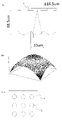
照射部1は、波長が940nmで、図6(a)に示すようなガウシアン配光である光を照射する単光源とした。また、光学素子2は、簡略的に、図6(b)に示すスリット状の開口がピッチ10μmで配列されたものとした。なお、光学素子のスリット以外の部分は光を完全に吸収する材料とした。また、照射部1と光学素子2の距離Lは、30μmから400μmまで10μmずつ変化させた38種類と、式Aのnが1~6の場合の53.19μm(n=1)、106.38μm(n=2)、159.67μm(n=3)、212.77μm(n=4)、265.96μm(n=5)、319.15μm(n=6)の6種類とした。図7~図9に光学シミュレーションソフトBeamPROP(Synopsys社製)を用いたシミュレーションの結果を示す。なお、横軸は配光角、縦軸は光源のパワーを1としたときの各配光角における遠方界の光強度である。[Simulation 1]
The
また、式Aのnが2,4,6の場合の106.38μm(n=2)、212.77μm(n=4)、319.15μm(n=6)の3種類について、それぞれ1μmずつ前後に10μm変化させたものについてもシミュレーションした。その結果を図10~15に示す。 In addition, about 1 μm each for the three types of 106.38 μm (n = 2), 212.77 μm (n = 4), and 319.15 μm (n = 6) when n in the formula A is 2, 4, and 6. A simulation was also performed for a change of 10 μm. The results are shown in FIGS. 10 to 15.
シミュレーションの結果、光強度分布は、距離Lが53.19μm(n=1)、106.38μm(n=2)、159.67μm(n=3)、212.77μm(n=4)、265.96μm(n=5)、319.15μm(n=6)である場合に、きれいなピークが出ていることがわかった。また、nが偶数である106.38μm(n=2)、212.77μm(n=4)、319.15μm(n=6)のときには、各ピークの光強度も大きいことがわかった。また、距離Lが式1を満たしていれば、比較的きれいなピークを維持しており、距離Lに多少の誤差があっても光強度は十分に強いことがわかる。
As a result of the simulation, the light intensity distribution was such that the distance L was 53.19 μm (n = 1), 106.38 μm (n = 2), 159.67 μm (n = 3), 212.77 μm (n = 4), 265. It was found that a clean peak appeared when the value was 96 μm (n = 5) and 319.15 μm (n = 6). It was also found that when n is an even number of 106.38 μm (n = 2), 212.77 μm (n = 4), and 319.15 μm (n = 6), the light intensity of each peak is also large. Further, it can be seen that if the distance L satisfies
[シミュレーション2]
照射部1は、波長が940nmで、図16(a)に示すようなガウシアン配光である光を照射する単光源とした。光学素子2は、図16(b)に示すように、高さが7μmのレンズ21をピッチが10μmで周期配列したものとした。また、レンズ表面は、非円弧状とした。材料は、屈折率が1.53のPDMSを想定した。距離Lは、式Aのnが1,2,4,6,8の場合の53.2μm(n=1)、106.4μm(n=2)、212.8μm(n=4)、319.1μm(n=6)、425.5μm(n=8)の5種類を用いた。図17に光学シミュレーションソフトBeamPROP(Synopsys社製)を用いたシミュレーションの結果を示す。なお、横軸は配光角、縦軸は光源のパワーを1としたときの各配光角における遠方界の光強度である。[Simulation 2]
The
シミュレーションの結果、光学素子2は、レンズ21を複数配列したものであっても、距離Lが53.2μm(n=1)、106.4μm(n=2)、212.8μm(n=4)、319.1μm(n=6)、425.5μm(n=8)である場合に、きれいなピークが出ており、各ピークの光強度も大きいことがわかる。また、nが偶数である106.4μm(n=2)、212.8μm(n=4)、319.1μm(n=6)、425.5μm(n=8)のときには、各ピークの光強度も大きいことがわかった。
As a result of the simulation, the
[シミュレーション3]
照射部1は、波長が940nmの光を照射する光源10を、図18(a)に示すように正方配列にした複数光源とした。また、光源が照射する光は、図18(b)に示すようなバットウィング配光で、遠方界において図18(c)に示すような光強度のものを用いた。光学素子2は、図19(a)に示すように、ピッチが20μmであるレンズ21を正方配列にしたものとした。また、各レンズ21の形状は、図19(b)に示すように、平面視が1辺20μmの正方形で、高さが9.86μmとした。また、レンズ表面は、x軸方向とy軸方向で曲率が異なる非回転対称の非球面とした。材料は、屈折率が1.53のPDMSを想定した。距離Lは、212.8μm(式Aのn=1の場合)、425.5μm(式Aのn=2の場合)、638.3μm(式Aのn=3の場合)とした。図20~図22に光学シミュレーションソフトBeamPROP(Synopsys社製)を用いたシミュレーションの結果を示す。なお、図20~図22の(a)は、光学素子2から50cm先のドットパターンを示す図である。ドットの大きさは光強度の大きさを表す。また、図20~図22の(b)は図20~図22の(a)のx軸上の光の遠方界の光強度を、図20~図22の(c)は図20~図22の(a)のy軸上の光の遠方界の光強度を示す。なお、横軸は配光角、縦軸は光源のパワーを1としたときの各配光角における遠方界の光強度である。[Simulation 3]
The
また、比較例として、上記ドットパターンと概ね同形状の照射パターンを形成できるディフューザを用いた場合のシミュレーションをした。図23に光学シミュレーションソフトLightTools(Synopsys社製)を用いたシミュレーションの結果を示す。図23(a)は、ディフューザから50cm先の照射パターンを示す図である。また、図23(b)は図23(a)のx軸上の光の遠方界の光強度を、図23(c)は図23(a)のy軸上の光の遠方界の光強度を示す。
Further, as a comparative example, a simulation was performed when a diffuser capable of forming an irradiation pattern having substantially the same shape as the above dot pattern was used. FIG. 23 shows the results of a simulation using the optical simulation software LightTools (manufactured by Synopsys). FIG. 23A is a diagram showing an
シミュレーションの結果、ドットパターンは、きれいにピークが出ており、各ピークの光強度も大きいことがわかる。また、ディフューザを用いたものと比較して、各ピークの光強度が非常に大きいことがわかる。また、光学素子2のレンズが正方配列の場合、対角線方向にも28.3μmのピッチが存在する。このピッチが式Aを満たすLは、425.5μmであるため、図20の結果よりも図21の結果の方が、各ピークがきれいに揃っており、光強度も大きいことがわかる。
As a result of the simulation, it can be seen that the dot pattern has clear peaks and the light intensity of each peak is also high. In addition, it can be seen that the light intensity of each peak is very high as compared with the one using the diffuser. Further, when the lenses of the
[シミュレーション4]
照射部1は、波長が940nmの光を照射する光源を、図24(a)に示すように六方配列にした複数光源とした。また、光源が照射する光は、図24(b)に示すようなバットウィング配光で、遠方界において図24(c)に示すような光強度のものを用いた。光学素子2は、図25(a)に示すように、ピッチが22.5μmであるレンズ21を六方配列にしたものとした。また、各レンズ21の形状は、図25(b)に示すように、平面視が正六角形で、高さが12.9μmとした。また、レンズ表面は、x軸方向とy軸方向で曲率が異なる非回転対称の非球面とした。材料は、屈折率が1.53のPDMSを想定した。距離Lは、269.3μm(式Aのn=1の場合)、538.6μm(式Aのn=2の場合)、807.8μm(式Aのn=3の場合)とした。図26~28に光学シミュレーションソフトBeamPROP(Synopsys社製)を用いたシミュレーションの結果を示す。なお、図26~28の(a)は、光学素子2から50cm先のドットパターンを示す図である。ドットの大きさは光強度の大きさを表す。また、図26~28の(b)は図26~28の(a)のx軸上の光の遠方界の光強度を、図26~28の(c)は図26~28の(a)のy軸上の光の遠方界の光強度を示す。なお、横軸は配光角、縦軸は光源のパワーを1としたときの各配光角における遠方界の光強度である。[Simulation 4]
The
また、比較例として、上記ドットパターンと概ね同形状の照射パターンを形成できるディフューザを用いた場合のシミュレーション結果を図29に示す。図29(a)は、ディフューザから50cm先の照射パターンを示す図である。また、図29(b)は図29(a)のx軸上の光の遠方界の光強度を、図29(c)は図29(a)のy軸上の光の遠方界の光強度を示す。
Further, as a comparative example, FIG. 29 shows a simulation result when a diffuser capable of forming an irradiation pattern having substantially the same shape as the above dot pattern is used. FIG. 29A is a diagram showing an
シミュレーションの結果、ドットパターンは、きれいにピークが出ており、各ピークの光強度も大きいことがわかる。また、ディフューザを用いたものと比較して、各ピークの光強度が非常に大きいことがわかる。 As a result of the simulation, it can be seen that the dot pattern has clear peaks and the light intensity of each peak is also high. In addition, it can be seen that the light intensity of each peak is very high as compared with the one using the diffuser.
[透過光の重複率]
また、光学素子2のレンズ形状について更に検討した。すると、レンズ21の表面の異なる位置を透過した光が同一方向に出射されると干渉が生じてしまい、ドットのコントラストを低下させる原因となることがわかった。したがって、光学素子は、レンズ21からの透過光の出射方向の重複率が低くなるように設計される方が好ましい。[Duplicate rate of transmitted light]
Further, the lens shape of the
[レンズ形状]
ここで、レンズからの透過光の出射方向はレンズ表面の傾きで決まる。すなわち、レンズからの透過光の出射方向の重複率は、レンズ表面の法線方向の重複率と同義である。したがって、レンズからの透過光の出射方向の重複率を低くするには、レンズ21を、表面の法線方向の重複率が低くなる形状にすればよい。例えば、レンズ21は、当該レンズ21の表面の断面における線にレンズ21が凹状から凸状又は凸状から凹状へ変化する変曲点や特異点があると、その前後にある凹部と凸部に法線方向の重複する面が生じる。[Lens shape]
Here, the emission direction of the transmitted light from the lens is determined by the inclination of the lens surface. That is, the overlap rate in the emission direction of the transmitted light from the lens is synonymous with the overlap rate in the normal direction of the lens surface. Therefore, in order to reduce the overlap rate in the emission direction of the transmitted light from the lens, the
[シミュレーション5]
図30に変曲点があるレンズの例を、図31に変曲点がないレンズの例を示す。図30(a)は、y=sinxの曲線をy軸を中心に回転させた形状であり、図中の丸で示す部分に変曲点があるレンズである。一方、図31(a)はy=2|sinx|の曲線をy軸を中心に回転させた形状であり、変曲点のないレンズである。また、図30(b)、図31(b)は、当該レンズを周期配列した光学素子を用いた場合のドットパターンの遠方界における光強度を示す。照射部1は、波長が940nmで、図16(a)に示すようなガウシアン配光である光を照射する単光源とした。光学素子2は、図16(b)に示すように、高さが10μmのレンズ21をピッチが10μmで周期配列したものとした。材料は、屈折率が1.53のPDMSを想定した。距離Lは、式Aのnが2の場合の106.4μm(n=2)を用いた。図31(b)、図32(b)に光学シミュレーションソフトBeamPROP(Synopsys社製)を用いたシミュレーションの結果を示す。なお、横軸は配光角、縦軸は光源のパワーを1としたときの各配光角における遠方界の光強度である。[Simulation 5]
FIG. 30 shows an example of a lens having an inflection point, and FIG. 31 shows an example of a lens having no inflection point. FIG. 30A is a lens in which the curve of y = sinx is rotated around the y-axis and has an inflection point in the portion indicated by the circle in the figure. On the other hand, FIG. 31A is a lens in which the curve of y = 2 | sinx | is rotated around the y-axis and has no inflection. Further, FIGS. 30 (b) and 31 (b) show the light intensity in the far field of the dot pattern when the optical element in which the lens is periodically arranged is used. The
図30(a)に示すレンズは、レンズの断面形状に変曲点を有するため、この部分でレンズの形状が凹状から凸状又は凸状から凹状に変化する。この場合、凸状部を透過した光と凹上部を透過した光が同じ方向に進む領域が生じるため、図30(b)に示すように、干渉によってドットの間にノイズ光が生じ、コントラストを下げる要因となる。一方、図31(a)に示すレンズは、レンズの断面形状に変曲点がないため、レンズの形状が凸状部のみで構成される。この場合、透過した光が重複することがないため、図31(b)に示すように、ノイズ光のないきれいなドットパターンを形成することができる。したがって、レンズ21の表面の断面における線に変曲点や特異点はない方が好ましく、また、このような点あったとしても、凹部又は凸部のいずれかが十分に大きい形状にする方がよい。
Since the lens shown in FIG. 30A has an inflection point in the cross-sectional shape of the lens, the shape of the lens changes from concave to convex or from convex to concave at this portion. In this case, there is a region where the light transmitted through the convex portion and the light transmitted through the concave portion travel in the same direction. Therefore, as shown in FIG. 30B, noise light is generated between the dots due to the interference, and the contrast is increased. It becomes a factor to lower. On the other hand, in the lens shown in FIG. 31A, since there is no inflection in the cross-sectional shape of the lens, the shape of the lens is composed of only a convex portion. In this case, since the transmitted light does not overlap, a clean dot pattern without noise light can be formed as shown in FIG. 31 (b). Therefore, it is preferable that the line in the cross section of the surface of the
なお、レンズ21の表面の法線方向の重複率は、次のようにして測定することができる。
(1)図32(a)に示すように、レンズ21を平面視(x-y平面)で正方形の微細領域210としてn個に分割する。そして、それぞれの微細領域210に重複しない1~nの番号を付与する。なお、微細領域210の1辺の大きさは、少なくとも照射部の光の波長の4分の1(λ/4)以下とする。
(2)図32(a)に示すように、分割した微細領域210のうちi番目(i=1,2,・・・,n)の微細領域の中心点をPi、内接する円をCiとする。また、分割した微細領域210のうちi番目以外の微細領域の中心点群をQiとする。
(3)図32(b)に示すように、点Piを通るx-y平面に垂直な線(z軸に平行な線)とレンズ表面の交点における法線ベクトルをNpi、円Ciを通るx-y平面に垂直な線(z軸に平行な線)とレンズ表面との交点における法線ベクトル群をNciとする。そして、図32(c)に示すように、NpiとNciのなす角の最小値をδθiとする。
(4)図32(b)に示すように、点群Qiを通るx-y平面に垂直な線(z軸に平行な線)とレンズ表面の交点における法線ベクトル群をNqiとする。
(5)分割した微細領域210のうちi番目の微細領域の状態フラグをFiとし、Fiの初期値を0とする。
(6)図32(d)に示すように、全てのi=1,2,・・・,nに対して、法線ベクトルNpiとベクトル群Nqiのなす角θiを計算し、θi<δθi以下の場合は、Fiを1に設定する。
(7)Fiが1である個数をmとすると、法線重複率は(m/n)×100(%)で求めることができる。なお、法線重複率は、nを無限大にする(n→∞)と収束する。The overlap rate in the normal direction of the surface of the
(1) As shown in FIG. 32 (a), the
(2) As shown in FIG. 32 (a), the center point of the i-th ( i = 1, 2, ..., N) fine region of the divided
(3) As shown in FIG. 32 (b), the normal vector at the intersection of the line perpendicular to the xy plane (the line parallel to the z-axis ) passing through the point Pi and the lens surface is N pi and the circle C i . Let N ci be the normal vector group at the intersection of the line perpendicular to the xy plane (the line parallel to the z-axis) passing through the lens surface. Then, as shown in FIG. 32 (c), the minimum value of the angle formed by N pi and N ci is δ θ i .
(4) As shown in FIG. 32 (b), let N qi be a normal vector group at the intersection of a line perpendicular to the xy plane (a line parallel to the z axis) passing through the point group Q i and the lens surface. ..
(5) The state flag of the i -th fine region of the divided
(6) As shown in FIG. 32 (d), the angle θ i formed by the normal vector N p i and the vector group N qi is calculated for all i = 1, 2, ..., N, and θ If i <δθ i or less, set Fi to 1.
(7) Assuming that the number of Fis being 1 is m, the normal overlap rate can be obtained by (m / n ) × 100 (%). The normal overlap rate converges when n is set to infinity (n → ∞).
[シミュレーション6]
次に、レンズ形状の法線重複率と遠方界における光強度分布の関係についてシミュレーションをした。シミュレーションには、6種類のレンズをモデルとした。なお、後述するレンズ形状の数式は、光軸方向をz軸とし、それに直行する方向をx軸、y軸として表す。なお、照射部1は、波長が940nmの光を照射する光源10を、図18(a)に示すように正方配列にした複数光源とした。また、光源が照射する光は、図18(b)に示すようなバットウィング配光で、遠方界において図18(c)に示すような光強度のものを用いた。光学素子2は、平面形状がx=20μm、y=20μmの正方形で、ピッチが20μmであるレンズ21を正方配列にしたものとした。材料は、屈折率が1.53のPDMSを想定した。距離Lは、425.5μm(式Aのn=2の場合)とした。シミュレーションには、光学シミュレーションソフトBeamPROP(Synopsys社製)を用いた。[Simulation 6]
Next, we simulated the relationship between the normal overlap rate of the lens shape and the light intensity distribution in the distant field. Six types of lenses were used as models for the simulation. In the lens shape formula described later, the optical axis direction is the z-axis, and the directions perpendicular to the optical axis direction are the x-axis and the y-axis. The
[モデル1]
モデル1として図33(a)に示すレンズについて説明する。レンズの形状は次の式の通りである。

The lens shown in FIG. 33 (a) will be described as a
[モデル2]
モデル2として図34(a)に示すレンズについて説明する。レンズの形状は次の式の通りである。

The lens shown in FIG. 34 (a) will be described as a
[モデル3]
モデル3として図35(a)に示すレンズについて説明する。レンズの形状は次の式の通りである。

The lens shown in FIG. 35 (a) will be described as a
[モデル4]
モデル4として図36(a)に示すレンズについて説明する。レンズの形状は次の式の通りである。

The lens shown in FIG. 36 (a) will be described as a
[モデル5]
モデル5として図37(a)に示すレンズについて説明する。レンズの形状は次の式の通りである。

The lens shown in FIG. 37 (a) will be described as a
[モデル6]
モデル6として図38(a)に示すレンズについて説明する。レンズの形状は次の式の通りである。

The lens shown in FIG. 38 (a) will be described as a
以上の結果より、レンズ21の表面は、法線方向の重複率が10%以下、好ましくは5%以下、更に好ましくは3%以下となる形状がよい。また、レンズ21の表面は、レンズ21からの透過光の遠方界における重複率が10%以下、好ましくは5%以下、更に好ましくは3%以下である方がよい。
From the above results, the surface of the
[アパーチャーマスク]
また、上述したような透過光の重複率の低いレンズ形状を設計することが難しい場合がある。また、透過光の重複率の低いレンズ形状を設計できたとしても、製造上、そのようなレンズ形状を再現することが難しい場合もある。このような場合、光学系装置は、開口70を有し、光の一部を遮蔽するアパーチャーマスク7を有していてもよい。具体的には、必要な透過光(以下、有効光という)を通す開口70を有し、ノイズとなる透過光(以下、ノイズ光という)を遮蔽するアパーチャーマスク7を用いればよい。ここで、有効光とは、ドットパターンの形成に寄与する光を意味する。したがって、開口70は、少なくともレンズの光軸を含む部分に形成される。また、開口70の大きさは、できる限り有効光を透過させることができる大きさに形成されるのが好ましい。また、ノイズ光とは、前記重複率を上げる光を意味する。レンズとアパーチャーマスク7との距離はノイズ光を遮蔽できれば任意でよいが、隣接するレンズの有効光の光路が重なる範囲よりレンズ側に配置されるのが望ましい。例えば、隣接するレンズ同士が接している場合には、それぞれのレンズの有効光は、レンズの焦点までの距離の2倍を超えると重なる。したがって、アパーチャーマスク7は、レンズの焦点までの距離の2倍の距離よりレンズ側に配置される方がよい。また、アパーチャーマスク7の開口70を焦点位置に配置すると、開口70を最も小さくでき、ノイズ光の多くを遮蔽できる点で好ましい。[Aperture mask]
In addition, it may be difficult to design a lens shape having a low overlap rate of transmitted light as described above. Further, even if a lens shape having a low overlap rate of transmitted light can be designed, it may be difficult to reproduce such a lens shape in manufacturing. In such a case, the optical system device may have an
また、例えばレンズ21同士の境界部分は特異点となり、光が散乱してノイズ光の原因となる。また、例えばインプリント法によってレンズ21を形成する場合、レンズ21同士の境界部分には歪みが生じやすく、透過光の重複率を上げる原因となりやすい。したがって、このようなレンズ21の境界部分に当該レンズ21の透過光を遮蔽するアパーチャーマスク7を形成してもよい。また、アパーチャーマスク7は、光源と光学素子の間に配置することもできる。例えば、レンズ21の境界部分に光源からの光を遮蔽するアパーチャーマスク7を形成すればよい。
Further, for example, the boundary portion between the
また、アパーチャーマスク7の開口70の形状は、有効光を通すことができればどのような形状でもよく、円状、楕円状、四角形状、六角形状等の任意の形状にすることができる。また、レンズごとに開口70が形成されたものでもよいし、レンズごとの開口70同士がつながっているものでもよい。
Further, the shape of the
また、アパーチャーマスク7の材料としては、光の透過を抑制できるものであればどのようなものでもよいが、例えば、照射部からの光を吸収する吸収材や、当該光を反射する反射材を用いることができる。光を吸収する吸収材としては、例えばブラックレジストを用いることができる。また、光を反射する反射材としては、例えば銀、アルミニウム、酸化クロム等の金属を用いることができる。
The material of the
なお、アパーチャーマスク7は、光学素子と別体として構成されてもよいし、光学素子と一体に形成されていてもよい。
The
[シミュレーション7]
アパーチャーマスク7の有無によるノイズ光の影響についてシミュレーションした。照射部1は、波長が940nmの光を照射する光源10を、図18(a)に示すように正方配列にした複数光源とした。また、光源が照射する光は、図18(b)に示すようなバットウィング配光で、遠方界において図18(c)に示すような光強度のものを用いた。光学素子2は、図39(a)に示すように、ピッチが33μmであるレンズ21を正方配列にしたものとした。また、各レンズ21の形状は、図39(b)に示すように、次の式

The effect of noise light due to the presence or absence of the
アパーチャーマスク7がない場合には、図40に示すように、中心付近のドット間に、ノイズ光である小さなドットが生じているのがわかる。一方、アパーチャーマスク7を配置した場合には、図41に示すように、中心付近のドット間に、ノイズ光によるドットが生じておらず、きれいなドットパターンを形成していることがわかる。
In the absence of the
[シミュレーション8]
次に、アパーチャーマスク7と遠方界における光強度分布の関係についてシミュレーションをした。シミュレーションには、4種類のレンズをモデルとした。また、レンズの平面形状はx=20μm、y=20μmの正方形と、ピッチも20μmとした。なお、シミュレーションには、光学シミュレーションソフトBeamPROP(Synopsys社製)を用いた。[Simulation 8]
Next, a simulation was performed on the relationship between the
[モデル1]
図42(a)にアパーチャーマスク7がない場合のモデル1を示す、レンズの周期は10μm、レンズ高さは5μmとし、インプリント法でレンズを作成した場合に特異点になりやすいレンズの境界部分の形状を0.5μm径の円弧状とした。この場合の光強度を図42(b)に示す。中心付近のピーク間に、ノイズ光である小さなピークが生じているのがわかる。[Model 1]
FIG. 42 (a) shows
[モデル2]
次に、レンズ21の境界部分の底部側に、レンズ21からの透過光を遮蔽するアパーチャーマスク7を形成したモデル2を図43(a)に示す。アパーチャーマスク7の幅は、0.5μm径の円弧の幅に合わせて1μmとした。また、遮蔽部の厚さは0.5μmとした。この場合の光強度を図43(b)に示す。アパーチャーマスク7がないモデル1に比べ、中心部のノイズ光がほとんど発生していないことが分かる。[Model 2]
Next, FIG. 43A shows a
[モデル3]
モデル1のレンズにおいて、境界部分の円弧状の部分は、インプリント法で作成した際に歪みが生じ易い。そこで、図44(a)に示すように、モデル1のレンズの円弧状の部分を幅1μmの平坦な形状とし、モデル3とした。モデル3では、レンズ21の境界部分の底部側に、レンズ21からの透過光を遮蔽するアパーチャーマスク7を形成した。アパーチャーマスク7の幅は、平坦な部分の幅に合わせて1μmとした。また、遮蔽部の厚さは0.5μmとした。この場合の光強度を図44(b)に示す。アパーチャーマスク7がないモデルに比べ、中心部のノイズ光がほとんど発生していないことが分かる[Model 3]
In the lens of the
[モデル4]
次に、レンズ21の境界部分の表面に、光源からの光を遮蔽するアパーチャーマスク7を形成したモデル4を図45(a)に示す。アパーチャーマスク7の幅は、0.5μm径の円弧に入射する光を全て遮蔽することができるように1μmとした。この場合の光強度を図45(b)に示す。アパーチャーマスク7がないモデル1に比べ、中心部のノイズ光がほとんど発生していないことが分かる。[Model 4]
Next, FIG. 45A shows a
[光拡散部]
また、光学素子は、レンズの境界部分に透過光を当該レンズの照射角の外側(ドットパターンの照射範囲の外側)に屈折させる光拡散部8が形成されていてもよい。これにより、ノイズ光をドットパターンの外側に追い出すことができるので、きれいなドットパターンを得ることができる。光拡散部8の形状は入射した光をレンズの照射角の外側に屈折させることができればどのような形状でもよく、製造し易い任意の形状を選択すればよい。例えば、レンズの境界に平行な面による断面形状が三角形であるものを採用することができる。[Light diffuser]
Further, the optical element may have a
[シミュレーション9]
光拡散部8の有無によるノイズ光の影響についてシミュレーションした。図46(a)に示すように、レンズはシミュレーション7に用いたレンズの境界部分に光拡散部8を有する形状とした。光拡散部8は、レンズの周囲を境界から1.5μmの幅で形成した。光拡散部8の断面形状(レンズの直近の境界に対して平行な断面)は、図46(b)に示すように、底辺の幅と高さが同じであるアスペクト1の相似形の三角形を並べた凹凸構造とした。相似形の各三角形は、当該三角形の底辺の位置とレンズの底面の位置が一致するように並べた。その他は、シミュレーション7と同じ条件とした。光拡散部8がある場合のドットパターンを図47に示す。[Simulation 9]
The effect of noise light due to the presence or absence of the
光拡散部8を配置した場合には、図47に示すように、ドット間にノイズ光によるドットがあまり生じておらず、きれいなドットパターンを形成していることがわかる。
When the
[光学素子製造方法]
光学素子の製造方法について説明する。光学素子2のレンズ21は、どのように製造してもよいが、例えば、インプリント法を用いて製造することができる。具体的には、スピンコータ等の周知の方法によって、基板25上にレンズ21の材料を所定の膜厚で塗布する(塗布工程)。材料としては、波長λの光を透過するレンズ21を形成できればどのようなものでもよく、例えばポリジメチルシロキサン(PDMS)を用いることができる。[Optical element manufacturing method]
A method of manufacturing an optical element will be described. The
次に、レンズ21が周期的に配列されたパターンの反転パターンを有するモールドを用意し、当該モールドを基板25上に塗布した材料に加圧して、パターンを転写する(インプリント工程)。なお、上述した光拡散部8を有する光学素子を形成する場合には、前記パターンと共に当該光拡散部8の反転パターンを有するモールドを用いればよい。
Next, a mold having a pattern inversion pattern in which the
これにより、レンズ21の高さ方向のばらつきが小さい光学素子を製造することができるため、距離L1の誤差を小さくすることができる。As a result, it is possible to manufacture an optical element having a small variation in the height direction of the
また、光学素子にアパーチャーマスク7を形成する場合には、アパーチャーマスク形成工程を有する。まず、アパーチャーマスク7がレンズ21のノイズ光の光路に配置されるよう形成する場合について説明する。
Further, when the
(1)図48(a)に示すように、基板25上であって、少なくともレンズ21の光軸にあたる位置から所定距離離れた位置に光が透過するのを防止するアパーチャーマスク7を形成する(アパーチャーマスク形成工程)。アパーチャーマスク7はどのような方法で形成してもよいが、例えば、以下の方法で形成すればよい。
(1.1)基板25上に遮光材料からなる膜を形成する。当該膜の形成は化学蒸着(CVD)等の方法を用いてもよいし、塗布によって形成してもよい。
(1.2)遮光材料からなる膜の上にレジストを塗布し、フォトリソグラフィやインプリント等の既存の技術によって、アパーチャーマスクの開口となる部分以外の位置にレジストを形成する。開口70の大きさは、できる限り有効光を透過させることができる大きさに形成すればよい。このレジストを用いて遮光材料をエッチングし、残ったレジストをアッシング等により除去すれば、アパーチャーマスク7を形成することができる。(1) As shown in FIG. 48 (a), an
(1.1) A film made of a light-shielding material is formed on the
(1.2) A resist is applied on a film made of a light-shielding material, and a resist is formed at a position other than the opening portion of the aperture mask by existing techniques such as photolithography and imprint. The size of the
遮光材料としては使用する光を遮光できればどのような材料を用いてもよいが、例えば、銀、アルミニウム、酸化クロム等の金属やブラックレジスト等の樹脂を用いることができる。 As the light-shielding material, any material may be used as long as it can block the light to be used, and for example, a metal such as silver, aluminum or chromium oxide or a resin such as black resist can be used.
(2)基板25上にアパーチャーマスク7を形成した後、図48(b)に示すように、レンズ21とアパーチャーマスク7との距離を調節するための透明膜26を形成する。透明膜26はどのように形成してもよく、例えば、スピンコータ等の周知の方法によって、基板25上に透明な材料を所定の膜厚で塗布して形成すればよい。材料としては、波長λの光を透過するものであればどのようなものでもよく、例えばポリジメチルシロキサン(PDMS)を用いることができる。
(2) After forming the
(3)基板25上に透明膜26を形成した後、図48(c)に示すように、レンズ21を形成する(レンズ形成工程)。レンズはどのような方法で形成してもよいが、例えば、アパーチャーマスク7との位置合わせを行い、インプリント法等の既存の技術を用いてレンズ21を形成すればよい。この場合、レンズ21とアパーチャーマスク7との距離は、透明膜26とインプリントによる残膜の大きさによって決まる。このようにして、図48(d)に示すように、光学素子2と一体となったアパーチャーマスク7を形成することができる。なお、レンズ21とアパーチャーマスク7との距離の調節は、透明膜26を形成せずに、インプリントによる残膜の大きさのみによって調節することも可能である。
(3) After forming the
また、図49(c)に示すように、レンズ21の境界部分であってレンズの透過光側に、レンズからの透過光を遮蔽するアパーチャーマスク7を形成する場合には、以下の方法で形成すればよい。
Further, as shown in FIG. 49 (c), when the
(1)図49(a)に示すように、基板25上であって、レンズの境界にあたる位置に光が透過するのを防止するアパーチャーマスク7を形成する(アパーチャーマスク形成工程)。アパーチャーマスク7は従来から知られているどのような方法で形成してもよいが、例えば、以下の方法で形成すればよい。
(1.1)基板25上に遮光材料からなる膜を形成する。当該膜の形成は化学蒸着(CVD)等の方法を用いてもよいし、塗布によって形成してもよい。
(1.2)遮光材料からなる膜の上にレジストを塗布し、フォトリソグラフィやインプリント等の既存の技術によって、レンズの境界にあたる位置にのみ、ノイズ光を遮蔽できる所望の幅でレジストを形成する。このレジストを用いて遮光材料をエッチングし、残ったレジストをアッシング等により除去すれば、アパーチャーマスク7を形成することができる。(1) As shown in FIG. 49 (a), an
(1.1) A film made of a light-shielding material is formed on the
(1.2) A resist is applied on a film made of a light-shielding material, and a resist is formed with a desired width that can block noise light only at the position corresponding to the boundary of the lens by existing techniques such as photolithography and imprint. do. The
遮光材料としては使用する光を遮光できればどのような材料を用いてもよいが、例えば、銀、アルミニウム、酸化クロム等の金属やブラックレジスト等の樹脂を用いることができる。 As the light-shielding material, any material may be used as long as it can block the light to be used, and for example, a metal such as silver, aluminum or chromium oxide or a resin such as black resist can be used.
(2)基板25上にアパーチャーマスク7を形成した後、図49(b)に示すように、アパーチャーマスク7上にレンズ21の境界が配置されるようにレンズ21を形成する(レンズ形成工程)。レンズはどのような方法で形成してもよいが、例えば、アパーチャーマスク7との位置合わせを行い、インプリント法等の既存の技術を用いてレンズ21を形成すればよい。これにより、図49(c)に示すように、光学素子2と一体となったアパーチャーマスク7を形成することができる。
(2) After forming the
また、図50(c)に示すように、レンズ21の境界部分であってレンズの光源側に、光源からの光を遮蔽するアパーチャーマスク7を形成する場合には、以下の方法で形成すればよい。
Further, as shown in FIG. 50 (c), when the
(1)レンズ21が周期的に配列された光学素子を用意する。当該光学素子のレンズ21の形成はどのように行ってもよく、例えばインプリント法などの既存の技術を用いればよい。
(2)次に、図50(a)に示すように、レンズ21上の全部または一部に光が透過するのを防止する遮光材料を塗布し遮光膜27を形成する。次に、図50(b)に示すように、当該レンズ21の境界にあたる位置に遮光材料の一部が残るように遮光材料を除去してアパーチャーマスク7を形成する(アパーチャーマスク形成工程)。例えば、レンズ21上にブラックレジスト等の遮光材料を塗布する。この遮光材料をエッチングにより所望量だけエッチバックしてやればレンズ21の境界にあたる溝の部分にのみ遮光材料が残った状態の光学素子を形成することができる。(1) Prepare an optical element in which the
(2) Next, as shown in FIG. 50 (a), a light-shielding material for preventing light from being transmitted is applied to all or part of the
遮光材料としては、使用する光を遮光することができ、レンズ21に対するエッチングレートが十分に高ければどのような材料を用いてもよい。ここでエッチングレートが十分に高いとは、レンズ21の光学特性に影響がない程度を意味する。
エッチング方法はエッチバックができればどのような方法を用いてもよいが、例えば反応性イオンエッチング(RIE)やケミカルドライエッチング(CDE)などを用いればよい。これにより、図50(c)に示すように、光学素子2と一体となったアパーチャーマスク7を形成することができる。As the light-shielding material, any material may be used as long as it can block the light to be used and the etching rate with respect to the
Any etching method may be used as long as etch back is possible, and for example, reactive ion etching (RIE) or chemical dry etching (CDE) may be used. As a result, as shown in FIG. 50 (c), the
[照射部のピッチ]
照射部1に複数の光源10を有する場合には、各光源10と光学素子2を相対的に平行移動しても、平面視で、光学素子2の各レンズ21に対する光源10の数が同じになるように配置する必要がある。具体的には、mを1以上の自然数とすると、照射部は、光学素子のレンズ21のいずれかの周期方向に対して、複数の光源を当該周期のm倍又は1/m倍で規則的に配列するとよい。換言すると、照射部1の光源10は、光学素子2のレンズ21がピッチPkをとる方向に対して、ピッチmPk又はPk/mで規則的に配列するとよい。特に、ピッチmP1又はP1/mとするのがよい。図51の(a),(b)は、m=1として、光源10のピッチを光学素子2のレンズ21のピッチP1と等しくしたものである。また、図51(c)は、m=2とし、光源10のピッチを光学素子2のレンズ21のピッチP1の1/2、すなわちP1/2としたものである。また、図51(d)は、m=2とし、光源10のピッチを光学素子2のレンズ21のピッチP1の2倍、すなわち2P1としたものである。[Pitch of irradiation part]
When the
なお、照射部1が光源10を六方配列としたものである場合には、光学素子のレンズ21の平面形状を長方形とし、当該長方形の短辺と長辺の比をP1:P2=1:√3とし、光源10のピッチをmP1又はP1/mすると、各レンズ21に対する光源10の数が均一になるため好ましい。また、この場合には、最も小さいピッチP1(長方形の短辺の大きさ)と2番目に小さいピッチP2(長方形の長辺の大きさ)について式1を満たすために、P2=√3P1を考慮して、照射部1と光学素子2との距離L1は、


また、照射部1の光は、図52に示すように、直接光学素子2に照射する必要はなく、照射部1の光を反射するミラー3を介して照射してもよい。この場合、照射部1と光学素子2との距離L1とは実質的な距離を意味する。したがって、図52の場合の距離L1は、矢印で示す照射部1からミラー3までの距離Laとミラー3から光学素子2までの距離Lbの和であるLa+Lbとなる。これにより、ミラー3を用いて距離Lを調節することができる。また、光源からの光の方向を調節することも可能である。Further, as shown in FIG. 52, the light of the
次に、本発明の別の実施形態について説明する。図53(a)は、光学素子2側から照射部1を見た概略平面図である。ここで、光学素子2は、平面形状が長方形のレンズ21を規則的に配列にしたものとした。また、照射部1は、各光源10を六方配列にしたものを用いた。図53(a)に示す光源10の配置は、分解すると図53(b)に示すように4つに分けることができる。このうち、図53(b)の左上と左下および右上と右下の光源10の配置から照射されるドットパターンは同一であるため、同一視することができる。したがって、光学素子2に対する光源10の配置としては、実質的には図53(c)に示す2種類に分類することができる。
Next, another embodiment of the present invention will be described. FIG. 53A is a schematic plan view of the
したがって、図54に示すように、照射部1を、波長λの光を照射する複数の光源10を規則的に配列した第1照射部1Aと、波長λの光を照射する複数の光源10を前記第1照射部1Aの光源10と縦および横に半周期ずつずらして規則的に配列した第2照射部1Bと、で構成しても同様の配光を実現することができる。この場合、図53の(a)と(c)を比較すればわかる通り、照射部1の光源10同士のピッチを2倍にすることができるという利点がある。
Therefore, as shown in FIG. 54, the
また、照射部1を、波長λの光を照射する複数の光源10を規則的に配列した第1照射部、第2照射部および第3照射部で構成し、各照射部を、光学素子2のレンズ21がピッチPkをとる方向に対してPk/3ずつずらして配列するようにしてもよい。例えば、光学素子2は、平面形状が長方形のレンズ21を規則的に配列にしたものとし、照射部1は、各光源10を六方配列にしたものを用いた場合を図55(a)に示す。この場合、図55(a)に示す照射部1は、図55(b)~(d)に示すように、光学素子2のレンズがピッチP2をとる方向に対して、光源10がP2/3ずつずらして配列された第1の照射部11、第2の照射部12、第3の照射部13の3つで構成することができる。したがって、図56に示すように、光学素子2と第1照射部11、第2照射部12および第3照射部13の3つで光学系装置を構成することにより、照射部の光強度を下げずに出射されるドットの数を3倍に増やすことができる。また、TOFに用いる受光センサの解像度が低い場合には、ドットの数が3倍になっても全てを感知することができない場合もある。この場合には、照射部は、第1照射部、第2照射部および第3照射部を時間をずらして順番に発光させるようにすることも可能である。これにより、受光センサで3回の測定を行うことにより、解像度を3倍に増やすことができる。Further, the
また、レンズ21の平面形状が、いずれかの辺の長さがRである正方形又は長方形の場合、当該レンズ21の配列は、iを1以上の自然数とすると、上述した辺の方向に連なるレンズ21の列同士を、R/iずつずらして配列してもよい。これにより、出射するドットの数をi倍にすることができる。
Further, when the planar shape of the
当該原理は、次のように説明することができる。なお、ここで照射部1は、波長が940nmの光を照射する光源10を最小ピッチが21μmとなるように六方配列にしたものとした。また、光源10の大きさは10μmであるとした。また、光学素子2のレンズ21の平面形状は、縦21μm、横36.4μmの長方形であるとした。また、照射部1と光学素子2の距離は1407μmとした。図57(a)に示すように、光学素子2の隣接する列のレンズ21が同一に配置される場合には、各レンズ21に対する光源10の位置を合成すると図57(b)に示すようになり、レンズ21の1個当たりの光源10の光は2個となる。この場合、照射されるドットパターンは、図57(c)のようになる。一方、図58(a)に示すように、光学素子2の隣接する列のレンズ21をR/2ずつずらして配列した場合には、各レンズ21に対する光源10の位置を合成すると図58(b)に示すようになり、レンズ21の1個当たりの光源10の光は4個となる。この場合、レンズ21の1個当たりの光源10の光が2倍になるため、照射されるドットパターンのドットの数は、図58(c)のように2倍になる。更に、図59(a)に示すように、光学素子2の隣接する列のレンズ21をR/3ずつずらして配列した場合には、各レンズ21に対する光源10の位置を合成すると図59(b)に示すようになり、レンズ21の1個当たりの光源10の光は6個となる。この場合、レンズ21の1個当たりの光源10の光が3倍になるため、照射されるドットパターンのドットの数は、図59(c)のように3倍になる。このように、光学素子2の隣接する列のレンズ21をR/iずつずらして配列した場合には、各レンズ21に対する光源10を合成すると、レンズ21の1個当たりの光源10の光は2i個となる。したがって、レンズ21の1個当たりの光源10の光は隣接するレンズ21の列を全くずらさない場合のi倍となり、出射されるドットの数もi倍となる。
The principle can be explained as follows. Here, the
また、本発明の光学素子2と、従来のディフューザ型の光学素子5を併用したい場合もある。この場合、光学系装置は、図60に示すように、照射部1の光を所定形状に拡散するディフューザと、光源10とディフューザとの間に配置され、照射部1の光の一部を透過し、一部を反射するハーフミラーと、ハーフミラー4が反射した光を光学素子2に反射するミラーと、を備えるようにしてもよい。
Further, there may be a case where the
また、本発明に係る光学素子2は、ドットパターンを照射するために用いることができるだけでなく、ディフューザ用途にも用いることもできる。
Further, the
光学素子2をディフューザとして用いる第1の方法は、図61に示すように、波長λの光を照射する複数の光源10をドットパターンの照射に利用する照射部1と同一に配列したディフューザ用照射部6を用意する。そして、ディフューザ用照射部6と光学素子2との距離L2が、下記式2

なお、より好ましくは、距離L2が、下記式3

なお、この場合、図61(a)に示すように、光学素子2を共通にして用いてもよいし、図61(b)に示すように、ドットパターン用の光学素子2aとディフューザ用の光学素子2bの2つを用いてもよい。
In this case, as shown in FIG. 61 (a), the
また、光学素子2をディフューザとして用いる第2の方法は、波長λの光を照射する複数の光源60を配列したディフューザ用照射部6を用意する。そして、mを1以上の自然数とすると、ディフューザ用照射部6は、光学素子2のレンズ21の周期方向に対して、複数の光源60を当該周期のm倍又は1/m倍とならないように配列すればよい。
Further, in the second method using the
なお、図62(a)に示すように、ディフューザ用照射部6の複数の光源60が当該周期のm倍又は1/m倍である場合もある。この場合には、図62(b)に示すように、光学素子に対するディフューザ用照射部6を光源60の光軸方向に対して回転させればよい。これにより、光学素子2のレンズ21の周期方向に対して、複数の光源60が当該周期のm倍又は1/m倍とならないように配列をずらすことができる。図63~図65は、光学素子2にディフューザ用照射部6の光を照射した場合の各レンズ21に対する光源60の位置を一つのレンズ21に合成した状態を示す図である。ここで回転角度θは、光学素子2のレンズ21がピッチPkをとる方向に対する、ディフューザ用照射部6の光源10がピッチmPk又はPk/mをとる方向の角度差を意味とする。例えば、図62(a)に示すように、照射部1のピッチと光学素子2のピッチが一致する場合(θが0度の場合)には、どのレンズ21においても光源10の位置が同一であるため、図63(θ=0°)に示すように、それぞれの光源10の位置がきれいに重なる。一方、角度θが大きくなるにつれて光源10の位置にずれが生じ始める。As shown in FIG. 62 (a), the plurality of
[シミュレーション10]
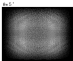
光学素子2に対する回転角度とドットパターンの関係についてシミュレーションをした。照射部は、ピッチは21μmの六方配列で、波長940nm、広がり角(FWHM)が20度、エミッターピッチが10μmのVCSELとした。光学素子は、屈折率が1.53、ピッチが21μm×36.37μmの長方形、FOIが60度×45度とした。また、光学素子と照射部の距離は1407μmとした。また、ドットパターンの投影位置は、光学素子から50cm先とした。光学素子2に対する回転角度θは、0度、1度、5度、10度、15度とした。図66~図70は、光学素子2に対する回転角度とドットパターンを示す図である。なお、シミュレーションには、光学シミュレーションソフトBeamPROP(Synopsys社製)を用いた。[Simulation 10]
A simulation was performed on the relationship between the rotation angle and the dot pattern with respect to the
図66に示すように、ディフューザ用照射部6の複数の光源60が光学素子のレンズの周期が一致している(回転角度が0度)場合には、きれいにドットパターンが出ているのに対し、回転角度が大きくなり、光源60の周期とレンズの周期のずれが大きくなるにつれて、ピーク幅が広がり、光が拡散しているのがわかる。したがって、光学素子に対するディフューザ用照射部6の回転角度θを適宜調節することにより、光学素子2をディフューザとして用いることができる。
As shown in FIG. 66, when the plurality of
また、光学素子2をディフューザとして用いる第3の方法は、ドットパターンのドットの数を増やして、照射される光を見かけ上均一にする方法である。ここで見かけ上とは、例えば、TOFに用いる場合には、照射された光の反射光を受光する受光センサの解像度以上にドットの数を大きくすることを意味する。ドットパターンのドットの数を増やすには、上述したように、レンズ21の平面形状を、いずれかの辺の長さがRである正方形、長方形、ひし型又は平行四辺形とする。また、当該レンズ21の配列は、上述した辺の方向に連なるレンズ21の列同士を、R/iずつずらして配列する。そして、出射するドットの数を受光センサの解像度以上となるようにiを調節すればよい。
Further, the third method of using the
このように形成されたディフューザは、上述したドットパターンを照射するための光学系装置と組み合わせて用いることができる。これにより、遠距離の対象物は、ドットパターンによって照射光のインテンシティを担保して距離や形状等を測定し、近距離の対象物はディフューザの光を照射して距離や形状等をより正確に測定することができる。 The diffuser formed in this way can be used in combination with an optical system device for irradiating the above-mentioned dot pattern. As a result, for long-distance objects, the intensity of the irradiation light is secured by the dot pattern and the distance and shape are measured, and for short-distance objects, the distance and shape are more accurate by irradiating the diffuser light. Can be measured.
1 照射部
1A 第1の照射部
1B 第2の照射部
2 光学素子
3 ミラー
4 ハーフミラー
5 ディフューザ型の光学素子
6 ディフューザ用照射部
7 アパーチャーマスク
8 光拡散部
10 光源
11 照射部
12 照射部
13 照射部
21 レンズ
25 基板
60 光源
70 開口1 Irradiation unit 1A 1st irradiation unit 1B
10 light source
11 Irradiation part
12 Irradiation part
13 Irradiated part
21 lens
25 board
60 light source
70 openings
Claims (18)
波長λの光を前記レンズの複数に照射する光源を有する照射部と、
を具備し、
nを1以上の自然数とし、前記レンズのピッチのうち小さいものからk番目(kは1以上の自然数)のピッチの大きさをPkとすると、いずれか1以上のピッチPkについて、前記照射部と前記光学素子の距離L1が、下記式1

を満たし、
前記レンズは、当該レンズ同士の境界が平面視で正方形、長方形又は六角形であって、表面の法線方向の重複率が10%以下である非球面レンズであることを特徴とする光学系装置。 An optical element in which lenses that transmit light of wavelength λ are periodically arranged, and
An irradiation unit having a light source that irradiates a plurality of the lenses with light having a wavelength λ, and an irradiation unit.
Equipped with
Assuming that n is a natural number of 1 or more and the size of the kth (k is a natural number of 1 or more) pitch from the smallest pitch of the lens is P k , the irradiation is performed on any one or more pitch P k . The distance L 1 between the unit and the optical element is the following equation 1.
The filling,
The lens is an aspherical lens in which the boundary between the lenses is a square, a rectangle, or a hexagon in a plan view, and the overlap ratio in the normal direction of the surface is 10% or less. ..
前記光学素子のレンズの平面形状は、短辺と長辺の比をP1:P2=1:√3とする長方形としたものであることを特徴とする請求項9記載の光学系装置。 Assuming that m is a natural number of 1 or more, the irradiation unit has the light sources arranged in a hexagonal arrangement with a pitch mP 1 or P 1 / m.
The optical system device according to claim 9, wherein the planar shape of the lens of the optical element is a rectangle having a ratio of a short side to a long side of P 1 : P 2 = 1: √3.
前記レンズの配列は、iを2以上の自然数とすると、前記辺の方向に連なるレンズの列同士が、R/iずつずらして配列されたものであることを特徴とする請求項1ないし16のいずれかに記載の光学系装置。 The planar shape of the lens is a square or a rectangle whose side length is R.
The arrangement of the lenses is characterized in that, assuming that i is a natural number of 2 or more, the rows of lenses connected in the direction of the sides are arranged so as to be shifted by R / i. The optical system device according to any one.
The irradiation unit is composed of a VCSEL having a plurality of light emitting modes, and the light emitting mode is characterized in that the ratio of the mode having the maximum intensity at the center of the optical axis is 40% or more of the whole, according to any one of claims 1 to 17. The optical system device described in Crab.
Applications Claiming Priority (5)
| Application Number | Priority Date | Filing Date | Title |
|---|---|---|---|
| JP2020084820 | 2020-05-13 | ||
| JP2020084820 | 2020-05-13 | ||
| JP2020135464 | 2020-08-08 | ||
| JP2020135464 | 2020-08-08 | ||
| PCT/JP2020/047275 WO2021229848A1 (en) | 2020-05-13 | 2020-12-17 | Optical device and optical element manufacturing method |
Publications (2)
| Publication Number | Publication Date |
|---|---|
| JPWO2021229848A1 JPWO2021229848A1 (en) | 2021-11-18 |
| JP7061823B2 true JP7061823B2 (en) | 2022-05-02 |
Family
ID=78524437
Family Applications (1)
| Application Number | Title | Priority Date | Filing Date |
|---|---|---|---|
| JP2021521863A Active JP7061823B2 (en) | 2020-05-13 | 2020-12-17 | Optical system equipment and optical element manufacturing method |
Country Status (4)
| Country | Link |
|---|---|
| US (1) | US20230204824A1 (en) |
| JP (1) | JP7061823B2 (en) |
| CN (1) | CN115552278A (en) |
| WO (2) | WO2021229848A1 (en) |
Cited By (1)
| Publication number | Priority date | Publication date | Assignee | Title |
|---|---|---|---|---|
| JPWO2023026987A1 (en) * | 2021-08-25 | 2023-03-02 |
Families Citing this family (3)
| Publication number | Priority date | Publication date | Assignee | Title |
|---|---|---|---|---|
| WO2023090435A1 (en) * | 2021-11-19 | 2023-05-25 | Scivax株式会社 | Optical system device and method for manufacturing optical element |
| CN217034418U (en) * | 2022-01-11 | 2022-07-22 | 深圳迈塔兰斯科技有限公司 | Optical system and photocuring printing system comprising same |
| WO2024029616A1 (en) * | 2022-08-05 | 2024-02-08 | Scivax株式会社 | Optical element, optical system device, and optical system device manufacturing method |
Citations (5)
| Publication number | Priority date | Publication date | Assignee | Title |
|---|---|---|---|---|
| JP2000298201A (en) | 1999-04-14 | 2000-10-24 | Omron Corp | Microlens array |
| JP2002277610A (en) | 2001-03-21 | 2002-09-25 | Ricoh Co Ltd | Method for manufacturing microlens substrate with light shielding part |
| JP2005156203A (en) | 2003-11-21 | 2005-06-16 | Matsushita Electric Works Ltd | Laser range finder |
| WO2017131585A1 (en) | 2016-01-26 | 2017-08-03 | Heptagon Micro Optics Pte. Ltd. | Multi-mode illumination module and related method |
| JP2018511034A (en) | 2015-01-29 | 2018-04-19 | ヘプタゴン・マイクロ・オプティクス・プライベート・リミテッドHeptagon Micro Optics Pte. Ltd. | Apparatus for generating patterned illumination |
Family Cites Families (3)
| Publication number | Priority date | Publication date | Assignee | Title |
|---|---|---|---|---|
| JPH0264501A (en) * | 1988-08-30 | 1990-03-05 | Sharp Corp | Microlens array and production thereof |
| US11624832B2 (en) * | 2018-06-08 | 2023-04-11 | Samsung Electronics Co., Ltd. | Illumination device and electronic device including the same |
| US11175010B2 (en) * | 2018-09-20 | 2021-11-16 | Samsung Electronics Co., Ltd. | Illumination device and electronic apparatus including the same |
-
2020
- 2020-12-17 JP JP2021521863A patent/JP7061823B2/en active Active
- 2020-12-17 CN CN202080100825.4A patent/CN115552278A/en active Pending
- 2020-12-17 WO PCT/JP2020/047275 patent/WO2021229848A1/en active Application Filing
- 2020-12-17 US US17/924,936 patent/US20230204824A1/en active Pending
-
2021
- 2021-05-13 WO PCT/JP2021/018246 patent/WO2021230324A1/en active Application Filing
Patent Citations (5)
| Publication number | Priority date | Publication date | Assignee | Title |
|---|---|---|---|---|
| JP2000298201A (en) | 1999-04-14 | 2000-10-24 | Omron Corp | Microlens array |
| JP2002277610A (en) | 2001-03-21 | 2002-09-25 | Ricoh Co Ltd | Method for manufacturing microlens substrate with light shielding part |
| JP2005156203A (en) | 2003-11-21 | 2005-06-16 | Matsushita Electric Works Ltd | Laser range finder |
| JP2018511034A (en) | 2015-01-29 | 2018-04-19 | ヘプタゴン・マイクロ・オプティクス・プライベート・リミテッドHeptagon Micro Optics Pte. Ltd. | Apparatus for generating patterned illumination |
| WO2017131585A1 (en) | 2016-01-26 | 2017-08-03 | Heptagon Micro Optics Pte. Ltd. | Multi-mode illumination module and related method |
Cited By (2)
| Publication number | Priority date | Publication date | Assignee | Title |
|---|---|---|---|---|
| JPWO2023026987A1 (en) * | 2021-08-25 | 2023-03-02 | ||
| JP7418050B2 (en) | 2021-08-25 | 2024-01-19 | Scivax株式会社 | optical system equipment |
Also Published As
| Publication number | Publication date |
|---|---|
| US20230204824A1 (en) | 2023-06-29 |
| WO2021229848A1 (en) | 2021-11-18 |
| CN115552278A (en) | 2022-12-30 |
| JPWO2021229848A1 (en) | 2021-11-18 |
| WO2021230324A1 (en) | 2021-11-18 |
Similar Documents
| Publication | Publication Date | Title |
|---|---|---|
| JP7061823B2 (en) | Optical system equipment and optical element manufacturing method | |
| US9052512B2 (en) | Diffractive optical element and measuring apparatus | |
| US8469549B2 (en) | Beam shaper | |
| CN108351437B (en) | Diffusion plate, method for designing diffusion plate, method for manufacturing diffusion plate, display device, projection device, and illumination device | |
| JP2013210680A (en) | Diffraction optical element, method of manufacturing the same, and laser machining method | |
| JP6186679B2 (en) | Illumination optical system, measuring apparatus, and diffractive optical element used therefor | |
| JP6070274B2 (en) | Diffusion element, illumination optical system and measuring device | |
| KR102439748B1 (en) | Optical element and optical system | |
| JP2011107195A (en) | Optical element, method of manufacturing the same, minutely rugged structure, and molding die | |
| JP7436369B2 (en) | Microstructure that converts light with Lambertian distribution into batwing distribution | |
| JP2019139163A (en) | Diffusion plate, method for designing diffusion plate, display device, projection device, and illumination device | |
| US11536981B2 (en) | Diffractive optical element, projection device, and measurement device | |
| CN114556168A (en) | Diffusion plate, display device, projection device, and illumination device | |
| JP2023105236A (en) | Optical eyepiece using single-sided patterning of grating couplers | |
| JP6755076B2 (en) | Optical elements, projection devices and measuring devices | |
| US5223978A (en) | Hybrid diffractive/refractive lens | |
| CN216792482U (en) | Light uniformizing element | |
| JP7301513B2 (en) | speckle reduction module | |
| KR20210118868A (en) | diffuser plate | |
| US9353929B2 (en) | Beam diffusing module and beam generating system | |
| JP7238252B2 (en) | Diffractive optical element, light irradiation device | |
| TW202332937A (en) | Optical system device and method for manufacturing optical element | |
| WO2023097850A1 (en) | Diffractive optical element and preparation method therefor, and method for designing master diffraction pattern | |
| JP2020106771A (en) | Diffraction optical element and optical system device using the same | |
| WO2023026987A1 (en) | Optical system device |
Legal Events
| Date | Code | Title | Description |
|---|---|---|---|
| A521 | Request for written amendment filed |
Free format text: JAPANESE INTERMEDIATE CODE: A523 Effective date: 20210518 |
|
| A621 | Written request for application examination |
Free format text: JAPANESE INTERMEDIATE CODE: A621 Effective date: 20210518 |
|
| A871 | Explanation of circumstances concerning accelerated examination |
Free format text: JAPANESE INTERMEDIATE CODE: A871 Effective date: 20210518 |
|
| A131 | Notification of reasons for refusal |
Free format text: JAPANESE INTERMEDIATE CODE: A131 Effective date: 20210907 |
|
| A521 | Request for written amendment filed |
Free format text: JAPANESE INTERMEDIATE CODE: A523 Effective date: 20211105 |
|
| A131 | Notification of reasons for refusal |
Free format text: JAPANESE INTERMEDIATE CODE: A131 Effective date: 20220104 |
|
| A521 | Request for written amendment filed |
Free format text: JAPANESE INTERMEDIATE CODE: A523 Effective date: 20220225 |
|
| TRDD | Decision of grant or rejection written | ||
| A01 | Written decision to grant a patent or to grant a registration (utility model) |
Free format text: JAPANESE INTERMEDIATE CODE: A01 Effective date: 20220405 |
|
| A61 | First payment of annual fees (during grant procedure) |
Free format text: JAPANESE INTERMEDIATE CODE: A61 Effective date: 20220412 |
|
| R150 | Certificate of patent or registration of utility model |
Ref document number: 7061823 Country of ref document: JP Free format text: JAPANESE INTERMEDIATE CODE: R150 |