JP7061036B2 - Light irradiation device, optical evaluation device and article manufacturing method - Google Patents

Light irradiation device, optical evaluation device and article manufacturing method Download PDF

Info

Publication number
JP7061036B2
JP7061036B2 JP2018126888A JP2018126888A JP7061036B2 JP 7061036 B2 JP7061036 B2 JP 7061036B2 JP 2018126888 A JP2018126888 A JP 2018126888A JP 2018126888 A JP2018126888 A JP 2018126888A JP 7061036 B2 JP7061036 B2 JP 7061036B2
Authority
JP
Japan
Prior art keywords
light
light irradiation
irradiation device
shielding portions
shielding
Prior art date
Legal status (The legal status is an assumption and is not a legal conclusion. Google has not performed a legal analysis and makes no representation as to the accuracy of the status listed.)
Active
Application number
JP2018126888A
Other languages
Japanese (ja)
Other versions
JP2020008318A5 (en
JP2020008318A (en
Inventor
卓典 植村
Current Assignee (The listed assignees may be inaccurate. Google has not performed a legal analysis and makes no representation or warranty as to the accuracy of the list.)
Canon Inc
Original Assignee
Canon Inc
Priority date (The priority date is an assumption and is not a legal conclusion. Google has not performed a legal analysis and makes no representation as to the accuracy of the date listed.)
Filing date
Publication date
Application filed by Canon Inc filed Critical Canon Inc
Priority to JP2018126888A priority Critical patent/JP7061036B2/en
Priority to US16/454,542 priority patent/US10686995B2/en
Priority to CN201910591735.9A priority patent/CN110672615A/en
Publication of JP2020008318A publication Critical patent/JP2020008318A/en
Publication of JP2020008318A5 publication Critical patent/JP2020008318A5/ja
Application granted granted Critical
Publication of JP7061036B2 publication Critical patent/JP7061036B2/en
Active legal-status Critical Current
Anticipated expiration legal-status Critical

Links

Images

Classifications

    • GPHYSICS
    • G01MEASURING; TESTING
    • G01NINVESTIGATING OR ANALYSING MATERIALS BY DETERMINING THEIR CHEMICAL OR PHYSICAL PROPERTIES
    • G01N21/00Investigating or analysing materials by the use of optical means, i.e. using sub-millimetre waves, infrared, visible or ultraviolet light
    • G01N21/84Systems specially adapted for particular applications
    • G01N21/88Investigating the presence of flaws or contamination
    • G01N21/8806Specially adapted optical and illumination features
    • HELECTRICITY
    • H04ELECTRIC COMMUNICATION TECHNIQUE
    • H04NPICTORIAL COMMUNICATION, e.g. TELEVISION
    • H04N23/00Cameras or camera modules comprising electronic image sensors; Control thereof
    • H04N23/70Circuitry for compensating brightness variation in the scene
    • H04N23/72Combination of two or more compensation controls
    • GPHYSICS
    • G01MEASURING; TESTING
    • G01NINVESTIGATING OR ANALYSING MATERIALS BY DETERMINING THEIR CHEMICAL OR PHYSICAL PROPERTIES
    • G01N21/00Investigating or analysing materials by the use of optical means, i.e. using sub-millimetre waves, infrared, visible or ultraviolet light
    • G01N21/84Systems specially adapted for particular applications
    • G01N21/88Investigating the presence of flaws or contamination
    • G01N21/8851Scan or image signal processing specially adapted therefor, e.g. for scan signal adjustment, for detecting different kinds of defects, for compensating for structures, markings, edges
    • GPHYSICS
    • G01MEASURING; TESTING
    • G01NINVESTIGATING OR ANALYSING MATERIALS BY DETERMINING THEIR CHEMICAL OR PHYSICAL PROPERTIES
    • G01N21/00Investigating or analysing materials by the use of optical means, i.e. using sub-millimetre waves, infrared, visible or ultraviolet light
    • G01N21/84Systems specially adapted for particular applications
    • G01N21/88Investigating the presence of flaws or contamination
    • G01N21/95Investigating the presence of flaws or contamination characterised by the material or shape of the object to be examined
    • G01N21/9515Objects of complex shape, e.g. examined with use of a surface follower device
    • HELECTRICITY
    • H04ELECTRIC COMMUNICATION TECHNIQUE
    • H04NPICTORIAL COMMUNICATION, e.g. TELEVISION
    • H04N23/00Cameras or camera modules comprising electronic image sensors; Control thereof
    • H04N23/60Control of cameras or camera modules
    • HELECTRICITY
    • H04ELECTRIC COMMUNICATION TECHNIQUE
    • H04NPICTORIAL COMMUNICATION, e.g. TELEVISION
    • H04N23/00Cameras or camera modules comprising electronic image sensors; Control thereof
    • H04N23/70Circuitry for compensating brightness variation in the scene
    • H04N23/74Circuitry for compensating brightness variation in the scene by influencing the scene brightness using illuminating means
    • GPHYSICS
    • G01MEASURING; TESTING
    • G01NINVESTIGATING OR ANALYSING MATERIALS BY DETERMINING THEIR CHEMICAL OR PHYSICAL PROPERTIES
    • G01N21/00Investigating or analysing materials by the use of optical means, i.e. using sub-millimetre waves, infrared, visible or ultraviolet light
    • G01N21/84Systems specially adapted for particular applications
    • G01N21/88Investigating the presence of flaws or contamination
    • G01N21/95Investigating the presence of flaws or contamination characterised by the material or shape of the object to be examined
    • G01N21/9515Objects of complex shape, e.g. examined with use of a surface follower device
    • G01N2021/9518Objects of complex shape, e.g. examined with use of a surface follower device using a surface follower, e.g. robot
    • GPHYSICS
    • G01MEASURING; TESTING
    • G01NINVESTIGATING OR ANALYSING MATERIALS BY DETERMINING THEIR CHEMICAL OR PHYSICAL PROPERTIES
    • G01N2201/00Features of devices classified in G01N21/00
    • G01N2201/06Illumination; Optics
    • G01N2201/061Sources
    • G01N2201/06166Line selective sources

Description

本発明は、光照射装置、光学評価装置および物品製造方法に関する。 The present invention relates to a light irradiation device, an optical evaluation device, and a method for manufacturing an article.

特許文献1には、輝度が周期的に変化する光を被検査体に照射しながら被検査体を撮像し、得られた画像の周期的な輝度変化の振幅値等を算出し、振幅値等を用いて欠陥を検出する検査装置が記載されている。特許文献1の検査装置において、被検査体に光を照射する照明装置は、LCD等の表示装置に縞パターン光を映し出し、この縞パターン光を被検査体に照射する。あるいは、照明装置は、プロジェクタによってスクリーンに縞パターン光を投影し、スクリーンで反射された縞パターン光を被検査体に照射する。 In Patent Document 1, the subject to be inspected is imaged while irradiating the subject with light whose brightness changes periodically, and the amplitude value and the like of the periodic brightness change of the obtained image are calculated, and the amplitude value and the like are obtained. An inspection device that detects defects using is described. In the inspection device of Patent Document 1, the lighting device that irradiates the inspected body with light projects the striped pattern light on a display device such as an LCD, and irradiates the inspected body with the striped pattern light. Alternatively, the illuminating device projects the striped pattern light onto the screen by the projector, and irradiates the object to be inspected with the striped pattern light reflected by the screen.

特許第5994419号公報Japanese Patent No. 5944419

特許文献1に記載された検査装置のような光学評価装置では、LCD等の表示装置からなる照明装置、又は、プロジェクタおよびスクリーンからなる照明装置が使用され、このような照明装置は、光を透過しない非透過型である。したがって、被検査体に形成された縞パターンを撮像装置によって撮像するためには、撮像装置の視野が照明装置によって遮られないように照明装置を配置する必要があり、これにより光学評価装置が大型化しうる。特に、被検査体の検査対象領域が曲面である場合、検査対象領域の全体からの正反射光を一度に撮像するためには、大きな照明装置が必要となり、光学評価装置の更なる大型化が問題となりうる。 In an optical evaluation device such as the inspection device described in Patent Document 1, a lighting device consisting of a display device such as an LCD or a lighting device consisting of a projector and a screen is used, and such a lighting device transmits light. It is a non-transparent type. Therefore, in order for the image pickup device to image the fringe pattern formed on the object to be inspected, it is necessary to arrange the lighting device so that the field of view of the image pickup device is not obstructed by the lighting device, which makes the optical evaluation device large. Can be transformed into. In particular, when the inspection target area of the inspected object is a curved surface, a large lighting device is required to capture the specularly reflected light from the entire inspection target area at once, and the optical evaluation device becomes even larger. It can be a problem.

本発明は、上記の課題認識を契機としてなされたものであり、光学評価装置の小型化に有利な技術を提供することを目的とする。 The present invention has been made in the wake of the above-mentioned problem recognition, and an object of the present invention is to provide a technique advantageous for miniaturization of an optical evaluation device.

本発明の1つの側面は、物体に光を照射する光照射装置に係り、前記光照射装置は、一定の中心間隔で配置され、少なくとも部分的に光を遮断するライン状の複数の遮光部と、前記物体に光を照射するように前記複数の遮光部のうちの一部の遮光部に対して重なるように配置されたライン状の複数の光照射部と、を含み、前記複数の光照射部は、前記複数の遮光部の前記中心間隔の2倍以上の周期で周期的に配置された複数の周期要素を含むOne aspect of the present invention relates to a light irradiating device that irradiates an object with light, and the light irradiating device is arranged at a fixed center interval and has a plurality of line-shaped light-shielding portions that block light at least partially. A plurality of line-shaped light irradiating portions arranged so as to overlap a part of the light-shielding portions among the plurality of light-shielding portions so as to irradiate the object with light, and the plurality of light irradiation portions. The unit includes a plurality of periodic elements arranged periodically at a period of twice or more the center distance of the plurality of light-shielding portions.

本発明によれば、光学評価装置の小型化に有利な技術が提供される。 INDUSTRIAL APPLICABILITY According to the present invention, a technique advantageous for miniaturization of an optical evaluation device is provided.

本発明の一実施形態の光照射装置の構成を示す図。The figure which shows the structure of the light irradiation apparatus of one Embodiment of this invention. 本発明の一実施形態の光学評価装置の構成を示す図。The figure which shows the structure of the optical evaluation apparatus of one Embodiment of this invention. 光照射装置を走査しながら撮像装置の露光を行うことの効果を説明するための図。The figure for demonstrating the effect of having exposed the image pickup apparatus while scanning the light irradiation apparatus. 本発明の一実施形態の光学評価装置の動作を示す図。The figure which shows the operation of the optical evaluation apparatus of one Embodiment of this invention. 複数の周期要素の中心間隔Pと複数の遮光部の中心間隔Pとの比(P/P)と画像の強度の不均一性との関係を示す図。The figure which shows the relationship between the ratio ( Po / P m) of the center spacing Po of a plurality of periodic elements, and the center spacing P m of a plurality of light-shielding portions, and the non-uniformity of image intensity.

以下、添付図面を参照しながら本発明をその例示的な実施形態を通して説明する。 Hereinafter, the present invention will be described through an exemplary embodiment with reference to the accompanying drawings.

図1には、本発明の一実施形態の光照射装置10の構成が模式的に示されている。光照射装置10は、物体11に光を照射するように構成される。図1(a)は、光照射装置10によって光が照射される物体11の側から光照射装置10を見た図であり、図1(b)は、光照射装置10の断面図ないし側面図である。 FIG. 1 schematically shows the configuration of the light irradiation device 10 according to the embodiment of the present invention. The light irradiation device 10 is configured to irradiate the object 11 with light. 1 (a) is a view of the light irradiation device 10 from the side of the object 11 irradiated with light by the light irradiation device 10, and FIG. 1 (b) is a cross-sectional view or a side view of the light irradiation device 10. Is.

光照射装置10は、複数の遮光部101と、複数の光照射部102とを含む。複数の遮光部101は、少なくとも部分的に光を遮断するように構成される。換言すると、複数の遮光部101の光の透過率は、100%未満である。好ましくは、複数の遮光部101の光の透過率は、10%未満である。複数の遮光部101は、X方向に一定の中心間隔Pで配置されたライン状の複数の遮光部である。各遮光部101は、その長さ方向がX方向に交差する方向、例えばY方向である。なお、Y方向は、X方向に直交する方向である。複数の光照射部102は、物体11に光を照射するように、複数の遮光部101のうちの一部の遮光部101に対して重なるように配置されたライン状の複数の光照射部である。各光照射部102の幅(X方向における幅)WLIは、各遮光部101の幅(X方向における幅)WLB以下である。 The light irradiation device 10 includes a plurality of light-shielding units 101 and a plurality of light irradiation units 102. The plurality of light-shielding portions 101 are configured to block light at least partially. In other words, the light transmittance of the plurality of light-shielding portions 101 is less than 100%. Preferably, the light transmittance of the plurality of light-shielding portions 101 is less than 10%. The plurality of light-shielding portions 101 are line-shaped plurality of light-shielding portions arranged at a constant center spacing P m in the X direction. Each light-shielding portion 101 is in a direction in which its length direction intersects the X direction, for example, the Y direction. The Y direction is a direction orthogonal to the X direction. The plurality of light irradiation units 102 are a plurality of line-shaped light irradiation units arranged so as to irradiate the object 11 with light so as to overlap some of the light shielding units 101 among the plurality of light shielding units 101. be. The width (width in the X direction) W LI of each light irradiation unit 102 is equal to or less than the width (width in the X direction) W LB of each light shielding unit 101.

複数の遮光部101における互いに隣り合う遮光部101の間には、光を透過する光透過部としての開口部107が設けられている。複数の開口部107は、中心間隔Pで配置されている。後述する撮像部は、複数の開口部107を通して物体11を撮像することができる。遮光部101と開口部107とは、交互に配置されている。 An opening 107 as a light transmitting portion for transmitting light is provided between the light shielding portions 101 adjacent to each other in the plurality of light shielding portions 101. The plurality of openings 107 are arranged with a center spacing of P m . The image pickup unit described later can image the object 11 through the plurality of openings 107. The light-shielding portions 101 and the openings 107 are arranged alternately.

上記のように、X方向における複数の遮光部101の中心間隔はPである。これは、複数の遮光部101がX方向に周期Pを形成するように配置されていることと等価である。複数の光照射部102は、複数の遮光部101の中心間隔Pの2倍以上の周期PoをX方向に形成するように配置されている。複数の光照射部102は、例えば、周期Poを中心間隔とするように配置された複数の周期要素103を形成する。ここで、複数の周期要素103の各々は、同じ個数の光照射部102で構成される。各周期要素103を構成する光照射部102の個数が2以上である場合、複数の周期要素103の各々における光照射部102の中心間隔は、複数の遮光部101の中心間隔Pと等しい。 As described above, the center spacing of the plurality of light-shielding portions 101 in the X direction is P m . This is equivalent to the fact that the plurality of light-shielding portions 101 are arranged so as to form a period P m in the X direction. The plurality of light irradiation units 102 are arranged so as to form a period Po that is at least twice the center distance P m of the plurality of light-shielding units 101 in the X direction. The plurality of light irradiation units 102 form, for example, a plurality of periodic elements 103 arranged so that the period Po is the center interval. Here, each of the plurality of periodic elements 103 is composed of the same number of light irradiation units 102. When the number of the light irradiation units 102 constituting each periodic element 103 is two or more, the center spacing of the light irradiation units 102 in each of the plurality of periodic elements 103 is equal to the center spacing Pm of the plurality of light-shielding portions 101.

周期要素103の幅(X方向における幅)Wを、周期要素103に含まれる最も外側の2つの光照射部102(1つの周期要素103において互いに最も離隔した2つの光照射部102)の外側に隣接する2つの開口部107の中心間隔として定義する。各周期要素103を構成する光照射部102の個数をn、複数の遮光部101の中心間隔をPとすると、W=n×Pが成り立つ。 The width (width in the X direction) Wo of the periodic element 103 is set to the outside of the two outermost light irradiation units 102 (the two light irradiation units 102 most separated from each other in one periodic element 103) included in the periodic element 103. It is defined as the center distance between two openings 107 adjacent to each other. Assuming that the number of light irradiation units 102 constituting each periodic element 103 is n and the center spacing of the plurality of light shielding units 101 is P m , W o = n × P m holds.

図1の例では、複数の周期要素103の各々は、2個の光照射部102で構成される。また、図1の例では、複数の周期要素103における互いに隣り合う周期要素103の間に2個の遮光部101が配置されている。また、図1の例では、複数の周期要素103の中心間隔あるいは周期Pは、複数の遮光部101の中心間隔ないし周期Pの4倍、各周期要素103の幅Wは、複数の遮光部101の中心間隔ないし周期Pの2倍である。 In the example of FIG. 1, each of the plurality of periodic elements 103 is composed of two light irradiation units 102. Further, in the example of FIG. 1, two light-shielding portions 101 are arranged between the periodic elements 103 adjacent to each other in the plurality of periodic elements 103. Further, in the example of FIG. 1, the center spacing or the cycle Po of the plurality of periodic elements 103 is four times the center spacing or the period P m of the plurality of light-shielding portions 101, and the width Wo of each periodic element 103 is a plurality of. The distance between the centers of the light-shielding portions 101 or the period P m is twice.

光照射装置10は、光を透過する板部材104を更に含み、複数の遮光部101および複数の光照射部102は、板部材104の主面PSの上に配置されうる。複数の光照射部102は、複数の遮光部101のうち複数の光照射部102が重なるように配置された遮光部101と主面PSとの間に配置されうる。主面PSへの正射影(平面視)において、光照射部102は、それが重なった遮光部101から食み出さないように配置されうる。換言すると、複数の光照射部102の各々の幅は、複数の遮光部101の各々幅以下でありうる。 The light irradiation device 10 further includes a plate member 104 that transmits light, and the plurality of light-shielding portions 101 and the plurality of light irradiation portions 102 may be arranged on the main surface PS of the plate member 104. The plurality of light irradiation units 102 may be arranged between the light shielding unit 101 and the main surface PS, which are arranged such that the plurality of light irradiation units 102 of the plurality of light irradiation units 101 overlap. In the orthographic projection (plan view) on the main surface PS, the light irradiation unit 102 may be arranged so as not to protrude from the light-shielding unit 101 on which the light irradiation unit 102 overlaps. In other words, the width of each of the plurality of light irradiation units 102 may be equal to or less than the width of each of the plurality of light shielding units 101.

一例において、複数の光照射部102は白色の顔料で構成され、複数の遮光部101は黒色の顔料で構成されうる。板部材104の上に白色の顔料をライン状に塗布することによって複数の光照射部102を形成し、また、黒色の顔料をライン状に塗装することによって複数の光照射部102を形成することができる。顔料の塗布には、例えば、シルク印刷またはインクジェット印刷など公知の技術を採用することができる。 In one example, the plurality of light irradiation units 102 may be composed of a white pigment, and the plurality of light shielding units 101 may be composed of a black pigment. A plurality of light irradiation units 102 are formed by applying a white pigment in a line shape on the plate member 104, and a plurality of light irradiation units 102 are formed by coating a black pigment in a line shape. Can be done. For the application of the pigment, a known technique such as silk printing or inkjet printing can be adopted.

あるいは、複数の光照射部102が印刷された板部材104と、複数の遮光部101が印刷された基板とを準備し、板部材104と該基板とを光照射部102と遮光部101とが重なるように重ね合わせることによって光照射装置10が製造されてもよい。あるいは、遮光部101および光照射部102を透明な他の板部材の上に印刷し、当該他の板部材を板部材104の上に配置することによって光照射装置10が製造されてもよい。あるいは、透明な有機ELディスプレイなどにより形成された複数の光照射部102と、複数のライン状の開口部107を設けた金属板などにより形成された複数の遮光部101とを重ね合わせることによって光照射装置10が製造されてもよい。 Alternatively, a plate member 104 on which a plurality of light irradiation units 102 are printed and a substrate on which a plurality of light shielding units 101 are printed are prepared, and the plate member 104 and the substrate are connected to the light irradiation unit 102 and the light shielding unit 101. The light irradiation device 10 may be manufactured by superimposing them so as to overlap each other. Alternatively, the light irradiation device 10 may be manufactured by printing the light-shielding unit 101 and the light irradiation unit 102 on another transparent plate member and arranging the other plate member on the plate member 104. Alternatively, light can be obtained by superimposing a plurality of light irradiation portions 102 formed by a transparent organic EL display or the like and a plurality of light shielding portions 101 formed of a metal plate or the like provided with a plurality of line-shaped openings 107. The irradiation device 10 may be manufactured.

複数の遮光部101および複数の光照射部102は、顔料を用いる方法以外の方法で形成されてもよい。例えば、複数の遮光部101は、アルミニウムまたはクロムなどの金属蒸着膜で形成されうる。また、光照射部102は、例えば、レーザー加工またはブラスト加工などにより、板部材104の主面PSに凹凸構造または梨地構造が加工されたものであってもよい。 The plurality of light-shielding portions 101 and the plurality of light-irradiating portions 102 may be formed by a method other than the method using a pigment. For example, the plurality of light-shielding portions 101 may be formed of a metal vapor-deposited film such as aluminum or chromium. Further, the light irradiation unit 102 may have a concave-convex structure or a satin-finished structure processed on the main surface PS of the plate member 104 by, for example, laser processing or blast processing.

光照射装置10は、板部材104の端面(側面)に対して光を照射する光源106を更に含みうる。一例において、板部材104は、保持枠105によって保持され、保持枠105に光源106が組み込まれうる。光源106は、例えば、発光ダイオード(LED)、レーザダイオード(LD)またはハロゲンランプを含みうる。光源106から射出された光は、板部材104の端面を通して板部材104に内部に入り、板部材104の内部を全反射しながら伝搬する。つまり、板部材104は、導光板として機能する。 The light irradiation device 10 may further include a light source 106 that irradiates the end surface (side surface) of the plate member 104 with light. In one example, the plate member 104 is held by the holding frame 105, and the light source 106 may be incorporated in the holding frame 105. The light source 106 may include, for example, a light emitting diode (LED), a laser diode (LD) or a halogen lamp. The light emitted from the light source 106 enters the inside of the plate member 104 through the end face of the plate member 104, and propagates while being totally reflected inside the plate member 104. That is, the plate member 104 functions as a light guide plate.

板部材104の内部を伝搬する光の一部は、板部材104に設けられた複数の光照射部102によって散乱される。板部材104から見て物体11とは反対方向(Z軸のプラス方向)に散乱した光は、遮光部101によって吸収または反射されることにより遮断される。これによって、板部材104から見て物体11とは反対方向に配置される撮像部に光が照射されることが防止される。このような機能を実現するために、各光照射部102の幅(X方向における幅)WLIは、各遮光部101の幅(X方向における幅)WLB以下であることが好ましく、WLB未満であることが更に好ましい。あるいは、各光照射部の幅は、各遮光部の幅の80%以上95%以下であってもよい。 A part of the light propagating inside the plate member 104 is scattered by a plurality of light irradiation units 102 provided on the plate member 104. The light scattered in the direction opposite to the object 11 (plus direction of the Z axis) when viewed from the plate member 104 is blocked by being absorbed or reflected by the light-shielding portion 101. This prevents the image pickup unit arranged in the direction opposite to the object 11 when viewed from the plate member 104 from being irradiated with light. In order to realize such a function, the width (width in the X direction) WLI of each light irradiation unit 102 is preferably equal to or less than the width (width in the X direction) WLB of each light shielding unit 101, and is WLB . It is more preferably less than. Alternatively, the width of each light-irradiated portion may be 80% or more and 95% or less of the width of each light-shielding portion.

複数の光照射部102で散乱されて板部材104から物体11に向けて射出された光が物体11に照射される。これにより、物体11の表面には、複数の光照射部102に配置に応じた光強度分布あるいは像が形成される。 The light scattered by the plurality of light irradiation units 102 and emitted from the plate member 104 toward the object 11 is applied to the object 11. As a result, on the surface of the object 11, a light intensity distribution or an image corresponding to the arrangement is formed on the plurality of light irradiation units 102.

光照射部102が顔料で形成される場合、物体11に十分な強度の光を照射するために、光照射部102の厚さは、数ミクロン以上とされうる。一方で、光照射部102の厚さが大き過ぎると、光照射部102に重なる遮光部101の位置が板部材104から遠ざかる。したがって、光照射部102の上に配置された遮光部101の高さと、光照射部102がない部分に配置された遮光部101の高さ(主面PSからの距離)との差が大きくなり過ぎる。この場合、撮像部から見える複数の遮光部101の幅が不均一になる。そこで、複数の光照射部102の厚さは、複数の遮光部101の中心間隔Pよりも小さいことが好ましい。 When the light irradiation unit 102 is formed of a pigment, the thickness of the light irradiation unit 102 may be several microns or more in order to irradiate the object 11 with light of sufficient intensity. On the other hand, if the thickness of the light irradiation unit 102 is too large, the position of the light shielding portion 101 overlapping the light irradiation unit 102 moves away from the plate member 104. Therefore, the difference between the height of the light-shielding portion 101 arranged on the light-irradiating portion 102 and the height of the light-shielding portion 101 (distance from the main surface PS) arranged in the portion without the light-irradiating portion 102 becomes large. Pass. In this case, the widths of the plurality of light-shielding portions 101 visible from the image pickup unit become non-uniform. Therefore, it is preferable that the thickness of the plurality of light irradiation portions 102 is smaller than the center spacing P m of the plurality of light shielding portions 101.

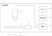
図2には、本発明の一実施形態の光学評価装置1の構成が示されている。光学評価装置1は、光照射装置10を構成部品(光照射器)として備え、物体11を光学的に評価する。物体11は、例えば、光沢を有する表面を有する。物体11は、例えば、表面が研磨された金属部品または樹脂部品でありうる。物体11の表面またはその近傍には、例えば、傷、色抜け、打痕等のように、多様な欠陥が存在しうる。 FIG. 2 shows the configuration of the optical evaluation device 1 according to the embodiment of the present invention. The optical evaluation device 1 includes a light irradiation device 10 as a component (light irradiator), and optically evaluates the object 11. The object 11 has, for example, a glossy surface. The object 11 can be, for example, a metal part or a resin part whose surface has been polished. Various defects such as scratches, color loss, dents, etc. may exist on or near the surface of the object 11.

光学評価装置1は、物体11の被検査領域の画像を取得し、その画像を処理して得られる処理画像を評価することにより、物体11の表面上の欠陥を検出しうる。また、光学評価装置1は、欠陥の検出結果に基づいて、例えば、物体11を良品または不良品に分類しうる。光学評価装置1は、図示されていないが、物体11を所定の位置に搬送する不図示の搬送装置(例えば、コンベアやロボット、スライダ、手動ステージなど)を備えうる。 The optical evaluation device 1 can detect defects on the surface of the object 11 by acquiring an image of the area to be inspected of the object 11 and evaluating the processed image obtained by processing the image. Further, the optical evaluation device 1 can classify the object 11 into a non-defective product or a defective product, for example, based on the defect detection result. Although not shown, the optical evaluation device 1 may include a transfer device (for example, a conveyor, a robot, a slider, a manual stage, etc.) (not shown) that conveys the object 11 to a predetermined position.

光学評価装置1は、物体11に光を照射することによって物体11を照明する光照射装置10と、光照射装置10を介して物体11を撮像する撮影部(カメラ)12とを備えうる。撮像部12は、複数の遮光部101の間の複数の開口部107を介して物体11を撮像する。撮像部12は、例えばCCDイメージセンサまたはCMOSイメージセンサ等のように、複数の画素が2次元状に配置されたイメージセンサ(エリアセンサ)と、物体11の像をイメージセンサの撮像面に形成する光学系とを含みうる。エリアセンサを採用することにより、ラインセンサを採用する場合よりも、物体11の広い範囲について高速に評価を行うことができる。 The optical evaluation device 1 may include a light irradiation device 10 that illuminates the object 11 by irradiating the object 11 with light, and a photographing unit (camera) 12 that captures the object 11 via the light irradiation device 10. The image pickup unit 12 takes an image of the object 11 through a plurality of openings 107 between the plurality of light-shielding portions 101. The image pickup unit 12 forms an image sensor (area sensor) in which a plurality of pixels are arranged two-dimensionally, such as a CCD image sensor or a CMOS image sensor, and an image of an object 11 on the image pickup surface of the image sensor. It may include an optical system. By adopting the area sensor, it is possible to evaluate a wide range of the object 11 at a higher speed than in the case of adopting the line sensor.

光学評価装置1は、駆動部13を備えている。駆動部13は、光照射装置10(複数の遮光部101および複数の光照射部102)を複数の遮光部101の各々の長さ方向(Y方向)と交差する方向(典型的には、X方向)に移動させる。図2に示された例では、駆動部13は、光照射装置10の全体を移動させるが、複数の遮光部101および複数の光照射部102が可動体に設けられている場合には、駆動部13は、該可動体だけを移動させてもよい。 The optical evaluation device 1 includes a drive unit 13. The drive unit 13 has a direction (typically, X) at which the light irradiation device 10 (a plurality of light-shielding units 101 and a plurality of light irradiation units 102) intersects the length direction (Y direction) of each of the plurality of light-shielding units 101. Move in the direction). In the example shown in FIG. 2, the drive unit 13 moves the entire light irradiation device 10, but when the plurality of light-shielding units 101 and the plurality of light irradiation units 102 are provided on the movable body, the drive unit 13 is driven. The unit 13 may move only the movable body.

光学評価装置1は、更に、制御部14を備えうる。制御部14は、例えば、FPGA(Field Programmable Gate Arrayの略。)などのPLD(Programmable Logic Deviceの略。)、又は、ASIC(Application Specific Integrated Circuitの略。)、又は、プログラムが組み込まれた汎用又は専用のコンピュータ、又は、これらの全部または一部の組み合わせによって構成されうる。制御部14は、例えば、光照射装置10、撮像部12および駆動部13を相互に同期させて動作させる。制御部14は、例えば、光照射装置10が一定の速度で移動するように駆動部13を制御しながら、撮像部12に一定の時間間隔でトリガー信号を送信し、N枚の画像(N≧3)を撮像させる。ただし、このような構成に限定されるものではなく、例えば、手動で駆動部13を操作して光照射装置10を移動させた後、マニュアルトリガーで撮像部12に撮像を実行させてもよい。 The optical evaluation device 1 may further include a control unit 14. The control unit 14 is, for example, a PLD (abbreviation for Programmable Logic Device) such as FPGA (abbreviation for Field Programmable Gate Array), or an ASIC (application specific integrated circuit) or a general-purpose program, or an abbreviation for an ASIC. Or it may consist of a dedicated computer, or a combination of all or part of these. The control unit 14 operates, for example, the light irradiation device 10, the image pickup unit 12, and the drive unit 13 in synchronization with each other. For example, the control unit 14 transmits a trigger signal to the image pickup unit 12 at regular time intervals while controlling the drive unit 13 so that the light irradiation device 10 moves at a constant speed, and N images (N ≧). 3) is imaged. However, the configuration is not limited to this, and for example, the drive unit 13 may be manually operated to move the light irradiation device 10, and then the image pickup unit 12 may perform imaging by a manual trigger.

光学評価装置1は、更に、画像処理部15およびディスプレイ16を備えうる。画像処理部15は、撮像部12によって撮像された複数(N枚)の画像に基づいて物体11を評価する。画像処理部15と制御部14は、一体化されてもよい。画像処理部15は、例えば、プログラムが組み込まれた汎用又は専用のコンピュータによって構成されうる。撮像部12によって撮像された画像は、ケーブル等の不図示の転送路または通信路を介して画像処理部15に転送されうる。 The optical evaluation device 1 may further include an image processing unit 15 and a display 16. The image processing unit 15 evaluates the object 11 based on a plurality of (N images) images captured by the image pickup unit 12. The image processing unit 15 and the control unit 14 may be integrated. The image processing unit 15 may be configured by, for example, a general-purpose or dedicated computer in which a program is incorporated. The image captured by the image pickup unit 12 can be transferred to the image processing unit 15 via a transfer path (not shown) such as a cable or a communication path.

撮像部12が撮像を行う撮像期間(露光期間)は、駆動部13が光照射装置10を移動させている移動期間内に設定される。換言すると、駆動部13が光照射装置10を移動させている状態で撮像部12が撮像を行う。露光期間は、撮像部12が光電変換によって発生した電荷を蓄積する期間、即ち電荷蓄積期間である。このような動作は、複数の遮光部101および複数の周期要素103によって形成される周波数成分のうち複数の周期要素103の周期Pよりも短い周期を有する周波数成分(高次の周波数成分)を低減するために有利である。以下、図3を参照しながら、この理由を説明する。 The imaging period (exposure period) in which the imaging unit 12 performs imaging is set within the moving period in which the driving unit 13 is moving the light irradiation device 10. In other words, the image pickup unit 12 takes an image while the drive unit 13 is moving the light irradiation device 10. The exposure period is a period in which the image pickup unit 12 accumulates the electric charge generated by the photoelectric conversion, that is, the electric charge accumulation period. Such an operation performs a frequency component (higher-order frequency component) having a period shorter than the period Po of the plurality of periodic elements 103 among the frequency components formed by the plurality of light-shielding portions 101 and the plurality of periodic elements 103. It is advantageous to reduce. Hereinafter, the reason for this will be described with reference to FIG.

図3(a)には、光照射装置10が静止した状態において撮像部12によって観察される複数の遮光部101の透過率分布が示されている。横軸がX座標、縦軸が透過率(撮像部12の露光期間における光量(輝度の時間積分値)と等価)を表す。ライン状の複数の遮光部101が中心間隔(周期)Pで配置されていることから、透過率分布は矩形波状となる。 FIG. 3A shows the transmittance distribution of the plurality of light-shielding portions 101 observed by the image pickup unit 12 in a state where the light irradiation device 10 is stationary. The horizontal axis represents the X coordinate, and the vertical axis represents the transmittance (equivalent to the amount of light (time integral value of luminance) in the exposure period of the imaging unit 12). Since the plurality of line-shaped light-shielding portions 101 are arranged at the center spacing (period) P m , the transmittance distribution has a rectangular wavy shape.

図3(b)には、光照射装置10がPだけ走査されている間に撮像部12が露光を続けた場合に撮像部12によって観察される複数の遮光部101の透過率分布(実線)が示されている。横軸がX座標、縦軸が透過率(撮像部12の露光期間における光量(輝度の時間積分値)と等価)を表す。図3(b)には、比較のため、図3(a)の透過率分が破線で示されている。光照射装置10がPだけ走査されている間に撮像部12が露光を続けることで、撮像部12によって観察される複数の遮光部101の透過率分布が平滑化され、上辺が略均一透過率を有する台形状の分布となる。 FIG. 3B shows the transmittance distribution (solid line) of the plurality of light-shielding portions 101 observed by the image pickup unit 12 when the image pickup unit 12 continues exposure while the light irradiation device 10 is scanned by P m . )It is shown. The horizontal axis represents the X coordinate, and the vertical axis represents the transmittance (equivalent to the amount of light (time integral value of luminance) in the exposure period of the imaging unit 12). In FIG. 3 (b), the transmittance of FIG. 3 (a) is shown by a broken line for comparison. By continuing the exposure of the imaging unit 12 while the light irradiation device 10 is scanned by P m , the transmittance distribution of the plurality of light-shielding units 101 observed by the imaging unit 12 is smoothed, and the upper side is substantially uniformly transmitted. It becomes a trapezoidal distribution with a rate.

図3(c)には、光照射装置10が静止した状態において撮像部12によって観察される複数の光照射部102の輝度分布が示されている。横軸がX座標、縦軸が輝度(撮像部12の露光期間における光量(輝度の時間積分値)と等価)を表す。ライン状の複数の光照射部102が周期Pを形成するように配置されていることから、輝度分布は、間隔が一定でない矩形波状となる。 FIG. 3C shows the luminance distribution of the plurality of light irradiation units 102 observed by the image pickup unit 12 in a state where the light irradiation device 10 is stationary. The horizontal axis represents the X coordinate, and the vertical axis represents the luminance (equivalent to the amount of light (the time integral value of the luminance) in the exposure period of the imaging unit 12). Since the plurality of line-shaped light irradiation units 102 are arranged so as to form a period Po , the luminance distribution has a rectangular wavy shape in which the intervals are not constant.

図3(d)には、光照射装置10がPだけ走査されている間に撮像部12が露光を続けた場合に撮像部12によって観察される複数の光照射部102の輝度分布(実線)が示されている。横軸がX座標、縦軸が輝度(撮像部12の露光期間における光量(輝度の時間積分値)と等価)を表す。図3(d)には、比較のため、図3(c)の透過率分布が破線で示されている。光照射装置10がPだけ走査されている間に撮像部が露光を続けることで、撮像部12によって観察される複数の光照射部102の輝度分布も平滑化される。ただし、複数の遮光部101の間隔Pよりも複数の光照射部102(複数の周期要素103)が形成する周期Pが大きい(この例では、PがPの4倍)ため、輝度分布は単一の台形ではなく台形波状となる。 FIG. 3D shows the luminance distribution (solid line) of the plurality of light irradiation units 102 observed by the image pickup unit 12 when the image pickup unit 12 continues the exposure while the light irradiation device 10 is scanned by P m . )It is shown. The horizontal axis represents the X coordinate, and the vertical axis represents the luminance (equivalent to the amount of light (the time integral value of the luminance) in the exposure period of the imaging unit 12). In FIG. 3 (d), the transmittance distribution in FIG. 3 (c) is shown by a broken line for comparison. By continuing the exposure of the image pickup unit while the light irradiation device 10 is scanned by P m , the luminance distribution of the plurality of light irradiation units 102 observed by the image pickup unit 12 is also smoothed. However, since the period Po formed by the plurality of light irradiation units 102 (plural period elements 103) is larger than the distance P m of the plurality of light-shielding portions 101 (in this example, Po is four times P m ). The brightness distribution is not a single trapezoid but a trapezoidal wave.

以上のように、光照射装置10を静止させて撮像部12によって撮像を行った場合、撮像部12によって観察される複数の遮光部101の透過率分布および複数の光照射部102(複数の周期要素103)の輝度分布には周期Pの周波数成分が含まれる。一方、光照射装置10を走査させながら撮像部12によって撮像を行った場合、周期Pの周波数成分、即ち高次の周波数成分を低減することができる。高次の周波数成分を低減することで、後ほど説明する処理画像における輝度(画素値)の均一性を改善することができる。 As described above, when the light irradiation device 10 is stationary and the image pickup unit 12 performs imaging, the transmittance distribution of the plurality of light-shielding units 101 observed by the image pickup unit 12 and the plurality of light irradiation units 102 (plural periods). The luminance distribution of element 103) includes a frequency component having a period of P m . On the other hand, when image pickup is performed by the image pickup unit 12 while scanning the light irradiation device 10, the frequency component having a period P m , that is, the higher-order frequency component can be reduced. By reducing the high-order frequency component, it is possible to improve the uniformity of the luminance (pixel value) in the processed image described later.

図3には、光照射装置10がPだけ走査されている間に撮像部12が露光を続けた場合において撮像部12によって観察される複数の遮光部101の透過率分布および複数の光照射部102の輝度分布が示されている。しかし、これは一例に過ぎず、撮像部12の撮像期間(露光期間)中の光照射装置10の移動量をPと同じにすることは必須ではない。ただし、撮像期間(露光期間)中の光照射装置10の移動量は、複数の周期要素103の中心間隔Pと幅Wとの差P-W(即ち、P-(n×P)よりも小さくすることが望ましい。これは、撮像期間中の光照射装置10の移動量がP-Wよりも大きいと、複数の光照射部102(複数の周期要素103)の輝度分布においてコントラストが高い画像(波形)が得られないためである。 FIG. 3 shows the transmittance distribution of the plurality of light-shielding portions 101 and the plurality of light irradiations observed by the image pickup unit 12 when the image pickup unit 12 continues the exposure while the light irradiation device 10 is scanned by P m . The luminance distribution of unit 102 is shown. However, this is only an example, and it is not essential that the amount of movement of the light irradiation device 10 during the imaging period (exposure period) of the imaging unit 12 is the same as P m . However, the amount of movement of the light irradiation device 10 during the imaging period (exposure period) is the difference between the center spacing Po and the width Wo of the plurality of periodic elements 103 Po - Wo (that is, Po- (n ×). It is desirable to make it smaller than P m ). This is because when the amount of movement of the light irradiation device 10 during the imaging period is larger than PoWo , the plurality of light irradiation units 102 (plural period elements 103) This is because an image (waveform) with high contrast cannot be obtained in the brightness distribution.

高次の周波数成分をより低減するためには、撮像部12が撮像(露光)と画像の転送とを並行して実行できる機能(オーバーラップ機能)を有していることが有利である。オーバーラップ機能がある撮像部12であれば、画像の転送に要する時間にも撮像を行うことが可能であり、より高い平滑化効果が得られる。 In order to further reduce higher-order frequency components, it is advantageous that the image pickup unit 12 has a function (overlap function) capable of performing image pickup (exposure) and image transfer in parallel. If the image pickup unit 12 has an overlap function, it is possible to perform imaging even during the time required for image transfer, and a higher smoothing effect can be obtained.

複数の周期要素103の各々を構成する光照射部102の個数が2以上である場合、各周期要素103では、それを構成する光照射部102が周期Pで配置されていることが望ましい。つまり、各周期要素103は、周期Pで連続的に配置されたn個の光照射部102で構成されていることが望ましい。これは、光照射装置10を走査させながら撮像部12の露光を続けた場合に、光照射部102の輝度分布に望ましくない周波数成分(周期P以外の周波数成分)が生じることを避けるためである。望ましくない周波数成分は、以下で説明する処理画像に悪影響を及ぼす可能性がある。 When the number of light irradiation units 102 constituting each of the plurality of periodic elements 103 is two or more, it is desirable that the light irradiation units 102 constituting each of the periodic elements 103 are arranged with a period P m . That is, it is desirable that each periodic element 103 is composed of n light irradiation units 102 continuously arranged with a periodic Pm. This is to prevent unwanted frequency components (frequency components other than period Po ) from occurring in the luminance distribution of the light irradiation unit 102 when the exposure of the image pickup unit 12 is continued while scanning the light irradiation device 10. be. Undesirable frequency components can adversely affect the processed image described below.

また、複数の周期要素103の幅W(即ち、n×P)と周期Pとの比(W/P)(デューティ比)は、1/4以上かつ3/4以下であることが好ましい。即ち、1/4≦(n×P)/P≦3/4という条件を満たすことが好ましい。これは、この条件を満たす場合、撮像部12によって観察される複数の光照射部102の輝度分布に生じる望ましくない周波数成分(周期P以外の周波数成分)が十分に小さいためである。また、同様の観点から、複数の遮光部101のデューティ比(WLB/P)および光照射部102のデューティ比(WLI/P)は、40%以下または60%以上であることが好ましい。ただし、デューティ比を大きくすると、遮光部101によって撮像部12の光学系の瞳の一部が遮光されることにより、解像度が低下する可能性がある。それを考慮すると、複数の遮光部101のデューティ比(WLB/P)および光照射部102のデューティ比(WLI/P)は、40%以下であることが好ましい。 Further, the ratio ( Wo / Po ) (duty ratio) of the width Wo (that is, n × P m ) of the plurality of periodic elements 103 to the periodic Po is 1/4 or more and 3/4 or less. Is preferable. That is, it is preferable to satisfy the condition of 1/4 ≦ (n × P m ) / P o ≦ 3/4. This is because, when this condition is satisfied, the undesired frequency component (frequency component other than the period Po ) generated in the luminance distribution of the plurality of light irradiation units 102 observed by the image pickup unit 12 is sufficiently small. From the same viewpoint, the duty ratio (W LB / P m ) of the plurality of light-shielding portions 101 and the duty ratio (W LI / P m ) of the light irradiation unit 102 may be 40% or less or 60% or more. preferable. However, if the duty ratio is increased, a part of the pupil of the optical system of the imaging unit 12 is shielded by the light-shielding unit 101, which may reduce the resolution. Considering this, the duty ratio (W LB / P m ) of the plurality of light-shielding portions 101 and the duty ratio (W LI / P m ) of the light irradiation unit 102 are preferably 40% or less.

図4には、光学評価装置1によって実行される検査方法の流れが示されている。この検査方法は、制御部14によって制御される。図4は、参照しながら物体11の表面の欠陥の検査する例を説明する。まず、工程S11では、制御部14は、駆動部13に、光照射装置10の走査(移動)を開始させる。工程S12では、制御部14は、駆動部13によって走査されている状態で、光照射装置10を発光させ(物体11に光を照射させ)、撮像部12が撮像を行わせる。これにより、撮像部12によってi番目の画像I(x,y)が撮像される。この動作は、i=1~Nまで繰り返され、その結果、合計のN枚N枚(N≧3)の画像が撮像される。(x,y)は、画像における画素の位置(座標値)を示す。 FIG. 4 shows the flow of the inspection method executed by the optical evaluation device 1. This inspection method is controlled by the control unit 14. FIG. 4 describes an example of inspecting a defect on the surface of the object 11 with reference to it. First, in step S11, the control unit 14 causes the drive unit 13 to start scanning (moving) the light irradiation device 10. In step S12, the control unit 14 causes the light irradiation device 10 to emit light (irradiates the object 11 with light) while being scanned by the drive unit 13, and the image pickup unit 12 causes the image pickup unit 12 to perform imaging. As a result, the i-th image I i (x, y) is imaged by the image pickup unit 12. This operation is repeated from i = 1 to N, and as a result, a total of N N images (N ≧ 3) are captured. (X, y) indicates the position (coordinate value) of the pixel in the image.

工程S14では、制御部14は、駆動部13に光照射装置10の走査を停止させる。工程S15では、画像処理部15に、工程S12の繰り返しによって得られたN枚の画像を処理させ、欠陥の検出のために用いる処理画像を生成させる。工程S16では、制御部14は、工程S15で得られた処理画像に基づいて、物体11の表面上の欠陥を検出する。 In step S14, the control unit 14 causes the drive unit 13 to stop scanning the light irradiation device 10. In the step S15, the image processing unit 15 is made to process N images obtained by repeating the step S12 to generate a processed image used for detecting defects. In step S16, the control unit 14 detects defects on the surface of the object 11 based on the processed image obtained in step S15.

処理画像の一例は、位相が2πΔX/Pラジアンでシフトする周波数成分の振幅画像である。ここで、ΔX(i=1,2,…N)は、i番目の画像を撮像する際の、基準位置に対する光照射装置10の位置である。光照射装置10の位置がΔXの場合、複数の周期要素103の位相は、2πΔX/Pラジアンで表される。光照射装置10を走査させながら一定の光量で発光させ、撮像部12で撮像(露光)を行った場合、ΔXは、露光期間中の光照射装置10の平均位置である。ΔXは、既知であれば任意の大きさに設定することができる。ただし、2πの整数倍だけ互いに異なる位相は同値であることから、ΔX≠ΔX+nPとなるような光照射装置10の位置で撮像が行われうる。 An example of a processed image is an amplitude image of a frequency component whose phase shifts in 2πΔX i / Po radians. Here, ΔX i (i = 1, 2, ... N) is the position of the light irradiation device 10 with respect to the reference position when the i-th image is captured. When the position of the light irradiation device 10 is ΔX i , the phases of the plurality of periodic elements 103 are represented by 2πΔX i / Po radians. When the light irradiation device 10 is scanned to emit light with a constant amount of light and the image pickup unit 12 performs imaging (exposure), ΔX i is the average position of the light irradiation device 10 during the exposure period. ΔX i can be set to any size as long as it is known. However, since the phases that differ from each other by an integral multiple of 2π have the same value, imaging can be performed at the position of the light irradiation device 10 such that ΔX n ≠ ΔX m + nP o .

光照射装置10の位置がP/Nの間隔となる条件で、N枚の画像を撮像した場合、ΔXは、式(1)で表される(ここでは、1番目の画像を撮像した位置を基準位置とする)。 When N images are imaged under the condition that the position of the light irradiation device 10 is the interval of Po / N, ΔX i is represented by the equation (1) (here, the first image is imaged). The position is used as the reference position).

ΔX=(P/N)×(i-1)
・・・(1)
この場合、振幅画像A(x,y)は、式(2)により算出できる。
ΔX i = ( Po / N) × (i-1)
... (1)
In this case, the amplitude image A (x, y) can be calculated by the equation (2).

Figure 0007061036000001
・・・(2)
Figure 0007061036000001
... (2)

光照射装置10を移動させると、光沢を有する物体11の表面上に写り込んだ複数の光照射部102の像が移動することにより、撮像部12の各画素では、入射光の輝度が変化する。物体11の表面のうち正常な光沢を有する部分では、光照射装置10の移動により輝度が大きく変化するため、輝度の振幅の値は大きくなる。一方、傷および表面荒れなど、散乱性の欠陥がある部分では、鏡面反射光以外にも散乱光が発生する。物体11の表面で光が散乱されると、表面上に写り込んだ複数の光照射部102の像がぼやけるため、強度の明暗の差が小さくなり、振幅の値も小さくなる。例えば、完全拡散面では光の散乱角度分布は入射光の角度に依存しなくなるため、複数の光照射部102で台形波状のパターンを物体11に投影しても、光照射装置10の位置によらず輝度は常に一定となり、振幅はゼロとなる。このため、振幅画像では正常部は明るく、欠陥部は暗く可視化される。したがって、振幅画像では表面性状として散乱性の度合いを評価することができ、傷および表面荒れなど、散乱性の欠陥の情報を得ることができる。 When the light irradiation device 10 is moved, the images of the plurality of light irradiation units 102 reflected on the surface of the glossy object 11 move, so that the brightness of the incident light changes in each pixel of the image pickup unit 12. .. In the portion of the surface of the object 11 having normal luster, the brightness changes greatly due to the movement of the light irradiation device 10, so that the value of the amplitude of the brightness becomes large. On the other hand, scattered light is generated in addition to specularly reflected light in a portion having a scattering defect such as a scratch or a rough surface. When light is scattered on the surface of the object 11, the images of the plurality of light irradiation units 102 reflected on the surface are blurred, so that the difference in intensity is small and the amplitude value is also small. For example, on a completely diffused surface, the light scattering angle distribution does not depend on the angle of the incident light, so even if a trapezoidal wavy pattern is projected onto the object 11 by the plurality of light irradiation units 102, it depends on the position of the light irradiation device 10. The brightness is always constant and the amplitude is zero. Therefore, in the amplitude image, the normal part is bright and the defective part is dark. Therefore, in the amplitude image, the degree of scattering property can be evaluated as the surface texture, and information on scattering defects such as scratches and surface roughness can be obtained.

処理画像の別の例は位相画像である。位相画像θ(x,y)は、式(3)により算出できる。 Another example of a processed image is a phase image. The phase image θ (x, y) can be calculated by the equation (3).

Figure 0007061036000002
・・・(3)
Figure 0007061036000002
... (3)

式(3)では、位相は-π~πの値で算出されるため、それ以上に位相が変化する場合は、位相画像では非連続な位相の飛びが発生する。このような場合には、位相接続(位相アンラップ)が必要となる。 In the equation (3), the phase is calculated by a value of −π to π. Therefore, when the phase changes further, a discontinuous phase jump occurs in the phase image. In such a case, phase connection (phase unwrap) is required.

位相画像では、表面性状として物体11の表面の傾きを評価することができる。したがって、位相画像では、打痕、面倒れ、表面の凹みのような緩やかな形状変化に起因する欠陥の情報を得ることができる。 In the phase image, the inclination of the surface of the object 11 can be evaluated as the surface texture. Therefore, in the phase image, it is possible to obtain information on defects caused by gradual shape changes such as dents, chamfering, and surface dents.

位相接続(位相アンラップ)には、種々のアルゴリズムが提案されているが、画像のノイズが大きい場合には、位相接続に失敗する場合がある。位相接続を回避するための手法として、位相の代わりに位相差(位相の微分に相当)を算出してもよい。位相差Δθ(x,y)及びΔθ(x,y)は、式(4)により算出できる。 Various algorithms have been proposed for phase connection (phase unwrap), but if the image noise is large, the phase connection may fail. As a method for avoiding the phase connection, the phase difference (corresponding to the differential of the phase) may be calculated instead of the phase. The phase difference Δθ x (x, y) and Δθ y (x, y) can be calculated by the equation (4).

Figure 0007061036000003
・・・(4)
Figure 0007061036000003
... (4)

更なる処理画像の例は、平均画像である。平均画像Iave(x,y)は、式(5)により算出できる。 An example of a further processed image is an average image. The average image I ave (x, y) can be calculated by the equation (5).

Figure 0007061036000004
・・・(5)
Figure 0007061036000004
... (5)

平均画像では、表面性状として反射率の分布を評価できる。したがって、平均画像では、色抜け、汚れ、吸収性の異物など、正常な部分に対して反射率に違いがある欠陥の情報を得ることができる。 In the average image, the distribution of reflectance can be evaluated as the surface texture. Therefore, in the average image, it is possible to obtain information on defects having different reflectances with respect to normal parts such as color loss, stains, and absorbent foreign substances.

以上のように、処理画像によって、光学的に評価可能な表面性状が異なる。したがって、各処理画像で可視化される欠陥も異なるため、これらの処理画像を組み合わせることによって、多様な欠陥を画像上に可視化することができる。 As described above, the surface texture that can be optically evaluated differs depending on the processed image. Therefore, since the defects visualized in each processed image are also different, various defects can be visualized on the image by combining these processed images.

ところで、図3(b)、(d)では、光照射装置10を走査しながら撮像部12が露光を続けた場合に撮像部12によって観察される複数の遮光部101の透過率分布、複数の光照射部102の輝度分布が示された。しかし、複数の遮光部101の位置と複数の光照射部102の位置とは互いに独立してはいない。よって、光照射装置10を走査させながら露光した場合の画像は、厳密には図3(b)の複数の光照射部102の透過率分布と図3(d)の複数の光照射部102の輝度分布との積とはならない。結果として、画像には高次の周波数成分が含まれ、物体11の正常な領域でも、平均画像、振幅画像、位相画像に周期的な強度の不均一性が生じうる。これらの画像の強度(画素値)に不均一性が存在すると、物体11の表面上の欠陥の検出精度を低下させる可能性がある。 By the way, in FIGS. 3 (b) and 3 (d), the transmittance distributions of the plurality of light-shielding portions 101 observed by the image pickup unit 12 when the image pickup unit 12 continues the exposure while scanning the light irradiation device 10, and a plurality of. The brightness distribution of the light irradiation unit 102 is shown. However, the positions of the plurality of light-shielding portions 101 and the positions of the plurality of light irradiation portions 102 are not independent of each other. Therefore, strictly speaking, the image when the light irradiation device 10 is exposed while scanning is the transmittance distribution of the plurality of light irradiation units 102 in FIG. 3 (b) and the plurality of light irradiation units 102 in FIG. 3 (d). It is not the product of the brightness distribution. As a result, the image contains higher frequency components, and even in the normal region of the object 11, periodic intensity non-uniformity can occur in the average image, the amplitude image, and the phase image. The presence of non-uniformity in the intensities (pixel values) of these images may reduce the accuracy of detecting defects on the surface of the object 11.

図5には、複数の周期要素103の中心間隔Pと複数の遮光部101の中心間隔Pとの比(P/P)に対して、画像上に生じる強度(画素値)の不均一性を計算した結果を示す。両対数プロットにおいて、P/Pが大きくなると、強度の不均一性が直線的に低下することが分かる。したがって、すべての遮光部101に対して光照射部102が設けられた場合(P=P)では、画像上に大きな強度の不均一性が発生すること分かる。また、画像の均一性を向上させるためにはできるだけP/Pを大きくした方がよいことが分かる。このため、複数の周期要素103の中心間隔Pは、複数の遮光部101の中心間隔Pの2倍以上、できれば8倍以上とすることが好ましい。 FIG. 5 shows the intensity (pixel value) generated on the image with respect to the ratio ( Po / P m) of the center spacing Po of the plurality of periodic elements 103 and the center spacing P m of the plurality of light-shielding portions 101. The result of calculating the non-uniformity is shown. In the log-log plot, it can be seen that as Po / P m increases, the intensity non-uniformity decreases linearly. Therefore, it can be seen that when the light irradiation unit 102 is provided for all the light shielding units 101 ( Po = P m ), a large intensity non-uniformity occurs on the image. Further, it can be seen that it is better to increase Po / P m as much as possible in order to improve the uniformity of the image. Therefore, the center spacing Po of the plurality of periodic elements 103 is preferably twice or more, preferably eight times or more, the center spacing P m of the plurality of light-shielding portions 101.

一方で、複数の遮光部101の中心間隔Pを小さくし過ぎると、光の回折作用によって像がぼやけ、解像力の低下を招く。光照射装置10によって照射される光の波長をλとしたとき、遮光部101による1次回折光の角度θは、式(6)で表される。 On the other hand, if the center spacing Pm of the plurality of light- shielding portions 101 is made too small, the image is blurred due to the diffraction action of light, and the resolving power is lowered. When the wavelength of the light emitted by the light irradiating device 10 is λ, the angle θ of the primary diffracted light by the light-shielding portion 101 is represented by the equation (6).

Figure 0007061036000005
・・・(6)
Figure 0007061036000005
... (6)

複数の遮光部101が配置された面と物体11の表面との間の距離をDとすると、1次回折光によって物体11の表面上で2Dtanθのボケが発生する。許容されるボケの量をBとしたとき、複数の遮光部101の中心間隔Pは、(2Dλ/B)よりも大きくすることすることが必要である。 Assuming that the distance between the surface on which the plurality of light-shielding portions 101 are arranged and the surface of the object 11 is D, the primary diffracted light causes a blur of 2Dtan θ on the surface of the object 11. When the allowable amount of blur is B, the center spacing Pm of the plurality of light-shielding portions 101 needs to be larger than ( 2Dλ / B).

一方で、P/Pが大きく、Pの値も大きいと、複数の周期要素103の中心間隔Pも大きな値となる。この場合、駆動部13によって光照射装置10を移動させる距離が大きくなるので、光学評価装置1の大型化を招きうる。また、複数の周期要素103の中心間隔Pが大きいと、振幅画像において散乱の程度が低い(指向性が高い)散乱性の欠陥を位相画像において検出しづらくなる。P/Pを過度に大きくしても画像の強度の不均一性はノイズなどに埋もれて改善しないことから、複数の周期要素103の中心間隔Pは、複数の遮光部101の中心間隔Pの256倍以下とすることが好ましい。 On the other hand, when Po / P m is large and the value of P m is also large, the center spacing Po of the plurality of periodic elements 103 also becomes a large value. In this case, the distance for moving the light irradiation device 10 by the drive unit 13 becomes large, which may lead to an increase in the size of the optical evaluation device 1. Further, when the center spacing Po of the plurality of periodic elements 103 is large, it becomes difficult to detect a scattering defect with a low degree of scattering (high directivity) in the amplitude image in the phase image. Since the non-uniformity of the image intensity is buried in noise and does not improve even if Po / P m is excessively increased, the center spacing Po of the plurality of periodic elements 103 is the center spacing of the plurality of light-shielding portions 101. It is preferably 256 times or less of P m .

実施例1の光学評価装置1では、複数の遮光部101の中心間隔Pが0.5mm、複数の周期要素103の中心間隔Pが8mm、各周期要素103の幅Wが4mmである。したがって、P/Wは16、周期要素103のデューティ比(W/P)は50%である。また、遮光部101の幅WLBは0.2mm(デューティ比(WLB/P)は40%)、光照射部102の幅WLIは0.1mm(デューティ比(WLI/P)は20%)である。 In the optical evaluation device 1 of the first embodiment, the center spacing P m of the plurality of light-shielding portions 101 is 0.5 mm, the center spacing Po of the plurality of periodic elements 103 is 8 mm, and the width W o of each periodic element 103 is 4 mm. .. Therefore, P m / W o is 16, and the duty ratio (W o / P o ) of the periodic element 103 is 50%. The width W LB of the light shielding portion 101 is 0.2 mm (duty ratio (W LB / P m ) is 40%), and the width W LI of the light irradiation unit 102 is 0.1 mm (duty ratio (W LI / P m )). Is 20%).

光学評価装置1は、複数の周期要素103の位相が互いに異なる位置で16枚の画像を撮像する。駆動部13は、10mm/秒の速度で光照射装置10を走査し、撮像部12は、50msの露光期間および撮像間隔で撮像を行う。この条件では、各画像の露光期間における光照射装置10の移動量は、0.5mmである。また、駆動部13による光照射装置10の加減速に要する時間などを除き、16枚の画像の撮像のための動作は0.8秒で完了する。 The optical evaluation device 1 captures 16 images at positions where the phases of the plurality of periodic elements 103 are different from each other. The drive unit 13 scans the light irradiation device 10 at a speed of 10 mm / sec, and the image pickup unit 12 performs imaging at an exposure period of 50 ms and an imaging interval. Under this condition, the amount of movement of the light irradiation device 10 during the exposure period of each image is 0.5 mm. Further, the operation for capturing 16 images is completed in 0.8 seconds, excluding the time required for acceleration / deceleration of the light irradiation device 10 by the drive unit 13.

実施例2の光学評価装置では、複数の遮光部101の中心間隔Pが1mm、複数の周期要素103の中心間隔Pが12mm、各周期要素103の幅Wは6mmである。したがって、P/Wは12、周期要素103のデューティ比(W/P)は50%である。また、遮光部101の幅WLBは0.3mm(デューティ比(WLB/P)は30%)、光照射部102の幅WLIは0.2mm(デューティ比(WLI/P)は20%)である。 In the optical evaluation device of the second embodiment, the center spacing P m of the plurality of light-shielding portions 101 is 1 mm, the center spacing Po of the plurality of periodic elements 103 is 12 mm, and the width W o of each periodic element 103 is 6 mm. Therefore, P m / W o is 12, and the duty ratio (W o / P o ) of the periodic element 103 is 50%. The width W LB of the light shielding portion 101 is 0.3 mm (duty ratio (W LB / P m ) is 30%), and the width W LI of the light irradiation unit 102 is 0.2 mm (duty ratio (W LI / P m )). Is 20%).

光学評価装置1は、複数の周期要素103の位相が互いに異なる位置で9枚の画像を撮像する。駆動部13は、22.2mm/秒の速度で光照射装置10を走査し、撮像部12は、60msの露光期間および撮像間隔で画像を行う。この条件では、角井画像の露光期間における光照射装置10の移動量は、1.33mmである。また、駆動部13による光照射装置10の加減速に要する時間などを除き、9枚の画像の撮像のための動作は0.54秒で完了する。 The optical evaluation device 1 captures nine images at positions where the phases of the plurality of periodic elements 103 are different from each other. The drive unit 13 scans the light irradiation device 10 at a speed of 22.2 mm / sec, and the image pickup unit 12 captures images with an exposure period of 60 ms and an imaging interval. Under this condition, the amount of movement of the light irradiation device 10 during the exposure period of the Kakui image is 1.33 mm. Further, the operation for capturing nine images is completed in 0.54 seconds, except for the time required for acceleration / deceleration of the light irradiation device 10 by the drive unit 13.

本実施形態の光照射装置10は、撮像部12は、光照射装置10の複数の開口部107を介して物体11を撮像することができる。したがって、光照射装置10と撮像部12とを同軸上に配置すること、換言すると、物体11と撮像部12との間に光照射装置10を配置することができる。このため、光照射装置10を物体11の近傍に配置することができ、小型の光照射装置10を使う場合においても、物体11の表面の広い範囲から撮像部12への正反射光が得られる。したがって、本実施形態の光照射装置10を用いた光学評価装置1によれば、物体11の表面の広い範囲を一括で光学的に評価することができる。特に、物体の表面が曲面である場合には、非透過型の光照射装置においては、物体から光照射装置が遠いと、物体の広い範囲から撮像部への正反射光を得るためには光照射装置が巨大になる。したがって、本実施形態による光照射装置10は、物体の表面が曲面である場合に特に有効である。また、本実施形態の光照射装置10によれば、複数の周期要素103の中心間隔Pを遮光部101の中心間隔Pの2倍以上とすることで、物体11の表面の評価に悪影響を及ぼす画像上の強度の不均一性を低減することができる。 In the light irradiation device 10 of the present embodiment, the image pickup unit 12 can image the object 11 through the plurality of openings 107 of the light irradiation device 10. Therefore, the light irradiation device 10 and the image pickup unit 12 can be arranged coaxially, in other words, the light irradiation device 10 can be arranged between the object 11 and the image pickup unit 12. Therefore, the light irradiation device 10 can be arranged in the vicinity of the object 11, and even when a small light irradiation device 10 is used, specularly reflected light can be obtained from a wide range of the surface of the object 11 to the image pickup unit 12. .. Therefore, according to the optical evaluation device 1 using the light irradiation device 10 of the present embodiment, it is possible to optically evaluate a wide range of the surface of the object 11 collectively. In particular, when the surface of the object is a curved surface, in a non-transmissive light irradiation device, if the light irradiation device is far from the object, light is required to obtain specularly reflected light from a wide range of the object to the image pickup unit. The irradiation device becomes huge. Therefore, the light irradiation device 10 according to the present embodiment is particularly effective when the surface of the object is a curved surface. Further, according to the light irradiation device 10 of the present embodiment, the center spacing Po of the plurality of periodic elements 103 is set to be at least twice the center spacing P m of the light-shielding portion 101, which adversely affects the evaluation of the surface of the object 11. It is possible to reduce the non-uniformity of the intensity on the image.

また、本実施形態の光照射装置10を用いた光学評価装置1は、物品製造方法(加工方法)の一工程として行う光学評価(光学検査)に用いることができる。例えば、加工されたワーク(被加工物)の表面を本実施形態の光学評価装置1を用いて光学的に評価し、その評価結果が閾値よりも良い結果であれば次の工程(を行う装置)に搬送し、閾値以下の悪い結果であれば再加工の工程(を行う装置)に搬送しても良い。つまり、本実施形態の光学評価装置1は、光学評価結果に応じて互いに異なる処理(次工程装置への搬送、再加工装置への搬送)を行う物品の製造方法に適用可能である。そして、本実施形態の光学評価装置1を用いれば、製造装置(加工装置)内部に大きな空間を必要とすることなく、光学評価工程を組み入れる(光学評価装置を組み込む)ことが可能となる。 Further, the optical evaluation device 1 using the light irradiation device 10 of the present embodiment can be used for optical evaluation (optical inspection) performed as one step of the article manufacturing method (processing method). For example, the surface of the processed work (workpiece) is optically evaluated using the optical evaluation device 1 of the present embodiment, and if the evaluation result is better than the threshold value, the next step (is performed). ), And if the result is bad below the threshold value, it may be transported to the reworking process (device that performs). That is, the optical evaluation device 1 of the present embodiment can be applied to a method of manufacturing an article that performs different processes (transportation to the next process device, transfer to the reprocessing device) according to the optical evaluation result. Then, by using the optical evaluation device 1 of the present embodiment, it is possible to incorporate the optical evaluation process (incorporate the optical evaluation device) without requiring a large space inside the manufacturing device (processing device).

1:光学評価装置、10:光照射装置、101:遮光部、102:光照射部、103:周期要素、11:物体、12:撮影部、13:駆動部、14:制御部、15:画像処理部 1: Optical evaluation device, 10: Light irradiation device, 101: Light-shielding unit, 102: Light irradiation unit, 103: Periodic element, 11: Object, 12: Imaging unit, 13: Drive unit, 14: Control unit, 15: Image Processing unit

Claims (14)

物体に光を照射する光照射装置であって、
一定の中心間隔で配置され、少なくとも部分的に光を遮断するライン状の複数の遮光部と、
前記物体に光を照射するように前記複数の遮光部のうちの一部の遮光部に対して重なるように配置されたライン状の複数の光照射部と、を含み、
前記複数の光照射部は、前記複数の遮光部の前記中心間隔の2倍以上の周期で周期的に配置された複数の周期要素を含む
ことを特徴とする光照射装置。
It is a light irradiation device that irradiates an object with light.
Multiple line-shaped light-shielding parts that are arranged at regular center intervals and block light at least partially,
Includes a plurality of line-shaped light irradiating portions arranged so as to overlap a part of the light-shielding portions of the plurality of light-shielding portions so as to irradiate the object with light.
The plurality of light irradiation units include a plurality of periodic elements that are periodically arranged at a cycle of twice or more the center spacing of the plurality of light-shielding portions.
A light irradiation device characterized by this.
記複数の周期要素の各々は、同じ個数の光照射部で構成される、
ことを特徴とする請求項1に記載の光照射装置。
Each of the plurality of periodic elements is composed of the same number of light irradiation units.
The light irradiation device according to claim 1.
前記個数が2以上であり、前記複数の周期要素の各々における前記光照射部の中心間隔が前記複数の遮光部の前記中心間隔と等しい、
ことを特徴とする請求項2に記載の光照射装置。
The number is 2 or more, and the center spacing of the light irradiation portion in each of the plurality of periodic elements is equal to the center spacing of the plurality of light-shielding portions.
The light irradiation device according to claim 2.
前記個数をn、前記複数の遮光部の前記中心間隔をP、前記周期をPとしたときに、
1/4≦(n×P)/P≦3/4
を満たすことを特徴とする請求項2又は3に記載の光照射装置。
When the number is n, the center spacing of the plurality of light-shielding portions is P m , and the period is Po .
1/4 ≤ (n x P m ) / P o ≤ 3/4
The light irradiation device according to claim 2 or 3, wherein the light irradiation device is characterized by satisfying the above conditions.
前記複数の光照射部の各々の幅は、前記複数の遮光部の各々の幅以下である、
ことを特徴とする請求項1乃至4のいずれか1項に記載の光照射装置。
The width of each of the plurality of light irradiation portions is equal to or less than the width of each of the plurality of light-shielding portions.
The light irradiation device according to any one of claims 1 to 4, wherein the light irradiation device is characterized.
前記複数の遮光部の各々の長さ方向と前記複数の遮光部が配置された方向とが互いに直交することを特徴とする請求項1乃至5のいずれか1項に記載の光照射装置。 The light irradiation device according to any one of claims 1 to 5, wherein the length direction of each of the plurality of light-shielding portions and the direction in which the plurality of light-shielding portions are arranged are orthogonal to each other. 光を透過する板部材を更に含み、
前記複数の遮光部および前記複数の光照射部は、前記板部材の主面の上に配置されている、
ことを特徴とする請求項1乃至6のいずれか1項に記載の光照射装置。
Further includes a plate member that transmits light,
The plurality of light-shielding portions and the plurality of light-irradiating portions are arranged on the main surface of the plate member.
The light irradiation device according to any one of claims 1 to 6, wherein the light irradiation device is characterized.
前記複数の光照射部は、前記複数の遮光部のうち前記複数の光照射部が重なるように配置された遮光部と前記主面との間に配置されている、
ことを特徴とする請求項7に記載の光照射装置。
The plurality of light irradiation units are arranged between the light shielding portion arranged so that the plurality of light irradiation portions overlap among the plurality of light shielding portions and the main surface.
The light irradiation device according to claim 7.
前記板部材の端面に対して光を照射する光源を更に含む、
ことを特徴とする請求項8に記載の光照射装置。
A light source that irradiates the end face of the plate member with light is further included.
The light irradiation device according to claim 8.
前記複数の光照射部の厚さは、前記複数の遮光部の前記中心間隔より小さい、
ことを特徴とする請求項1乃至9のいずれか1項に記載の光照射装置。
The thickness of the plurality of light irradiation portions is smaller than the center spacing of the plurality of light-shielding portions.
The light irradiation device according to any one of claims 1 to 9, wherein the light irradiation device is characterized.
請求項1に記載の光照射装置と、
前記光照射装置によって光が照射された前記物体を、前記複数の遮光部の間の開口部を介して撮像する撮像部と、
前記複数の遮光部および前記複数の光照射部を前記複数の遮光部の各々の長さ方向と交差する方向に移動させる駆動部と、
前記撮像部によって撮像された複数の画像に基づいて前記物体を評価する画像処理部と、
を備えることを特徴とする光学評価装置。
The light irradiation device according to claim 1 and
An image pickup unit that captures an image of the object irradiated with light by the light irradiation device through an opening between the plurality of light-shielding portions.
A drive unit that moves the plurality of light-shielding portions and the plurality of light-irradiating portions in a direction intersecting the length direction of each of the plurality of light-shielding portions.
An image processing unit that evaluates the object based on a plurality of images captured by the image pickup unit, and an image processing unit.
An optical evaluation device characterized by being provided with.
前記撮像部は、前記駆動部が前記複数の遮光部および前記複数の光照射部を移動させている状態で撮像を行う、
ことを特徴とする請求項11に記載の光学評価装置。
The imaging unit performs imaging in a state where the driving unit moves the plurality of light-shielding units and the plurality of light irradiation units.
The optical evaluation device according to claim 11.
記複数の周期要素の各々は、同じ個数の光照射部で構成され、
前記個数をn、前記複数の遮光部の前記中心間隔をP、前記周期をPとしたときに、
前記撮像部の露光期間において前記駆動部が前記複数の遮光部および前記複数の光照射部を移動させる距離が、P-(n×P)より小さい、
ことを特徴とする請求項12に記載の光学評価装置。
Each of the plurality of periodic elements is composed of the same number of light irradiation units.
When the number is n, the center spacing of the plurality of light-shielding portions is P m , and the period is Po .
The distance by which the driving unit moves the plurality of light-shielding portions and the plurality of light-irradiating portions during the exposure period of the imaging unit is smaller than Po − (n × P m ).
The optical evaluation device according to claim 12.
請求項11乃至13のいずれか1項に記載の光学評価装置を用いて物品の評価を行う工程と、
前記評価の結果に応じた処理を前記物品に対して行う工程と、
を含むことを特徴とする物品製造方法。
A step of evaluating an article using the optical evaluation device according to any one of claims 11 to 13.
A step of performing a process on the article according to the result of the evaluation, and
A method for manufacturing an article, which comprises.
JP2018126888A 2018-07-03 2018-07-03 Light irradiation device, optical evaluation device and article manufacturing method Active JP7061036B2 (en)

Priority Applications (3)

Application Number Priority Date Filing Date Title
JP2018126888A JP7061036B2 (en) 2018-07-03 2018-07-03 Light irradiation device, optical evaluation device and article manufacturing method
US16/454,542 US10686995B2 (en) 2018-07-03 2019-06-27 Light irradiation apparatus, optical evaluation apparatus, and article manufacturing method
CN201910591735.9A CN110672615A (en) 2018-07-03 2019-07-03 Light irradiation apparatus, optical evaluation apparatus, and article manufacturing method

Applications Claiming Priority (1)

Application Number Priority Date Filing Date Title
JP2018126888A JP7061036B2 (en) 2018-07-03 2018-07-03 Light irradiation device, optical evaluation device and article manufacturing method

Publications (3)

Publication Number Publication Date
JP2020008318A JP2020008318A (en) 2020-01-16
JP2020008318A5 JP2020008318A5 (en) 2021-07-29
JP7061036B2 true JP7061036B2 (en) 2022-04-27

Family

ID=69068612

Family Applications (1)

Application Number Title Priority Date Filing Date
JP2018126888A Active JP7061036B2 (en) 2018-07-03 2018-07-03 Light irradiation device, optical evaluation device and article manufacturing method

Country Status (3)

Country Link
US (1) US10686995B2 (en)
JP (1) JP7061036B2 (en)
CN (1) CN110672615A (en)

Families Citing this family (3)

* Cited by examiner, † Cited by third party
Publication number Priority date Publication date Assignee Title
IT201700099120A1 (en) * 2017-09-05 2019-03-05 Salvatore Lamanna LIGHTING SYSTEM FOR SCREEN OF ANY KIND
CN111561870B (en) * 2020-05-29 2021-10-08 神华准格尔能源有限责任公司 Method and system for acquiring outdoor plant phenotype data
CN112184706B (en) * 2020-10-29 2024-03-05 广东省电子技术研究所 Chip resistor silk screen appearance detection method and device, electronic equipment and storage medium

Citations (6)

* Cited by examiner, † Cited by third party
Publication number Priority date Publication date Assignee Title
JP2002109513A (en) 2000-09-28 2002-04-12 Toyota Motor Corp Coating defect detector and mask image preparing method
JP2002258763A (en) 2001-03-01 2002-09-11 Ohtsu Tire & Rubber Co Ltd :The Illuminator
JP2003098093A (en) 2001-09-25 2003-04-03 Ccs Inc Lighting system for examination
EP2272417A1 (en) 2009-07-10 2011-01-12 GE Inspection Technologies, LP Fringe projection system and method for a probe suitable for phase-shift analysis
JP2014002125A (en) 2012-06-21 2014-01-09 Fujitsu Ltd Inspection method and inspection device
JP2014059164A (en) 2012-09-14 2014-04-03 4D Sensor Inc Shape measurement device and shape measurement method

Family Cites Families (2)

* Cited by examiner, † Cited by third party
Publication number Priority date Publication date Assignee Title
US7476629B2 (en) * 2003-04-21 2009-01-13 Semiconductor Energy Laboratory Co., Ltd. Beam irradiation apparatus, beam irradiation method, and method for manufacturing thin film transistor
JP5853331B2 (en) * 2011-03-11 2016-02-09 株式会社ブイ・テクノロジー Laser irradiation apparatus and method for correcting bright spot of liquid crystal display panel using the same

Patent Citations (6)

* Cited by examiner, † Cited by third party
Publication number Priority date Publication date Assignee Title
JP2002109513A (en) 2000-09-28 2002-04-12 Toyota Motor Corp Coating defect detector and mask image preparing method
JP2002258763A (en) 2001-03-01 2002-09-11 Ohtsu Tire & Rubber Co Ltd :The Illuminator
JP2003098093A (en) 2001-09-25 2003-04-03 Ccs Inc Lighting system for examination
EP2272417A1 (en) 2009-07-10 2011-01-12 GE Inspection Technologies, LP Fringe projection system and method for a probe suitable for phase-shift analysis
JP2014002125A (en) 2012-06-21 2014-01-09 Fujitsu Ltd Inspection method and inspection device
JP2014059164A (en) 2012-09-14 2014-04-03 4D Sensor Inc Shape measurement device and shape measurement method

Non-Patent Citations (1)

* Cited by examiner, † Cited by third party
Title
FORTE, Paulo M.F. 外6名,"Exploring combined dark and bright field illumination to improve the detection of defects on specular surfaces",OPTICS AND LASERS IN ENGINEERING,2016年08月26日,Volume 88,Pages 120-128,<URL: https://doi.org/10.1016/j.optlaseng.2016.08.002 >

Also Published As

Publication number Publication date
US20200014835A1 (en) 2020-01-09
JP2020008318A (en) 2020-01-16
US10686995B2 (en) 2020-06-16
CN110672615A (en) 2020-01-10

Similar Documents

Publication Publication Date Title
JP3878023B2 (en) 3D measuring device
JP7061036B2 (en) Light irradiation device, optical evaluation device and article manufacturing method
JP5410092B2 (en) Apparatus and method for inspecting composite structures for inconsistencies
JP3878165B2 (en) 3D measuring device
WO2008123604A1 (en) Surface inspection device
KR101294915B1 (en) Micro-mirror device sorting method, micro-mirror device sorting apparatus, and maskless exposure apparatus
US10740890B2 (en) Image processing apparatus, method, and storage medium
KR101203210B1 (en) Apparatus for inspecting defects
US20180367722A1 (en) Image acquisition device and image acquisition method
JP2012242268A (en) Inspection device and inspection method
JP4808072B2 (en) Filter checkered plate, three-dimensional measuring device and illumination means
US20190132524A1 (en) Image generation method, image generation apparatus, and defect determination method using image generation method and image generation apparatus
JP5498708B2 (en) Appearance inspection apparatus and resin molded product manufacturing method
JP7010213B2 (en) Cylindrical surface inspection device and cylindrical surface inspection method
JP2007114125A (en) Method for inspecting film thickness irregularities
JP2008180578A (en) Cyclic pattern nonuniformity inspection device
JP2009222683A (en) Method and apparatus for surface inspection
JP2014169988A (en) Defect inspection device of transparent body or reflection body
JP5531405B2 (en) Periodic pattern unevenness inspection method and inspection apparatus
JP2008139126A (en) Flaw detector and flaw detection method
JP4743395B2 (en) Pitch unevenness inspection method and pitch unevenness inspection apparatus
KR20200068541A (en) Optical system for automated optical inspection
JP2012058029A (en) Periodic pattern inspection device
JP3405118B2 (en) Surface defect inspection equipment
JP2012150079A (en) Defect detection device for transparent member and defect detection method

Legal Events

Date Code Title Description
RD01 Notification of change of attorney

Free format text: JAPANESE INTERMEDIATE CODE: A7421

Effective date: 20210103

A521 Request for written amendment filed

Free format text: JAPANESE INTERMEDIATE CODE: A523

Effective date: 20210113

A521 Request for written amendment filed

Free format text: JAPANESE INTERMEDIATE CODE: A523

Effective date: 20210615

A621 Written request for application examination

Free format text: JAPANESE INTERMEDIATE CODE: A621

Effective date: 20210615

A977 Report on retrieval

Free format text: JAPANESE INTERMEDIATE CODE: A971007

Effective date: 20220304

TRDD Decision of grant or rejection written
A01 Written decision to grant a patent or to grant a registration (utility model)

Free format text: JAPANESE INTERMEDIATE CODE: A01

Effective date: 20220318

A61 First payment of annual fees (during grant procedure)

Free format text: JAPANESE INTERMEDIATE CODE: A61

Effective date: 20220415

R151 Written notification of patent or utility model registration

Ref document number: 7061036

Country of ref document: JP

Free format text: JAPANESE INTERMEDIATE CODE: R151