JP7055424B2 - Methods and equipment using an optical engine for photocuring of liquid polymers to form three-dimensional objects - Google Patents
Methods and equipment using an optical engine for photocuring of liquid polymers to form three-dimensional objects Download PDFInfo
- Publication number
- JP7055424B2 JP7055424B2 JP2019539903A JP2019539903A JP7055424B2 JP 7055424 B2 JP7055424 B2 JP 7055424B2 JP 2019539903 A JP2019539903 A JP 2019539903A JP 2019539903 A JP2019539903 A JP 2019539903A JP 7055424 B2 JP7055424 B2 JP 7055424B2
- Authority
- JP
- Japan
- Prior art keywords
- array
- lens
- led
- dimensional object
- lenses
- Prior art date
- Legal status (The legal status is an assumption and is not a legal conclusion. Google has not performed a legal analysis and makes no representation as to the accuracy of the status listed.)
- Active
Links
Images


Classifications
-
- B—PERFORMING OPERATIONS; TRANSPORTING
- B29—WORKING OF PLASTICS; WORKING OF SUBSTANCES IN A PLASTIC STATE IN GENERAL
- B29C—SHAPING OR JOINING OF PLASTICS; SHAPING OF MATERIAL IN A PLASTIC STATE, NOT OTHERWISE PROVIDED FOR; AFTER-TREATMENT OF THE SHAPED PRODUCTS, e.g. REPAIRING
- B29C64/00—Additive manufacturing, i.e. manufacturing of three-dimensional [3D] objects by additive deposition, additive agglomeration or additive layering, e.g. by 3D printing, stereolithography or selective laser sintering
- B29C64/10—Processes of additive manufacturing
- B29C64/106—Processes of additive manufacturing using only liquids or viscous materials, e.g. depositing a continuous bead of viscous material
- B29C64/124—Processes of additive manufacturing using only liquids or viscous materials, e.g. depositing a continuous bead of viscous material using layers of liquid which are selectively solidified
- B29C64/129—Processes of additive manufacturing using only liquids or viscous materials, e.g. depositing a continuous bead of viscous material using layers of liquid which are selectively solidified characterised by the energy source therefor, e.g. by global irradiation combined with a mask
-
- B—PERFORMING OPERATIONS; TRANSPORTING
- B29—WORKING OF PLASTICS; WORKING OF SUBSTANCES IN A PLASTIC STATE IN GENERAL
- B29C—SHAPING OR JOINING OF PLASTICS; SHAPING OF MATERIAL IN A PLASTIC STATE, NOT OTHERWISE PROVIDED FOR; AFTER-TREATMENT OF THE SHAPED PRODUCTS, e.g. REPAIRING
- B29C64/00—Additive manufacturing, i.e. manufacturing of three-dimensional [3D] objects by additive deposition, additive agglomeration or additive layering, e.g. by 3D printing, stereolithography or selective laser sintering
- B29C64/20—Apparatus for additive manufacturing; Details thereof or accessories therefor
- B29C64/264—Arrangements for irradiation
- B29C64/277—Arrangements for irradiation using multiple radiation means, e.g. micromirrors or multiple light-emitting diodes [LED]
-
- B—PERFORMING OPERATIONS; TRANSPORTING
- B33—ADDITIVE MANUFACTURING TECHNOLOGY
- B33Y—ADDITIVE MANUFACTURING, i.e. MANUFACTURING OF THREE-DIMENSIONAL [3-D] OBJECTS BY ADDITIVE DEPOSITION, ADDITIVE AGGLOMERATION OR ADDITIVE LAYERING, e.g. BY 3-D PRINTING, STEREOLITHOGRAPHY OR SELECTIVE LASER SINTERING
- B33Y30/00—Apparatus for additive manufacturing; Details thereof or accessories therefor
Description
本発明は、3Dプリンティングと通称されている三次元印刷またはプリンティングの分野、特に立体物(三次元物体)の形成のために液体ポリマーの光硬化を利用する3Dプリンティング装置で用いられる光エンジンに関する。 The present invention relates to the field of three-dimensional printing or printing, commonly referred to as 3D printing, particularly to optical engines used in 3D printing devices that utilize photocuring of liquid polymers for the formation of three-dimensional objects (three-dimensional objects).
〔関連出願の参照〕
本願は、2017年1月25日に出願された米国特許仮出願第62/450,470号、2017年7月11日に出願された米国特許仮出願第62/531,211号、2017年7月11日に出願された米国特許仮出願第62/531,276号、および2017年7月12日に出願された米国特許仮出願第62/531,461号ならびに2017年1月25日に出願された米国特許出願第15/415,688号の優先権主張出願である。
[Refer to related applications]
This application is based on US Patent Provisional Application No. 62 / 450,470 filed on January 25, 2017, US Patent Provisional Application No. 62 / 531,21 filed on July 11, 2017, July 2017. US Patent Provisional Application No. 62 / 531,276 filed on March 11, 2017, and US Patent Application No. 62 / 531,461 filed on July 12, 2017, and filed on January 25, 2017. This is a priority claim application of US Patent Application No. 15 / 415,688.
知られているように、光硬化による3Dプリンティングによる分野は、2つの基本的な技術、すなわち、約400nmのレーザ放出光が用いられて放出されたビームによって特殊なタンク内に入れられた光硬化性液体ポリマーを凝固させる光造形プリンティングおよびこの場合もまたタンク内に存在している光硬化性液体ポリマーをプロジェクタと同様な装置によって放出された光放射線に暴露させるDLP(ディジタル光加工)プリンティングを含むと言える。これら両方の技術によれば、プリンティングプロセスは、完成物体の形成まで物体の1つの層を別の層の後に作製することによって、すなわち、支持プレート(または取り出しプレート)に付着している第1の層を凝固させ、次に第1の層にくっついている第2の層を凝固させるなどすることによって進む。したがって、これらの技術によれば、形成されるべき立体物を表しているデータは、構築中の物体の横方向区分を表す一連の二次元層として組織化される。 As is known, the field of 3D printing by photocuring is two basic techniques: photocuring placed in a special tank by a beam emitted using laser emission light of about 400 nm. Includes stereolithography printing that solidifies the sex liquid polymer and DLP (digital photoprocessing) printing that also exposes the photocurable liquid polymer present in the tank to the light radiation emitted by a device similar to a projector. It can be said that. According to both of these techniques, the printing process is by creating one layer of the object after another layer until the formation of the finished object, i.e., a first attachment to the support plate (or removal plate). The process proceeds by solidifying the layers and then solidifying the second layer that is attached to the first layer. Therefore, according to these techniques, the data representing the three-dimensional object to be formed is organized as a series of two-dimensional layers representing the lateral divisions of the object under construction.
SLAおよびDLPタイプのいずれかの機械を必要とする場合のあるボトムアップ方法によれば、物体を取り出すためのプレートは、物体が層ごとに形成されているときに、タンクの底部から上方に動く。基本的なボトムアップ方法は、次のステップから成り、すなわち次の通りである。
a.構築されるべき物体の3Dモデルをコンピュータソフトウェアで層の順序づけられた連続体として表し、その厚さは、採用した技術、液体ポリマーの不透明度、ポリマーとともに用いられる触媒の量、得られるべき精度、および提供される機械の特性に従って定められ、通常、この厚さは、50~200ミクロンであるが、いずれの場合においても、3Dモデルは、別々のかつ有限数の層の連続体として表され、
b.ポリマーの第1の層のそれ自体へのくっつきを容易にすることができる材料から成る取り出しプレートが第1の層から所定の距離を置いたところまで動き、そして光ビーム(SLAまたはDLP)が第1の層を凝固させるのを待ち、次に、取り出しプレートが形成されたばかりの層がタンクのベースから外れるのに十分な距離(通常、約1mm)だけ上昇し、次に同一距離だけ下降し、第2の層の形成のために所定の距離よりも短い距離だけ下降するなどし、ついには物体全体が形成されるようにする。
According to bottom-up methods that may require either SLA or DLP type machines, the plate for ejecting the object moves upward from the bottom of the tank as the object is formed layer by layer. .. The basic bottom-up method consists of the following steps, ie:
a. The 3D model of the object to be constructed is represented by computer software as an ordered continuum of layers, the thickness of which is the technique adopted, the opacity of the liquid polymer, the amount of catalyst used with the polymer, the accuracy to be obtained, And determined according to the characteristics of the machine provided, usually this thickness is 50-200 microns, but in each case the 3D model is represented as a series of separate and finite number of layers.
b. A take-out plate made of a material that can facilitate the attachment of the first layer of polymer to itself moves to a predetermined distance from the first layer, and a light beam (SLA or DLP) is first. Wait for the layer 1 to solidify, then the layer on which the take-out plate has just been formed rises by a distance sufficient (usually about 1 mm) to disengage from the base of the tank, then descends by the same distance. The second layer is formed by descending a distance shorter than a predetermined distance so that the entire object is finally formed.
基本的なボトムアップ方法の改良例が2016年10月3日に出願された本出願人の国際出願PCT/IT2016/000225号明細書に記載されており、この国際出願は、2015年10月2日に出願されたイタリア国特許出願第102015000057527号明細書の優先権主張出願である。この特許出願では、液体ポリマーを硬化させるために用いられる電磁スペクトル放射線に対して透明でありかつ硬化が行われるタンクの底部と形成中の物体の層との間に存在する自己潤滑性サブストレータム(またはメンブレン)が記載されている。メンブレンは、潤滑性物質の層を次第に放出し、それにより、メンブレンの上方に浮いた状態で存在する液体ポリマーがメンブレン上で硬化することができ、かくして形成中の物体層とタンクベースとの吸引効果および付着性を減少させる。光源、例えばDLPプロジェクタは、液体ポリマーとのメンブレンのインターフェースのところに像焦点面を有する。液体ポリマーの光硬化は、投影された像に従ってこのインターフェースのところで起こる。構築中の物体の成長がそれにより容易になる。 An improved example of the basic bottom-up method is described in the applicant's international application PCT / IT2016 / 00225, which was filed on October 3, 2016, and this international application is on October 2, 2015. It is a priority claim application of the Italian patent application No. 102015000057527 filed on the same day. In this patent application, a self-lubricating substrate that is transparent to the electromagnetic spectrum radiation used to cure the liquid polymer and exists between the bottom of the tank where the curing takes place and the layer of the object being formed. (Or membrane) is described. The membrane gradually releases a layer of lubricating material, which allows the liquid polymer floating above the membrane to cure on the membrane, thus attracting the forming object layer to the tank base. Reduces effectiveness and adhesion. A light source, such as a DLP projector, has an image focal plane at the interface of the membrane with the liquid polymer. Photocuring of the liquid polymer occurs at this interface according to the projected image. It facilitates the growth of the object being constructed.
かかる構成は受け入れ可能なプリンティング速度を見越しているが、かかる構成は、構築中の物体に限定されたx‐y解像度(例えば、75ミクロンのオーダ)をもたらすに過ぎない。さらに、液体ポリマーを硬化させるのに相当な光強度が必要なので、DLPプロジェクタは、焦点面の近くに位置決めされなければならず、それにより液体ポリマーの硬化を行わせることができる面積が制限される(例えば、120×90mmのオーダまで)。作業空間へのDLPプロジェクタのこの近接性はまた、焦点面内に光収差およびディストーション(歪曲)をもたらす。 Such configurations anticipate acceptable printing rates, but such configurations only provide xy resolution (eg, on the order of 75 microns) limited to the object under construction. In addition, since significant light intensity is required to cure the liquid polymer, the DLP projector must be positioned close to the focal plane, which limits the area in which the liquid polymer can be cured. (For example, up to an order of 120 x 90 mm). This proximity of the DLP projector to the workspace also results in photoaberration and distortion within the focal plane.
本発明の実施形態は、DLPプロジェクタを平行光源(collimated light source)で置き換え、そしてLCDディスプレイを結像プラットホームとして用いることによって例えば上述したような欠点を解決する。光源は、像を作るためにLCDパネルを通る放射線(radiation)の平行光束流をもたらし、この平行光束流は、一実施形態では、400~700nmの波長範囲内にあり、特に410nmである。LCDパネルは、複数のアドレス指定可能な画素を含み、これら画素は、入射放射線に対して個別的に透明または不透明に作られるのが良い。マトリックス中の結晶のうちの透明な結晶を通る入射放射線の作用効果により、ディスプレイ表面上に像が作られる。マトリックスの個々の結晶は、代表的には表示のための像のビットマップ(または他の)バージョンが提供されるプロセッサまたは他のコントローラの制御下において、電圧をそれぞれの結晶に印加しまたは印加しないことによって透明にまたは不透明に作られる。 Embodiments of the present invention solve, for example, the above-mentioned drawbacks by replacing the DLP projector with a collimated light source and using an LCD display as an imaging platform. The light source provides a parallel light flux of radiation through the LCD panel to create an image, which in one embodiment is in the wavelength range of 400-700 nm, particularly 410 nm. The LCD panel contains a plurality of addressable pixels, which are preferably made transparent or opaque individually to incident radiation. An image is created on the surface of the display by the action and effect of incident radiation passing through the transparent crystals of the crystals in the matrix. Each crystal in the matrix applies or does not apply voltage to each crystal, typically under the control of a processor or other controller that provides a bitmap (or other) version of the image for display. By making it transparent or opaque.
平行光源は、個々の光エミッタのアレイ、特に、放射線を400~700nmの波長で、特に410nmの波長で放出するよう構成された発光ダイオード(LED)源のアレイによって作られる。平行光源は、バッフルのアレイおよびレンズのアレイをさらに含むのが良く、バッフルは、LED源のアレイ中の個々のLED源の各々のビーム幅をレンズアレイに含まれる一レンズのほぼ直径に制限するよう配置され、レンズのアレイは、LED源のアレイから焦点距離1つ分のところに配置される。 Parallel light sources are made up of an array of individual light emitters, in particular an array of light emitting diode (LED) sources configured to emit radiation at wavelengths of 400-700 nm, especially 410 nm. The parallel light source may further include an array of baffles and an array of lenses, which limits the beam width of each of the individual LED sources in the array of LED sources to approximately the diameter of one lens contained in the lens array. The array of lenses is arranged at a focal length of one from the array of LED sources.
本発明のこれらの実施形態および追加の実施形態を以下にさらに説明する。 These embodiments and additional embodiments of the present invention will be further described below.
いま、本発明の実施形態を示す添付の図面を参照して一例によりかつ本発明の範囲を限定しないで、本発明について説明する。 Now, the present invention will be described by way of example and without limiting the scope of the present invention with reference to the accompanying drawings showing embodiments of the present invention.
本出願人の国際出願PCT/IT2016/000225号明細書では、自己潤滑性サブストレータムを採用しながら立体物または三次元物体の形成のために液体ポリマーを光硬化させる方法および装置が記載されている。これら方法および装置は、吸引効果(形成中の物体の層とこの下に位置決めされたタンクのベースとの間の真空に起因して生じる)を減少させまたはなくし、形成中の層とタンクベースとの付着性を減少させまたはなくし、上述の作用効果によって生じる機械的応力を減少させ、そして従来型解決策と比較して、立体物を非常に短い時間で形成するプロセスを提供する。特に、立体物の形成のための光硬化を行うかかる方法および装置では、タンクのベースと光硬化性液体ポリマーとの間にメンブレンを介在させ、このメンブレンは、関心のある電磁スペクトルに対して透明であり、かつ潤滑性物質の層を徐々に放出することができ、それにより適切にドープされたポリマーが潤滑性物質の層上に浮いた状態のままで凝固することができる。 The applicant's international application PCT / IT2016 / 00225 describes a method and apparatus for photocuring a liquid polymer for the formation of a three-dimensional or three-dimensional object while adopting a self-lubricating substrate. There is. These methods and devices reduce or eliminate the suction effect (caused by the vacuum between the layer of object being formed and the base of the tank positioned beneath it), with the layer being formed and the tank base. It provides a process of reducing or eliminating the adhesiveness of the material, reducing the mechanical stress caused by the effects described above, and forming a three-dimensional object in a very short time compared to conventional solutions. In particular, in such methods and devices that perform photocuring for the formation of solids, a membrane is interposed between the base of the tank and the photocurable liquid polymer, which is transparent to the electromagnetic spectrum of interest. And the layer of lubricating material can be gradually released so that the appropriately doped polymer can solidify while floating on the layer of lubricating material.
かかる構成の一例が図1に示されている。DLPプロジェクタ10がタンク(図示せず)のベースのところに設けられたホウケイ酸ガラスの層14を通って光束流12を生じさせる。ホウケイ酸ガラスの上にはメンブレン16が位置している。メンブレン16は、2016年10月3日に出願された国際出願PCT/IT2016/000225号明細書に詳細に記載されており、この国際出願は、2015年10月2日に出願されたイタリア国特許出願102015000057527号の優先権主張出願であり、このイタリア国出願を参照により引用し、その記載内容を本明細書の一部とする。概要を説明すると、メンブレン16は、DLPプロジェクタ10からの電磁スペクトル放射線に対して透明でありかつ潤滑性物質の層を徐々に放出することができる自己潤滑性サブストレータムであり、それにより、メンブレンの上方に浮いた状態で位置する液体ポリマー18がメンブレン上で硬化することができ、かくして吸引効果を減少させるとともに形成中の物体層とタンクベースとの付着性をなくす。DLPプロジェクタ10は、液体ポリマー18とのメンブレン16のインターフェースのところに像焦点面20を有する。液体ポリマーの光硬化は、投影された像に従ってこのインターフェースのところで起こり、構築中の物体の成長は、それにより容易になる。液体ポリマーには紫外線触媒(DLPプロジェクタによって生じる光束流の帯域幅において敏感である)および潤滑性物質が適切にドープされるのが良い。この構成は、迅速な物体成長(厚さ200ミクロンの層について1.8min/cmのオーダのプリンティング速度で)を可能にするが、x‐y解像度を制限する(例えば、75ミクロン)。さらに、相当な光強度が液体ポリマーを硬化させるのに必要なので、DLPプロジェクタは、作業空間の近くに位置決めされなければならず、それにより液体ポリマーの硬化を行わせることができる面積が制限される(例えば、120×90mmのオーダまで)。作業空間へのDLPプロジェクタのこの近接性はまた、焦点面内に光収差およびディストーション(歪曲)をもたらす。
An example of such a configuration is shown in FIG. A
本発明の実施形態は、DLPプロジェクタの使用をなくし、これに代えて約410nmの波長(または、より一般的に言って、400~700nmの波長範囲内にある波長)で電磁線を放出する平行光源を用いることによってこれらの欠点を解決する。光源は、一実施形態では、出力が個々のビームディレクタ(beam director)(またはバッフル)によって拘束されるとともにレンズアレイによって平行にされる発光ダイオード(LED)のアレイからなる。その結果得られる平行光ビームは、液体ポリマーを収容したタンク内にかつ上述のメンブレンの下に配置された液晶ディスプレイ(LCD)を照明するために用いられる。LCDは、印刷されるべき物体の断面の像の表示を提供するようコンピュータ制御下にあり、その結果、平行光ビームは、入射放射線の波長に対して不透明になっていないLCDの部分を通過してLCDの真上に位置する装置の作業空間内の液体ポリマーの光硬化を生じさせる。この構成は、x‐y平面内に光収差またはディストーションのない高い解像度(例えば、約50ミクロン以下のオーダで、一実施形態では、約30ミクロン)をもたらし、他方、迅速なプリンティング速度(例えば、約2~2.5秒で200ミクロンのオーダのプリンティング厚さ)を保つ。 Embodiments of the invention eliminate the use of DLP projectors and instead emit parallels at wavelengths of about 410 nm (or, more generally, wavelengths in the wavelength range of 400-700 nm). These drawbacks are solved by using a light source. The light source, in one embodiment, consists of an array of light emitting diodes (LEDs) whose outputs are constrained by individual beam directors (or baffles) and paralleled by a lens array. The resulting parallel light beam is used to illuminate a liquid crystal display (LCD) located in a tank containing a liquid polymer and under the membrane described above. The LCD is under computer control to provide an image of the cross section of the object to be printed, so that the parallel light beam passes through a portion of the LCD that is not opaque to the wavelength of the incident radiation. Causes photocuring of the liquid polymer in the work space of the device located directly above the LCD. This configuration provides high resolution (eg, on the order of about 50 microns or less, about 30 microns in one embodiment) with no photoaberration or distortion in the xy plane, while a rapid printing rate (eg, about 30 microns). Keep the printing thickness on the order of 200 microns in about 2 to 2.5 seconds).
図2は、この構成の一例を示している。光源32が像39を作るためにLCDパネル33を通る放射線の平行光束流38をもたらし、この平行光束流は、一実施形態では、400~700nmの波長範囲内にあり、特に410nmである。LCDパネルは、液晶マトリックス36をサンドイッチした2つの偏光層34,35を有する。液晶マトリックスは、複数のアドレス指定可能な画素を含み、これら画素は入射放射線に対して個別的に透明にまたは不透明に作られるのが良い。マトリックス中の結晶のうちの透明な結晶を通る入射放射線の作用効果により、ディスプレイ表面37上に像39が作られる。マトリックス36の個々の結晶は、代表的には表示のための像のビットマップ(または他の)バージョンが提供されるプロセッサまたは他のコントローラの制御下において、電圧をそれぞれの結晶に印加しまたは印加しないことによって透明にまたは不透明に作られる。一実施形態では、LCDディスプレイ33は、840dpiの解像度を有するのが良い。
FIG. 2 shows an example of this configuration. The
平行光源のための光の波長は、LCDディスプレイの偏光子が典型的にはUVフィルタとして働くので、光の可視範囲のエッジで選択される。3Dプリンティング用に用いられる形式の多くの光硬化可能なポリマー(レジンとも呼ばれる)がUV帯で硬化する。したがって、LCD結像装置を用いることにより、紫外線がLCDディスプレイの偏光子によって濾波除去されるので従来型システムでは問題が生じる。同時に、可視帯で硬化するレジンは、典型的には、像平面内に約50ミクロン以下のx‐y解像度を達成するようには使用できない。これとは異なり、これらシステムは、典型的には、100ミクロンのオーダの解像度を達成する。したがって、本発明の実施形態で用いられるレジンは、約370nmの中心波長で硬化可能であるが、平行光源の好ましい波長である410nmでは良好な硬化特性を依然としてもたらす。 The wavelength of light for a parallel light source is selected at the edge of the visible range of light, as the splitter of the LCD display typically acts as a UV filter. Many of the forms of photocurable polymers (also called resins) used for 3D printing cure in the UV band. Therefore, the use of an LCD imaging device causes problems in conventional systems because UV light is filtered out by the polarizing elements of the LCD display. At the same time, resins that cure in the visible band cannot typically be used to achieve xy resolution of about 50 microns or less in the image plane. In contrast, these systems typically achieve resolutions on the order of 100 microns. Therefore, the resin used in the embodiments of the present invention can be cured at a center wavelength of about 370 nm, but still provides good curing properties at 410 nm, which is the preferred wavelength of parallel light sources.
上述したように、好ましい光源は、平行光源であり、これは、個々の光エミッタのアレイによって作られる。これは、点光源がレジン(少なくとも、十分に広い領域にわたってではない)の硬化を生じさせるのに十分なエネルギーを生じさせない傾向があり、さらに、図3Aに示されているようにズーム効果に起因したディストーションを生じさせるからである。点光源、例えば単一のUV LED40が光硬化性配列体中のLCDディスプレイ33を照明するため用いられる場合(単純化のため、この配列体のホウケイ酸ガラス14およびメンブレン16だけが示されている)、元の像41がメンブレン16の頂面上の像平面のところで拡大状態42になる。これは、拡大像がそのエッジのところで不規則になる傾向がありかつ誤ったサイズのものとなるので、満足のゆくものではない。さらに、像平面のところの光エネルギーは、その領域全体にわたって非一様であり、したがって、硬化時間は、像の中心とそのエッジとの間ではばらつきがある。
As mentioned above, the preferred light source is a parallel light source, which is made up of an array of individual light emitters. This is because point sources tend not to generate enough energy to cause the resin (at least not over a large enough area) to cure, and also due to the zoom effect as shown in FIG. 3A. This is because it causes the distortion. When a point light source, such as a
しかしながら、光源のアレイを用いることは、それ自体必ず難題である。源のアレイは、レジンの光硬化を生じさせるとともに像領域全体にわたって光エネルギーの分布を一層一様にするのに十分なエネルギーを達成するために必要とされるが、図3Bに示されているように、アレイ中の個々の源が各々像平面内にそれ自体の像(拡大状態)を生じさせるのでシャドー効果を生じさせる。個々のLED源43‐1,43‐2,43‐3のアレイ43がホウケイ酸ガラス14とメンブレン16との間に設けられたLEDディスプレイ33を照明する。かくして、これら源の各々は、メンブレン16と光硬化性レジン(図示せず)とのインターフェースのところで像平面のところでLCDディスプレイ33上にそれ自体のそれぞれの像の表示44‐1,44‐2,44‐3を生じさせる。これら像は、各々、拡大されて互いにオーバーラップし、その結果、シャドー効果および他の望ましくない像硬化が生じる。単一の物体(例えば、LCD像)上に入射する2つの光源に関するシャドー効果の一例が図4に示されている。
However, using an array of light sources is always a challenge in itself. An array of sources is required to cause photocuring of the resin and to achieve sufficient energy to make the distribution of light energy more uniform over the image region, as shown in FIG. 3B. As such, each individual source in the array produces its own image (enlarged state) in the image plane, thus producing a shadow effect. An
平行光源を用いると、図5に示されているように、これらシャドー効果がなくなる。平行光束流45がバッフル47およびコリメートレンズ48のアレイを用いて個々のLED46‐1,46‐2,46‐3のアレイ46によって作られる。バッフル47は、個々のLED源46‐1,46‐2,46‐3の各々のビーム幅をアレイ48中に用いられているレンズのほぼ直径に制限するよう配置されている。レンズのアレイは、各LED源から焦点距離1つ分だけ離れて配置され、各LED源はまた、互いに焦点距離1つ分だけ離されて配置されるのが良く、それゆえ、バッフルは、かかる離隔距離に対応するよう寸法決めされる。本発明の一実施形態では、LED源の9×12アレイが用いられる。これは、図6に示されており、図6は、LEDのアレイ46、各々がLEDの各々にそれぞれ対応したバッフル47、レンズ48のアレイ、LED1つ当たり1つのレンズ、およびLCDディスプレイ33を分解組立図で示しており、これらにより、印刷されるべき像がもたらされる。図5に戻ってこれを参照すると、レンズのアレイ48により生じた平行光は、LCD33からの像が光硬化性液体ポリマー(図示せず)の底面の真下でメンブレン16の頂部インターフェース上に投影されたときにその元のサイズを保持するようにする。LCDは、印刷されるべき物体の断面の像の表示を提供するようコンピュータ制御下にあり、その結果、平行光ビームは、入射放射線の波長に対して不透明になっていないLCDの部分を通過してLCDの真上に位置する装置の作業空間内の液体ポリマーの光硬化を生じさせる。この構成は、x‐y平面内に光収差またはディストーションのない高い解像度(例えば、約50ミクロン以下のオーダで、一実施形態では、約30ミクロン)をもたらし、他方、迅速なプリンティング速度を保つ。
The use of parallel light sources eliminates these shadow effects, as shown in FIG. A parallel
本発明の種々の実施形態では、LED源ビーム幅は、中心からのこれらの角変位全体の約90%以上に拘束される。幾つかの実施形態では、これは、レンズのアレイ中に用いられているレンズの焦点距離1つ分のバッフル付きLED相互間の距離に一致している。本発明の一実施形態では、平行光源は、約410nmで250mW/cm2の光束を生じさせ、840dpiのLCDディスプレイを用いてディストーションなしで約30ミクロンのx‐y解像度で約2~2.5秒以内の厚さ200ミクロン層の印刷を可能にする。アレイの個々のLED源は、レンズアレイに属するレンズの焦点距離のところでレンズから間隔を置いて位置し、それゆえ、バッフルは各々四方が焦点距離1つ分である。 In various embodiments of the invention, the LED source beam width is constrained to about 90% or more of all these angular displacements from the center. In some embodiments, this corresponds to the distance between the baffled LEDs for one focal length of the lenses used in the array of lenses. In one embodiment of the invention, the parallel light source produces a luminous flux of 250 mW / cm 2 at about 410 nm and is about 2 to 2.5 at an xy resolution of about 30 microns without distortion using an 840 dpi LCD display. Allows printing of 200 micron thick layers within seconds. The individual LED sources of the array are located at a distance from the lens at the focal length of the lens belonging to the lens array, so the baffles are each one focal length on each side.
図7に示されているように、一実施形態では、平行光源は、ポリマーが硬化を生じている作業領域全体にわたって十分なかつ適度に一貫した光束を保証するよう、幅が約20°以下であり、すなわちその中心軸線から半径方向に約10°以内であり、より具体的には約15°以内であり、すなわちその中心軸線から半径方向に約7.5°以内の空間放射パターンをなして各源LED源から放出された光を拘束するよう構成されている。 As shown in FIG. 7, in one embodiment, the parallel light source is about 20 ° or less in width to ensure a sufficient and reasonably consistent luminous flux over the entire working area where the polymer is curing. That is, within about 10 ° in the radial direction from the central axis, more specifically within about 15 °, that is, in a spatial radiation pattern within about 7.5 ° in the radial direction from the central axis. It is configured to constrain the light emitted from the source LED source.
本発明の別の実施形態は、放射線への暴露によって液体ポリマーを光硬化させることによって立体物の形成をもたらし、この放射線は、多周波LED源のアレイ、バッフルのアレイ、およびレンズのアレイで構成された平行光源によって提供される。バッフルは、LEDのアレイ中の個々のLED源の各々のビーム幅を制限し、レンズのアレイは、LED源のアレイから焦点距離1つ分のところに配置される。平行光源は、複数のフィルタを有する液晶ディスプレイをさらに含み、複数のフィルタの各フィルタは、LED源からの放出放射線の波長に対応している。 Another embodiment of the invention results in the formation of a three-dimensional object by photocuring a liquid polymer upon exposure to radiation, which radiation comprises an array of multi-frequency LED sources, an array of baffles, and an array of lenses. Provided by parallel light sources. The baffle limits the beam width of each of the individual LED sources in the array of LEDs, and the array of lenses is located one focal length from the array of LED sources. The parallel light source further includes a liquid crystal display having a plurality of filters, and each filter of the plurality of filters corresponds to the wavelength of the emitted radiation from the LED source.
図8は、ディスプレイ表面37のところに像を作るようLCDパネル33′を通る放射線の平行光束流を提供する光源32′の一例を示している。LCDパネル33′は、液晶マトリックス36をサンドイッチした2つの偏光層34,35を有する。液晶マトリックスは、複数のアドレス指定可能な画素を含み、これら画素は入射放射線に対して個別的に透明にまたは不透明に作られるのが良い。マトリックス中の結晶のうちの透明な結晶を通る入射放射線の作用効果により、ディスプレイ表面37上に像39が作られる。マトリックス36の個々の結晶は、代表的には表示のための像のビットマップ(または他の)バージョンが提供されるプロセッサまたは他のコントローラの制御下において、電圧をそれぞれの結晶に印加しまたは印加しないことによって透明にまたは不透明に作られる。この実施例では、偏光層34,35は、多源LEDアレイ46′を構成するLED62a~62nからの紫外線に対して透明である。
FIG. 8 shows an example of a light source 32'that provides a parallel luminous flux flow of radiation through the LCD panel 33' to form an image at the
加うるに、LCDパネル33′内には組をなす2つまたは3つ以上のUVフィルタ66が含まれている。UVフィルタ66は、各々が多源LEDアレイ46′のLEDからの入射放射線の幅の狭い周波数範囲を濾波除去するよう狭い帯域幅を有するよう設計されている。UVフィルタ66は、この実施例で示されているようにまたはLCDパネル内のどこかほかの場所で液晶マトリックス36と上側偏光フィルム35との間に位置決めされるのが良い。好ましくは、多源LEDアレイ46′を構成するLED62a~62nは各々、2つまたは3つ以上の幅の狭い帯域幅の光を放出し、UVフィルタ66は、かかる帯域幅に合わされており、その結果、LEDの放出光の各波長について対応のUVフィルタが存在するようになっている。
In addition, the LCD panel 33'contains two or more UV filters 66 in pairs. The UV filters 66 are each designed to have a narrow bandwidth to filter out a narrow frequency range of incident radiation from the LEDs of the multi-source LED array 46'. The UV filter 66 is preferably positioned between the
上述したように、液晶マトリックス36は、複数のアドレス指定可能な画素を含み、これらアドレス指定可能な画素は、入射放射線に対して個々に透明または不透明に作られるのが良い。一実施形態では、能動型(例えば、TFT)LCDパネルが用いられるが、他の場合、受動型(例えば、STN)LCDパネルが用いられるのが良い。液晶マトリックスの各セグメントは、LED62a~62nからの入射光に対してゲートとして働く。UVフィルタ66と一緒に、LCDパネルは、画素ごとの条件に基づいて、入射紫外線の特定の波長を通しまたは遮断する。例えば、LED62a~62nが各々、光を波長UVa,UVb,UVcで放出することができる場合、液晶マトリックスのセグメントを透明であるようにまたは透明ではないように制御することによって、ディスプレイ表面のところの像の各「画素」を波長UVa,UVb,またはUVcのうちの1つであるようにまたはこれらの2つまたは3つ以上の組み合わせであるように制御するのが良い。これは、赤色‐緑色‐青色LCDディスプレイがカラー画像を提供する仕方と類似している。光を多数の別々のUV波長で放出するLEDの例は、カリフォルニア州サンジョゼ所在のエルイーディー・エンジン・インコーポレイテッド(LED Engin, Inc.)から入手できるLEDのLZ4シリーズである。
As described above, the
バッフル47は、個々のLED源62a~62nのビーム幅を中心からのこれらの角変位全体のほんの何分の一かに拘束する。幾つかの実施形態では、バッフルは、互いにレンズ48のアレイ中に用いられているレンズの焦点距離1つ分のところに心出しされている。さらに、アレイの個々のLED源62a~62nは、レンズアレイ48に属するレンズの焦点距離のところでレンズから間隔を置いて位置し、それゆえ、バッフル47は各々四方が焦点距離1つ分である。
The
光エンジン32′は、ディスプレイ表面のところに像を作るようLCDパネル33′を通って放射線の平行光束流を1つまたは2つ以上の波長で提供する。LED源に関する光の種々の波長は、作製中の三次元物品を形成する元となるポリマーレジン中への種々の添加物を可能にするよう選択されるのが良い。3Dプリンティング用に用いられる形式の多くの光硬化可能なポリマー(レジンとも呼ばれる)がUV帯で硬化する。互いに異なる波長で敏感な硬化剤を導入することにより、入射放射線を適切に濾波することによって、作製中の物体の互いに異なる構造的特性を達成することができる。 The optical engine 32'provides a parallel luminous flux flow of radiation at one or more wavelengths through the LCD panel 33'to form an image at the surface of the display. The different wavelengths of light with respect to the LED source may be selected to allow different additives in the polymer resin from which they form the three-dimensional article being made. Many of the forms of photocurable polymers (also called resins) used for 3D printing cure in the UV band. By properly filtering the incident radiation by introducing sensitive curing agents at different wavelengths, different structural properties of the object being manufactured can be achieved.
例えば、硬化剤の中には波長UVaで敏感なものがあれば、波長UVbで敏感なものもある。適当に選択されたUVフィルタ66を維持するとともに上述した仕方でLCDパネル33′の画素に光を波長UVa,UVbで選択的に通しまたは通さないようにすることによって、互いに異なる硬化剤をポリマーレジンとのメンブレン(図8には示されていない)のインターフェースのところでほぼ画素ごとの条件で(硬化がLCDパネルの頂面にすぐ隣接してほとんど起こり、したがってビーム発散度は、最小限であると期待できる限り)活性化することができる。その結果、例えば互いに異なる硬化剤が所与のポリマーレジンに関して互いに異なる硬化時間を有する場合、物体の幾つかの領域は、他の領域よりも剛性である場合がある。 For example, some curing agents are sensitive to wavelength UV a , while others are sensitive to wavelength UV b . Different curing agents are applied by maintaining a properly selected UV filter 66 and selectively passing or not passing light through the pixels of the LCD panel 33'with wavelengths UV a and UV b in the manner described above. Almost pixel-by-pixel conditions at the interface of the membrane with the polymer resin (not shown in FIG. 8) (curing occurs almost immediately adjacent to the top surface of the LCD panel, so beam divergence is minimal. It can be activated (as long as you can expect it to be). As a result, some regions of the object may be more rigid than others, for example if different curing agents have different curing times for a given polymer resin.
上述したように、好ましい光源は、平行光源であり、これは、個々の光エミッタのアレイによって作られる。これは、上述したように、本出願人の米国特許出願第15/415,688号明細書において、点光源が樹脂(少なくとも、十分に広い領域にわたってではない)の硬化を生じさせるのに十分なエネルギーを生じさせない傾向があり、しかもズーム硬化に起因したディストーションを生じさせる場合があるからである。さらに、バッフル47の使用は、像平面内のシャドー効果をなくすのを助ける。バッフルは、個々のLED源の各々のビーム幅をアレイ48で用いられているレンズのほぼ直径に制限するよう配置されている。
As mentioned above, the preferred light source is a parallel light source, which is made up of an array of individual light emitters. This is sufficient for the point light source to cause curing of the resin (at least not over a sufficiently large area) in the applicant's US Patent Application No. 15 / 415,688, as described above. This is because it tends not to generate energy and may cause distortion due to zoom curing. In addition, the use of the
本発明のさらに別の実施形態では、光源およびスペクトルのUV範囲内のフィルタに代えて、光を可視帯で放出する光源および対応のフィルタフィルムを用いるのが良い。例えば、別々の赤色、緑色、および青色の光を放出するLED源は、LED62a~62nとして用いられるのが良く、対応の赤色、緑色、および青色のフィルタ66がこれとともに使用される。赤色‐緑色‐青色LEDパネルは、容易に入手でき、それゆえかかる実施形態は、適当な硬化剤を液体ポリマーに用いることができることを条件として、作るのに費用がそれほどかからない場合がある。
In yet another embodiment of the invention, it is preferable to use a light source that emits light in the visible band and a corresponding filter film instead of the light source and the filter in the UV range of the spectrum. For example, LED sources that emit separate red, green, and blue light may be used as
さらに別の実施形態では、光を可視およびUV波長の広いスペクトル全体にわたって放出しまたは光を各帯域内で多数の別々の波長で放出するLEDを用いることができる。かかる実施例では、種々の画素のところでの作製物体の色は、適当な波長の光をLCDパネルに通してレジン内の色剤(顔料)を活性化することによって制御されるのが良く、そのところどころにおいてレジンは硬化されている。 In yet another embodiment, LEDs can be used that emit light over a wide spectrum of visible and UV wavelengths or emit light at a number of different wavelengths within each band. In such an embodiment, the color of the object to be made at various pixels is preferably controlled by passing light of an appropriate wavelength through the LCD panel to activate the colorant (pigment) in the resin. The resin is hardened in some places.
さらに別の実施形態では、LED源は、多数のLEDを含むのが良い。すなわち、LED源62a~62nのうちの1つまたは2つ以上は、各々がUVの異なる波長、および/または赤色、緑色、および青色光の多数の光源(例えば、多数のLEDエミッタ)を含むのが良い。すなわち、LEDのアレイのうちの1つまたは2つ以上のセルは、各々異なる1つの波長または複数の波長で活性である多数のLEDを含むのが良く、それにより、セルは、広いスペクトルにわたって光を作ることができる。かかる実施例では、種々の画素のところでの作製された物体の色および/または組成は、適当な波長の光をLCDパネルに通してレジン内の色剤または物質剤(顔料)を活性化することによって制御されるのが良く、そのところどころにおいてレジンは硬化されている。かくして、放射線への暴露によって光硬化性液体ポリマーを光硬化させることによって立体物を形成する装置は、この光硬化性液体ポリマーを硬化させる放射線を放出する平行光源を有するのが良く、この平行光源は、複数のLED源から成り、これらLED源の各々は、放射線を複数の波長で放出するよう構成されている。これらLED源のうちの1つまたは2つ以上は、複数のLEDエミッタを有するのが良く、これらエミッタの各々は、放射線を1つまたは2つ以上の波長で放出するよう構成されている。
In yet another embodiment, the LED source may include a large number of LEDs. That is, one or more of the
図9は、本発明の幾つかの実施形態に従って電磁線が光硬化性液体ポリマーを硬化させるために用いられる3Dプリンティングシステムを示している。タンク100が光硬化性液体ポリマー18を収容しており、この液体ポリマーは、ある特定の周波数の電磁線(例えば、UV光)に暴露されると硬化する(すなわち、硬くなる)。タンク100の底部は、タンク窓110を有するのが良い。一実施形態では、タンク窓110は、剛性裏当て材14(例えば、ホウケイ酸ガラス)で裏打ちされた可撓性メンブレン16によって形成され、これらの両方は、光硬化性液体ポリマーの硬化が起こる電磁線のある特定の周波数に対して透明である。
FIG. 9 shows a 3D printing system in which electromagnetic rays are used to cure a photocurable liquid polymer according to some embodiments of the invention. The
光源32は、LCD33を通って電磁線45(またはその光線)を光硬化性液体ポリマー18内に配置された焦点面120上に投射する。LCD33は、電磁線45を選択的に濾波し、それにより物体の断面の像を焦点面120上に生じさせることができる。光源32は、上述したように、平行にされて一様な強度を有する光線とともに柱状の電磁線を投射する。
The
光硬化性液体ポリマー18中に存在する電磁線45と光硬化剤との相互作用の結果として、湾曲した層が部分的に形成された3D物体22の底部とタンク100の底部との間に生じる。硬化済みの層は、物体22の底部にくっついて物体の断面を形成するが、メンブレン16およびメンブレン16の表面上に位置する潤滑性層12の非粘着性に起因してタンク100の底部には実質的にくっつかない。硬化済み層を形成した後、物体22をタンク100に対して持ち上げるのが良い。高さ調節手段(図示せず)を用いて取り出しプレート24を持ち上げるのが良く、それにより物体22(今や、新たに作られた層が設けられている)を持ち上げる。光硬化性液体ポリマー18は、次に、物体22の底面とメンブレン16との間の隙間(すなわち、物体22の持ち上げによって作られている)中に流れ、プロセスを繰り返して(すなわち、像を投影し、物体を持ち上げ、像を投影し、物体を持ち上げて)物体22が完全に形成されるまで追加の硬化済み層を形成するのが良い。
As a result of the interaction of the
上述したように、本発明の実施形態は、部分的にレンズのアレイの使用により平行光源を提供する。幾つかの実施形態では、正方形レンズがアレイをなして配列されている。他の実施形態では、正方形レンズの2つの層が用いられる。さらに別の実施形態では、ハニカムパターンをなして配列された六角形レンズが採用される。以下において、これら構成の各々について説明する。 As mentioned above, embodiments of the present invention provide a parallel light source, in part by the use of an array of lenses. In some embodiments, the square lenses are arranged in an array. In another embodiment, two layers of a square lens are used. In yet another embodiment, a hexagonal lens arranged in a honeycomb pattern is adopted. Each of these configurations will be described below.
図10は、光源32の1つのセルと関連したコンポーネントを示している。コンポーネントは、LED70および正方形レンズ72を含むのが良い。一実施形態では、レンズ72は、凸状頂面72A、平坦な底面72Cおよび4つの平坦な側面72B(これらのうちの1つだけがラベル表示されている)を含む平凸ガラスレンズであるのが良い。正方形レンズ72は、LED70から伝搬する電磁線を平行にするよう構成されている。上述したように、光源32は、各々がLED70および対応のレンズ72を含むセルのアレイを有するのが良い。図11Aは、正方形レンズ72の平面図である。レンズ72の長さおよび幅の両方の測定寸法は、15.58mm±0.20mmであるのが良い。図11Bは、図11AのA‐Aに沿って見たレンズの断面図である。レンズ72の高さの測定寸法は、7.00mm±0.10mmであるのが良い。
FIG. 10 shows a component associated with one cell of
上述したように、光源32の個々のセルは、バッフルによって互いに隔てられるのが良い。幾つかの場合、図12に示されているように、バッフルは、不透明な仕切り壁74を有するのが良い。不透明な仕切り壁は、1つのセルからの電磁線が隣のセルに入るのを阻止する(少なくとも、電磁線がレンズ72から出る前に)。レンズ72に達する電磁線は、レンズのエッジの近くで出る放射線を除き、実質的に平行にされる。図13に示されているように、仕切り壁74の近くの電磁線78は、レンズ72によって隣のセルの方へ方向づけられて仕切り壁74のシャドーによって作られる「デッドゾーン」76を照明する。
As mentioned above, the individual cells of the
本発明の幾つかの実施形態では、焦点面に送り出される全パワーを増大させるため(LEDの数を不変に保つとともにLEDを作動させるパワーを不変に保ちながら)、光エンジンのセル1つ当たりの2つの正方形レンズが図14に示されているように利用されるのが良い。正方形レンズ80は、もし上述のように構成されていなければ仕切り壁74によって吸収されている放射線82を正方形レンズ72中に方向づけるのを助け、それにより全パワーを増大させる。上述したように、正方形レンズ72は、凸状頂面72A、平坦な底面72Cおよび4つの平坦な側面72B(これらのうちの1つだけがラベル表示されている)を含む平凸ガラス(またはプラスチック)レンズであるのが良い。同様に、正方形レンズ80は、凸状頂面80A、平坦な底面80Cおよび4つの平坦な側面80B(これらのうちの1つだけがラベル表示されている)を含む平凸ガラス(またはプラスチック)レンズであるのが良い。正方形レンズ80は、正方形レンズ72よりも小さい寸法を有するのが良い。頂面72A,80Aの両方は、非球面であるのが良い。
In some embodiments of the invention, per cell of the optical engine to increase the total power delivered to the focal plane (while keeping the number of LEDs constant and the power to actuate the LEDs constant). Two square lenses are preferably utilized as shown in FIG. The
本発明のさらに別の実施形態は、六角形セルを含む光源を利用するのが良い。六角形セルの使用により、正方形セルと比較してセル中心とそのエッジとの間の平均距離が短くなり(LEDの数と全セル表面積の比が一定に保たれた状態で)、その結果、セルエッジのところ、特にセルコーナー部のところに存在する照射度の不均一性の減少が得られる。図15は、ハニカムパターンによる六角形セルの配置状態を示しており、LED70がセルの各々の中心のところに存在する。換言すると、LED70は、二等辺三角形の頂点のところに配置される。図示の測定値は、例示であるに過ぎない。
Yet another embodiment of the invention preferably utilizes a light source that includes a hexagonal cell. The use of hexagonal cells results in a shorter average distance between the cell center and its edges (with the ratio of number of LEDs to total cell surface area kept constant) compared to square cells, as a result. A reduction in the non-uniformity of the irradiance present at the cell edge, especially at the cell corner, is obtained. FIG. 15 shows the arrangement state of the hexagonal cell by the honeycomb pattern, and the
図16Aは、六角形セルを含む光源を部分的に形成するベースプレート90に取り付けられているLED70の斜視図である。説明を簡単にするために7つのLEDが示されているが、理解されるべきこととして、これよりも多い数のLEDを同様な仕方で配置することができる(すなわち、二等辺三角形の角のところに)。図16Bおよび図16Cは、それぞれ、ベースプレート90に取り付けられているLED70の平面図および側面図である。
FIG. 16A is a perspective view of an
図17Aは、ベースプレート90上に設けられたバッフルプレート92(すなわち、バッフル94を形成する切欠き付きのプレート)の斜視図である。バッフル94の各々は、対応のLED70から伝搬する電磁線のビームを拘束するよう構成されている。一実施形態では、バッフルプレート92は、4mmだけベースプレート90から隔てられるのが良い。一実施形態では、バッフルプレート94の各々は、形状が円形である。図17Bは、ベースプレート90上に設けられたバッフルプレート92の平面図である。図17Bに示されているように、バッフル94の各々は、ベースプレート90に取り付けられた対応のLED70と整列している。図17Cは、ベースプレート90上に設けられたバッフルプレート92の側面図である。
FIG. 17A is a perspective view of the baffle plate 92 (that is, the plate with the notch forming the baffle 94) provided on the
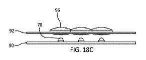
図18Aは、バッフルプレート92のバッフル94中にそれぞれ挿入された円形レンズ96の斜視図である。円形レンズ96の各々は、対応のバッフル94からの第1の放射線ビームを受け入れて第1の放射線ビームよりも集束度の高い第2の放射線ビームを投射するよう構成されている。図18Bは、バッフルプレート92のバッフル94中に挿入された円形レンズ96の平面図である。円形レンズの周長は、バッフルの周長よりも大きいのが良く、その結果、円形レンズのリムは、バッフルプレート92の頂面上に載ることができる。図18Cは、バッフルプレート92のバッフル94中に挿入された円形レンズ96の側面図である。図18Cに示されているように、円形レンズ96の底部分は、バッフル94から突き出るのが良い。一実施形態では、円形レンズ96は、プラスチックで作られた平凸レンズであるのが良い。別の実施形態では、円形レンズ96は、両凸レンズであるのが良い。
FIG. 18A is a perspective view of the
図19Aは、円形レンズ96上に設けられた六角形レンズ98の斜視図である。六角形レンズ98の各々は、対応の円形レンズ96からの第2の放射線ビームを受け入れ、そして第3のビーム(これは実質的に平行にされている)を焦点面120の方へ投射するよう構成されている。六角形レンズ98の各々は、凸状頂面98Aおよび6つの平坦な側壁98Bを有するのが良い。特に、頂面98Aは、非球面であるのが良い。種々の実施形態では、素子50は、六角形セル相互間に(すなわち仕切り、ダイヤフラム)を形成する薄い材料シートであるのが良い。他の場合、素子50は、レンズ98の各々を包囲した覆いまたは被膜、クラッディングであるのが良い。特定の一実施例では、素子50は、レンズ98を互いに結合する光学的に不透明な(光硬化性液体ポリマーを硬化させる放射線の波長の状態にある)接着剤であるのが良い。
FIG. 19A is a perspective view of the
比較のため、不透明な接着剤50は、正方形セル実施形態の仕切り74の役割を果たすことが注目される。不透明接着剤50の厚さ(例えば、5ミクロン)は、仕切り壁74の厚さ(例えば、1mm)よりも実質的に小さいので、不透明接着剤50に起因するシャドー効果は、仕切り74のシャドー効果と比較して実質的に低い。その結果、六角形セル光源に必要な不透明接着剤50のシャドー効果についての補償が事実上なく、その結果、セルエッジのところの非一様性が小さくなる。図19Bおよび図19Cは、それぞれ、円形レンズ46上に設けられた六角形レンズ98の平面図および側面図である。六角形レンズ98の底面98Cが部分的に図19Cに見える。互いにくっつけられる六角形レンズ98のアンサンブルまたは組み合わせの周囲を支持するために構造体(図示せず)が用いられる。
For comparison, it is noted that the opaque adhesive 50 acts as a
図20は、本発明の一実施形態に従って光エンジン1つの六角形セルと関連したある特定のコンポーネントの斜視図である。図20には、頂面98A、6つの側面98B、および底面98Cを備えた六角形レンズ98が記載されている。円形レンズ96が六角形レンズ98とLED70との間に設けられている。図20にはバッフルが図示されていない。多数のかかるレンズが光エンジン全体内に存在するのが良い。さらに、上記説明では1つのLEDが各セルについて存在しているが、別の実施形態では、多数のLED(例えば、1つまたは2つ以上のUV、1つの赤色、1つの緑色、および/または1つの青色LED)が各セル内に存在していても良い。
FIG. 20 is a perspective view of a particular component associated with one hexagonal cell of an optical engine according to an embodiment of the invention. FIG. 20 shows a
上述の実施形態に加えて、本発明の別の実施形態は、レンズアレイをなした正方形または他のレンズに代えて、テレセントリックレンズを採用することができる。テレセントリックレンズは、複合レンズであり、本発明の実施形態は、無限遠のところに入射瞳と出射瞳の両方を有するものとして特徴づけられるバイテレセントリックレンズを採用するのが良い。バイテレセントリックレンズの使用により、平行光源からの照明の際の像ディストーション(例えば、糸巻き型歪曲および/または樽型歪曲)および他の誤差を減少させることができる。 In addition to the embodiments described above, another embodiment of the invention may employ a telecentric lens in place of a square or other lens with a lens array. The telecentric lens is a composite lens, and embodiments of the present invention preferably employ a bi-telecentric lens characterized as having both entrance and exit pupils at infinity. The use of bi-telecentric lenses can reduce image distortion (eg, pincushion distortion and / or barrel distortion) and other errors when illuminated from parallel light sources.
変形例として、上述の正方形レンズまたは他のレンズに代えて、レンズアレイ中にフレネルレンズを採用しても良い。例えば、ヴ等(Vu et al.),「エルイーディー・ユニフォーム・イルミネーション・ユージング・ダブル・リニア・フレネル・レンズ・フォー・エネルギー・セービング(LED Uniform Illumination Using Double Linear Fresnel for Energy Saving)」,エナジーズ(Energies)2017年,10,2091(2017年12月11日)は、LEDのアレイのためのかかるコリメータの使用を記載している。本発明の実施形態では、直線フレネルレンズアレイは、所望の焦点距離が得られるよう比較的薄いという利点を提供する。LED源からできるだけ多くの光を捕捉するため、追加のプリズム素子を用いてLEDによって放出された光を個々のレンズ素子に方向づけるのが良い。代替的にまたは追加的に、個々のLEDは、もしそのように構成されていなければバッフルによって吸収される追加の光の方向をアレイのレンズに向け直すようレフレクタによって包囲されても良い。 As a modification, a Fresnel lens may be adopted in the lens array instead of the above-mentioned square lens or other lens. For example, Vu et al., "LED Uniform Illumination Using Double Linear Fresnel for Energy Saving", Energy Savings (LED Uniform Illumination Using Double Linear Fresnel for Energy Saving). Energies) 2017, 10, 2091 (December 11, 2017) describes the use of such a collimator for an array of LEDs. In embodiments of the invention, the linear Fresnel lens array offers the advantage of being relatively thin to obtain the desired focal length. In order to capture as much light as possible from the LED source, it is advisable to use additional prism elements to direct the light emitted by the LEDs to the individual lens elements. Alternatively or additionally, the individual LEDs may be surrounded by a reflector to direct the direction of the additional light absorbed by the baffle, if not so configured, towards the lenses of the array.
上述の実施形態では、LEDおよび平行光学系の直線配置状態を説明したが、他の配置状態の採用が可能である。例えば、LEDがタンク中への最終的な光投射平面に対して直交方向に光を放出するよう配置されている側照明配置状態を用いることができる。かかる「側照明」または「縁照明」配置状態は、光をLCDユニットに方向づけるようコリメートフィルム、例えばミネソタ州セントポール所在のスリーエム・カンパニー(3M Company)製のいわゆるブライトネス・エンハンスメント・フィルムズ(Brightness Enhancement Films)を採用するのが良い。これらフィルムは、入射光の方向を変えるようプリズム構造を採用している。 In the above-described embodiment, the linear arrangement state of the LED and the parallel optical system has been described, but other arrangement states can be adopted. For example, a side illumination arrangement state in which the LEDs are arranged to emit light in a direction orthogonal to the final light projection plane into the tank can be used. Such "side lighting" or "edge lighting" placement conditions are collimated films that direct light to the LCD unit, such as the so-called Brightness Enhancement Films from 3M Company in St. Paul, Minnesota . ) Is better to adopt. These films employ a prism structure to change the direction of incident light.
さらに、光源としてのLEDの使用を上述の実施形態と関連して説明したが、他の光源を採用することができる。例えば、水銀アーク灯が伝統的にフォトリソグラフィ用途において紫外線の源として用いられており、かかる水銀アーク灯を同様に、本明細書において説明したように光エンジンに採用することができる。 Further, although the use of LEDs as light sources has been described in connection with the above embodiments, other light sources can be employed. For example, mercury arc lamps have traditionally been used as sources of ultraviolet light in photolithography applications, and such mercury arc lamps can also be employed in optical engines as described herein.
かくして、立体物の形成のために液体ポリマーの光硬化を利用する3Dプリンティング装置で用いられる光エンジンについて説明した。
なお、好ましい構成態様として、本発明を次のように構成することもできる。
1. 放射線への暴露によって光硬化性液体ポリマーを光硬化させることによって立体物を形成する装置であって、前記液体ポリマーを収容したタンクと、前記放射線を放出する平行光源とを有し、前記光硬化性液体ポリマーは、前記タンクに設けられている開口部を通って硬化される、立体物の形成装置。
2. 前記平行光源は、発光ダイオード(LED)源のアレイから成り、前記LED源のうちの少なくとも幾つかは、放射線を400~700nmの波長で放出するよう構成されている、上記1記載の立体物の形成装置。
3. 前記平行光源は、発光ダイオード(LED)源のアレイから成り、前記LED源のうちの少なくとも幾つかは、放射線を410nmの波長で放出するよう構成されている、上記2記載の立体物の形成装置。
4. 前記平行光源は、バッフルのアレイおよびレンズのアレイをさらに有し、前記バッフルは、前記LED源のアレイ中の個々のLED源の各々のビーム幅を前記レンズのアレイに属する一レンズのほぼ直径に制限するよう配置され、前記レンズのアレイは、前記LED源のアレイから焦点距離1つ分のところに配置されている、上記3記載の立体物の形成装置。
5. 前記LED源のうちの1つまたは2つ以上は、放射線を複数の波長で放出するよう構成されている、上記2記載の立体物の形成装置。
6. 前記平行光源は、バッフルのアレイおよびレンズのアレイをさらに有し、前記バッフルは、前記LED源のアレイ中の個々のLED源の各々のビーム幅を前記レンズのアレイに属する一レンズのほぼ直径に制限するよう配置され、前記レンズのアレイは、前記LED源のアレイから焦点距離1つ分のところに配置されている、上記2記載の立体物の形成装置。
7. 前記平行光源は、液晶ディスプレイ(“LCD”)をさらに有し、前記LCDは、前記LEDのアレイと前記タンク内に設けられた一領域との間に位置決めされ、物体が前記一領域内において前記光硬化性液体ポリマーの光硬化によって作製される、上記2記載の立体物の形成装置。
8. 前記LCDは、複数のフィルタを含み、前記複数のフィルタの各フィルタは、放出された放射線の前記波長のうちの1つに対応している、上記7記載の立体物の形成装置。
9. 前記LED源のうちの1つまたは2つ以上は、複数のLEDエミッタから成り、前記エミッタの各々は、放射線を1つまたは2つ以上の波長で放出するよう構成されている、上記2記載の立体物の形成装置。
10. 前記平行光源は、
複数の発光ダイオード(LED)群を有し、前記LED群の各々に対応して、
(i)前記LED群から伝搬している電磁線の第1のビームを拘束するとともに方向づけるよう構成されたバッフルと、
(ii)前記電磁線の第1のビームを受け入れて電磁線の第2のビームを投射するよう構成されたレンズ配列体とを有し、前記電磁線の第2のビームは、実質的に互いに平行な光線によって特徴づけられる、上記1記載の立体物の形成装置。
11. 前記複数のLED群の各々は、2つ以上のLEDを含む、上記10記載の立体物の形成装置。
12. 放射線に暴露された光硬化性液体ポリマーを光硬化させることによって立体物を形成する方法であって、前記立体物は、前記放射線に対して透明なシートと支持プレート、すなわち前記立体物のすでに形成された一部分との間の空間内で、前記光硬化性液体ポリマーの漸次硬化に起因して成長により生じ、前記支持プレートは、前記透明なシートから徐々に遠ざかる、方法において、前記光硬化性液体ポリマーを平行光源からの照射によって硬化させる、立体物の形成方法。
13. 前記平行光源は、発光ダイオード(LED)源のアレイから成る、上記12記載の立体物の形成方法。
14. 前記LED源は、放射線を400~700nmの波長で放出する、上記13記載の立体物の形成方法。
15. 前記平行光源は、バッフルのアレイおよびレンズのアレイを含み、前記バッフルは、前記LED源のアレイ中の個々のLED源の各々のビーム幅を前記レンズのアレイに属する一レンズのほぼ直径に制限するよう配置され、前記レンズのアレイは、前記LED源のアレイから焦点距離1つ分のところに配置されている、上記13記載の立体物の形成方法。
Thus, an optical engine used in a 3D printing device that utilizes photocuring of a liquid polymer for the formation of a three-dimensional object has been described.
In addition, as a preferable configuration mode, the present invention can also be configured as follows.
1. 1. A device for forming a three-dimensional object by photocuring a photocurable liquid polymer by exposure to radiation, having a tank containing the liquid polymer and a parallel light source emitting the radiation, and the photocuring. The sex liquid polymer is a three-dimensional object forming device that is cured through an opening provided in the tank.
2. 2. The three-dimensional object according to 1 above, wherein the parallel light source comprises an array of light emitting diode (LED) sources, and at least some of the LED sources are configured to emit radiation at a wavelength of 400 to 700 nm. Forming device.
3. 3. The three-dimensional object forming apparatus according to the above 2, wherein the parallel light source comprises an array of light emitting diode (LED) sources, and at least some of the LED sources are configured to emit radiation at a wavelength of 410 nm. ..
4. The parallel light source further comprises an array of baffles and an array of lenses, which baffles bring the beam width of each of the individual LED sources in the array of LED sources to approximately the diameter of one lens belonging to the array of lenses. 3. The stereoscopic object forming apparatus according to 3 above, wherein the lens array is arranged so as to be restricted, and the lens array is arranged at a focal length of one from the LED source array.
5. The three-dimensional object forming apparatus according to the above 2, wherein one or more of the LED sources are configured to emit radiation at a plurality of wavelengths.
6. The parallel light source further comprises an array of baffles and an array of lenses, which baffles bring the beam width of each of the individual LED sources in the array of LED sources to approximately the diameter of one lens belonging to the array of lenses. 2. The three-dimensional object forming apparatus according to the above 2, wherein the lens array is arranged so as to be restricted, and the lens array is arranged at a focal length of one from the LED source array.
7. The parallel light source further comprises a liquid crystal display (“LCD”), the LCD being positioned between the array of LEDs and an area provided within the tank, the object being said within the area. The apparatus for forming a three-dimensional object according to the above 2, which is produced by photocuring a photocurable liquid polymer.
8. 7. The three-dimensional object forming apparatus according to 7 above, wherein the LCD includes a plurality of filters, and each filter of the plurality of filters corresponds to one of the wavelengths of the emitted radiation.
9. 2. The above two, wherein one or more of the LED sources consist of a plurality of LED emitters, each of which is configured to emit radiation at one or more wavelengths. A device for forming a three-dimensional object.
10. The parallel light source is
It has a plurality of light emitting diode (LED) groups, and corresponds to each of the LED groups.
(I) A baffle configured to constrain and direct the first beam of electromagnetic rays propagating from the LED group.
(Ii) It has a lens array configured to receive the first beam of the electromagnetic rays and project the second beam of the electromagnetic rays, and the second beams of the electromagnetic rays are substantially mutually exclusive. The three-dimensional object forming apparatus according to 1 above, which is characterized by parallel light rays.
11. 10. The three-dimensional object forming apparatus according to 10 above, wherein each of the plurality of LED groups includes two or more LEDs.
12. A method of forming a three-dimensional object by photo-curing a photocurable liquid polymer exposed to radiation, wherein the three-dimensional object already forms a sheet and a support plate transparent to the radiation, that is, the three-dimensional object. In the space between the photocurable liquid polymer, the support plate is formed by growth due to the gradual curing of the photocurable liquid polymer, and the support plate is gradually moved away from the transparent sheet. A method for forming a three-dimensional object, in which a polymer is cured by irradiation from a parallel light source.
13. 12. The method for forming a three-dimensional object according to the above 12, wherein the parallel light source comprises an array of light emitting diode (LED) sources.
14. 13. The method for forming a three-dimensional object according to the above 13, wherein the LED source emits radiation at a wavelength of 400 to 700 nm.
15. The parallel light source includes an array of baffles and an array of lenses, which limits the beam width of each of the individual LED sources in the array of LED sources to approximately the diameter of one lens belonging to the array of lenses. 13. The method for forming a three-dimensional object according to the above 13, wherein the lens array is arranged at a focal length of one from the LED source array.
Claims (11)
Applications Claiming Priority (11)
| Application Number | Priority Date | Filing Date | Title |
|---|---|---|---|
| US201762450470P | 2017-01-25 | 2017-01-25 | |
| US62/450,470 | 2017-01-25 | ||
| US15/415,688 | 2017-01-25 | ||
| US15/415,688 US11260579B2 (en) | 2015-10-02 | 2017-01-25 | Methods for photo-curing with displaceable self-lubricating substratum for the formation of three-dimensional objects |
| US201762531211P | 2017-07-11 | 2017-07-11 | |
| US201762531276P | 2017-07-11 | 2017-07-11 | |
| US62/531,276 | 2017-07-11 | ||
| US62/531,211 | 2017-07-11 | ||
| US201762531461P | 2017-07-12 | 2017-07-12 | |
| US62/531,461 | 2017-07-12 | ||
| PCT/US2018/012774 WO2018140218A1 (en) | 2017-01-25 | 2018-01-08 | Method and apparatus using light engines for photo-curing of liquid polymers to form three-dimensional objects |
Publications (2)
| Publication Number | Publication Date |
|---|---|
| JP2020504041A JP2020504041A (en) | 2020-02-06 |
| JP7055424B2 true JP7055424B2 (en) | 2022-04-18 |
Family
ID=62978716
Family Applications (1)
| Application Number | Title | Priority Date | Filing Date |
|---|---|---|---|
| JP2019539903A Active JP7055424B2 (en) | 2017-01-25 | 2018-01-08 | Methods and equipment using an optical engine for photocuring of liquid polymers to form three-dimensional objects |
Country Status (9)
| Country | Link |
|---|---|
| EP (1) | EP3573813A1 (en) |
| JP (1) | JP7055424B2 (en) |
| KR (1) | KR102442533B1 (en) |
| CN (1) | CN110225813A (en) |
| AU (1) | AU2018213856B2 (en) |
| CA (1) | CA3048515A1 (en) |
| IL (1) | IL267976B (en) |
| TW (1) | TWI765954B (en) |
| WO (1) | WO2018140218A1 (en) |
Families Citing this family (11)
| Publication number | Priority date | Publication date | Assignee | Title |
|---|---|---|---|---|
| US11858215B2 (en) * | 2018-04-30 | 2024-01-02 | Hewlett-Packard Development Company, L.P. | Build material heaters with baffles |
| CN109633946B (en) * | 2019-01-31 | 2022-05-24 | 上海天马微电子有限公司 | Display device, manufacturing method thereof and 3D printing system |
| GB2584493A (en) * | 2019-06-07 | 2020-12-09 | Xaar 3D Ltd | Radiation source assembly and apparatus for layer-by-layer formation of three-dimensional objects |
| WO2020253635A1 (en) * | 2019-06-17 | 2020-12-24 | Luxcreo (Beijing) Inc. | Systems and methods for three-dimensional printing |
| CN110524874B (en) * | 2019-08-23 | 2022-03-08 | 源秩科技(上海)有限公司 | Photocuring 3D printing device and printing method thereof |
| KR102367742B1 (en) * | 2019-12-10 | 2022-02-25 | (주)캐리마 | Light source Device of line shape and 3D Printer comprising the same |
| CN113290860A (en) * | 2021-07-14 | 2021-08-24 | 深圳市鹏基光电有限公司 | Photocuring 3D printer light machine, printer and light emitting display method |
| CN216782664U (en) * | 2021-10-14 | 2022-06-21 | 深圳市纵维立方科技有限公司 | Light source device and photocuring printer |
| CN114506079A (en) * | 2022-02-25 | 2022-05-17 | 深圳市纵维立方科技有限公司 | Light source subassembly and 3D printer |
| WO2023190399A1 (en) * | 2022-03-28 | 2023-10-05 | 三井化学株式会社 | Optical shaping device, reduced projection optical component for optical shaping device, and method for manufacturing optically shaped article |
| US20240051227A1 (en) * | 2022-08-11 | 2024-02-15 | NEXA3D Inc. | Light engines for vat polimerization 3d printers |
Citations (5)
| Publication number | Priority date | Publication date | Assignee | Title |
|---|---|---|---|---|
| JP2002370286A (en) | 2001-04-23 | 2002-12-24 | Envision Technologies Gmbh | Apparatus and method for separating material layer |
| JP2010253882A (en) | 2009-04-28 | 2010-11-11 | Konica Minolta Opto Inc | Image forming apparatus and lens array |
| JP2012519874A (en) | 2009-03-06 | 2012-08-30 | ネーデルランデ オルガニサチエ ヴォール トエゲパスト−ナツールウェテンスハペリエク オンデルゾエク ティーエヌオー | Irradiation system for stereolithography equipment |
| US20150290876A1 (en) | 2014-04-09 | 2015-10-15 | Yanjun Liu | Stereolithographic apparatus and method |
| JP2016540665A (en) | 2013-11-14 | 2016-12-28 | ストラクト ピーティーイー.エルティーディーStructo Pte. Ltd | Additive manufacturing apparatus and method |
Family Cites Families (10)
| Publication number | Priority date | Publication date | Assignee | Title |
|---|---|---|---|---|
| TW269010B (en) * | 1994-04-04 | 1996-01-21 | Projectavision Inc | |
| JP3608333B2 (en) * | 1997-03-06 | 2005-01-12 | ソニー株式会社 | Optical pickup and method of assembling objective lens for optical pickup |
| EP2218571A1 (en) * | 2009-01-30 | 2010-08-18 | Nederlandse Organisatie voor toegepast -natuurwetenschappelijk onderzoek TNO | Illumination system for use in a stereolithography apparatus |
| CN103119513A (en) * | 2010-09-22 | 2013-05-22 | 3M创新有限公司 | Tilted dichroic color combiner II |
| EP2771734B1 (en) * | 2011-10-24 | 2017-07-19 | 3M Innovative Properties Company | Tilted dichroic polarizing beamsplitter |
| US8663539B1 (en) * | 2012-04-02 | 2014-03-04 | Hrl Laboratories, Llc | Process of making a three-dimentional micro-truss structure |
| JP6600315B2 (en) * | 2013-12-03 | 2019-10-30 | プリズムラボ チャイナ リミテッド | Photo-curable 3D printing apparatus and imaging system therefor |
| CN104669619B (en) * | 2013-12-03 | 2019-03-05 | 上海普利生机电科技有限公司 | Light-cured type 3D printing equipment and its imaging system |
| CN203766034U (en) * | 2014-04-09 | 2014-08-13 | 刘彦君 | Light source device used for 3D printer and 3D printer |
| KR101667522B1 (en) * | 2015-03-10 | 2016-10-19 | 에스팩 주식회사 | 3d printing method using liquid crystal matrix as mask, and 3d printing device |
-
2018
- 2018-01-08 AU AU2018213856A patent/AU2018213856B2/en active Active
- 2018-01-08 CA CA3048515A patent/CA3048515A1/en active Pending
- 2018-01-08 CN CN201880008420.0A patent/CN110225813A/en active Pending
- 2018-01-08 KR KR1020197020728A patent/KR102442533B1/en active IP Right Grant
- 2018-01-08 WO PCT/US2018/012774 patent/WO2018140218A1/en unknown
- 2018-01-08 JP JP2019539903A patent/JP7055424B2/en active Active
- 2018-01-08 EP EP18703385.7A patent/EP3573813A1/en active Pending
- 2018-01-08 IL IL267976A patent/IL267976B/en unknown
- 2018-01-16 TW TW107101519A patent/TWI765954B/en active
Patent Citations (5)
| Publication number | Priority date | Publication date | Assignee | Title |
|---|---|---|---|---|
| JP2002370286A (en) | 2001-04-23 | 2002-12-24 | Envision Technologies Gmbh | Apparatus and method for separating material layer |
| JP2012519874A (en) | 2009-03-06 | 2012-08-30 | ネーデルランデ オルガニサチエ ヴォール トエゲパスト−ナツールウェテンスハペリエク オンデルゾエク ティーエヌオー | Irradiation system for stereolithography equipment |
| JP2010253882A (en) | 2009-04-28 | 2010-11-11 | Konica Minolta Opto Inc | Image forming apparatus and lens array |
| JP2016540665A (en) | 2013-11-14 | 2016-12-28 | ストラクト ピーティーイー.エルティーディーStructo Pte. Ltd | Additive manufacturing apparatus and method |
| US20150290876A1 (en) | 2014-04-09 | 2015-10-15 | Yanjun Liu | Stereolithographic apparatus and method |
Also Published As
| Publication number | Publication date |
|---|---|
| JP2020504041A (en) | 2020-02-06 |
| KR102442533B1 (en) | 2022-09-13 |
| KR20190103210A (en) | 2019-09-04 |
| AU2018213856A1 (en) | 2019-07-04 |
| CN110225813A (en) | 2019-09-10 |
| IL267976B (en) | 2022-08-01 |
| EP3573813A1 (en) | 2019-12-04 |
| CA3048515A1 (en) | 2018-08-02 |
| WO2018140218A4 (en) | 2018-08-30 |
| TWI765954B (en) | 2022-06-01 |
| IL267976A (en) | 2019-09-26 |
| AU2018213856B2 (en) | 2022-12-22 |
| TW201834869A (en) | 2018-10-01 |
| WO2018140218A1 (en) | 2018-08-02 |
Similar Documents
| Publication | Publication Date | Title |
|---|---|---|
| JP7055424B2 (en) | Methods and equipment using an optical engine for photocuring of liquid polymers to form three-dimensional objects | |
| US10328634B2 (en) | Light engines for photo-curing of liquid polymers to form three-dimensional objects | |
| JP6966807B2 (en) | Addition manufacturing equipment and methods | |
| US10399270B2 (en) | Photo-curing 3D printer and 3D printing method | |
| KR101117912B1 (en) | Multilayered screens with light-emitting stripes for scanning beam display systems | |
| JP6600315B2 (en) | Photo-curable 3D printing apparatus and imaging system therefor | |
| JP2008155650A (en) | Apparatus for manufacturing three-dimensional object | |
| CN109143663A (en) | A kind of liquid crystal display panel and 3D printer | |
| CN104669622A (en) | Photocurable 3D (three-dimensional) printing device and imaging system thereof | |
| US20240051227A1 (en) | Light engines for vat polimerization 3d printers | |
| RU220761U1 (en) | Multiple exposure photopolymer 3D printer | |
| JP3391242B2 (en) | Transmission screen | |
| KR101136055B1 (en) | Ultra violet curing apparatus and method using digital micro-mirror device | |
| EP4173805A1 (en) | An imaging module for a uv lcd 3d printer | |
| JP2009251559A (en) | Optical element, preparation method of optical element and projection type display apparatus | |
| JPH06148407A (en) | Fresnel lens sheet | |
| KR20060112565A (en) | Manufacturing method of lenticular screen and display apparatus menufactured thereby |
Legal Events
| Date | Code | Title | Description |
|---|---|---|---|
| A521 | Request for written amendment filed |
Free format text: JAPANESE INTERMEDIATE CODE: A523 Effective date: 20190731 |
|
| A621 | Written request for application examination |
Free format text: JAPANESE INTERMEDIATE CODE: A621 Effective date: 20201216 |
|
| A977 | Report on retrieval |
Free format text: JAPANESE INTERMEDIATE CODE: A971007 Effective date: 20211115 |
|
| A131 | Notification of reasons for refusal |
Free format text: JAPANESE INTERMEDIATE CODE: A131 Effective date: 20211124 |
|
| A521 | Request for written amendment filed |
Free format text: JAPANESE INTERMEDIATE CODE: A523 Effective date: 20220222 |
|
| TRDD | Decision of grant or rejection written | ||
| A01 | Written decision to grant a patent or to grant a registration (utility model) |
Free format text: JAPANESE INTERMEDIATE CODE: A01 Effective date: 20220307 |
|
| A61 | First payment of annual fees (during grant procedure) |
Free format text: JAPANESE INTERMEDIATE CODE: A61 Effective date: 20220330 |
|
| R150 | Certificate of patent or registration of utility model |
Ref document number: 7055424 Country of ref document: JP Free format text: JAPANESE INTERMEDIATE CODE: R150 |