以下、図面を参照しながら、本開示の発光装置の実施形態を詳細に説明する。以下の実施形態は、例示であり、本開示の発光装置は、以下の実施形態に限られない。以下の説明では、特定の方向または位置を示す用語(例えば、「上」、「下」、「右」、「左」およびそれらの用語を含む別の用語)を用いる場合がある。それらの用語は、参照した図面における相対的な方向または位置を分かり易く示すために用いているに過ぎない。参照した図面における「上」、「下」等の用語による相対的な方向または位置の関係が同一であれば、本開示以外の図面、実際の製品等において、参照した図面と同一の配置でなくてもよい。また、図面が示す構成要素の大きさおよび位置関係等は、分かり易さのため、誇張されている場合があり、実際の発光装置における大きさ、あるいは、実際の発光装置における構成要素間の大小関係を厳密に反映していない場合がある。なお、図面が過度に複雑となることを避けるため、模式的な断面図等において一部の要素の図示を省略することがある。
Hereinafter, embodiments of the light emitting device of the present disclosure will be described in detail with reference to the drawings. The following embodiments are examples, and the light emitting device of the present disclosure is not limited to the following embodiments. In the following description, terms indicating a specific direction or position (eg, "top", "bottom", "right", "left" and other terms including those terms) may be used. These terms are only used to clearly indicate the relative orientation or position in the referenced drawing. If the relative directions or positional relationships in terms such as "top" and "bottom" in the referenced drawings are the same, the layout is not the same as the referenced drawings in drawings other than the present disclosure, actual products, etc. You may. In addition, the size and positional relationship of the components shown in the drawings may be exaggerated for the sake of clarity, and may be the size in the actual light emitting device or the size between the components in the actual light emitting device. It may not exactly reflect the relationship. In addition, in order to avoid the drawing from becoming excessively complicated, the illustration of some elements may be omitted in a schematic cross-sectional view or the like.
(第1の実施形態)
図1は、本開示の第1の実施形態による発光装置の断面を模式的に示す。参考のために、図1には、互いに直交するx方向、y方向およびz方向を示す矢印が描かれている。本開示の他の図面においてもこれらの矢印を示すことがある。図1に示す発光装置100Aは、基板10と、複数の光源20と、波長変換層30Aと、散乱反射部50と、光拡散板70とを有する。発光装置100Aは、例えば、液晶表示装置等のバックライトとして利用される。以下、各構成要素を詳細に説明する。
(First Embodiment)
FIG. 1 schematically shows a cross section of a light emitting device according to the first embodiment of the present disclosure. For reference, in FIG. 1, arrows indicating the x-direction, y-direction, and z-direction orthogonal to each other are drawn. Other drawings of the present disclosure may also indicate these arrows. The light emitting device 100A shown in FIG. 1 includes a substrate 10, a plurality of light sources 20, a wavelength conversion layer 30A, a scattering / reflecting unit 50, and a light diffusing plate 70. The light emitting device 100A is used, for example, as a backlight for a liquid crystal display device or the like. Hereinafter, each component will be described in detail.
[基板10]
基板10は、上面10aおよび下面10bを有する。複数の光源20は、基板10の上面10a上に位置する。
[Board 10]
The substrate 10 has an upper surface 10a and a lower surface 10b. The plurality of light sources 20 are located on the upper surface 10a of the substrate 10.
基板10の材料としては、例えば、セラミックスおよび樹脂を用いることができる。低コストおよび成形容易性の点から、樹脂を基板10の材料として選択してもよい。樹脂としては、フェノール樹脂、エポキシ樹脂、ポリイミド樹脂、ビスマレイミドトリアジン樹脂(BTレジン)、ポリフタルアミド(PPA)、ポリエチレンテレフタレート(PET)、ポリエチレンナフタレート(PEN)等を挙げることができる。基板10は、リジット基板であってもよいし、ロール・ツー・ロール方式で製造可能なフレキシブル基板であってもよい。基板10の厚さは、適宜選択することができる。リジット基板は、湾曲可能な薄型リジット基板であってもよい。
As the material of the substrate 10, for example, ceramics and resin can be used. Resin may be selected as the material of the substrate 10 from the viewpoint of low cost and ease of molding. Examples of the resin include phenol resin, epoxy resin, polyimide resin, bismaleimide triazine resin (BT resin), polyphthalamide (PPA), polyethylene terephthalate (PET), polyethylene naphthalate (PEN) and the like. The substrate 10 may be a rigid substrate or a flexible substrate that can be manufactured by a roll-to-roll method. The thickness of the substrate 10 can be appropriately selected. The rigid substrate may be a bendable thin rigid substrate.
また、耐熱性および耐光性に優れるという観点から、セラミックスを基板10の材料として選択してもよい。セラミックスとしては、例えば、アルミナ、ムライト、フォルステライト、ガラスセラミックス、窒化物系(例えば、AlN)、炭化物系(例えば、SiC)、LTCC(Low Temperature Co-fired Ceramics)等が挙げられる。
Further, ceramics may be selected as the material of the substrate 10 from the viewpoint of excellent heat resistance and light resistance. Examples of the ceramics include alumina, mulite, forsterite, glass ceramics, nitride-based (for example, AlN), carbide-based (for example, SiC), and LTCC (Low Temperature Co-fired Ceramics).
基板10は、複合材料によって形成されていてもよく、例えば、上述した樹脂に、ガラス繊維、SiO2、TiO2、Al2O3等の無機フィラーを混合してもよい。これにより、基板10の機械的強度の向上、熱膨張率の低減、光反射率の向上等を図ることができる。例えば、ガラス繊維強化樹脂(ガラスエポキシ樹脂)等を基板10の材料として用いてもよい。
The substrate 10 may be formed of a composite material, and for example, the above-mentioned resin may be mixed with an inorganic filler such as glass fiber, SiO 2 , TiO 2 , or Al 2 O 3 . As a result, it is possible to improve the mechanical strength of the substrate 10, reduce the coefficient of thermal expansion, improve the light reflectance, and the like. For example, a glass fiber reinforced resin (glass epoxy resin) or the like may be used as the material of the substrate 10.
基板10は、その上面10aに、光源20への給電のための導体配線層を有する配線基板であり得る。基板10は、少なくとも上面10aが電気的絶縁性を有していればよく、例えば、基板10として、表面に絶縁層が設けられた金属板を用いることも可能である。基板10は、積層構造を有していてもよい。
The substrate 10 may be a wiring board having a conductor wiring layer for supplying power to the light source 20 on its upper surface 10a. The substrate 10 may have at least the upper surface 10a having an electrical insulating property, and for example, a metal plate having an insulating layer on the surface thereof can be used as the substrate 10. The substrate 10 may have a laminated structure.
[導体配線層12]
図2は、図1の一部を拡大して模式的に示す。図2に例示する構成において、発光装置100Aは、基板10の上面10aに設けられた導体配線層12を有する。導体配線層12は、各光源20に外部から電力を供給する配線パターンを有する。ここでは、各光源20は、後述する接合部材26によって正極および負極が導体配線層12に接続されることにより、導体配線層12に電気的に接続され、かつ、固定されている。
[Conductor wiring layer 12]
FIG. 2 schematically shows a part of FIG. 1 in an enlarged manner. In the configuration exemplified in FIG. 2, the light emitting device 100A has a conductor wiring layer 12 provided on the upper surface 10a of the substrate 10. The conductor wiring layer 12 has a wiring pattern for supplying electric power to each light source 20 from the outside. Here, each light source 20 is electrically connected to and fixed to the conductor wiring layer 12 by connecting the positive electrode and the negative electrode to the conductor wiring layer 12 by a joining member 26 described later.
導体配線層12の材料は、基板10の材料および製造方法等に応じて適宜選択することができる。基板10の材料として例えばセラミックスを用いる場合には、導体配線層12の材料として、基板10のセラミックスと同時焼成が可能な高融点金属を用い得る。例えば、タングステン、モリブデン等の高融点金属によって導体配線層12を形成することができる。基板10の材料として例えばガラスエポキシ樹脂を用いる場合であれば、導体配線層12の材料として、加工し易い材料を選択すると有益である。例えば、メッキ、スパッタリング、蒸着、プレスによる貼り付けによって形成された、銅、ニッケル等の金属層を導体配線層12として用いることができる。導体配線層12の形成方法として、印刷、フォトリソグラフィー等を適用すれば、所定の配線パターンを有する金属層を比較的容易に形成可能である。
The material of the conductor wiring layer 12 can be appropriately selected depending on the material of the substrate 10, the manufacturing method, and the like. When, for example, ceramics are used as the material of the substrate 10, a refractory metal capable of simultaneous firing with the ceramics of the substrate 10 can be used as the material of the conductor wiring layer 12. For example, the conductor wiring layer 12 can be formed of a refractory metal such as tungsten or molybdenum. When, for example, a glass epoxy resin is used as the material of the substrate 10, it is beneficial to select a material that is easy to process as the material of the conductor wiring layer 12. For example, a metal layer such as copper or nickel formed by plating, sputtering, vapor deposition, or pasting by pressing can be used as the conductor wiring layer 12. If printing, photolithography, or the like is applied as a method for forming the conductor wiring layer 12, a metal layer having a predetermined wiring pattern can be relatively easily formed.
導体配線層12は、複数の配線パターンを含み得る。各配線パターンは、光源20を駆動するドライバに接続され得る。例えば、各配線パターンは、複数の光源20のうちの1つとドライバとを電気的に接続する。各配線パターンのそれぞれが、2以上の光源20を直列に接続してもよい。ドライバは、基板10とは別個の基板上に配置されて導体配線層12に電気的に接続されてもよいし、基板10上に配置されて導体配線層12に電気的に接続されてもよい。2以上の光源20を直列に接続する配線パターンを含む導体配線層12にドライバを接続することにより、複数の光源20を1個単位で、または、複数個の光源20が含まれるセグメントの単位で駆動させ、発光装置100Aをローカルディミング動作させることができる。
The conductor wiring layer 12 may include a plurality of wiring patterns. Each wiring pattern may be connected to a driver driving the light source 20. For example, each wiring pattern electrically connects one of the plurality of light sources 20 to the driver. Each of the wiring patterns may connect two or more light sources 20 in series. The driver may be arranged on a substrate separate from the substrate 10 and electrically connected to the conductor wiring layer 12, or may be arranged on the substrate 10 and electrically connected to the conductor wiring layer 12. .. By connecting a driver to the conductor wiring layer 12 including a wiring pattern in which two or more light sources 20 are connected in series, a plurality of light sources 20 are connected in units of one, or in units of segments including a plurality of light sources 20. It can be driven and the light source 100A can be operated by local dimming.
図3は、導体配線層12中の配線パターンの一例を示す。図3に例示する構成において、導体配線層12は、それぞれがn*m個の光源20に接続された複数の配線パターン12pを有している(「*」は、乗算を表す。)。各配線パターン12pは、n個の光源20を直列に接続し、かつ、直列に接続された光源20のm個の群を並列に接続している。これらの配線パターン12pは、ドライバ29に接続され、n*m個の光源20を含む領域DMを単位として駆動される。すなわち、このような回路構成のもとでは、n*m個の光源20を含む領域DMを単位とするローカルディミング動作が可能である。
FIG. 3 shows an example of a wiring pattern in the conductor wiring layer 12. In the configuration exemplified in FIG. 3, each of the conductor wiring layers 12 has a plurality of wiring patterns 12p connected to n * m light sources 20 (“*” represents multiplication). In each wiring pattern 12p, n light sources 20 are connected in series, and m groups of light sources 20 connected in series are connected in parallel. These wiring patterns 12p are connected to the driver 29 and are driven in units of region DM including n * m light sources 20. That is, under such a circuit configuration, local dimming operation in units of region DM including n * m light sources 20 is possible.
導体配線層12の配線の形態は、特定の形態に限定されない。ドライバによる導体配線層12を介した光源20の駆動方式は、パッシブマトリクス方式であってもよいし、アクティブマトリクス方式であってもよい。
The form of wiring of the conductor wiring layer 12 is not limited to a specific form. The driving method of the light source 20 via the conductor wiring layer 12 by the driver may be a passive matrix method or an active matrix method.
導体配線層12は、多層構造を有していてもよい。例えば導体配線層12は、上述した方法で形成された高融点金属のパターンと、このパターン上にメッキ、スパッタリング、蒸着等によって形成された、ニッケル、金、銀等の他の金属を含む層とを有していてもよい。
The conductor wiring layer 12 may have a multi-layer structure. For example, the conductor wiring layer 12 includes a pattern of a refractory metal formed by the above-mentioned method and a layer containing other metals such as nickel, gold, and silver formed on the pattern by plating, sputtering, vapor deposition, or the like. May have.
[金属層14]
図2に示すように、基板10の下面10bに金属層14を設けてもよい。金属層14は、例えば、下面10bの全体に設けられ、基板10の放熱性を向上させる。金属層14は、配線等を有していてもよく、例えば、光源20を駆動するための駆動回路の回路パター
ンを含み得る。駆動回路を構成する部品(例えば上述のドライバ)が金属層14の回路パターン上に実装されていてもよい。この場合、金属層14は、基板10内に設けられたビア導体等によって導体配線層12に電気的に接続される。
[Metal layer 14]
As shown in FIG. 2, a metal layer 14 may be provided on the lower surface 10b of the substrate 10. The metal layer 14 is provided on the entire lower surface 10b, for example, to improve the heat dissipation of the substrate 10. The metal layer 14 may have wiring or the like, and may include, for example, a circuit pattern of a drive circuit for driving the light source 20. The components constituting the drive circuit (for example, the driver described above) may be mounted on the circuit pattern of the metal layer 14. In this case, the metal layer 14 is electrically connected to the conductor wiring layer 12 by a via conductor or the like provided in the substrate 10.
[光源20]
複数の光源20は、基板10の上面10a側に配置および支持される。各光源20は、上面22aを有する発光素子22を少なくとも含む。発光素子22としては、半導体レーザ、発光ダイオード等、公知の半導体発光素子を利用することができる。本実施形態においては、発光素子22として発光ダイオードを例示する。
[Light source 20]
The plurality of light sources 20 are arranged and supported on the upper surface 10a side of the substrate 10. Each light source 20 includes at least a light emitting element 22 having an upper surface 22a. As the light emitting element 22, a known semiconductor light emitting element such as a semiconductor laser or a light emitting diode can be used. In this embodiment, a light emitting diode is exemplified as the light emitting element 22.
発光素子22は、例えば、透光性の基板と、基板の上に積層された半導体積層構造を有する。半導体積層構造は、活性層と、活性層を挟むn型半導体層およびp型半導体層とを含み、n型半導体層およびp型半導体層にn側電極およびp側電極がそれぞれ電気的に接続される。本実施形態では、n側電極およびp側電極は、上面22aと反対側の面に位置する。n側電極およびp側電極は、接合部材26によって、基板10の上面10aに設けられた導体配線層12に電気的に接続され、かつ、固定される。つまり、ここでは、光源20は、フリップチップボンディングにより基板10に実装されている。n側電極およびp側電極は、この例のように同一面側に配置されていてもよいし、それぞれが異なる面に配置されてもよい。発光素子22は、ベアチップであってもよいし、側面側にリフレクタを有するパッケージを備えていてもよい。また、発光素子22は、上面22aから出射する光の出射角度の範囲を広くするためのレンズ等を有していてもよい。
The light emitting element 22 has, for example, a translucent substrate and a semiconductor laminated structure laminated on the substrate. The semiconductor laminated structure includes an active layer, an n-type semiconductor layer and a p-type semiconductor layer sandwiching the active layer, and the n-side electrode and the p-side electrode are electrically connected to the n-type semiconductor layer and the p-type semiconductor layer, respectively. To. In the present embodiment, the n-side electrode and the p-side electrode are located on the surface opposite to the upper surface 22a. The n-side electrode and the p-side electrode are electrically connected to and fixed to the conductor wiring layer 12 provided on the upper surface 10a of the substrate 10 by the joining member 26. That is, here, the light source 20 is mounted on the substrate 10 by flip-chip bonding. The n-side electrode and the p-side electrode may be arranged on the same surface side as in this example, or may be arranged on different surfaces. The light emitting element 22 may be a bare chip or may be provided with a package having a reflector on the side surface side. Further, the light emitting element 22 may have a lens or the like for widening the range of the emission angle of the light emitted from the upper surface 22a.
図2において模式的に示すように、光源20は、発光素子22の上面22aに光反射層24を有していてもよい。図2に示す例のように発光素子22の上面22aの全体を覆う光反射層24を設けた場合、光は、発光素子22の側面から取り出される。発光素子22の上面22aに光反射層24を設けることにより、発光素子22の上方向(ここではz方向)への光が光反射層24で反射され、発光素子22の直上の光量が抑制される。結果としてバットウイング型の配光特性を実現し得る。このような構成によれば、バットウイング型の配光特性を付与するためのレンズ等を省略できるので、光源20の厚さを小さくすることに有利である。光反射層24は、例えば誘電体多層膜である。光反射層24は、金属膜であってもよい。
As schematically shown in FIG. 2, the light source 20 may have a light reflecting layer 24 on the upper surface 22a of the light emitting element 22. When the light reflecting layer 24 that covers the entire upper surface 22a of the light emitting element 22 is provided as in the example shown in FIG. 2, the light is taken out from the side surface of the light emitting element 22. By providing the light reflecting layer 24 on the upper surface 22a of the light emitting element 22, the light in the upward direction (here, the z direction) of the light emitting element 22 is reflected by the light reflecting layer 24, and the amount of light directly above the light emitting element 22 is suppressed. Ru. As a result, a bat wing type light distribution characteristic can be realized. According to such a configuration, it is possible to omit a lens or the like for imparting a butt wing type light distribution characteristic, which is advantageous in reducing the thickness of the light source 20. The light reflecting layer 24 is, for example, a dielectric multilayer film. The light reflecting layer 24 may be a metal film.
図4は、光源20から出射する光の配光特性の一例を示す。光源20は、バットウイング型の配光特性を有し得る。光源20がバットウイング型の配光特性を有すると、光源20の直上の光量を抑制して、各々の光源の配光を広げることができ、輝度むらを低減することができる。バットウイング型の配光特性とは、広義には、光源20の上面に垂直な光軸Lを0°として、0°よりも配光角(図2のφ)の絶対値が大きい角度において発光強度が高い発光強度分布で定義される。特に、狭義では、45°~90°付近において、発光強度が最も高くなる発光強度分布で定義される。つまり、バットウイング型の配光特性では、中心部が外周部よりも暗い。
FIG. 4 shows an example of the light distribution characteristics of the light emitted from the light source 20. The light source 20 may have a butt wing type light distribution characteristic. When the light source 20 has a bat wing type light distribution characteristic, the amount of light directly above the light source 20 can be suppressed, the light distribution of each light source can be expanded, and uneven luminance can be reduced. The bat wing type light distribution characteristic is, in a broad sense, light emission at an angle in which the absolute value of the light distribution angle (φ in FIG. 2) is larger than 0 °, where the optical axis L perpendicular to the upper surface of the light source 20 is 0 °. It is defined by the emission intensity distribution with high intensity. In particular, in a narrow sense, it is defined by the emission intensity distribution in which the emission intensity is highest in the vicinity of 45 ° to 90 °. That is, in the bat wing type light distribution characteristic, the central portion is darker than the outer peripheral portion.
発光素子22としては、任意の波長の光を出射する素子を選択することができる。例えば、青色、緑色の光を出射する素子として、窒化物系半導体(InxAlyGa1-x-yN、
0≦X、0≦Y、X+Y≦1)を用いた発光素子を用いることができる。また、赤色の光を出射する素子として、GaAlAs、AlInGaP、GaAsP、GaP等の半導体を含む発光素子を用いることができる。さらに、これら以外の材料からなる半導体発光素子を用いることもできる。半導体積層構造における半導体層の材料およびその混晶比によって発光波長を種々選択することができる。用いる発光素子の組成、発光色、大きさ、個数等は、目的に応じて適宜選択すればよい。ここでは、発光素子22として青色光を出射する素子を用い、光源20として、青色光を出射する光源を例示する。ただし、これは説
明の便宜のための例示に過ぎない。複数の光源20に、他の色の光を出射する光源が含まれていてもよいことは言うまでもない。例えば、赤、青、緑の光をそれぞれ出射する3種の光源が基板10上に配列されていてももちろんかまわない。例えば、青色光を出射する光源と、他の色を出射する光源とを基板10上に配列すれば、発光装置100Aから出射する光の演色性を向上させることが可能である。
As the light emitting element 22, an element that emits light having an arbitrary wavelength can be selected. For example, as an element that emits blue and green light, a nitride semiconductor (In x Aly Ga 1-xy N ,
A light emitting device using 0 ≦ X, 0 ≦ Y, X + Y ≦ 1) can be used. Further, as an element that emits red light, a light emitting element containing a semiconductor such as GaAlAs, AlInGaP, GaAsP, or GaP can be used. Further, a semiconductor light emitting device made of a material other than these can also be used. Various emission wavelengths can be selected depending on the material of the semiconductor layer in the semiconductor laminated structure and the mixed crystal ratio thereof. The composition, emission color, size, number, etc. of the light emitting element to be used may be appropriately selected according to the purpose. Here, an element that emits blue light is used as the light emitting element 22, and a light source that emits blue light is exemplified as the light source 20. However, this is just an example for convenience of explanation. Needless to say, the plurality of light sources 20 may include light sources that emit light of other colors. For example, it does not matter if three types of light sources that emit red, blue, and green light are arranged on the substrate 10. For example, if a light source that emits blue light and a light source that emits another color are arranged on the substrate 10, it is possible to improve the color rendering property of the light emitted from the light emitting device 100A.
[接合部材26]
接合部材26(図2参照)は、発光素子22を導体配線層12に固定する。ここでは、接合部材26は、発光素子22を導体配線層12に電気的に接続する機能も有する。接合部材26は、Au含有合金、Ag含有合金、Pd含有合金、In含有合金、Pb-Pd含有合金、Au-Ga含有合金、Au-Sn含有合金、Sn含有合金、Sn-Cu含有合金、Sn-Cu-Ag含有合金、Au-Ge含有合金、Au-Si含有合金、Al含有合金、Cu-In含有合金、または、金属およびフラックスの混合物等である。なお、p側電極およびn側電極と、導体配線層12とをワイヤ等によって電気的に接続する場合には、接合部材26は、発光素子22の、p側電極およびn側電極以外の領域を基板10の上面10aに固定できればよく、発光素子22と導体配線層12とを互いに電気的に接続しなくてもよい。
[Joining member 26]
The joining member 26 (see FIG. 2) fixes the light emitting element 22 to the conductor wiring layer 12. Here, the joining member 26 also has a function of electrically connecting the light emitting element 22 to the conductor wiring layer 12. The joining member 26 includes Au-containing alloys, Ag-containing alloys, Pd-containing alloys, In-containing alloys, Pb-Pd-containing alloys, Au-Ga-containing alloys, Au-Sn-containing alloys, Sn-containing alloys, Sn-Cu-containing alloys, and Sn. -Cu-Ag-containing alloy, Au-Ge-containing alloy, Au-Si-containing alloy, Al-containing alloy, Cu-In-containing alloy, or a mixture of metal and flux. When the p-side electrode and the n-side electrode and the conductor wiring layer 12 are electrically connected by a wire or the like, the joining member 26 covers a region of the light emitting element 22 other than the p-side electrode and the n-side electrode. It suffices if it can be fixed to the upper surface 10a of the substrate 10, and the light emitting element 22 and the conductor wiring layer 12 do not have to be electrically connected to each other.
接合部材26としては、液状、ペースト状または固体状(シート状、ブロック状、粉末状、ワイヤ状)の部材を用いることができ、発光素子の組成、基板の形状等に応じて適切な部材を適宜選択すればよい。接合部材26は、単一の部材で構成されていてもよいし、数種の部材を組み合わせて接合部材26として用いてもよい。
As the joining member 26, a liquid, paste-like or solid-like (sheet-like, block-like, powder-like, wire-like) member can be used, and an appropriate member can be used according to the composition of the light emitting element, the shape of the substrate, and the like. It may be selected as appropriate. The joining member 26 may be composed of a single member, or may be used as a joining member 26 by combining several kinds of members.
再び図1を参照する。複数の光源20は、基板10の上面10aにおいて2次元の配列を有する。図1に示すように、ここでは、複数の光源20が、x方向に沿って並んでいる。図1ではzx断面が示されているので図面上には現れていないが、光源20は、y方向に沿っても配置されている。つまり、ここでは、複数の光源20は、直交する2方向、つまり、x方向およびy方向に沿って2次元に配列されている。発光装置100Aは、例えば数千個以上の光源20を基板10上に有し得る。もちろん、この例に限定されず、複数の光源20は、任意の配列を有し得る。
See FIG. 1 again. The plurality of light sources 20 have a two-dimensional arrangement on the upper surface 10a of the substrate 10. As shown in FIG. 1, here, a plurality of light sources 20 are arranged along the x direction. Although it does not appear on the drawing because the zx cross section is shown in FIG. 1, the light source 20 is also arranged along the y direction. That is, here, the plurality of light sources 20 are arranged two-dimensionally along two orthogonal directions, that is, the x-direction and the y-direction. The light emitting device 100A may have, for example, several thousand or more light sources 20 on the substrate 10. Of course, not limited to this example, the plurality of light sources 20 may have any arrangement.
光源20の配置ピッチPは、互いに隣接する2つの光源20の中心間の距離(光軸L間の距離といってもよい。)であり、その大きさは、例えば0.1mm以上5mm未満であり得る。配置ピッチPの大きさは、発光装置100Aの用途、発光素子22のサイズ、後述する散乱反射部50の構成、および、基板10の上面10aから散乱反射部50までの距離H等に応じて適宜変更し得る。配置ピッチPは、0.2mm以上2mm未満の範囲であり得る。あるいは、2mm以上4mm未満の範囲であり得る。x方向に沿った光源20の配列は、等間隔であってもよいし、不等間隔であってもよい。例えば、中央から周辺に向かって間隔が広くなるように光源20が配列されていてもよい。x方向に沿った光源20の配置ピッチPと、y方向に沿った光源20の配置ピッチPは、共通であってもよいし、互いに異なっていてもよい。
The arrangement pitch P of the light sources 20 is the distance between the centers of the two light sources 20 adjacent to each other (may be referred to as the distance between the optical axes L), and the size thereof is, for example, 0.1 mm or more and less than 5 mm. possible. The size of the arrangement pitch P is appropriately determined according to the application of the light emitting device 100A, the size of the light emitting element 22, the configuration of the scattering reflection unit 50 described later, the distance H from the upper surface 10a of the substrate 10 to the scattering reflection unit 50, and the like. Can be changed. The arrangement pitch P may be in the range of 0.2 mm or more and less than 2 mm. Alternatively, it may be in the range of 2 mm or more and less than 4 mm. The arrangement of the light sources 20 along the x direction may be evenly spaced or unequally spaced. For example, the light sources 20 may be arranged so that the distance becomes wider from the center to the periphery. The arrangement pitch P of the light source 20 along the x direction and the arrangement pitch P of the light source 20 along the y direction may be common or different from each other.
[波長変換層30A]
波長変換層30Aは、光源20から出射される光の少なくとも一部を吸収して光源20からの出射光の波長とは異なる波長の光を発する。波長変換層30Aは、例えば蛍光体、着色剤等の波長変換部材を含み、光源20からの青色光の一部を吸収して黄色光を発する。あるいは、波長変換層30Aは、光源20からの青色光の一部を吸収して緑色光および赤色光を発してもよい。
[Wavelength conversion layer 30A]
The wavelength conversion layer 30A absorbs at least a part of the light emitted from the light source 20 and emits light having a wavelength different from the wavelength of the light emitted from the light source 20. The wavelength conversion layer 30A includes a wavelength conversion member such as a phosphor and a colorant, and absorbs a part of blue light from the light source 20 to emit yellow light. Alternatively, the wavelength conversion layer 30A may absorb a part of the blue light from the light source 20 and emit green light and red light.
図1において模式的に示すように、波長変換層30Aは、複数の光源20と、後述する
光拡散板70との間に少なくとも位置し、本実施形態では、波長変換層30Aは、各光源20の上面だけでなく、側面をも含む全体を覆っている。換言すれば、ここでは、互いに隣接する2つの光源20間にも波長変換層30Aの一部が位置している。
As schematically shown in FIG. 1, the wavelength conversion layer 30A is located at least between a plurality of light sources 20 and a light diffusing plate 70 described later, and in the present embodiment, the wavelength conversion layer 30A is each light source 20. It covers not only the upper surface of the light source but also the entire surface including the side surface. In other words, here, a part of the wavelength conversion layer 30A is also located between the two light sources 20 adjacent to each other.
上述したように、基板10上の光源20の配列は、5mm未満の狭ピッチであり得る。配置ピッチPが5mm未満程度の狭ピッチであるので、各光源20に投入する電力を低減しながらも光拡散板70の上面70a側においてバックライトとして十分な輝度を確保し得る。配置ピッチPの低減によって各光源20に投入する電力を低減可能であるので、波長変換層30Aが光源20の全体を覆うような形態であっても、各光源20の発する熱による波長変換部材の劣化を抑制し得る。本開示の実施形態において、波長変換部材が熱または光強度に対して高い耐性を有することは必須ではない。
As mentioned above, the arrangement of the light sources 20 on the substrate 10 can be a narrow pitch of less than 5 mm. Since the arrangement pitch P is a narrow pitch of less than about 5 mm, sufficient brightness can be secured as a backlight on the upper surface 70a side of the light diffusing plate 70 while reducing the power applied to each light source 20. Since the power applied to each light source 20 can be reduced by reducing the arrangement pitch P, even if the wavelength conversion layer 30A covers the entire light source 20, the wavelength conversion member due to the heat generated by each light source 20 can be used. Deterioration can be suppressed. In embodiments of the present disclosure, it is not essential that the wavelength conversion member have high resistance to heat or light intensity.
波長変換層30Aは、光源20の配置された基板10上に、エポキシ樹脂、シリコーン樹脂またはこれらを混合した樹脂に波長変換部材が分散された材料を付与し、硬化させることによって形成することができる。耐光性および成形容易性の観点からは、波長変換部材を分散させる材料としてシリコーン樹脂を選択すると有益である。波長変換層30Aを形成するための材料は、光拡散部材等をさらに含んでいてもよい。波長変換部材を分散させる材料の粘度を調整するほかに、光拡散部材等の添加により、波長変換層30Aを形成するための材料の粘度を調整することも可能である。
The wavelength conversion layer 30A can be formed by applying a material in which a wavelength conversion member is dispersed to an epoxy resin, a silicone resin, or a resin obtained by mixing them on a substrate 10 on which a light source 20 is arranged and curing the material. .. From the viewpoint of light resistance and ease of molding, it is beneficial to select a silicone resin as a material for dispersing the wavelength conversion member. The material for forming the wavelength conversion layer 30A may further include a light diffusing member or the like. In addition to adjusting the viscosity of the material that disperses the wavelength conversion member, it is also possible to adjust the viscosity of the material for forming the wavelength conversion layer 30A by adding a light diffusing member or the like.
波長変換層30Aは、例えば、青色光を黄色光に変換する波長変換部材を含む。この場合、光源20からの青色光の一部が波長変換層30Aに吸収され、波長変換層30Aから黄色光が発せられる。光源20からの青色光と、波長変換層30Aからの黄色光とが混合されることによって白色光が得られる。波長変換層30Aが、青色光を緑色光に変換する波長変換部材と、青色光を赤色光に変換する波長変換部材とを含んでいてもよい。この場合、青色光と緑色光と赤色光との組み合わせによって白色光が得られる。
The wavelength conversion layer 30A includes, for example, a wavelength conversion member that converts blue light into yellow light. In this case, a part of the blue light from the light source 20 is absorbed by the wavelength conversion layer 30A, and yellow light is emitted from the wavelength conversion layer 30A. White light is obtained by mixing the blue light from the light source 20 and the yellow light from the wavelength conversion layer 30A. The wavelength conversion layer 30A may include a wavelength conversion member that converts blue light into green light and a wavelength conversion member that converts blue light into red light. In this case, white light is obtained by combining blue light, green light, and red light.
青色光を黄色光に変換する波長変換部材としては、YAG系蛍光体が挙げられる。青色光を緑色光に変換する波長変換部材としては、βサイアロン蛍光体が挙げられ、青色光を赤色光に変換する波長変換部材としては、KSF系蛍光体等のフッ化物系蛍光体およびCASN等の窒化物系蛍光体が挙げられる。波長変換層30Aが、波長変換部材としてβサイアロン蛍光体とKSF系蛍光体等のフッ化物系蛍光体とを含むことにより、発光装置100Aの色再現範囲を広げることができる。蛍光体として、量子ドット蛍光体を用いてもよい。波長変換層30Aが波長変換部材を含む場合、発光素子22が、波長変換部材を効率良く励起できる短波長の光を出射することが可能な窒化物半導体(InxAlyGa1-x-yN、0≦X、0≦Y、X+Y≦1)を含んでいると有益である。
Examples of the wavelength conversion member that converts blue light into yellow light include a YAG-based phosphor. Examples of the wavelength conversion member that converts blue light into green light include β-sialon phosphors, and examples of the wavelength conversion member that converts blue light into red light include fluoride-based phosphors such as KSF-based phosphors and CASN. Nitride-based fluorescent materials can be mentioned. By including the β-sialon phosphor and the fluoride-based phosphor such as the KSF-based phosphor as the wavelength conversion member in the wavelength conversion layer 30A, the color reproduction range of the light emitting device 100A can be expanded. As the phosphor, a quantum dot phosphor may be used. When the wavelength conversion layer 30A includes a wavelength conversion member, the light emitting device 22 can emit light having a short wavelength capable of efficiently exciting the wavelength conversion member (In x Ally Ga 1-xy N , It is beneficial to include 0 ≦ X, 0 ≦ Y, X + Y ≦ 1).
[散乱反射部50]
発光装置100Aは、波長変換層30Aの光拡散板70側に複数の散乱反射部50を有する。ここでは、複数の散乱反射部50は、波長変換層30Aの上面30a上に配置されており、複数の散乱反射部50のそれぞれは、光源20の上面(ここでは光反射層24の表面24a)の少なくとも一部の上方に位置する。各散乱反射部50の少なくとも一部は、例えば、光源20の光軸L上に位置する。ここでは、散乱反射部50は、複数の光源20に対応して波長変換層30A上の複数の箇所に配置されており、入射する光を散乱反射させる。
[Scattering reflection unit 50]
The light emitting device 100A has a plurality of scattering and reflecting units 50 on the light diffusing plate 70 side of the wavelength conversion layer 30A. Here, the plurality of scattering / reflecting units 50 are arranged on the upper surface 30a of the wavelength conversion layer 30A, and each of the plurality of scattering / reflecting units 50 is the upper surface of the light source 20 (here, the surface 24a of the light reflecting layer 24). Located above at least part of. At least a part of each scattering reflection unit 50 is located, for example, on the optical axis L of the light source 20. Here, the scattering reflection unit 50 is arranged at a plurality of locations on the wavelength conversion layer 30A corresponding to the plurality of light sources 20, and scatters and reflects the incident light.
図5は、発光装置100Aの上面視における、散乱反射部50と光源20の上面との間の位置関係の例を示す。散乱反射部50は、例えば、各光源20に対応して複数箇所に設けられ、この例では、各散乱反射部50は、各光源20の上面の上方に位置している。
FIG. 5 shows an example of the positional relationship between the scattering reflection unit 50 and the upper surface of the light source 20 in the top view of the light emitting device 100A. For example, the scattering reflection unit 50 is provided at a plurality of locations corresponding to each light source 20, and in this example, each scattering reflection unit 50 is located above the upper surface of each light source 20.
例えば、散乱反射部50は、上面視において、散乱反射部50の中央に位置する第1領域R1と、第1領域R1よりも外側に位置する部分を含む第2領域R2とに位置する。光源20から出射する光は、一般に、光軸L上において発光強度が高く、各光源20の光軸Lを0°として、0°よりも配光角の絶対値が大きい角度では、相対的に発光強度が低くなる。このため、散乱反射部50を設け、光源20の直上に向かう光を散乱反射させることにより、基板10の上面10aから散乱反射部50までの距離Hを低減しながらも、光拡散板70の上面70aにおける輝度むらを抑制し得る。ここでは、距離Hは、基板10の上面10aから波長変換層30Aの上面30aまでの距離に等しく、例えば1mm以下の大きさであり得る。ただし、この値は、あくまでも例示である。距離Hは、発光装置100Aの用途、光源の配置ピッチPおよび散乱反射部50の構成等に応じて他の値をとり得る。例えばタブレット型コンピュータの表示装置の用途では、距離Hは、例えば、0.5mm以上1.2mm以下の範囲、好ましくは、0.8mm以上1mm以下の範囲である。ラップトップ型コンピュータの表示装置の用途では、距離Hは、例えば、0.5mm以上1.5mm以下の範囲、好ましくは、0.8mm以上1.2mm以下の範囲である。スマートフォン等の表示装置の用途では、距離Hは、例えば、0.3mm以上0.8mm以下の範囲、好ましくは、0.4mm以上0.6mm以下の範囲である。配置ピッチPに対する距離Hの比(H/P)は、例えば、0.1以上0.5以下の範囲であり、好ましくは、0.2以上0.3以下の範囲である。
For example, the diffuse reflection unit 50 is located in a first region R1 located at the center of the scattering reflection unit 50 and a second region R2 including a portion located outside the first region R1 in the top view. The light emitted from the light source 20 generally has a high emission intensity on the optical axis L, and the optical axis L of each light source 20 is 0 °, and the light is relatively at an angle where the absolute value of the light distribution angle is larger than 0 °. The emission intensity is low. Therefore, by providing the scattering reflection unit 50 and scattering and reflecting the light directly above the light source 20, the distance H from the upper surface 10a of the substrate 10 to the scattering reflection unit 50 is reduced, while the upper surface of the light diffuser plate 70 is used. The uneven brightness in 70a can be suppressed. Here, the distance H is equal to the distance from the upper surface 10a of the substrate 10 to the upper surface 30a of the wavelength conversion layer 30A, and may be, for example, 1 mm or less. However, this value is merely an example. The distance H may have other values depending on the application of the light emitting device 100A, the arrangement pitch P of the light source, the configuration of the scattering reflection unit 50, and the like. For example, in the use of a display device of a tablet computer, the distance H is, for example, in the range of 0.5 mm or more and 1.2 mm or less, preferably 0.8 mm or more and 1 mm or less. In applications of laptop computer display devices, the distance H is, for example, in the range of 0.5 mm or more and 1.5 mm or less, preferably 0.8 mm or more and 1.2 mm or less. In applications of display devices such as smartphones, the distance H is, for example, in the range of 0.3 mm or more and 0.8 mm or less, preferably 0.4 mm or more and 0.6 mm or less. The ratio (H / P) of the distance H to the arrangement pitch P is, for example, in the range of 0.1 or more and 0.5 or less, and preferably in the range of 0.2 or more and 0.3 or less.
図5では、散乱反射部50は、上面視において、各光源20の光軸を中心とする円形を有しているが、散乱反射部50の形状は円に限られない。光源20の配光特性に応じて、より光が均一に散乱し得るように、楕円、矩形等、散乱反射部50の形状を適宜に決定し得る。また、この例では、複数の散乱反射部50が分離して配置されているが、互いに隣接する散乱反射部50の間で一部が共有されていてもよい。あるいは、複数の散乱反射部50が近接して配置されることにより、複数の散乱反射部50を含む散乱反射層が波長変換層30Aの上面30aの全体に形成されていてもよい。光源20がバットウイング型の配光特性を有する等の理由により、光源20の光軸上での発光強度が光軸の周囲よりも弱くなっている場合には、散乱反射部50は、例えば、上面視において、リング形状を有していてもよい。散乱反射部50は、各光源20の上面の少なくとも一部の上方に位置していればよい。
In FIG. 5, the diffuse reflection unit 50 has a circular shape centered on the optical axis of each light source 20 in the top view, but the shape of the scattering reflection unit 50 is not limited to a circle. The shape of the scattering reflection unit 50, such as an ellipse or a rectangle, can be appropriately determined so that the light can be scattered more uniformly according to the light distribution characteristics of the light source 20. Further, in this example, a plurality of scattering / reflecting units 50 are separately arranged, but some of them may be shared among the scattering / reflecting units 50 adjacent to each other. Alternatively, by arranging the plurality of scattering / reflecting units 50 in close proximity to each other, a scattering / reflecting layer including the plurality of scattering / reflecting units 50 may be formed on the entire upper surface 30a of the wavelength conversion layer 30A. When the light emission intensity on the optical axis of the light source 20 is weaker than that around the optical axis because the light source 20 has a butt-wing type light distribution characteristic, for example, the diffuse reflection unit 50 may be used. It may have a ring shape when viewed from above. The diffuse reflection unit 50 may be located above at least a part of the upper surface of each light source 20.
散乱反射部50は、光源20から出射される光(ここでは青色光)を散乱反射可能な材料から形成されたパターンであり得る。散乱反射部50は、例えば、蒸着法、印刷法、フォトリソグラフィ等によって形成された金属のパターンである。あるいは、散乱反射部50は、樹脂と、樹脂に分散した反射材の粒子とを含む材料から形成されたパターンであってもよい。樹脂に分散させる粒子としては、酸化チタン、酸化アルミニウム、二酸化ジルコニウム、二酸化ケイ素等の酸化物の粒子を用いることができる。酸化物の粒子の平均粒子径は、例えば0.05μm以上30μm以下程度である。反射材の粒子を分散させる樹脂としてアクリレートまたはエポキシ等を主成分とした光硬化性樹脂を用いれば、反射材を含む硬化前の樹脂を波長変換層30Aの上面30aに付与した後、例えば紫外線を照射することによって散乱反射部50を形成することができる。光源20からの出射光で樹脂を光硬化させてもよい。反射材の粒子が分散した未硬化の樹脂は、例えば印刷法、インクジェット法によって波長変換層30Aの上面30aに直接に付与することができる。
The diffuse reflection unit 50 may be a pattern formed of a material capable of scattering and reflecting light emitted from the light source 20 (here, blue light). The scattering reflection unit 50 is, for example, a metal pattern formed by a vapor deposition method, a printing method, photolithography, or the like. Alternatively, the diffuse reflection unit 50 may be a pattern formed of a material containing the resin and the particles of the reflective material dispersed in the resin. As the particles dispersed in the resin, particles of oxides such as titanium oxide, aluminum oxide, zirconium dioxide, and silicon dioxide can be used. The average particle size of the oxide particles is, for example, about 0.05 μm or more and 30 μm or less. If a photocurable resin containing acrylate or epoxy as a main component is used as the resin for dispersing the particles of the reflective material, the resin before curing including the reflective material is applied to the upper surface 30a of the wavelength conversion layer 30A, and then, for example, ultraviolet rays are applied. The scattered reflection unit 50 can be formed by irradiating. The resin may be photo-cured by the light emitted from the light source 20. The uncured resin in which the particles of the reflective material are dispersed can be directly applied to the upper surface 30a of the wavelength conversion layer 30A by, for example, a printing method or an inkjet method.
散乱反射部50における光を散乱させる反射材の粒子は、均一に分布していてもよいし、光源20の配光角の絶対値が小さい領域において、配光角の絶対値が大きい領域よりも高密度で配置されていてもよい。図6Aに示す散乱反射部50’は、第1部分50aおよび第2部分50bを含む。第1部分50aおよび第2部分50bは、それぞれ、上述の第1領域R1および第2領域R2(図5参照)に配置され得る。例えば、第1部分50aおよび第2部分50bは、それぞれ、光源20の直上および第1部分の周囲に位置し得る。
上面視において、第1領域R1は、その大きさが光源20と同等か光源20よりも大きく形成することができる。
The particles of the reflective material that scatter the light in the scattering reflection unit 50 may be uniformly distributed, and in the region where the absolute value of the light distribution angle of the light source 20 is small, compared to the region where the absolute value of the light distribution angle is large. It may be arranged at a high density. The diffuse reflection unit 50'shown in FIG. 6A includes a first portion 50a and a second portion 50b. The first portion 50a and the second portion 50b may be arranged in the first region R1 and the second region R2 (see FIG. 5) described above, respectively. For example, the first portion 50a and the second portion 50b may be located directly above the light source 20 and around the first portion, respectively.
In top view, the first region R1 can be formed to have a size equal to or larger than that of the light source 20.
第1部分50aにおける反射材の粒子の密度は、第2部分50bにおける反射材の粒子の密度よりも大きい。ここで粒子の密度とは、例えば、上面視における平面、つまり、xy平面における単位面積当たりの粒子の個数で示される数密度で表される。散乱反射部50’のように、反射材の粒子の密度が相対的に高い第1部分50aをより照度の高い領域に配置することにより、発光装置の発光面における光の均一性をより効果的に高めることができる。
The density of the reflector particles in the first portion 50a is higher than the density of the reflector particles in the second portion 50b. Here, the particle density is represented by, for example, a number density represented by the number of particles per unit area in a plane in a top view, that is, in an xy plane. By arranging the first portion 50a, which has a relatively high particle density of the reflector, in a region with higher illuminance, such as the diffuse reflector 50', the uniformity of light on the light emitting surface of the light emitting device is more effective. Can be enhanced to.
散乱反射部50’は、例えば、印刷法またはインクジェット法によって、図6Bに示すように、反射材の粒子が分散した未硬化の樹脂による微小領域50cを第1部分50aにおいて密に配置し、第2部分50bにおいて、第1部分50aよりも低い密度で配置することにより形成することができる。あるいは、図6Cに示すように、第1部分50aおよび第2部分50bに、反射材の粒子が分散した未硬化の樹脂による第1の層50dを形成し、第1部分50aにのみ第1の層50d上に第2の層50eを形成してもよい。図6Bまたは図6Cに示す構造を備える散乱反射部50’は、xy平面における、散乱反射部50’における反射材の粒子の密度が上述した関係を満たしている。ただし、光源20が、発光素子22の上面22aの全体を覆う光反射層24を有する場合、基板10の上面10aから散乱反射部50までの距離Hがある程度まで小さくなると、配光角が0°付近の領域が暗くなることがある。このような場合には、第1部分50aにおける反射材の粒子の密度を第2部分50bにおける反射材の粒子の密度よりも大きくすることは必須ではない。
In the scattering reflection unit 50', for example, by a printing method or an inkjet method, as shown in FIG. 6B, the minute region 50c made of the uncured resin in which the particles of the reflective material are dispersed is densely arranged in the first portion 50a, and the second portion 50a is densely arranged. It can be formed by arranging the two portions 50b at a lower density than the first portion 50a. Alternatively, as shown in FIG. 6C, a first layer 50d made of an uncured resin in which particles of the reflective material are dispersed is formed in the first portion 50a and the second portion 50b, and the first layer 50d is formed only in the first portion 50a. A second layer 50e may be formed on the layer 50d. The scatter-reflecting unit 50'with the structure shown in FIG. 6B or FIG. 6C satisfies the above-mentioned relationship in the density of the particles of the reflector in the scatter-reflecting unit 50'in the xy plane. However, when the light source 20 has a light reflection layer 24 that covers the entire upper surface 22a of the light emitting element 22, the light distribution angle becomes 0 ° when the distance H from the upper surface 10a of the substrate 10 to the scattering reflection portion 50 becomes small to some extent. Areas in the vicinity may be dark. In such a case, it is not essential that the density of the reflector particles in the first portion 50a is higher than the density of the reflector particles in the second portion 50b.
[光拡散板70]
図1を参照する。発光装置100Aは、複数の光源20の上方に位置する光拡散板70を有する。この例では、光源20を覆う波長変換層30A上に透光層60が形成されており、透光層60上に光拡散板70が配置されている。透光層60は、例えば、シリコーン樹脂、シリコーン変性樹脂、エポキシ樹脂、フェノール樹脂、ポリカーボネート樹脂、アクリル樹脂、トリメチルペンテン樹脂もしくはポリノルボルネン樹脂、または、これらの樹脂の2種以上を含む樹脂の層である。散乱反射部50を覆うように透光層60を形成することにより、平坦面が得られる。平坦面の形成は、複数の光源20の上方への光拡散板70の配置を容易にする。
[Light diffuser 70]
See FIG. The light emitting device 100A has a light diffusing plate 70 located above the plurality of light sources 20. In this example, the light transmitting layer 60 is formed on the wavelength conversion layer 30A covering the light source 20, and the light diffusing plate 70 is arranged on the light transmitting layer 60. The translucent layer 60 is, for example, a layer of a silicone resin, a silicone-modified resin, an epoxy resin, a phenol resin, a polycarbonate resin, an acrylic resin, a trimethylpentene resin or a polynorbornene resin, or a resin containing two or more of these resins. be. A flat surface is obtained by forming the translucent layer 60 so as to cover the scattering reflection portion 50. The formation of a flat surface facilitates the placement of the light diffusing plate 70 above the plurality of light sources 20.
光拡散板70は、上面70aおよび下面70bを有し、下面70bを光源20に向けて透光層60上に配置されている。発光装置100Aを例えば液晶表示装置のバックライトとして用いる場合であれば、光拡散板70の上面70a側に液晶パネルが配置される。
The light diffusing plate 70 has an upper surface 70a and a lower surface 70b, and the lower surface 70b is arranged on the translucent layer 60 with the lower surface 70b facing the light source 20. When the light emitting device 100A is used, for example, as a backlight of a liquid crystal display device, the liquid crystal panel is arranged on the upper surface 70a side of the light diffusing plate 70.
光拡散板70は、入射する光を拡散させて透過する。光拡散板70は、例えば、ポリカーボネート樹脂、ポリスチレン樹脂、アクリル樹脂、ポリエチレン樹脂等、可視光に対して光吸収の少ない材料から構成される。光を拡散させる構造は、光拡散板70の表面に凹凸を設けたり、光拡散板70中に屈折率の異なる材料を分散させたりすることによって、光拡散板70に設けられる。光拡散板70としては、光拡散シート、ディフューザーフィルム等の名称で市販されている部材を利用することができる。光拡散板70の下面70b側に透光性接着剤を付与し、透光性接着剤の層を波長変換層30Aの上面30aに向けて蛍光体シートを波長変換層30Aに貼りつけることにより、透光性接着剤の層に散乱反射部50を埋め込むことができる。この状態で透光性接着剤を硬化させることにより、図1に示すような、波長変換層30A上に透光層60および光拡散板70が積層された構造を得ることもできる。
The light diffusing plate 70 diffuses and transmits incident light. The light diffusing plate 70 is made of a material having little light absorption with respect to visible light, such as a polycarbonate resin, a polystyrene resin, an acrylic resin, and a polyethylene resin. The structure for diffusing light is provided on the light diffusing plate 70 by providing irregularities on the surface of the light diffusing plate 70 or by dispersing materials having different refractive indexes in the light diffusing plate 70. As the light diffusing plate 70, a member commercially available under the name of a light diffusing sheet, a diffuser film, or the like can be used. A translucent adhesive is applied to the lower surface 70b side of the light diffusing plate 70, the layer of the translucent adhesive is directed toward the upper surface 30a of the wavelength conversion layer 30A, and the phosphor sheet is attached to the wavelength conversion layer 30A. The scattering and reflecting portion 50 can be embedded in the layer of the translucent adhesive. By curing the translucent adhesive in this state, it is possible to obtain a structure in which the translucent layer 60 and the light diffusing plate 70 are laminated on the wavelength conversion layer 30A as shown in FIG.
光拡散板70とともに、バックライト用に市販されている他の光学部材を用いてもよい。発光装置100Aが、例えば、プリズムアレイ層、反射型偏光層等をさらに有していてもよい。プリズムアレイ層は、所定の方向に延びる複数のプリズムが配列された形状を有し、種々の方向から入射する光を、発光装置100Aに対向する表示パネル(例えば液晶パネル)へ向かう方向(ここではzの正方向)に屈折させる。例えば光拡散板70の上面70a側にプリズムアレイ層を配置することより、発光装置100Aを正面(z方向)から見た場合の輝度を高めることができる。反射型偏光層は、例えばプリズムアレイ層よりも光拡散板70から離れた位置に配置され、液晶パネル等の表示パネルのバックライト側に取り付けられた偏光板の透過軸に一致する偏光方向の光を選択的に透過させ、透過軸に垂直な方向の偏光を基板10側に向けて反射させる。反射型偏光層からの戻り光の一部は、プリズムアレイ層、光拡散板70または波長変換層30Aで再度反射される。このとき、偏光方向が変化し、偏光方向が液晶パネルの偏光板の透過軸に平行な成分が反射型偏光層を通過して液晶パネルに入射する。このように、反射型偏光層を設けることにより、発光装置100Aから出射する光の偏光方向を揃え、表示パネルの輝度向上に有効な偏光を高効率で出射させることができる。
Along with the light diffusing plate 70, other commercially available optical members for the backlight may be used. The light emitting device 100A may further include, for example, a prism array layer, a reflective polarizing layer, and the like. The prism array layer has a shape in which a plurality of prisms extending in a predetermined direction are arranged, and light incident from various directions is directed toward a display panel (for example, a liquid crystal panel) facing the light emitting device 100A (here, a liquid crystal panel). Refract in the positive direction of z). For example, by arranging the prism array layer on the upper surface 70a side of the light diffusing plate 70, it is possible to increase the brightness when the light emitting device 100A is viewed from the front (z direction). The reflective polarizing layer is arranged at a position farther from the light diffusing plate 70 than, for example, the prism array layer, and the light in the polarization direction coincides with the transmission axis of the polarizing plate attached to the backlight side of the display panel such as a liquid crystal panel. Is selectively transmitted, and the polarized light in the direction perpendicular to the transmission axis is reflected toward the substrate 10. A part of the return light from the reflective polarizing layer is reflected again by the prism array layer, the light diffusing plate 70, or the wavelength conversion layer 30A. At this time, the polarization direction changes, and a component whose polarization direction is parallel to the transmission axis of the polarizing plate of the liquid crystal panel passes through the reflective polarizing layer and is incident on the liquid crystal panel. By providing the reflective polarizing layer in this way, the polarization directions of the light emitted from the light emitting device 100A can be aligned, and the polarized light effective for improving the brightness of the display panel can be emitted with high efficiency.
発光装置100Aは、複数の光源20が配置された基板10上に波長変換層30A、散乱反射部50、透光層60を順次形成し、透光層60上に光拡散板70を配置することによって作製することができる。散乱反射部50は、印刷法等によって波長変換層30Aの上面30a上に直接に形成することができる。なお、上述のプリズムアレイ層、反射型偏光層および光拡散板70は、z方向に沿って間隔をあけて配置されてもよいし、これらの層の少なくとも1つの界面が、互いに接触していてもよい。ただし、発光装置100Aの厚さを低減する観点からは、互いに隣接する2つの光学部材が接している方が有利である。
The light emitting device 100A sequentially forms a wavelength conversion layer 30A, a scattering reflection unit 50, and a light transmitting layer 60 on a substrate 10 on which a plurality of light sources 20 are arranged, and arranges a light diffusing plate 70 on the light transmitting layer 60. Can be made by. The scattering reflection unit 50 can be formed directly on the upper surface 30a of the wavelength conversion layer 30A by a printing method or the like. The prism array layer, the reflective polarizing layer, and the light diffusing plate 70 may be arranged at intervals along the z direction, and at least one interface of these layers is in contact with each other. May be good. However, from the viewpoint of reducing the thickness of the light emitting device 100A, it is advantageous that two optical members adjacent to each other are in contact with each other.
(発光装置100Aの動作、効果)
発光装置100Aを面光源として利用する場合、発光装置100Aからの出射面である光拡散板70の上面70aにおける輝度むらおよび色むらが小さいことが求められる。また、表示装置に対しては、一般に、意匠、美観、あるいは、機能的な観点から、厚さの低減の要求がある。このため、発光装置100Aをバックライトとして使用する場合、発光装置100Aの厚さ(高さ)が小さいと有益である。しかしながら、直下型の発光装置において発光素子と光拡散板との間の距離を単純に小さくすると、発光素子から光拡散板に直接に入射する光が増加し、一般に、光拡散板の上面における輝度むらが増大する。
(Operation and effect of light emitting device 100A)
When the light emitting device 100A is used as a surface light source, it is required that the brightness unevenness and the color unevenness on the upper surface 70a of the light diffusing plate 70, which is the emission surface from the light emitting device 100A, are small. Further, the display device is generally required to reduce the thickness from the viewpoint of design, aesthetics, or functionality. Therefore, when the light emitting device 100A is used as a backlight, it is beneficial if the thickness (height) of the light emitting device 100A is small. However, if the distance between the light emitting element and the light diffusing plate is simply reduced in the direct type light emitting device, the light directly incident on the light diffusing plate from the light emitting element increases, and generally, the brightness on the upper surface of the light diffusing plate is increased. The unevenness increases.
図1等を参照しながら説明したように、上述の実施形態では、複数の光源20が基板10の上面10a側に密に実装され、それらの光源20の集合の全体を覆うように波長変換層30Aが基板10上に形成される。したがって、例えば樹脂と、樹脂に分散された蛍光体とを含む材料によって個別に封止された複数の発光素子を基板10上に配置する場合と比較して光源20の配置ピッチPを低減することができる。例えば、光源20の配置ピッチPを数mm程度まで低減することが可能である。光源20の配置ピッチPの低減により、光拡散板70の上面70aにおける輝度むらが抑制されるので、個別に封止された複数の発光素子を基板10上に配置する場合と比較して発光装置の厚さを低減し得る。上述したように、複数の光源20の密な配置は、十分な輝度を確保しながら、各光源20に投入する電力の低減を可能にする。このため、十分な輝度を確保しながら、波長変換層30Aに対する光源20の発熱の影響を抑制することが可能である。また、複数の光源20の全体を覆う波長変換層30Aが波長変換および発光素子22の保護の機能を発揮するので、複数の発光素子を個別に封止し、それらの上方に支持体によって波長変換層を固定する必要がなく、本開示の実施形態は、発光装置の厚さの低減に有利である。
As described with reference to FIG. 1 and the like, in the above-described embodiment, the plurality of light sources 20 are densely mounted on the upper surface 10a side of the substrate 10 and the wavelength conversion layer covers the entire set of the light sources 20. 30A is formed on the substrate 10. Therefore, the arrangement pitch P of the light source 20 is reduced as compared with the case where a plurality of light emitting elements individually sealed with a material containing, for example, a resin and a phosphor dispersed in the resin are arranged on the substrate 10. Can be done. For example, the arrangement pitch P of the light source 20 can be reduced to about several mm. Since the luminance unevenness on the upper surface 70a of the light diffusing plate 70 is suppressed by reducing the arrangement pitch P of the light source 20, the light emitting device is compared with the case where a plurality of individually sealed light emitting elements are arranged on the substrate 10. The thickness of the light source can be reduced. As described above, the dense arrangement of the plurality of light sources 20 makes it possible to reduce the power input to each light source 20 while ensuring sufficient brightness. Therefore, it is possible to suppress the influence of heat generation of the light source 20 on the wavelength conversion layer 30A while ensuring sufficient brightness. Further, since the wavelength conversion layer 30A covering the entire plurality of light sources 20 exerts the functions of wavelength conversion and protection of the light emitting element 22, the plurality of light emitting elements are individually sealed and wavelength conversion is performed by a support above them. It is not necessary to fix the layer, and the embodiments of the present disclosure are advantageous in reducing the thickness of the light emitting device.
波長変換層30Aの上面30a上には、散乱反射部50が設けられる。例えば樹脂およ
び樹脂に分散している粒子を含む散乱反射部50を波長変換層30Aの上面30a上に設けることにより、波長変換層30Aからの光を散乱反射部50中の粒子によって散乱反射させることができる。また、波長変換層30Aの上面30a上に直接に散乱反射部50を形成できるので、基板10上の光源20と、散乱反射部50との間のアラインメントずれを低減して、光源20の上面の少なくとも一部の上方に散乱反射部50をより確実に配置し得る。
A scattering reflection unit 50 is provided on the upper surface 30a of the wavelength conversion layer 30A. For example, by providing the scattering reflection unit 50 containing the resin and the particles dispersed in the resin on the upper surface 30a of the wavelength conversion layer 30A, the light from the wavelength conversion layer 30A is scattered and reflected by the particles in the scattering reflection unit 50. Can be done. Further, since the scattering reflection unit 50 can be formed directly on the upper surface 30a of the wavelength conversion layer 30A, the alignment deviation between the light source 20 on the substrate 10 and the scattering reflection unit 50 can be reduced, and the upper surface of the light source 20 can be formed. The diffuse reflector 50 can be more reliably arranged above at least a part.
光源20は点光源であり、光源20から出射する光が照らす面の照度は、距離の2乗に反比例する。このため、透光層60に入射する光の照度は、上面視における、光源20の直上近傍の第1領域R1のほうが第1領域R1の周囲に位置する第2領域R2(図5参照)よりも高い。これは、第1領域R1における、光源20と波長変換層30Aの上面30aとの間の距離の方が、第2領域R2における、光源20と波長変換層30Aの上面30aとの間の距離よりも短いからである。各々の少なくとも一部が光源20の光軸L上に位置するように、複数の散乱反射部50を複数の光源20に対応して波長変換層30A上の複数の箇所に配置することにより、例えば光源20の直上およびその付近の光を散乱反射させることができる。このため、光源20の光軸L近傍の光束密度の高い光を選択的に拡散させ、輝度むらをより低減することができる。
The light source 20 is a point light source, and the illuminance of the surface illuminated by the light emitted from the light source 20 is inversely proportional to the square of the distance. Therefore, the illuminance of the light incident on the translucent layer 60 is higher than that of the second region R2 (see FIG. 5) in which the first region R1 in the vicinity directly above the light source 20 is located around the first region R1 in the top view. Is also expensive. This is because the distance between the light source 20 and the upper surface 30a of the wavelength conversion layer 30A in the first region R1 is larger than the distance between the light source 20 and the upper surface 30a of the wavelength conversion layer 30A in the second region R2. Because it is also short. By arranging the plurality of scattering reflection units 50 at a plurality of locations on the wavelength conversion layer 30A corresponding to the plurality of light sources 20 so that at least a part of each is located on the optical axis L of the light source 20, for example. Light directly above and near the light source 20 can be scattered and reflected. Therefore, it is possible to selectively diffuse the light having a high luminous flux density in the vicinity of the optical axis L of the light source 20 and further reduce the luminance unevenness.
光源20がバットウイング型の配光特性を有していてもよい。光源20がバットウイング型の配光特性を有することにより、第1領域R1における照度を低減することができるので、発光装置100Aからの出射面である光拡散板70の上面70aにおける輝度むらを抑制することができる。特に、光源20が、水平な方向に対して仰角20°未満の光量が全体の光量の30%以上である配光特性を有することにより、より一層輝度むらを抑制することができる。光源20がバットウイング型の配光特性を有する場合には、散乱反射部のうち、第2領域R2に位置する第2部分50bにおける反射率を、第1領域R1に位置する第1部分50aにおける反射率よりも高くしてもよい。
The light source 20 may have a butt wing type light distribution characteristic. Since the light source 20 has a butt-wing type light distribution characteristic, the illuminance in the first region R1 can be reduced, so that uneven brightness on the upper surface 70a of the light diffusion plate 70, which is the emission surface from the light emitting device 100A, is suppressed. can do. In particular, since the light source 20 has a light distribution characteristic in which the amount of light having an elevation angle of less than 20 ° with respect to the horizontal direction is 30% or more of the total amount of light, uneven brightness can be further suppressed. When the light source 20 has a butt-wing type light distribution characteristic, the reflectance in the second portion 50b located in the second region R2 of the scattered reflector is set in the first portion 50a located in the first region R1. It may be higher than the reflectance.
本開示の実施形態によれば、波長変換層30A上に散乱反射部50が形成されるので、輝度むらを抑制しながら、基板10の上面10aから散乱反射部50までの距離Hを1mm程度にまで低減し得る。すなわち、本開示の実施形態によれば、厚さがより低減された直下型の発光装置が提供される。本開示の実施形態は、例えば、タブレット型コンピュータ、スマートフォン、スマートウォッチ等に用いられる表示装置のように、厚さの低減の要求が厳しいモバイル機器の表示装置のバックライトに特に有利に適用できる。
According to the embodiment of the present disclosure, since the scattering reflection portion 50 is formed on the wavelength conversion layer 30A, the distance H from the upper surface 10a of the substrate 10 to the scattering reflection portion 50 is set to about 1 mm while suppressing the luminance unevenness. Can be reduced to. That is, according to the embodiment of the present disclosure, a direct type light emitting device having a reduced thickness is provided. The embodiments of the present disclosure can be particularly advantageously applied to the backlight of a display device of a mobile device having a strict demand for reduction in thickness, such as a display device used in a tablet computer, a smartphone, a smart watch, or the like.
なお、図1に例示する構成では、波長変換層30Aが、各光源20の側面を覆う部分を含んでいる。このような構成によれば、発光素子22の上面から出射される光だけでなく、側面から出射される光も有効に利用し得る。
In the configuration illustrated in FIG. 1, the wavelength conversion layer 30A includes a portion that covers the side surface of each light source 20. According to such a configuration, not only the light emitted from the upper surface of the light emitting element 22 but also the light emitted from the side surface can be effectively used.
基板10上に、それぞれが、2以上の光源20を直列に接続する複数の配線パターンを含む導体配線層12を形成してもよい。配線パターンにドライバを接続することにより、複数の光源20を、1個単位、または、複数個のセグメントの単位で駆動させ、発光装置100Aをローカルディミング動作させることができる。
A conductor wiring layer 12 may be formed on the substrate 10, each of which includes a plurality of wiring patterns connecting two or more light sources 20 in series. By connecting a driver to the wiring pattern, a plurality of light sources 20 can be driven in units of one or a plurality of segments, and the light emitting device 100A can be operated by local dimming.
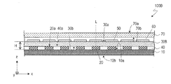
(第2の実施形態)
図7は、本開示の第2の実施形態による発光装置の断面を模式的に示す。図7に示す発光装置100Bは、図1等を参照して説明した発光装置100Aの波長変換層30Aに代えて、複数の光源20の側面を覆う保護層40と、保護層40上の波長変換層30Bとを有する。以下、保護層40および波長変換層30Bの詳細を説明する。
(Second embodiment)
FIG. 7 schematically shows a cross section of a light emitting device according to the second embodiment of the present disclosure. The light emitting device 100B shown in FIG. 7 has a protective layer 40 covering the side surfaces of a plurality of light sources 20 and wavelength conversion on the protective layer 40, instead of the wavelength conversion layer 30A of the light emitting device 100A described with reference to FIG. It has a layer 30B. Hereinafter, the details of the protective layer 40 and the wavelength conversion layer 30B will be described.
[保護層40]
保護層40は、光源20の少なくとも側面を覆う層であり、ここでは、透明樹脂層である。ここでは、保護層40の上面40aは、光源20の上面20a(例えば発光素子22の上面22a、あるいは光反射層24の表面24a)に整合している。保護層40は、光源20の配置された基板10上に、エポキシ樹脂、シリコーン樹脂またはこれらを混合した樹脂を付与し、硬化させることによって形成することができる。透光性の樹脂材料の硬化後に、樹脂材料の硬化によって得られた樹脂層を基板10とは反対側から研削することにより、上面40aにおいて光源20の上面20aが露出された保護層40を形成することができる。
[Protective layer 40]
The protective layer 40 is a layer that covers at least the side surface of the light source 20, and is a transparent resin layer here. Here, the upper surface 40a of the protective layer 40 is aligned with the upper surface 20a of the light source 20 (for example, the upper surface 22a of the light emitting element 22 or the surface 24a of the light reflecting layer 24). The protective layer 40 can be formed by applying an epoxy resin, a silicone resin, or a resin in which these are mixed to the substrate 10 on which the light source 20 is arranged and curing the resin. After the translucent resin material is cured, the resin layer obtained by curing the resin material is ground from the side opposite to the substrate 10 to form a protective layer 40 on the upper surface 40a where the upper surface 20a of the light source 20 is exposed. can do.
[波長変換層30B]
図7に例示する構成において、波長変換層30Bは、シート形状(または層形状)を有し、保護層40上に位置する。図7に示すように、波長変換層30Bは、その下面30bが光源20の上面20aに接するようにして保護層40上に配置される。
[Wavelength conversion layer 30B]
In the configuration exemplified in FIG. 7, the wavelength conversion layer 30B has a sheet shape (or layer shape) and is located on the protective layer 40. As shown in FIG. 7, the wavelength conversion layer 30B is arranged on the protective layer 40 so that the lower surface 30b thereof is in contact with the upper surface 20a of the light source 20.
上述したように、本開示の実施形態によれば、光源20を狭ピッチで配列することが可能であり、したがって各光源20に投入する電力を低減しながら十分な輝度を確保し得る。光源20に投入する電力を低減することによって光源20から発せられる熱を低減でき、熱に起因する波長変換部材の劣化が抑制される。したがって、図7に示すような、波長変換層30Bが光源20の上面20aに接する構成を採用することが可能である。
As described above, according to the embodiments of the present disclosure, the light sources 20 can be arranged at a narrow pitch, and therefore sufficient brightness can be ensured while reducing the power applied to each light source 20. By reducing the electric power applied to the light source 20, the heat generated from the light source 20 can be reduced, and the deterioration of the wavelength conversion member due to the heat can be suppressed. Therefore, as shown in FIG. 7, it is possible to adopt a configuration in which the wavelength conversion layer 30B is in contact with the upper surface 20a of the light source 20.
波長変換層30Bは、上述の波長変換層30Aと同様に、光源20から出射する光の少なくとも一部を吸収して光源20からの出射光の波長とは異なる波長の光を発する。波長変換層30Bは、上述の波長変換層30Aを形成するための材料を用いて形成することができる。例えば、波長変換層30Bを形成するための材料として、蛍光体等の波長変換部材が分散された樹脂材料を用いることができる。波長変換層30Bは、例えば、波長変換層30Bを形成するための材料を保護層40の上面40aおよび光源20の上面20aに付与することによって保護層40上に直接に形成することが可能である。あるいは、保護層40の形成された基板10とは別途に、蛍光体等の波長変換部材が分散された樹脂材料中の樹脂をBステージの状態とした蛍光体シートを準備し、そのシートを保護層40上に配置することによって波長変換層30Bを形成することも可能である。波長変換部材を含むシート(例えば蛍光体シート)を基板10とは別途に準備する場合、波長変換部材を分散させる材料として、樹脂に代えて、例えば、ガラス、アルミナ等を含有するセラミックスを用いることも可能である。
Similar to the wavelength conversion layer 30A described above, the wavelength conversion layer 30B absorbs at least a part of the light emitted from the light source 20 and emits light having a wavelength different from the wavelength of the light emitted from the light source 20. The wavelength conversion layer 30B can be formed by using the material for forming the wavelength conversion layer 30A described above. For example, as a material for forming the wavelength conversion layer 30B, a resin material in which a wavelength conversion member such as a phosphor is dispersed can be used. The wavelength conversion layer 30B can be formed directly on the protective layer 40, for example, by applying a material for forming the wavelength conversion layer 30B to the upper surface 40a of the protective layer 40 and the upper surface 20a of the light source 20. .. Alternatively, separately from the substrate 10 on which the protective layer 40 is formed, a phosphor sheet in which the resin in the resin material in which the wavelength conversion member such as a phosphor is dispersed is in the B stage state is prepared, and the sheet is protected. It is also possible to form the wavelength conversion layer 30B by arranging it on the layer 40. When a sheet containing a wavelength conversion member (for example, a fluorescent material sheet) is prepared separately from the substrate 10, ceramics containing, for example, glass, alumina, etc. should be used instead of the resin as a material for dispersing the wavelength conversion member. Is also possible.
第2の実施形態においても、波長変換層(ここでは波長変換層30B)の上面30a上に散乱反射部50が配置されている。波長変換層30B上に散乱反射部50を設けることにより、第1の実施形態と同様に、輝度むら低減の効果が得られる。図7に例示する構造は、例えば、波長変換部材を含むシートの一方の表面に、樹脂と、樹脂に分散した反射材の粒子とを含む材料から形成されたパターンおよび/または金属のパターンを例えば印刷法によって形成し、パターンが形成されたシートを保護層40上に配置することによって得られる。ただし、パターンが形成されたシートを保護層40上に配置した場合、光源20を覆う波長変換層30A上に直接に散乱反射部50を形成可能な第1の実施形態と比較して、基板10上の光源20と、波長変換層30B上の散乱反射部50との間にアラインメントずれが生じる可能性がある。しかしながら、第2の実施形態では、特許文献2に記載されているような、一方の主面上に反射層のパターンを有するシート状の蛍光体層をLEDチップの上面から離して配置する構成とは異なり、光源20の上面20aに近接して波長変換層30Bを配置できる。したがって、アラインメントずれの低減の点で従来の構成よりも有利といえる。なお、波長変換層30Bを形成するための材料を保護層40の上面40aおよび光源20の上面20aに付与することによって保護層40上に波長変換層30Bを形成し、その後、波長変換層30B上に散乱反射部50を形成すれば、第1の実
施形態と同様に、アラインメントずれの発生を抑制することが可能である。
Also in the second embodiment, the scattering reflection unit 50 is arranged on the upper surface 30a of the wavelength conversion layer (here, the wavelength conversion layer 30B). By providing the diffuse reflection unit 50 on the wavelength conversion layer 30B, the effect of reducing the luminance unevenness can be obtained as in the first embodiment. The structure exemplified in FIG. 7 has, for example, a pattern formed from a material containing a resin and particles of a reflective material dispersed in the resin on one surface of a sheet including a wavelength conversion member, and / or a metal pattern. It is obtained by arranging a sheet formed by a printing method and having a pattern formed on the protective layer 40. However, when the sheet on which the pattern is formed is arranged on the protective layer 40, the substrate 10 is compared with the first embodiment in which the scattering reflection unit 50 can be directly formed on the wavelength conversion layer 30A covering the light source 20. There is a possibility that an alignment shift will occur between the above light source 20 and the scattering reflection unit 50 on the wavelength conversion layer 30B. However, in the second embodiment, as described in Patent Document 2, a sheet-like phosphor layer having a pattern of a reflective layer on one main surface is arranged away from the upper surface of the LED chip. However, the wavelength conversion layer 30B can be arranged close to the upper surface 20a of the light source 20. Therefore, it can be said that it is more advantageous than the conventional configuration in terms of reducing the alignment deviation. The wavelength conversion layer 30B is formed on the protective layer 40 by applying the material for forming the wavelength conversion layer 30B to the upper surface 40a of the protective layer 40 and the upper surface 20a of the light source 20, and then on the wavelength conversion layer 30B. If the scattering reflection unit 50 is formed on the surface, it is possible to suppress the occurrence of alignment misalignment as in the first embodiment.
(変形例)
図8は、本開示の他の実施形態による発光装置の断面を模式的に示す。図8に示す発光装置100Cは、図7を参照して説明した発光装置100Bと比較して、基板10と波長変換層30Bとの間に位置する区分部材15をさらに有する。以下、区分部材15の詳細を説明する。
(Modification example)
FIG. 8 schematically shows a cross section of a light emitting device according to another embodiment of the present disclosure. The light emitting device 100C shown in FIG. 8 further has a dividing member 15 located between the substrate 10 and the wavelength conversion layer 30B as compared with the light emitting device 100B described with reference to FIG. 7. Hereinafter, the details of the division member 15 will be described.
[区分部材15]
区分部材15は、底部15bと、y方向に延びる壁部15ayとを有する。図8に示すように、壁部15ayは、x方向に隣接する2つの光源20の間に位置する。また、図8には現れていないが、区分部材15は、y方向に隣接する2つの光源20の間に、x方向に延びる壁部(壁部15ax、後述する図10参照)を有する。底部15bと、x方向において対向する2つの壁部15ayと、y方向において対向する2つの壁部15ax(図8において不図示)によって、開口17hを有する発光空間17が形成される。図8に例示する構成において、各光源20は、発光空間17内に位置している。光源20の上方には、発光空間17の開口17hを覆うように波長変換層30Bが配置される。
[Division member 15]
The dividing member 15 has a bottom portion 15b and a wall portion 15ay extending in the y direction. As shown in FIG. 8, the wall portion 15ay is located between two light sources 20 adjacent to each other in the x direction. Further, although not shown in FIG. 8, the dividing member 15 has a wall portion extending in the x direction (wall portion 15ax, see FIG. 10 described later) between two light sources 20 adjacent to each other in the y direction. A light emitting space 17 having an opening 17h is formed by a bottom portion 15b, two wall portions 15ay facing each other in the x direction, and two wall portions 15ax facing each other in the y direction (not shown in FIG. 8). In the configuration illustrated in FIG. 8, each light source 20 is located in the light emitting space 17. Above the light source 20, a wavelength conversion layer 30B is arranged so as to cover the opening 17h of the light emitting space 17.
図9は、図8に示す発光空間17のうちの1つとその周辺とを拡大して模式的に示す。y方向に延びる壁部15ayは、y方向に延びる一対の傾斜面15tを含む。図9に示すように、一対の傾斜面15tは、zx断面において発光空間17の開口17hに面している。壁部15ayは、頂部15cを有し、この例では、壁部15ayの頂部15cが波長変換層30Bの下面30bに接している。x方向に延びる壁部15ax(図8において不図示)も同様に、x方向に延びる一対の傾斜面15sを含み、一対の傾斜面15sも、yz断面(不図示)において、発光空間17の開口17hに面する。壁部15ax(不図示)も壁部15ayと同様に頂部15cを有し、この例では、壁部15axの頂部15cも波長変換層30Bの下面30bに接している。なお、壁部15ayの頂部15cまたは壁部15axの頂部15cが波長変換層に接することは必須ではない。ただし、壁部15ayおよび壁部15axの頂部15cが波長変換層に接していると、1つの発光空間17内の光源20から出射した光の、隣接する発光空間17への入射を抑制し得る。
FIG. 9 schematically shows one of the light emitting spaces 17 shown in FIG. 8 and its surroundings in an enlarged manner. The wall portion 15ay extending in the y direction includes a pair of inclined surfaces 15t extending in the y direction. As shown in FIG. 9, the pair of inclined surfaces 15t face the opening 17h of the light emitting space 17 in the zx cross section. The wall portion 15ay has a top portion 15c, and in this example, the top portion 15c of the wall portion 15ay is in contact with the lower surface 30b of the wavelength conversion layer 30B. Similarly, the wall portion 15ax extending in the x direction (not shown in FIG. 8) also includes a pair of inclined surfaces 15s extending in the x direction, and the pair of inclined surfaces 15s also have an opening of the light emitting space 17 in the yz cross section (not shown). Facing 17h. The wall portion 15ax (not shown) also has a top portion 15c like the wall portion 15ay, and in this example, the top portion 15c of the wall portion 15ax is also in contact with the lower surface 30b of the wavelength conversion layer 30B. It is not essential that the top 15c of the wall 15ay or the top 15c of the wall 15ax is in contact with the wavelength conversion layer. However, when the wall portion 15ay and the top portion 15c of the wall portion 15ax are in contact with the wavelength conversion layer, it is possible to suppress the incident of the light emitted from the light source 20 in one light emitting space 17 into the adjacent light emitting space 17.
区分部材15は、例えば、反射材を含有する樹脂等から形成され、光反射性を有する。区分部材15は、壁部15axの傾斜面15sおよび壁部15ayの傾斜面15tで、光源20から出射する光を発光空間17の開口17hに向けて反射させる。また、底部15bに入射する光も発光空間17の開口17h側へ反射させる。基板10上において複数の光源20のそれぞれを取り囲む区分部材15を設けることにより、光源20から出射される光を効率よく波長変換層(ここでは波長変換層30B)へ入射させることができ、光拡散板70の上面70a(例えば図8参照)における輝度を向上させ得る。
The classification member 15 is formed of, for example, a resin containing a reflective material and has light reflectivity. The dividing member 15 reflects the light emitted from the light source 20 toward the opening 17h of the light emitting space 17 on the inclined surface 15s of the wall portion 15ax and the inclined surface 15t of the wall portion 15ay. Further, the light incident on the bottom portion 15b is also reflected to the opening 17h side of the light emitting space 17. By providing the dividing member 15 surrounding each of the plurality of light sources 20 on the substrate 10, the light emitted from the light source 20 can be efficiently incident on the wavelength conversion layer (here, the wavelength conversion layer 30B), and the light is diffused. The brightness on the upper surface 70a of the plate 70 (see, for example, FIG. 8) can be improved.
図9に示すように、底部15bの中央には貫通孔15eが設けられ、貫通孔15e内に光源20が位置する。貫通孔15eの形状および大きさに特に制限はなく、光源20が内部に位置し得る形状および大きさであればよい。区分部材15の底部15bでの反射を利用する観点から、貫通孔15eの外縁が光源20の近傍に位置していると有益である。つまり、上面視において貫通孔15eと光源20との間に生じる間隙が狭いと光の利用効率を向上させ得るので有益である。
As shown in FIG. 9, a through hole 15e is provided in the center of the bottom portion 15b, and the light source 20 is located in the through hole 15e. The shape and size of the through hole 15e are not particularly limited, and may be any shape and size as long as the light source 20 can be located inside. From the viewpoint of utilizing the reflection at the bottom portion 15b of the dividing member 15, it is advantageous that the outer edge of the through hole 15e is located in the vicinity of the light source 20. That is, it is advantageous that the gap generated between the through hole 15e and the light source 20 is narrow in the top view because the light utilization efficiency can be improved.
上述したように、区分部材15は、光反射性を有する。例えば、酸化チタン、酸化アルミニウム、酸化ケイ素等の酸化物粒子からなる反射材を含有する樹脂を用いて区分部材15を形成してもよいし、反射材を含有しない樹脂を用いて成形した後、表面に反射材を設けてもよい。区分部材15の光源20からの出射光に対する反射率は、例えば、70%以
上である。
As described above, the partitioning member 15 has light reflectivity. For example, the classification member 15 may be formed by using a resin containing a reflective material composed of oxide particles such as titanium oxide, aluminum oxide, and silicon oxide, or after molding using a resin not containing a reflective material, the partitioning member 15 may be formed. A reflective material may be provided on the surface. The reflectance of the dividing member 15 with respect to the light emitted from the light source 20 is, for example, 70% or more.
区分部材15は、金型を用いた成形、または、光造形によって形成することができる。金型を用いた成形方法としては、射出成形、押出成形、圧縮成形、真空成形、圧空成形、プレス成形等の成形方法を適用することができる。例えば、PET等で形成された反射シートに真空成形と適用することによって、底部15bと、壁部15axおよび15ayとが一体的に形成された形状を得ることができる。反射シートの厚さは、例えば100~500μmである。
The dividing member 15 can be formed by molding using a mold or by stereolithography. As a molding method using a mold, a molding method such as injection molding, extrusion molding, compression molding, vacuum molding, pressure molding, press molding or the like can be applied. For example, by applying vacuum forming to a reflective sheet formed of PET or the like, a shape in which the bottom portion 15b and the wall portions 15ax and 15ay are integrally formed can be obtained. The thickness of the reflective sheet is, for example, 100 to 500 μm.
この例では、導体配線層12上に絶縁部材16が設けられており、区分部材15の底部15bの下面が、後述する絶縁部材16の上面16aに固定されている。なお、絶縁部材16と、壁部15ayの2つの傾斜面15t(あるいは壁部15axの2つの傾斜面15s)とに囲まれた部分は、中空であってもよいし、樹脂等によって埋められていてもよい。例えば、絶縁部材16と、壁部15ayの2つの傾斜面15tとに囲まれた部分が、区分部材15を形成するための材料で埋められていてもよい。
In this example, the insulating member 16 is provided on the conductor wiring layer 12, and the lower surface of the bottom portion 15b of the dividing member 15 is fixed to the upper surface 16a of the insulating member 16 described later. The portion surrounded by the insulating member 16 and the two inclined surfaces 15t of the wall portion 15ay (or the two inclined surfaces 15s of the wall portion 15ax) may be hollow or may be filled with resin or the like. You may. For example, a portion surrounded by the insulating member 16 and the two inclined surfaces 15t of the wall portion 15ay may be filled with a material for forming the dividing member 15.
図10は、区分部材15および光源20をz方向に沿って見たときの上面図である。図10では、3行3列に配列された9つの発光空間17が示されている。図示するように、各光源20は、x方向に延びる2つの壁部15axと、y方向に延びる2つの壁部15ayとによって囲まれている。この例では、光源20のx方向の配置ピッチPxおよびy方向の配置ピッチPyは、互いに等しい。したがって、ここでは、底部15bの外形は、正方形である。
FIG. 10 is a top view of the dividing member 15 and the light source 20 when viewed along the z direction. In FIG. 10, nine light emitting spaces 17 arranged in 3 rows and 3 columns are shown. As shown in the figure, each light source 20 is surrounded by two wall portions 15ax extending in the x direction and two wall portions 15ay extending in the y direction. In this example, the arrangement pitch Px in the x direction and the arrangement pitch Py in the y direction of the light source 20 are equal to each other. Therefore, here, the outer shape of the bottom portion 15b is a square.
上述したように、壁部15axは、x方向に延びる一対の傾斜面15sを含み、壁部15ayは、y方向に延びる一対の傾斜面15tを含む。一対の傾斜面15sのそれぞれは、x方向に延びる2つの辺の一方で互いに接続されており、頂部15cが構成されている。x方向に延びる2つの辺の他方は、底部15bに接続している。同様に、一対の傾斜面15tのそれぞれは、y方向に延びる2つの辺の一方で互いに接続されており、頂部15cが構成されている。y方向に延びる2つの辺の他方は、底部15bに接続している。底部15bは、2つの壁部15axおよび2つの壁部15ayによって囲まれた領域15rに位置する。
As described above, the wall portion 15ax includes a pair of inclined surfaces 15s extending in the x direction, and the wall portion 15ay includes a pair of inclined surfaces 15t extending in the y direction. Each of the pair of inclined surfaces 15s is connected to each other on one of the two sides extending in the x direction, forming a top portion 15c. The other of the two sides extending in the x direction is connected to the bottom 15b. Similarly, each of the pair of inclined surfaces 15t is connected to each other on one of the two sides extending in the y direction, forming a top portion 15c. The other of the two sides extending in the y direction is connected to the bottom 15b. The bottom portion 15b is located in a region 15r surrounded by two wall portions 15ax and two wall portions 15ay.
区分部材15によって区画される発光空間17は、複数の光源20をそれぞれ独立して駆動させた場合における、発光領域の最小単位である。したがって、複数の光源20を独立して駆動する場合、発光空間17は、面発光装置として発光装置100Cを光拡散板70の上面70a側から見たときの、ローカルディミングの最小単位となり、複数の光源20を独立して駆動すれば、最小単位でローカルディミング駆動が可能な発光装置が実現する。隣接する複数の光源20を同時に駆動し、ON/OFFのタイミングを同期させるように駆動すれば、より大きな単位でのローカルディミングによる駆動が可能となる。
The light emitting space 17 partitioned by the dividing member 15 is the minimum unit of the light emitting region when a plurality of light sources 20 are independently driven. Therefore, when a plurality of light sources 20 are independently driven, the light emitting space 17 becomes the minimum unit of local dimming when the light emitting device 100C is viewed from the upper surface 70a side of the light diffusing plate 70 as a surface light emitting device, and a plurality of light sources 20 are driven independently. If the light source 20 is driven independently, a light emitting device capable of local dimming drive in the smallest unit is realized. If a plurality of adjacent light sources 20 are simultaneously driven and driven so as to synchronize the ON / OFF timings, it is possible to drive by local dimming in a larger unit.
[絶縁部材16]
上述したように、この例では、区分部材15と導体配線層12との間に絶縁部材16が介在している。絶縁部材16には、貫通孔16eが設けられており、図10に示すように、各領域15rの光源20は、貫通孔16e内に位置する。
[Insulation member 16]
As described above, in this example, the insulating member 16 is interposed between the dividing member 15 and the conductor wiring layer 12. The insulating member 16 is provided with a through hole 16e, and as shown in FIG. 10, the light source 20 in each region 15r is located in the through hole 16e.
再び図9を参照する。絶縁部材16は、導体配線層12のうち、光源20および他の素子等に電気的に接続される領域以外の領域を覆う。絶縁部材16は、導体配線層12のうち、光源20および他の素子等が配置されない領域に絶縁性を付与するレジストとして機能する。
See FIG. 9 again. The insulating member 16 covers a region of the conductor wiring layer 12 other than the region electrically connected to the light source 20 and other elements. The insulating member 16 functions as a resist that imparts insulating properties to a region of the conductor wiring layer 12 in which the light source 20 and other elements are not arranged.
絶縁部材16は、例えば、エポキシ樹脂、ウレタン樹脂、アクリル樹脂、ポリカーボネート樹脂、ポリイミド樹脂、オキセタン樹脂、シリコーン樹脂、変成シリコーン樹脂等の樹脂材料を用いて形成することができる。酸化チタン、酸化アルミニウム、酸化ケイ素等の酸化物粒子からなる反射材を樹脂材料に分散させた材料から絶縁部材16を形成してもよい。このような材料を用いて、光反射性を有する絶縁部材16を導体配線層12上に設けることにより、光源20からの光を基板10の上面10a側において反射させ、基板10側での光の漏れおよび吸収を防いで、発光装置100Cの光取り出し効率を向上させることが可能である。光源20からの出射光に対する絶縁部材16の反射率は、例えば、70%以上である。
The insulating member 16 can be formed by using a resin material such as an epoxy resin, a urethane resin, an acrylic resin, a polycarbonate resin, a polyimide resin, an oxetane resin, a silicone resin, or a modified silicone resin. The insulating member 16 may be formed from a material in which a reflective material composed of oxide particles such as titanium oxide, aluminum oxide, and silicon oxide is dispersed in a resin material. By using such a material and providing an insulating member 16 having light reflectivity on the conductor wiring layer 12, the light from the light source 20 is reflected on the upper surface 10a side of the substrate 10, and the light on the substrate 10 side is reflected. It is possible to prevent leakage and absorption and improve the light extraction efficiency of the light emitting device 100C. The reflectance of the insulating member 16 with respect to the light emitted from the light source 20 is, for example, 70% or more.
光反射性を有する絶縁部材16に入射した光を光源20の上方に向けて反射させて光の利用効率を高める観点からは、上面視において、貫通孔16eの外縁と光源20との間に生じる間隙が狭い方が有利である。ただし、貫通孔16eの外縁と光源20との間に生じる間隙を小さくすると、光源20の直上に向けて反射される光の割合が増加し、輝度むらが発生しやすくなる。本開示の実施形態では、波長変換層(ここでは波長変換層30B)上に、光源20の上面の少なくとも一部の上方に位置する散乱反射部50が設けられている。したがって、光源20の直上およびその付近の光を散乱反射部50によって散乱反射させることができ、貫通孔16eと光源20との間に生じる間隙を小さくした場合であっても、光源20の直上における輝度を低減して輝度むらを抑制することが可能である。
From the viewpoint of increasing the light utilization efficiency by reflecting the light incident on the light-reflecting insulating member 16 toward the upper side of the light source 20, it occurs between the outer edge of the through hole 16e and the light source 20 in the top view. It is advantageous that the gap is narrow. However, if the gap generated between the outer edge of the through hole 16e and the light source 20 is made small, the proportion of light reflected directly above the light source 20 increases, and uneven brightness is likely to occur. In the embodiment of the present disclosure, a scattering reflection unit 50 located above at least a part of the upper surface of the light source 20 is provided on the wavelength conversion layer (here, the wavelength conversion layer 30B). Therefore, the light directly above and in the vicinity of the light source 20 can be scattered and reflected by the scattering reflection unit 50, and even when the gap generated between the through hole 16e and the light source 20 is reduced, the light directly above the light source 20 It is possible to reduce the brightness and suppress the uneven brightness.
絶縁部材16の上面16aには、例えば接着部材によって区分部材15が固定される。接着部材は、両面テープであってもよいし、ホットメルト型の接着シートであってもよいし、熱硬化樹脂または熱可塑樹脂の接着液であってもよい。接着部材が高い難燃性を有すると有益である。貫通孔15eの周囲に接着部材を配置することにより、絶縁部材16と区分部材15との間に光源20からの出射光が入射することを抑制し得る。例えば、貫通孔15eの外縁に沿ってリング状に接着部材を配置してもよい。区分部材15の固定は、接着部材による固定に限定されず、ネジ、ピン等他の結合部材によって区分部材15を絶縁部材16に固定してもよい。
The dividing member 15 is fixed to the upper surface 16a of the insulating member 16 by, for example, an adhesive member. The adhesive member may be a double-sided tape, a hot-melt type adhesive sheet, or a thermosetting resin or a thermoplastic resin adhesive liquid. It is beneficial if the adhesive member has high flame retardancy. By arranging the adhesive member around the through hole 15e, it is possible to suppress the incident light emitted from the light source 20 between the insulating member 16 and the dividing member 15. For example, the adhesive member may be arranged in a ring shape along the outer edge of the through hole 15e. The fixing of the dividing member 15 is not limited to the fixing by the adhesive member, and the dividing member 15 may be fixed to the insulating member 16 by other connecting members such as screws and pins.
なお、この例では、壁部15ayおよび15axで規定される発光空間17に保護層40の材料が充填されている。絶縁部材16の上面16aに区分部材15を固定し、区分部材15側から保護層40の材料を付与して保護層40の材料を硬化させた後、硬化後の材料を壁部15ayおよび15axの頂部15cの位置まで研削することにより、光源20の側面を覆う保護層40を形成することができる。その後、保護層40上に波長変換層30Bおよび散乱反射部50を順次に形成するか、あるいは、一方の主面上に散乱反射部50が設けられた、波長変換部材が分散されたシートを保護層40上に配置することにより、図9に示すような構造が得られる。
In this example, the light emitting space 17 defined by the wall portions 15ay and 15ax is filled with the material of the protective layer 40. The partitioning member 15 is fixed to the upper surface 16a of the insulating member 16, the material of the protective layer 40 is applied from the partitioning member 15 side to cure the material of the protective layer 40, and then the cured material is applied to the wall portions 15ay and 15ax. By grinding to the position of the top 15c, the protective layer 40 covering the side surface of the light source 20 can be formed. After that, the wavelength conversion layer 30B and the scattering reflection unit 50 are sequentially formed on the protective layer 40, or the scattering reflection unit 50 is provided on one of the main surfaces to protect the sheet in which the wavelength conversion member is dispersed. By arranging it on the layer 40, the structure as shown in FIG. 9 can be obtained.
あるいは、発光空間17を、樹脂に波長変換部材が分散された材料で充填してもよい。図11に示す発光装置100Dは、上面30aに散乱反射部50が配置された波長変換層30Dが複数の光源20を覆う点で、図1を参照して説明した発光装置100Aと共通する。ただし、発光装置100Dは、区分部材15を有し、波長変換層30Dが区分部材15を覆っている。このような構成によっても、光拡散板70の上面70aにおける輝度を向上させ得る。基板10の上面10aから頂部15cまでの距離(頂部15cの高さ)は、基板10の上面10aから散乱反射部50までの距離H等に応じて適宜調整すればよい。頂部15cが波長変換層30Dから露出していてもよい。
Alternatively, the light emitting space 17 may be filled with a material in which a wavelength conversion member is dispersed in a resin. The light emitting device 100D shown in FIG. 11 is common to the light emitting device 100A described with reference to FIG. 1 in that the wavelength conversion layer 30D in which the scattering reflection unit 50 is arranged on the upper surface 30a covers the plurality of light sources 20. However, the light emitting device 100D has a division member 15, and the wavelength conversion layer 30D covers the division member 15. Even with such a configuration, the brightness on the upper surface 70a of the light diffusing plate 70 can be improved. The distance from the upper surface 10a of the substrate 10 to the top 15c (height of the top 15c) may be appropriately adjusted according to the distance H or the like from the upper surface 10a of the substrate 10 to the scattering reflection portion 50. The top 15c may be exposed from the wavelength conversion layer 30D.